technologies pcie gen 6
TRANSCRIPT

PCIe Gen 6Equalization Unraveled
Technologies
By -
P Shanmuga Srinivas
Technologies Page No #2PCIe Gen 6 Equalization Unraveled
Contents
Introduction. . . . . . . . . . . . . . . . . . . . . . . . . . . . . . . . . . . . . . . . . . . . . . . . . . . . . . . . . . . . . . . . . . . . . . . . . . . . 3
PCIe Gen6 Physical level changes. . . . . . . . . . . . . . . . . . . . . . . . . . . . . . . . . . . . . . . . . . . . . . . . 3
Implementation of Equalization in PCIe Gen 6. . . . . . . . . . . . . . . . . . . . . . . . . . . . . . 3
Equalization Procedure for PCIe Gen 6. . . . . . . . . . . . . . . . . . . . . . . . . . . . . . . . . . . . . . . . . 5
Additional Mechanisms for Equalization. . . . . . . . . . . . . . . . . . . . . . . . . . . . . . . . . . . . . . 9
Autonomous vs Software Based Equalization. . . . . . . . . . . . . . . . . . . . . . . . 9
Skipping Equalization in lower data rates. . . . . . . . . . . . . . . . . . . . . . . . . . . 9
Skipping Equalization. . . . . . . . . . . . . . . . . . . . . . . . . . . . . . . . . . . . . . . . . . . . . . . . . . . 9
Redo Equalization. . . . . . . . . . . . . . . . . . . . . . . . . . . . . . . . . . . . . . . . . . . . . . . . . . . . . . . 9
Ordered Sets. . . . . . . . . . . . . . . . . . . . . . . . . . . . . . . . . . . . . . . . . . . . . . . . . . . . . . . . . . . . . . . . . . . . . . . . . . . 10
EIOS: Electrical Idle Ordered Set. . . . . . . . . . . . . . . . . . . . . . . . . . . . . . . . . . . . . . . 10
EIEOS: Electrical Idle Exit Ordered Set. . . . . . . . . . . . . . . . . . . . . . . . . . . . . . . . 10
SKP: Skip Ordered Set. . . . . . . . . . . . . . . . . . . . . . . . . . . . . . . . . . . . . . . . . . . . . . . . . . . . 10
TS0: Training Sequence 0. . . . . . . . . . . . . . . . . . . . . . . . . . . . . . . . . . . . . . . . . . . . . . 10
TS1: Training Sequence 1. . . . . . . . . . . . . . . . . . . . . . . . . . . . . . . . . . . . . . . . . . . . . . . 12
About Us. . . . . . . . . . . . . . . . . . . . . . . . . . . . . . . . . . . . . . . . . . . . . . . . . . . . . . . . . . . . . . . . . . . . . . . . . . . . . . . . 13
LFT and PCIe. . . . . . . . . . . . . . . . . . . . . . . . . . . . . . . . . . . . . . . . . . . . . . . . . . . . . . . . . . . . . . . . . . . . . . . . . . 14
Technologies Page No #3PCIe Gen 6 Equalization Unraveled
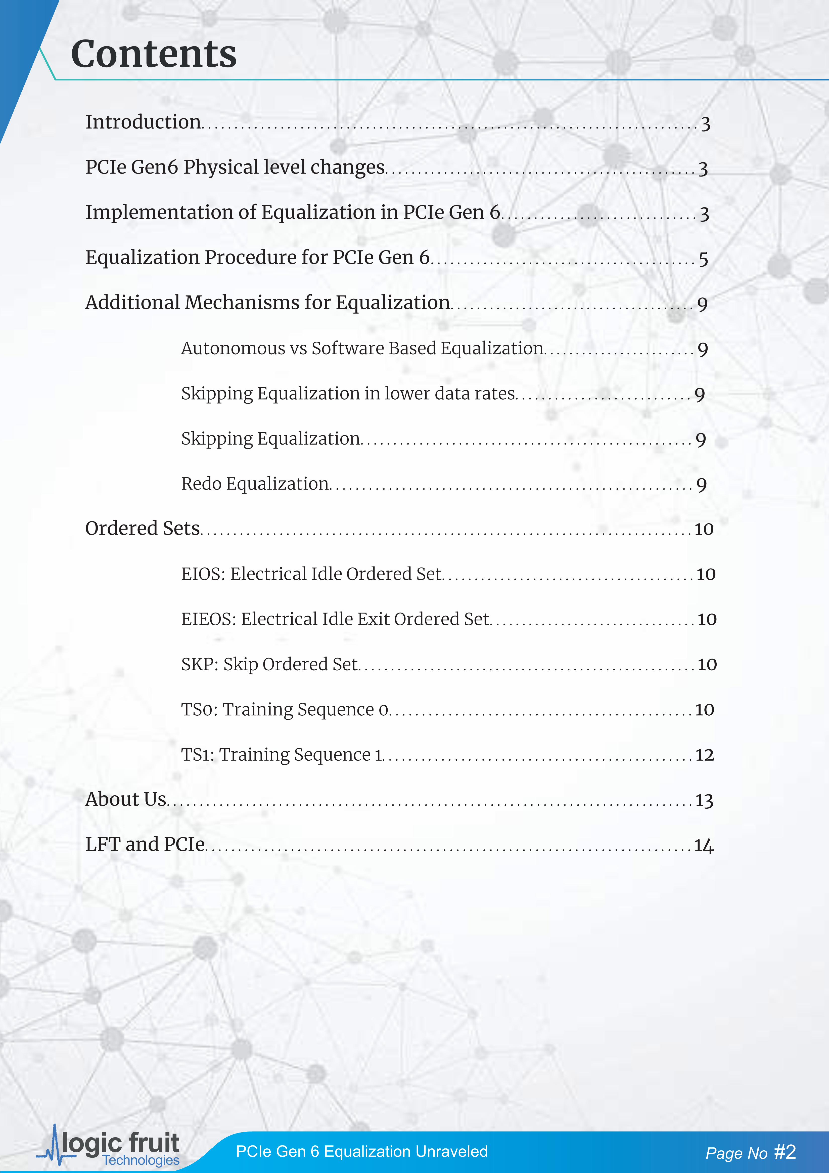
Introduction:Equalization is the process of compensating the distortion introduced by the channel. After passing
through a band-limited channel, the high frequency components of the signal are heavily attenuated
which distorts the signal and spreads it into subsequent symbol periods. This is visible as a closed eye in
the eye diagram. The process of equalization produces a sufficiently open eye as in Figure 1, and reduces
Inter Symbol Interference (ISI). This facilitates easier recovery of transmitted symbols, ultimately
reducing the Bit Error Rate (BER).
PCIe Gen6 Physical level changes:PAM4 is used in-place of NRZ in Gen 6 in order to achieve transfer speed of 64 GT/s, which significantly
increases the expected BER from 10-12 in previous generations to 10-6. To deal with the high BER,
Forward Error Correction (FEC) is used. Since, FEC works only on fixed-sized codes, gen 6 introduces Flit
(Flow Control Unit) which would be used for sending/receiving TLPs and DLLPs in a data stream. To keep
the latency low, a low-overhead FEC is used, and a strong flit level CRC for high reliability. Link level retry
is used at flit level, and ordered sets are replicated to further compensate for the high BER.
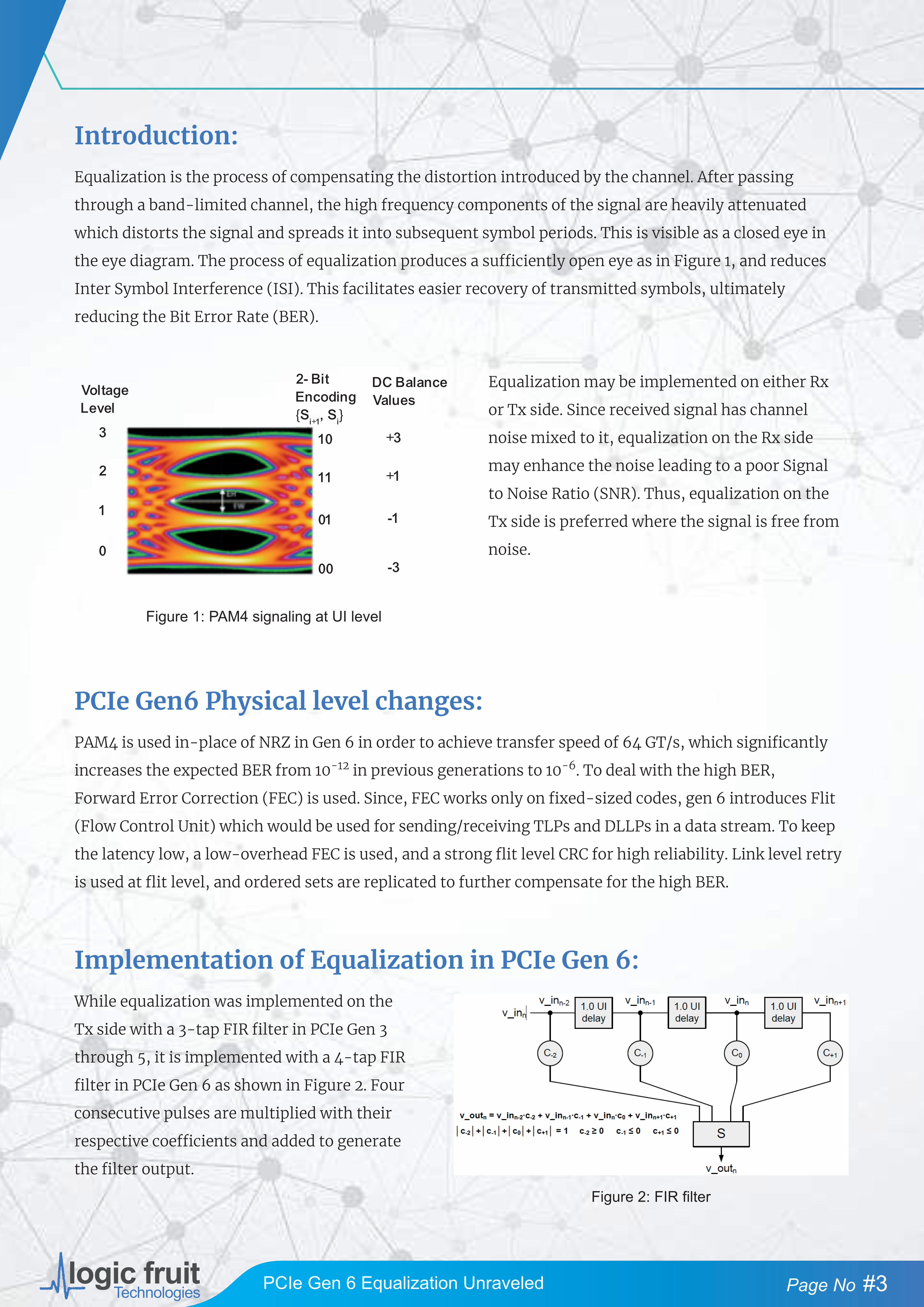
Implementation of Equalization in PCIe Gen 6:While equalization was implemented on the
Tx side with a 3-tap FIR filter in PCIe Gen 3
through 5, it is implemented with a 4-tap FIR
filter in PCIe Gen 6 as shown in Figure 2. Four
consecutive pulses are multiplied with their
respective coefficients and added to generate
the filter output.
Equalization may be implemented on either Rx
or Tx side. Since received signal has channel
noise mixed to it, equalization on the Rx side
may enhance the noise leading to a poor Signal
to Noise Ratio (SNR). Thus, equalization on the
Tx side is preferred where the signal is free from
noise.
Figure 1: PAM4 signaling at UI level
Figure 2: FIR filter
VoltageLevel
DC BalanceValues
2- BitEncoding{S
i+1, S
i}
3
2
1
0
10
11
01
00
+3
+1
-1
-3
Technologies Page No #4PCIe Gen 6 Equalization Unraveled
The coefficients C-2, C-1, C0, and C+1 are called 2nd precursor, precursor, cursor and postcursor.
The coefficients are required to satisfy the following rules:
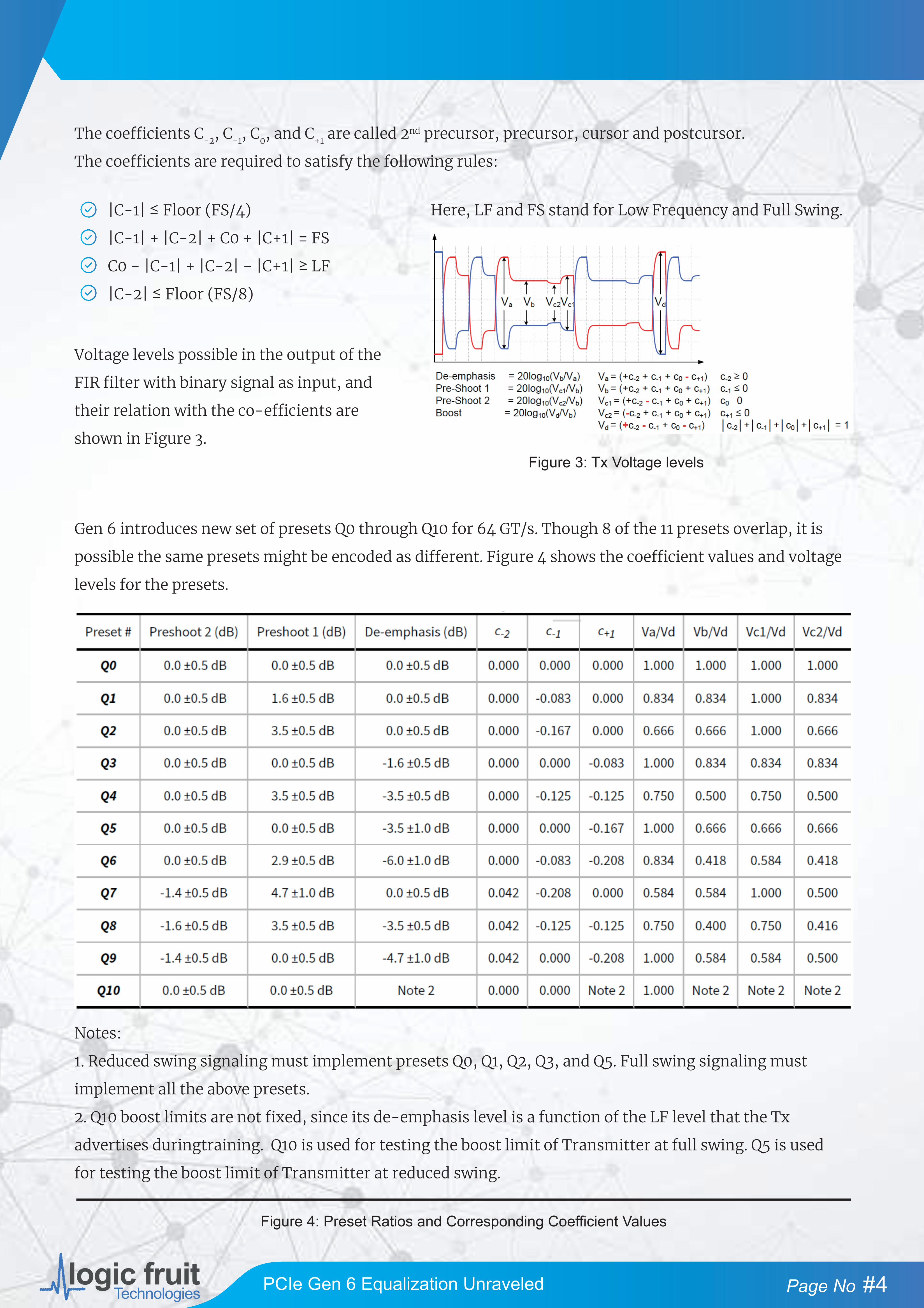
Voltage levels possible in the output of the
FIR filter with binary signal as input, and
their relation with the co-efficients are
shown in Figure 3.
Here, LF and FS stand for Low Frequency and Full Swing.
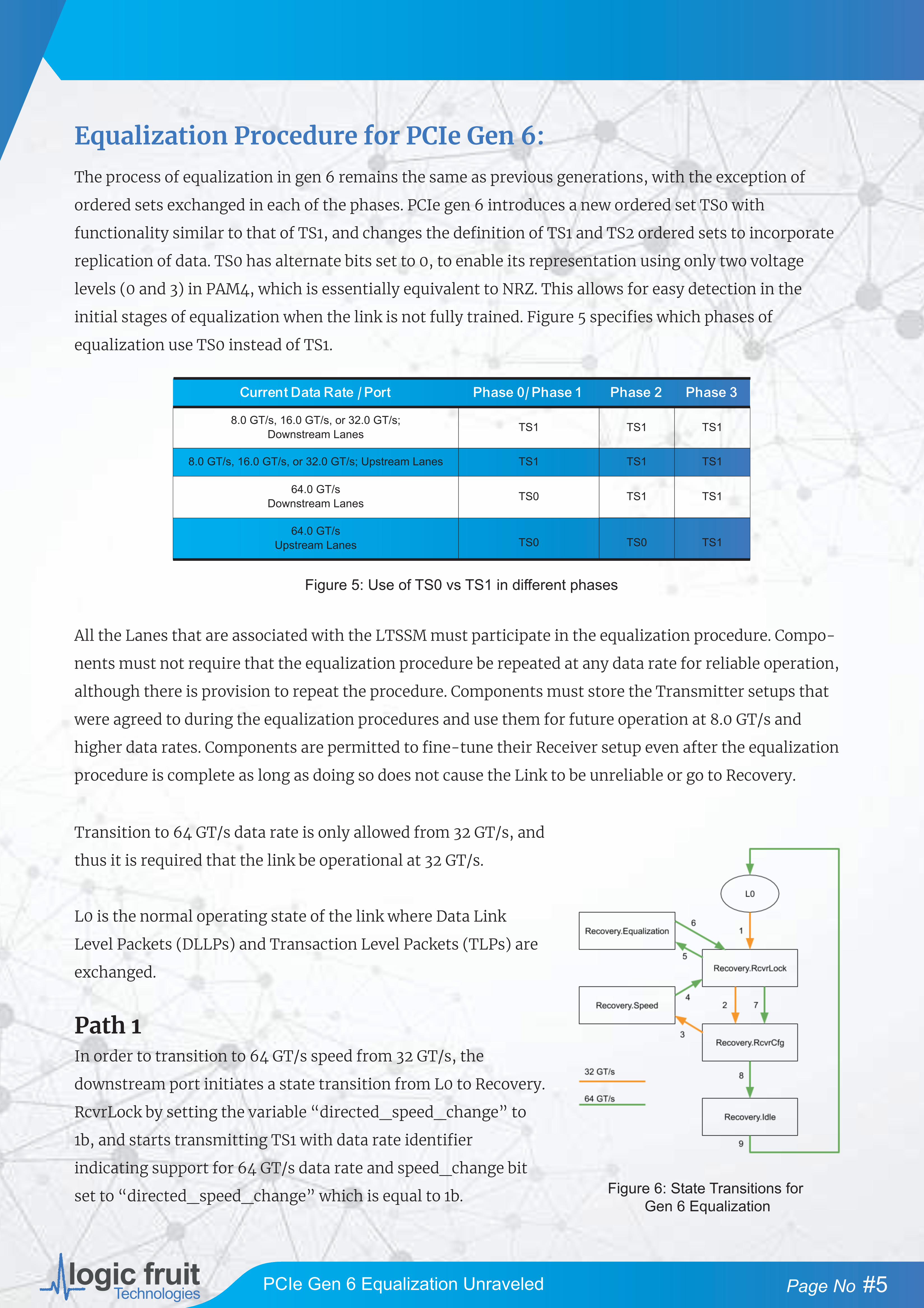
Gen 6 introduces new set of presets Q0 through Q10 for 64 GT/s. Though 8 of the 11 presets overlap, it is
possible the same presets might be encoded as different. Figure 4 shows the coefficient values and voltage
levels for the presets.
Notes:
1. Reduced swing signaling must implement presets Q0, Q1, Q2, Q3, and Q5. Full swing signaling must
implement all the above presets.
2. Q10 boost limits are not fixed, since its de-emphasis level is a function of the LF level that the Tx
advertises duringtraining. Q10 is used for testing the boost limit of Transmitter at full swing. Q5 is used
for testing the boost limit of Transmitter at reduced swing.
Figure 3: Tx Voltage levels
Figure 4: Preset Ratios and Corresponding Coefficient Values
|C-1| ≤ Floor (FS/4)
|C-1| + |C-2| + C0 + |C+1| = FS
C0 − |C-1| + |C-2| − |C+1| ≥ LF
|C-2| ≤ Floor (FS/8)
Technologies Page No #5PCIe Gen 6 Equalization Unraveled
Equalization Procedure for PCIe Gen 6:The process of equalization in gen 6 remains the same as previous generations, with the exception of
ordered sets exchanged in each of the phases. PCIe gen 6 introduces a new ordered set TS0 with
functionality similar to that of TS1, and changes the definition of TS1 and TS2 ordered sets to incorporate
replication of data. TS0 has alternate bits set to 0, to enable its representation using only two voltage
levels (0 and 3) in PAM4, which is essentially equivalent to NRZ. This allows for easy detection in the
initial stages of equalization when the link is not fully trained. Figure 5 specifies which phases of
equalization use TS0 instead of TS1.
All the Lanes that are associated with the LTSSM must participate in the equalization procedure. Compo-
nents must not require that the equalization procedure be repeated at any data rate for reliable operation,
although there is provision to repeat the procedure. Components must store the Transmitter setups that
were agreed to during the equalization procedures and use them for future operation at 8.0 GT/s and
higher data rates. Components are permitted to fine-tune their Receiver setup even after the equalization
procedure is complete as long as doing so does not cause the Link to be unreliable or go to Recovery.
Transition to 64 GT/s data rate is only allowed from 32 GT/s, and
thus it is required that the link be operational at 32 GT/s.
L0 is the normal operating state of the link where Data Link
Level Packets (DLLPs) and Transaction Level Packets (TLPs) are
exchanged.
Path 1In order to transition to 64 GT/s speed from 32 GT/s, the
downstream port initiates a state transition from L0 to Recovery.
RcvrLock by setting the variable “directed_speed_change” to
1b, and starts transmitting TS1 with data rate identifier
indicating support for 64 GT/s data rate and speed_change bit
set to “directed_speed_change” which is equal to 1b.
Figure 5: Use of TS0 vs TS1 in different phases
Figure 6: State Transitions for Gen 6 Equalization
Current Data Rate / Port
8.0 GT/s, 16.0 GT/s, or 32.0 GT/s;Downstream Lanes
8.0 GT/s, 16.0 GT/s, or 32.0 GT/s; Upstream Lanes
64.0 GT/sDownstream Lanes
64.0 GT/sUpstream Lanes
Phase 0/ Phase 1 Phase 2 Phase 3
TS1
TS1
TS0
TS0 TS0
TS1 TS1
TS1 TS1
TS1 TS1
TS1
Technologies Page No #6PCIe Gen 6 Equalization Unraveled
The upstream port transitions from L0 to Recovery.RcvrLock after receiving these TS1 with
speed_change=1b, and also sets the variable “directed_speed_change” to 1b.
Path 2Both devices move to Recovery.RcvrCfg upon receiving 8 consecutive TS1 or TS2 with link and lane
numbers that match with what is being transmitted, the speed_change bit equal to the “directed_-
speed_change” variable and the EC field is 00b.
Transmitters send TS2 Ordered Sets on all configured Lanes using the same Link and Lane numbers that
were set after leaving Configuration and the speed_change bit (bit 7 of data rate identifier Symbol in TS2
Ordered Set) set to 1b since the directed_speed_change variable is already set to 1b.
The Downstream Port must transmit 128b/130b EQ TS2 Ordered Sets (TS2 Ordered Sets with Symbol 7 bit 7
set to 1b) on each configured Lane with the Transmitter Preset bits set to the values specified by the “64.0
GT/s Upstream Port Transmitter Preset bits” from the corresponding “64.0 GT/s Lane Equalization
Control Register Entry”.
The Upstream Port is permitted to transmit 128b/130b EQ TS2 Ordered Sets with the 64.0 GT/s Transmitter
Preset bits set to implementation specific values.
The Upstream Port sets the “start_equalization_w_preset” variable to 1b and updates the “Upstream
Port 64 GT/s Transmitter Preset field” of the “64 GT/s Lane Equalization Control Register Entry” with the
values received in the eight consecutive 128b/130b EQ TS2 Ordered Sets.
The Downstream Port sets the “start_equalization_w_preset” variable equal to 1b since the variable
“equalization_done_64GT_data_rate” is still 0b.
Path 3Both ports transition to Recovery.Speed after eight consecutive EQ TS2 or receiving 128b/130b EQ TS2
Ordered Sets on all configured Lanes with identical data rate identifiers, identical value in Symbol 6, and
the speed_change bit set to 1b. The Transmitter enters Electrical Idle after sending an EIOS and stays
there until the Receiver Lanes have entered Electrical Idle, and then additionally remains there for at least
800 ns on a successful speed negotiation (i.e., successful_speed_negotiation = 1b), following which
frequency of operation is changed to the new data rate of 64 GT/s.
Path 4The “directed_speed_change” variable will be reset to 0b, and changed_speed_recovery to 1b, following
which the components transition to Recovery.RcvrLock.
Technologies Page No #7PCIe Gen 6 Equalization Unraveled
The Upstream port uses the presets it registered in Recovery.RcvrCfg and the Downstream port uses the
presets set in “Downstream Port 64.0 GT/s Transmitter Preset field” of the “64.0 GT/s Lane Equalization
Control Register Entry”.
Path 5After attaining block alignment, both ports transition to Recovery.Equalization. The “equalization_-
done_64GT_data_rate” variable is set to 1b.
Phase 0: The Upstream Port sends TS0 with EC=00b, and preset values it received in Recovery.RcvrCfg and
the Pre-cursor Coefficient, Cursor Coefficient, and Post-cursor Coefficient fields set to values
corresponding to the Transmitter Preset bits. The Downstream Port skips Phase 0 and directly enters
Phase 1. Next phase for the Upstream port is Phase 1 if all the configured Lanes receive two consecutive
TS0/TS1 Ordered Sets with EC = 01b or if all the configured Lanes receive two consecutive TS0 Ordered Sets
with EC = 01b and Retimer Equalization Extend bit set to 0b.
Phase 1: The Downstream Port first enters Phase 1, and begins transmission of TS0 with EC=01b, and
preset field set to the preset value it is currently using. The Upstream Port, after adjusting its receiver
enough to progress with the equalization process, receives these TS0 ordered sets and transitions to Phase
1, where it also transmits TS0 with EC=01b, and preset field set to the current preset value. Both ports
exchange LF and FS values which would be necessary to generate coefficient requests satisfying the
coefficient rules in Phase 2 and 3. It is expected that the Link will operate at a BER of less than 10-4 before
the component is ready to move on to the next Phase.
Phase 2: The Downstream Port initiates transition to Phase 2 by transmitting TS1 with EC=10b. The
Upstream Port follows after receiving two consecutive TS1 with EC = 10b. In this phase the Upstream Port
helps the downstream port fine tune its transmitter setting along with its own receiver setting until a BER
of less than 10-6 is achieved. The Upstream port requests the Downstream port to either apply presets or
coefficients by indicating it in the use_preset field (Symbol 1,9: Bit 7) in TS0:
The Downstream port after receiving two consecutive TS0 ordered sets with the same request, chooses to
either accept or reject the requested settings. If it chooses to accept the requested settings, it applies them
on the transmitter and starts sending TS1 with the requested settings and the reject_coefficient bit (Sym-
bol 3,11 Bit 7) set to 0.
If use_preset = 1, the current request is for a preset change and the requested preset is set in the
appropriate field (Symbol 5,13).
If use_preset = 0, the current request is for a coefficient change and the requested coefficients are
set in the appropriate fields.
Technologies Page No #8PCIe Gen 6 Equalization Unraveled
If it chooses to reject the requested settings it starts sending TS1 with the requested settings and the
reject_coefficient bit (Symbol 3,11 Bit 7) set to 1. In case the requests are accepted, the Upstream port
evaluates the settings and requests new settings if required. This continues until the required BER is
achieved, after which the Upstream port makes the transition to Phase 3 after sending TS0 with EC=11b.
Phase 3: The Downstream Port also makes the transition to Phase 3 after receiving two consecutive TS1
with EC=11b. In this phase the Downstream Port helps the upstream port fine tune its transmitter setting
along with its own receiver setting until a BER of less than 10-6 is achieved after following a method
similar to Phase 2. The Downstream Port sends TS1 with EC=00b to indicate that it is satisfied with the
BER and thus the end of equalization procedure.
Path 6Following this, the Downstream Port sets Equalization 64.0 GT/s Phase 3 Successful and Equalization 64.0
GT/s Complete bits of the 64.0 GT/s Status Register to 1b, and transitions to Recovery.RcvrLock.
The Upstream Port enters Recovery.RcvrLock after receiving two consecutive TS1 with EC=00b, and sets
the Equalization 64.0 GT/s Phase 3 Successful and Equalization 64.0 GT/s Complete bits of the 64.0 GT/s
Status Register to 1b.
In Recovery.RcvrLock, both ports must set the Coefficient fields in the transmitted TS1 Ordered Sets to the
current Transmitter settings. The downstream port must additionally set its preset field if the last
accepted request in Phase 2 was a preset. The Upstream Port must evaluate the equalization coefficients or
preset received by all Lanes that receive eight TS1 Ordered Sets and note whether they are different from
the final set of coefficients or preset that was accepted in Phase 2 of the equalization process. Mismatches
are reported in Recovery.RcvrCfg by setting the Request Equalization bit of TS2 Ordered Sets.
Path 7Both devices move to Recovery.RcvrCfg upon receiving 8 consecutive TS1 or TS2 with link and lane
numbers that match with what is being transmitted, the speed_change bit is equal to the directed_-
speed_change variable and the EC field is 00b.
Path 8Transition to Recovery.Idle takes place for both devices either or both of the following conditions are true:
if eight consecutive TS2 Ordered Sets are received on all configured Lanes with the same Link and
Lane number that match what is being transmitted on those same Lanes, identical data rate
identifiers within each Lane, and the speed_change bit is 0b.
16 TS2 Ordered Sets are sent after receiving one TS2 Ordered Set without being interrupted by any
intervening EIEOS.

Technologies Page No #9PCIe Gen 6 Equalization Unraveled
The changed_speed_recovery variable is reset to 0b on entry to Recovery.Idle.
Path 9Transmitter sends one SDS Ordered Set sequence followed by a Control SKP Ordered Set on all configured
Lanes followed by IDLE Flits to start a Data Stream. The transition to L0 takes place upon receiving eight
consecutive IDLE Flits and sending 32 IDLE Flits after receiving one IDLE Flit.
Additional Mechanisms for Equalization:
Autonomous vs Software Based EqualizationThe equalization procedure can be initiated either autonomously or by software. It is strongly
recommended that components use the autonomous mechanism. However, a component that chooses not
to participate in the autonomous mechanism must have its associated software ensure that the software
based mechanism is applied prior to operating at that data rate.
Skipping Equalization in lower data ratesThere is providence to skip equalization for lower data rates and begin with equalization for 32 GT/s if
both components support data rates of 32 GT/s or higher, and the mechanism as advertised in TS1/TS2 or
modified TS1/TS2 ordered sets. After making the link operational in 32 GT/s (by performing equalization at
32 GT/s if necessary), the transition to 64 GT/s can be made. The link can be trained to be operational at 64
GT/s speed by performing 64 GT/s equalization.
Skipping EqualizationEqualization process can be entirely skipped and the link can operate in the highest data rate available if
all components support data rates of 32 GT/s or higher and “No Equalization Needed” mechanism. This
mechanism is advertised if the component is capable of retrieving settings from a prior equalization or it is
sure that it doesn’t require equalization in all data rates above 5.0 GT/s.
Redo EqualizationIf the Downstream Port detects equalization problems or the Upstream Port made an equalization redo
request, the Downstream Port may redo equalization prior to proceeding to operate at the data rate where
the equalization failed or performing equalization at a higher data rate. It is possible to attempt to redo
equalization at 64 GT/s only from the data rate of 32 GT/s.

Technologies Page No #10PCIe Gen 6 Equalization Unraveled
Ordered Sets:
The following are the new definitions of ordered sets in gen 6:
EIOS: Electrical Idle Ordered SetBefore a Transmitter enters Electrical Idle, it must always send an Electrical Idle Ordered Set unless
otherwise specified for 32.0 GT/s and 64.0 GT/s Data Rate.
For 128b/130b encoding, EIOS has all 16 symbols set to 66h, while for 1b/1b encoding it has even symbols
set to 0Ah and odd symbols set to A0h.
EIEOS: Electrical Idle Exit Ordered SetIt is a low frequency pattern transmitted periodically to help ensure that receiver Electrical Idle exit
circuitry can detect an exit from Electrical Idle. It is also periodically sent in between TS ordered sets.
SKP: Skip Ordered Set
SKP OS are used to compensate for the small differences in the frequencies of transmitter and receiver
clocks by having the receiver add or remove symbols from received SKP OS to keep the elastic buffer from
under-flowing and overflowing. When using Flit Mode, only Control SKP Ordered Sets are transmitted. A
transmitted SKP Ordered Set is 40 symbols (40B), and a received SKP Ordered Set can be 24, 32, 40, 48 or
56 symbols.
Symbol No.
0,2,4,...,22
1,3,5,...,23
24-27,28-31
32-40
A0h
0Ah
AAA000A0h
SKP symbol
SKP symbol
SKP_END
PHY Payload
Value Description

Technologies Page No #11PCIe Gen 6 Equalization Unraveled
Symbol
0,8 TS0 identifier
2,10 Bit 7,5,3,1 - Phase 0,1: FS[3:0] Phase 2: |C-1| [3:0]
6,14 Bit 3,1 - Phase 2: |C0| [5:4]Bit 5 - Retimer Equalization Extend
4,12 Bit 1 - Phase 0,1: LF[2] Phase 2: |C+1| [4]Bit 7,5,3 - Phase 0,1: LF[5:3] Phase 2: |C-2| [2:0]
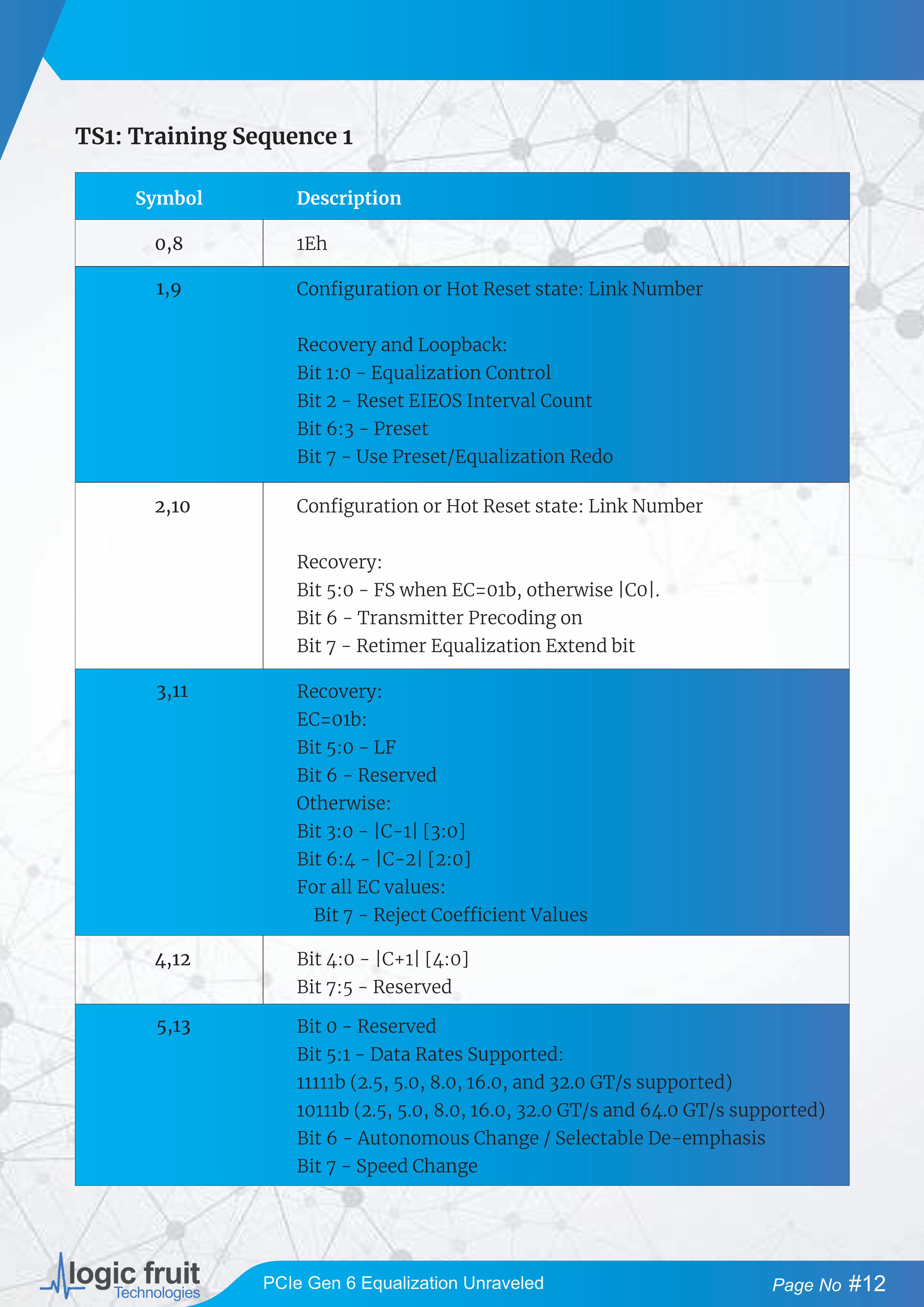
1,9 Bit 3,1 - Equalization Control (EC)Bit 5 - Reset EIEOS Interval CountBit 7 - Use Preset
7,15 If DC Balance adjustment is needed at start of TS0: 00h,02h,22h (Unscrambled)
Else:Bit 1,3,5,7 Half Scrambled Byte Level Even Parity
3,11 Bit 3,1 - Phase 0,1: FS[5:4] Phase 2: |C+1| [1:0]Bit 7,5 - Phase 0,1: LF[1:0] Phase 2: |C+1| [3:2]
5,13 Bit 7,5,3,1 - Phase 0,1: Preset [3:0]Phase 2: if Use Preset is 1b: Preset[3:0] Else: |C0| [3:0]
Description
TS0: Training Sequence 0
Even bits of all symbols are set to 0b for implementing NRZ
Technologies Page No #12PCIe Gen 6 Equalization Unraveled
Symbol
0,8 1Eh
2,10 Configuration or Hot Reset state: Link Number
Recovery:Bit 5:0 - FS when EC=01b, otherwise |C0|.Bit 6 - Transmitter Precoding onBit 7 - Retimer Equalization Extend bit
4,12 Bit 4:0 - |C+1| [4:0]Bit 7:5 - Reserved
1,9 Configuration or Hot Reset state: Link Number
Recovery and Loopback:Bit 1:0 - Equalization ControlBit 2 - Reset EIEOS Interval CountBit 6:3 - PresetBit 7 - Use Preset/Equalization Redo
3,11 Recovery:EC=01b:Bit 5:0 - LFBit 6 - ReservedOtherwise:Bit 3:0 - |C-1| [3:0]Bit 6:4 - |C-2| [2:0]For all EC values: Bit 7 - Reject Coefficient Values
5,13 Bit 0 - ReservedBit 5:1 - Data Rates Supported:11111b (2.5, 5.0, 8.0, 16.0, and 32.0 GT/s supported)10111b (2.5, 5.0, 8.0, 16.0, 32.0 GT/s and 64.0 GT/s supported)Bit 6 - Autonomous Change / Selectable De-emphasisBit 7 - Speed Change
Description
TS1: Training Sequence 1

Technologies Page No #13PCIe Gen 6 Equalization Unraveled
6,14 Bit 3:0 - 0000b : Deassert0001b : Assert Hot Reset0010b : Assert Disable0100b : Assert Loopback - the Follower Port at Receiver (A or F) loops back to its Transmitter.0101b : Assert Loopback – the Pseudo-Port Receiver B or C loops back to its Transmitter.0110b : Assert Loopback – the Pseudo-Port Receiver D or E loops back to its Transmitter.1000b : Assert Compliance Receive BitOthers : Reserved
Bit 7:4 Reserved
7,15 If DC Balance needs adjustment at the start of the TS1:DC Balance Symbol
else:Symbol 7 = Symbol 0 ^ Symbol 1 ^ … Symbol 6Symbol 15 = Symbol 8 ^ Symbol 9 ^ … Symbol 14

Technologies Page No #14PCIe Gen 6 Equalization Unraveled
LFT and PCIe:
We have worked on RTL IP and sub-system design for Latest generation of PCIe and other high speed
serial protocols, and development of device drives. Verification is done using the latest methodologies like
UVM and RTL-SW co-simulation. We also perform FPGA prototyping, validation, and testing with real
DUTs. Development of reference hardware is done with different kind of PCIe devices and links.
About Us
At Logic Fruit, we specialize in Architecting, Implementing and Validation high-quality real-time high
throughput FPGA/SoC embedded solutions, and Developing Proof-of-concept (PoC) designs/prototypes
real-time data generation, acquisition and analysis.
Our engineers have expertise with many high speed protocols and interfaces, including 1G, /10G/40G/100G
Ethernet, PCIe(Gen1-Gen6), USB3.0/4.0, CPRI/ORAN, DisplayPort, ARINC818 etc.
The team also has deep expertise in Signal processing for wireless and Imaging based solution
development, software-defined radio (SDR), as well as encryption, protocol compliance, signal
generation, data analysis, IoT technology, and multiple image processing techniques.

Thank You!Does anyone have any questions?
Technologies
By -
P Shanmuga Srinivas
Contact Us
806, 8th Floor BPTP Park CentraSector–30, NH–8 Gurgaon – 122001
Haryana (India)
+91 124-4285383