an1104: making accurate pcie gen 4.0 and gen 5.0 clock
TRANSCRIPT

AN1104: Making Accurate PCIe Gen 4.0and Gen 5.0 Clock Jitter Measurements
The Silicon Labs' Si5332 clock generator and Si522xx family ofclock generators and Si532xx buffers are designed to meet all therequirements detailed in PCIe Gen 4.0 and Gen 5.0 standards.It is typical for standards to become more demanding as data rates increase. PCI-Ex-press standards are no different, going from PCIe Gen 3.1 where the jitter requirementis 1.0ps RMS to PCIe Gen 4.0 where the jitter requirement is 0.5ps RMS, to only 0.15psin the current PCIe Gen 5.0 standard. This application note will discuss the issues whenmeasuring PCIe Gen 4.0 and Gen 5.0 in time domain and the best practices to resolvethem. By following the recommended methodology, results will provide accurate timedomain results. The principles in this application note can be applied to time domain jit-ter measurements for most clock based timing solutions including PCIe Gen1/2/3 meas-urements.
KEY POINTS
• Silicon Labs PCIe Clock Jitter Tool is aneasy-to-use software for PCIe jittermeasurements
• Even the best oscilloscopes contributenoise when making time based jittermeasurements.
• Corrections to time domain jittermeasurements can made using phasenoise based measurements.
silabs.com | Building a more connected world. Rev. 0.2

1. Introduction
PCIe Gen 4.0 and Gen 5.0 jitter requirement are challenging compared to earlier PCIe releases. This demanding jitter requirement re-quires an improvement in PCIe clock source performance and a reduction in the test equipment jitter contribution. Improving test equip-ment may not be possible, in which case the oscilloscope's jitter must be mathematically accounted for, resulting in a corrected andaccurate Device Under Test (DUT) measurement value. At the time of this writing, even the best oscilloscope will add excessive jitter tothe measured results. Therefore, the focus of this application note is to describe the process of quantifying and subtracting the oscillo-scope's jitter contribution to the overall measurement result.
The oscilloscope will introduce noise errors due to the input amplifier noise as well as the A/D clock quantization noise, as shown inFigure 1.1 Illustration of how the oscilloscope amplitude noise degrades the jitter measurements. on page 2. We must keep in mindthat the oscilloscope amplitude noise to jitter relationship is affected by the reference clock slew rate which requires the oscilloscopenoise to be characterized under each input slew rate, such as when analyzing DUTs having different performance. Additionally, oscillo-scope settings must be fully optimized. Finally, hardware must be fully optimized as well, including Printed Circuit Board, layout, termi-nation methodology, cable length matching, and power supply noise filtering.
The recommended best method is to first measure the DUT with a Phase Noise Analyzer, PNA. We used a Keysight E5052 in ourexample. Because the PNA will not lock to a signal with large modulation, the DUT spread spectrum feature must be turned off. TheDUT time domain jitter is then measured with a high speed/low noise Digital Storage Oscilloscope (DSO). We used a KeysightDSA90804 in our example, again with the spread spectrum turned off. Root Sum Square analysis can then be applied to the results ofthese two measurements in order to estimate the oscilloscope's jitter contribution.
Figure 1.1. Illustration of how the oscilloscope amplitude noise degrades the jitter measurements.
AN1104: Making Accurate PCIe Gen 4.0 and Gen 5.0 Clock Jitter MeasurementsIntroduction
silabs.com | Building a more connected world. Rev. 0.2 | 2

2. PCIe Clock Timing Schemes, Jitter Measurement and Correction Methodology
PCIe Gen 4.0 and Gen 5.0 have two different clock architectures, either shared clock or independent clock. The first is referred to asCommon Clock Architecture where the transmit and receive sides share the same clock. See Figure 2.1 Common Clock Architecture onpage 3. The second clock architecture involves two independent clocks which are referred to as Separate RefClk with no SpreadSpectrum (SRNS) or Separate RefClk with Independent Spread Spectrum Clock (SRIS), in which there are separate reference clockson the transmit side and on the receive side. See Figure 2.2 SRNS/SRIS Clock Architecture on page 3.
Figure 2.1. Common Clock Architecture Figure 2.2. SRNS/SRIS Clock Architecture
The clock and data retiming section, CDR, includes a low pass filter function in both timing architectures. The CDR filter will track lowfrequencies and provide correct clock and data alignment. The key difference between the two is the noise in the Common Clock Archi-tecture is a function of the transmit and receive PLL BW differences. Whereas in the SRNS/SRIS scheme the reference clocks areindependent of each other and given their dominant jitter is random, their combined impact on the system is the root sum square of theindividual terms, resulting in higher overall jitter - potentially requiring lower clock noise solutions. SRNS/SRIS will also need to correctfor the differences in clock accuracy between the transmit and receive sides, which can potentially degrade latency performance. SRNSand SRIS have the advantage of not relying on a shared clock which must be transmitted, simplifying the overall design.
It should be noted that there are many different filter combination schemes due to the various PCIe H1(s), H2(s) and H3(s) require-ments and definitions. Calculating these can be laborious. Silicon Labs' PCIe Clock Jitter Tool significantly simplifies this task by provid-ing either phase noise data or time domain data analysis capabilities. This application note can be used in conjunction with the PCIeClock Jitter Tool in order to accurately measure PCIe reference clock and/or buffer jitter.
The two methods to measure PCIe jitter, time domain and phase domain, have advantages and disadvantages. Therefore, combiningboth methods yields the most accurate results. A phase noise measurement is recognized as the most accurate tool to use when meas-uring low noise clocking sources such as crystal based oscillators, TCXO’s and OCXO’s. The disadvantage is that most phase-noiseanalyzers can only measure reference clocks with the spread spectrum turned off.
Time domain oscilloscopes have the advantage of measuring jitter with the spread spectrum turned off or on. The issue with a timedomain measurement is the relatively high noise floor of the instrument, on the order of -145 dBc compared to -180 dBc of a PNA. Thisperformance of the oscilloscope limits the jitter measurement accuracy when measuring Gen 4.0 or Gen 5.0 PCIe clocks.
In order to obtain the most accurate PCIe clock jitter measurement, we can/will combine both time and phase domain measurements.When both these measurements are collected, the data can be easily run through the PCIe Clock Jitter Tool and RSS subtraction isused to correct the DSO noise, resulting in accurate jitter measurements.
AN1104: Making Accurate PCIe Gen 4.0 and Gen 5.0 Clock Jitter MeasurementsPCIe Clock Timing Schemes, Jitter Measurement and Correction Methodology
silabs.com | Building a more connected world. Rev. 0.2 | 3

2.1 Phase Noise Measurement
Application specific phase noise test equipment has extremely low noise floor making them the choice for measuring low phase noisedevices such as crystal based oscillators. A Keysight E5052B is used in the examples presented. Phase noise is measured over arange of offsets, from 100 Hz to 40 MHz offset, for a 100.000 MHz PCIe reference clock Figure 2.4 shown below on page 5. In thisexample, the phase jitter was integrated from 12 kHz to 20 MHz, resulting in 242.895 fs rms. This data can be saved as a CSV file. Theunfiltered phased jitter over any integration band can be calculated using Silicon Labs Phase Noise to Jitter calculator (https://www.silabs.com/tools/pages/phase-noise-jitter-calculator.aspx). PCIe filtered phase jitter can be calculated using Silicon Labs PCIe Jit-ter Tool (https://www.silabs.com/products/timing/pci-express-learning-center). Since most PNAs do not provide data beyond 40 MHzoffset from the carrier, and the PCI-SIG determines integration range from 10 kHz to 50 MHz, the PCIe Clock Jitter Tool includes anoption to extend the noise floor of the CSV file to 50 MHz. As shown in Figure 2.3 PCIe Clock Jitter Tool Data File Input page on page4 below, the option to extend the noise floor is set by default. However, if the PNA is able to provide data until 50 MHz offset, thedata from PNA will not be affected even if this option is selected.
Figure 2.3. PCIe Clock Jitter Tool Data File Input Page with the extend phase noise data option enabled and the number ofnoise floor folds set to 3 by default.
Recent discussion in the PCIe community have questioned if second order effects such as the noise folding of frequencies beyond 50MHz are captured by the phase noise analyzers. In order to provide a conservative estimation of jitter, the PCIe Clock Jitter has thisoption available and enabled with 3 folds by default.
AN1104: Making Accurate PCIe Gen 4.0 and Gen 5.0 Clock Jitter MeasurementsPCIe Clock Timing Schemes, Jitter Measurement and Correction Methodology
silabs.com | Building a more connected world. Rev. 0.2 | 4

Figure 2.4. PCIe Clock Phase Noise Plot
Phase noise is measured at about 0.2 % increments of the offset range. The phase noise power is calculated for each of these discretefrequency bins, resulting in a bin value. The bin value contains only magnitude information, excluding phase. Time domain measure-ments, when processed through FFT, contain both magnitude and phase. See the Figure 2.5 figure below on page 5. It should benoted that integrating a phase noise based magnitude only, where all vectors are aligned (I A' - F' I), is always larger than an equivalenttime domain based magnitude plus phase measurement (I A – F I). Therefore, the phase noise based jitter measurement; a magnitudeonly measurement, is a conservative and legitimate method to use when measuring clock jitter.
I A’ -F’ I ≥ I A – F I
Phase Noise Analyzer Jitter, magnitude only
Time Domain FFT Jitter, magnitude and phase
Figure 2.5. Jitter Analysis
will automatically apply all appropriate PCIe filters on the phase noise data. The following sample files for Si52204 and Si5332 werecaptured using the E5052B and are available for reference. The two figures below show the compliance results.
https://www.silabs.com/documents/public/miscellaneous/si52204-pcie-sample-files.zip
https://www.silabs.com/documents/public/miscellaneous/si5332-sample-files.zip.
AN1104: Making Accurate PCIe Gen 4.0 and Gen 5.0 Clock Jitter MeasurementsPCIe Clock Timing Schemes, Jitter Measurement and Correction Methodology
silabs.com | Building a more connected world. Rev. 0.2 | 5
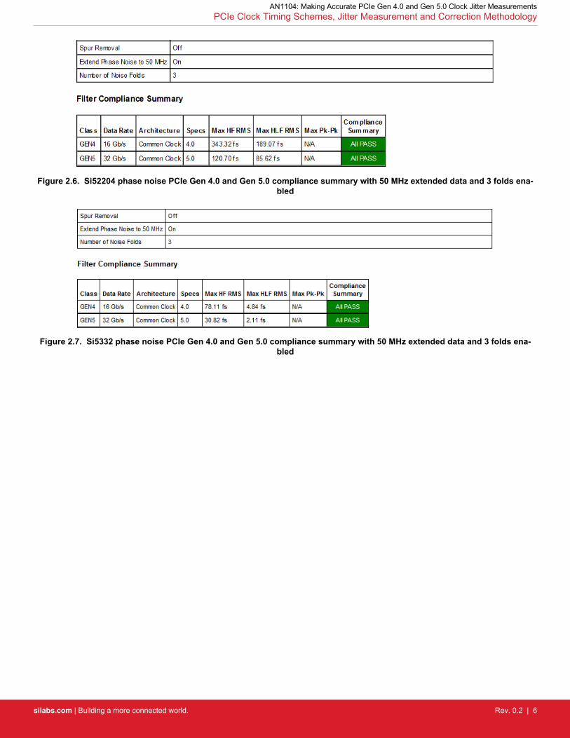
Figure 2.6. Si52204 phase noise PCIe Gen 4.0 and Gen 5.0 compliance summary with 50 MHz extended data and 3 folds ena-bled
Figure 2.7. Si5332 phase noise PCIe Gen 4.0 and Gen 5.0 compliance summary with 50 MHz extended data and 3 folds ena-bled
AN1104: Making Accurate PCIe Gen 4.0 and Gen 5.0 Clock Jitter MeasurementsPCIe Clock Timing Schemes, Jitter Measurement and Correction Methodology
silabs.com | Building a more connected world. Rev. 0.2 | 6

2.2 Oscilloscope Noise Measurement and Correction
Since most of the current PNA are not able to lock to reference clocks that have spread spectrum on, a DSO is required to measurejitter on these clocks. The oscilloscope noise, however, can be on the order of -142 dBc, well above the performance of Gen 4.0 andGen 5.0 clock generators and buffers. Phase jitter measurements as described in the previous section can be used to correct theDSO's noise by measuring the PCIe reference clock with the spread spectrum feature disabled. The equation below is used to calculatethe DSO's jitter noise.
J DSO,ADD = Square Root (J DSO,SSOFF2 – J PNA,SSOFF2)
Equation 2. Calculation of the added jitter noise from the DSO noise
The PCIe Clock Jitter with the spread turned on, is then corrected using the formula below, after measurements are made:
J DSO,CORRECTED = Square Root (J DSO,SSON2– J DSO,ADD2)
Equation 3. Correction formula to remove the contribution of the DSO jitter on time domain spread spectrum clocks meas-urements
But the accounting for the DSO is not only important to correct measurements with spread spectrum on. With the tighter jitter require-ments of PCIe Gen 4.0 and Gen 5.0 it is critical to account for the higher jitter floor of the DSO.
Figure 2.8 overlap of the phase noiase and oscilloscope data on page 7 shows the overlap of the phase jitter of the same part meas-ured with a E5052B PNA and two oscilloscopes: a DSA90804 and a MSO64. Both the scopes are set to operate with 8GHz bandwidthand 100mV/Div. The DSA90804 is sampling at 20GS/s and the MSO64 at 25GS/s.
Figure 2.8. Overlap of the measured phase jitter with the E5052B phase noise analyzer, and the oscilloscopes DSA90804 andMSO64
AN1104: Making Accurate PCIe Gen 4.0 and Gen 5.0 Clock Jitter MeasurementsPCIe Clock Timing Schemes, Jitter Measurement and Correction Methodology
silabs.com | Building a more connected world. Rev. 0.2 | 7

2.3 Jitter Correction Example
The following is an example of a Corrected PCIe Clock Jitter Measurement
The first step is to measure the phase noise of the DUT, with the spread spectrum turned off, and in this example the results are shownin Figure 2.4 PCIe Clock Phase Noise Plot on page 5. The phase noise results are also saved as a csv and imported when using PCIeClock Jitter Tool. Figure 2.9 Selecting the SSOFF phase noise data input and the PCIe filter on the Clock Jitter Tool on page 8shows the Unfiltered and PCIe Filtered jitter results for one of the H1(s) and H2(s) filter combinations versus offset frequency for thephase noise based measurement. This filter combination is known to give the worst case SSON jitter value based on the DSO results.
Figure 2.9. Selecting the SSOFF phase noise data input and the PCIe filter on the Clock Jitter Tool
Figure 2.10. Resulting jitter analysis of the phase noise measurement, spread off
The DUT is then measured with the spread off using a DSO, in this case with a Keysight DSA90804A. The PCIe Clock Jitter Tool isused to calculate the PCIe Filtered jitter with results shown in the figures below.
AN1104: Making Accurate PCIe Gen 4.0 and Gen 5.0 Clock Jitter MeasurementsPCIe Clock Timing Schemes, Jitter Measurement and Correction Methodology
silabs.com | Building a more connected world. Rev. 0.2 | 8

Figure 2.11. Selecting the SSOFF DSO data input and the PCIe filter on the Clock Jitter Tool
Figure 2.12. Resulting jitter analysis of the DSO measurement, spread off
The phase noise based measurement results in 24.4 fs rms when selecting the Gen 5.0 RSIS 1.8 MHz / 2 dB, 1.8 MHz / 2 dB filter.
The DSO based measurement results in 89.2 fs rms for the same filter.
The DSO scope noise is determined to be 85.8 fs rms, using the equation below.
DSO Jitter = Square Root (89.22– 24.42) = 85.8 fs
The DUT Spread Spectrum feature is enabled and a DSO measurement is made. The figure below shows the filtered and unfilteredphase noise verses frequency using the PCIe Clock Jitter Tool.
AN1104: Making Accurate PCIe Gen 4.0 and Gen 5.0 Clock Jitter MeasurementsPCIe Clock Timing Schemes, Jitter Measurement and Correction Methodology
silabs.com | Building a more connected world. Rev. 0.2 | 9

Figure 2.13. Selecting the SSON DSO data input and the PCIe filter on the Clock Jitter Tool
Figure 2.14. Resutling jitter analysis of the DSO measurement, spread on
The DUT PCIe reference clock with spread spectrum enabled based on the DSO measurement results in 112.45 fs rms worst case forthe Gen 5.0 RSIS 1.8 MHz / 2 dB, 1.8 MHz / 2 dB filter. Using the 85.8 fs correction factor for the same filter combination and theequation below results in 0.28 ps actual DUT performance.
Correct DUT Jitter = Square Root (112.452– 85.82) = 72.7 fs
This example shows uncorrected DUT performance of 112.4 fs versus a 72.7 fs corrected value. This difference can cause a false fail-ure, and it’s advised to use DSO noise correction when making Gen 5.0 and Gen 4.0 measurements. This same correction methodolo-gy can be applied to any DSO-based high-performance clock measurement.
AN1104: Making Accurate PCIe Gen 4.0 and Gen 5.0 Clock Jitter MeasurementsPCIe Clock Timing Schemes, Jitter Measurement and Correction Methodology
silabs.com | Building a more connected world. Rev. 0.2 | 10

3. Conclusions
The most accurate time domain jitter measurements will result when:1. Optimizing hardware set up.2. Optimizing test equipment settings.3. Measure phase noise with the spread spectrum turned off, add estimated readings out to 50 MHz offset as needed.4. Measure time domain jitter with the spread spectrum turned off with applicable DUT slew rate plus load.5. Measure time domain jitter with the spread spectrum turned on with applicable DUT slew rate plus load.6. Calculate test equipment contributed noise by RSS subtracting the results from steps 3 and 4.7. Calculate DUT performance by RSS subtracting the results from steps 5 and 6.
If you have questions about the information described in this document, please contact support at https://www.silabs.com/support.
To download Silicon Labs PCIe Clock Jitter Tool, visit this site: https://www.silabs.com/products/timing/pci-express-learning-center
AN1104: Making Accurate PCIe Gen 4.0 and Gen 5.0 Clock Jitter MeasurementsConclusions
silabs.com | Building a more connected world. Rev. 0.2 | 11

4. References
"Refclk Fanout Best Practices for 8GT/s and 16GT/s Systems," G. Richmond, Silicon Labs, presented at PCI-SIG Developers Confer-ence (June 7, 2017) in Santa Clara, CA.
“Removing Oscilloscope Noise from RMS Jitter Measurements” G Giust and F Benford, Jitter Labs (July 26, 2017)
AN1104: Making Accurate PCIe Gen 4.0 and Gen 5.0 Clock Jitter MeasurementsReferences
silabs.com | Building a more connected world. Rev. 0.2 | 12

IoT Portfoliowww.silabs.com/timing
SW/HWwww.silabs.com/CBPro
Qualitywww.silabs.com/quality
Support & Communitywww.silabs.com/community
ClockBuilder ProOne-click access to Timing tools, documentation, software, source code libraries & more. Available for Windows and iOS (CBGo only).
www.silabs.com/CBPro
Silicon Laboratories Inc.400 West Cesar ChavezAustin, TX 78701USA
www.silabs.com
DisclaimerSilicon Labs intends to provide customers with the latest, accurate, and in-depth documentation of all peripherals and modules available for system and software imple-menters using or intending to use the Silicon Labs products. Characterization data, available modules and peripherals, memory sizes and memory addresses refer to each specific device, and “Typical” parameters provided can and do vary in different applications. Application examples described herein are for illustrative purposes only. Silicon Labs reserves the right to make changes without further notice to the product information, specifications, and descriptions herein, and does not give warranties as to the accuracy or completeness of the included information. Without prior notification, Silicon Labs may update product firmware during the manufacturing process for security or reliability reasons. Such changes will not alter the specifications or the performance of the product. Silicon Labs shall have no liability for the consequences of use of the infor-mation supplied in this document. This document does not imply or expressly grant any license to design or fabricate any integrated circuits. The products are not designed or authorized to be used within any FDA Class III devices, applications for which FDA premarket approval is required or Life Support Systems without the specific written consent of Silicon Labs. A “Life Support System” is any product or system intended to support or sustain life and/or health, which, if it fails, can be reasonably expected to result in significant personal injury or death. Silicon Labs products are not designed or authorized for military applications. Silicon Labs products shall under no circumstances be used in weapons of mass destruction including (but not limited to) nuclear, biological or chemical weapons, or missiles capable of delivering such weapons. Silicon Labs disclaims all express and implied warranties and shall not be responsible or liable for any injuries or damages related to use of a Silicon Labs product in such unauthorized applications. Note: This content may contain offensive terminology that is now obsolete. Silicon Labs is replacing these terms with inclusive language wherever possible. For more information, visit www.silabs.com/about-us/inclusive-lexicon-project
Trademark InformationSilicon Laboratories Inc.®, Silicon Laboratories®, Silicon Labs®, SiLabs® and the Silicon Labs logo®, Bluegiga®, Bluegiga Logo®, Clockbuilder®, CMEMS®, DSPLL®, EFM®, EFM32®, EFR, Ember®, Energy Micro, Energy Micro logo and combinations thereof, “the world’s most energy friendly microcontrollers”, Ember®, EZLink®, EZRadio®, EZRadioPRO®, Gecko®, Gecko OS, Gecko OS Studio, ISOmodem®, Precision32®, ProSLIC®, Simplicity Studio®, SiPHY®, Telegesis, the Telegesis Logo®, USBXpress® , Zentri, the Zentri logo and Zentri DMS, Z-Wave®, and others are trademarks or registered trademarks of Silicon Labs. ARM, CORTEX, Cortex-M3 and THUMB are trademarks or registered trademarks of ARM Hold-ings. Keil is a registered trademark of ARM Limited. Wi-Fi is a registered trademark of the Wi-Fi Alliance. All other products or brand names mentioned herein are trademarks of their respective holders.