eight output differential buffer for pcie gen 2...
TRANSCRIPT
ICS9DB803DI
IDTTM/ICSTM Eight Output Differential Buffer for PCIe Gen 2 ICS9DB803DI REV A 06/18/08
Eight Output Differential Buffer for PCIe Gen 2
DATASHEET
1
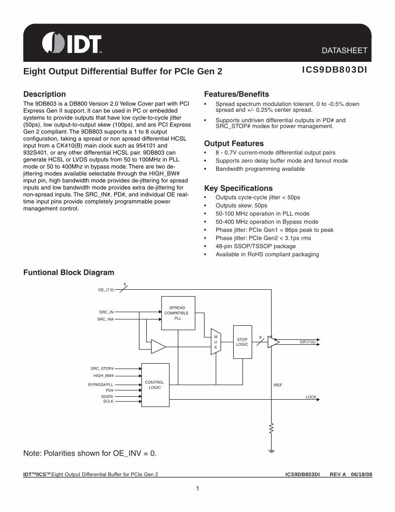
STOPLOGIC
SRC_IN
SRC_IN#
DIF(7:0))
CONTROLLOGIC
BYPASS#/PLL
SDATASCLK
PD#
SPREADCOMPATIBLE
PLL
8
IREF
OE_(7:0)
8
LOCK
SRC_STOP#
HIGH_BW#
MUX
Description
Output Features
The 9DB803 is a DB800 Version 2.0 Yellow Cover part with PCIExpress Gen II support. It can be used in PC or embeddedsystems to provide outputs that have low cycle-to-cycle jitter(50ps), low output-to-output skew (100ps), and are PCI ExpressGen 2 compliant. The 9DB803 supports a 1 to 8 outputconfiguration, taking a spread or non spread differential HCSLinput from a CK410(B) main clock such as 954101 and932S401, or any other differential HCSL pair. 9DB803 cangenerate HCSL or LVDS outputs from 50 to 100MHz in PLLmode or 50 to 400Mhz in bypass mode. There are two de-jittering modes available selectable through the HIGH_BW#input pin, high bandwidth mode provides de-jittering for spreadinputs and low bandwidth mode provides extra de-jittering fornon-spread inputs. The SRC_IN#, PD#, and individual OE real-time input pins provide completely programmable powermanagement control.
• 8 - 0.7V current-mode differential output pairs• Supports zero delay buffer mode and fanout mode• Bandwidth programming available
Funtional Block Diagram
Key Specifications• Outputs cycle-cycle jitter < 50ps• Outputs skew: 50ps• 50-100 MHz operation in PLL mode• 50-400 MHz operation in Bypass mode• Phase jitter: PCIe Gen1 < 86ps peak to peak• Phase jitter: PCIe Gen2 < 3.1ps rms• 48-pin SSOP/TSSOP package• Available in RoHS compliant packaging
Features/Benefits• Spread spectrum modulation tolerant, 0 to -0.5% down
spread and +/- 0.25% center spread.
• Supports undriven differential outputs in PD# andSRC_STOP# modes for power management.
Note: Polarities shown for OE_INV = 0.
IDTTM/ICSTM Eight Output Differential Buffer for PCIe Gen 2 ICS9DB803DI REV A 06/18/08
ICS9DB803DIEight Output Differential Buffer for PCIe for Gen 2
2
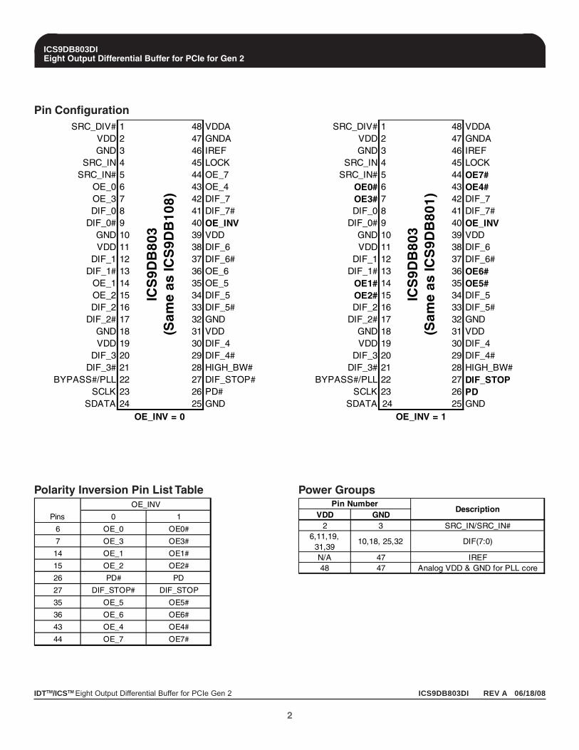
Pin Configuration
Polarity Inversion Pin List Table
SRC_DIV# 1 48 VDDAVDD 2 47 GNDAGND 3 46 IREF
SRC_IN 4 45 LOCKSRC_IN# 5 44 OE_7
OE_0 6 43 OE_4OE_3 7 42 DIF_7DIF_0 8 41 DIF_7#
DIF_0# 9 40 OE_INVGND 10 39 VDDVDD 11 38 DIF_6
DIF_1 12 37 DIF_6#DIF_1# 13 36 OE_6
OE_1 14 35 OE_5OE_2 15 34 DIF_5DIF_2 16 33 DIF_5#
DIF_2# 17 32 GNDGND 18 31 VDDVDD 19 30 DIF_4
DIF_3 20 29 DIF_4#DIF_3# 21 28 HIGH_BW#
BYPASS#/PLL 22 27 DIF_STOP#SCLK 23 26 PD#
SDATA 24 25 GNDOE_INV = 0
ICS
9DB
803
(Sam
e as
ICS
9DB
108)
SRC_DIV# 1 48 VDDAVDD 2 47 GNDAGND 3 46 IREF
SRC_IN 4 45 LOCKSRC_IN# 5 44 OE7#
OE0# 6 43 OE4#OE3# 7 42 DIF_7DIF_0 8 41 DIF_7#
DIF_0# 9 40 OE_INVGND 10 39 VDDVDD 11 38 DIF_6
DIF_1 12 37 DIF_6#DIF_1# 13 36 OE6#
OE1# 14 35 OE5#OE2# 15 34 DIF_5DIF_2 16 33 DIF_5#
DIF_2# 17 32 GNDGND 18 31 VDDVDD 19 30 DIF_4
DIF_3 20 29 DIF_4#DIF_3# 21 28 HIGH_BW#
BYPASS#/PLL 22 27 DIF_STOPSCLK 23 26 PD
SDATA 24 25 GNDOE_INV = 1
ICS
9DB
803
(Sam
e as
ICS
9DB
801)
0 1
6 OE_0 OE0#
7 OE_3 OE3#
14 OE_1 OE1#
15 OE_2 OE2#
26 PD# PD
27 DIF_STOP# DIF_STOP
35 OE_5 OE5#
36 OE_6 OE6#
43 OE_4 OE4#
44 OE_7 OE7#
Pins
OE_INVVDD GND
2 3 SRC_IN/SRC_IN#6,11,19,
31,3910,18, 25,32 DIF(7:0)
N/A 47 IREF48 47 Analog VDD & GND for PLL core
DescriptionPin Number
Power Groups

IDTTM/ICSTM Eight Output Differential Buffer for PCIe Gen 2 ICS9DB803DI REV A 06/18/08
ICS9DB803DIEight Output Differential Buffer for PCIe for Gen 2
3
Pin Description for OE_INV = 0PIN # PIN NAME PIN TYPE DESCRIPTION
1 SRC_DIV# INActive low Input for determining SRC output frequency SRC or SRC/2. 0 = SRC/2, 1= SRC
2 VDD PWR Power supply, nominal 3.3V
3 GND PWR Ground pin.
4 SRC_IN IN 0.7 V Differential SRC TRUE input
5 SRC_IN# IN 0.7 V Differential SRC COMPLEMENTARY input
6 OE_0 INActive high input for enabling output 0. 0 = tri-state outputs, 1= enable outputs
7 OE_3 INActive high input for enabling output 3.0 = tri-state outputs, 1= enable outputs
8 DIF_0 OUT 0.7V differential true clock output9 DIF_0# OUT 0.7V differential complement clock output
10 GND PWR Ground pin.
11 VDD PWR Power supply, nominal 3.3V
12 DIF_1 OUT 0.7V differential true clock output
13 DIF_1# OUT 0.7V differential complement clock output
14 OE_1 INActive high input for enabling output 1. 0 = tri-state outputs, 1= enable outputs
15 OE_2 INActive high input for enabling output 2.0 = tri-state outputs, 1= enable outputs
16 DIF_2 OUT 0.7V differential true clock output
17 DIF_2# OUT 0.7V differential complement clock output18 GND PWR Ground pin.
19 VDD PWR Power supply, nominal 3.3V
20 DIF_3 OUT 0.7V differential true clock output
21 DIF_3# OUT 0.7V differential complement clock output
22 BYPASS#/PLL INInput to select Bypass(fan-out) or PLL (ZDB) mode0 = Bypass mode, 1= PLL mode
23 SCLK IN Clock pin of SMBus circuitry, 5V tolerant. 24 SDATA I/O Data pin for SMBus circuitry, 5V tolerant.

IDTTM/ICSTM Eight Output Differential Buffer for PCIe Gen 2 ICS9DB803DI REV A 06/18/08
ICS9DB803DIEight Output Differential Buffer for PCIe for Gen 2
4
Pin Description for OE_INV = 0PIN # PIN NAME PIN TYPE DESCRIPTION
25 GND PWR Ground pin.
26 PD# INAsynchronous active low input pin used to power down the device. The internal clocks are disabled and the VCO and the crystal are stopped.
27 DIF_STOP# IN Active low input to stop differential output clocks.
28 HIGH_BW# PWR3.3V input for selecting PLL Band Width0 = High, 1= Low
29 DIF_4# OUT 0.7V differential complement clock output
30 DIF_4 OUT 0.7V differential true clock output
31 VDD PWR Power supply, nominal 3.3V
32 GND PWR Ground pin.33 DIF_5# OUT 0.7V differential complement clock output34 DIF_5 OUT 0.7V differential true clock output
35 OE_5 INActive high input for enabling output 5. 0 = tri-state outputs, 1= enable outputs
36 OE_6 INActive high input for enabling output 6. 0 = tri-state outputs, 1= enable outputs
37 DIF_6# OUT 0.7V differential complement clock output
38 DIF_6 OUT 0.7V differential true clock output
39 VDD PWR Power supply, nominal 3.3V
40 OE_INV INThis latched input selects the polarity of the OE pins.0 = OE pins active high, 1 = OE pins active low (OE#)
41 DIF_7# OUT 0.7V differential complement clock output42 DIF_7 OUT 0.7V differential true clock output
43 OE_4 INActive high input for enabling output 4. 0 = tri-state outputs, 1= enable outputs
44 OE_7 INActive high input for enabling output 7. 0 = tri-state outputs, 1= enable outputs
45 LOCK OUT3.3V output indicating PLL Lock Status. This pin goes high when lock is achieved.
46 IREF IN
This pin establishes the reference current for the differential current-mode output pairs. This pin requires a fixed precision resistor tied to ground in order to establish the appropriate current. 475 ohms is the standard value.
47 GNDA PWR Ground pin for the PLL core.48 VDDA PWR 3.3V power for the PLL core.

IDTTM/ICSTM Eight Output Differential Buffer for PCIe Gen 2 ICS9DB803DI REV A 06/18/08
ICS9DB803DIEight Output Differential Buffer for PCIe for Gen 2
5
Pin Description for OE_INV = 1PIN # PIN NAME PIN TYPE DESCRIPTION
1 SRC_DIV# INActive low Input for determining SRC output frequency SRC or SRC/2. 0 = SRC/2, 1= SRC
2 VDD PWR Power supply, nominal 3.3V
3 GND PWR Ground pin.
4 SRC_IN IN 0.7 V Differential SRC TRUE input
5 SRC_IN# IN 0.7 V Differential SRC COMPLEMENTARY input
6 OE0# INActive low input for enabling DIF pair 0. 1 = tri-state outputs, 0 = enable outputs
7 OE3# INActive low input for enabling DIF pair 3. 1 = tri-state outputs, 0 = enable outputs
8 DIF_0 OUT 0.7V differential true clock output9 DIF_0# OUT 0.7V differential complement clock output
10 GND PWR Ground pin.
11 VDD PWR Power supply, nominal 3.3V
12 DIF_1 OUT 0.7V differential true clock output
13 DIF_1# OUT 0.7V differential complement clock output
14 OE1# INActive low input for enabling DIF pair 1. 1 = tri-state outputs, 0 = enable outputs
15 OE2# INActive low input for enabling DIF pair 2. 1 = tri-state outputs, 0 = enable outputs
16 DIF_2 OUT 0.7V differential true clock output
17 DIF_2# OUT 0.7V differential complement clock output18 GND PWR Ground pin.
19 VDD PWR Power supply, nominal 3.3V
20 DIF_3 OUT 0.7V differential true clock output
21 DIF_3# OUT 0.7V differential complement clock output
22 BYPASS#/PLL INInput to select Bypass(fan-out) or PLL (ZDB) mode0 = Bypass mode, 1= PLL mode
23 SCLK IN Clock pin of SMBus circuitry, 5V tolerant. 24 SDATA I/O Data pin for SMBus circuitry, 5V tolerant.

IDTTM/ICSTM Eight Output Differential Buffer for PCIe Gen 2 ICS9DB803DI REV A 06/18/08
ICS9DB803DIEight Output Differential Buffer for PCIe for Gen 2
6
Pin Description for OE_INV = 1PIN # PIN NAME PIN TYPE DESCRIPTION
25 GND PWR Ground pin.
26 PD INAsynchronous active high input pin used to power down the device. The internal clocks are disabled and the VCO is stopped.
27 DIF_STOP IN Active High input to stop differential output clocks.
28 HIGH_BW# PWR3.3V input for selecting PLL Band Width0 = High, 1= Low
29 DIF_4# OUT 0.7V differential complement clock output
30 DIF_4 OUT 0.7V differential true clock output
31 VDD PWR Power supply, nominal 3.3V
32 GND PWR Ground pin.33 DIF_5# OUT 0.7V differential complement clock output34 DIF_5 OUT 0.7V differential true clock output
35 OE5# INActive low input for enabling DIF pair 5. 1 = tri-state outputs, 0 = enable outputs
36 OE6# INActive low input for enabling DIF pair 6. 1 = tri-state outputs, 0 = enable outputs
37 DIF_6# OUT 0.7V differential complement clock output
38 DIF_6 OUT 0.7V differential true clock output
39 VDD PWR Power supply, nominal 3.3V
40 OE_INV INThis latched input selects the polarity of the OE pins.0 = OE pins active high, 1 = OE pins active low (OE#)
41 DIF_7# OUT 0.7V differential complement clock output42 DIF_7 OUT 0.7V differential true clock output
43 OE4# INActive low input for enabling DIF pair 4 1 = tri-state outputs, 0 = enable outputs
44 OE7# INActive low input for enabling DIF pair 7. 1 = tri-state outputs, 0 = enable outputs
45 LOCK OUT3.3V output indicating PLL Lock Status. This pin goes high when lock is achieved.
46 IREF IN
This pin establishes the reference current for the differential current-mode output pairs. This pin requires a fixed precision resistor tied to ground in order to establish the appropriate current. 475 ohms is the standard value.
47 GNDA PWR Ground pin for the PLL core.48 VDDA PWR 3.3V power for the PLL core.
IDTTM/ICSTM Eight Output Differential Buffer for PCIe Gen 2 ICS9DB803DI REV A 06/18/08
ICS9DB803DIEight Output Differential Buffer for PCIe for Gen 2
7
Absolute Max
Electrical Characteristics - Input/Supply/Common Output ParametersTA = -40 - 85°C; Supply Voltage VDD = 3.3 V +/-5%
PARAMETER SYMBOL CONDITIONS MIN TYP MAX UNITS NOTES
Input High Voltage VIH 3.3 V +/-5% 2 VDD + 0.3 V
Input Low Voltage VIL 3.3 V +/-5% GND - 0.3 0.8 V
Input High Current IIH VIN = VDD -5 5 uA
IIL1 VIN = 0 V; Inputs with no pull-up resistors -5 uA
IIL2 VIN = 0 V; Inputs with pull-up resistors -200 uA
Operating Supply Current IDD3.3OP Full Active, CL = Full load; 200 mA
all diff pairs driven 60 mAall differential pairs tri-stated 6 mA
FiPLL PLL Mode 50 110 MHz 1
FiBYPASS Bypass Mode 50 400 MHz 1
Pin Inductance Lpin 7 nH 1
CIN Logic Inputs 1.5 5 pF 1
COUT Output pin capacitance 6 pF 1PLL Bandwidth when PLL_BW=0 2 3 4 MHz 1PLL Bandwidth when PLL_BW=1 0.7 1 1.4 MHz 1
Clk Stabilization TSTAB
From VDD Power-Up and after input clock stabilization or de-assertion of PD# to 1st
clock1 ms 1,2
Modulation Frequency fMOD Triangular Modulation 30 33 kHz 1
Tdrive_SRC_STOP# tDRVSTPDIF output enable after
SRC_Stop# de-assertion10 ns 1,3
Tdrive_PD# tDRVPDDIF output enable after
PD# de-assertion300 us 1,3
Tfall tF Fall time of PD# and SRC_STOP# 5 ns 1
Trise tR Rise time of PD# and SRC_STOP# 5 ns 21Guaranteed by design and characterization, not 100% tested in production.2See timing diagrams for timing requirements.
IDD3.3PD
3Time from deassertion until outputs are >200 mV
Capacitance
Input Low Current
Powerdown Current
PLL Bandwidth BW
Input Frequency
Symbol Parameter Min Max UnitsVDD_A 3.3V Core Supply Voltage 4.6 VVDD_In 3.3V Logic Supply Voltage 4.6 V
VIL Input Low Voltage GND-0.5 V
VIH Input High Voltage VDD+0.5V V
Ts Storage Temperature -65 150 °CTambient Ambient Operating Temp -40 85 °C
Tcase Case Temperature 115 °C
ESD protInput ESD protectionhuman body model 2000 V
IDTTM/ICSTM Eight Output Differential Buffer for PCIe Gen 2 ICS9DB803DI REV A 06/18/08
ICS9DB803DIEight Output Differential Buffer for PCIe for Gen 2
8
Electrical Characteristics - Clock Input ParametersTA = -40 - 85°C; Supply Voltage VDD = 3.3 V +/-5%
PARAMETER SYMBOL CONDITIONS MIN TYP MAX UNITS NOTES
Input High Voltage - DIF_IN
VIHDIFDifferential inputs
(single-ended measurement)600 800 1150 mV 1
Input Low Voltage - DIF_IN
VILDIFDifferential inputs
(single-ended measurement)VSS - 300 0 300 mV 1
Input Common Mode Voltage - DIF_IN
VCOM Common Mode Input Voltage 300 1000 mV 1
Input Amplitude - DIF_IN VSWING Peak to Peak value 300 1450 mV 1
Input Slew Rate - DIF_IN dv/dt Measured differentially 0.4 8 V/ns 1,2
Input Leakage Current IIN VIN = VDD , VIN = GND -5 5 uA 1
Input Duty Cycle dtin Measurement from differential wavefrom 45 55 % 1Input Jitter - Cycle to
CycleJDIFIn Differential Measurement 0 125 ps 1
1 Guaranteed by design and characterization, not 100% tested in production.2Slew rate measured through Vswing min centered around differential zero
IDTTM/ICSTM Eight Output Differential Buffer for PCIe Gen 2 ICS9DB803DI REV A 06/18/08
ICS9DB803DIEight Output Differential Buffer for PCIe for Gen 2
9
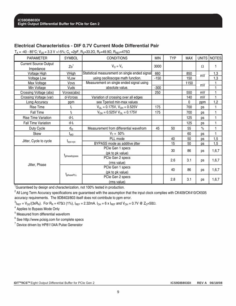
Electrical Characteristics - DIF 0.7V Current Mode Differential PairTA = -40 - 85°C; VDD = 3.3 V +/-5%; CL =2pF, RS=33.2Ω, RP=49.9Ω, RREF=475Ω
PARAMETER SYMBOL CONDITIONS MIN TYP MAX UNITS NOTES
Current Source Output Impedance Zo1 VO = Vx 3000 Ω 1
Voltage High VHigh 660 850 1,3Voltage Low VLow -150 150 1,3Max Voltage Vovs 1150 1Min Voltage Vuds -300 1
Crossing Voltage (abs) Vcross(abs) 250 550 mV 1Crossing Voltage (var) d-Vcross Variation of crossing over all edges 140 mV 1
Long Accuracy ppm see Tperiod min-max values 0 ppm 1,2Rise Time tr VOL = 0.175V, VOH = 0.525V 175 700 ps 1Fall Time tf VOH = 0.525V VOL = 0.175V 175 700 ps 1
Rise Time Variation d-tr 125 ps 1Fall Time Variation d-tf 125 ps 1
Duty Cycle dt3 Measurement from differential wavefrom 45 50 55 % 1Skew tsk3 VT = 50% 60 ps 1
PLL mode 40 50 ps 1,5BYPASS mode as additive jitter 15 50 ps 1,5
PCIe Gen 1 specs(pk to pk value)
30 86 ps 1,6,7
PCIe Gen 2 specs (rms value)
2.6 3.1 ps 1,6,7
PCIe Gen 1 specs(pk to pk value)
40 86 ps 1,6,7
PCIe Gen 2 specs (rms value)
2.8 3.1 ps 1,6,7
1Guaranteed by design and characterization, not 100% tested in production.
3IREF = VDD/(3xRR). For RR = 475Ω (1%), IREF = 2.32mA. IOH = 6 x IREF and VOH = 0.7V @ ZO=50Ω.4 Applies to Bypass Mode Only5 Measured from differential waveform6 See http://www.pcisig.com for complete specs7 Device driven by HP81134A Pulse Generator
2 All Long Term Accuracy specifications are guaranteed with the assumption that the input clock complies with CK409/CK410/CK505 accuracy requirements. The 9DB403/803 itself does not contribute to ppm error.
tjphasePLL
Jitter, Cycle to cycle tjcyc-cyc
tjphasebypass
Jitter, Phase
Statistical measurement on single ended signal using oscilloscope math function.
mV
Measurement on single ended signal using absolute value.
mV

IDTTM/ICSTM Eight Output Differential Buffer for PCIe Gen 2 ICS9DB803DI REV A 06/18/08
ICS9DB803DIEight Output Differential Buffer for PCIe for Gen 2
10
Clock Periods Differential Outputs with Spread Spectrum Enabled
1 Clock 1us 0.1s 0.1s 0.1s 1us 1 ClockLg- -SSC -ppm error 0ppm + ppm error +SSC Lg+
Absolute Period
Short-term Average
Long-Term Average
PeriodLong-Term
AverageShort-term
AveragePeriod
Minimum Absolute
Period
Minimum Absolute
Period
Minimum Absolute
PeriodNominal Maximum Maximum Maximum
DIF 100 9.87400 9.99900 9.99900 10.00000 10.00100 10.05130 10.17630 ns 1,2,3
DIF 133 7.41425 7.49925 7.49925 7.50000 7.50075 7.53845 7.62345 ns 1,2,4
DIF 166 5.91440 5.99940 5.99940 6.00000 6.00060 6.03076 6.11576 ns 1,2,4
DIF 200 4.91450 4.99950 4.99950 5.00000 5.00050 5.02563 5.11063 ns 1,2,4
DIF 266 3.66463 3.74963 3.74963 3.75000 3.75038 3.76922 3.85422 ns 1,2,4
DIF 333 2.91470 2.99970 2.99970 3.00000 3.00030 3.01538 3.10038 ns 1,2,4
DIF 400 2.41475 2.49975 2.49975 2.50000 2.50025 2.51282 2.59782 ns 1,2,4
Clock Periods Differential Outputs with Spread Spectrum Disabled
1 Clock 1us 0.1s 0.1s 0.1s 1us 1 ClockLg- -SSC -ppm error 0ppm + ppm error +SSC Lg+
Absolute Period
Short-term Average
Long-Term Average
PeriodLong-Term
AverageShort-term
AveragePeriod
Minimum Absolute
Period
Minimum Absolute
Period
Minimum Absolute
PeriodNominal Maximum Maximum Maximum
DIF 100 9.87400 9.99900 10.00000 10.00100 10.17630 ns 1,2,3
DIF 133 7.41425 7.49925 7.50000 7.50075 7.62345 ns 1,2,4
DIF 166 5.91440 5.99940 6.00000 6.00060 6.11576 ns 1,2,4
DIF 200 4.91450 4.99950 5.00000 5.00050 5.11063 ns 1,2,4
DIF 266 3.66463 3.74963 3.75000 3.75038 3.85422 ns 1,2,4
DIF 333 2.91470 2.99970 3.00000 3.00030 3.10038 ns 1,2,4
DIF 400 2.41475 2.49975 2.50000 2.50025 2.59782 ns 1,2,41Guaranteed by design and characterization, not 100% tested in production.
3 Driven by SRC output of main clock, PLL or Bypass mode4 Driven by CPU output of CK410/CK505 main clock, Bypass mode only
Definition
Units
Sig
nal N
ame
Sig
nal N
ame
Measurement WindowSymbol
2 All Long Term Accuracy specifications are guaranteed with the assumption that the input clock complies with CK409/CK410/CK505 accuracy requirements. The 9DB403/803 itself does not contribute to ppm error.
Notes
Notes
Definition
Measurement Window
Units
Symbol

IDTTM/ICSTM Eight Output Differential Buffer for PCIe Gen 2 ICS9DB803DI REV A 06/18/08
ICS9DB803DIEight Output Differential Buffer for PCIe for Gen 2
11
SRC Reference Clock
Common Recommendations for Differential Routing Dimension or Value Unit Figure L1 length, Route as non-coupled 50 ohm trace. 0.5 max inch 1 L2 length, Route as non-coupled 50 ohm trace. 0.2 max inch 1 L3 length, Route as non-coupled 50 ohm trace. 0.2 max inch 1 Rs 33 ohm 1Rt 49.9 ohm 1
Down Device Differential Routing Dimension or Value Unit Figure L4 length, Route as coupled microstrip 100 ohm differential trace. 2 min to 16 max inch 1 L4 length, Route as coupled stripline 100 ohm differential trace. 1.8 min to 14.4 max inch 1
Differential Routing to PCI Express Connector Dimension or Value Unit Figure L4 length, Route as coupled microstrip 100 ohm differential trace. 0.25 to 14 max inch 2 L4 length, Route as coupled stripline 100 ohm differential trace. 0.225 min to 12.6 max inch 2
Figure 1 Down device routing.
Rs
Rs
Rt Rt
HSCL OutputBuffer
PCI Ex BoardDown Device
REF_CLK Input
L1 L2
L3’
L4
L1’ L2’
L3
L4’
Figure 1
Figure 2 PCI Express Connector Routing.
Rs
Rs
Rt Rt
HSCL OutputBuffer
PCI ExAdd In Board
REF_CLK Input
L1 L2
L3’
L4
L1’ L2’
L3
L4’
Figure 2

IDTTM/ICSTM Eight Output Differential Buffer for PCIe Gen 2 ICS9DB803DI REV A 06/18/08
ICS9DB803DIEight Output Differential Buffer for PCIe for Gen 2
12
Alternative termination for LVDS and other common differential signals. Figure 3. Vdiff Vp-p Vcm R1 R2 R3 R4 Note 0.45 v 0.22v 1.08 33 150 100 100 0.58 0.28
0.3
0.6 33 78.7 137 100 0.80 0.40 0.6 33 78.7 none 100 ICS874003i-02 input compatible 0.60 1.2 33 174 140 100 Standard LVDS R1a = R1b = R1
R2a = R2b = R2 Cable connected AC coupled application, figure 4
Component Value Note R5a,R5b 5% R6a,R6b Cc 0.1
0.350
Vcm volts
Figure_3.
R1b
R1a
R2a R2b
HSCL OutputBuffer
Down DeviceREF_CLK Input
L1 L2
L3’
L4
L1’ L2’
L3
L4’
R3 R4
Figure_4.
PCIe DeviceREF_CLK Input
L4
L4’
R6b
R5b
R6a
R5a
3.3 Volts
Cc
Cc
8.2K5%uF
1K

IDTTM/ICSTM Eight Output Differential Buffer for PCIe Gen 2 ICS9DB803DI REV A 06/18/08
ICS9DB803DIEight Output Differential Buffer for PCIe for Gen 2
13
General SMBus serial interface information for the ICS9DB803DI
How to Write:• Controller (host) sends a start bit.• Controller (host) sends the write address DC (h)
• ICS clock will acknowledge• Controller (host) sends the begining byte location = N• ICS clock will acknowledge• Controller (host) sends the data byte count = X• ICS clock will acknowledge• Controller (host) starts sending Byte N through
Byte N + X -1• ICS clock will acknowledge each byte one at a time• Controller (host) sends a Stop bit
How to Read:• Controller (host) will send start bit.• Controller (host) sends the write address DC
(h)
• ICS clock will acknowledge• Controller (host) sends the begining byte
location = N• ICS clock will acknowledge• Controller (host) will send a separate start bit.• Controller (host) sends the read address DD (h)
• ICS clock will acknowledge• ICS clock will send the data byte count = X• ICS clock sends Byte N + X -1• ICS clock sends Byte 0 through byte X (if X(h)
was written to byte 8).• Controller (host) will need to acknowledge each byte• Controllor (host) will send a not acknowledge bit• Controller (host) will send a stop bit
ICS (Slave/Receiver)T
WRACK
ACK
ACK
ACK
ACKP stoP bit
X B
yte
Index Block Write Operation
Slave Address DC(h)
Beginning Byte = N
WRite
starT bitController (Host)
Byte N + X - 1
Data Byte Count = X
Beginning Byte N
T starT bit
WR WRite
RT Repeat starT
RD ReaD
Beginning Byte N
Byte N + X - 1N Not acknowledgeP stoP bit
Slave Address DD(h)
Index Block Read Operation
Slave Address DC(h)
Beginning Byte = NACK
ACK
Data Byte Count = X
ACK
ICS (Slave/Receiver)Controller (Host)
X B
yte
ACK
ACK

IDTTM/ICSTM Eight Output Differential Buffer for PCIe Gen 2 ICS9DB803DI REV A 06/18/08
ICS9DB803DIEight Output Differential Buffer for PCIe for Gen 2
14
SMBus Table: Frequency Select Register, READ/WRITE ADDRESS (DC/DD)Pin # Name Control Function Type 0 1 PWD
Bit 7 PD_Mode PD# drive mode RW driven Hi-Z 0Bit 6 STOP_Mode SRC_Stop# drive mode RW driven Hi-Z 0Bit 5 PD_Polarity Select PD polarity RW Low High 0Bit 4 Reserved Reserved RW XBit 3 Reserved Reserved RW XBit 2 PLL_BW# Select PLL BW RW High BW Low BW 1Bit 1 BYPASS# BYPASS#/PLL RW fan-out ZDB 1Bit 0 SRC_DIV# SRC Divide by 2 Select RW x/2 1x 1
SMBus Table: Output Control RegisterPin # Name Control Function Type 0 1 PWD
Bit 7 DIF_7 Output Control RW Disable Enable 1Bit 6 DIF_6 Output Control RW Disable Enable 1Bit 5 DIF_5 Output Control RW Disable Enable 1Bit 4 DIF_4 Output Control RW Disable Enable 1Bit 3 DIF_3 Output Control RW Disable Enable 1Bit 2 DIF_2 Output Control RW Disable Enable 1Bit 1 DIF_1 Output Control RW Disable Enable 1Bit 0 DIF_0 Output Control RW Disable Enable 1
SMBus Table: Output Control RegisterPin # Name Control Function Type 0 1 PWD
Bit 7 DIF_7 Output Control RW Free-run Stoppable 0Bit 6 DIF_6 Output Control RW Free-run Stoppable 0Bit 5 DIF_5 Output Control RW Free-run Stoppable 0Bit 4 DIF_4 Output Control RW Free-run Stoppable 0Bit 3 DIF_3 Output Control RW Free-run Stoppable 0Bit 2 DIF_2 Output Control RW Free-run Stoppable 0Bit 1 DIF_1 Output Control RW Free-run Stoppable 0Bit 0 DIF_0 Output Control RW Free-run Stoppable 0
SMBus Table: Output Control RegisterPin # Name Control Function Type 0 1 PWD
Bit 7 RW XBit 6 RW XBit 5 RW XBit 4 RW XBit 3 RW XBit 2 RW XBit 1 RW XBit 0 RW X
Reserved Reserved
Reserved ReservedReserved Reserved
Reserved ReservedReserved Reserved
Reserved ReservedReserved Reserved
Reserved Reserved
12,138,9
Byte 3
34,3330,2920,2116,17
8,9
Byte 242,4138,37
30,2920,2116,1712,13
Byte 142,4138,3734,33
--
- Reserved-
-- Reserved
Byte 0--
IDTTM/ICSTM Eight Output Differential Buffer for PCIe Gen 2 ICS9DB803DI REV A 06/18/08
ICS9DB803DIEight Output Differential Buffer for PCIe for Gen 2
15
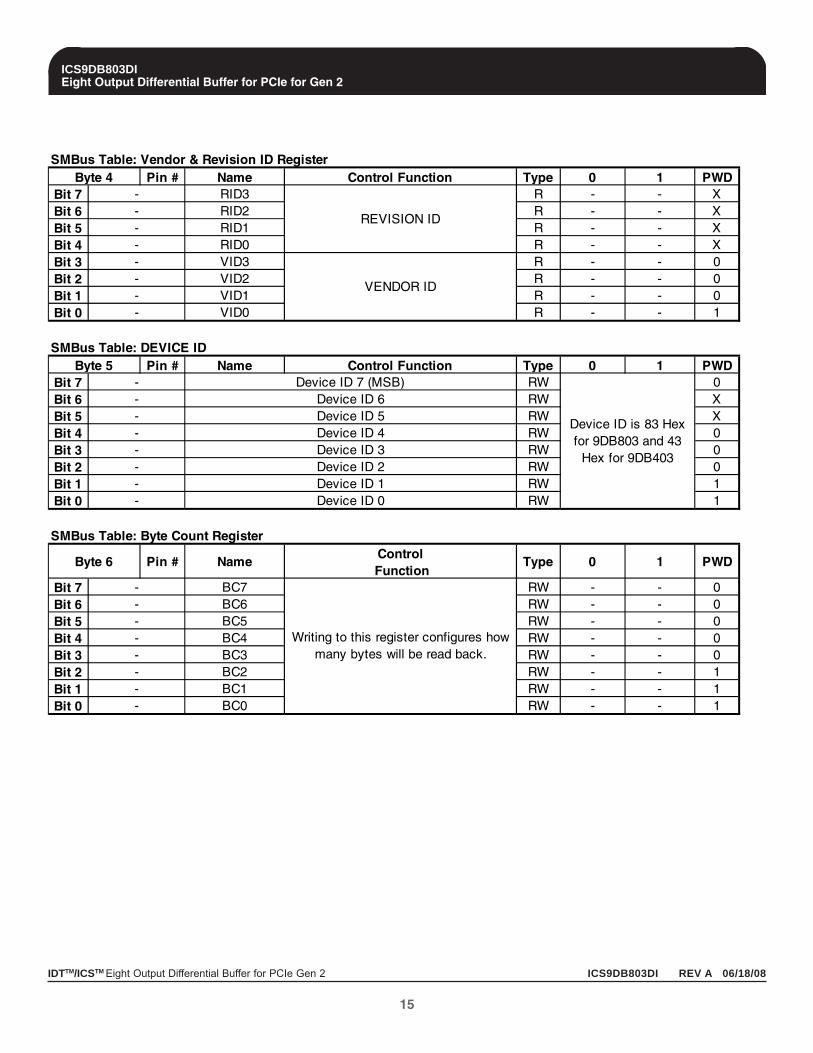
SMBus Table: Vendor & Revision ID RegisterPin # Name Control Function Type 0 1 PWD
Bit 7 RID3 R - - XBit 6 RID2 R - - XBit 5 RID1 R - - XBit 4 RID0 R - - XBit 3 VID3 R - - 0Bit 2 VID2 R - - 0Bit 1 VID1 R - - 0Bit 0 VID0 R - - 1
SMBus Table: DEVICE IDPin # Name Control Function Type 0 1 PWD
Bit 7 RW 0Bit 6 RW XBit 5 RW XBit 4 RW 0Bit 3 RW 0Bit 2 RW 0Bit 1 RW 1Bit 0 RW 1
SMBus Table: Byte Count Register
Pin # NameControl
FunctionType 0 1 PWD
Bit 7 BC7 RW - - 0Bit 6 BC6 RW - - 0Bit 5 BC5 RW - - 0Bit 4 BC4 RW - - 0Bit 3 BC3 RW - - 0Bit 2 BC2 RW - - 1Bit 1 BC1 RW - - 1Bit 0 BC0 RW - - 1
Device ID 1
Device ID 6Device ID 7 (MSB)
Device ID is 83 Hex for 9DB803 and 43
Hex for 9DB403
Device ID 5Device ID 4Device ID 3
Device ID 0
Device ID 2
Byte 6
-
Writing to this register configures how many bytes will be read back.
-------
Byte 5---
-
----
-
VENDOR ID---
Byte 4-
REVISION ID---

IDTTM/ICSTM Eight Output Differential Buffer for PCIe Gen 2 ICS9DB803DI REV A 06/18/08
ICS9DB803DIEight Output Differential Buffer for PCIe for Gen 2
16
The PD# pin cleanly shuts off all clocks and places the device into a power saving mode. PD# must be asserted before shuttingoff the input clock or power to insure an orderly shutdown. PD is asynchronous active-low input for both powering down thedevice and powering up the device. When PD# is asserted, all clocks will be driven high, or tri-stated (depending on the PD#drive mode and Output control bits) before the PLL is shut down.
PD#, Power Down
When PD# is sampled low by two consecutive rising edges of DIF#, all DIF outputs must be held High, or tri-stated (dependingon the PD# drive mode and Output control bits) on the next High-Low transition of the DIF# outputs. When the PD# drive modebit is set to ‘0’, all clock outputs will be held with DIF driven High with 2 x IREF and DIF# tri-stated. If the PD# drive mode bit isset to ‘1’, both DIF and DIF# are tri-stated.
PD# Assertion
Power-up latency is less than 1 ms. This is the time from de-assertion of the PD# pin, or VDD reaching 3.3V, or the time fromvalid SRC_IN clocks until the time that stable clocks are output from the device (PLL Locked). If the PD# drive mode bit is setto ‘1’, all the DIF outputs must driven to a voltage of >200 mV within 300 us of PD# de-assertion.
PD# De-assertion
PWRDWN#
DIF
DIF#
PWRDWN#
DIF
DIF#
Tstable<1mS
Tdrive_PwrDwn#<300uS, >200mV
Note: Polarities in timing diagrams are shown OE_INV = 0. They are similar to OE_INV = 1.

IDTTM/ICSTM Eight Output Differential Buffer for PCIe Gen 2 ICS9DB803DI REV A 06/18/08
ICS9DB803DIEight Output Differential Buffer for PCIe for Gen 2
17
Asserting SRC_STOP# causes all DIF outputs to stop after their next transition (if the control register settings allow the outputto stop). When the SRC_STOP# drive bit is ‘0’, the final state of all stopped DIF outputs is DIF = High and DIF# = Low. Thereis no change in output drive current. DIF is driven with 6xIREF. DIF# is not driven, but pulled low by the termination. When theSRC_STOP# drive bit is ‘1’, the final state of all DIF output pins is Low. Both DIF and DIF# are not driven.
SRC_STOP# - Assertion
All stopped differential outputs resume normal operation in a glitch-free manner. The de-assertion latency to active outputs is2-6 DIF clock periods, with all DIF outputs resuming simultaneously. If the SRC_STOP# drive control bit is ‘1’ (tri-state), allstopped DIF outputs must be driven High (>200 mV) within 10 ns of de-assertion.
SRC_STOP# - De-assertion (transition from '0' to '1')
The SRC_STOP# signal is an active-low asynchronous input that cleanly stops and starts the DIF outputs. A valid clock mustbe present on SRC_IN for this input to work properly. The SRC_STOP# signal is de-bounced and must remain stable for twoconsecutive rising edges of DIF# to be recognized as a valid assertion or de-assertion.
SRC_STOP#
PWRDWN#
SRC_Stop#
DIF (Free Running)
DIF# (Free Running)
DIF (Stoppable)
DIF# (Stoppable)
1mS
PWRDWN#
SRC_Stop#
DIF (Free Running)
DIF# (Free Running)
DIF (Stoppable)
DIF# (Stoppable)
1mS
SRC_STOP_1 (SRC_Stop = Driven, PD = Driven)
SRC_STOP_2 (SRC_Stop =Tristate, PD = Driven)

IDTTM/ICSTM Eight Output Differential Buffer for PCIe Gen 2 ICS9DB803DI REV A 06/18/08
ICS9DB803DIEight Output Differential Buffer for PCIe for Gen 2
18
PWRDWN#
SRC_Stop#
DIF (Free Running)
DIF# (Free Running)
DIF (Stoppable)
DIF# (Stoppable)
1mS
PWRDWN#
SRC_Stop#
DIF (Free Running)
DIF# (Free Running)
DIF (Stoppable)
DIF# (Stoppable)
1mS
SRC_STOP_4 (SRC_Stop = Tristate, PD = Tristate)
SRC_STOP_3 (SRC_Stop = Driven, PD = Tristate)
IDTTM/ICSTM Eight Output Differential Buffer for PCIe Gen 2 ICS9DB803DI REV A 06/18/08
ICS9DB803DIEight Output Differential Buffer for PCIe for Gen 2
19
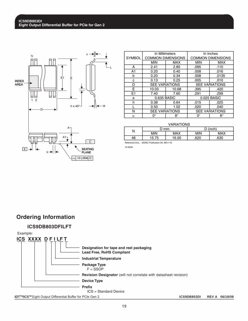
INDEXAREAINDEXAREA
1 2
N
Dh x 45°
E1 E
α
SEATINGPLANESEATINGPLANE
A1
A
e
- C -
b
.10 (.004) C.10 (.004) C
c
L
MIN MAX MIN MAXA 2.41 2.80 .095 .110
A1 0.20 0.40 .008 .016b 0.20 0.34 .008 .0135c 0.13 0.25 .005 .010DE 10.03 10.68 .395 .420
E1 7.40 7.60 .291 .299eh 0.38 0.64 .015 .025L 0.50 1.02 .020 .040Nα 0° 8° 0° 8°
MIN MAX MIN MAX48 15.75 16.00 .620 .630
10-0034
SYMBOLIn Millimeters In Inches
COMMON DIMENSIONS COMMON DIMENSIONS
SEE VARIATIONS SEE VARIATIONS
0.635 BASIC 0.025 BASIC
Reference Doc.: JEDEC Publication 95, MO-118
VARIATIONS
SEE VARIATIONS SEE VARIATIONS
ND mm. D (inch)
Ordering Information
ICS9DB803DFILFTExample:
Designation for tape and reel packagingLead Free, RoHS Compliant
Industrial Temperature
Package Type F = SSOP
Revision Designator (will not correlate with datasheet revision)
Device Type
Prefix ICS = Standard Device
ICS XXXX D F I LF T

IDTTM/ICSTM Eight Output Differential Buffer for PCIe Gen 2 ICS9DB803DI REV A 06/18/08
ICS9DB803DIEight Output Differential Buffer for PCIe for Gen 2
20
INDEX
AREA
INDEX
AREA
1 21 2
N
D
E1 E
SEATING
PLANE
SEATING
PLANE
A1
AA2
e
- C -- C -
b
c
L
aaa C
MIN MAX MIN MAXA -- 1.20 -- .047A1 0.05 0.15 .002 .006A2 0.80 1.05 .032 .041b 0.17 0.27 .007 .011c 0.09 0.20 .0035 .008DEE1 6.00 6.20 .236 .244eL 0.45 0.75 .018 .030Na 0° 8° 0° 8°
aaa -- 0.10 -- .004
VARIATIONS
MIN MAX MIN MAX48 12.40 12.60 .488 .496
10-0039
Reference Doc.: JEDEC Publication 95, MO-153
In Millimeters In InchesCOMMON DIMENSIONS
0.50 BASIC 0.020 BASIC
8.10 BASIC 0.319 BASIC
ND (inch)
SEE VARIATIONS SEE VARIATIONS
D mm.
48-Lead, 6.10 mm. Body, 0.50 mm. Pitch TSSOP
(240 mil) (20 mil)
SYMBOL
SEE VARIATIONS
COMMON DIMENSIONS
SEE VARIATIONS
Ordering Information
ICS9DB803DGILFTExample:
Designation for tape and reel packagingLead Free, RoHS Compliant
Industrial Temperature
Package Type G = TSSOP
Revision Designator (will not correlate with datasheet revision)
Device Type
Prefix ICS = Standard Device
ICS XXXX D G I LF T

ICS9DB803DIEight Output Differential Buffer for PCIe Gen 2
21
Innovate with IDT and accelerate your future networks. Contact:
www.IDT.comFor Sales800-345-7015408-284-8200Fax: 408-284-2775
For Tech [email protected]
Corporate HeadquartersIntegrated Device Technology, Inc.6024 Silver Creek Valley RoadSan Jose, CA 95138United States800 345 7015+408 284 8200 (outside U.S.)
Asia Pacific and JapanIntegrated Device TechnologySingapore (1997) Pte. Ltd.Reg. No. 199707558G435 Orchard Road#20-03 Wisma AtriaSingapore 238877+65 6 887 5505
EuropeIDT Europe, LimitedPrime HouseBarnett Wood LaneLeatherhead, SurreyUnited Kingdom KT22 7DE+44 1372 363 339
© 2006 Integrated Device Technology, Inc. All rights reserved. Product specifications subject to change without notice. IDT and the IDT logo are trademarks of IntegratedDevice Technology, Inc. Accelerated Thinking is a service mark of Integrated Device Technology, Inc. All other brands, product names and marks are or may be trademarksor registered trademarks used to identify products or services of their respective owners.Printed in USA
TM
Revision HistoryRev. Issue Date Description Page #0.1 6/18/2008 1. Initial Release A