tda9885; tda9886 i2c-bus controlled single and ... sheets/nxp pdfs/tda9885_tda98… · xxxx...
TRANSCRIPT

1. General description
The TDA9885 is an alignment-free multistandard (PAL and NTSC) vision and soundIF signal Phase-Locked Loop (PLL) demodulator for negative modulation only andFM processing.
The TDA9886 is an alignment-free multistandard (PAL, SECAM and NTSC) vision andsound IF signal PLL demodulator for positive and negative modulation, including soundAM and FM processing.
2. Features
n 5 V supply voltage
n Gain controlled wideband Vision Intermediate Frequency (VIF) amplifier, AC-coupled
n Multistandard true synchronous demodulation with active carrier regeneration: verylinear demodulation, good intermodulation figures, reduced harmonics, and excellentpulse response
n Gated phase detector for L and L-accent standard
n Fully integrated VIF Voltage-Controlled Oscillator (VCO), alignment-free, frequenciesswitchable for all negative and positive modulated standards via I2C-bus
n Digital acquisition help, VIF frequencies of 33.4 MHz, 33.9 MHz, 38.0 MHz, 38.9 MHz,45.75 MHz and 58.75 MHz
n 4 MHz reference frequency input: signal from PLL tuning system or operating ascrystal oscillator
n VIF Automatic Gain Control (AGC) detector for gain control, operating as peak syncdetector for negative modulated signals and as a peak white detector for positivemodulated signals
n Precise fully digital Automatic Frequency Control (AFC) detector with 4-bitdigital-to-analog converter, AFC bits readable via I2C-bus
n TakeOver Point (TOP) adjustable via I2C-bus or alternatively with potentiometer
n Fully integrated sound carrier trap for 4.5 MHz, 5.5 MHz, 6.0 MHz and 6.5 MHz,controlled by FM-PLL oscillator
n Sound IF (SIF) input for single reference Quasi Split Sound (QSS) mode, PLLcontrolled
n SIF AGC for gain controlled SIF amplifier, single reference QSS mixer able to operatein high performance single reference QSS mode and in intercarrier mode, switchablevia I2C-bus
n AM demodulator without extra reference circuit
n Alignment-free selective FM-PLL demodulator with high linearity and low noise
TDA9885; TDA9886I2C-bus controlled single and multistandard alignment-freeIF-PLL demodulatorsRev. 03 — 16 December 2008 Product data sheet
NXP Semiconductors TDA9885; TDA9886I2C-bus controlled multistandard alignment-free IF-PLL demodulators
n Four selectable I2C-bus addresses
n I2C-bus control for all functions
n I2C-bus transceiver with pin programmable Module ADdress (MAD)
3. Applications
n TV, VTR, PC, and STB applications
4. Quick reference data
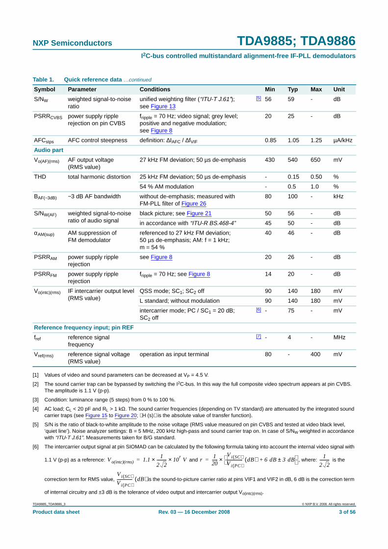
Table 1. Quick reference data
Symbol Parameter Conditions Min Typ Max Unit
VP supply voltage [1] 4.5 5.0 5.5 V
IP supply current 52 63 70 mA
τP time constant (R × C) fornetwork at pin VP
for applications without I2C-bus 1.2 - - µs
Video part
Vi(VIF)(rms) VIF input voltagesensitivity (RMS value)
−1 dB video at output - 60 100 µV
GVIF(cr) control range VIF gain see Figure 9 60 66 - dB
fVIF vision carrier operatingfrequencies
see Table 13 - 33.4 - MHz
- 33.9 - MHz
- 38.0 - MHz
- 38.9 - MHz
- 45.75 - MHz
- 58.75 - MHz
∆fVIF VIF frequency window ofdigital acquisition help
related to fVIF; see Figure 12 - ±2.3 - MHz
Vo(v)(p-p) video output voltage(peak-to-peak value)
see Figure 7
normal mode (sound carrier trap active)and sound carrier on
1.7 2.0 2.3 V
trap bypass mode and sound carrier off [2] 0.95 1.10 1.25 V
Gdif differential gain “ITU-T J.63 line 330” [3]
B/G standard - - 5 %
L standard - - 7 %
ϕdif differential phase “ITU-T J.63 line 330” - 2 4 deg
Bv(−1dB) −1 dB video bandwidth trap bypass mode and sound carrier off;AC load: CL < 20 pF, RL > 1 kΩ
[2] 5 6 - MHz
Bv(−3dB)(trap) −3 dB video bandwidthincluding sound carriertrap
ftrap = 4.5 MHz [4] 3.95 4.05 - MHz
ftrap = 5.5 MHz [4] 4.90 5.00 - MHz
ftrap = 6.0 MHz [4] 5.40 5.50 - MHz
ftrap = 6.5 MHz [4] 5.50 5.95 - MHz
αSC1 attenuation at first soundcarrier
f = 4.5 MHz 30 36 - dB
f = 5.5 MHz 30 36 - dB
TDA9885_TDA9886_3 © NXP B.V. 2008. All rights reserved.
Product data sheet Rev. 03 — 16 December 2008 2 of 56
NXP Semiconductors TDA9885; TDA9886I2C-bus controlled multistandard alignment-free IF-PLL demodulators
[1] Values of video and sound parameters can be decreased at VP = 4.5 V.
[2] The sound carrier trap can be bypassed by switching the I2C-bus. In this way the full composite video spectrum appears at pin CVBS.The amplitude is 1.1 V (p-p).
[3] Condition: luminance range (5 steps) from 0 % to 100 %.
[4] AC load; CL < 20 pF and RL > 1 kΩ. The sound carrier frequencies (depending on TV standard) are attenuated by the integrated soundcarrier traps (see Figure 15 to Figure 20; H (s) is the absolute value of transfer function).
[5] S/N is the ratio of black-to-white amplitude to the noise voltage (RMS value measured on pin CVBS and tested at video black level,‘quiet line’). Noise analyzer settings: B = 5 MHz, 200 kHz high-pass and sound carrier trap on. In case of S/NW weighted in accordancewith “ITU-T J.61”. Measurements taken for B/G standard.
[6] The intercarrier output signal at pin SIOMAD can be calculated by the following formula taking into account the internal video signal with
1.1 V (p-p) as a reference: and , where: is the
correction term for RMS value, is the sound-to-picture carrier ratio at pins VIF1 and VIF2 in dB, 6 dB is the correction term
of internal circuitry and ±3 dB is the tolerance of video output and intercarrier output Vo(intc)(rms).
S/NW weighted signal-to-noiseratio
unified weighting filter (“ITU-T J.61”);see Figure 13
[5] 56 59 - dB
PSRRCVBS power supply ripplerejection on pin CVBS
fripple = 70 Hz; video signal; grey level;positive and negative modulation;see Figure 8
20 25 - dB
AFCstps AFC control steepness definition: ∆IAFC / ∆fVIF 0.85 1.05 1.25 µA/kHz
Audio part
Vo(AF)(rms) AF output voltage(RMS value)
27 kHz FM deviation; 50 µs de-emphasis 430 540 650 mV
THD total harmonic distortion 25 kHz FM deviation; 50 µs de-emphasis - 0.15 0.50 %
54 % AM modulation - 0.5 1.0 %
BAF(−3dB) −3 dB AF bandwidth without de-emphasis; measured withFM-PLL filter of Figure 26
80 100 - kHz
S/NW(AF) weighted signal-to-noiseratio of audio signal
black picture; see Figure 21 50 56 - dB
in accordance with “ITU-R BS.468-4” 45 50 - dB
αAM(sup) AM suppression ofFM demodulator
referenced to 27 kHz FM deviation;50 µs de-emphasis; AM: f = 1 kHz;m = 54 %
40 46 - dB
PSRRAM power supply ripplerejection
see Figure 8 20 26 - dB
PSRRFM power supply ripplerejection
fripple = 70 Hz; see Figure 8 14 20 - dB
Vo(intc)(rms) IF intercarrier output level(RMS value)
QSS mode; SC1; SC2 off 90 140 180 mV
L standard; without modulation 90 140 180 mV
intercarrier mode; PC / SC1 = 20 dB;SC2 off
[6] - 75 - mV
Reference frequency input; pin REF
fref reference signalfrequency
[7] - 4 - MHz
Vref(rms) reference signal voltage(RMS value)
operation as input terminal 80 - 400 mV
Table 1. Quick reference data …continued
Symbol Parameter Conditions Min Typ Max Unit
Vo(intc)(rms) 1.11
2 2----------× 10
r× V= r120------
Vi SC( )Vi PC( )---------------- dB( ) 6 dB 3 dB±+
×=1
2 2----------
Vi SC( )Vi PC( )---------------- dB( )
TDA9885_TDA9886_3 © NXP B.V. 2008. All rights reserved.
Product data sheet Rev. 03 — 16 December 2008 3 of 56
NXP Semiconductors TDA9885; TDA9886I2C-bus controlled multistandard alignment-free IF-PLL demodulators
[7] Pin REF is able to operate as a 1-pin crystal oscillator input as well as an external reference signal input, e.g. from the tuning system.
5. Ordering information
Table 2. Ordering information
Type number Package
Name Description Version
TDA9885T/V3 SO24 plastic small outline package; 24 leads; body width 7.5 mm SOT137-1
TDA9885TS/V3 SSOP24 plastic shrink small outline package; 24 leads; body width 5.3 mm SOT340-1
TDA9885HN/V3 HVQFN32 plastic thermal enhanced very thin quad flat package; no leads;32 terminals; body 5 × 5 × 0.85 mm
SOT617-3
TDA9886T/V4 SO24 plastic small outline package; 24 leads; body width 7.5 mm SOT137-1
TDA9886TS/V4 SSOP24 plastic shrink small outline package; 24 leads; body width 5.3 mm SOT340-1
TDA9886HN/V4 HVQFN32 plastic thermal enhanced very thin quad flat package; no leads;32 terminals; body 5 × 5 × 0.85 mm
SOT617-3
TDA9885T/V5 SO24 plastic small outline package; 24 leads; body width 7.5 mm SOT137-1
TDA9885TS/V5 SSOP24 plastic shrink small outline package; 24 leads; body width 5.3 mm SOT340-1
TDA9885HN/V5 HVQFN32 plastic thermal enhanced very thin quad flat package; no leads;32 terminals; body 5 × 5 × 0.85 mm
SOT617-3
TDA9886T/V5 SO24 plastic small outline package; 24 leads; body width 7.5 mm SOT137-1
TDA9886TS/V5 SSOP24 plastic shrink small outline package; 24 leads; body width 5.3 mm SOT340-1
TDA9886HN/V5 HVQFN32 plastic thermal enhanced very thin quad flat package; no leads;32 terminals; body 5 × 5 × 0.85 mm
SOT617-3
TDA9885_TDA9886_3 © NXP B.V. 2008. All rights reserved.
Product data sheet Rev. 03 — 16 December 2008 4 of 56
xxxx xxxxxxxxxxxxxxxxxxxxxxxxxxxxxx x xxxxxxxxxxxxxx xxxxxxxxxx xxx xxxxxx xxxxxxxxxxxxxxxxxxxxxxx xxxxxxxxxxxxxxxxxxxxxxxxxxx xxxxxx xx xxxxxxxxxxxxxxxxxxxxxxxxxxxxx xxxxxxxxxxxxxxxxxxxxxx xxxxxxxxxxx xxxxxxx xxxxxxxxxxxxxxxxxxxxxxxxxxxxxxxxxxx xxxxxxxxxxxxxx xxxxxx xx xxxxxxxxxxxxxxxxxxxxxxxxxxxxxxxx xxxxxxxxxxxxxxxxxxxxxxxx xxxxxxxxxxxxxxxxxxxxxxxxxxxxxxxxxxxxxxxxxxxxxxxxxxxxx xxxxxxxxxxx xxxxx x x
TD
A9885_T
DA
9886_3
Product data shee
NX
P S
emiconducto
6.B
lock diagram
CVAGC(pos)
external reference signalor 4 MHz crystalVIF-PLL
t
TAGC VAGC(1)TOP
14 (15)
VPLL
19 (21)9 (8) 16 (17) 15 (16) 21 (23)
REF AFC
filter
rsT
DA
9885; TD
A9886
I 2C-bus controlled m
ultistandard alignment-free IF
-PLL dem
odulators
008aaa174
G
(18) 17
(7) 8
(3) 5
(4) 6
AUD
CVBS
audio output
video output: 2 V (p-p)[1.1 V (p-p) without trap]
CAF
DEEM
AFD
LLr
de-emphasisnetwork
© N
XP
B.V. 2008. A
ll rights reserved.
Rev. 03 —
16 Decem
ber 20085 of 56
Pin numbers for TDA9885HN and TDA9886HN in parentheses.
(1) Not connected for TDA9885
Fig 1. Block diagram of TDA9885; TDA9886
DIGITAL VCO CONTROL AFC DETECTORRC VCO
VIF PLL
VIF AGCTUNER AGC
SUPPLY SIF AGC
AUDIO PROCESSINAND SWITCHES
NARROWBANDFM-PLL DEMODULATOR
SINGLE REFERENCE QSS MIXERINTERCARRIER MIXER
AND AM DEMODULATOR
SOUND CARRIERTRAPS
4.5 MHz to 6.5 MHz
CAGC(neg) CBL
4 (2)10 (9)11 (10) 12 (11)18 (20)20 (22)
2 (31)
1 (30)
SIOMADSDASCL
MAD
VP
CAGC
(6, 12, 13, 14, 17,19, 25, 28, 29, 32)13
n.c.AGND
7 (5)
DGND
OUTPUTPORTS
I2C-BUS TRANSCEIVER
22 (24)3 (1)
OP1 OP2 FMPLL
sound intercarrier outputand MAD select
FM-Pfilte
VIF2
VIF1
24 (27)
23 (26)
SIF2
SIF1
TDA9885TDA9886
NXP Semiconductors TDA9885; TDA9886I2C-bus controlled multistandard alignment-free IF-PLL demodulators
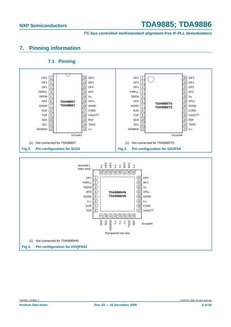
7. Pinning information
7.1 Pinning
(1) Not connected for TDA9885T (1) Not connected for TDA9885TS
Fig 2. Pin configuration for SO24 Fig 3. Pin configuration for SSOP24
TDA9885TTDA9886T
VIF1 SIF2
VIF2 SIF1
OP1 OP2
FMPLL AFC
DEEM VP
AFD VPLL
DGND AGND
AUD CVBS
TOP VAGC(1)
SDA REF
SCL TAGC
SIOMAD n.c.
001aai897
1
2
3
4
5
6
7
8
9
10
11
12
14
13
16
15
18
17
20
19
22
21
24
23
TDA9885TSTDA9886TS
VIF1 SIF2
VIF2 SIF1
OP1 OP2
FMPLL AFC
DEEM VP
AFD VPLL
DGND AGND
AUD CVBS
TOP VAGC(1)
SDA REF
SCL TAGC
SIOMAD n.c.
001aai898
1
2
3
4
5
6
7
8
9
10
11
12
14
13
16
15
18
17
20
19
22
21
24
23
(1) Not connected for TDA9885HN
Fig 4. Pin configuration for HVQFN32
001aai899
TDA9885HNTDA9886HN
Transparent top view
VAGC(1)
AUD
TOP
CVBS
n.c. n.c.
DGND AGND
AFD VPLL
DEEM VP
FMPLL AFC
OP1 OP2
SD
A
SC
L
SIO
MA
D
n.c.
n.c.
n.c.
TA
GC
RE
F
n.c.
VIF
2
VIF
1
n.c.
n.c.
SIF
2
SIF
1
n.c.
8 17
7 18
6 19
5 20
4 21
3 22
2 23
1 24
9 10 11 12 13 14 15 16
32 31 30 29 28 27 26 25
terminal 1index area
TDA9885_TDA9886_3 © NXP B.V. 2008. All rights reserved.
Product data sheet Rev. 03 — 16 December 2008 6 of 56

NXP Semiconductors TDA9885; TDA9886I2C-bus controlled multistandard alignment-free IF-PLL demodulators
7.2 Pin description
Table 3. Pin description
Symbol Pin Description
TDA9885TTDA9885TS
TDA9886TTDA9886TS
TDA9885HN TDA9886HN
VIF1 1 1 30 30 VIF differential input 1
VIF2 2 2 31 31 VIF differential input 2
n.c. - - 32 32 not connected
OP1 3 3 1 1 output port 1; open-collector
FMPLL 4 4 2 2 FM PLL for loop filter
DEEM 5 5 3 3 de-emphasis output for capacitor
AFD 6 6 4 4 AF DC-decoupling capacitor
DGND 7 7 5 5 digital ground
n.c. - - 6 6 not connected
AUD 8 8 7 7 audio output
TOP 9 9 8 8 tuner AGC TOP for resistor adjustment
SDA 10 10 9 9 I2C-bus data input and output
SCL 11 11 10 10 I2C-bus clock input
SIOMAD 12 12 11 11 sound intercarrier output and MAD select with resistor
n.c. - - 12 12 not connected
n.c. 13 13 13 13 not connected
n.c. - - 14 14 not connected
TAGC 14 14 15 15 tuner AGC output
REF 15 15 16 16 4 MHz crystal or reference signal input
VAGC - 16 - 17 VIF AGC for capacitor
n.c. 16 - 17 - not connected
CVBS 17 17 18 18 composite video output
n.c. - - 19 19 not connected
AGND 18 18 20 20 analog ground
VPLL 19 19 21 21 VIF PLL for loop filter
VP 20 20 22 22 supply voltage
AFC 21 21 23 23 AFC output
OP2 22 22 24 24 output port 2; open-collector
n.c. - - 25 25 not connected
SIF1 23 23 26 26 SIF differential input 1 and MAD select with resistor
SIF2 24 24 27 27 SIF differential input 2 and MAD select with resistor
n.c. - - 28 28 not connected
n.c. - - 29 29 not connected
TDA9885_TDA9886_3 © NXP B.V. 2008. All rights reserved.
Product data sheet Rev. 03 — 16 December 2008 7 of 56
NXP Semiconductors TDA9885; TDA9886I2C-bus controlled multistandard alignment-free IF-PLL demodulators
8. Functional description
Figure 1 shows the simplified block diagram of the device which comprises the followingfunctional blocks:
• VIF amplifier
• Tuner AGC and VIF AGC
• VIF-AGC detector
• Frequency Phase-Locked Loop (FPLL) detector
• VCO and divider
• AFC and digital acquisition help
• Video demodulator and amplifier
• Sound carrier trap
• SIF amplifier
• SIF-AGC detector
• Single reference QSS mixer
• AM demodulator
• FM demodulator and acquisition help
• Audio amplifier and mute time constant
• Internal voltage stabilizer
• I2C-bus transceiver and MAD
8.1 VIF amplifierThe VIF amplifier consists of three AC-coupled differential stages. Gain control isperformed by emitter degeneration and collector resistor variation. The total gain controlrange is typically 66 dB. The differential input impedance is typically 2 kΩ in parallel with3 pF.
8.2 Tuner AGC and VIF AGCThis block adapts the voltage, generated at the VIF-AGC detector, to the internal signalprocessing at the VIF amplifier and performs the tuner AGC control current generation.The onset of the tuner AGC control current generation can be set either via the I2C-bus(see Table 12) or optionally by a potentiometer at pin TOP (in case that the I2C-businformation cannot be stored, related to the device). The presence of a potentiometer isautomatically detected and the I2C-bus setting is disabled.
Furthermore, derived from the AGC detector voltage, a comparator is used to detect if thecorresponding VIF input voltage is higher than 200 µV. This information can be read outvia the I2C-bus (bit VIFLEV = 1).
TDA9885_TDA9886_3 © NXP B.V. 2008. All rights reserved.
Product data sheet Rev. 03 — 16 December 2008 8 of 56

NXP Semiconductors TDA9885; TDA9886I2C-bus controlled multistandard alignment-free IF-PLL demodulators
8.3 VIF-AGC detectorGain control is performed by sync level detection (negative modulation) or peak whitedetection (positive modulation).
For negative modulation, the sync level voltage is stored at an integrated capacitor bymeans of a fast peak detector. This voltage is compared with a reference voltage (nominalsync level) by a comparator which charges or discharges the integrated AGC capacitor forproviding of the required VIF gain. The time constants for decreasing or increasing thegain are nearly equal and the total AGC reaction time is fast to cope with ‘aeroplanefluttering’.
For positive modulation, the white peak level voltage is compared with a reference voltage(nominal white level) by a comparator which charges (fast) or discharges (slow) theexternal AGC capacitor directly for providing the required VIF gain. The need of a verylong time constant for VIF gain increase is due to peak white level may appear only oncein a field. In order to reduce this time constant, an additional level detector increases thedischarging current of the AGC capacitor (fast mode) in the event of a decreasing VIFamplitude step controlled by the detected actual black level voltage. The threshold level forfast mode AGC is typically −6 dB video amplitude. The fast mode state is also transferredto the SIF-AGC detector for speed-up. In case of missing peak white pulses, the VIF gainincrease is limited to typically +3 dB by comparing the detected actual black level voltagewith a corresponding reference voltage.
8.4 FPLL detectorThe VIF amplifier output signal is fed into a frequency detector and into a phase detectorvia a limiting amplifier for removing the video AM.
During acquisition the frequency detector produces a current proportional to thefrequency difference between the VIF and the VCO signals. After frequency lock-in thephase detector produces a current proportional to the phase difference between the VIFand the VCO signals. The currents from the frequency and phase detectors are chargedinto the loop filter which controls the VIF VCO and locks it to the frequency and phase ofthe VIF carrier.
For a positive modulated VIF signal, the charging currents are optional gated by thecomposite sync in order to avoid signal distortion in case of overmodulation. The gatingdepth is switchable via the I2C-bus.
8.5 VCO and dividerThe VCO of the VIF FPLL operates as an integrated low radiation relaxation oscillator atdouble the picture carrier frequency. The control voltage, required to tune the VCO todouble the picture carrier frequency, is generated at the loop filter by the frequency phasedetector. The possible frequency range is 50 MHz to 140 MHz (typical value).
The oscillator frequency is divided-by-two to provide two differential square wave signalswith exactly 90 degrees phase difference, independent of the frequency, for use in theFPLL detectors, the video demodulator and the intercarrier mixer.
TDA9885_TDA9886_3 © NXP B.V. 2008. All rights reserved.
Product data sheet Rev. 03 — 16 December 2008 9 of 56

NXP Semiconductors TDA9885; TDA9886I2C-bus controlled multistandard alignment-free IF-PLL demodulators
8.6 AFC and digital acquisition helpEach relaxation oscillator of the VIF-PLL and FM-PLL demodulator has a wide frequencyrange. To prevent false locking of the PLLs and with respect to the catching range, thedigital acquisition help provides an individual control, until the frequency of the VCO iswithin the preselected standard dependent lock-in window of the PLL.
The in-window and out-window control at the FM PLL is additionally used to mute theaudio stage (if auto mute is selected via the I2C-bus).
The working principle of the digital acquisition help is as follows. The PLL VCO output isconnected to a down counter which has a predefined start value (standard dependent).The VCO frequency clocks the down counter for a fixed gate time. Thereafter, the downcounter stop value is analyzed. In case the stop value is higher (lower) than the expectedvalue range, the VCO frequency is lower (higher) than the wanted lock-in windowfrequency range. A positive (negative) control current is injected into the PLL loop filterand consequently the VCO frequency is increased (decreased) and a new counting cyclestarts.
The gate time as well as the control logic of the acquisition help circuit is dependent on theprecision of the reference signal at pin REF. Operation as a crystal oscillator is possible aswell as connecting this input via a serial capacitor to an external reference frequency, e.g.the tuning system oscillator.
The AFC signal is derived from the corresponding down counter stop value after acounting cycle. The last four bits are latched and can be read out via the I2C-bus(see Table 8). Also the digital-to-analog converted value is given as current at pin AFC.
8.7 Video demodulator and amplifierThe video demodulator is realized by a multiplier which is designed for low distortion andlarge bandwidth. The VIF signal is multiplied with the ‘in phase’ signal of the VIF-PLLVCO.
The demodulator output signal is fed into the video preamplifier via a level shift stage withintegrated low-pass filter to achieve carrier harmonics attenuation.
The output signal of the preamplifier is fed to the VIF-AGC detector (see Section 8.3) andin the sound trap mode also fed internally to the integrated sound carrier trap(see Section 8.8). The differential trap output signal is converted to a single-ended signaland amplified by the following post-amplifier. The video output level at pin CVBS is2 V (p-p).
In the trap bypass mode the output signal of the preamplifier is fed directly through thepost-amplifier to pin CVBS. The output video level is 1.1 V (p-p) for using an externalsound trap with 10 % overall loss.
Noise clipping is provided in both cases.
TDA9885_TDA9886_3 © NXP B.V. 2008. All rights reserved.
Product data sheet Rev. 03 — 16 December 2008 10 of 56
NXP Semiconductors TDA9885; TDA9886I2C-bus controlled multistandard alignment-free IF-PLL demodulators
8.8 Sound carrier trapThe sound trap is constructed of three separate traps to realize sufficient suppression ofthe first and second sound carriers.
For frequency control of the sound trap additionally a reference low-pass filter and aphase detector are built in.
A sound carrier reference signal is fed into the reference low-pass filter and is shifted bynominal 90 degrees. The phase detector compares the original reference signal with thesignal shifted by the reference filter and produces a DC voltage by charging or dischargingan integrated capacitor with a current proportional to the phase difference between bothsignals, respectively to the frequency error of the integrated filters. The DC voltagecontrols the frequency position of the reference filter and the sound trap. So the accuratefrequency position for the different standards is set by the sound carrier reference signal.
8.9 SIF amplifierThe SIF amplifier consists of three AC-coupled differential stages. Gain control isperformed by emitter degeneration and collector resistor variation. The total gain controlrange is typically 66 dB. The differential input impedance is typically 2 kΩ in parallel with3 pF.
8.10 SIF-AGC detectorSIF gain control is performed by detection and controlling to a reference value of theDC component of the AM demodulator output signal. This DC signal corresponds directlyto the SIF voltage at the output of the SIF amplifier so that a constant SIF signal issupplied to the AM demodulator and to the single reference QSS mixer.
By switching the gain of the input amplifier of the SIF-AGC detector via the I2C-bus, theinternal SIF level for FM sound is 5.5 dB lower than for AM sound. This is to adapt theSIF-AGC characteristic to the VIF-AGC characteristic. The adaption is ideal for apicture-to-sound FM carrier ratio of 13 dB.
Via a comparator, the integrated AGC capacitor is charged or discharged for providing therequired SIF gain. Due to AM sound, the AGC reaction time is slow (fc < 20 Hz for theclosed AGC loop). For reducing this AM sound time constant in the event of a decreasingIF amplitude step, the charge/discharge current of the AGC capacitor is increased (fastmode) when the VIF-AGC detector (at positive modulation mode) operates in the fastmode too. An additional circuit (threshold approximately 7 dB) ensures a very fast gainreduction for a large increasing IF amplitude step.
8.11 Single reference QSS mixerWith the present system a high performance Hi-Fi stereo sound processing can beachieved. For a simplified application without a SIF SAW filter, the single reference QSSmixer can be switched to the intercarrier mode via the I2C-bus.
The single reference QSS mixer generates the 2nd FM TV sound intercarrier signal. It isrealized by a linear multiplier which multiplies the SIF amplifier output signal and theVIF-PLL VCO signal (90 degrees output) which is locked to the picture carrier. In this waythe QSS mixer operates as a quadrature mixer in the intercarrier mode and providessuppression of the low frequency video signals.
TDA9885_TDA9886_3 © NXP B.V. 2008. All rights reserved.
Product data sheet Rev. 03 — 16 December 2008 11 of 56

NXP Semiconductors TDA9885; TDA9886I2C-bus controlled multistandard alignment-free IF-PLL demodulators
The QSS mixer output signal is fed internally via a high-pass and low-pass combination tothe FM demodulator as well as via an operational amplifier to the intercarrier outputpin SIOMAD.
8.12 AM demodulatorThe amplitude modulated SIF amplifier output signal is fed both to a two-stage limitingamplifier that removes the AM and to a linear multiplier. The result of the multiplication ofthe SIF signal with the limiter output signal is AM demodulation (passive synchronousdemodulator). The demodulator output signal is fed via a low-pass filter that attenuatesthe carrier harmonics and through the input amplifier of the SIF-AGC detector to the audioamplifier.
8.13 FM demodulator and acquisition helpThe narrowband FM-PLL detector consists of:
• Gain controlled FM amplifier and AGC detector
• Narrowband PLL
The 2nd SIF signal from the intercarrier mixer is fed to the input of an AC-coupled gaincontrolled amplifier with two stages. The gain controlled output signal is fed to the phasedetector of the narrowband FM PLL (FM demodulator). For good selectivity androbustness against disturbance caused by the video signal, a high linearity of the gaincontrolled FM amplifier and of the phase detector as well as a constant signal level arerequired. The gain control is done by means of an ‘in phase’ demodulator for the 2nd SIFsignal (from the output of the FM amplifier). The demodulation output is fed into acomparator for charging or discharging the integrated AGC capacitor. This leads to amean value AGC loop to control the gain of the FM amplifier.
The FM demodulator is realized as a narrowband PLL with an external loop filter, whichprovides the necessary selectivity (bandwidth approximately 100 kHz). To achieve goodselectivity, a linear phase detector and a constant input level are required. The gaincontrolled intercarrier signal from the FM amplifier is fed to the phase detector. The phasedetector controls via the loop filter the integrated low radiation relaxation oscillator. Thedesigned frequency range is from 4 MHz to 7 MHz.
The VCO within the FM PLL is phase-locked to the incoming 2nd SIF signal, which isfrequency modulated. As well as this, the VCO control voltage is superimposed by theAF voltage. Therefore, the VCO tracks with the FM of the 2nd SIF signal. So, theAF voltage is present at the loop filter and is typically 5 mV (RMS) for 27 kHzFM deviation. This AF signal is fed via a buffer to the audio amplifier.
The correct locking of the PLL is supported by the digital acquisition help circuit(see Section 8.6).
8.14 Audio amplifier and mute time constantThe audio amplifier consists of two parts:
• AF preamplifier
• AF output amplifier
TDA9885_TDA9886_3 © NXP B.V. 2008. All rights reserved.
Product data sheet Rev. 03 — 16 December 2008 12 of 56
NXP Semiconductors TDA9885; TDA9886I2C-bus controlled multistandard alignment-free IF-PLL demodulators
The AF preamplifier used for FM sound is an operational amplifier with internal feedback,high gain and high common mode rejection. The AF voltage from the PLL demodulator is5 mV (RMS) for a frequency deviation of 27 kHz and is amplified by 30 dB. By the use of aDC operating point control circuit (with external capacitor CAF), the AF preamplifier isdecoupled from the PLL DC voltage. The low-pass characteristic of the amplifier reducesthe harmonics of the 2nd SIF signal at the AF output terminal.
For FM sound a switchable de-emphasis network (with external capacitor) is implementedbetween the preamplifier and the output amplifier.
The AF output amplifier provides the required AF output level by a rail-to-rail output stage.A preceding stage makes use of an input selector for switching between FM sound,AM sound and mute state. The gain can be switched between 10 dB (normal) and 4 dB(reduced).
Switching to the mute state is controlled automatically, dependent on the digitalacquisition help in case the VCO of the FM PLL is not in the required frequency window.This is done by a time constant: fast for switching to the mute state and slow (typically40 ms) for switching to the no-mute state.
All switching functions are controlled via the I2C-bus:
• AM sound, FM sound and forced mute
• Auto mute enable or disable
• De-emphasis off or on with 50 µs or 75 µs
• Audio gain normal or reduced
8.15 Internal voltage stabilizerThe band gap circuit internally generates a voltage of approximately 2.4 V, independent ofsupply voltage and temperature. A voltage regulator circuit, connected to this voltage,produces a constant voltage of 3.55 V which is used as an internal reference voltage.
8.16 I2C-bus transceiver and MADThe device can be controlled via the 2-wire I2C-bus by a microcontroller. Two wires carryserial data (SDA) and serial clock (SCL) information between the devices connected tothe I2C-bus.
The device has an I2C-bus slave transceiver with auto-increment. The circuit operates upto clock frequencies of 400 kHz.
A slave address is sent from the master to the slave receiver. To avoid conflicts in a realapplication with other devices providing similar or complementing functions, there are fourpossible slave addresses available. These MADs can be selected by connecting resistorson pin SIOMAD and/or pins SIF1 and SIF2 (see Figure 26). Pin SIOMAD relates withbit A0 and pins SIF1 and SIF2 relate with bit A3. The slave addresses of this device aregiven in Table 4.
The power-on preset value is dependent on the use of pin SIOMAD and can be chosen for45.75 MHz NTSC as default (pin SIOMAD left open-circuit) or 58.75 MHz NTSC (resistoron pin SIOMAD). In this way the device can be used without the I2C-bus as an NTSC onlydevice.
TDA9885_TDA9886_3 © NXP B.V. 2008. All rights reserved.
Product data sheet Rev. 03 — 16 December 2008 13 of 56
NXP Semiconductors TDA9885; TDA9886I2C-bus controlled multistandard alignment-free IF-PLL demodulators
Remark: In case of using the device without the I2C-bus, then the rise time of the supplyvoltage after switching on power must be longer than 1.2 µs.
9. I2C-bus control
9.1 Read format
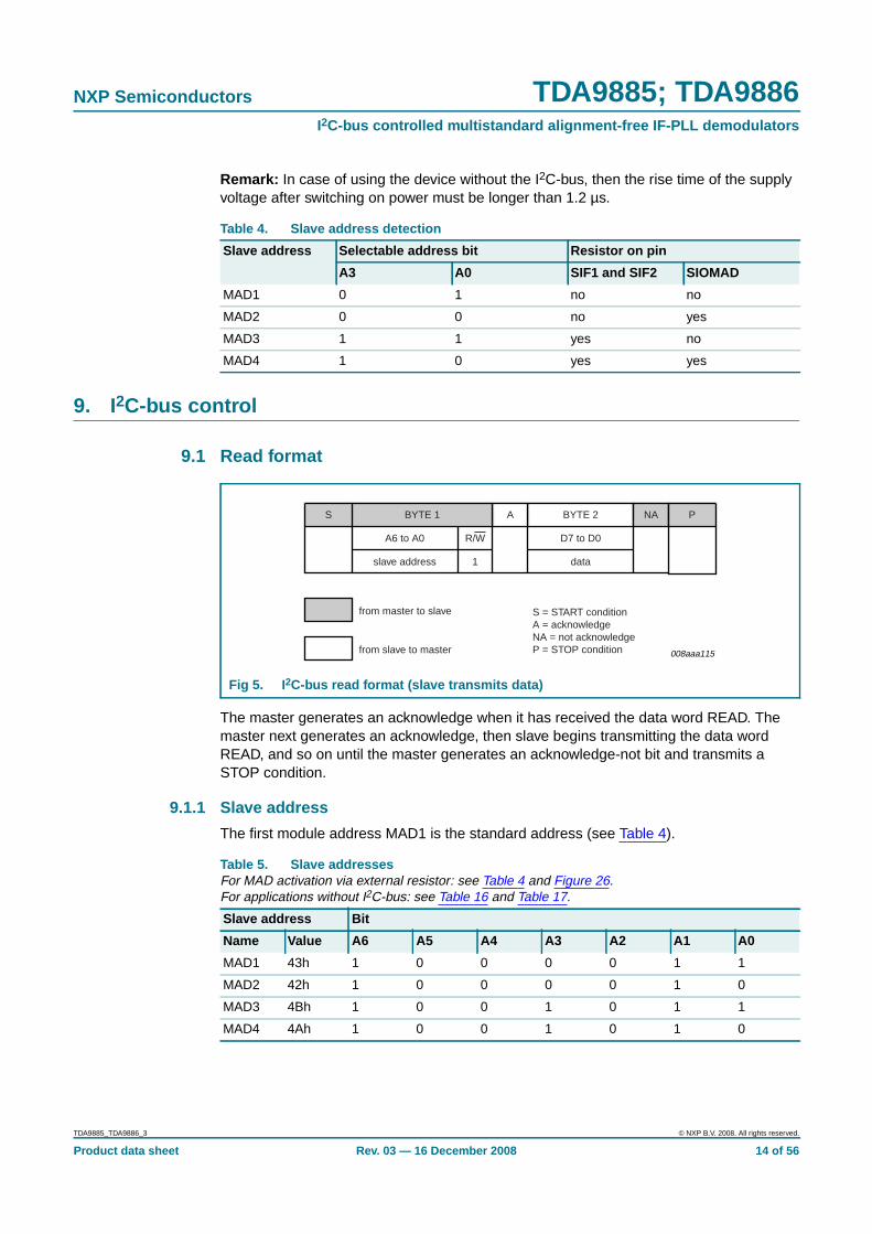
The master generates an acknowledge when it has received the data word READ. Themaster next generates an acknowledge, then slave begins transmitting the data wordREAD, and so on until the master generates an acknowledge-not bit and transmits aSTOP condition.
9.1.1 Slave address
The first module address MAD1 is the standard address (see Table 4).
Table 4. Slave address detection
Slave address Selectable address bit Resistor on pin
A3 A0 SIF1 and SIF2 SIOMAD
MAD1 0 1 no no
MAD2 0 0 no yes
MAD3 1 1 yes no
MAD4 1 0 yes yes
Fig 5. I2C-bus read format (slave transmits data)
008aaa115
A6 to A0 R/W D7 to D0
slave address 1 data
S BYTE 1 A BYTE 2 NA P
from master to slave S = START conditionA = acknowledgeNA = not acknowledgeP = STOP conditionfrom slave to master
Table 5. Slave addressesFor MAD activation via external resistor: see Table 4 and Figure 26.For applications without I2C-bus: see Table 16 and Table 17.
Slave address Bit
Name Value A6 A5 A4 A3 A2 A1 A0
MAD1 43h 1 0 0 0 0 1 1
MAD2 42h 1 0 0 0 0 1 0
MAD3 4Bh 1 0 0 1 0 1 1
MAD4 4Ah 1 0 0 1 0 1 0
TDA9885_TDA9886_3 © NXP B.V. 2008. All rights reserved.
Product data sheet Rev. 03 — 16 December 2008 14 of 56
NXP Semiconductors TDA9885; TDA9886I2C-bus controlled multistandard alignment-free IF-PLL demodulators
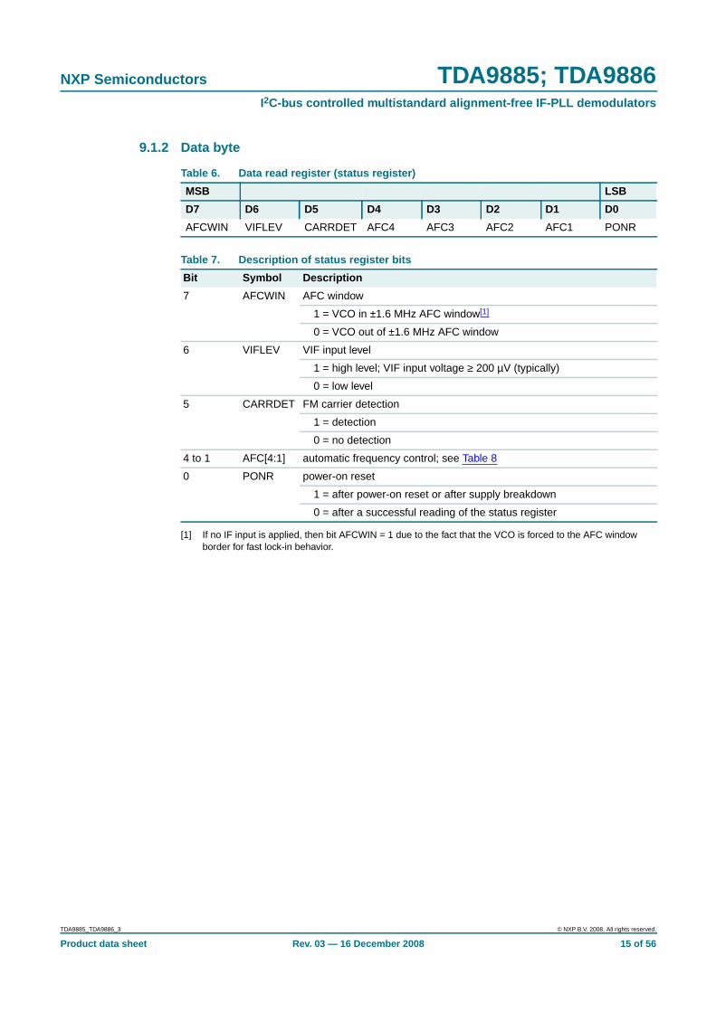
9.1.2 Data byte
[1] If no IF input is applied, then bit AFCWIN = 1 due to the fact that the VCO is forced to the AFC windowborder for fast lock-in behavior.
Table 6. Data read register (status register)
MSB LSB
D7 D6 D5 D4 D3 D2 D1 D0
AFCWIN VIFLEV CARRDET AFC4 AFC3 AFC2 AFC1 PONR
Table 7. Description of status register bits
Bit Symbol Description
7 AFCWIN AFC window
1 = VCO in ±1.6 MHz AFC window[1]
0 = VCO out of ±1.6 MHz AFC window
6 VIFLEV VIF input level
1 = high level; VIF input voltage ≥ 200 µV (typically)
0 = low level
5 CARRDET FM carrier detection
1 = detection
0 = no detection
4 to 1 AFC[4:1] automatic frequency control; see Table 8
0 PONR power-on reset
1 = after power-on reset or after supply breakdown
0 = after a successful reading of the status register
TDA9885_TDA9886_3 © NXP B.V. 2008. All rights reserved.
Product data sheet Rev. 03 — 16 December 2008 15 of 56
NXP Semiconductors TDA9885; TDA9886I2C-bus controlled multistandard alignment-free IF-PLL demodulators
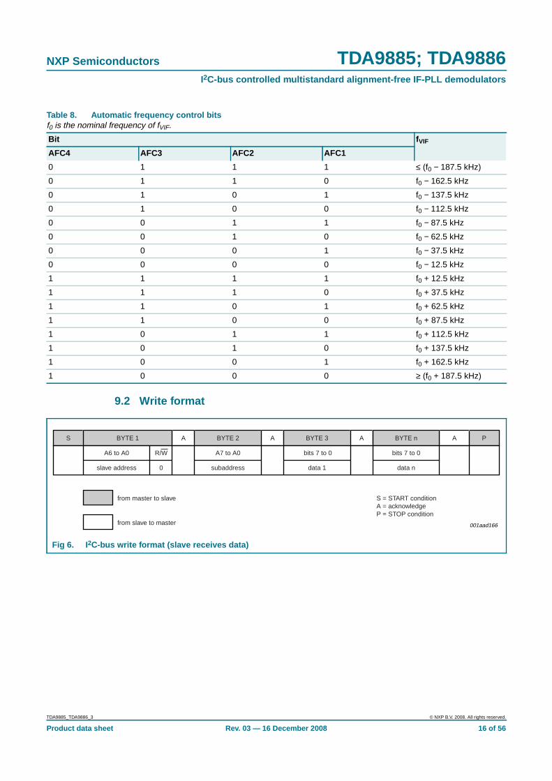
9.2 Write format
Table 8. Automatic frequency control bitsf0 is the nominal frequency of fVIF.
Bit fVIF
AFC4 AFC3 AFC2 AFC1
0 1 1 1 ≤ (f0 − 187.5 kHz)
0 1 1 0 f0 − 162.5 kHz
0 1 0 1 f0 − 137.5 kHz
0 1 0 0 f0 − 112.5 kHz
0 0 1 1 f0 − 87.5 kHz
0 0 1 0 f0 − 62.5 kHz
0 0 0 1 f0 − 37.5 kHz
0 0 0 0 f0 − 12.5 kHz
1 1 1 1 f0 + 12.5 kHz
1 1 1 0 f0 + 37.5 kHz
1 1 0 1 f0 + 62.5 kHz
1 1 0 0 f0 + 87.5 kHz
1 0 1 1 f0 + 112.5 kHz
1 0 1 0 f0 + 137.5 kHz
1 0 0 1 f0 + 162.5 kHz
1 0 0 0 ≥ (f0 + 187.5 kHz)
Fig 6. I2C-bus write format (slave receives data)
001aad166
A6 to A0 R/W A7 to A0 bits 7 to 0
slave address
from master to slave S = START conditionA = acknowledgeP = STOP condition
0 subaddress data 1 data n
bits 7 to 0
from slave to master
S BYTE 1 A BYTE 2 A ABYTE 3 BYTE n A P
TDA9885_TDA9886_3 © NXP B.V. 2008. All rights reserved.
Product data sheet Rev. 03 — 16 December 2008 16 of 56

NXP Semiconductors TDA9885; TDA9886I2C-bus controlled multistandard alignment-free IF-PLL demodulators
9.2.1 Subaddress (A data)
If more than one data byte is transmitted, then auto-increment is performed: starting fromthe transmitted subaddress and auto-increment of subaddress in accordance with theorder of Table 9.
[1] Bit A7 = 1 is not allowed.
[2] Bits A6 to A2 will be ignored by the internal hardware.
9.2.2 Data byte for switching mode (B data)
[1] For positive AM TV choose 6.5 MHz for the second SIF.
Table 9. Definition of the subaddress (second byte after slave address)X = don’t care.
Register MSB LSB
A7[1] A6[2] A5[2] A4[2] A3[2] A2[2] A1 A0
SAD for switching mode 0 X X X X X 0 0
SAD for adjust mode 0 X X X X X 0 1
SAD for data mode 0 X X X X X 1 0
Table 10. Bit description of SAD register for switching mode (SAD = 00)
Bit Symbol Description
7 B7 output port 2 for SAW switching or monitoring
1 = high-impedance, disabled or HIGH
0 = low-impedance, active or LOW
6 B6 output port 1 for SAW switching or external input
1 = high-impedance, disabled or HIGH
0 = low-impedance, active or LOW
5 B5 forced audio mute
1 = on
0 = off
4 and 3 B[4:3] TV standard modulation
00 = positive AM TV[1]
01 = not used
10 = negative FM TV
11 = not used
2 B2 carrier mode
1 = QSS mode
0 = intercarrier mode
1 B1 auto mute of FM AF output
1 = active
0 = inactive
0 B0 video mode (sound trap)
1 = sound trap bypass
0 = sound trap active
TDA9885_TDA9886_3 © NXP B.V. 2008. All rights reserved.
Product data sheet Rev. 03 — 16 December 2008 17 of 56
NXP Semiconductors TDA9885; TDA9886I2C-bus controlled multistandard alignment-free IF-PLL demodulators
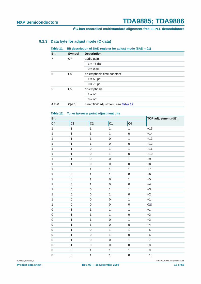
9.2.3 Data byte for adjust mode (C data)
Table 11. Bit description of SAD register for adjust mode (SAD = 01)
Bit Symbol Description
7 C7 audio gain
1 = −6 dB
0 = 0 dB
6 C6 de-emphasis time constant
1 = 50 µs
0 = 75 µs
5 C5 de-emphasis
1 = on
0 = off
4 to 0 C[4:0] tuner TOP adjustment; see Table 12
Table 12. Tuner takeover point adjustment bits
Bit TOP adjustment (dB)
C4 C3 C2 C1 C0
1 1 1 1 1 +15
1 1 1 1 0 +14
1 1 1 0 1 +13
1 1 1 0 0 +12
1 1 0 1 1 +11
1 1 0 1 0 +10
1 1 0 0 1 +9
1 1 0 0 0 +8
1 0 1 1 1 +7
1 0 1 1 0 +6
1 0 1 0 1 +5
1 0 1 0 0 +4
1 0 0 1 1 +3
1 0 0 1 0 +2
1 0 0 0 1 +1
1 0 0 0 0 0[1]
0 1 1 1 1 −1
0 1 1 1 0 −2
0 1 1 0 1 −3
0 1 1 0 0 −4
0 1 0 1 1 −5
0 1 0 1 0 −6
0 1 0 0 1 −7
0 1 0 0 0 −8
0 0 1 1 1 −9
0 0 1 1 0 −10
TDA9885_TDA9886_3 © NXP B.V. 2008. All rights reserved.
Product data sheet Rev. 03 — 16 December 2008 18 of 56

NXP Semiconductors TDA9885; TDA9886I2C-bus controlled multistandard alignment-free IF-PLL demodulators
[1] For 0 dB refer to Section 12 symbol QVTOP.
9.2.4 Data byte for data mode (E data)
[1] For positive modulation choose 6.5 MHz.
[1] The corresponding port function has to be disabled (set to ‘high-impedance’); see Table 10 and Tablenote 12 of Table 20.
0 0 1 0 1 −11
0 0 1 0 0 −12
0 0 0 1 1 −13
0 0 0 1 0 −14
0 0 0 0 1 −15
0 0 0 0 0 −16
Table 12. Tuner takeover point adjustment bits …continued
Bit TOP adjustment (dB)
C4 C3 C2 C1 C0
Table 13. Bit description of SAD register for data mode (SAD = 10)
Bit Symbol Description
7 E7 VIF AGC and port features; dependent on bit E5; see Table 14
6 E6 L standard PLL gating
1 = gating in case of 36 % positive modulation
0 = gating in case of 0 % positive modulation
5 E5 VIF, SIF and tuner minimum gain; dependent on bit E7; see Table 14
4 to 2 E[4:2] vision intermediate frequency selection; see Table 15
1 and 0 E[1:0] sound intercarrier frequency selection (sound 2nd IF)
00 = fFM = 4.5 MHz
01 = fFM = 5.5 MHz
10 = fFM = 6.0 MHz
11 = fFM = 6.5 MHz[1]
Table 14. Options in extended TV mode; bit B3 = 0 of SAD 00 register
Function Bit E7 = 0 Bit E7 = 1
Bit E5 = 0 Bit E5 = 1 Bit E5 = 0 Bit E5 = 1
Pin OP1 port function port function port function VIF-AGC external input[1]
Pin OP2 port function port function VIF-AGC output[1] port function
Gain normal gain minimum gain normal gain external gain
TDA9885_TDA9886_3 © NXP B.V. 2008. All rights reserved.
Product data sheet Rev. 03 — 16 December 2008 19 of 56

NXP Semiconductors TDA9885; TDA9886I2C-bus controlled multistandard alignment-free IF-PLL demodulators
[1] Pin SIOMAD can be used for the selection of the different NTSC standards without I2C-bus. With a resistoron pin SIOMAD, fVIF = 58.75 MHz; without a resistor on pin SIOMAD, fVIF = 45.75 MHz (NTSC-M).
Table 15. TV standard selection for VIF
Video IF select bits fVIF (MHz)
E4 E3 E2
0 0 0 58.75[1]
0 0 1 45.75[1]
0 1 0 38.9
0 1 1 38.0
1 0 0 33.9
1 0 1 33.4
1 1 0 not applicable
1 1 1 not applicable
Table 16. Data setting after power-on reset (default setting with a resistor on pin SIOMAD)
Register Byte
MSB LSB
7 6 5 4 3 2 1 0
Switching mode (B data) 1 1 0 1 0 1 1 0
Adjust mode (C data) 0 0 1 1 0 0 0 0
Data mode (E data) 0 0 0 0 0 0 0 0
Table 17. Data setting after power-on reset (default setting without a resistor onpin SIOMAD)
Register Byte
MSB LSB
7 6 5 4 3 2 1 0
Switching mode (B data) 1 1 0 1 0 1 1 0
Adjust mode (C data) 0 0 1 1 0 0 0 0
Data mode (E data) 0 0 0 0 0 1 0 0
TDA9885_TDA9886_3 © NXP B.V. 2008. All rights reserved.
Product data sheet Rev. 03 — 16 December 2008 20 of 56

NXP Semiconductors TDA9885; TDA9886I2C-bus controlled multistandard alignment-free IF-PLL demodulators
10. Limiting values
[1] Class C according to EIA/JESD22-A115.
[2] Class 2 according to JESD22-A114.
11. Thermal characteristics
Table 18. Limiting valuesIn accordance with the Absolute Maximum Rating System (IEC 60134).
Symbol Parameter Conditions Min Max Unit
VP supply voltage - 5.5 V
Vn voltage on
pins VIF1, VIF2, SIF1, SIF2,OP1, OP2, VP and FMPLL
0 VP V
pin TAGC 0 8.8 V
tsc short-circuit time to ground or VP - 10 s
Tstg storage temperature −25 +150 °C
Tamb ambient temperature TDA9885T (SO24),TDA9885TS (SSOP24),TDA9886T (SO24)and TDA9886TS (SSOP24)
−20 +70 °C
TDA9885HN (HVQFN32)and TDA9886HN (HVQFN32)
−20 +85 °C
Vesd electrostatic discharge voltage machine model [1] −400 +400 V
human body model [2] −4000 +3500 V
Table 19. Thermal characteristics
Symbol Parameter Conditions Typ Unit
Rth(j-a) thermal resistance from junction to ambient in free air
TDA9885T (SO24) 76 K/W
TDA9885TS (SSOP24) 118 K/W
TDA9885HN (HVQFN32) 40 K/W
TDA9886T (SO24) 76 K/W
TDA9886TS (SSOP24) 118 K/W
TDA9886HN (HVQFN32) 40 K/W
TDA9885_TDA9886_3 © NXP B.V. 2008. All rights reserved.
Product data sheet Rev. 03 — 16 December 2008 21 of 56
NXP Semiconductors TDA9885; TDA9886I2C-bus controlled multistandard alignment-free IF-PLL demodulators
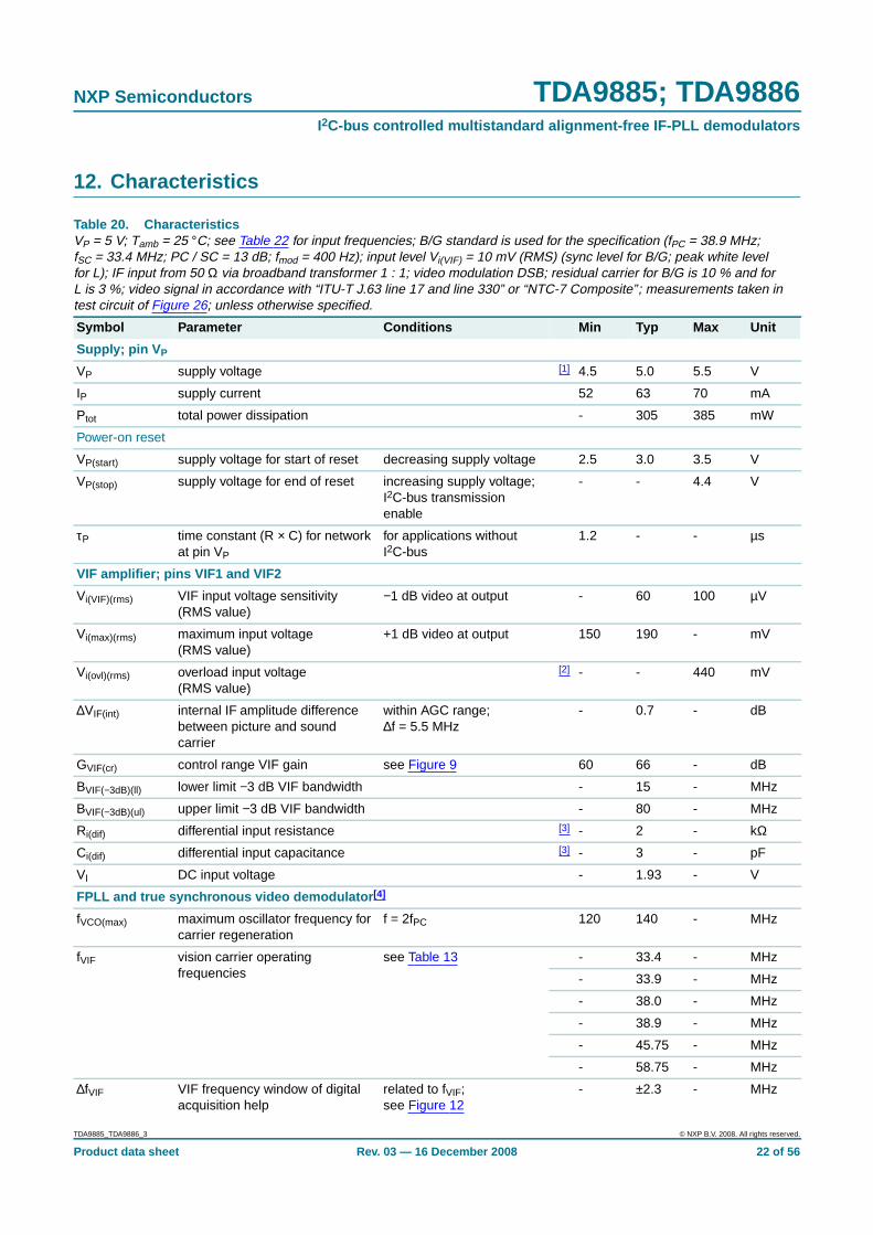
12. Characteristics
Table 20. CharacteristicsVP = 5 V; Tamb = 25 °C; see Table 22 for input frequencies; B/G standard is used for the specification (fPC = 38.9 MHz;fSC = 33.4 MHz; PC / SC = 13 dB; fmod = 400 Hz); input level Vi(VIF) = 10 mV (RMS) (sync level for B/G; peak white levelfor L); IF input from 50 Ω via broadband transformer 1 : 1; video modulation DSB; residual carrier for B/G is 10 % and forL is 3 %; video signal in accordance with “ITU-T J.63 line 17 and line 330” or “NTC-7 Composite”; measurements taken intest circuit of Figure 26; unless otherwise specified.
Symbol Parameter Conditions Min Typ Max Unit
Supply; pin V P
VP supply voltage [1] 4.5 5.0 5.5 V
IP supply current 52 63 70 mA
Ptot total power dissipation - 305 385 mW
Power-on reset
VP(start) supply voltage for start of reset decreasing supply voltage 2.5 3.0 3.5 V
VP(stop) supply voltage for end of reset increasing supply voltage;I2C-bus transmissionenable
- - 4.4 V
τP time constant (R × C) for networkat pin VP
for applications withoutI2C-bus
1.2 - - µs
VIF amplifier; pins VIF1 and VIF2
Vi(VIF)(rms) VIF input voltage sensitivity(RMS value)
−1 dB video at output - 60 100 µV
Vi(max)(rms) maximum input voltage(RMS value)
+1 dB video at output 150 190 - mV
Vi(ovl)(rms) overload input voltage(RMS value)
[2] - - 440 mV
∆VIF(int) internal IF amplitude differencebetween picture and soundcarrier
within AGC range;∆f = 5.5 MHz
- 0.7 - dB
GVIF(cr) control range VIF gain see Figure 9 60 66 - dB
BVIF(−3dB)(ll) lower limit −3 dB VIF bandwidth - 15 - MHz
BVIF(−3dB)(ul) upper limit −3 dB VIF bandwidth - 80 - MHz
Ri(dif) differential input resistance [3] - 2 - kΩ
Ci(dif) differential input capacitance [3] - 3 - pF
VI DC input voltage - 1.93 - V
FPLL and true synchronous video demodulator [4]
fVCO(max) maximum oscillator frequency forcarrier regeneration
f = 2fPC 120 140 - MHz
fVIF vision carrier operatingfrequencies
see Table 13 - 33.4 - MHz
- 33.9 - MHz
- 38.0 - MHz
- 38.9 - MHz
- 45.75 - MHz
- 58.75 - MHz
∆fVIF VIF frequency window of digitalacquisition help
related to fVIF;see Figure 12
- ±2.3 - MHz
TDA9885_TDA9886_3 © NXP B.V. 2008. All rights reserved.
Product data sheet Rev. 03 — 16 December 2008 22 of 56

NXP Semiconductors TDA9885; TDA9886I2C-bus controlled multistandard alignment-free IF-PLL demodulators
tacq acquisition time BL = 70 kHz [5] - - 30 ms
Vi(lock)(rms) input voltage sensitivity for PLL tobe locked (RMS value)
measured on pins VIF1and VIF2; maximumIF gain
- 30 70 µV
Tcy(dah) digital acquisition help cycle time - 64 - µs
KO(VIF) VIF VCO steepness definition: ∆fVIF / ∆VVPLL - 20 - MHz/V
KD(VIF) VIF phase detector steepness definition: ∆IVPLL / ∆ϕVIF - 23 - µA/rad
Video output 2 V; pin CVBS
Normal mode (sound carrier trap active) and sound carrier on
Vo(v)(p-p) video output voltage(peak-to-peak value)
see Figure 7 1.7 2.0 2.3 V
∆Vo video output voltage difference difference betweenL and B/G standard
−12 - +12 %
V/S ratio between video(black-to-white) and sync level
1.90 2.33 3.00
Vsync sync voltage level 1.0 1.2 1.4 V
Vclip(u) upper video clipping voltage level VP − 1.1 VP − 1 - V
Vclip(l) lower video clipping voltage level - 0.7 0.9 V
Ro output resistance [3] - - 30 Ω
Ibias(int) internal bias current (DC) for emitter-follower 1.5 2.0 - mA
Isink(o)(max) maximum output sink current AC and DC 1 - - mA
Isource(o)(max) maximum output source current AC and DC 3.9 - - mA
∆Vo(CVBS) deviation of CVBS output voltage 50 dB gain control - - 0.5 dB
30 dB gain control - - 0.1 dB
∆Vo(bl) black level tilt negative modulation - - 1 %
∆Vo(bl)(v) vertical black level tilt for worstcase in L standard
vision carrier modulated bytest line (VITS) only
- - 3 %
Gdif differential gain “ITU-T J.63 line 330” [6]
B/G standard - - 5 %
L standard - - 7 %
ϕdif differential phase “ITU-T J.63 line 330” - 2 4 deg
S/NW weighted signal-to-noise ratio unified weighting filter(“ITU-T J.61”);see Figure 13
[7] 56 59 - dB
S/NUW unweighted signal-to-noise ratio [7] 47 51 - dB
αIM(blue) intermodulation attenuation at‘blue’
see Figure 14 [8]
f = 1.1 MHz 58 64 - dB
f = 3.3 MHz 58 64 - dB
Table 20. Characteristics …continuedVP = 5 V; Tamb = 25 °C; see Table 22 for input frequencies; B/G standard is used for the specification (fPC = 38.9 MHz;fSC = 33.4 MHz; PC / SC = 13 dB; fmod = 400 Hz); input level Vi(VIF) = 10 mV (RMS) (sync level for B/G; peak white levelfor L); IF input from 50 Ω via broadband transformer 1 : 1; video modulation DSB; residual carrier for B/G is 10 % and forL is 3 %; video signal in accordance with “ITU-T J.63 line 17 and line 330” or “NTC-7 Composite”; measurements taken intest circuit of Figure 26; unless otherwise specified.
Symbol Parameter Conditions Min Typ Max Unit
TDA9885_TDA9886_3 © NXP B.V. 2008. All rights reserved.
Product data sheet Rev. 03 — 16 December 2008 23 of 56

NXP Semiconductors TDA9885; TDA9886I2C-bus controlled multistandard alignment-free IF-PLL demodulators
αIM(yellow) intermodulation attenuation at‘yellow’
see Figure 14 [8]
f = 1.1 MHz 60 66 - dB
f = 3.3 MHz 59 65 - dB
∆Vr(PC)(rms) residual picture carrier(RMS value)
fundamental wave andharmonics
- 2 5 mV
∆funw(p-p) robustness for unwantedfrequency deviation of picturecarrier (peak-to-peak value)
3 % residual carrier;50 % serration pulses;L standard
[3] - - 12 kHz
∆ϕ robustness for modulatorimbalance
0 % residual carrier;50 % serration pulses;L standard; L-gating = 0 %
[3] - - 3 %
αH suppression of video signalharmonics
AC load: CL < 20 pF,RL > 1 kΩ
[9] 35 40 - dB
αspur suppression of spurious elements [10] 40 - - dB
PSRRCVBS power supply ripple rejection onpin CVBS
fripple = 70 Hz; video signal;grey level; positive andnegative modulation;see Figure 8
20 25 - dB
M/N standard including Korea; see Figure 15
Bv(−3dB)(trap) −3 dB video bandwidth includingsound carrier trap
ftrap = 4.5 MHz [11] 3.95 4.05 - MHz
αSC1 attenuation at first sound carrier f = 4.5 MHz 30 36 - dB
αSC1(60kHz) attenuation at first sound carrierfSC1 ± 60 kHz
f = 4.5 MHz 21 27 - dB
αSC2 attenuation at second soundcarrier
f = 4.724 MHz 21 27 - dB
αSC2(60kHz) attenuation at second soundcarrier fSC2 ± 60 kHz
f = 4.724 MHz 15 21 - dB
td(g)(cc) group delay at color carrierfrequency
f = 3.58 MHz;see Figure 16
110 180 250 ns
B/G standard; see Figure 17
Bv(−3dB)(trap) −3 dB video bandwidth includingsound carrier trap
ftrap = 5.5 MHz [11] 4.90 5.00 - MHz
αSC1 attenuation at first sound carrier f = 5.5 MHz 30 36 - dB
αSC1(60kHz) attenuation at first sound carrierfSC1 ± 60 kHz
f = 5.5 MHz 24 30 - dB
αSC2 attenuation at second soundcarrier
f = 5.742 MHz 21 27 - dB
αSC2(60kHz) attenuation at second soundcarrier fSC2 ± 60 kHz
f = 5.742 MHz 15 21 - dB
td(g)(cc) group delay at color carrierfrequency
f = 4.43 MHz;see Figure 18
110 180 250 ns
Table 20. Characteristics …continuedVP = 5 V; Tamb = 25 °C; see Table 22 for input frequencies; B/G standard is used for the specification (fPC = 38.9 MHz;fSC = 33.4 MHz; PC / SC = 13 dB; fmod = 400 Hz); input level Vi(VIF) = 10 mV (RMS) (sync level for B/G; peak white levelfor L); IF input from 50 Ω via broadband transformer 1 : 1; video modulation DSB; residual carrier for B/G is 10 % and forL is 3 %; video signal in accordance with “ITU-T J.63 line 17 and line 330” or “NTC-7 Composite”; measurements taken intest circuit of Figure 26; unless otherwise specified.
Symbol Parameter Conditions Min Typ Max Unit
TDA9885_TDA9886_3 © NXP B.V. 2008. All rights reserved.
Product data sheet Rev. 03 — 16 December 2008 24 of 56

NXP Semiconductors TDA9885; TDA9886I2C-bus controlled multistandard alignment-free IF-PLL demodulators
I standard; see Figure 19
Bv(−3dB)(trap) −3 dB video bandwidth includingsound carrier trap
ftrap = 6.0 MHz [11] 5.40 5.50 - MHz
αSC1 attenuation at first sound carrier f = 6.0 MHz 26 32 - dB
αSC1(60kHz) attenuation at first sound carrierfSC1 ± 60 kHz
f = 6.0 MHz 20 26 - dB
αSC2 attenuation at second soundcarrier
f = 6.55 MHz 12 18 - dB
αSC2(60kHz) attenuation at second soundcarrier fSC2 ± 60 kHz
f = 6.55 MHz 10 15 - dB
td(g)(cc) group delay at color carrierfrequency
f = 4.43 MHz - 90 160 ns
D/K standard; see Figure 20
Bv(−3dB)(trap) −3 dB video bandwidth includingsound carrier trap
ftrap = 6.5 MHz [11] 5.50 5.95 - MHz
αSC1 attenuation at first sound carrier f = 6.5 MHz 26 32 - dB
αSC1(60kHz) attenuation at first sound carrierfSC1 ± 60 kHz
f = 6.5 MHz 20 26 - dB
αSC2 attenuation at second soundcarrier
f = 6.742 MHz 18 24 - dB
αSC2(60kHz) attenuation at second soundcarrier fSC2 ± 60 kHz
f = 6.742 MHz 13 18 - dB
td(g)(cc) group delay at color carrierfrequency
f = 4.28 MHz - 60 130 ns
Video output 1.1 V; pin CVBS
Trap bypass mode and sound carrier off[12]
Vo(v)(p-p) video output voltage(peak-to-peak value)
see Figure 7 0.95 1.10 1.25 V
Vsync sync voltage level 1.35 1.5 1.6 V
Vclip(u) upper video clipping voltage level 3.5 3.6 - V
Vclip(l) lower video clipping voltage level - 0.9 1.0 V
Bv(−1dB) −1 dB video bandwidth AC load: CL < 20 pF,RL > 1 kΩ
5 6 - MHz
Bv(−3dB) −3 dB video bandwidth AC load: CL < 20 pF,RL > 1 kΩ
7 8 - MHz
S/NW weighted signal-to-noise ratio unified weighting filter(“ITU-T J.61”);see Figure 13
[7] 56 59 - dB
S/NUW unweighted signal-to-noise ratio [7] 48 52 - dB
Table 20. Characteristics …continuedVP = 5 V; Tamb = 25 °C; see Table 22 for input frequencies; B/G standard is used for the specification (fPC = 38.9 MHz;fSC = 33.4 MHz; PC / SC = 13 dB; fmod = 400 Hz); input level Vi(VIF) = 10 mV (RMS) (sync level for B/G; peak white levelfor L); IF input from 50 Ω via broadband transformer 1 : 1; video modulation DSB; residual carrier for B/G is 10 % and forL is 3 %; video signal in accordance with “ITU-T J.63 line 17 and line 330” or “NTC-7 Composite”; measurements taken intest circuit of Figure 26; unless otherwise specified.
Symbol Parameter Conditions Min Typ Max Unit
TDA9885_TDA9886_3 © NXP B.V. 2008. All rights reserved.
Product data sheet Rev. 03 — 16 December 2008 25 of 56
NXP Semiconductors TDA9885; TDA9886I2C-bus controlled multistandard alignment-free IF-PLL demodulators
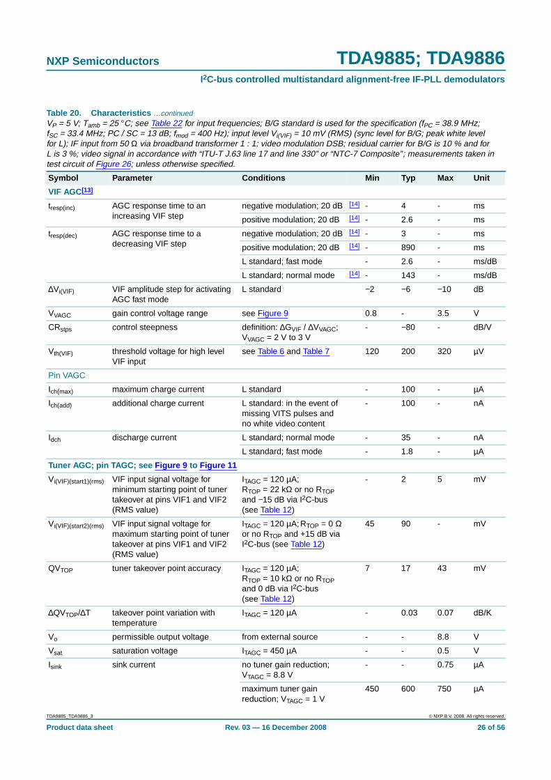
VIF AGC[13]
tresp(inc) AGC response time to anincreasing VIF step
negative modulation; 20 dB [14] - 4 - ms
positive modulation; 20 dB [14] - 2.6 - ms
tresp(dec) AGC response time to adecreasing VIF step
negative modulation; 20 dB [14] - 3 - ms
positive modulation; 20 dB [14] - 890 - ms
L standard; fast mode - 2.6 - ms/dB
L standard; normal mode [14] - 143 - ms/dB
∆Vi(VIF) VIF amplitude step for activatingAGC fast mode
L standard −2 −6 −10 dB
VVAGC gain control voltage range see Figure 9 0.8 - 3.5 V
CRstps control steepness definition: ∆GVIF / ∆VVAGC;VVAGC = 2 V to 3 V
- −80 - dB/V
Vth(VIF) threshold voltage for high levelVIF input
see Table 6 and Table 7 120 200 320 µV
Pin VAGC
Ich(max) maximum charge current L standard - 100 - µA
Ich(add) additional charge current L standard: in the event ofmissing VITS pulses andno white video content
- 100 - nA
Idch discharge current L standard; normal mode - 35 - nA
L standard; fast mode - 1.8 - µA
Tuner AGC; pin TAGC; see Figure 9 to Figure 11
Vi(VIF)(start1)(rms) VIF input signal voltage forminimum starting point of tunertakeover at pins VIF1 and VIF2(RMS value)
ITAGC = 120 µA;RTOP = 22 kΩ or no RTOPand −15 dB via I2C-bus(see Table 12)
- 2 5 mV
Vi(VIF)(start2)(rms) VIF input signal voltage formaximum starting point of tunertakeover at pins VIF1 and VIF2(RMS value)
ITAGC = 120 µA; RTOP = 0 Ωor no RTOP and +15 dB viaI2C-bus (see Table 12)
45 90 - mV
QVTOP tuner takeover point accuracy ITAGC = 120 µA;RTOP = 10 kΩ or no RTOPand 0 dB via I2C-bus(see Table 12)
7 17 43 mV
∆QVTOP/∆T takeover point variation withtemperature
ITAGC = 120 µA - 0.03 0.07 dB/K
Vo permissible output voltage from external source - - 8.8 V
Vsat saturation voltage ITAGC = 450 µA - - 0.5 V
Isink sink current no tuner gain reduction;VTAGC = 8.8 V
- - 0.75 µA
maximum tuner gainreduction; VTAGC = 1 V
450 600 750 µA
Table 20. Characteristics …continuedVP = 5 V; Tamb = 25 °C; see Table 22 for input frequencies; B/G standard is used for the specification (fPC = 38.9 MHz;fSC = 33.4 MHz; PC / SC = 13 dB; fmod = 400 Hz); input level Vi(VIF) = 10 mV (RMS) (sync level for B/G; peak white levelfor L); IF input from 50 Ω via broadband transformer 1 : 1; video modulation DSB; residual carrier for B/G is 10 % and forL is 3 %; video signal in accordance with “ITU-T J.63 line 17 and line 330” or “NTC-7 Composite”; measurements taken intest circuit of Figure 26; unless otherwise specified.
Symbol Parameter Conditions Min Typ Max Unit
TDA9885_TDA9886_3 © NXP B.V. 2008. All rights reserved.
Product data sheet Rev. 03 — 16 December 2008 26 of 56

NXP Semiconductors TDA9885; TDA9886I2C-bus controlled multistandard alignment-free IF-PLL demodulators
∆GIF IF slip by automatic gain control tuner gain current from20 % to 80 %
3 5 8 dB
AFC circuit; pin AFC [15] [16]; see Figure 12
Vsat(ul) upper limit saturation voltage VP − 0.6 VP − 0.3 - V
Vsat(ll) lower limit saturation voltage - 0.3 0.6 V
Isource(o) output source current 160 200 240 µA
Isink(o) output sink current 160 200 240 µA
AFCstps AFC control steepness definition: ∆IAFC / ∆fVIF 0.85 1.05 1.25 µA/kHz
QfVIF(a) analog accuracy of AFC circuit IAFC = 0 µA; fREF = 4 MHz −20 - +20 kHz
QfVIF(d) digital accuracy of AFC circuit viaI2C-bus
IAFC = 0 µA; fREF = 4 MHz;1 digit = 25 kHz
−20− 1 digit
- +20+ 1 digit
kHz
SIF amplifier; pins SIF1 and SIF2
Vi(SIF)(rms) SIF input voltage sensitivity(RMS value)
FM mode; −3 dB atintercarrier outputpin SIOMAD
- 30 70 µV
AM mode; −3 dB atAF output pin AUD
- 70 100 µV
Vi(max)(rms) maximum input voltage(RMS value)
FM mode; +1 dB atintercarrier outputpin SIOMAD
50 70 - mV
AM mode; +1 dB atAF output pin AUD
80 140 - mV
Vi(ovl)(rms) overload input voltage(RMS value)
[2] - - 320 mV
GSIF(cr) SIF gain control range FM and AM mode;see Figure 11
60 66 - dB
BSIF(−3dB)(ll) lower limit −3 dB SIF bandwidth - 15 - MHz
BSIF(−3dB)(ul) upper limit −3 dB SIF bandwidth - 80 - MHz
Ri(dif) differential input resistance [3] - 2 - kΩ
Ci(dif) differential input capacitance [3] - 3 - pF
VI DC input voltage - 1.93 - V
SIF-AGC detector
tresp AGC response time to anincreasing or decreasing SIF stepof 20 dB
FM or AM fast step
increasing - 8 - ms
decreasing - 25 - ms
AM slow step
increasing - 80 - ms
decreasing - 250 - ms
Table 20. Characteristics …continuedVP = 5 V; Tamb = 25 °C; see Table 22 for input frequencies; B/G standard is used for the specification (fPC = 38.9 MHz;fSC = 33.4 MHz; PC / SC = 13 dB; fmod = 400 Hz); input level Vi(VIF) = 10 mV (RMS) (sync level for B/G; peak white levelfor L); IF input from 50 Ω via broadband transformer 1 : 1; video modulation DSB; residual carrier for B/G is 10 % and forL is 3 %; video signal in accordance with “ITU-T J.63 line 17 and line 330” or “NTC-7 Composite”; measurements taken intest circuit of Figure 26; unless otherwise specified.
Symbol Parameter Conditions Min Typ Max Unit
TDA9885_TDA9886_3 © NXP B.V. 2008. All rights reserved.
Product data sheet Rev. 03 — 16 December 2008 27 of 56

NXP Semiconductors TDA9885; TDA9886I2C-bus controlled multistandard alignment-free IF-PLL demodulators
Single reference QSS intercarrier mixer; pin SIOMAD
Vo(intc)(rms) IF intercarrier output level(RMS value)
QSS mode; SC1; SC2 off 90 140 180 mV
L standard;without modulation
90 140 180 mV
intercarrier mode;PC / SC1 = 20 dB; SC2 off
[17] - 75 - mV
Bintc(−3dB)(ul) upper limit −3 dB intercarrierbandwidth
12 15 - MHz
∆Vr(SC)(rms) residual sound carrier(RMS value)
fundamental wave andharmonics
QSS mode - 2 5 mV
intercarrier mode - 2 5 mV
∆Vr(PC)(rms) residual picture carrier(RMS value)
fundamental wave andharmonics
QSS mode - 2 5 mV
intercarrier mode - 5 20 mV
αH suppression of video signalharmonics
intercarrier mode;fvideo = 5 MHz
35 40 - dB
Ro output resistance [3] - - 30 Ω
VO DC output voltage - 2 - V
Ibias(int) internal bias current (DC) for emitter-follower 0.90 1.15 - mA
Isink(o)(max) maximum output sink current AC 0.6 0.8 - mA
Isource(o)(max) maximum output source current AC 0.6 0.8 - mA
Isource(o) output source current DC; MAD2 activated [18] 0.75 0.93 1.20 mA
FM-PLL demodulator [16] [19] [20] [21] [22] [23]
Sound intercarrier output; pin SIOMAD
VFM(rms) IF intercarrier level for gaincontrolled operation of FM PLL(RMS value)
corresponding PC / SCratio at input pins VIF1and VIF2 is 7 dB to 47 dB
3.2 - 320 mV
VFM(lock)(rms) IF intercarrier level for lock-in ofPLL (RMS value)
- - 2 mV
VFM(det)(rms) IF intercarrier level for FM carrierdetect (RMS value)
see Table 7 - - 2.3 mV
fFM sound intercarrier operatingFM frequencies
see Table 13 [24] - 4.5 - MHz
- 5.5 - MHz
- 6.0 - MHz
- 6.5 - MHz
Table 20. Characteristics …continuedVP = 5 V; Tamb = 25 °C; see Table 22 for input frequencies; B/G standard is used for the specification (fPC = 38.9 MHz;fSC = 33.4 MHz; PC / SC = 13 dB; fmod = 400 Hz); input level Vi(VIF) = 10 mV (RMS) (sync level for B/G; peak white levelfor L); IF input from 50 Ω via broadband transformer 1 : 1; video modulation DSB; residual carrier for B/G is 10 % and forL is 3 %; video signal in accordance with “ITU-T J.63 line 17 and line 330” or “NTC-7 Composite”; measurements taken intest circuit of Figure 26; unless otherwise specified.
Symbol Parameter Conditions Min Typ Max Unit
TDA9885_TDA9886_3 © NXP B.V. 2008. All rights reserved.
Product data sheet Rev. 03 — 16 December 2008 28 of 56
NXP Semiconductors TDA9885; TDA9886I2C-bus controlled multistandard alignment-free IF-PLL demodulators
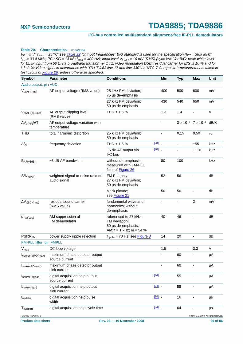
Audio output; pin AUD
Vo(AF)(rms) AF output voltage (RMS value) 25 kHz FM deviation;75 µs de-emphasis
400 500 600 mV
27 kHz FM deviation;50 µs de-emphasis
430 540 650 mV
Vo(AF)(cl)(rms) AF output clipping level(RMS value)
THD < 1.5 % 1.3 1.4 - V
∆Vo(AF)/∆T AF output voltage variation withtemperature
- 3 × 10⁻³ 7 × 10⁻³ dB/K
THD total harmonic distortion 25 kHz FM deviation;50 µs de-emphasis
- 0.15 0.50 %
∆fAF frequency deviation THD < 1.5 % [20] - - ±55 kHz
−6 dB AF output viaI2C-bus
[20] - - ±110 kHz
BAF(−3dB) −3 dB AF bandwidth without de-emphasis;measured with FM-PLLfilter of Figure 26
80 100 - kHz
S/NW(AF) weighted signal-to-noise ratio ofaudio signal
FM PLL only;27 kHz FM deviation;50 µs de-emphasis
52 56 - dB
black picture;see Figure 21
50 56 - dB
∆Vr(SC)(rms) residual sound carrier(RMS value)
fundamental wave andharmonics; withoutde-emphasis
- - 2 mV
αAM(sup) AM suppression ofFM demodulator
referenced to 27 kHzFM deviation;50 µs de-emphasis;AM: f = 1 kHz; m = 54 %
40 46 - dB
PSRRFM power supply ripple rejection fripple = 70 Hz; see Figure 8 14 20 - dB
FM-PLL filter; pin FMPLL
Vloop DC loop voltage 1.5 - 3.3 V
Isource(o)PD(max) maximum phase detector outputsource current
- 60 - µA
Isink(o)PD(max) maximum phase detector outputsink current
- 60 - µA
Isource(o)(dah) digital acquisition help outputsource current
[24] - 55 - µA
Isink(o)(dah) digital acquisition help outputsink current
[24] - 55 - µA
tw(dah) digital acquisition help pulsewidth
[24] - 16 - µs
Tcy(dah) digital acquisition help cycle time [24] - 64 - µs
Table 20. Characteristics …continuedVP = 5 V; Tamb = 25 °C; see Table 22 for input frequencies; B/G standard is used for the specification (fPC = 38.9 MHz;fSC = 33.4 MHz; PC / SC = 13 dB; fmod = 400 Hz); input level Vi(VIF) = 10 mV (RMS) (sync level for B/G; peak white levelfor L); IF input from 50 Ω via broadband transformer 1 : 1; video modulation DSB; residual carrier for B/G is 10 % and forL is 3 %; video signal in accordance with “ITU-T J.63 line 17 and line 330” or “NTC-7 Composite”; measurements taken intest circuit of Figure 26; unless otherwise specified.
Symbol Parameter Conditions Min Typ Max Unit
TDA9885_TDA9886_3 © NXP B.V. 2008. All rights reserved.
Product data sheet Rev. 03 — 16 December 2008 29 of 56

NXP Semiconductors TDA9885; TDA9886I2C-bus controlled multistandard alignment-free IF-PLL demodulators
KO(FM) VCO steepness definition: ∆fFM / ∆VFMPLL - 3.3 - MHz/V
KD(FM) phase detector steepness definition: ∆IFMPLL / ∆ϕFM - 4 - µA/rad
Audio amplifier
De-emphasis network; pin DEEM
Ro output resistance 50 µs de-emphasis;see Table 11
4.4 5.0 5.6 kΩ
75 µs de-emphasis;see Table 11
6.6 7.5 8.4 kΩ
VAF(rms) audio signal (RMS value) fAF = 400 Hz;VAUD = 500 mV
- 170 - mV
VO DC output voltage - 2.37 - V
AF decoupling; pin AFD
Vdec decoupling voltage (DC) dependent on fFMintercarrier frequency
1.5 - 3.3 V
IL leakage current ∆VO(AUD) < ±50 mV - - ±25 nA
Ich(max) maximum charge current 1.15 1.50 1.85 µA
Idch(max) maximum discharge current 1.15 1.50 1.85 µA
Audio output; pin AUD
Ro output resistance [3] - - 300 Ω
VO(AUD) DC output voltage - 2.37 - V
RL load resistance AC-coupled 10 - - kΩ
RL(DC) DC load resistance 100 - - kΩ
CL load capacitance - - 1.5 nF
BAF(−3dB)(ul) upper limit −3 dB AF bandwidth ofaudio amplifier
150 - - kHz
BAF(−3dB)(ll) lower limit −3 dB AF bandwidth ofaudio amplifier
[21] - - 20 Hz
αmute mute attenuation of AF signal via I2C-bus 70 75 - dB
∆Vjump DC jump voltage for switchingAF output to mute state or viceversa
activated by digitalacquisition help or viaI2C-bus mute
- ±50 ±150 mV
Table 20. Characteristics …continuedVP = 5 V; Tamb = 25 °C; see Table 22 for input frequencies; B/G standard is used for the specification (fPC = 38.9 MHz;fSC = 33.4 MHz; PC / SC = 13 dB; fmod = 400 Hz); input level Vi(VIF) = 10 mV (RMS) (sync level for B/G; peak white levelfor L); IF input from 50 Ω via broadband transformer 1 : 1; video modulation DSB; residual carrier for B/G is 10 % and forL is 3 %; video signal in accordance with “ITU-T J.63 line 17 and line 330” or “NTC-7 Composite”; measurements taken intest circuit of Figure 26; unless otherwise specified.
Symbol Parameter Conditions Min Typ Max Unit
TDA9885_TDA9886_3 © NXP B.V. 2008. All rights reserved.
Product data sheet Rev. 03 — 16 December 2008 30 of 56
NXP Semiconductors TDA9885; TDA9886I2C-bus controlled multistandard alignment-free IF-PLL demodulators
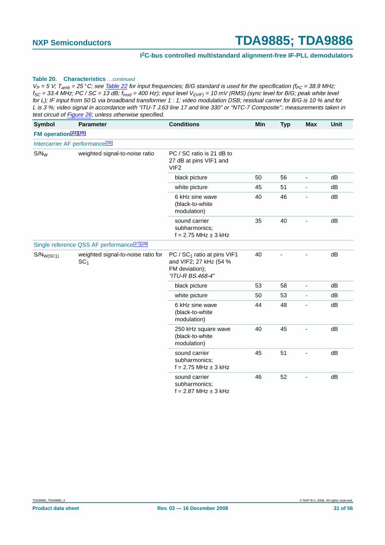
FM operation [22] [25]
Intercarrier AF performance[26]
S/NW weighted signal-to-noise ratio PC / SC ratio is 21 dB to27 dB at pins VIF1 andVIF2
black picture 50 56 - dB
white picture 45 51 - dB
6 kHz sine wave(black-to-whitemodulation)
40 46 - dB
sound carriersubharmonics;f = 2.75 MHz ± 3 kHz
35 40 - dB
Single reference QSS AF performance[27][28]
S/NW(SC1) weighted signal-to-noise ratio forSC1
PC / SC1 ratio at pins VIF1and VIF2; 27 kHz (54 %FM deviation);“ITU-R BS.468-4”
40 - - dB
black picture 53 58 - dB
white picture 50 53 - dB
6 kHz sine wave(black-to-whitemodulation)
44 48 - dB
250 kHz square wave(black-to-whitemodulation)
40 45 - dB
sound carriersubharmonics;f = 2.75 MHz ± 3 kHz
45 51 - dB
sound carriersubharmonics;f = 2.87 MHz ± 3 kHz
46 52 - dB
Table 20. Characteristics …continuedVP = 5 V; Tamb = 25 °C; see Table 22 for input frequencies; B/G standard is used for the specification (fPC = 38.9 MHz;fSC = 33.4 MHz; PC / SC = 13 dB; fmod = 400 Hz); input level Vi(VIF) = 10 mV (RMS) (sync level for B/G; peak white levelfor L); IF input from 50 Ω via broadband transformer 1 : 1; video modulation DSB; residual carrier for B/G is 10 % and forL is 3 %; video signal in accordance with “ITU-T J.63 line 17 and line 330” or “NTC-7 Composite”; measurements taken intest circuit of Figure 26; unless otherwise specified.
Symbol Parameter Conditions Min Typ Max Unit
TDA9885_TDA9886_3 © NXP B.V. 2008. All rights reserved.
Product data sheet Rev. 03 — 16 December 2008 31 of 56
NXP Semiconductors TDA9885; TDA9886I2C-bus controlled multistandard alignment-free IF-PLL demodulators
S/NW(SC2) weighted signal-to-noise ratio forSC2
PC / SC2 ratio at pins VIF1and VIF2; 27 kHz (54 %FM deviation);“ITU-R BS.468-4”
40 - - dB
black picture 48 55 - dB
white picture 46 51 - dB
6 kHz sine wave(black-to-whitemodulation)
42 46 - dB
250 kHz square wave(black-to-whitemodulation)
29 34 - dB
sound carriersubharmonics;f = 2.75 MHz ± 3 kHz
44 50 - dB
sound carriersubharmonics;f = 2.87 MHz ± 3 kHz
45 51 - dB
AM operation
L standard; pin AUD[29]; see Figure 22 and Figure 23
Vo(AF)(rms) AF output voltage (RMS value) 54 % AM modulation 400 500 600 mV
THD total harmonic distortion 54 % AM modulation - 0.5 1.0 %
BAF(−3dB) −3 dB AF bandwidth 100 125 - kHz
S/NW(AF) weighted signal-to-noise ratio ofaudio signal
in accordance with“ITU-R BS.468-4”
45 50 - dB
VO(AUD) DC potential voltage - 2.37 - V
PSRRAM power supply ripple rejection see Figure 8 20 26 - dB
Reference frequency input; pin REF
VI DC input voltage 2.3 2.6 2.9 V
Ri input resistance [3] - 5 - kΩ
Rxtal resonance resistance of crystal operation as crystaloscillator
- - 200 Ω
Cx pull-up/down capacitance [30] - - - pF
fref reference signal frequency [31] - 4 - MHz
∆fref tolerance of reference signalfrequency
[16] - - ±0.1 %
Vref(rms) reference signal voltage(RMS value)
operation as input terminal 80 - 400 mV
Ro(ref) output resistance of referencesignal source
- - 4.7 kΩ
CK decoupling capacitance toexternal reference signal source
operation as input terminal 22 100 - pF
Table 20. Characteristics …continuedVP = 5 V; Tamb = 25 °C; see Table 22 for input frequencies; B/G standard is used for the specification (fPC = 38.9 MHz;fSC = 33.4 MHz; PC / SC = 13 dB; fmod = 400 Hz); input level Vi(VIF) = 10 mV (RMS) (sync level for B/G; peak white levelfor L); IF input from 50 Ω via broadband transformer 1 : 1; video modulation DSB; residual carrier for B/G is 10 % and forL is 3 %; video signal in accordance with “ITU-T J.63 line 17 and line 330” or “NTC-7 Composite”; measurements taken intest circuit of Figure 26; unless otherwise specified.
Symbol Parameter Conditions Min Typ Max Unit
TDA9885_TDA9886_3 © NXP B.V. 2008. All rights reserved.
Product data sheet Rev. 03 — 16 December 2008 32 of 56
NXP Semiconductors TDA9885; TDA9886I2C-bus controlled multistandard alignment-free IF-PLL demodulators
[1] Values of video and sound parameters can be decreased at VP = 4.5 V.
[2] Level headroom for input level jumps during gain control setting.
[3] This parameter is not tested during the production and is only given as application information for designing the receiver circuit.
[4] Loop bandwidth BL = 70 kHz (damping factor d = 1.9; calculated with sync level within gain control range). Calculation of the VIF-PLLfilter can be done by use of the following formula:
, valid for d ≥ 1.2
,
where:
KO is the VCO steepness or ; KD is the phase detector steepness ;
R is the loop resistor (Ω); C is the loop capacitor (F); BL−3dB is the loop bandwidth for −3 dB (Hz); d is the damping factor.
[5] Vi(VIF) = 10 mV (RMS); ∆f = 1 MHz (VCO frequency offset related to the picture carrier frequency); white picture video modulation.
[6] Condition: luminance range (5 steps) from 0 % to 100 %.
[7] S/N is the ratio of black-to-white amplitude to the noise voltage (RMS value measured on pin CVBS and tested at video black level,‘quiet line’). Noise analyzer settings: B = 5 MHz, 200 kHz high-pass and sound carrier trap on. In case of S/NW weighted in accordancewith “ITU-T J.61”. Measurements taken for B/G standard.
[8] The intermodulation figures are defined for:
a) f = 1.1 MHz (referenced to black and white signal) as
b) f = 3.3 MHz (referenced to color carrier) as
I2C-bus transceiver; pins SDA and SCL [32] [33]
fSCL SCL clock frequency 0 - 400 kHz
VIH HIGH-level input voltage 3 - VCC V
VIL LOW-level input voltage −0.3 - +1.5 V
IIH HIGH-level input current −10 - +10 µA
IIL LOW-level input current −10 - +10 µA
VOL LOW-level output voltage IOL = 3 mA - - 0.4 V
Isink(o) output sink current VP = 0 V - - 10 µA
Isource(o) output source current VP = 0 V - - 10 µA
Output ports; pins OP1 and OP2 [34]
VOL LOW-level output voltage IOL = 2 mA (sink current) - - 0.4 V
VOH HIGH-level output voltage - - 6 V
Isink(o) output sink current - - 2 mA
Io(max) maximum output current sink or source; pin OP2functions as VIF-AGCoutput
- - 10 µA
Table 20. Characteristics …continuedVP = 5 V; Tamb = 25 °C; see Table 22 for input frequencies; B/G standard is used for the specification (fPC = 38.9 MHz;fSC = 33.4 MHz; PC / SC = 13 dB; fmod = 400 Hz); input level Vi(VIF) = 10 mV (RMS) (sync level for B/G; peak white levelfor L); IF input from 50 Ω via broadband transformer 1 : 1; video modulation DSB; residual carrier for B/G is 10 % and forL is 3 %; video signal in accordance with “ITU-T J.63 line 17 and line 330” or “NTC-7 Composite”; measurements taken intest circuit of Figure 26; unless otherwise specified.
Symbol Parameter Conditions Min Typ Max Unit
BL 3dB–1
2π------KOKDR=
d12---R KOKDC=
radV
-------- 2πHz
V------
µArad--------
αIM 20 logV0 at 4.4 MHz
V0 at 1.1 MHz--------------------------------------
3.6 dB+=
αIM 20 logV0 at 4.4 MHz
V0 at 3.3 MHz--------------------------------------
=
TDA9885_TDA9886_3 © NXP B.V. 2008. All rights reserved.
Product data sheet Rev. 03 — 16 December 2008 33 of 56

NXP Semiconductors TDA9885; TDA9886I2C-bus controlled multistandard alignment-free IF-PLL demodulators
[9] Measurements taken with SAW filter M1963M (sound shelf: 20 dB); loop bandwidth BL = 70 kHz. Modulation VSB; sound carrier off;fvideo > 0.5 MHz.
[10] Measurements taken with SAW filter M1963M (sound shelf: 20 dB); loop bandwidth BL = 70 kHz. Sound carrier on;fvideo = 10 kHz to 10 MHz.
[11] AC load; CL < 20 pF and RL > 1 kΩ. The sound carrier frequencies (depending on TV standard) are attenuated by the integrated soundcarrier traps (see Figure 15 to Figure 20; H (s) is the absolute value of transfer function).
[12] The sound carrier trap can be bypassed by switching the I2C-bus. In this way the full composite video spectrum appears at pin CVBS.The amplitude is 1.1 V (p-p).
[13] If selected by the I2C-bus, the VIF-AGC voltage can be monitored at pin OP2, and pin OP1 can be used as input. In this case, both pinscannot be used for the normal port function.
[14] The response time is valid for a VIF input level range from 200 µV to 70 mV.
[15] To match the AFC output signal to different tuning systems a current output is provided. The test circuit is given in Figure 12. The AFCslope (voltage per frequency) can be changed by resistors R1 and R2.
[16] The tolerance of the reference frequency determines the accuracy of the VIF AFC, FM demodulator center frequency and maximumFM deviation.
[17] The intercarrier output signal at pin SIOMAD can be calculated by the following formula taking into account the internal video signal with
1.1 V (p-p) as a reference: and , where: is the
correction term for RMS value, is the sound-to-picture carrier ratio at pins VIF1 and VIF2 in dB, 6 dB is the correction term
of internal circuitry and ±3 dB is the tolerance of video output and intercarrier output Vo(intc)(rms).
[18] For normal operation (with the I2C-bus) no DC load at pin SIOMAD is allowed. The second module address (MAD2) will be activated bythe application of a 2.2 kΩ resistor between pin SIOMAD and ground. If this MAD2 is activated, also the power-on set-up state activatesa VIF frequency of 58.75 MHz.
[19] SIF input level is 10 mV (RMS); VIF input level is 10 mV (RMS) unmodulated.
[20] Measured with an FM deviation of 25 kHz and the typical AF output voltage of 500 mV (RMS). The AF output signal can be attenuatedby 6 dB to 250 mV (RMS) via the I2C-bus. For handling a frequency deviation of more than 55 kHz, the AF output signal has to bereduced in order to avoid clipping (THD < 1.5 %).
[21] The lower limit of the audio bandwidth depends on the value of the capacitor at pin AFD. A value of CAF = 470 nF leads tofAF(−3dB) ≈ 20 Hz and CAF = 220 nF leads to fAF(−3dB) ≈ 40 Hz.
[22] For all S/N measurements the VIF modulator in use has to meet the following specifications:
a) Incidental phase modulation for black-to-white jump less than 0.5 degrees
b) QSS AF performance, measured with the television demodulator AMF2 (audio output, weighted S/N ratio) better than 60 dB (atdeviation 27 kHz) for 6 kHz sine wave black-to-white video modulation
c) Picture-to-sound carrier ratio PC / SC1 = 13 dB (transmitter)
[23] Calculation of the loop filter parameters can be done approximately using the following formulae:
BL−3dB = fo(1.55 − ϑ2). The formulae are only valid under the following conditions: ϑ ≤ 1 and CS > 5CP, where:
KO is the VCO steepness or KD is the phase detector steepness R is the loop resistor; CS is the series
capacitor; CP is the parallel capacitor; fo is the natural frequency of the PLL; BL−3dB is the loop bandwidth for −3 dB; ϑ is the dampingfactor. For examples, see Table 21.
[24] Window width of digital acquisition help ≤ 237.5 kHz.
[25] The PC / SC ratio is calculated as the addition of TV transmitter PC / SC1 ratio and SAW filter PC / SC1 ratio. This PC / SC ratio isnecessary to achieve the S/NW values as noted. A different PC / SC ratio will change these values.
[26] Measurements taken with SAW filter G1984 (Siemens) for vision and sound IF (sound shelf: 14 dB). Picture-to-sound carrier ratio oftransmitter PC / SC = 13 dB. Input level on pins VIF1 and VIF2 of Vi(SIF) = 10 mV (RMS) sync level, 27 kHz FM deviation for soundcarrier, fAF = 400 Hz. Measurements in accordance with “ITU-R BS.468-4”. De-emphasis is 50 µs.
[27] The QSS signal output on pin SIOMAD is analyzed by a test demodulator TDA9820. The S/N ratio of this device is more than 60 dB,related to a deviation of ±27 kHz, in accordance with “ITU-R BS.468-4”.
Vo(intc)(rms) 1.11
2 2----------× 10
r× V= r120------
Vi SC( )Vi PC( )---------------- dB( ) 6 dB 3 dB±+
×=1
2 2----------
Vi SC( )Vi PC( )---------------- dB( )
f o1
2π------KOKD
CP----------------;=
ϑ 1
2R KOKDCP
-----------------------------------;=
radV
--------- 2πHz
V-------
;µArad---------
;
TDA9885_TDA9886_3 © NXP B.V. 2008. All rights reserved.
Product data sheet Rev. 03 — 16 December 2008 34 of 56
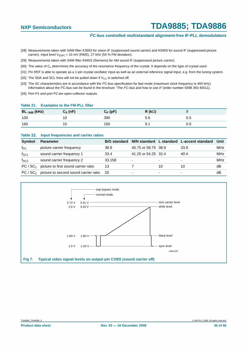
NXP Semiconductors TDA9885; TDA9886I2C-bus controlled multistandard alignment-free IF-PLL demodulators
[28] Measurements taken with SAW filter K3953 for vision IF (suppressed sound carrier) and K9453 for sound IF (suppressed picturecarrier). Input level Vi(SIF) = 10 mV (RMS), 27 kHz (54 % FM deviation).
[29] Measurements taken with SAW filter K9453 (Siemens) for AM sound IF (suppressed picture carrier).
[30] The value of Cx determines the accuracy of the resonance frequency of the crystal. It depends on the type of crystal used.
[31] Pin REF is able to operate as a 1-pin crystal oscillator input as well as an external reference signal input, e.g. from the tuning system.
[32] The SDA and SCL lines will not be pulled down if VCC is switched off.
[33] The AC characteristics are in accordance with the I2C-bus specification for fast mode (maximum clock frequency is 400 kHz).Information about the I2C-bus can be found in the brochure “The I2C-bus and how to use it” (order number 9398 393 40011).
[34] Port P1 and port P2 are open-collector outputs.
Table 21. Examples to the FM-PLL filter
BL−3dB (kHz) CS (nF) CP (pF) R (kΩ) ϑ
100 10 390 5.6 0.5
160 10 150 9.1 0.5
Table 22. Input frequencies and carrier ratios
Symbol Parameter B/G standard M/N standard L standard L-accent standard Unit
fPC picture carrier frequency 38.9 45.75 or 58.75 38.9 33.9 MHz
fSC1 sound carrier frequency 1 33.4 41.25 or 54.25 32.4 40.4 MHz
fSC2 sound carrier frequency 2 33.158 - - - MHz
PC / SC1 picture to first sound carrier ratio 13 7 10 10 dB
PC / SC2 picture to second sound carrier ratio 20 - - - dB
Fig 7. Typical video signal levels on output pin CVBS (sound carrier off)
1.20 V
1.80 V
3.20 V white level3.41 V
1.5 V
2.72 V2.6 V
1.83 V
zero carrier level
black level
sync level
mhc115
trap bypass mode
normal mode
TDA9885_TDA9886_3 © NXP B.V. 2008. All rights reserved.
Product data sheet Rev. 03 — 16 December 2008 35 of 56

NXP Semiconductors TDA9885; TDA9886I2C-bus controlled multistandard alignment-free IF-PLL demodulators
Fig 8. Ripple rejection condition
(1) VVAGC is VIF-AGC voltage and can only be measured at pin OP2 controlled by the I2C-bus(see Table 14).
(2) ITAGC is tuner current in TV mode with RTOP = 22 kΩ or setting via I2C-bus at −15 dB.
(3) ITAGC is tuner current in TV mode with RTOP = 10 kΩ or setting via I2C-bus at 0 dB.
(4) ITAGC is tuner current in TV mode with RTOP = 0 kΩ or setting via I2C-bus at +15 dB.
Fig 9. Typical VIF and tuner AGC characteristic
TDA9885TDA9886
VP = 5 V
VP(V)
t (s)
5 100 mV
fripple = 70 Hz
mhc114
mhc116
Vi(VIF) (dBµV)
VVAGC
(V)
ITAGC
(µA)
4
2
30 40 50 601
70 80 90 100 110
3
0
100
200
300
400
500
600
120
(4)(2) (3)(1)
TDA9885_TDA9886_3 © NXP B.V. 2008. All rights reserved.
Product data sheet Rev. 03 — 16 December 2008 36 of 56

NXP Semiconductors TDA9885; TDA9886I2C-bus controlled multistandard alignment-free IF-PLL demodulators
Fig 10. Typical tuner takeover point as a function of resistor R TOP
(1) FM mode.
(2) AM mode.
Fig 11. Typical SIF-AGC characteristic
0 24
110
60
70
100
90
80
mhb159
128 204 16
Vi(VIF)
(dBµV)
RTOP (kΩ)
VSAGC(V)
30 9050 110 130Vi(SIF) (dBµV)
70
5
4
2
1
3
mhc117
(2)
(1)
TDA9885_TDA9886_3 © NXP B.V. 2008. All rights reserved.
Product data sheet Rev. 03 — 16 December 2008 37 of 56
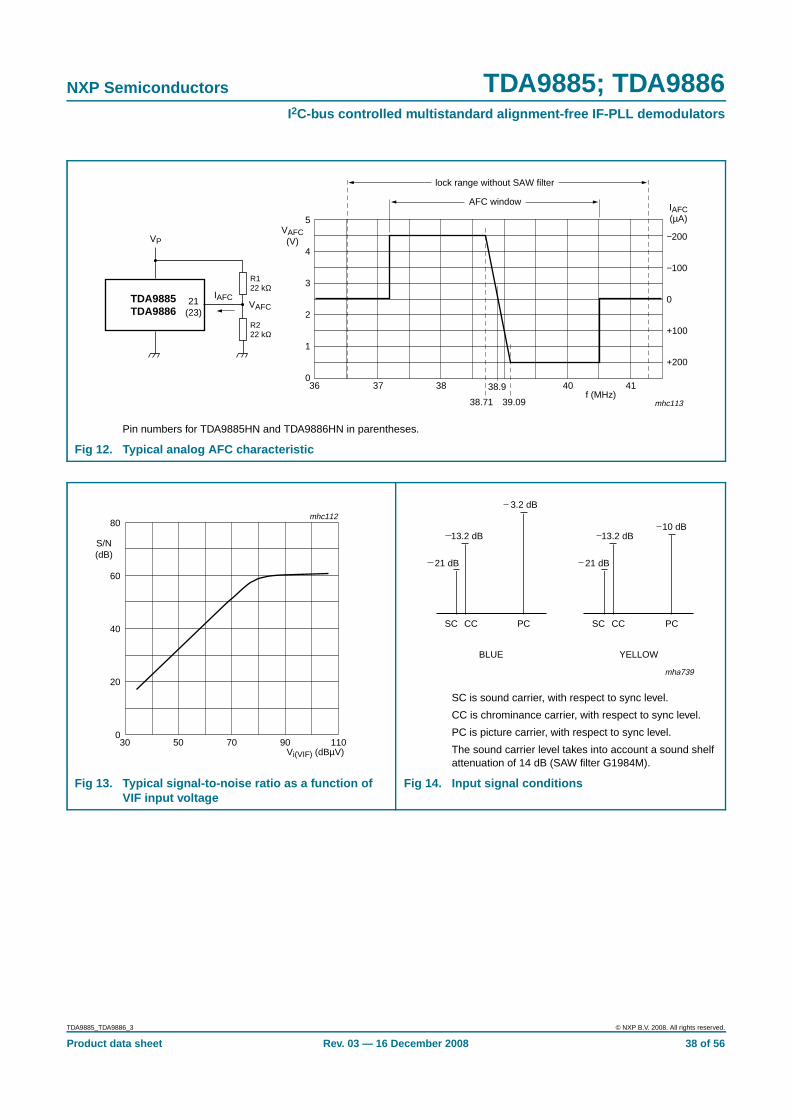
NXP Semiconductors TDA9885; TDA9886I2C-bus controlled multistandard alignment-free IF-PLL demodulators
Pin numbers for TDA9885HN and TDA9886HN in parentheses.
Fig 12. Typical analog AFC characteristic
mhc113
0
5
4
3
2
1
36 37 38 40 4138.9
38.71 39.09
lock range without SAW filter
f (MHz)
AFC window
VAFC(V)
+200
+100
0
−100
IAFC(µA)
−200
TDA9885TDA9886
21(23)
R122 kΩ
R222 kΩ
VP
VAFCIAFC
SC is sound carrier, with respect to sync level.
CC is chrominance carrier, with respect to sync level.
PC is picture carrier, with respect to sync level.
The sound carrier level takes into account a sound shelfattenuation of 14 dB (SAW filter G1984M).
Fig 13. Typical signal-to-noise ratio as a function ofVIF input voltage
Fig 14. Input signal conditions
030 50 110
80
60
20
40
mhc112
70 90Vi(VIF) (dBµV)
S/N(dB)
SC CC PC SC CC PC
BLUE YELLOW
21 dB
13.2 dB
3.2 dB
21 dB
13.2 dB10 dB
mha739
TDA9885_TDA9886_3 © NXP B.V. 2008. All rights reserved.
Product data sheet Rev. 03 — 16 December 2008 38 of 56

NXP Semiconductors TDA9885; TDA9886I2C-bus controlled multistandard alignment-free IF-PLL demodulators
Fig 15. Typical amplitude response for sound trap at M/N standard (including Korea)
mhc122
−402 2.5 3 3.5 4 4.5 5
−30
−20
−10
0
10
f (MHz)
H(s)(dB)
minimumrequirements
Overall delay is not shown, here the maximum ripple is specified.
Fig 16. Typical group delay for sound trap at M/N standard
mhb167
−1000 0.5 1.5 2 31 2.5 3.5 4
0
100
200
300
400
f (MHz)
groupdelay(ns)
ideal characteristicdue to pre-correction
in the transmitter
minimumrequirements
TDA9885_TDA9886_3 © NXP B.V. 2008. All rights reserved.
Product data sheet Rev. 03 — 16 December 2008 39 of 56

NXP Semiconductors TDA9885; TDA9886I2C-bus controlled multistandard alignment-free IF-PLL demodulators
Fig 17. Typical amplitude response for sound trap at B/G standard
mhb168
−404 4.5 5 5.5 6 6.5 7
−30
−20
−10
0
10
f (MHz)
H(s)(dB)
minimumrequirements
Overall delay is not shown, here the maximum ripple is specified.
Fig 18. Typical group delay for sound trap at B/G standard
mhb169
−1000 0.5 1.5 2 31 2.5 3.5 4 4.5 5
0
100
200
300
400
f (MHz)
groupdelay(ns)
ideal characteristicdue to pre-correction
in the transmitter
minimumrequirements
TDA9885_TDA9886_3 © NXP B.V. 2008. All rights reserved.
Product data sheet Rev. 03 — 16 December 2008 40 of 56

NXP Semiconductors TDA9885; TDA9886I2C-bus controlled multistandard alignment-free IF-PLL demodulators
Fig 19. Typical amplitude response for sound trap at I standard
Fig 20. Typical amplitude response for sound trap at D/K standard
mhc123
−404 4.5 5 5.5 6 6.5 7
−30
−20
−10
0
10
f (MHz)
H(s)(dB)
minimumrequirements
mhb171
−404 4.5 5 5.5 6 6.5 7
−30
−20
−10
0
10
f (MHz)
H(s)(dB)
minimumrequirements
TDA9885_TDA9886_3 © NXP B.V. 2008. All rights reserved.
Product data sheet Rev. 03 — 16 December 2008 41 of 56

NXP Semiconductors TDA9885; TDA9886I2C-bus controlled multistandard alignment-free IF-PLL demodulators
Conditions: PC / SC ratio measured at pins VIF1 and VIF2; via transformer; 27 kHz FM deviation; 50 µs de-emphasis.
(1) Signal.
(2) Noise at H-picture (“ITU-R BS.468-4” weighted quasi peak).
(3) Noise at black picture (“ITU-R BS.468-4” weighted quasi peak).
Fig 21. Audio signal-to-noise ratio as a function of picture-to-sound carrier ratio in intercarrier mode
4
10
0
−704952 46 43 40 1337 10 728 2225 193134 16
mhc118
−50
−30
−20
−10
−40
−60
S/NW
(dB)
(1)
(2)
(3)
gain controlled operation of FM-PLL
PC/SC ratio
Condition: m = 54 %.
(1) Signal.
(2) Noise.
Fig 22. Typical audio signal-to-noise ratio as a function of input signal at AM standard
Vi (dBµV)30 40 1109050 70 10060 80
mhc119
−30
−50
−10
10
S/NW(dB)
−70
−40
−60
−20
0(1)
(2)
TDA9885_TDA9886_3 © NXP B.V. 2008. All rights reserved.
Product data sheet Rev. 03 — 16 December 2008 42 of 56

NXP Semiconductors TDA9885; TDA9886I2C-bus controlled multistandard alignment-free IF-PLL demodulators
CAGC = 2.2 µF; m = 54 %.
Fig 23. Typical total harmonic distortion as a function of audio frequency at AM standard
mhc120
fAF (kHz)10−2 1021010−1 1
0.5
1.0
1.5
THD(%)
0
TDA9885_TDA9886_3 © NXP B.V. 2008. All rights reserved.
Product data sheet Rev. 03 — 16 December 2008 43 of 56
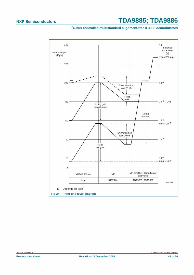
NXP Semiconductors TDA9885; TDA9886I2C-bus controlled multistandard alignment-free IF-PLL demodulators
(1) Depends on TOP.
Fig 24. Front-end level diagram
video 2 V (p-p)
0.66 × 10⁻³
0.66 × 10⁻⁵
mhc121
20
40
60
80
100
antenna input(dBµV)
120
140
10
VHF/UHF tuner VIF VIF amplifier, demodulatorand video
tuner SAW filter TDA9885, TDA9886
IF signalsRMS value
(V)
10−1
10−2 (TOP)
10−3
10−4
10−5
1
10
(1)
SAW insertionloss 20 dB
SAW insertionloss 20 dB
tuning gaincontrol range
40 dBRF gain
70 dBVIF AGC
IF slip6 dB
TDA9885_TDA9886_3 © NXP B.V. 2008. All rights reserved.
Product data sheet Rev. 03 — 16 December 2008 44 of 56
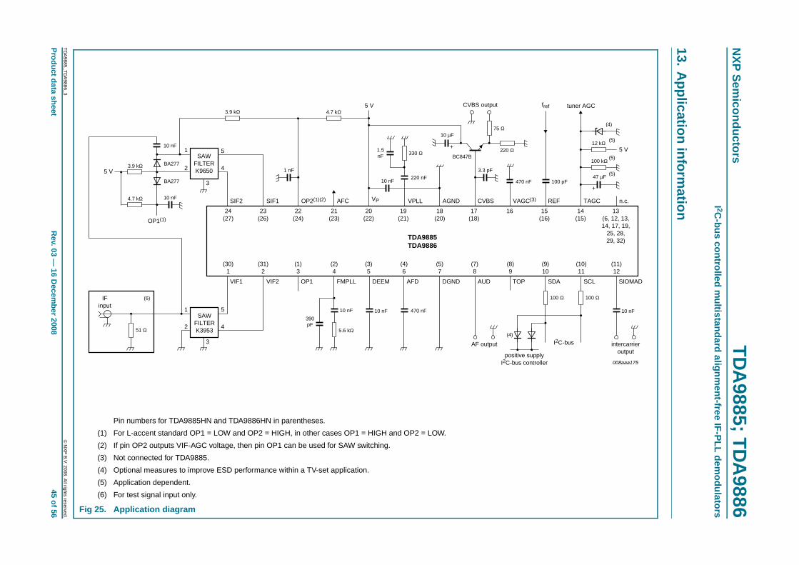
xxxx xxxxxxxxxxxxxxxxxxxxxxxxxxxxxx x xxxxxxxxxxxxxx xxxxxxxxxx xxx xxxxxx xxxxxxxxxxxxxxxxxxxxxxx xxxxxxxxxxxxxxxxxxxxxxxxxxx xxxxxx xx xxxxxxxxxxxxxxxxxxxxxxxxxxxxx xxxxxxxxxxxxxxxxxxxxxx xxxxxxxxxxx xxxxxxx xxxxxxxxxxxxxxxxxxxxxxxxxxxxxxxxxxx xxxxxxxxxxxxxx xxxxxx xx xxxxxxxxxxxxxxxxxxxxxxxxxxxxxxxx xxxxxxxxxxxxxxxxxxxxxxxx xxxxxxxxxxxxxxxxxxxxxxxxxxxxxxxxxxxxxxxxxxxxxxxxxxxxx xxxxxxxxxxx xxxxx x x
TD
A9885_T
DA
9886_3
Product data shee
NX
P S
emiconducto
13.A
pplication in(4)
tuner AGCfref
12 kΩ (5)
t
10 µF
5 V CVBS output4.7 kΩ
75 Ω
3.9 kΩ
rsT
DA
9885; TD
A9886
I 2C-bus controlled m
ultistandard alignment-free IF
-PLL dem
odulators
formation
47 µF
I2C-bus
supplyntroller 008aaa175
(9)10
15(16)
14(15)
13(6, 12, 13,14, 17, 19,
25, 28,29, 32)
5 V
(3)
(10)11
SCL
(11)12
SIOMADSDA
TAGC n.c.REF
100 kΩ
100 Ω 100 Ω
F 100 pF
intercarrieroutput
10 nF
(5)
(5)
© N
XP
B.V. 2008. A
ll rights reserved.
Rev. 03 —
16 Decem
ber 200845 of 56
Pin numbers for TDA9885HN and TDA9886HN in parentheses.
(1) For L-accent standard OP1 = LOW and OP2 = HIGH, in other cases OP1 = HIGH and OP2 = LOW.
(2) If pin OP2 outputs VIF-AGC voltage, then pin OP1 can be used for SAW switching.
(3) Not connected for TDA9885.
(4) Optional measures to improve ESD performance within a TV-set application.
(5) Application dependent.
(6) For test signal input only.
Fig 25. Application diagram
positive I2C-bus co
(30)1
(1)3
(5)7
(31)2
(2)4
(3)5
(4)6
22(24)
23(26)
18(20)
21(23)
20(22)
19(21)
(7)8
(8)9
17(18)
16
(4)
BA277
24(27)
470 nF
390pF
10 nF
VIF1 VIF2
SIF2 SIF1
OP1 FMPLL
VAGCAFC VPLLVP AGND
DEEM AFD DGND AUD TOP
1.5nF BC847B
CVBSOP2(1)(2)
5.6 kΩ
10 nF
220 Ω330 Ω
220 nF470 n10 nF
AF output
TDA9885TDA9886
51 Ω
1
2
5
4
3
IFinput
SAWFILTERK3953
1
2
5
4
3
SAWFILTERK9650 3.3 pF5 V
3.9 kΩ
4.7 kΩ
10 nF
(6)
1 nF
BA277
OP1(1)
10 nF

xxxx xxxxxxxxxxxxxxxxxxxxxxxxxxxxxx x xxxxxxxxxxxxxx xxxxxxxxxx xxx xxxxxx xxxxxxxxxxxxxxxxxxxxxxx xxxxxxxxxxxxxxxxxxxxxxxxxxx xxxxxx xx xxxxxxxxxxxxxxxxxxxxxxxxxxxxx xxxxxxxxxxxxxxxxxxxxxx xxxxxxxxxxx xxxxxxx xxxxxxxxxxxxxxxxxxxxxxxxxxxxxxxxxxx xxxxxxxxxxxxxx xxxxxx xx xxxxxxxxxxxxxxxxxxxxxxxxxxxxxxxx xxxxxxxxxxxxxxxxxxxxxxxx xxxxxxxxxxxxxxxxxxxxxxxxxxxxxxxxxxxxxxxxxxxxxxxxxxxxx xxxxxxxxxxx xxxxx x x
TD
A9885_T
DA
9886_3
Product data shee
NX
P S
emiconducto
14.Test inform
atle
4 MHz
tuner AGCoutput
t externareferenc
AFCoutput
VIF-PLLfilter (2)VP
100nF
1001.5nF
CVBSoutput
22kΩ 150 Ω
1 : 1SIF
input
rsT
DA
9885; TD
A9886
I 2C-bus controlled m
ultistandard alignment-free IF
-PLL dem
odulators
ion
rmer).
mhc124
(9)10
1516)
14(15)
13(6, 12, 13,14, 17, 19,
25, 28,29, 32)
(10)11
SCL
(11)12
SIOMADSDA
TAGC n.c.REF
Cx
R12.2kΩ(1)
MADselect
intercarrieroutput
© N
XP
B.V. 2008. A
ll rights reserved.
Rev. 03 —
16 Decem
ber 200846 of 56
Pin numbers for TDA9885HN and TDA9886HN in parentheses.
(1) Optional for I2C-bus address selection; see Table 23.
(2) Different VIF loop filter in comparison with the application diagram due to different input characteristics (SAW filter or transfo
(3) Not connected for TDA9885.
Fig 26. Test circuit
(30)1
(1)3
(5)7
(31)2
(2)4
(3)5
(4)6
22(24)
23(26)
18(20)
21(23)
20(22)
19(21)
(7)8
(8)9
17(18)
16(
24(27)
470 nF390pF
10 nF
VIF1 VIF2
SIF2 SIF1
OP1 FMPLL
VAGC(3)AFC VPLLVP AGND
DEEM AFD DGND AUD TOP
pF
CVBSOP2
5.6 kΩ
10 nF
FM-PLLfilter
22 kΩ150 kΩ150 kΩ
R2(1)R3
220 nF 470 nF
audiooutput
TDA9885TDA9886
51 Ω
1 : 1VIF
input
51 Ω
22 kΩ

NXP Semiconductors TDA9885; TDA9886I2C-bus controlled multistandard alignment-free IF-PLL demodulators
Table 23. I2C-bus address selectionS = R/W selection bit.
Option R1 not used R1 = 2.2 kΩ
R2 and R3 not used 1000 011S 1000 010S
R2 = R3 = 150 kΩ 1001 011S 1001 010S
TDA9885_TDA9886_3 © NXP B.V. 2008. All rights reserved.
Product data sheet Rev. 03 — 16 December 2008 47 of 56
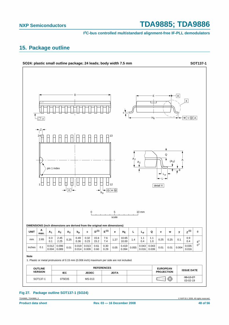
NXP Semiconductors TDA9885; TDA9886I2C-bus controlled multistandard alignment-free IF-PLL demodulators
15. Package outline
Fig 27. Package outline SOT137-1 (SO24)
UNITA
max. A1 A2 A3 bp c D (1) E (1) (1)e HE L L p Q Zywv θ
REFERENCESOUTLINEVERSION
EUROPEANPROJECTION ISSUE DATE
IEC JEDEC JEITA
mm
inches
2.65 0.30.1
2.452.25
0.490.36
0.320.23
15.615.2
7.67.4
1.2710.6510.00
1.11.0
0.90.4 8
0
o
o
0.25 0.1
DIMENSIONS (inch dimensions are derived from the original mm dimensions)
Note
1. Plastic or metal protrusions of 0.15 mm (0.006 inch) maximum per side are not included.
1.10.4
SOT137-1
X
12
24
w M
θ
AA1
A2
bp
D
HE
Lp
Q
detail X
E
Z
c
L
v M A
13
(A )3
A
y
0.25
075E05 MS-013
pin 1 index
0.1 0.0120.004
0.0960.089
0.0190.014
0.0130.009
0.610.60
0.300.29
0.05
1.4
0.0550.4190.394
0.0430.039
0.0350.016
0.01
0.25
0.01 0.0040.0430.016
0.01
e
1
0 5 10 mm
scale
SO24: plastic small outline package; 24 leads; body width 7.5 mm SOT137-1
99-12-2703-02-19
TDA9885_TDA9886_3 © NXP B.V. 2008. All rights reserved.
Product data sheet Rev. 03 — 16 December 2008 48 of 56
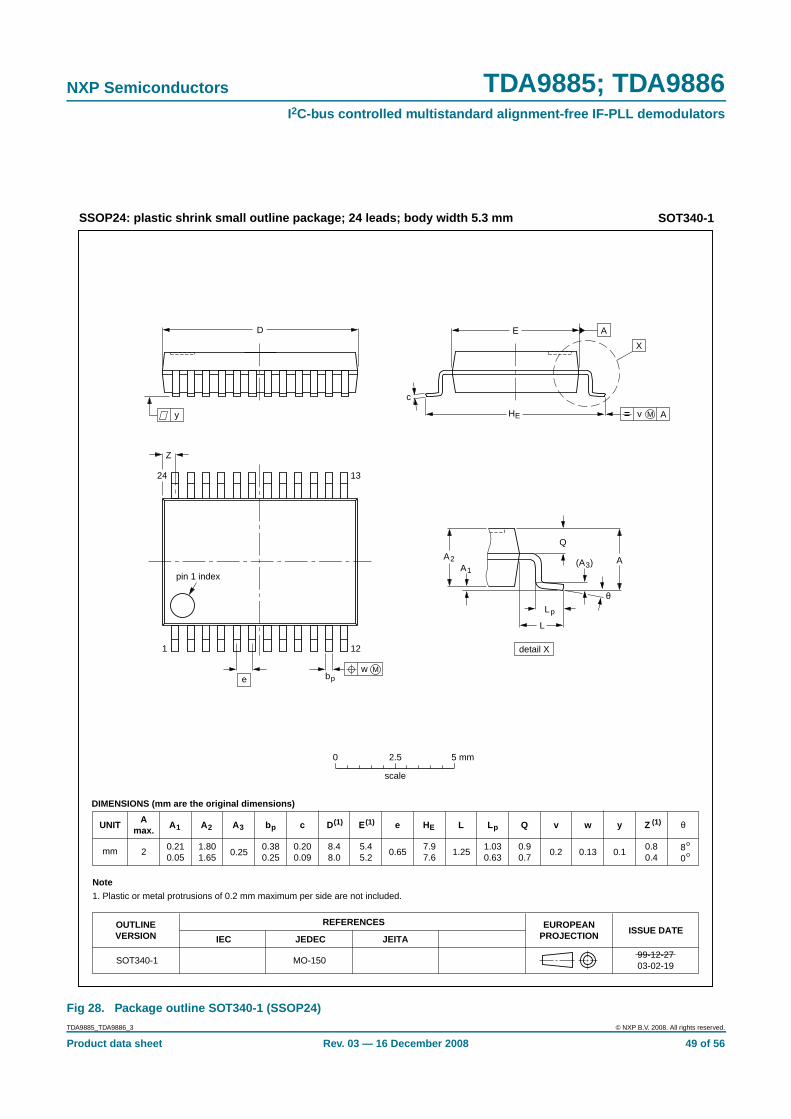
NXP Semiconductors TDA9885; TDA9886I2C-bus controlled multistandard alignment-free IF-PLL demodulators
Fig 28. Package outline SOT340-1 (SSOP24)
UNIT A1 A2 A3 bp c D(1) E(1) (1)e HE L L p Q Zywv θ
REFERENCESOUTLINEVERSION
EUROPEANPROJECTION ISSUE DATE
IEC JEDEC JEITA
mm 0.210.05
1.801.65
0.380.25
0.200.09
8.48.0
5.45.2
0.65 1.257.97.6
0.90.7
0.80.4
80
o
o0.13 0.10.2
DIMENSIONS (mm are the original dimensions)
Note
1. Plastic or metal protrusions of 0.2 mm maximum per side are not included.
1.030.63
SOT340-1 MO-15099-12-2703-02-19
X
w M
θ
AA1
A2
bp
D
HE
Lp
Q
detail X
E
Z
e
c
L
v M A
(A )3
A
1 12
24 13
0.25
y
pin 1 index
0 2.5 5 mm
scale
SSOP24: plastic shrink small outline package; 24 leads; body width 5.3 mm SOT340-1
Amax.
2
TDA9885_TDA9886_3 © NXP B.V. 2008. All rights reserved.
Product data sheet Rev. 03 — 16 December 2008 49 of 56
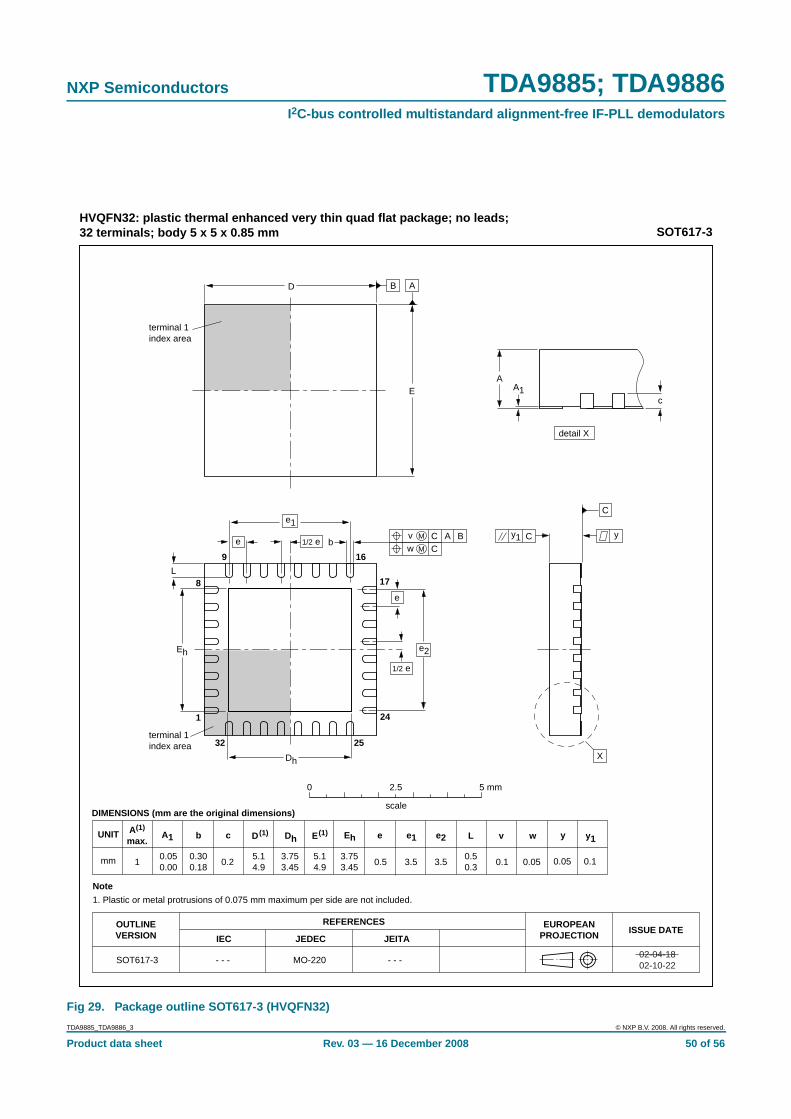
NXP Semiconductors TDA9885; TDA9886I2C-bus controlled multistandard alignment-free IF-PLL demodulators
Fig 29. Package outline SOT617-3 (HVQFN32)
terminal 1index area
0.51
A1 EhbUNIT ye
0.2
c
REFERENCESOUTLINEVERSION
EUROPEANPROJECTION ISSUE DATE
IEC JEDEC JEITA
mm 5.14.9
Dh
3.753.45
y1
5.14.9
3.753.45
e1
3.5
e2
3.50.300.18
0.050.00
0.05 0.1
DIMENSIONS (mm are the original dimensions)
SOT617-3 MO-220- - - - - -
0.50.3
L
0.1
v
0.05
w
0 2.5 5 mm
scale
SOT617-3HVQFN32: plastic thermal enhanced very thin quad flat package; no leads;32 terminals; body 5 x 5 x 0.85 mm
A(1)
max.
AA1
c
detail X
yy1 Ce
L
Eh
Dh
e
e1
b
9 16
32 25
24
178
1
X
D
E
C
B A
e2
terminal 1index area
02-04-1802-10-22
1/2 e
1/2 eAC
CBv M
w M
E(1)
Note
1. Plastic or metal protrusions of 0.075 mm maximum per side are not included.
D(1)
TDA9885_TDA9886_3 © NXP B.V. 2008. All rights reserved.
Product data sheet Rev. 03 — 16 December 2008 50 of 56

NXP Semiconductors TDA9885; TDA9886I2C-bus controlled multistandard alignment-free IF-PLL demodulators
16. Soldering of SMD packages
This text provides a very brief insight into a complex technology. A more in-depth accountof soldering ICs can be found in Application Note AN10365 “Surface mount reflowsoldering description”.
16.1 Introduction to solderingSoldering is one of the most common methods through which packages are attached toPrinted Circuit Boards (PCBs), to form electrical circuits. The soldered joint provides boththe mechanical and the electrical connection. There is no single soldering method that isideal for all IC packages. Wave soldering is often preferred when through-hole andSurface Mount Devices (SMDs) are mixed on one printed wiring board; however, it is notsuitable for fine pitch SMDs. Reflow soldering is ideal for the small pitches and highdensities that come with increased miniaturization.
16.2 Wave and reflow solderingWave soldering is a joining technology in which the joints are made by solder coming froma standing wave of liquid solder. The wave soldering process is suitable for the following:
• Through-hole components
• Leaded or leadless SMDs, which are glued to the surface of the printed circuit board
Not all SMDs can be wave soldered. Packages with solder balls, and some leadlesspackages which have solder lands underneath the body, cannot be wave soldered. Also,leaded SMDs with leads having a pitch smaller than ~0.6 mm cannot be wave soldered,due to an increased probability of bridging.
The reflow soldering process involves applying solder paste to a board, followed bycomponent placement and exposure to a temperature profile. Leaded packages,packages with solder balls, and leadless packages are all reflow solderable.
Key characteristics in both wave and reflow soldering are:
• Board specifications, including the board finish, solder masks and vias
• Package footprints, including solder thieves and orientation
• The moisture sensitivity level of the packages
• Package placement
• Inspection and repair
• Lead-free soldering versus SnPb soldering
16.3 Wave solderingKey characteristics in wave soldering are:
• Process issues, such as application of adhesive and flux, clinching of leads, boardtransport, the solder wave parameters, and the time during which components areexposed to the wave
• Solder bath specifications, including temperature and impurities
TDA9885_TDA9886_3 © NXP B.V. 2008. All rights reserved.
Product data sheet Rev. 03 — 16 December 2008 51 of 56

NXP Semiconductors TDA9885; TDA9886I2C-bus controlled multistandard alignment-free IF-PLL demodulators
16.4 Reflow solderingKey characteristics in reflow soldering are:
• Lead-free versus SnPb soldering; note that a lead-free reflow process usually leads tohigher minimum peak temperatures (see Figure 30) than a SnPb process, thusreducing the process window
• Solder paste printing issues including smearing, release, and adjusting the processwindow for a mix of large and small components on one board
• Reflow temperature profile; this profile includes preheat, reflow (in which the board isheated to the peak temperature) and cooling down. It is imperative that the peaktemperature is high enough for the solder to make reliable solder joints (a solder pastecharacteristic). In addition, the peak temperature must be low enough that thepackages and/or boards are not damaged. The peak temperature of the packagedepends on package thickness and volume and is classified in accordance withTable 24 and 25
Moisture sensitivity precautions, as indicated on the packing, must be respected at alltimes.
Studies have shown that small packages reach higher temperatures during reflowsoldering, see Figure 30.
Table 24. SnPb eutectic process (from J-STD-020C)
Package thickness (mm) Package reflow temperature ( °C)
Volume (mm 3)
< 350 ≥ 350
< 2.5 235 220
≥ 2.5 220 220
Table 25. Lead-free process (from J-STD-020C)
Package thickness (mm) Package reflow temperature ( °C)
Volume (mm 3)
< 350 350 to 2000 > 2000
< 1.6 260 260 260
1.6 to 2.5 260 250 245
> 2.5 250 245 245
TDA9885_TDA9886_3 © NXP B.V. 2008. All rights reserved.
Product data sheet Rev. 03 — 16 December 2008 52 of 56
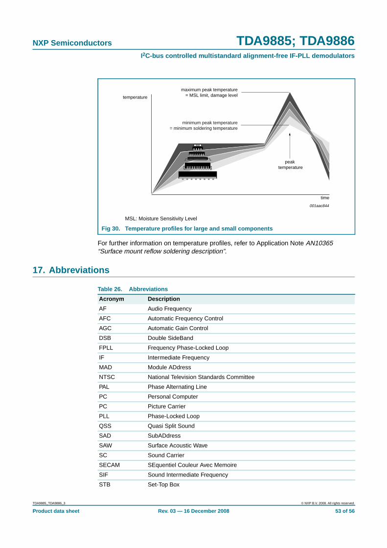
NXP Semiconductors TDA9885; TDA9886I2C-bus controlled multistandard alignment-free IF-PLL demodulators
For further information on temperature profiles, refer to Application Note AN10365“Surface mount reflow soldering description”.
17. Abbreviations
MSL: Moisture Sensitivity Level
Fig 30. Temperature profiles for large and small components
001aac844
temperature
time
minimum peak temperature= minimum soldering temperature
maximum peak temperature= MSL limit, damage level
peak temperature
Table 26. Abbreviations
Acronym Description
AF Audio Frequency
AFC Automatic Frequency Control
AGC Automatic Gain Control
DSB Double SideBand
FPLL Frequency Phase-Locked Loop
IF Intermediate Frequency
MAD Module ADdress
NTSC National Television Standards Committee
PAL Phase Alternating Line
PC Personal Computer
PC Picture Carrier
PLL Phase-Locked Loop
QSS Quasi Split Sound
SAD SubADdress
SAW Surface Acoustic Wave
SC Sound Carrier
SECAM SEquentiel Couleur Avec Memoire
SIF Sound Intermediate Frequency
STB Set-Top Box
TDA9885_TDA9886_3 © NXP B.V. 2008. All rights reserved.
Product data sheet Rev. 03 — 16 December 2008 53 of 56

NXP Semiconductors TDA9885; TDA9886I2C-bus controlled multistandard alignment-free IF-PLL demodulators
18. Revision history
TOP TakeOver Point
VCO Voltage-Controlled Oscillator
VIF Vision Intermediate Frequency
VITS Vertical Interval Test Signal
VTR Video Tape Recorder
Table 26. Abbreviations …continued
Acronym Description
Table 27. Revision history
Document ID Release date Data sheet status Change notice Supersedes
TDA9885_TDA9886_3 20081216 Product data sheet - TDA9885_TDA9886_2
Modifications: • The format of this data sheet has been redesigned to comply with the new identityguidelines of NXP Semiconductors.
• Legal texts have been adapted to the new company name where appropriate.
• Section 5: added V5 versions
• Figure 25; update on application diagram
TDA9885_TDA9886_2 20031002 Product specification - TDA9885_TDA9886_1
TDA9885_TDA9886_1 20020305 Product specification - -
TDA9885_TDA9886_3 © NXP B.V. 2008. All rights reserved.
Product data sheet Rev. 03 — 16 December 2008 54 of 56

NXP Semiconductors TDA9885; TDA9886I2C-bus controlled multistandard alignment-free IF-PLL demodulators
19. Legal information
19.1 Data sheet status
[1] Please consult the most recently issued document before initiating or completing a design.
[2] The term ‘short data sheet’ is explained in section “Definitions”.
[3] The product status of device(s) described in this document may have changed since this document was published and may differ in case of multiple devices. The latest product statusinformation is available on the Internet at URL http://www.nxp.com.
19.2 Definitions
Draft — The document is a draft version only. The content is still underinternal review and subject to formal approval, which may result inmodifications or additions. NXP Semiconductors does not give anyrepresentations or warranties as to the accuracy or completeness ofinformation included herein and shall have no liability for the consequences ofuse of such information.
Short data sheet — A short data sheet is an extract from a full data sheetwith the same product type number(s) and title. A short data sheet is intendedfor quick reference only and should not be relied upon to contain detailed andfull information. For detailed and full information see the relevant full datasheet, which is available on request via the local NXP Semiconductors salesoffice. In case of any inconsistency or conflict with the short data sheet, thefull data sheet shall prevail.
19.3 Disclaimers
General — Information in this document is believed to be accurate andreliable. However, NXP Semiconductors does not give any representations orwarranties, expressed or implied, as to the accuracy or completeness of suchinformation and shall have no liability for the consequences of use of suchinformation.
Right to make changes — NXP Semiconductors reserves the right to makechanges to information published in this document, including withoutlimitation specifications and product descriptions, at any time and withoutnotice. This document supersedes and replaces all information supplied priorto the publication hereof.
Suitability for use — NXP Semiconductors products are not designed,authorized or warranted to be suitable for use in medical, military, aircraft,space or life support equipment, nor in applications where failure ormalfunction of an NXP Semiconductors product can reasonably be expectedto result in personal injury, death or severe property or environmental
damage. NXP Semiconductors accepts no liability for inclusion and/or use ofNXP Semiconductors products in such equipment or applications andtherefore such inclusion and/or use is at the customer’s own risk.
Applications — Applications that are described herein for any of theseproducts are for illustrative purposes only. NXP Semiconductors makes norepresentation or warranty that such applications will be suitable for thespecified use without further testing or modification.
Limiting values — Stress above one or more limiting values (as defined inthe Absolute Maximum Ratings System of IEC 60134) may cause permanentdamage to the device. Limiting values are stress ratings only and operation ofthe device at these or any other conditions above those given in theCharacteristics sections of this document is not implied. Exposure to limitingvalues for extended periods may affect device reliability.
Terms and conditions of sale — NXP Semiconductors products are soldsubject to the general terms and conditions of commercial sale, as publishedat http://www.nxp.com/profile/terms, including those pertaining to warranty,intellectual property rights infringement and limitation of liability, unlessexplicitly otherwise agreed to in writing by NXP Semiconductors. In case ofany inconsistency or conflict between information in this document and suchterms and conditions, the latter will prevail.
No offer to sell or license — Nothing in this document may be interpretedor construed as an offer to sell products that is open for acceptance or thegrant, conveyance or implication of any license under any copyrights, patentsor other industrial or intellectual property rights.
Quick reference data — The Quick reference data is an extract of theproduct data given in the Limiting values and Characteristics sections of thisdocument, and as such is not complete, exhaustive or legally binding.
19.4 TrademarksNotice: All referenced brands, product names, service names and trademarksare the property of their respective owners.
I2C-bus — logo is a trademark of NXP B.V.
20. Contact information
For more information, please visit: http://www .nxp.com
For sales office addresses, please send an email to: salesad [email protected]
Document status [1] [2] Product status [3] Definition
Objective [short] data sheet Development This document contains data from the objective specification for product development.
Preliminary [short] data sheet Qualification This document contains data from the preliminary specification.
Product [short] data sheet Production This document contains the product specification.
TDA9885_TDA9886_3 © NXP B.V. 2008. All rights reserved.
Product data sheet Rev. 03 — 16 December 2008 55 of 56
NXP Semiconductors TDA9885; TDA9886I2C-bus controlled multistandard alignment-free IF-PLL demodulators
21. Contents
1 General description . . . . . . . . . . . . . . . . . . . . . . 12 Features . . . . . . . . . . . . . . . . . . . . . . . . . . . . . . . 13 Applications . . . . . . . . . . . . . . . . . . . . . . . . . . . . 24 Quick reference data . . . . . . . . . . . . . . . . . . . . . 25 Ordering information . . . . . . . . . . . . . . . . . . . . . 46 Block diagram . . . . . . . . . . . . . . . . . . . . . . . . . . 57 Pinning information . . . . . . . . . . . . . . . . . . . . . . 67.1 Pinning . . . . . . . . . . . . . . . . . . . . . . . . . . . . . . . 67.2 Pin description . . . . . . . . . . . . . . . . . . . . . . . . . 78 Functional description . . . . . . . . . . . . . . . . . . . 88.1 VIF amplifier . . . . . . . . . . . . . . . . . . . . . . . . . . . 88.2 Tuner AGC and VIF AGC . . . . . . . . . . . . . . . . . 88.3 VIF-AGC detector . . . . . . . . . . . . . . . . . . . . . . . 98.4 FPLL detector . . . . . . . . . . . . . . . . . . . . . . . . . . 98.5 VCO and divider . . . . . . . . . . . . . . . . . . . . . . . . 98.6 AFC and digital acquisition help . . . . . . . . . . . 108.7 Video demodulator and amplifier . . . . . . . . . . 108.8 Sound carrier trap . . . . . . . . . . . . . . . . . . . . . . 118.9 SIF amplifier . . . . . . . . . . . . . . . . . . . . . . . . . . 118.10 SIF-AGC detector . . . . . . . . . . . . . . . . . . . . . . 118.11 Single reference QSS mixer . . . . . . . . . . . . . . 118.12 AM demodulator . . . . . . . . . . . . . . . . . . . . . . . 128.13 FM demodulator and acquisition help. . . . . . . 128.14 Audio amplifier and mute time constant . . . . . 128.15 Internal voltage stabilizer . . . . . . . . . . . . . . . . 138.16 I2C-bus transceiver and MAD . . . . . . . . . . . . . 139 I2C-bus control . . . . . . . . . . . . . . . . . . . . . . . . . 149.1 Read format . . . . . . . . . . . . . . . . . . . . . . . . . . 149.1.1 Slave address . . . . . . . . . . . . . . . . . . . . . . . . . 149.1.2 Data byte . . . . . . . . . . . . . . . . . . . . . . . . . . . . 159.2 Write format . . . . . . . . . . . . . . . . . . . . . . . . . . 169.2.1 Subaddress (A data). . . . . . . . . . . . . . . . . . . . 179.2.2 Data byte for switching mode (B data) . . . . . . 179.2.3 Data byte for adjust mode (C data). . . . . . . . . 189.2.4 Data byte for data mode (E data) . . . . . . . . . . 1910 Limiting values. . . . . . . . . . . . . . . . . . . . . . . . . 2111 Thermal characteristics. . . . . . . . . . . . . . . . . . 2112 Characteristics . . . . . . . . . . . . . . . . . . . . . . . . . 2213 Application information. . . . . . . . . . . . . . . . . . 4514 Test information . . . . . . . . . . . . . . . . . . . . . . . . 4615 Package outline . . . . . . . . . . . . . . . . . . . . . . . . 4816 Soldering of SMD packages . . . . . . . . . . . . . . 5116.1 Introduction to soldering . . . . . . . . . . . . . . . . . 5116.2 Wave and reflow soldering . . . . . . . . . . . . . . . 5116.3 Wave soldering . . . . . . . . . . . . . . . . . . . . . . . . 51
16.4 Reflow soldering. . . . . . . . . . . . . . . . . . . . . . . 5217 Abbreviations . . . . . . . . . . . . . . . . . . . . . . . . . 5318 Revision history . . . . . . . . . . . . . . . . . . . . . . . 5419 Legal information . . . . . . . . . . . . . . . . . . . . . . 5519.1 Data sheet status . . . . . . . . . . . . . . . . . . . . . . 5519.2 Definitions . . . . . . . . . . . . . . . . . . . . . . . . . . . 5519.3 Disclaimers. . . . . . . . . . . . . . . . . . . . . . . . . . . 5519.4 Trademarks . . . . . . . . . . . . . . . . . . . . . . . . . . 5520 Contact information . . . . . . . . . . . . . . . . . . . . 5521 Contents. . . . . . . . . . . . . . . . . . . . . . . . . . . . . . 56
© NXP B.V. 2008. All rights reserved.For more information, please visit: http://www.nxp.comFor sales office addresses, please send an email to: [email protected]
Date of release: 16 December 2008
Document identifier: TDA9885_TDA9886_3
Please be aware that important notices concerning this document and the product(s)described herein, have been included in section ‘Legal information’.