synthesis of a fully-integrated digital signal source for
TRANSCRIPT

Synthesis of a Fully-Integrated Digital Signal Source for Communications from
Chaotic Dynamics-based Oscillations
by
Chance M. Glenn, Sr.
A dissertation submitted to Johns Hopkins University in conformity with the
requirements for the degree of Doctor of Philosophy
Baltimore, MD
January 2003
© Chance M. Glenn, Sr. 2003
All Rights Reserved

ABSTRACT
This work is the conceptualization, derivation, analysis, and fabrication of a fully
practical digital signal source designed from a chaotic oscillator. In it we show how a
simple electronic circuit based upon the Colpitts oscillator, can be made to produce
highly complex signals capable of carrying digital information. We show a direct
relationship between the continuous-time chaotic oscillations produced by the circuit and
the logistic map, which is discrete-time, one-dimensional map that is a fundamental
paradigm for the study of chaotic systems. We demonstrate the direct encoding of binary
information into the oscillations of the chaotic circuit. We demonstrate a new concept in
power amplification, called syncrodyne amplification, which uses fundamental properties
of chaotic oscillators to provide high-efficiency, high gain amplification of standard
communication waveforms as well as typical chaotic oscillations. We show modeling
results of this system providing nearly 60-dB power gain and 80% PAE for
communications waveforms conforming to GMSK modulation. Finally we show results
from a fabricated syncrodyne amplifier circuit operating at 2 MHz, providing over 40-dB
power gain and 72% PAE, and propose design criteria for an 824 -850 MHz circuit
utilizing heterojunction bipolar transistors (HBTs), providing the basis for microwave
frequency realization.

iii
Copyright, 2003, by Chance M. Glenn, Sr., All Rights Reserved.

iv
This thesis is dedicated to my wife Marsha. She has undoubtedly remained by my side
through every kind of weather. I would not have been able to do this without her. Even
during the writing of this dissertation your importance to me is demonstrated. Also, to
my God, and my Savior, Who gave my wife and my children, Michael, Markiss, Melyssa
and Morgen to me, and Who inspires creativity and perseverance in all of His children,
thank You.

v
ACKNOWLEDGMENTS
I would like to acknowledge my advisor, Dr. Charles R. Westgate, for the
consistent encouragement to push farther, the freedom to explore new ideas and the
persistency to never let me quit.
I would also like to acknowledge Dr. Scott T. Hayes, who first became my friend,
then became my mentor, then became my colleague, and finally became my business
partner. Our relationship has indeed been fruitful over these 16 years. We have plenty
more mountains to climb I’m certain. I could not have done this without his inspiration
to never settle for mundane ideas, to explore deeper than the average, and to pursue
scientific knowledge with vigor and integrity. He has helped to shape my character more
than he could ever know.
I would like to acknowledge Dr. Christian Fazi, who first put this hair-brained
idea in my head to pursue my Master’s and Doctoral degrees. He has remained a
constant source of encouragement through the ups and the downs. His contagious love
for new ideas is one of the reasons I was able to stay on this course.
I would finally like to acknowledge all of my immediate family: father and
mother Wallace and Shirley, my siblings: Wallace, who I grew up the closest to and gave
me my sense of drive and competitiveness, Victoria, Christopher, Patty, Robin, Carlton
and Cameron, who saw my love for tearing things apart to see how they worked, and
steered me down the road of electronics and engineering, and finally my grandmother
who raised me. I love you all.

vi
TABLE OF CONTENTS
Page
LIST OF TABLES............................................................................................................ vii
LIST OF FIGURES ......................................................................................................... viii
Chapter
1. Introduction..........................................................................................................1 1.1 Description of the Work .....................................................................1
1.2 Chaotic Dynamics ...............................................................................3 1.3 Applications of Chaotic Dynamics....................................................10 1.4 Communication and Chaotic Dynamics............................................10 1.5 Wireless Communications and the Opportunity................................12
2. A Paradigm Study: The Colpitts Oscillator .......................................................162.1 Rationale............................................................................................16
2.2 Properties and Measures....................................................................20 2.3 The Colpitts Oscillator as a Digital Signal Source............................23 2.4 Syncrodyne Amplification.................................................................28
2.5 Modeling Results and Analysis .........................................................31
3. Custom Chaotic Oscillator Design. ...................................................................413.1 Design Criteria...................................................................................41
3.2 PSPICE Modeling .............................................................................433.3 Circuit Fabrication and Testing .........................................................463.4 Preliminary Design of a 850 MHz Circuit ........................................53
4. Conclusion .........................................................................................................574.1 Discussion of Results ........................................................................57
4.2 Implications .......................................................................................59
APPENDIXESA. MATLAB Procedures for Modeling and Analysis ...........................................61B. SPICE Circuit Files ...........................................................................................79
LITERATURE CITED ......................................................................................................81
VITA..................................................................................................................................84

vii
LIST OF TABLES
Table Page
1.1. Demonstration of the spreading of initial conditions for the logistic map for ρ = 4(chaotic) ............................................................................................................................7
1.2. Mobile Handset Market: Mobile Subscriber Forecast (World), 1999 – 2005 ......12
1.3. Summary of performance parameters for the leading PA products......................13
2.1. Calculation of local Lynapunov exponents for the discrete time mapping of theColpitts oscillator. .................................................................................................22
2.2. Circuit parameter values used for syncrodyne amplifier model analysis .............31
viii
LIST OF FIGURES
Figure Page
1.1. Plots of the logistic map for ρ = 1,2,3 and 4.........................................................4
1.2. Bifurcation diagram for the logistic map as parameter ρ is varied.......................6
1.3. Two chaotic oscillators synchronized together. Oscillator B tracks the identicalbehavior of oscillator A ....................................................................................................9
1.4. Lorenz oscillations encoded to carry a digital sequence which produces the ASCIItext ‘c-h-a-o-s’ ..................................................................................................................11
1.5. A typical I-V characteristic curve for a transistor describing the linear and nonlinearregions of operation ..........................................................................................................14
2.1. A general voltage feedback system.......................................................................16
2.2. Transistor based Colpitts oscillator circuit used for this analysis.........................16
2.3. Collector voltage versus time for the Colpitts circuit using a parameter set thatproduces Rössler type chaos. ................................................................................18
2.4. Three-dimensional representation of the state-space trajectories for the Colpittsoscillator illustrating the Rössler band..................................................................18
2.5. Power spectrum of the collector voltage for the Colpitts oscillator in a chaoticmode of operation .................................................................................................19
2.6. Chaotic attractor for the Colpitts oscillator with an Poincaré surface of sectionerected in the flow.................................................................................................20
2.7. Poincaré map produced by the surface of section in figure 2.6 ............................21
2.8. Return map for the collector voltage as produced by sequential observation ofpoints generated by the Poincare mapping. Note its resemblance to the logisticmap........................................................................................................................21
2.9. The return map for the Colpitts chaotic oscillator illustrating the binary partitionand the generation of digital information..............................................................23
2.10. The Poincaré map of the Colpitts chaotic oscillation showing the placement of the

ix
binary partition boundary. Trajectories passing through the Poincaré surface ofsection on either side of the boundary produce bit 0 or 1.....................................24
2.11. 8-bit binary coding function for the Colpitts oscillator ........................................25
2.12. State-space trajectories encoded to produce the 8-bit binary sequence 01011101. ...............................................................................................................................26
2.13. Time-varying collector voltage demonstrating the 8-bit binary encoding 01011101embedded into the oscillations..............................................................................27
2.14. Block diagram of a Syncrodyne amplifier system................................................29
2.15. Circuit schematic diagram for a Colpitts oscillator based syncrodyne amplifier .30
2.16. (a) In-phase and (b) quadrature baseband components of a 2 MHz GSMwaveform along with (c) the modulated carrier and (d) the power spectrum.......34
2.17. Variation of the attractor volume as the capacitor C is changed ..........................35
2.18. Power gain as a function of the tuning capacitance C ..........................................36
2.19. Surface map illustrating the PAE for peak-to-peak input voltages and tuningcapacitance values.................................................................................................37
2.20. Relationship between the peak power gain and the peak sinusoidal input voltagefor the syncrodyne amplifier circuit......................................................................38
2.21. Overall PAE peak power gain relationship for the syncrodyne amplifier circuit.Note that there are regions of operation where the system is capable of nearly80% PAE and greater than 55 dB gain. ................................................................39
3.1. 2 MHz syncrodyne amplifier circuit schematic diagram......................................42
3.2. Two-dimensional projection of the chaotic attractor produced by the 2 MHzColpitts oscillator SPICE simulation ....................................................................44
3.3. Time-dependent oscillation of the emitter voltage in a slightly chaotic state.......44
3.4. Frequency spectrum of the emitter voltage oscillations illustrating the broadfrequency content indicative of chaotic behavior .................................................45
3.5. Photograph of the fabricated 2 MHz syncrodyne amplifier circuit ......................46
3.6. Picture of the PCB used to fabricate the 2 MHz syncrodyne amplifier circuit.....46
x
3.7. Measured time signal from the Colpitt’s oscillator circuit ...................................47
3.8. The Colpitts attractor controlled on a constrained set. The Cantor set structure is aresult of the constraint...........................................................................................48
3.9. Uncontrolled 2 MHz Colpitts attractor showing a two-dimensional projection ofthe state-space attractor.........................................................................................49
3.10. Symbolic dynamics controlled Colpitts attractor..................................................50
3.11. Results from the 2 MHz syncrodyne amplifier circuit showing (a) the inputsignal, (b) the output signal and (c) the error signal .............................................51
3.12 Comparison of experimental data from the 2 MHz syncrodyne amplifier withmodeling results ....................................................................................................52
3.13. DC I-V characteristics for the high-frequency HBT used to model the 850 MHzcircuit ....................................................................................................................53
3.14. Schematic diagram of the high-frequency, Colpitts type, chaotic oscillatormodeled using an HBT .........................................................................................54
3.15. Time dependent oscillation of the voltage vC1 for the 850 MHz chaotic oscillatorsimulation..............................................................................................................55
3.16. Two-dimensional projection of the state-space for the 850 MHz chaotic oscillatorsimulation..............................................................................................................56
3.17. Frequency spectrum for the voltage across C1 for the 850 MHz chaotic oscillatorsimulation..............................................................................................................56

1
CHAPTER 1
Introduction
1.1 Description of the Work
This work represents original concepts derived by the author and is intended to
demonstrate that the engineering implementation of chaotic oscillations in digital
communications systems can show clear performance enhancements as compared to
traditional designs. We intend to show this in two ways. First, we intend to show that it
is both possible and practical to encode arbitrary binary information into chaotic
oscillations. There has been a great deal of prior formalization and experimentation
surrounding the application of chaos to communications [1,2]. We show the benefits of
using the direct encoding method of controlling symbolic dynamics first proposed by
Hayes, et. al [3]. Second, we introduce formally and demonstrate experimentally, a new
method of high-gain, high-efficiency power amplification of standard communication
waveforms using a chaotic process. We show that this process, called syncrodyne
amplification, is capable of operating on communication waveforms such as GSM and
CDMA and capable of providing gains in excess of 60 dB and power added efficiencies
greater than 70%.
In a general sense, the goal of this work is to provide further evidence of the notion
that chaotic dynamics can be useful for technological applications. The paradigm shift
that occurred in the dynamics community when the implications of chaotic dynamics was
understood [4] has not been fully realized in applied engineering circles. A primary
reason for this has been the failure to present tangible performance advantages of chaotic
systems over traditional systems. Our goal is to provide solid examples of such

2
advantages.
3
1.2 Chaotic Dynamics
What is chaos? After over one hundred years of research, study, scrutiny,
analysis, modeling, and experimentation, this is a question that still eludes a definitive
answer. Chaos is better defined by its behavior or its properties. Chaos is a descriptive
term for the properties of a system in motion, or a dynamical system. Therefore chaotic
behavior is often referred to as chaotic dynamics. More specifically, chaotic dynamics is
a type of behavior that occurs in nonlinear systems.
Most credit Henri Poincaré for being the one to begin the work around the turn of
the 20th century [5]. Poincaré was a French mathematician who studied the three-body
problem in orbital dynamics, considering the interaction of three celestial bodies
undergoing mutual gravitational attraction. He was able to show complex, now called
chaotic, orbits arising from different sets of initial conditions. Today much of the
terminology used in reference to chaotic dynamics has its roots in orbital dynamics. The
name chaos was first associated with this type of dynamics by James Yorke of the
University of Maryland [6].
Chaotic dynamics appears within a whole host of scientific disciplines. As
mentioned above, orbital dynamics, as well as the physics of pendulums [7], weather
phenomena, predator-prey models, microwave circuits [8,9], and a myriad of other areas
of science and engineering have produced chaotic dynamics either in theory or in
experimentation. Again, what is chaos? Let us begin to answer this question by
describing some key properties that will be important to the development of this work.
These properties are (1) sensitivity to small perturbations, (2) fractal dimension, and (3)
synchronization.

4
First let us consider a simple one-dimensional discrete-time map called the
logistic map. This non-invertible map is a simplified model for an ecological balance
such as predator-prey [10]. It is described by the expression, )1(1 nnn xxx −=+ ρ , where
ρ is a parameter that takes on values ranging from 1 to 4. Figure 1.1 is a plot of this
function for differing values of ρ. Let us begin to notice some of the characteristics of
this map that will help us understand some of the general nature of chaotic dynamics.
It is first important to note that this map is not generally chaotic. It has regions of
chaos determined by the parameter ρ. There are points of attraction, or an attractor, for
0 0.2 0.4 0.6 0.8 10
0.1
0.2
0.3
0.4
0.5
0.6
0.7
0.8
0.9
1
x[n]
x[n+
1]
ρ = 1
ρ = 2
ρ = 3
ρ = 4
←f ixed point
Figure 1.1 Plots of the logistic map for ρ = 1,2,3 and 4.
5
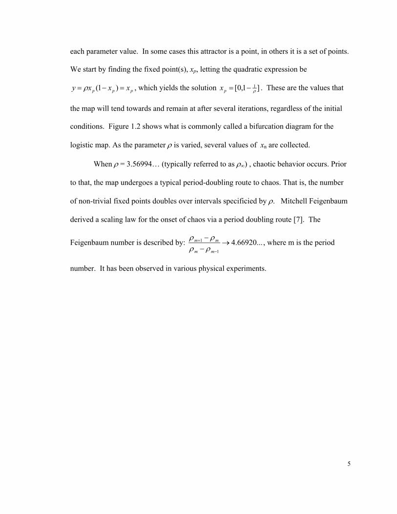
each parameter value. In some cases this attractor is a point, in others it is a set of points.
We start by finding the fixed point(s), xp, letting the quadratic expression be
ppp xxxy =−= )1(ρ , which yields the solution ]1,0[ 1ρ−=px . These are the values that
the map will tend towards and remain at after several iterations, regardless of the initial
conditions. Figure 1.2 shows what is commonly called a bifurcation diagram for the
logistic map. As the parameter ρ is varied, several values of xn are collected.
When ρ = 3.56994… (typically referred to as ρ∞) , chaotic behavior occurs. Prior
to that, the map undergoes a typical period-doubling route to chaos. That is, the number
of non-trivial fixed points doubles over intervals specificied by ρ. Mitchell Feigenbaum
derived a scaling law for the onset of chaos via a period doubling route [7]. The
Feigenbaum number is described by: ...66920.41
1 →−
−
−
+
mm
mm
ρρρρ , where m is the period
number. It has been observed in various physical experiments.

6
Figure 1.2 Bifurcation diagram for the logistic map as parameter ρ is varied.

7
One of the more noted properties of chaotic dynamics is its sensitivity to small
perturbations. Often referred to as the Butterfly Effect, referring to the notion that a
butterfly flapping its wings in China could initiate a storm in New York next month, this
property is indicative of seemingly random behavior occurring in sometimes very simple
systems. Chaotic systems do not produce random behavior, however, solutions become
increasingly uncorrelated to its initial conditions as time increases. This is best illustrated
with an example using the aforementioned logistic map. The table below shows three
separate values from the map at ρ = 4, after 10 iterations, given three initial conditions
separated by 0.01. Variations in the ending points are significantly greater than the
variation of the initial conditions. Unless the initial condition is known with infinite
precision, it becomes impossible to predict the outcome of the map for all time. The slope
of the map, xdxdy ρρ 2−= , governs the spreading of a point on the map. A true measure
of the sensitivity to small changes in this chaotic map and any other chaotic system is
called the Lyapunov exponent [7]. If we let dn be the difference between any two points
at iteration time n, the relationship dn = d02λn holds, and λ is the Lyapunov exponent. It
has been shown that the Lyapunov exponent must be positive for chaotic behavior to
exist [11].
Table 1.1 Demonstration of the spreading of initial conditions for the logistic map for ρ = 4 (chaotic).
x0 d0 x10 ∆x d10 λ
0.199 -- 0.8160 0.6170 --
0.200 0.001 0.9616 0.7616 0.1446 0.7176
0.201 0.002 0.4488 0.2478 0.3692 0.7528

8
The attractor is the point or set of points in state space that the system tends to be
drawn to. For the logistic map with a parameter value greater than ρ∞ the attactor is a set
of points that are chaotic and indeed fractal, thus the attractor is referred to as a strange
attractor. Benoit Mandelbrot coined the term fractal, where he referred to objects having
fractional dimension. There are different types of dimension, however the Hausdorff
dimension, indicated by D0, is the physical dimension that we are most familiar with, and
is often called the box-counting dimension [10]. Therefore, a chaotic system that has an
attractor whose Hausdorff dimension is non-integer is said to have a strange attractor.
The Hausdorff dimension of the logistic map has been calculated, for ρ = ρ∞, to be D0 =
0.618…, which is greater than a point (D0 = 0), but less than a line (D0 = 1).
Another interesting and important property of chaotic systems is their tendency to
synchronize with each other. Pecora and Carroll first reported this phenomena in chaotic
circuits and has since laid the foundation for a great many applications of the
synchronous behavior of chaotic circuits in practical electronics [12,13]. This property is
also intimately related to the ability of chaotic oscillators to be controlled using small
perturbations. This groundbreaking work was first introduced by Ott, Grebogi, and
Yorke [14] and has been responsible for a flood of research, development, and applied
technology in the area of chaotic dynamics. We will show how specific continuous-time
chaotic systems, such as chaotic circuits, are directly related to discrete-time chaotic
maps like the logistic map, and how the synchronization properties are crucial to the
development of technologically beneficial applications. Figure 1.3 is an illustration of
two chaotic oscillators synchronized together.

9
ChaoticOscillator
x
y
z
ChaoticOscillator
x
y
zA B
Figure 1.3 Two chaotic oscillators synchronized together. Oscillator B tracks the identical behavior ofoscillator A.
Oscillator B

10
1.3 Applications of Chaotic Dynamics
Since Ott, Grebogi and Yorke’s paper in 1990 there has been a tremendous push
for the application of chaotic dynamics to technology. Like other endeavors of the 90’s
many a student, professor and entrepreneur rushed to this area to find what gems lie
there. Technology companies have been established, employing researchers in chaotic
dynamics in order to find important links to commercial technology. Applications
ranging from the control of fluid dynamics, weather prediction and control, spacecraft
guidance, sensors and detection, and control of lasers, to various facets of
communications have been studied and in some cases put into practice.
1.4 Communication and Chaotic Dynamics
By far, the most intriguing and sought after application of chaotic dynamics is in
the area of communications. In 1993 Hayes described a formal linkage between chaotic
dynamics and information theory [15], showing that the symbolic dynamics of a chaotic
system could be controlled, thereby paving the way for encoding of digital information
into a chaotic oscillation [16]. That has been the basis for serious engineering
applications in this area. Figure 1.4 shows the oscillations of the Lorenz systems of
equations encoded to produce a pre-described digital sequence.

11
Figure 1.4 Lorenz oscillations encoded to carry a digital sequence whichproduces the ASCII text ‘c-h-a-o-s’.

12
1.5 Wireless Communications and the Opportunity
Over the past few years the intent of effort in chaotic dynamics has moved from
the arena of research to applied science, to applications engineering, to
commercialization. At the same time the communications industry has squarely trained
its focus on wireless technology. Even though there has been a significant down-turn in
the past year or so in this industry, there still remains significant optimism as consumer
demand for new features and the integration of current features continues to grow [17].
Table 1.2 below shows world mobile handset subscribers, past, present, and projected
through 2005, having a compound annual growth rate of 16.5%. Regardless of the
commercial climate, there is a large, ever-evolving market for wireless communications.
Table 1.2 Mobile Handset Market: Mobile Subscriber Forecast (World), 1999 – 2005.
Year Subscribers(Million)
New Additions(Million)
SubscriberGrowth Rate (%)
1999 477.5 159.5 -2000 722.0 244.5 51.22001 943.3 221.3 30.72002 1,151.5 208.2 22.12003 1,363.6 212.1 18.42004 1,560.1 196.5 14.42005 1,739.0 178.9 11.5CAGR 16.5%CAGR = Compound Annual Growth Rate (2001-2005)
One of the greatest challenges for the mobile wireless communications industry
has been the provision of mobile power sources capable of meeting the growing demand
by users. Improvement and integration of features in mobile handsets increase on-time,
and processor requirements, all placing higher demand on the battery. According to Frost
& Sullivan, the development of battery technology, specifically its energy storage

13
capacity, has not kept up with the demand by the mobile wireless industry [18]. The
solution to this dilemma lies in the efficient utilization of the power provided. In mobile
communications the power amplifier uses the bulk of the supply power. Table 1.3 shows
a survey of the leading power amplifier products and the performance of their products.
For a power amplifier, power added efficiency (PAE) is defined by dc
ino
PPPPAE −
= ,
where Po is the output power, Pin is the input power, and Pdc is the power delivered by the
dc source. As shown by the table, efficiencies tend not to exceed 50% in practice. This
wasted energy, often in the form of heat, is due to employment of inefficient linear design
techniques in order to meet the strict spectral requirements required by the industry.
Table 1.3. Summary of performance parameters for the leading PA products.
Raytheon RF Micro Devices IBM SirenzaPart Number RMPA0951A-102 RF2162 2018M009 SPA-2118Gain 30 dB 29 dB 28 dB 32.5 dBPAE 30%/44% 35%/50% 34%/48% 38%Harmonics -30 dBc -30 dBc -30dBc -30 dBcNoise Figure - - - 5.0 dB3rd Order Intercept 48.0 dBDynamic Range 85 dB 85 dB 85 dB 85 dB
It is well known that the operation of electronic circuits and devices in the
strongly nonlinear regions yields higher power conversion efficiency [19]. The heart of
chaotic dynamics is its operation in the nonlinear regions of the system. Figure 1.5
shows a typical I-V characteristic for a transistor. Traditional designers bias their circuit
such that the transistor is operating in the linear region. This type of operation limits the
output voltage swing of the circuit. Although the circuit may be capable of producing
output voltages outside of the linear region of the transistor, the circuit is purposely

14
designed to avoid this. Circuits that are designed to operate in the nonlinear region of the
transistor’s operation are capable of broader output voltage swings and even higher
current, thus capable of higher output power, thus capable of higher power conversion
efficiency.
Chaotic oscillations occur as a result of operating the system in its nonlinear state.
This is not to say that all nonlinear operation results in chaos, only that the system must
be nonlinear in order for chaos to exist. There is also a natural complexity to the
oscillations of a sometime very simply realized chaotic system that makes these systems
attractive for communications applications. The goal of this work is to show that
Linear Region
Nonlinear Region
Voltage swing limitation
Figure 1.5 A typical I-V characteristic curve for a transistor describing the linear andnonlinear regions of operation.
Voltage Swing (V)
CurrentSwing (A)

15
generation of chaotic signals for highly efficient amplification and transmission of digital
communications waveforms for wireless telecommunications is practical, realizable, and
technologically beneficial.

16
CHAPTER 2
A Paradigm Study: The Colpitts Oscillator
2.1 Rationale
In this chapter we will consider the Colpitts oscillator as our chaotic oscillator of
choice. There are three fundamental reasons why we choose this particular oscillator.
The first reason is that the Colpitts configuration has been a staple of communications
electronics for years. Most analog electronic circuits that require sinusoidal signal
employ Colpitts circuits. Suppose we have the general series voltage feedback system
shown in figure 2.1. The voltage gain of the amplifier section is A and the voltage
transfer of the feedback section is β. The overall gain of the system is given by,
AAAf β+
=1
. When βA = -1, or has magnitude 1 at a phase angle of 180o, then oscillation
will occur. This is known as the Barkhausen criterion [20]. The distinction of the
Colpitts circuit is in the feedback portion of the circuit. Figure 2.2 is the Colpitts circuit
used for this analysis. Note the feedback is a tank circuit consisting of an inductor and
A
β
Figure 2.1 A general voltage feedback system.
Ve
Vc
R
Re
L
Ce
C
+
Vee
Q
+
Vcc
Figure 2.2 Transistor based Colpitts oscillatorcircuit used for this analysis.

17
two capacitors. The resonant frequency is given by e
e
LCCCC +
=ω . The circuit equations
are,
where ic is the forward transistor collector current defined by ( )1−= − evc ei αγ , γ and α are
empirically derived factors for the transistor and RL is the series resistance of the
inductor.
The second reason for choosing the Colpitts oscillator is apparent from both the
circuit mathematical expression and the circuit schematic diagram. The Colpitts circuit is
a simple circuit easily modeled, easily realized, and scaleable in frequency. These are
critical factors in considering this type of architecture for practical, commercial
technology.
The third reason is that in general the chaotic dynamics produced by this
oscillator are well understood. There are parameter sets that produce chaotic oscillations
of a Rössler type. Once such set of parameters are: [Vcc = 5V, Vee = -5V, C = 1.6 nF, Ce =
1.8 nF, L = 6.8 µH, R = 62.5 Ω, RL = 2Ω, Re = 260Ω, γ = 1.06 x 10⁻¹⁵, β = 41.2]. Figure
2.3 shows the output oscillation for vc with respect to time, and figure 2.4 shows a three
dimensional plot of the solutions of the state equations for the circuit utilizing these
parameter values. The object formed is what is termed a state-space attractor, and is
( )
cLec
e
EEeL
ee
LLcCCL
iidtdvC
dtdvC
RVvi
dtdvC
iRRvVdtdiL
−+=
−−=
+−−=

18
indeed a strange attractor. Figure 2.5 shows the power spectrum for vc. Here we see the
broad spectral content typical of chaotic oscillations. The calculated resonant frequency
for the circuit, using the equation above, was 2.1 MHz.
Figure 2.3 Collector voltage versus time for the Colpitts circuit using a parameter set thatproduces Rössler type chaos.
Figure 2.4 Three-dimensional representation of the state-space trajectories for theColpitts oscillator illustrating the Rössler band.

19
Different parameter values yield different degrees of chaotic behavior. This will
become useful for tuning and optimization of performance in specific applications. In the
next section we will show how this continuous-time chaotic oscillation is related to a one-
dimensional discrete-time map, and thus derive some of the measures developed earlier
for the logistic map.
Figure 2.5 Power spectrum of the collector voltage for the Colpitts oscillator in a chaotic mode ofoperation.

20
2.2 Properties and Measures
One of the most significant tools in the analysis of chaotic dynamics is the
Poincaré surface of section [5]. Named for the early 20th century French mathematician
Henri Poincaré, the Poincaré surface of section is a way of reducing a three-dimensional
continuous-time flow to a discrete-time map by placing a two-dimensional surface in the
path of the flow and extracting the points that pierce that surface. Figure 2.6 illustrates
the placement of such a surface in the state-space for the attractor of figure 2.4. Figure
2.7 shows the resulting Poincaré map while figure 2.8 gives the return map for the
collector voltage. Although these maps appear to be one-dimensional, and can be
approximated as such, there is a highly compressed Cantor set fractal that governs the
placement of each point of the mapping [13]. Note the similarities of the return map to
the logistic map.
Figure 2.6 Chaotic attractor for the Colpitts oscillator with an Poincaré surface ofsection erected in the flow.

21
Figure 2.7 Poincaré map produced by the surface of section in figure 2.6.
Figure 2.8 Return map for the collector voltage as produced by sequential observation ofpoints generated by the Poincaré mapping. Note its resemblance to the logistic map.

22
Given the similarity to the logistic map we can calculate a Lyapunov exponent in
a similar fashion. It is important to note that Lyapunov exponents are dependent upon the
region of state-space from which the trajectories originate. Large, positive exponents
indicate regions of tremendous expansion of the attractor while smaller exponents
indicate a slower rate of expansion. Both actions are necessary for chaotic motion.
Chaotic oscillations achieve a balance between instability and degeneration, thus we have
termed these oscillations as bounded instabilities. Table 2.1 shows calculated Lyapunov
exponents for two sets of points using the Colpitts oscillator discrete-time mapping. The
results illustrate the compression and expansion of the flow.
Table 2.1 Calculation of local Lynapunov exponents for the discrete time mapping of the Colpittsoscillator.
v0 d0 vN dN λ
-14.1593 -- -17.0695 --
-14.0679 0.0915 -14.0679 3.0016 0.5036
-12.427 --- -13.2497 ---
-12.4248 0.0022 -13.1887 0.0610 0.4793

23
2.3 The Colpitts Oscillator as a Digital Signal Source
If we take a further step and assign a partition boundary to the discrete-time return
map for the chaotic flow, we can produce a unique symbolic representation of the
dynamics of the system [21]. A natural partition boundary exists at the peak of the map.
The partition also lends itself to the simplest symbolic representation, binary. Figure 2.9
shows the assignment of the symbolic dynamics to the return map and indicates how
binary information is generated by the oscillations. Figure 2.10 shows how this partition
is related to the Poincaré map, which is directly related to the chaotic flow.
Figure 2.9 The return map for the Colpitts chaotic oscillator illustrating the binary partition and thegeneration of digital information.

24
We can take this analysis a step further by considering the N-bit binary sequences
generated when a trajectory crosses a particular point on the Poincaré surface. This is
done by integrating the system forward in time and capturing the bits in an N-bit register
as state-space trajectories cross the surface. The result is the N-bit coding function that
gives the proper state-point necessary for generating a given binary sequence. We show
an example of this coding function for 8-bit binary sequences in figure 2.11. The 8-bit
sequences are represented by their decimal numbers from 0 – 255 (00000000 –
11111111). The parameter set used to generate the chaotic oscillation produce highly
constrained symbolic dynamics. This is evident from the attractor in figure 2.6. Note that
Figure 2.10 The Poincaré map of the Colpitts chaotic oscillation showing the placement of the binarypartition boundary. Trajectories passing through the Poincaré surface of section on either side of theboundary produce bit 0 or 1.

25
the band of chaotic trajectories is then and does not fill the state space from the center
outward. As a result, only 20 of the possible 255 8-bit binary sequences are generated for
the number of integration steps taken.
The Poincaré surface of section is placed at a point in the state space where iL =
0.05 A. Each binary sequence is uniquely associated with a collector voltage via the
coding function and a emitter voltage via the Poincaré map. The conclusion is that there
is a unique point in state space that will be a source for a distinct binary sequence. This
point can be used as an initial condition to encode binary information into the chaotic
oscillations. Hayes work involved using small perturbations to control a chaotic
Figure 2.11 8-bit binary coding function for the Colpitts oscillator.

26
oscillator to produce any desired digital stream [15]. We show an example by encoding
the 8-bit binary sequence 01011101 (decimal 93).
According to our coding function and Poincaré map, the initial condition that will
source this sequence in the chaotic oscillation is iL = 0.05, ve = -0.7438, and vc = -
15.7858. Figure 2.12 shows this oscillation in state space while figure 2.13 shows the
collector voltage with respect to time with the Poincaré surface crossings marked to show
the binary encoding.
Figure 2.12 State-space trajectories encoded to produce the 8-bit binary sequence 01011101.

27
So far we have shown that a chaotic oscillator can be used as a binary signal
source. Work has been done to provide further advances in the implementation of
chaotic oscillators as digital signal generators. Innovations such as segment hopping [18]
and band-limited, digitally encoded chaotic waveforms for base-band signaling [19] are
being prepared for commercialization. The simplicity and efficiency of electronic chaotic
oscillators are the primary attraction for technologists. In the next section we outline an
implementation of chaotic dynamics to communication technology that provides
tremendous advantage over traditional design.
Figure 2.13 Time-varying collector voltage demonstrating the 8-bit binary encoding 01011101embedded into the oscillations.

28
2.4 Syncrodyne Amplification
The general concept of “controlling chaos” encompasses many different
approaches. The first method to become widely accepted was the method of Ott, Grebogi,
and Yorke, and became referred to as the OGY method of controlling chaos [10]. This
method is essentially proportional feedback, and is used to control a chaotic oscillator so
that it produces a periodic orbit. A control pulse is applied to a system with the pulse
energy being proportional to the error from the desired periodic orbit. This method can
also be used for symbolic dynamics control we referred to in the previous section. For
symbolic control, the error is measured from the point in state space that sources the
desired symbol sequence instead of a periodic point, and a proportional control pulse is
applied to correct this error. One can also use continuous-time feedback control, and
continuously correct the error from the desired trajectory in state space.
The problem with feedback methods for high frequency oscillators is their latency
time. The controller must detect the error in state space, typically at the Poincaré surface
of section, and then compute and apply a control pulse proportional to this error. This
computation, be it digital or analog, takes time, and this loop delay can become a
significant fraction of the Poincaré return time for rf oscillators. The synchronization
property of chaotic systems provides an intriguing opportunity for engineering
application.
The Syncrodyne amplifier based on the concept of signal amplification using
synchronous dynamics. Syncrodyne amplification is the process of locking a chaotic
oscillator, larger in power, to a smaller, continuous-time, information-bearing oscillator.
The smaller oscillator is called the guide signal. The key is that the guide signal is

29
capable of carrying arbitrary digital information. Information transfer and power
amplification is achieved.
The continuous-time guide signal has the advantage of only needing to guide one
state variable. The guide signal need only supply a small amount of power to the
"amplifying oscillator" in order to stabilize its dynamics. The result is that this type of
continuous-time control of chaos acts as a signal amplifying means with great potential
for digital communication applications. Figure 2.14 shows a simple block diagram of a
syncrodyne amplifier. As synchronization occurs, the error signal, e(t) goes to zero. In a
practical application, which we will describe shortly, this error is directly related to the
current flow from the guide system to the output oscillator. As the current goes to zero
the power flow from guide to output goes to zero and power amplification occurs.
InputSignal
ChaoticOscillator
guide signal g(t)
output signal o(t)error signal e(t) = o(t) – g(t)
Figure 2.14 Block diagram of a Syncrodyne amplifier system.

30
It was once thought that this process would only apply to a guide oscillation and
an output oscillation that has similar, if not exact, dynamical behavior. We show that this
is indeed not the case. We show that the guide signal can be phase modulated sinusoidal
oscillations such as phase shift keying (PSK), quadrature phase shift keying (QPSK),
minimal shift keying (MSK) and even more sophisticated communications signal formats
applicable to the global system for mobile communication (GSM) and code-division
multiple access (CDMA). This leads to the application of this technique to standard
digital communications technology, offering the possibility of high-gain, high efficiency
power amplification.
We will use our Colpitts oscillator as our primary example. Consider the circuit
shown in figure 2.15. It is the same as the earlier circuit although it is modified to accept
an input signal at the emitter voltage node. The resistor Rin controls the input signal
current. The circuit equations are modified as such,
( )
cLec
in
ein
e
EEeL
ee
LLcCCL
iidt
dvCdt
dvC
Rvv
RVvi
dtdvC
iRRvVdtdiL
−+=
−+
−−=
+−−=
Vin
Rin
Ve
Vc
R
Re
L
Ce
C
+
Vee
Q
+
Vcc
Figure 2.15 Circuit schematic diagram for aColpitts oscillator based syncrodyne amplifier.

31
We will use this circuit to carry out our analysis via a MATLAB mathematical model.
We will show results for sinusoidal input signals in the next section.
2.5 Modeling Results and Analysis
Before we show a series of results from our computer model we will first define
some measures used in the analysis. First, we’ve chosen circuit parameters that put the
resonant frequency near 2 MHz. Table 2.2 shows the values for the circuit used.
Table 2.2 Circuit parameter values used for syncrodyne amplifier model analysis.
Circuit Parameter Value
C (varied) 1 – 3 nF
Ce 1.8 nF
Re 260 Ω
RL 2 Ω
R 62.5 Ω
L 6.8 µH
Vcc 5 V
Vee -5V
γ 1.06 x 10⁻¹⁵
α 41.2
Since we are analyzing the performance of a power amplifier the important
measures are the power gain, Gp, and the power added efficiency, PAE. The gain is
simply defined by Gp = 10log(Po/Pin), where Po is the output power delivered to the load
and Pin is the input power from the signal source. In this case we use Re as the load. The
32
power added efficiency is an important measure in power amplifier analysis because it
takes into account the power added by the source in its calculation. It is a much truer
measure of the efficiency in such a case. In the model we calculate these power quantities
by averaging over several cycles, thus obtaining these measures using average power.
The following are the relationships between the power quantities and obtainable circuit
values:
Pdc = Pcc + Pee
Pcc = VcciL
Pee = VeeiRe = eee
eee VR
vV −
Pin = viniin = inin
ein vR
vv −
Po = ee
eee RR
vV2
−
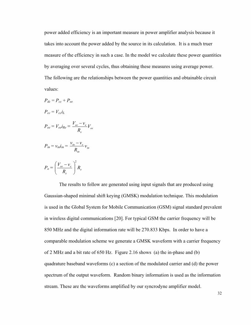
The results to follow are generated using input signals that are produced using
Gaussian-shaped minimal shift keying (GMSK) modulation technique. This modulation
is used in the Global System for Mobile Communication (GSM) signal standard prevalent
in wireless digital communications [20]. For typical GSM the carrier frequency will be
850 MHz and the digital information rate will be 270.833 Kbps. In order to have a
comparable modulation scheme we generate a GMSK waveform with a carrier frequency
of 2 MHz and a bit rate of 650 Hz. Figure 2.16 shows (a) the in-phase and (b)
quadrature baseband waveforms (c) a section of the modulated carrier and (d) the power
spectrum of the output waveform. Random binary information is used as the information
stream. These are the waveforms amplified by our syncrodyne amplifier model.

33
(a)
(b)

34
(c)
(d)
Figure 2.16 (a) In-phase and (b) quadrature baseband components of a 2 MHz GSM waveformalong with (c) the modulated carrier and (d) the power spectrum.

35
A significant finding was that the capacitor C acted as an optimization element for the
gain and the efficiency. We were able to maintain stable, repeatable chaotic dynamic in
the circuit over a range of 1 nF to 3 nF. First we saw that the size of the attractor change
as this element was varied. If we create a fictitious measure called the attractor volume,
derived by calculating the volume of a cube created from the maximum and minimum
values from the inductor current, emitter voltage and collector voltage, we can see the
relationship of the chaotic attractor to this capacitance. Figure 2.17 shows the
relationship over a range of capacitance.
In the wireless handset power amplifier industry, the key challenge is the power-added
efficiency. Typical power gain performance is about 30-dB. There are other industries,
Figure 2.17 Variation of the attractor volume as the capacitor C is changed.

36
such as satellite and base-stations, that may benefit from enormous power gains. The
output signal power was maximum at about 25 dBm. We found that this tuning capacitor
also allowed us to find points of enormous power gain. We surmise that these are points
where the energy required to bring the chaotic oscillator in compliance with the source
signal is nearly nonexistent. Figure 2.18 shows an example of power gains in excess of
60 dB for a given capacitor value. At this point we are not prepared to state that this
relationship between the capacitance and the gain has a fractal structure to it, although it
is possible. From a practical standpoint, we used an optimization algorithm to find the
best capacitor value and similar procedures could be implemented with tuning capacitors
such as varactors.
Figure 2.18 Power gain as a function of the tuning capacitance C.

37
As expected the efficiency of the amplifier was directly related to the peak-to-
peak voltage of the input signal. The tuning capacitance also affected the efficiency. We
were able to calculate a relationship between the peak-to-peak input voltage, the tuning
capacitance and the power-added efficiency. This will allow a designer to determine the
optimal range of operation for the amplifier. Figure 2.19 is a surface map that illustrates
this graphically. Note that there is a wide range of operation for a designer to achieve
70% PAE or better from this system.
PAE > 70%
Figure 2.19 Surface map illustrating the PAE for peak-to-peak input voltages andtuning capacitance values.

38
In a similar manner we were able to calculate curves for the maximum power gain
as the peak sinusoidal input voltage was varied. This acts as a complementary design
tool. Figure 2.20 is a plot of this relationship. Higher power gains are probably possible
as we tune the asymptotic relationship between the tuning capacitance and gain. We
wanted, however, to stay within the bounds of realizable capacitor values. Finally we
were able to determine the relationship between the optimal power gain and the optimal
PAE for this system. This relationship is shown in figure 2.21.
Figure 2.20 Relationship between the peak power gain and the peak sinusoidal input voltage forthe syncrodyne amplifier circuit.

39
In traditional power amplifier systems you would expect to find a linear, inverse
relationship between gain and efficiency. In this system the relationship is not simple. It
suggests that high gain and high efficiency are possible in various regions of operation.
The tradeoff appears to be in the system stability. It is difficult to maintain the areas of
extremely high gain in practice. System noise and component tolerances will make the
tuning of extremely high-gain points impractical. Practical gain numbers should be about
40-dB.
The goal of this work was to define and analyze a chaotic circuit capable of acting
as a digital signal source. Not only have we modeled such a system that acts as a direct
digital encoder by producing a binary symbolic dynamics, we have further modeled a
Figure 2.21 Overall PAE peak power gain relationship for the syncrodyne amplifier circuit. Notethat there are regions of operation where the system is capable of nearly 80% PAE and greater than55 dB gain.

40
system capable of providing ultra-high power amplification and high power-added
efficiency to standard communications waveforms such as GSM. We take this work a
step further by carrying out the design, fabrication, and testing of the 2 MHz syncrodyne
amplifier described in this chapter, and provide a formal approach for the design of a 850
MHz chaotic oscillator for implementation of the syncrodyne approach at PCS (personal
communications systems) frequencies. This is outlined in the next chapter.

41
CHAPTER 3
Custom RF Chaotic Oscillator Design
3.1 Design Criteria
In this chapter will the outline the fabrication and testing of a 2 MHz syncrodyne
amplifier circuit and also show preliminary modeling results for an 850 MHz circuit. We
began by looking at the modified circuit schematic diagram used in a PSPICE analysis,
and use this for the basis for the PCB layout. Figure 3.1 shows a schematic diagram of
this circuit.
One of the critical features of this circuit will be its ability to be tuned to different
types of behavior. As we outlined in the first chapter, there are different types of
dynamics that can be present in one chaotic system. We will need to be able to tune the
circuit so that it produces the type of chaotic behavior we want to work with and also be
able to tune the chaos to some of the different states possible within it. The variable
resistors Re and R1 are good for tuning the circuit from periodic behavior to the desired
chaotic states. Once there, CT is a variable capacitor used to maximize the gain and
efficiency. Resistor Rin is used to adjust the synchronization of the input signal in order
to maximize the performance. The figure also shows the element values used to realize
this circuit.
The type of chaotic behavior desired is the simply folded band, which is a general
description of a Rössler band, typical of a Colpitts oscillator in a chaotic state. Many
other circuits produce Rössler-type behavior [21]. We have already shown how this type
of chaotic motion is related to the single-humped, one-dimensional logistic map through
the Poincaré surface of section. The analysis of these types of systems are more

42
manageable than more complex types of chaotic motion.
Circuit Element Values
L1 4.7 µHL2 2.2 µHR1 1 – 100 ΩRin 1 – 10 ΩRe 1 – 500 ΩCbase 1.5 nFCT 100 – 1000 pFCe 1.8 nF
Figure 3.1 2 MHz syncrodyne amplifier circuit schematic diagram.
vin
Rin
A+
iL
vc
Re
P1
L1
CT
ve
Ce
Cbase
+
Vee
T1
L2+
Vcc

43
3.2 PSPICE Modeling
We were successful in generating a SPICE model for a 2 MHz chaotic oscillator
capable of acting as a digital signal source via the control of symbolic dynamics and the
application of syncrodyne amplification. The circuit schematic diagram of figure 3.1 was
captured directly from the SPICE modeling package TINA. The following figures show
the results from the model. The circuit is only slightly chaotic. The extreme limitations
of the software to tune the circuit presented problems in generating various states of
chaotic motion. As we will see in the following section, the actual fabricated circuit was
more amenable to tuning.
Figure 3.2 shows a two dimensional projection of the state-space attractor,
showing the inductor current versus the emitter voltage, which acts as our output. There
is a small band of chaotic trajectories as the circuit settles into its steady-state from the
initial off state. Note the slight fold that occurs in the trajectories. This action is
necessary for simple chaotic motion. It was very easy to get this system to oscillate,
however it was difficult to find broad chaotic motion. Figure 3.3 shows how the emitter
voltage signal varies with respect to time. Note the irregular occurrence of the peaks.
Figure 3.4 is the frequency spectrum of the emitter voltage signal. This demonstrates the
broad frequency content typical of chaotic oscillations. The other important point is that
this circuit architecture provides a method of producing chaotic motion that restricted to a
limited frequency band. The property is attractive for communications applications,
particularly wireless communications.

44
Figure 3.2 Two-dimensional projection of the chaotic attractor produced by the 2 MHz Colpittsoscillator SPICE simulation.
Figure 3.3 Time-dependent oscillation of the emitter voltage in a slightly chaotic state.

45
Figure 3.4 Frequency spectrum of the emitter voltage oscillations illustrating the broadfrequency content indicative of chaotic behavior.

46
3.3 Circuit Fabrication and Testing
Figure 3.5 is a photograph of the fabricated 2 MHz Colpitts based chaotic circuit.
The PCB layout illustrated in figure 3.6 was populated with circuit elements to realize
the syncrodyne amplifier modeled in the last section. Some general measurements were
taken. There was good agreement between the behavior of the mathematical model, the
PSPICE model, and the fabricated circuit.
Figure 3.5 Photograph of the fabricated 2MHz syncrodyne amplifier circuit.
Figure 3.6 Picture of the PCB used to fabricate the 2 MHz syncrodyne amplifier circuit.

47
Figure 3.7 shows a measured time-dependent output signal from the circuit. Like
the simulation, the chaotic motion is indicated by the irregular occurrence of the peaks
and valleys. This, and the following measurements, were taken using a 40 Msps
National Instruments sampling card. We had only one sampling channel available at the
time of this measurement, allowing only one state-variable to be sampled at a time.
Figure 3.8 shows the output data of the chaotic oscillator under symbolic dynamics
control producing a constrained binary signal. First, the two-dimensional projection of
the attractor is formed not by plotting two state-variables against themselves, but by
Figure 3.7 Measured time signal from the Colpitt’s oscillator circuit.

48
plotting one state variable versus a time-delayed copy of itself. This method is called
time delay embedding and is useful when only one state variable of a chaotic system is
available [22]. It is still possible to obtain a fairly accurate representation of the
dynamics by using this method. The constraint on symbolic dynamics was introduced by
disallowing any binary sequence that contained more than two consecutive zeroes. For
example the sequence B1 = 11100101 would be allowed as an input, but the sequence B2
= 11100010 would not. There specific, identifiable regions of state-space that would
produce sequenced with more than two zeroes present. These regions would never be
visited by the trajectories, thus the gaps in the attractor.
Fig. 3.8 The Colpitts attractor controlled on a constrained set. The Cantor set structure isa result of the constraint.

49
As we progressed in the testing phase of this project we were able to obtain a
sampling card with two input channels. We were then able to measure two state variable
simultaneously. Figure 3.9 shows a two-dimensional projection of the attractor using the
voltage across the inductor, vL, and the voltage across the collector capacitor. The
inductor voltage is directly related to the inductor current iL, which was used for earlier
analysis. This attractor is produced using the chaotic circuit uninfluenced by any control
signal. Figure 3.10 shows the same circuit controlled on a Cantor set using a constrained
input binary sequence.
Fig. 3.9 Uncontrolled 2 MHz Colpitts attractor showing a two-dimensional projectionof the state-space attractor.

50
Finally, we took measurements to demonstrate the syncrodyne amplification
properties of the system. Figure 3.11 shows (a) the input signal, (b) the output signal and
(c) the error signal. Although voltages are the same, the input power delivered as
compared to the output power is extremely small, hence the enormous gain. Figure 3.12
shows comparisons of the measured experimental data with the modeled the data
calculated earlier.
Fig. 3.10 Symbolic dynamics controlled Colpitts attractor.

51
Fig. 3.11 Results from the 2 MHz syncrodyne amplifier circuit showing (a) the input signal, (b) theoutput signal and (c) the error signal.
(a)
(c)
(b)

52
Figure 3.12 Comparison of experimental data from the 2 MHz syncrodyne amplifierwith modeling results.
53
3.4 Preliminary Design of a 850 MHz Circuit
In order to suggest the feasibility of applying this technique to commercially
viable communications systems we must show that it is possible to design such circuits at
the frequencies of operation and have it capable of handling the types of signal formats
used in them. A typical frequency band used in personal communications systems (PCS)
is 824-850 MHz. Both CDMA and GSM, the dominate signal formats in the industry, are
transmitted over this band [20].
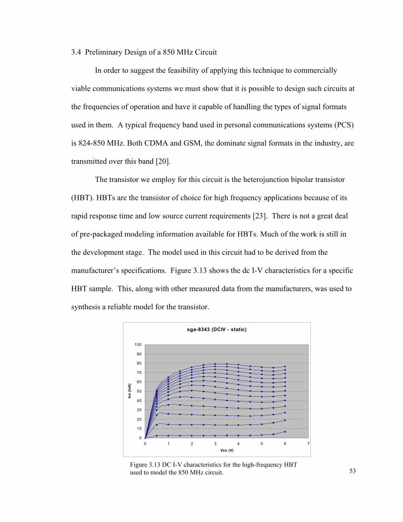
The transistor we employ for this circuit is the heterojunction bipolar transistor
(HBT). HBTs are the transistor of choice for high frequency applications because of its
rapid response time and low source current requirements [23]. There is not a great deal
of pre-packaged modeling information available for HBTs. Much of the work is still in
the development stage. The model used in this circuit had to be derived from the
manufacturer’s specifications. Figure 3.13 shows the dc I-V characteristics for a specific
HBT sample. This, along with other measured data from the manufacturers, was used to
synthesis a reliable model for the transistor.
sga-8343 (DCIV - static)
0
10
20
30
40
50
60
70
80
90
100
0 1 2 3 4 5 6 7Vce (V)
Ice
(mA
)
Figure 3.13 DC I-V characteristics for the high-frequency HBTused to model the 850 MHz circuit.

54
The circuit schematic diagram shown in figure 3.14 shows the Colpitts type
circuit fashioned to implement a chaotic oscillator using this architecture. We have found
that in the “search for chaos” the first, best place to start is the biasing structure
supporting the transistor. Here R1 and Rb provide the first level of tuning to find regions
of bounded instability. We attempted to keep Vcc around 3 V dc in order to be near the
source voltages used in commercial practice.
Figure 3.15 shows a time dependent oscillation of this slightly chaotic waveform.
Note the variations in the valleys of the waveform. Again, restrictions on the ability to
tune using the SPICE software limited our ability to find regions of highly chaotic
motion. Our past experience tells us that a fabricated circuit will have more regions
available for tuning. Figure 3.16 shows a two-dimensional projection of the state-space
T1
Rb
Cc
A +
iL
VC2
R1
VC1L
C1
C2
+
Vcc
Figure 3.14 Schematic diagram of the high-frequency, Colpitts type, chaotic oscillator modeledusing an HBT.

55
using the inductor current and the voltage across C2 as variables. Note the slight fold that
occurs in the trajectories. It can be argued that this is a 4-dimensional system (there are 4
independent variables) and that the chaotic attractor is higher than three dimensions.
Finally, Figure 3.17 shows the frequency spectrum of the voltage across Capacitor 1. Its
center frequency is about 836 MHz, which is center of the 824-850 MHz band.
Figure 3.15 Time dependent oscillation of the voltage vC1 for the 850 MHz chaotic oscillatorsimulation.

56
Figure 3.16 Two-dimensional projection of the state-space for the 850 MHz chaoticoscillator simulation.
Figure 3.17 Frequency spectrum for the voltage across C1 for the 850 MHz chaoticoscillator simulation.

57
CHAPTER 4
Conclusion
4.1 Discussion of Results
The purpose of this work was to demonstrate that a chaotic source could be
synthesized that could be used to produce radio-frequency signals capable of carrying
digital information. We began by showing that a discrete-time mapping called the
logistic map, which is a basic, fundamental paradigm of chaotic behavior, is directly
related to the Colpitts oscillator, which has been a cornerstone of communications
technology for years. We were able to show that important measures of chaotic
dynamics behavior, evident in the logistics map, were also present in mathematical
models of the Colpitts oscillator. Further, we were able to show that it was possible to
encode arbitrary binary information into the oscillations of the Colpitts circuit when in it
was in a chaotic state, and it was also possible to achieve high-gain, high-efficiency
power amplification of general communications signals such as CDMA and GSM, a
process we’ve called syncrodyne amplification.
The mathematical model we derived was based upon the three-dimensional
system of nonlinear differential equations that resulted from the Colpitts circuit. With it
we showed how the synchronization property of chaotic systems was useful for
syncrodyne amplification. We also were able to develop new relationships and measures
such as the attractor volume and its relationship to the tuning parameter of the system.
For the syncrodyne amplifier, we were able to show a functional relationship between the
output power gain and the power added efficiency (PAE), demonstrating that nearly 60

58
dB gain and 80% PAE were possible. We were able to use the model to produce design
tools which provide guidance in the fabrication of a circuit at 2 MHz.
We were successful in designing, laying out, fabricating and testing a chaotic
oscillator that operated at 2 MHz. We used this circuit to empirically demonstrate the
capability of encoding digital information directly into chaotic oscillations at about 1.67
Mbps. We also demonstrated a new method for power amplification called syncrodyne
amplification. This circuit was able to provide over 40-dB power gain and over 72%
power added efficiency.
Finally, we were able to detail some preliminary design criteria for a chaotic
oscillator which operates in the 824-850 MHz band used in PCS applications. We used
manufacturer specifications to derive a complete SPICE model for a heterojunction
bipolar transistor (HBT) which acted as the nonlinear element in the circuit. We showed
the resulting chaotic attractor, time waveforms, and the frequency spectrum of the output.
59
4.2 Implications
In response to customer demand manufacturers are introducing products capable
of operating with higher speed 3G mobile services and adding new power hungry
applications, such as wireless Internet, palm top computing, and integrating PDA and
PCS functions. Battery life, which has been a principal concern of designers and end-
users, will be further taxed by these feature rich handsets. A recent Frost & Sullivan
report stated that current battery chemistries have reached their peak in their capabilities.
Either new battery technologies must be produced now (which is unlikely) or there has to
be more efficient use of the power provided. Without any improvement in battery life
handset innovation will stagnate while demand continues to soar.
To solve this problem designers have concentrated on improving the efficiency of
rf power amplifiers. Greater amplifier efficiency leads to simpler and less costly hand-
held devices, increased battery life, and increased transmission speeds and distances.
However, traditionally designed power amplifiers trade-off power gain or amplification
for DC conversion efficiency and cannot yield the efficiency that the market requires.
What is needed is a radical new approach to amplification. One that demonstrates
dramatic improvement in not only power gain but conversion efficiency, signal distortion
and power out capability. Nonlinear systems are inherently more efficient than linear
systems. Chaotic systems are nonlinear systems that produce bounded instabilities that
are being identified as beneficial for technological applications. Very high efficiency is
also possible without signal distortion, because the Syncrodyne™ amplifier uses
nonlinear dynamics in a natural way. The nonlinear operation is not an obstacle as it is in
traditional designs, but is built into the way that the amplifier works from the start. The
60
demonstrated application of controlling symbolic dynamics for the encoding of digital
information into chaotic oscillations, and the application of syncrodyne amplification for
high-gain, high-efficiency power amplification is scalable in frequency, suggesting that
devices operating well into the microwave frequency range and beyond are not far away.
In a general sense the introduction of bounded instability devices into the
mainstream of technology applications and commercial engineering has the promise of
improvements in a myriad of ways. More efficient devices are possible. Complex
operations from very simple structures are possible. More importantly we are making the
important step of taking these ideas beyond the confinements of research and thrusting
them into the arena of engineering arts. In this work we’ve considered only a small piece
of the possible areas of implementation, yet the potential impact on commercial
technology can be huge.
Finally, we are optimistic about contributing to the general body of scientific and
engineering knowledge. The promise of important applications and profitable industry
impact can be a driver of increased study into this area of nonlinear dynamics, bounded
instabilities, and their impact on technology. It is our intention to provide a basis for
deeper investigation into this important phenomenon.

61
APPENDIX A – MATLAB Procedures for Modeling and Analysis
(All code is proprietary information and property of Syncrodyne Systems Corporation © 2002 All Rights
Reserved)
Colpitts Circuit Model Equations File (Colpitts.m)
function ds = Colpitts(Vcc,Vee,L,RL,C,Ce,Re,R,alpha,Bta,s)% Function models a Colpitt's Oscillator% A three dimensional set of nonlinear differential equations% FUNCTION NAME: Colpitts.m% INPUT: Vcc - collector voltage (Volts)% INPUT: Vee - emitter voltage (Volts)% INPUT: L - inductance (Henries)% INPUT: RL - inductor resistance (Ohms)% INPUT: C - capacitance (Farads)% INPUT: Ce - emitter capacitance (Farads)% INPUT: Re - emitter resistance (Ohms)% INPUT: R - variable resistance (Ohms)% INPUT: alpha - transistor exponential parameter (V^-1)% INPUT: Beta - transistor multiplier parameter (A)% INPUT: s - initial conditions [s(1),s(2),s(3)] = [iL,ve,vc]% OUTPUT: ds - differential values (diL/dt,dve/dt,dvc/dt)% DATE WRITTEN: December 21, 1999% DATE MODIFIED: December 21, 1999% PROGRAMMER: Chance M. Glenn, Director of Technology Development% (c) 1999 NextWave Technologies, Inc.% SYMDYNE TRANSMITTER Projectds(1) = (Vcc-s(3)-(R+RL)*s(1))/L; %iLds(2) = (s(1)-((s(2)-Vee)/Re))/Ce; %Veds(3) = (C*ds(2)+s(1)-ic(alpha,Bta,s(2)))/C; %Vc
Colpitts Circuit Model Equations File for Synchronization (ColpittsSync.m)
function ds = ColpittsSync(Vcc,Vee,L,RL,C,Ce,Re,R,alpha,Bta,s,vC,RC)% Function models a Colpitt's Oscillator% A three dimensional set of nonlinear differential equations% FUNCTION NAME: Colpitts.m% INPUT: Vcc - collector voltage (Volts)% INPUT: Vee - emitter voltage (Volts)% INPUT: L - inductance (Henries)% INPUT: RL - inductor resistance (Ohms)% INPUT: C - capacitance (Farads)% INPUT: Ce - emitter capacitance (Farads)% INPUT: Re - emitter resistance (Ohms)% INPUT: R - variable resistance (Ohms)% INPUT: alpha - transistor exponential parameter (V^-1)% INPUT: Beta - transistor multiplier parameter (A)% INPUT: s - initial conditions [s(1),s(2),s(3)] = [iL,ve,vc]% OUTPUT: ds - differential values (diL/dt,dve/dt,dvc/dt)% DATE WRITTEN: December 21, 1999% DATE MODIFIED: December 21, 1999

62
% PROGRAMMER: Chance M. Glenn, Director of Technology Development% (c) 1999 NextWave Technologies, Inc.% SYMDYNE TRANSMITTER Projecticouple = (vC-s(3))/RC; % Couplingexpressionds(1) = (Vcc-s(3)-(R+RL)*s(1))/L; %iLds(2) = (s(1)-((s(2)-Vee)/Re))/Ce; %Veds(3) = (C*ds(2)+s(1)-ic(alpha,Bta,s(2))+icouple)/C; %Vc
Collector Current Equation for Transistor (iC.m)
function iout = iC(alpha,Bta,v)% Function models the collector current for a% 2N3904 transistor% FUNCTION NAME: iC.m% INPUT: alpha - transistor exponential parameter (V^-1)% INPUT: Beta - transistor multiplier parameter (A)% INPUT: v - input voltage (V)% OUTPUT: iout - collector current (A)% DATE WRITTEN: December 21, 1999% DATE MODIFIED: December 21, 1999% PROGRAMMER: Chance M. Glenn, Director of Technology Development% (c) 1999 NextWave Technologies, Inc.% SYMDYNE TRANSMITTER Projectiout = Bta *(exp(-alpha*v)-1.0);
Euler Integration for Colpitts (Integrate_C.m)
function sout =INTEGRATE_C(Vcc,Vee,L,RL,C,Ce,Re,R,alpha,Bta,dt,Npts,s0)for i = 1:Npts sout(1,i) = s0(1); sout(2,i) = s0(2); sout(3,i) = s0(3); s0 = s0 + dt*Colpitts(Vcc,Vee,L,RL,C,Ce,Re,R,alpha,Bta,s0);end
Euler Integration for Synchronized Colpitts (Integrate_CSync.m)
function sout =INTEGRATE_CSync(Vcc,Vee,L,RL,C,Ce,Re,R,alpha,Bta,dt,Npts,s0)for i = 1:Npts sout(1,i) = s0(1); sout(2,i) = s0(2); sout(3,i) = s0(3); s0 = s0 + dt*Colpitts(Vcc,Vee,L,RL,C,Ce,Re,R,alpha,Bta,s0);end

63
Poincaré Surface of Section Calculation (PSSCHK.m)
% Function that checks for and returns the Poincare surface of% section coordinates% s0 - data point 0% s - next data point% PSSD - Poincare surface coordinates [3,2]% 1-x,2-y,3-z ,1-x0,2-xffunction PSSout = PSSCHK(s0,s,PSSD)PSSout = [0.0;0.0;0.0];if PSSD(1,1) == PSSD(1,2) % Constant X surface if ((s(1)<=PSSD(1,1))&(s0(1)>=PSSD(1,2))) pssX = INTERP(s0(1),s(1),s0(2),s(2),PSSD(1,1)); pssY = INTERP(s0(1),s(1),s0(3),s(3),PSSD(1,1)); if(pssX>=PSSD(2,1))&(pssX<=PSSD(2,2))&(pssY>=PSSD(3,1))&(pssY<=PSSD(3,2)) PSSout(1) = 1.0; PSSout(2) = pssX; PSSout(3) = pssY; end end if ((s(1)>=PSSD(1,1))&(s0(1)<=PSSD(1,2))) pssX = INTERP(s0(1),s(1),s0(2),s(2),PSSD(1,1)); pssY = INTERP(s0(1),s(1),s0(3),s(3),PSSD(1,1)); if(pssX>=PSSD(2,1))&(pssX<=PSSD(2,2))&(pssY>=PSSD(3,1))&(pssY<=PSSD(3,2)) PSSout(1) = 1.0; PSSout(2) = pssX; PSSout(3) = pssY; end endendif PSSD(2,1) == PSSD(2,2) % Constant Y surface if ((s(2)<=PSSD(2,1))&(s0(2)>=PSSD(2,2))) pssX = INTERP(s0(2),s(2),s0(1),s(1),PSSD(2,1)); pssY = INTERP(s0(2),s(2),s0(3),s(3),PSSD(2,1)); if(pssX>=PSSD(1,1))&(pssX<=PSSD(1,2))&(pssY>=PSSD(3,1))&(pssY<=PSSD(3,2)) PSSout(1) = 1.0; PSSout(2) = pssX; PSSout(3) = pssY; end
end if ((s(2)>=PSSD(2,1))&(s0(2)<=PSSD(2,2))) pssX = INTERP(s0(2),s(2),s0(1),s(1),PSSD(2,1)); pssY = INTERP(s0(2),s(2),s0(3),s(3),PSSD(2,1)); if(pssX>=PSSD(1,1))&(pssX<=PSSD(1,2))&(pssY>=PSSD(3,1))&(pssY<=PSSD(3,2)) PSSout(1) = 1.0; PSSout(2) = pssX; PSSout(3) = pssY; end endendif PSSD(3,1) == PSSD(3,2) % Constant Z surface

64
if ((s(3)<=PSSD(3,1))&(s0(3)>=PSSD(3,2))) pssX = INTERP(s0(3),s(3),s0(1),s(1),PSSD(3,1)); pssY = INTERP(s0(3),s(3),s0(2),s(2),PSSD(3,1)); if(pssX>=PSSD(1,1))&(pssX<=PSSD(1,2))&(pssY>=PSSD(2,1))&(pssY<=PSSD(2,2)) PSSout(1) = 1.0; PSSout(2) = pssX; PSSout(3) = pssY; end end if ((s(3)>=PSSD(3,1))&(s0(3)<=PSSD(3,2))) pssX = INTERP(s0(3),s(3),s0(1),s(1),PSSD(3,1)); pssY = INTERP(s0(3),s(3),s0(2),s(2),PSSD(3,1)); if(pssX>=PSSD(1,1))&(pssX<=PSSD(1,2))&(pssY>=PSSD(2,1))&(pssY<=PSSD(2,2)) PSSout(1) = 1.0; PSSout(2) = pssX; PSSout(3) = pssY; end endend
Poincaré Surface Point Gathering (GETPSS.m)
function pssV = GETPSS(s,PSS,Npts)psscount = 0;for i = 2:Npts PSSout = PSSCHK(s(:,i-1),s(:,i),PSS); if PSSout(1) == 1.0 psscount = psscount + 1; pssV(1,psscount) = PSSout(2); pssV(2,psscount) = PSSout(3); endend
Interpolation Routine for Poincaré Surface (INTERP.m)
% Linear Interpolation function (x1,x2,y1,y2,x)function y = INTERP(x1,x2,y1,y2,x)m = (y1-y2)/(x1-x2);b = (x1*y2-x2*y1)/(x1-x2);y = m*x + b;
Syncrodyne Simulation Procedure (Syncrodyne_SIM.m)
% Script file that simulate a Colpitts Oscillator Simulation run.% Uses Colpitts Oscillator% Filename: Syncrodyne_SIM.m ver 2.0% Date Created: August 12, 1999% Date Modified: November 6, 2001

65
clear% 1.0 MODEL PARAMETER DEFINITIONCbase = 1750.0e-12;dC = 100.0e-12;Cadd = 50.0e-12;C = Cbase+Cadd;Ce = C;
Re = 400.0;Vcc = 5.00;Vee = -5.00;
L = 6.8e-6;RL = 2.0;
Rbase = 50.00;dR = 50;Radd = 0.00;R = Rbase+Radd;
dRCon = 11.0;RConbase = 1.0;RConadd = 4.0;RCon = RConbase+RConadd;RCoff = 2e50;
Nmag = 1e-10;
% 1.1 BJT PARAMETER DEFINITIONalpha = 41.2;Bta = 1.06e-15;% 1.2 SIMULATION PARAMETERSdt = 4.0e-09; % secondst0 = 0.0; % secondss01 = [0.0030 -0.6594 10.0496];s02 = [0.042 0.7337,9.5259];s01 = [0.0 0.0 0.0];s02 = [0.0 0.0 0.0];fin = 1.8e6;pi = 3.1415926537;
dfin = 0.6e6;finbase = 1.5e6;finadd = 0.3e6;fin = finbase+finadd;win = 2.0*pi*fin;
dA = 2.0;Abase = 0.1;Aadd = 0.9;A = Abase+Aadd;
dAdc = 1.0;Adcbase = -0.5;Adcadd = 0.5;Adc = Adcbase+Adcadd;

66
% 1.3 OUPUT TIME WINDOW DEFINITIONwlength = 512;t0 = 0.0;tmax = dt*(wlength-1);t = t0:dt:tmax;xopw = (1:wlength)*0.0;xipw = xopw;xerrw = (1:wlength)*0.0;Vcmin = -15.0;Vcmax = 15;Vemin = -4.0;Vemax = 10.0;iLmin = -0.05;iLmax = 0.2;errmin = -0.5;errmax = 0.5;% 1.4 FREQUENCY DEFINITIONfmax = 1/dt;f0 = 0.0;ff = 5e6;Nf = 10*wlength;df = (fmax-f0)/(Nf-1);f = f0:df:fmax;Dfreq = 500;freqw = abs(fft(xopw,Nf))/Dfreq;syncflag = -1;
% 2.0 SET UP AXESh = get(gcf,'Children');% h(30) error waveform, h(31) state space, h(32) frequency,% h(33) input, h(34) output% 2.1 OUTPUT TIME WINDOWsubplot(h(34))pxopw = plot(t,xopw,'EraseMode','xor');axis([t0 tmax Vemin Vemax])xlabel('time (sec)')ylabel('Ve (V)')% 2.2 INPUT TIME WINDOWsubplot(h(33))pxipw = plot(t,xipw,'EraseMode','xor');axis([t0 tmax Vemin Vemax])xlabel('time (sec)')ylabel('Ve (V)')% 2.3 ERROR TIME WINDOWsubplot(h(30))pxerrw = plot(t,xerrw,'EraseMode','xor');axis([t0 tmax errmin errmax])xlabel('time (sec)')ylabel('Verr (V)')% 2.4 FREQUENCY WAVEFORMSsubplot(h(32))pfreqw = plot(f,freqw,'EraseMode','xor');axis([f0 ff 0 1])xlabel('frequency (Hz)')ylabel('V/Hz (normalized)')

67
% 2.5 STATE-SPACE WINDOWsubplot(h(31))xsnake = s01(1)+(1:wlength/10)*0.0;ysnake = s01(2)+(1:wlength/10)*0.0;zsnake = s01(3)+(1:wlength/10)*0.0;pssw =plot3(s01(1),s01(2),s01(3),'c.','MarkerSize',2,'EraseMode','none');hold onpsnake = plot3(xsnake,ysnake,zsnake,'b','EraseMode','xor');psnakeer = plot3(xsnake,ysnake,zsnake,'w','EraseMode','xor');axis([iLmin iLmax Vemin Vemax Vcmin Vcmax])xlabel('iL (A)')ylabel('Ve (V)')zlabel('Vc (V)')hold off
runflag = 1;pauseflag = 0;tA = 0.0;sigValue = 1;
% 2.6 POWER CALCULATION INITIALIZATIONPLsum = 0.0;PRLsum = 0.0;PRsum = 0.0;PQsum = 0.0;PCsum = 0.0;PCesum = 0.0;PRCsum = 0.0;Poutsum = 0.0;Pinsum = 0.0;Peesum = 0.0;Pccsum = 0.0;
ncalc = 1;
% 3.0 CALCULATE DATAwhile runflag == 1 R = Rbase+Radd; C = Cbase+Cadd; Ce = C; A = Abase+Aadd; Adc = Adcbase+Adcadd; fin = finbase+finadd; win = 2.0*pi*fin; if (sigValue == 1) vC = Adc+A*s02(2); s02 = s02 + dt*Colpitts(Vcc,Vee,L,RL,C,Ce,Re,R,alpha,Bta,s02); s02(1) = s02(1) + NOISE(Nmag); s02(2) = s02(2) + NOISE(Nmag); s02(3) = s02(3) + NOISE(Nmag); elseif (sigValue == 2) vC = Adc+A*sin(win*tA); end RCon = RConbase+RConadd;

68
if syncflag == -1 RC = RCoff; else RC = RCon; end
AHndl = findobj(gcbf,'Tag','StaticText22'); set(AHndl,'String',sprintf('%5.2f',A)); AdcHndl = findobj(gcbf,'Tag','StaticText23'); set(AdcHndl,'String',sprintf('%6.3f',Adc)); freqHndl = findobj(gcbf,'Tag','StaticText24'); set(freqHndl,'String',sprintf('%6.3f',fin/1e6));
Vs = ColpittsSync2(Vcc,Vee,L,RL,C,Ce,Re,R,alpha,Bta,s01,vC,RC); s01 = s01 + dt*Vs; s01(1) = s01(1) + NOISE(Nmag); s01(2) = s01(2) + NOISE(Nmag); s01(3) = s01(3) + NOISE(Nmag); xsnake = XSHIFT(xsnake,s01(1)); ysnake = XSHIFT(ysnake,s01(2)); zsnake = XSHIFT(zsnake,s01(3)); err = vC-s01(2); xopw = XSHIFT(xopw,s01(2)); xipw = XSHIFT(xipw,vC);
% 3.1 ERROR/POWER/GAIN/EFFICIENCY CALCULATIONS % 3.1.1 RMS DISTORTION xerrw = XSHIFT(xerrw,err); rmsdist =100.0*(sum(xerrw.*xerrw)/wlength)/(sum(xipw.*xipw)/wlength); rmsHndl = findobj(gcbf,'Tag','StaticText14'); set(rmsHndl,'String',sprintf('%6.3f',rmsdist)) % 3.1.2 POWER GAIN Poutsum = Poutsum + ((s01(2)-Vee)*(s01(2)-Vee))/Re; Pout = Poutsum/ncalc; PoutdBm = 10.0*log10(Pout/0.001); Pinsum = Pinsum + err*vC/RC; Pin = Pinsum/ncalc; Gain = 10.0*log10(Pout/Pin); gnHndl = findobj(gcbf,'Tag','StaticText12'); set(gnHndl,'String',sprintf('%5.2f',Gain)) PoHndl = findobj(gcbf,'Tag','StaticText19'); set(PoHndl,'String',sprintf('%6.2f',PoutdBm));
% 3.1.3 CONVERSION EFFICIENCY/POWER ADDED EFFICIENCY PLsum = PLsum + s01(1)*L*Vs(1); PL = PLsum/ncalc; PRLsum = PRLsum + RL*s01(1)*s01(1); PRL = PRLsum/ncalc; PRsum = PRsum + R*s01(1)*s01(1); PR = PRsum/ncalc; PQsum = PQsum + (s01(1)-C*(Vs(3)-Vs(2)))*(s01(3)-s01(2)); PQ = PQsum/ncalc; PCsum = PCsum + (s01(3)-s01(2))*C*Vs(3); PC = PCsum/ncalc; PCesum = PCesum + s01(3)*Ce*Vs(2);

69
PCe = PCesum/ncalc; PRCsum = PRCsum + err*err/RC; PRC = PRCsum/ncalc; Pccsum = Pccsum + Vcc*s01(1); Pcc = Pccsum/ncalc; Peesum = Peesum + Vee*(s01(2)-Vee)/Re; Pee = Peesum/ncalc; Ptot = PL+PRL+PR+PQ+PC+PCe+Pout+PRC; Ptot2 = Pcc+Pee+PRC; PCE = 100.0*(Pout/Ptot); PAE = 100.0*((Pout-Pin)/Ptot); PCEHndl = findobj(gcbf,'Tag','StaticText13'); set(PCEHndl,'String',sprintf('%5.2f',PCE)); PAEHndl = findobj(gcbf,'Tag','StaticText20'); set(PAEHndl,'String',sprintf('%5.2f',PAE));
RHndl = findobj(gcbf,'Tag','StaticText9'); set(RHndl,'String',sprintf('%5.2f',R)) CHndl = findobj(gcbf,'Tag','StaticText10'); set(CHndl,'String',sprintf('%5.2f',C/1e-9)) RCHndl = findobj(gcbf,'Tag','StaticText16'); set(RCHndl,'String',sprintf('%5.2e',RC))
freqw = abs(fft(xopw,Nf))/Dfreq; set(pxopw,'XData',t,'YData',xopw) set(pxipw,'XData',t,'YData',xipw) set(pxerrw,'XData',t,'YData',xerrw) set(pfreqw,'XData',f,'YData',freqw) set(pssw,'XData',s01(1),'YData',s01(2),'ZData',s01(3)) set(psnake,'XData',xsnake,'YData',ysnake,'ZData',zsnake) set(psnakeer,'XData',xsnake,'YData',ysnake,'ZData',zsnake) drawnow
tA = tA + dt; ncalc = ncalc + 1;end
GSM and CDMA Waveform Generation (GENERATE_WAVEFORMS.m)
% FILENAME: GENERATE_WAVEFORMS.m% DESCRIPTION: A test and analysis procedure that generates% CMDA (QPSK), OQPSK and GSM (GMSK) waveforms% for analysis and for testing with the Syncrodyne% Amplifier series-3 prototype.%% PROJECT: Syncrodyne Amplifier Series-3 Prototype% (c) 2002 Syncrodyne Systems Corporation% Chance M. Glenn, Sr. - Project Manager, programmer% DATE BEGAN: July 19, 2002% DATE MODIFIED: July 24, 2002
clear
% 1.0 INITIALIZATION

70
% 1.1 GENERALpi = 3.1415926537; % pifc = 836.5e6; % Carrier frequency (Hz)fc = 2e6;B = '1010110111011110'; % Random input bit sequenceB = '11000111';NB = length(B); % Length of bit sequencenppc_c = 32; % Number of points percycle for carrierTc = 1.0/fc; % Carrier period (sec)dt = Tc/nppc_c; % Time step (sec)
% 1.2 CDMAbrCDMA = 1.2288e6; % CDMA bit (chip) rate(bps)T_CDMA = 1.0/brCDMA; % CDMA bit period (sec)nppb_CDMA = T_CDMA/dt; % Number of points per bit(CDMA)
% 1.3 GSMbrGSM = 270.8e3; % GSM bit rate (bps)brGSM = 650.0;T_GSM = 1.0/brGSM; % GSM bit period (sec)nppb_GSM = T_GSM/dt; % Number of points per bit(GSM)BT = 0.3; % Gaussian product factorBG = BT/T_GSM; % 3-dB bandwidth ofgaussian filtermGMSK = sqrt(log(2))/sqrt(2); % Gaussian shaping factora_GSM = mGMSK/BG; % GMSK premodulation index
% 2.0 GENERATE WAVEFORMS% 2.1 BASEBAND SIGNALS% 2.1.1 CDMA%dCDMA = dIQ(B,nppb_CDMA); % I and Q basebandcomponents%tCDMA = dt*(0:length(dCDMA)-1); % Time array (CDMA)%tmax_CDMA = max(tCDMA); % Maximum time (CDMA)% 2.1.2 GSMdGSM = dIQHS(B,nppb_GSM); % I and Q basebandcomponents using half-sinedGSM = QPSK2OQPSK(dGSM,nppb_GSM); % Offset QPSK shiftingtGSM = dt*(0:length(dGSM)-1); % Time array (GSM)tmax_GSM = max(tGSM); % Maximum time (GSM)% 2.1.2.1 GAUSSIAN FILTERING GSM BASEBANDfmax = 1/dt; % Maximum frequencydf_GSM = fmax/(length(dGSM(1,:))-1); % Frequency stepf_GSM = 0:df_GSM:fmax; % Frequency array (GSM)HGMSK = GPF(a_GSM,f_GSM); % GMSK tranfer functionfd_GSMI = fft(dGSM(1,:)); % Fourier transform of In-phase componentfd_GSMQ = fft(dGSM(2,:)); % Fourier transform ofQuadrature componentfd_GSMI_H = fd_GSMI.*HGMSK; % Filtering multiplication(I)

71
fd_GSMQ_H = fd_GSMQ.*HGMSK; % Filtering multiplication(Q)dGSMH(1,:) = real(ifft(fd_GSMI_H)); % Inverse transformation(I)dGSMH(2,:) = real(ifft(fd_GSMQ_H)); % Inverse transformation(Q)
% 2.2 MODULATE CARRIERwc = 2.0*pi*fc; % Carrier radian frequency(radians/s)A = 1.0/sqrt(2.0); % Constant multiplier% 2.2.2 GSM MODULATIONsI_GSM = A*dGSM(1,:).*cos(wc*tGSM+pi/4.0); % In-phase modulationcomponentsQ_GSM = A*dGSM(2,:).*sin(wc*tGSM+pi/4.0); % Quadrature modulationcomponents_GSM = sI_GSM+sQ_GSM; % Combined waveformfs_GSM = fft(s_GSM); % Frequency spectra
% 3.0 PLOTS
% 3.3 GSM BASEBAND WAVEFORMS% 3.3.1 IN-PHASEfigure(5)plot(tGSM/1e-3,dGSMH(1,:))xlabel('time (msec)')ylabel('In-phase Component')title('GSM Baseband In-phase Bit-stream')% 3.3.1 QUADRATUREfigure(6)plot(tGSM/1e-3,dGSMH(2,:))xlabel('time (msec)')ylabel('In-phase Component')title('GSM Baseband Quadrature Bit-stream')
% 3.4 GSM MODULATED CARRIER% 3.4.1 TIME WAVEFORMfigure(7)plot(tGSM/1e-3,s_GSM);axis([0.52 0.525 -0.75 0.75])xlabel('time (msec)')ylabel('s(t)')title('GSM Modulated Carrier')% 3.4.2 FREQUENCY SPECTRAfigure(8)plot(f_GSM/1e6,20.0*log10(abs(fs_GSM)/length(fs_GSM)))axis([1.8 2.2 -120 -10.0])xlabel('frequency (MHz)')ylabel('Power Spectra (dB)')
In-Phase and Quadrature Component Generation (dIQ.m & dIQHS.m)
function dIQout = dIQ(B,nppb)% FILENAME: dIQ.m

72
% DESCRIPTION: Generates the in-phase and quadrature bit-stream% components for a given bit sequence. Assumes an even% number of bits.% INPUT: B - character array representing input bit sequence% nppb - number of points per bit% OUTPUT: dIQout - two dimensional array of% nB/2 (number of bits) x nppb data points representing% in-phase and quadrature components% dIQ(1,:) - in-phase% dIQ(2,:) - quadrature% PROJECT: Syncrodyne Amplifier Series-3 Prototype% (c) 2002 Syncrodyne Systems Corporation% Chance M. Glenn, Sr. - Project Manager, programmer% DATE BEGAN: July 18, 2002% DATE MODIFIED: July 18, 2002
NB = length(B);dbase = 1.0+(1:nppb)*0.0;
% 1.0 INITIAL TWO BITS% 1.1 IN-PHASEif B(1) == '0' dI = -dbase; % bit zero, -else dI = dbase; % bit one, +end% 1.2 QUADRATUREif B(2) == '0' dQ = -dbase; % bit zero, -else dQ = dbase; % bit one, +end
% 2.0 REMAINING BITSfor i = 3:NB if i/2 == fix(i/2) % even QUADRATURE if B(i) == '0' dQ = [dQ,-dbase]; % bit zero, - else dQ = [dQ,dbase]; % bit one, + end else % odd IN-PHASE if B(i) == '0' dI = [dI,-dbase]; % bit zero, - else dI = [dI,dbase]; % bit one, + end endend
%3.0 OUTPUTdIQout(1,:) = dI;dIQout(2,:) = dQ;

73
function dIQout = dIQHS(B,nppb)% FILENAME: dIQHS.m% DESCRIPTION: Generates the in-phase and quadrature bit-stream% components for a given bit sequence using% half-sines as the basis. Assumes an even% number of bits.% INPUT: B - character array representing input bit sequence% nppb - number of points per bit% OUTPUT: dIQout - two dimensional array of% nB/2 (number of bits) x nppb data points representing% in-phase and quadrature components% dIQ(1,:) - in-phase% dIQ(2,:) - quadrature% PROJECT: Syncrodyne Amplifier Series-3 Prototype% (c) 2002 Syncrodyne Systems Corporation% Chance M. Glenn, Sr. - Project Manager,programmer% DATE BEGAN: July 19, 2002% DATE MODIFIED: July 19, 2002
NB = length(B);dbase = halfsine(nppb);
% 1.0 INITIAL TWO BITS% 1.1 IN-PHASEif B(1) == '0' dI = -dbase; % bit zero, -else dI = dbase; % bit one, +end% 1.2 QUADRATUREif B(2) == '0' dQ = -dbase; % bit zero, -else dQ = dbase; % bit one, +end
% 2.0 REMAINING BITSfor i = 3:NB if i/2 == fix(i/2) % even QUADRATURE if B(i) == '0' dQ = [dQ,-dbase]; % bit zero, - else dQ = [dQ,dbase]; % bit one, + end else % odd IN-PHASE if B(i) == '0' dI = [dI,-dbase]; % bit zero, - else dI = [dI,dbase]; % bit one, + end endend
%3.0 OUTPUTdIQout(1,:) = dI;dIQout(2,:) = dQ;

74
QPSK to Offset-QPSK Transformation (QPSK2OQPSK.m)
function dIQout = QPSK2OQPSK(dIQ,nppb)% FILENAME: QPSK2OQPSK.m% DESCRIPTION: Turns a QPSK baseband bit-stream waveform into% a OQPSK waveform by shifting the quadrature% component by a half-bit time.% INPUT: dIQ - two-dimensional array containing original% I and Q bit stream% nppb - number of points per bit% OUTPUT: dIQout - two-dimensional array of containing the% shifted waveform. 1-I, 2-Q% PROJECT: Syncrodyne Amplifier Series-3 Prototype% (c) 2002 Syncrodyne Systems Corporation% Chance M. Glenn, Sr. - Project Manager, programmer% DATE BEGAN: July 19, 2002% DATE MODIFIED: July 19, 2002
dadd = 0.0*(1:nppb/2);dI = [dIQ(1,:),dadd];dQ = [dadd,dIQ(2,:)];dIQout(1,:) = dI;dIQout(2,:) = dQ;
Generate GMSK Waveform (GENERATE_GMSK.m)
% FILENAME: GENERATE_GSMK.m% DESCPRIPTION: Procedure for generating a GMSK Waveform%%% PROJECT: Phase 3 Syncrodyne Amplifier Prototype% 0.3 GSMK 1875 MHz (PCS1900)% (c) 2002 Syncrodyne Systems Corporation% All Rights Reserved%% PROGRAMMER: Chance M. Glenn% DATE BEGAN: March 19, 2002% DATE MODIFIED: March 19, 2002
% INPUT PARAMETERSpi = 3.1415926537; % piBT = 0.3; % Gaussian product factorRb = 270.833e3; % Bit RateTb = 1.0/Rb;BG = BT/Tb;a = sqrt(log(2))/(sqrt(2)*BG); % GMSK premodulation indextppb = 100; % Time points per bitdt = Tb/ppb; % Time stepB = [1,1,0,0,1,1,1,0,0,1,0,0,1,0,1,0,1,1,1,0,0,0,1,0]; % Bit sequenceNB = length(B); % Number of bits in bitssequenceTmax = Tb*NB; % Maximum time
75
fc = 1875.0e6; % Carrier frequency
t = 0:dt:Tmax-dt;SMSK = 0.0*t;
mI = mI_GMSK(dt,B,Rb);mQ = mQ_GMSK(dt,B,Rb);for i = 1:NB for j = 1:length(t) c(j) = cos(2.0*pi*fc*t(j)); s(j) = sin(2.0*pi*fc*t(j)); pc(j) = pGMSK(t(j)-2*(i-1)*Tb,Tb); ps(j) = pGMSK(t(j)-2*(i-1)*Tb-Tb,Tb); cpc(j) = mI(j)*c(j)*pc(j); sps(j) = mQ(j)*s(j)*ps(j); end SMSK = SMSK + cpc + sps;end
S-Parameters to ABCD Parameter Transformation (S2ABCD.m)
function Aout = S2ABCD(s11,s12,s21,s22,Z0)% FILENAME: S2ABCD.m% DESCRIPTION: Function that converts S-parameters to ABCD% matrix parameters% INPUT: s11 - out port 1 incident on port 1% s12 - out port 1 incident on port 2% s21 - out port 2 incident on port 1% s22 - out port 2 incident on port 2% OUTPUT: Aout - ABCD Matrix (1-A,2-B,3-C,4-D)% PROJECT: Syncrodyne Amplifier Series-3 Prototype% (c) 2002 Syncrodyne Systems Corporation% Chance M. Glenn, Sr. - Project Manager, programmer% REFERENCE: Wolff,Kaul - "Microwave Engineering and Systems% Applications"% DATE BEGAN: August 28, 2002% DATE MODIFIED: August 28, 2002
Y0 = 1/Z0;M = 1/(2*s21);A = M*((1+s11)*(1-s22)+s12*s21);B = M*Z0*((1-s11)*(1+s22)-s12*s21);C = M*Y0*((1-s11)*(1-s22)-s12*s21);D = M*((1-s11)*(1+s22)+s12*s21);Aout(1) = A;Aout(2) = B;Aout(3) = C;Aout(4) = D;

76
HBT Analysis Procedure (HBT_ANALYSIS.m)
% FILENAME: HBT_ANALYSIS.m% DESCRIPTION: .%% PROJECT: Syncrodyne Amplifier Series-3 Prototype% (c) 2002 Syncrodyne Systems Corporation% Chance M. Glenn, Sr. - Project Manager, programmer% DATE BEGAN: August 28, 2002% DATE MODIFIED: August 28, 2002
clear% 1.0 PARAMETER DEFINITIONpi = 3.1415926537;f0 = 850.0e6; % Measurement frequency (Hz)w0 = 2.0*pi*f0; % Radian frequency (rad/s)Z0 = 50.0; % Input/Output Impedance (Ohms)
% 1.1 OPERATING POINT #1V1 = 2.0; % Operating point voltage #1 (V)I1 = 10.0e-3; % Operating point current #1 (A)s11_1 = -0.09638-j*0.52828;s12_1 = 0.030119+j*0.400359;s21_1 = -4.414662+j*11.899266;s22_1 = 0.375207-j*0.4374132;A1 = S2ABCD(s11_1,s12_1,s21_1,s22_1,Z0);XC1 = abs(imag(A1(2)));C1 = 1/(w0*XC1);
% 1.2 OPERATING POINT #2V2 = 2.0; % Operating point voltage #2 (V)I2 = 20.0e-3; % Operating point current #2 (A)s11_2 = -0.22505-j*0.3583171;s12_2 = 0.02342899+j*0.035627;s21_2 = -2.888729+j*14.419999;s22_2 = 0.256483-j*0.373167;A2 = S2ABCD(s11_2,s12_2,s21_2,s22_2,Z0);XC2 = abs(imag(A2(2)));C2 = 1/(w0*XC2);
% 1.2 OPERATING POINT #3V3 = 3.0; % Operating point voltage #3 (V)I3 = 10.0e-3; % Operating point current #3 (A)s11_3 = -0.067625-j*0.537644;s12_3 = 0.02910815+j*0.03888136;s21_3 = -4.692475+j*11.902185;s22_3 = 0.419550676-j*0.43626712;A3 = S2ABCD(s11_3,s12_3,s21_3,s22_3,Z0);XC3 = abs(imag(A3(2)));C3 = 1/(w0*XC3);
% 1.2 OPERATING POINT #4V4 = 3.0; % Operating point voltage #4 (V)I4 = 20.0e-3; % Operating point current #4 (A)

77
s11_4 = -0.201618196-j*0.357915;s12_4 = 0.020892921+j*0.034869877;s21_4 = -3.171788+j*14.805157;s22_4 = 0.29422055-j*0.37197621;A4 = S2ABCD(s11_4,s12_4,s21_4,s22_4,Z0);XC4 = abs(imag(A4(2)));C4 = 1/(w0*XC4);
SPICE Data Analysis Procedure (ANALYZE_DATA.m)
clearfilename = 'pset005.txt';Npts = 50000;s = READVDATA(filename,Npts);% s(1,:) = t s(2,:) = iL s(3,:) = vC2 s(4,:) = vC1Npts = length(s(1,:));
dt = s(1,201)-s(1,200);fmax = 1/dt;f0 = 0.0;df = (fmax-f0)/(Npts-1);f = f0:df:fmax;FvC1 = fft(s(4,:));
PSSD(1,1) = 0.0; % iL0PSSD(2,1) = 1.2; % vC20PSSD(3,1) = 1.0; % vC10PSSD(1,2) = 0.08; % iLfPSSD(2,2) = 2.5; % vC2fPSSD(3,2) = 1.0; % vC1fk = 0;for m = 5000:Npts pssout = PSSCHK(s(2:4,m-1),s(2:4,m),PSSD); if pssout(1) == 1 k = k + 1; ps(1,k) = pssout(2); ps(2,k) = pssout(3); endendif k > 0 for i = 2:k rmpX(1,i-1) = ps(1,i-1); % iL return map X rmpX(2,i-1) = ps(1,i); % iL return map Y rmpY(1,i-1) = ps(2,i-1); % vC2 return map X rmpY(2,i-1) = ps(2,i); % vC2 return map Y end figure(1) plot(ps(1,:),ps(2,:),'.') xlabel('iL[n]') ylabel('vC2[n]')
figure(2)

78
plot(rmpY(1,:),rmpY(2,:),'.') xlabel('vC2[n]') ylabel('vC2[n+1]')end
figure(3)plot3(s(4,:),s(3,:),s(2,:))xlabel('vC1');ylabel('vC2');zlabel('iL');
figure(4)plot(f/1e6,abs(FvC1)/Npts)xlabel('frequency (MHz)')ylabel('Spectrum (V/Hz)')axis([00 1000 0 0.15])

79
APPENDIX B – SPICE Circuit Files
(All code is proprietary information and property of Syncrodyne Systems Corporation © 2002 All Rights
Reserved)
2 MHz Syncrodyne Amplifier Circuit
Created by TINA*************************************** This file was created by TINA **** (c) 1996 DesignSoft, Inc. ***************************************.LIB "TSPICE.LIB" ; for the examples only* Please use your own Spice libraries..TEMP 27.AC DEC 16 1 1MEG.TRAN 100N 50U UIC
.PROBE V(1) I(ViL) V(5) V(2)
ViL 3 4 ; AmperMeterVee 6 0 -3.2Vcc 8 0 5XRin 1 2 1 PotMeter PARAMS: Res=1 Percent=10MXRe 6 2 6 PotMeter PARAMS: Res=189 Percent=10MXP1 5 7 5 PotMeter PARAMS: Res=24.9 Percent=10ML1 8 3 4.7UCT 2 5 330PCe 0 2 1.8NCbase 2 5 1.5NQT1 5 0 2 Q_2N3904_NL2 4 7 2.2U
.MODEL Q_2N3904_N NPN( IS=9.99F NF=1 NR=1 RE=2.51 RC=1+ RB=10 VAF=40 VAR=20 ISE=4.03P ISC=4.03P+ ISS=0 NE=1.78 NC=1.78 NS=1 BF=679+ BR=5 IKF=13.8M IKR=13.8M CJC=3.6P CJE=3.99P+ CJS=0 VJC=878M VJE=16.1 VJS=750M MJC=307M+ MJE=2.01 MJS=0 TF=531P TR=69N EG=1.11+ KF=0 AF=1 )
.END

80
850 MHz Chaotic Oscillator with HBT
Created by TINA*************************************** This file was created by TINA **** (c) 1996 DesignSoft, Inc. ***************************************.LIB "TSPICE.LIB" ; for the examples only* Please use your own Spice libraries..TEMP 27.AC DEC 16 1 1MEG.TRAN 2N 1U UIC
.PROBE I(ViL) V(3) V(2)
ViL 2 4 ; AmperMeterVcc 5 0 10QT1 2 1 0 Q_HBT-SGA-83_NRb 0 1 1.5KCc 3 1 100PR1 5 2 150L 3 4 30NC1 2 0 10PC2 0 3 10P
.MODEL Q_HBT-SGA-83_N NPN(IS=9.99E-11 NF=0.701 NR=0.701 RE=106 RC=-55.2+ RB=4.25E3 VAF=90 VAR=45 ISE=2.82E-15 ISC=1E-10+ NE=0.744 NC=0.744 BF=179 BR=5 IKF=4.99E3+ IKR=4.99E3 CJC=3.3E-11 CJE=3E-11 VJC=1.99 VJE=0.75+ MJC=0.201 MJE=0.33 TF=7.96E-11 TR=5.48E-10 EG=1.11+ KF=0 AF=1)
.END

81
LITERATURE CITED
1. T. Matsumoto, A Chaotic Attractor from Chua’s Circuit, IEEE Trans. CAS-31, no. 12
(1984), 1055-1058.
2. L. Kocarev, K. S. Halle, K. Eckert, L. O. Chua, and U. Parlitz, Experimental
Demonstration of Secure Communications via Chaotic Synchronization, International
Journal of Bifurcations and Chaos in Applied Science and Technology, vol. 2, Sept.,
pp. 709-713, 1992.
3. S. Hayes, C. Grebogi, E. Ott, A. Mark, Phys. Rev. Lett. 73, 1781 (1994).
4. John Sommerer, The End of Classical Determinism, Johns Hopkins APL Technical
Digest, Vol. 16, No. 4, 1995.
5. Edward Ott, Chaos in Dynamical Systems, Cambridge Univ. Press, Canada, 1993.
6. James Gleick, Chaos: Making a New Science, Viking Penquin, Inc., New York,
1987.
7. Francis C. Moon, Chaotic Vibrations: An Introduction for Applied Scientists and
Engineers, John Wiley & Sons, New York, 1987.
8. C. M. Glenn, S. Hayes, Observation of Chaos in a Microwave Limiter Circuit, IEEE
Microwave and Guided Wave Letters, vol. 4, no. 12, December 1994.
9. S. Basu, S. A. Mass, T. Itoh, Quasi-Periodic Route to Chaos in a Microwave
Doubler, IEEE Microwave and Guided Wave Letters, vol. 5, no. 7, July 1995.
10. Manfred Schroeder, Fractals, Chaos, Power Laws: Minutes From and Infinite
Paradise, W.H. Freeman and Company, New York, 1991.
11. J.M.T. Thompson and H.B. Stewart, Nonlinear Dynamics and Chaos, John Wiley &

82
Sons, LTD, New York, 1991.
12. L. M. Pecora and T. L. Carroll, Synchronization in Chaotic Systems, Phys. Rev. Lett.
64, 821 (1990).
13. T. Carroll, L. Pecora, et.al., Nonlinear Dynamics in Circuits, World Scientific
Publishing Co. LTD, New Jersey, 1995.
14. E. Ott, C. Grebogi, J. A. Yorke, Phys. Rev. Lett. 64, 1196 (1990).
15. S. Hayes, C. Grebogi, E. Ott, Phys. Rev. Lett. 70, 3031 (1993).
16. S. Hayes, C. Grebogi, E. Ott, A. Mark, Phys. Rev. Lett. 73, 1781 (1994).
17. Frost & Sullivan, 2001 World Handset RF-Semiconductor Markets, January 2002.
18. Frost & Sullivan, Mobile Telecommunications Markets – 2nd Quarter 2001, July
2001.
19. S. M. Sze, High-Speed Semiconductor Devices, AT&T Bell Laboratories, John
Wiley & Sons, New York, 1990.
20. Robert Boylestad and Louis Nashelsky, Electronic Devices and Circuit Theory,
Prentice Hall, Inc., New Jersey, 1992.
21. Pierre Collet and Jean-Pierre Eckmann, Iterated Maps on the Interval as Dynamical
Systems, Birkhauser, Boston, 1980.
22. Scott T. Hayes, A Segment-Hopping Source for Synthesizing Digitally Encoded
Chaotic Signals, 2001 Technology Digest, Syncrodyne Systems Corporation, June
2001.
23. Chance M. Glenn, A Process for Synthesizing Bandlimited Chaotic Waveforms for
Digital Signal Transmission, 2001 Technology Digest, Syncrodyne Systems
Corporation, June 2001.

83
24. Theodore S. Rappaport, Wireless Communications: Principles & Practice, Prentice
Hall, New Jersey, 1996.
25. Martin J. Hasler, Electrical Circuits with Chaotic Behavior, Proceedings of the IEEE,
vol. 75, no. 8, August 1987.
26. Tim Sauer, James A. Yorke, and Martin Casdagli, Embedology, Journal of Statistical
Physics 65 Nos. 3/4, 579–616 (November 1991).
27. Robert Hadaway, et. al., Applications of SiGe HBTs to Datacomm and Wireless,
Excerpts from ’98 Spring MRS meeting, Nortel Networks, 1999.

84
VITA
Chance Glenn was born the last of eight children in Newark, New Jersey of
parents Wallace and Shirley. He grew up in Dothan, Alabama and attended Dothan High
School where his love for science fiction, drawing painting and creating, and tearing
apart anything electrical was steered towards a college degree in electrical engineering.
Chance first attended Alabama A&M University in Huntsville, Alabama then
transferred to the University of Maryland at College Park to finish his undergraduate
work in electrical engineering in 1991. Along the way he met and married his wife
Marsha and made his home in Columbia, Maryland. Chance and Marsha presently have
four children: Michael, Markiss, Melyssa, and Morgen.
Chance received his Master’s degree in Electrical Engineering from the Johns
Hopkins Unversity, Whiting School of Engineering in 1995 under the guidance of Dr.
Charles Westgate. Dr. Westgate and colleague Dr. Christian Fazi encouraged Chance to
enter the doctoral program at Johns Hopkins in 1997.
Professionally, Chance began his career in electrical engineering in 1986 by
interning at the Harry Diamond Laboratory, which became the Army Research
Laboratory. Soon he became a permanent employee there where he began to work in
various areas of microwave research. His professional interaction with Dr. Scott Hayes
led to an interest in chaotic dynamics and its application to engineering. He proceeded to
author several papers and give numerous presentations in conferences both domestically
and abroad.
In 1996 Chance left The Army Research laboratory to partner with Dr. Hayes in
an entreprenuruial venture to apply chaotic dynamics to commercial applications. This

85
venture eventually led to the current company, Syncrodyne Systems Corporation, which
Chance is co-founder with Dr. Hayes, president and majority shareholder. Syncrodyne
Systems has been in operation since 1998 and has been awarded development contracts,
raised venture capital, and gained revenues in its mission area. Syncrodyne currently has
prototypes ready to be translated into commercial applications, and is entering into
strategic partnerships with industry players.
Chance’s intense interest in music has led him to form a publishing company,
Morningbird Music, from which several of the songs he has written has been recorded to
albums, received radio airplay, reached the top of music charts, received nominations
from thee Grammy Awards, the Dove Awards, and the National Association of
Independent Music. He has been apart of performances at Merriweather Post Pavilion,
Hylton Memorial Chapel, the National Mall in Washington, DC, and even sung before
Congress. He is currently the worship ministry leader for Bridgeway Community Church
in Columbia, Maryland, where many of his songs are used.