synergistic combinations of dielectrics and metallization ... · synergistic combinations of...
TRANSCRIPT

Synergistic Combinations of Dielectrics and Metallization Process Technology to Achieve
22nm Interconnect Performance Targets
Synergistic Combinations of Dielectrics and Synergistic Combinations of Dielectrics and Metallization Process Technology to Achieve Metallization Process Technology to Achieve
22nm Interconnect Performance Targets22nm Interconnect Performance Targets
G.A. G.A. AntonelliAntonelliaa, G. , G. JiangJiangaa, R. , R. ShavivShavivaa, T. , T. MountsierMountsieraa, G. , G. DixitDixitaa, K.J. Park, K.J. Parkaa, , I. I. KarimKarimaa, W. , W. WuWuaa, H. , H. ShobhaShobhabb, T. , T. SpoonerSpoonerbb , E. , E. SodaSodacc, E. , E. LinigerLinigerdd, S. , S. CohenCohendd, ,
J. J. DemarestDemarestbb, M. , M. TagamiTagamicc, O. Vander , O. Vander StratenStratenbb and F. and F. BaumannBaumannee
a a Novellus Systems, 4000 N. First Street, San Jose, CA, 95134Novellus Systems, 4000 N. First Street, San Jose, CA, 95134b b IBM, 257 Fuller Road, Albany, NY, 12203IBM, 257 Fuller Road, Albany, NY, 12203
cc Renesas Electronics, Renesas Electronics, 257 Fuller Road, Albany, NY 12203257 Fuller Road, Albany, NY 12203d d IBM T. J. Watson Research Center 1101 IBM T. J. Watson Research Center 1101 KitchawanKitchawan Road, Yorktown Heights, NY 10598Road, Yorktown Heights, NY 10598
e e IBM Microelectronics, 2070 Route 52, Hopewell Junction, NY 12533IBM Microelectronics, 2070 Route 52, Hopewell Junction, NY 12533

P. P. 22
IntroductionIntroduction
� State of the Art • Leading edge at 32 nm and 28 nm technologies
– Intel released 32 nm technology in 2009
– IBM, GF, Alliance partners, TSMC, and others are poised to release 32 nm and 28 nm technologies in 2010
� State of scaling• Two to three year cycle per technology node continues• Three year development cycle and three years ramp-up continues
� State of interconnect integration• Dimension scaling continues as technology shrinks• Adaptation of porous Ultra Low-k (ULK) films lagging behind ITRS• ITRS “Difficult Challenges” remain:
– Managing RC delay and power– Filling small features– Reliability – both electrical and thermo-mechanical
P. P. 33
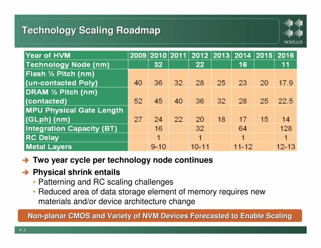
Technology Scaling RoadmapTechnology Scaling Roadmap
� Two year cycle per technology node continues
� Physical shrink entails• Patterning and RC scaling challenges• Reduced area of data storage element of memory requires new
materials and/or device architecture change
NonNon--planar CMOS and Variety of NVM Devices Forecasted to Enable Scalplanar CMOS and Variety of NVM Devices Forecasted to Enable Scaling ing
P. P. 44
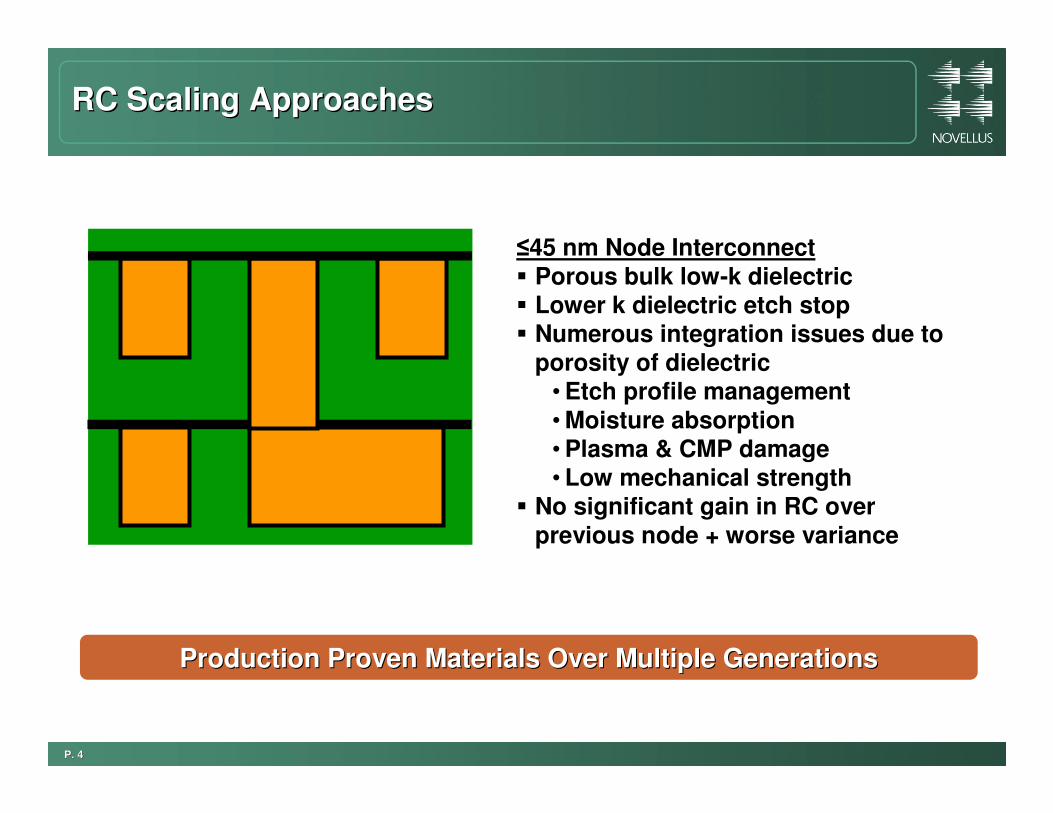
≤45 nm Node Interconnect
� Porous bulk low-k dielectric� Lower k dielectric etch stop� Numerous integration issues due to
porosity of dielectric• Etch profile management
• Moisture absorption• Plasma & CMP damage• Low mechanical strength
� No significant gain in RC over
previous node + worse variance
RC Scaling ApproachesRC Scaling Approaches
Production Proven Materials Over Multiple GenerationsProduction Proven Materials Over Multiple Generations

P. P. 55
RC Scaling ApproachesRC Scaling Approaches
90 nm – 65 nm Node Interconnect� Dense bulk low-k dielectric� Stable dielectric etch stop
� Robust integration with small variance� 20-22% gain in RC over previous node
Production Proven Materials Over Multiple GenerationsProduction Proven Materials Over Multiple GenerationsMany Challenges in Integration of Porous ULKMany Challenges in Integration of Porous ULK
Only Incremental Gain in RCOnly Incremental Gain in RC

P. P. 66 Source: ITRS
Effect of Scattering on RC DelayEffect of Scattering on RC Delay
� Scattering of charge carriers causes > 3X increase in RC• Effective k is a secondary contributor to RC delay
0
5
10
15
20
25
45 32 22 16
Technology Node
RC
(N
orm
ali
ze
d t
o 4
5 n
m n
od
e)
RC with
Scattering
RC without Scattering
Node 65 45 32 22 16
Keff 3.3 2.9 2.8 2.5 2.3
Kbulk 3.1 2.7 2.5 2.2 2.0
Ideal Scaled
RC
Scaled RC delay is dominated by scatteringScaled RC delay is dominated by scattering

P. P. 77
Historical Trends for ITRS LowHistorical Trends for ITRS Low--k Adaptationk Adaptation
� Adaptation of ultra low-k (ULK) films proven harder than anticipated• Roadmap was unrealistic
� Very limited adaptation of ULK with k ≤ 2.5 with hardly any effect on keff
Source: ITRS

P. P. 88
The Case for High Aspect Ratio Metal LinesThe Case for High Aspect Ratio Metal Lines
� “Increasing metal aspect ratio improves RC delay”• M.T. Bohr, Proc. IEEE IEDM, pp. 241-244 (1995)
∆ ∆ ∆ ∆ Scaled (RC) decreases linearly with metal aspect ratioJ. H.-C. Chen, L. Jiang, A. Deutsch, M.A. Angyal and T.A. Spooner, AMC 2008, pp.83–90 (2009)
� Significant improvement in RC with high aspect ratio metal lines• Further enhanced in small dimensions as scattering affects Cu resistivity
• Higher aspect ratio allows higher volume to surface ratio and less scattering

P. P. 99
Meet RC Roadmap With the Same ULK MaterialMeet RC Roadmap With the Same ULK Material
ITRS, benchmark with k scalingVia AR 1.5:1, Metal AR 1.8:1
ITRS, constant keff 2.8
constant keff = 2.8
Metal Aspect Ratio = 3:1, Via Aspect Ratio = 2:1
ITRS, constant keff = 2.5
0
5
10
15
20
25
30
45 32 22 16
Technology Node
RC
(N
orm
alized
to
45 n
m n
od
e)
Approach leads to 30 % Lower RC at 16 nm without changing bulk kApproach leads to 30 % Lower RC at 16 nm without changing bulk k
Source: ITRS & Novellus simulations

P. P. 1010
RC Scaling Approaches RC Scaling Approaches –– A Second LookA Second Look
AR1.8
AR3.0
Scaling Feature Size & Bulk k Alternate Approach

P. P. 1111
RC Scaling Approaches RC Scaling Approaches –– A Second LookA Second Look
High AR Trenches & High AR Trenches & ViasVias in a robust ULK to Enable Lower RCin a robust ULK to Enable Lower RC
≤45 nm Node RC Scaling Approach� A robust ULK material with k = 2.5
• Vertical etch profile
• No moisture absorption• Resistance to plasma damage
� Thin dielectric etch stop� Enable Cu electroplating of high AR
trenches and vias with continuous Cu seed� Improvement in RC
Alternate Approach

P. P. 1212
Porogen-based ULK Dense ULKEtch flaring
Voids with long queue time
65 nm Technology Node
A Dense ULKA Dense ULK
Porogen-basedDense
RC Delay
CureCure
Si
O
SiOSi
O
Si
O
CH3O
Si O CH3
OCH3
CH2
CH3
H3C
O
Si
O
SiOSi
O
Si
O
CH3O
Si O CH3
OCH3
CH2
CH3
H3C
O
Si
O
SiOSi
O
Si
O
CH3O
Si O CH3
OCH3
R
CH3
H3C
O
R
Si
O
SiOSi
O
Si
O
CH3O
Si O CH3
OCH3
R
CH3
H3C
O
R
Dense ULK
Single Precursor
CureCure
Si
O
SiO
SiOSi
O
Si
O
CH3O
Si OCH3
O
OCH3
O
CH3O
H3C
O
H3CSi
O
SiO
SiOSi
O
Si
O
CH3O
Si OCH3
O
OCH3
O
CH3O
H3C
O
H3CSi
O
SiO
SiOSi
O
Si
O
CH3O
Si OCH2
O
OO
O
CH3O
H3C
O
H3CSi
Si
Si
O
SiO
SiOSi
O
Si
O
CH3O
Si OCH2
O
OO
O
CH3O
H3C
O
H3CSi
Si
Porogen-based ULK
Precursor + Porogen
0
1000
1800
Dielectric constant (k)
Solvent Diffusion Coefficient
Porogen-based ULK
Dense ULK
2.5 2.6 2.7 2.8
Dif
f. C
oe
f. o
f IP
A (
um
2/m
in)
Source: Novellus Systems
PALS porosity data
0.5 1.5 2.5Spherical Pore Diameter (nm)
Arb
itra
ry u
nit
s
0 1.0 2.0
Porogen-based
Dense
0.5 1.5 2.5Spherical Pore Diameter (nm)
Arb
itra
ry u
nit
s
0 1.0 2.0
Porogen-based
Dense
Porogen-based
Dense

P. P. 1313
Chemical Structure of Dense ULKChemical Structure of Dense ULK
� D group decreases after UV curing
� Si-CH2-Si group appears after UV curing
� D group decreases after UV curing
� Si-CH2-Si group appears after UV curing
0
0.02
0.04
0.06
0.08
0.1
1225 1275 1325 1375 1425
Wavenumber (cm-1)
Ab
so
rban
ce (
a.u
.)
AS DEP
UV Cured
DD
Si-CH2-Si
TT
DD
TT
CH3
O
CH3
OSi
CH3
O
O
OSi
Composition from RBS & HFSSi:O:H:C = 0.14:0.21:0.32:0.33
A Ratio of peak area
Parameter Technique Units Dense ULKSi-CH3/Si-O A FTIR % 3.5 ± 0.2
CHx/Si-O A FTIR % 3.2 ± 0.2

P. P. 1414
Fundamental Studies of ULK Etch ProcessFundamental Studies of ULK Etch ProcessMeasurements of Etching YieldMeasurements of Etching Yield
0
200
400
600
800
1000
0 15 30 45 60 75 90Off-normal Angle( o)
Etc
hing
Yie
ld (
Å/1
017
ions
)
Dense ULK
SiO2Coral
Porogen-based ULK
� Process conditions:• RF 400 W, DC 350 V• 7% C4F8/Ar• Beam source pressure: 4mT
Sample in cryopumped
lower chamber
e-
Filament for Beam Space
Charge Neutralization
Gridded Orifice,
Grounded
Extracted Plasma Beam
Plasma 0 – 500 V
Ceramic Liner
θθθθ
Experimental Etch Studies ����(H.H. Sawin/W. Guo MIT)
Source: G. A. Antonelli, G. Jiang, M. Sriram, K. Chattopadhyay, W. Guo, and H.H. Sawin, Mat. Res. Soc. Symp. Proc. 1249, F04-15 (2010)

P. P. 1515
Fundamental Studies of ULK Etch ProcessFundamental Studies of ULK Etch ProcessPostPost--Etch Surface CompositionEtch Surface Composition
0
200
400
600
800
1000
0 15 30 45 60 75 90Off-normal Angle(o)
Etc
hing
Yie
ld (
Å/1
017
ions
)
Dense ULK
SiO2Coral
Porogen-based ULK
How do we explain this result?
High carbon and fluorine levels at the surface suggest polymer formation
0
0.2
0.4
0.6
0.8
Su
rfac
e C
om
po
sit
ion
Fra
cti
on
0 30 60 90Off-normal Angle(°)
Si O F C
0
0.2
0.4
0.6
0.8
Off-normal Angle(°)
0 30 60 90
Si O F C
Su
rfac
e C
om
po
sit
ion
Fra
cti
on
XPS Studies of Surface Composition
Porogen-Based ULK
Dense ULK
Source: G. A. Antonelli, G. Jiang, M. Sriram, K. Chattopadhyay, W. Guo, and H.H. Sawin, Mat. Res. Soc. Symp. Proc. 1249, F04-15 (2010)

P. P. 1616
Line Edge Roughness and the ULK Etch ProcessLine Edge Roughness and the ULK Etch Process
82o off-normal angle C4F8/Ar Plasma
75o off-normal angle C4F8/Ar Plasma
RMS = 1.1 nm RMS = 1.8 nm RMS = 2.8 nm
RMS = 1.4 nm RMS = 4.5 nm RMS = 12.5 nm
High Si-CH3Non-Optimized Si-CH3Optimized Si-CH3
Optimized cure conditions result in improved sidewall roughness
Source: G. A. Antonelli, G. Jiang, M. Sriram, K. Chattopadhyay, W. Guo, and H.H. Sawin, Mat. Res. Soc. Symp. Proc. 1249, F04-15 (2010)

P. P. 1717
Coral
154.5nm
83.2nm114.9 nm
Porogen-based ULK
108.8nm
158.5nm
84.6nm
Dense ULK
81.7nm
154.7nm
108.7nm
Novellus SystemsCustomer Integration Center
Fundamental Studies of ULK Etch ProcessFundamental Studies of ULK Etch ProcessComparison of 65 nm Node Features in LowComparison of 65 nm Node Features in Low--k & ULK Materialsk & ULK Materials
Source: G. A. Antonelli, G. Jiang, M. Sriram, K. Chattopadhyay, W. Guo, and H.H. Sawin, Mat. Res. Soc. Symp. Proc. 1249, F04-15 (2010)
Etched in Lam Research system with CF4/Ar/O2 gas mixture
Off-normal Angle( )
0
200
400
600
800
1000
0 15 30 45 60 75 90o
Etc
hing
Yie
ld (
Å/1
017
ions
)
Dense ULK
SiO2Coral
Porogen-based ULK

P. P. 1818
IBM 32 nm Node Features in Dense ULKIBM 32 nm Node Features in Dense ULKProcess Flow & CrossProcess Flow & Cross--SectionsSections
Process Flow STEM of Trench Features:
Source: IBM
Dep. dielectric barrier
Dep. dense ULK
Dep. HM stack
Spin on organic layer
Via litho & etch
Trench litho & etch
Dep. Barrier & Cu Seed
Electroplate Cu
Cu Anneal
Cu CMP
planarizing layer

P. P. 1919
150oC Comb-Serp I-V Plot: 8SJB6
1.E-14
1.E-13
1.E-12
1.E-11
1.E-10
1.E-09
1.E-08
1.E-07
1.E-06
1.E-05
1.E-04
1.E-03
1.E-02
0 10 20 30 40 50 60 70
Voltage (volts)
Cu
rren
t (a
mp
s)
Patterned wafer level stress breakdown results:
Stress Charge
1.E+10
1.E+11
1.E+12
1.E+13
1.E+14
1.E+15
1.E+16
1.E+17
1.E+18
1 3 5 7 9 11 13 15 17 19 21 23
Site Number
Ch
arg
e
8SJB6
2 Stress Fails
Test conditions:3 MV/cm stress for 3 minutes prior to each I-V.
Current measured and integrated into a charge during stress.
Stress Fails
Source: IBM
IBM 32 nm Node Features in Dense ULKIBM 32 nm Node Features in Dense ULKPreliminary Reliability ResultsPreliminary Reliability Results
Module level TDDB results:
TD
DB
Failu
re P
rob
ab
ilit
y (
%)
Failure Time (h)
1E-3 0.01 0.1 1 10 100 10001
10
40
70
95
no fails 14.5V(3.5Mv/cm)
477h
M2 areatddb_1A 1cmps1 pads 18,20space 41nm
16.5V (4.0 MV/cm)18.5V (4.5 MV/cm)20.5V (5.0 MV/cm)
TD
DB
Failu
re P
rob
ab
ilit
y (
%)
Failure Time (h)
1E-3 0.01 0.1 1 10 100 10001
10
40
70
95
no fails 14.5V(3.5Mv/cm)
477h
M2 area tddb_1A 1cmps1 pads 18,20space 41nm
16.5V (4.0 MV/cm)18.5V (4.5 MV/cm)20.5V (5.0 MV/cm)

P. P. 2020 Source: IBM
EDX Analysis of ALD Compatibility of Dense ULKEDX Analysis of ALD Compatibility of Dense ULK
No Ta diffusion into the dense ULK was observed
EDX:STEM:
(Red color indicates presence of Ta)

P. P. 2121
Position (nm)
C/O
C/O
C/O
Position (nm)
EELS Analysis of Process Damage in Dense ULKEELS Analysis of Process Damage in Dense ULK
Source: IBM
EELS:

P. P. 2222
IBM 22 nm Node Features in Dense ULKIBM 22 nm Node Features in Dense ULKPerformance of Interconnects with Higher Aspect Ratio TrenchPerformance of Interconnects with Higher Aspect Ratio Trench
A reduction in resistance is observed at higher trench aspect raA reduction in resistance is observed at higher trench aspect ratio tio
Source: IBM
Trench
Aspect Ratio
Resistance Shift
(40 nm line width)
Resistance Shift
(80 nm line width)
2.15:1 -14% -14%
2.33:1 -14% -23%

P. P. 2323
Challenges for PVD Cu Extendibility to <22nmChallenges for PVD Cu Extendibility to <22nm
� Seed overhang• Critical due to small top opening
� Sidewall coverage• Limited due to overhang growth
� Edge asymmetry• Critical with thinner sidewall coverage
� Pre-plate aspect ratio• Becomes higher after B/S relative to larger feature
M1 & M2 Copper
Barrier/Seed
Small geometries test PVD Cu extendibilitySmall geometries test PVD Cu extendibility

P. P. 2424
Hollow Cathode Magnetron Advanced Cu SeedHollow Cathode Magnetron Advanced Cu Seed
1. Cu deposited at a high density plasma
2. Cu migrates to lower surface energy state
Cu Neutral
Cu+ Ion
PVD Cu seed only
PVD Cu seed & Electroplated Cu
Source: Novellus Systems
PVD Cu seed only

P. P. 2525
ConclusionsConclusions
� How can we resolve the ITRS “Difficult Challenge” of RC, filling small features, and reliability with robust integrated suite of processes?
� This data indicates that one possible solution could be shifting scaling to trench and via aspect ratio
� That transition is predicated on having a robust ULK material capable of being patterned at such aspect ratios and the ability to fill these features with copper
� Dense ULK materials designed to have a low pore interconnectivity and a high carbon content can meet these patterning requirements, have a low susceptibility to process induced damage, and are compatible with future metal barrier deposition technologies
� When necessary, alternate methods of copper seed deposition exist and could be used to further extend electrochemical fill methods