last lect metallization 2014
DESCRIPTION
metalization lectureTRANSCRIPT
Anshuman Dalvi
Dr Dalvi Lectures, IC Fab tech. 20141
Metallization
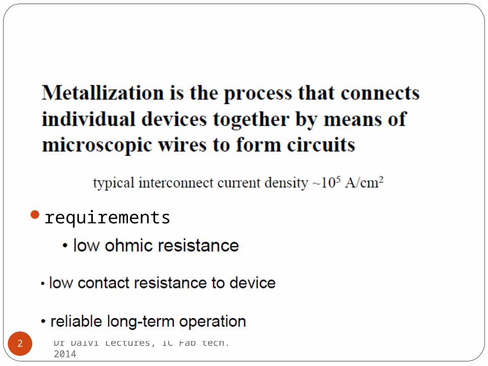
Dr Dalvi Lectures, IC Fab tech. 20142
requirements
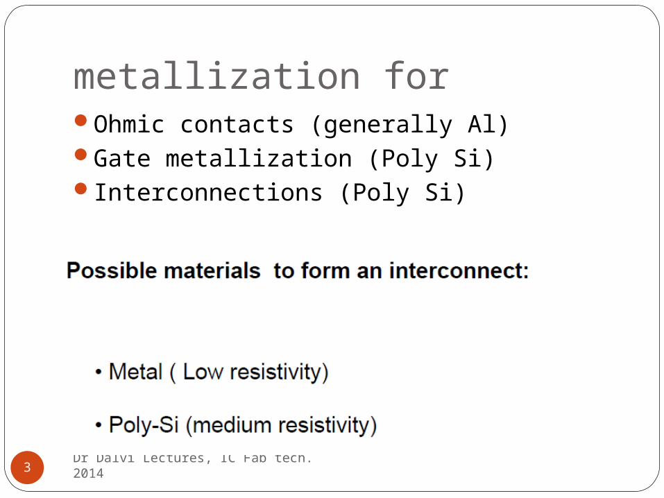
metallization for
Dr Dalvi Lectures, IC Fab tech. 20143
Ohmic contacts (generally Al)Gate metallization (Poly Si)Interconnections (Poly Si)
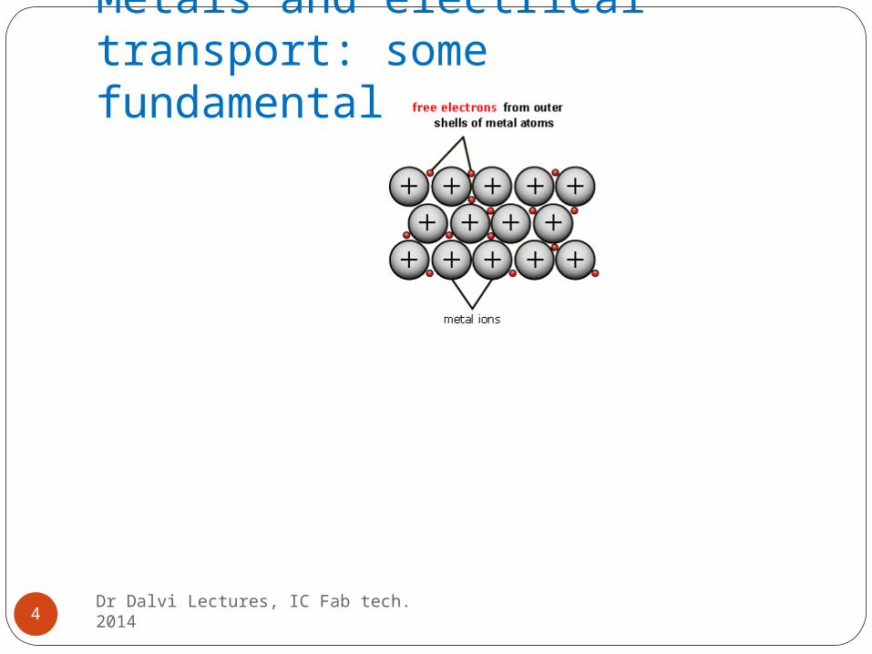
Metals and electrical transport: some fundamentals
Dr Dalvi Lectures, IC Fab tech. 20144
Electrical conductivity in metals
Dr Dalvi Lectures, IC Fab tech. 20145
Matthiessen's Rule
Dr Dalvi Lectures, IC Fab tech. 20146
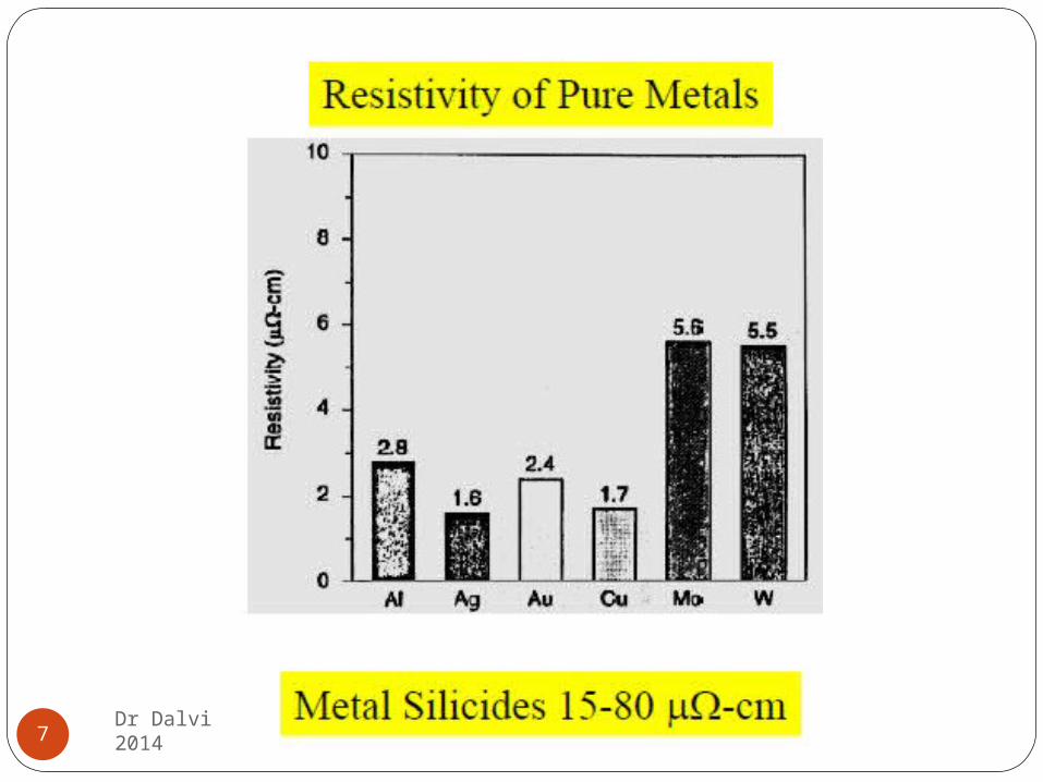
Dr Dalvi Lectures, IC Fab tech. 20147
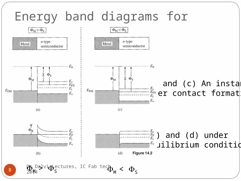
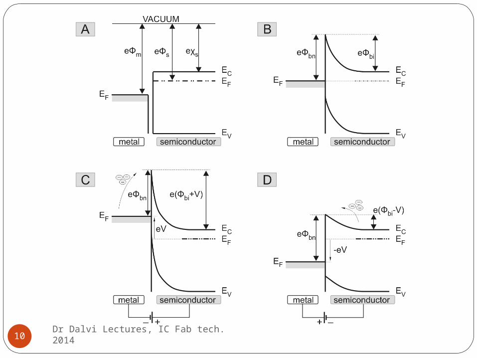
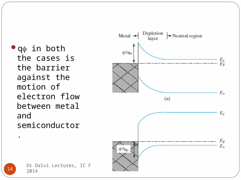
Energy band diagrams for ideal MS contacts
Dr Dalvi Lectures, IC Fab tech. 20148 M > S M < S
(a) and (c) An instant after contact formation
(b) and (d) underequilibrium conditions
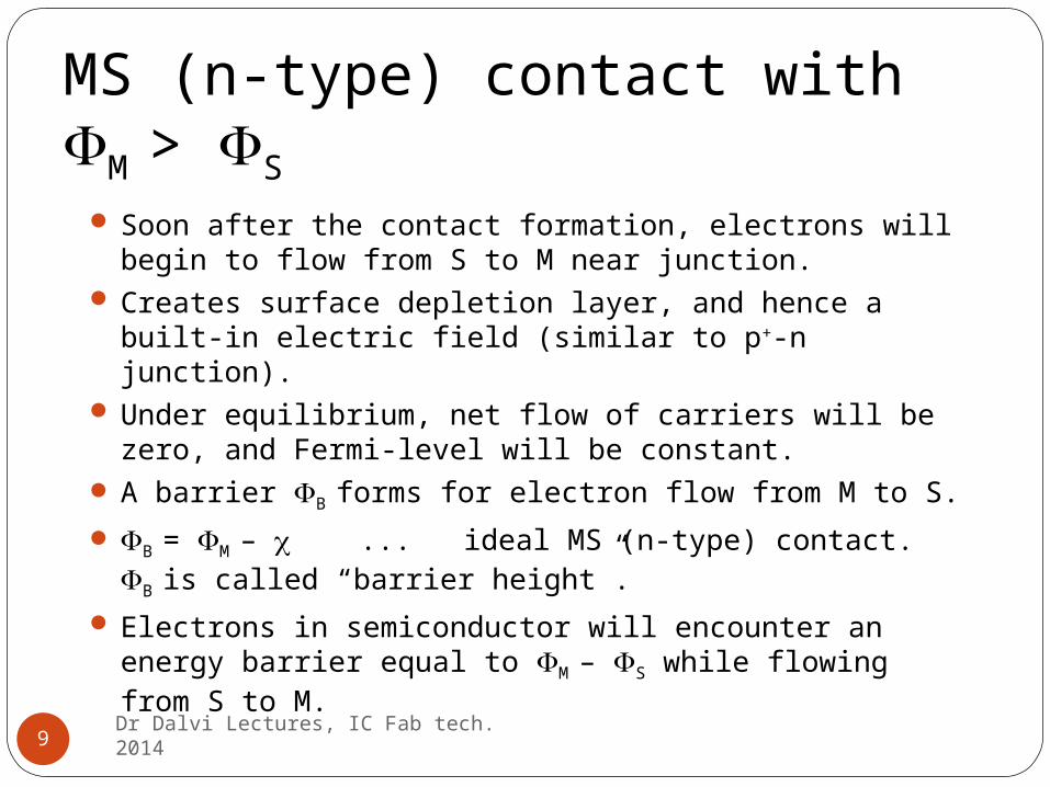
MS (n-type) contact with M > S
Dr Dalvi Lectures, IC Fab tech. 20149
Soon after the contact formation, electrons will begin to flow from S to M near junction.
Creates surface depletion layer, and hence a built-in electric field (similar to p+-n junction).
Under equilibrium, net flow of carriers will be zero, and Fermi-level will be constant.
A barrier B forms for electron flow from M to S.
B = M – ... ideal MS (n-type) contact. B is called “barrier height”.
Electrons in semiconductor will encounter an energy barrier equal to M – S while flowing from S to M.
Dr Dalvi Lectures, IC Fab tech. 201410
Dr Dalvi Lectures, IC Fab tech. 201411
Dr Dalvi Lectures, IC Fab tech. 201412
Dr Dalvi Lectures, IC Fab tech. 201413
Dr Dalvi Lectures, IC Fab tech. 201414
q in both the cases is the barrier against the motion of electron flow between metal and semiconductor.
Dr Dalvi Lectures, IC Fab tech. 201415
Dr Dalvi Lectures, IC Fab tech. 201416
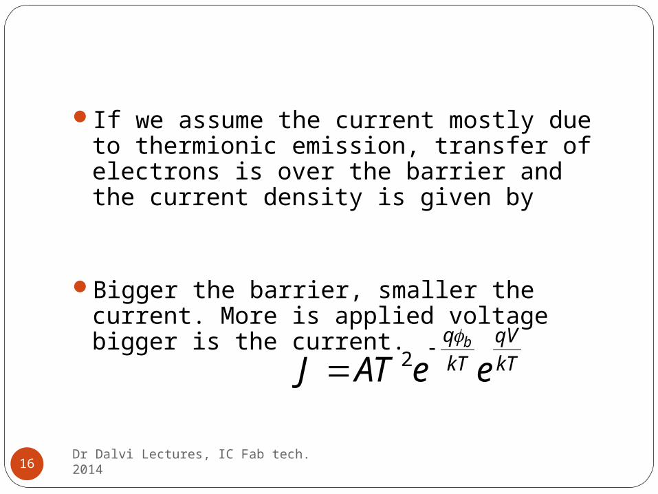
If we assume the current mostly due to thermionic emission, transfer of electrons is over the barrier and the current density is given by
Bigger the barrier, smaller the current. More is applied voltage bigger is the current.
kT
qV
kT
q
eeATJb
2
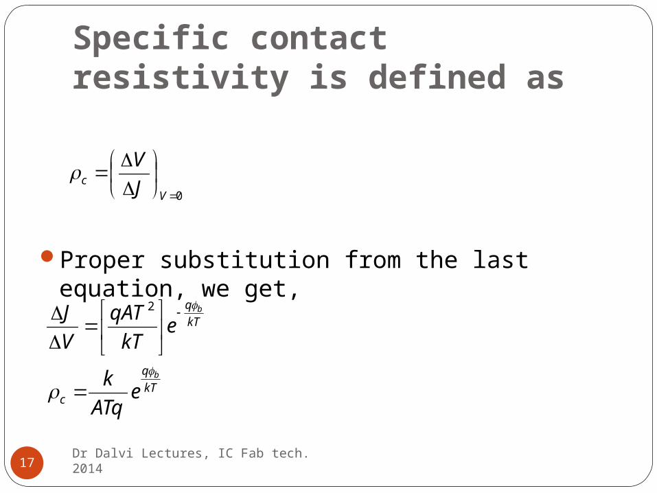
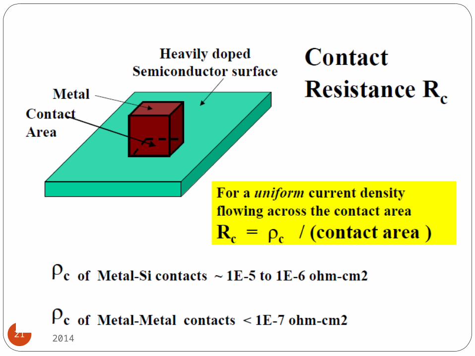
Specific contact resistivity is defined as
Dr Dalvi Lectures, IC Fab tech. 201417
Proper substitution from the last equation, we get,
0
V
c J
V
kT
q
c
kT
q
b
b
eATq
k
ekT
qAT
V
J
2
Dr Dalvi Lectures, IC Fab tech. 201418
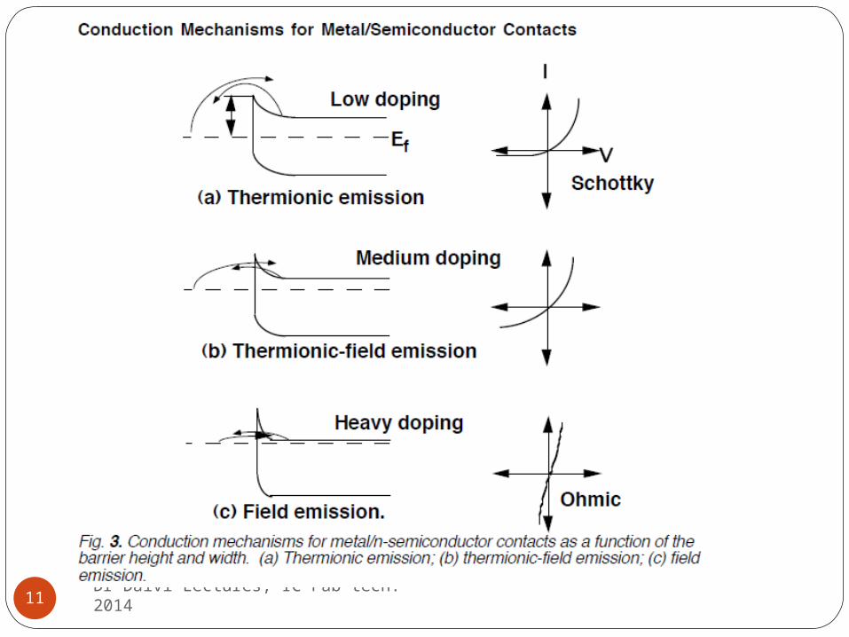
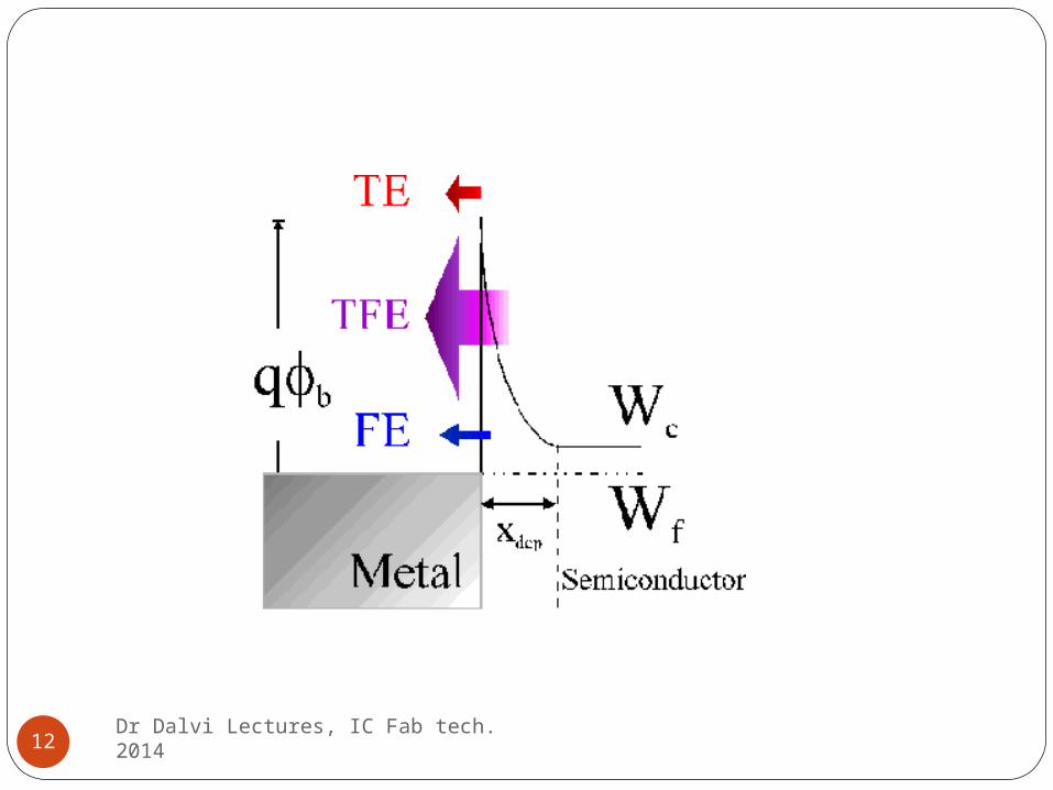
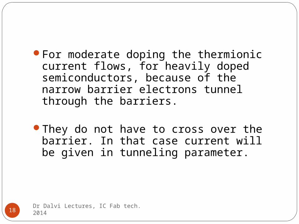
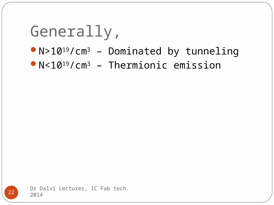
For moderate doping the thermionic current flows, for heavily doped semiconductors, because of the narrow barrier electrons tunnel through the barriers.
They do not have to cross over the barrier. In that case current will be given in tunneling parameter.
Dr Dalvi Lectures, IC Fab tech. 201419
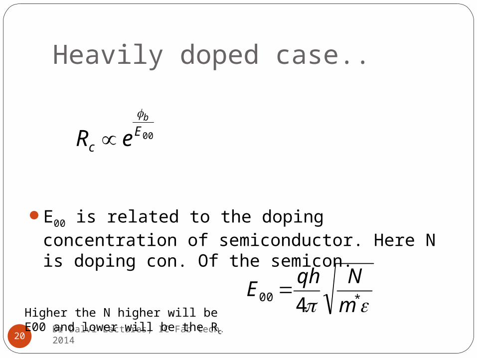
Heavily doped case..
Dr Dalvi Lectures, IC Fab tech. 201420
E00 is related to the doping concentration of semiconductor. Here N is doping con. Of the semicon.
Higher the N higher will be E00 and lower will be the Rc
00Ec
b
eR
*00 4 m
NqhE
Dr Dalvi Lectures, IC Fab tech. 201421
Generally,
Dr Dalvi Lectures, IC Fab tech. 201422
N>1019/cm3 – Dominated by tunnelingN<1019/cm3 – Thermionic emission
Dr Dalvi Lectures, IC Fab tech. 201423
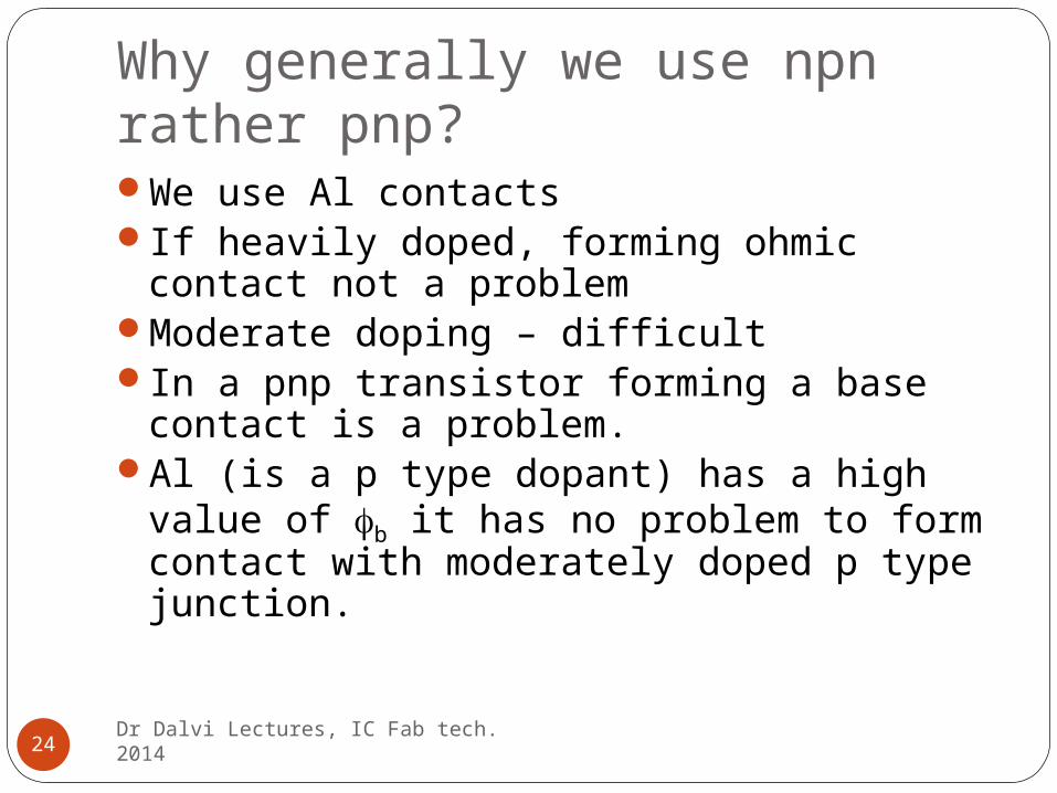
Why generally we use npn rather pnp?
Dr Dalvi Lectures, IC Fab tech. 201424
We use Al contactsIf heavily doped, forming ohmic contact not
a problemModerate doping – difficultIn a pnp transistor forming a base contact
is a problem.Al (is a p type dopant) has a high value of
b it has no problem to form contact with moderately doped p type junction.
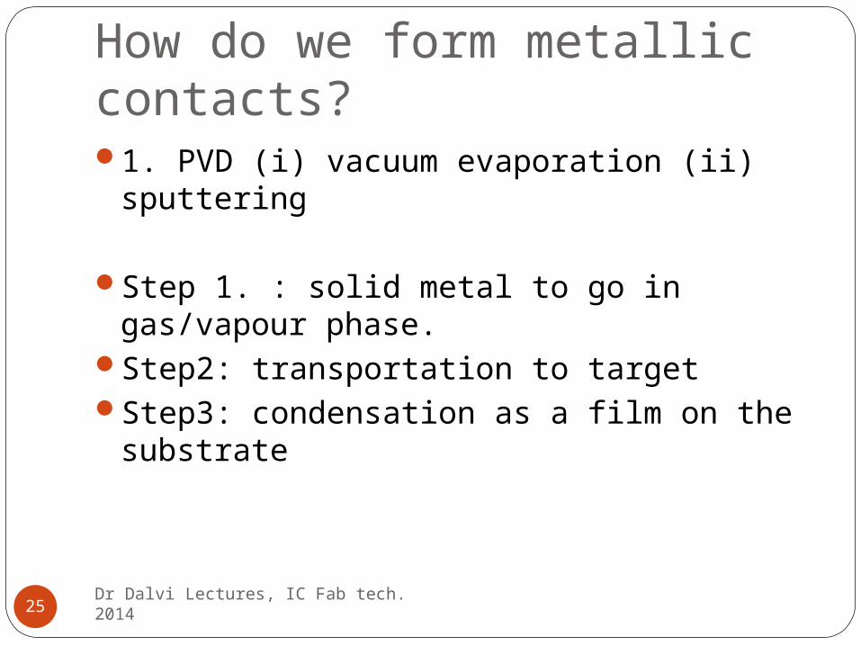
How do we form metallic contacts?
Dr Dalvi Lectures, IC Fab tech. 201425
1. PVD (i) vacuum evaporation (ii) sputtering
Step 1. : solid metal to go in gas/vapour phase.
Step2: transportation to targetStep3: condensation as a film on the
substrate
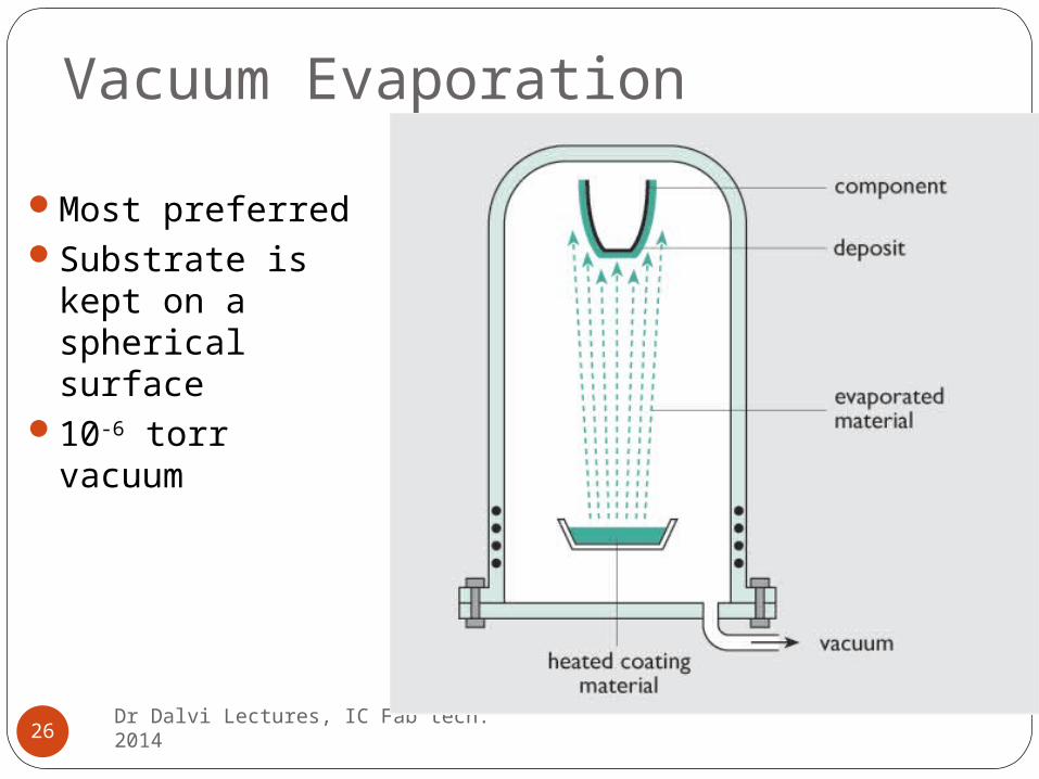
Vacuum Evaporation
Dr Dalvi Lectures, IC Fab tech. 201426
Most preferredSubstrate is kept
on a spherical surface
10-6 torr vacuum
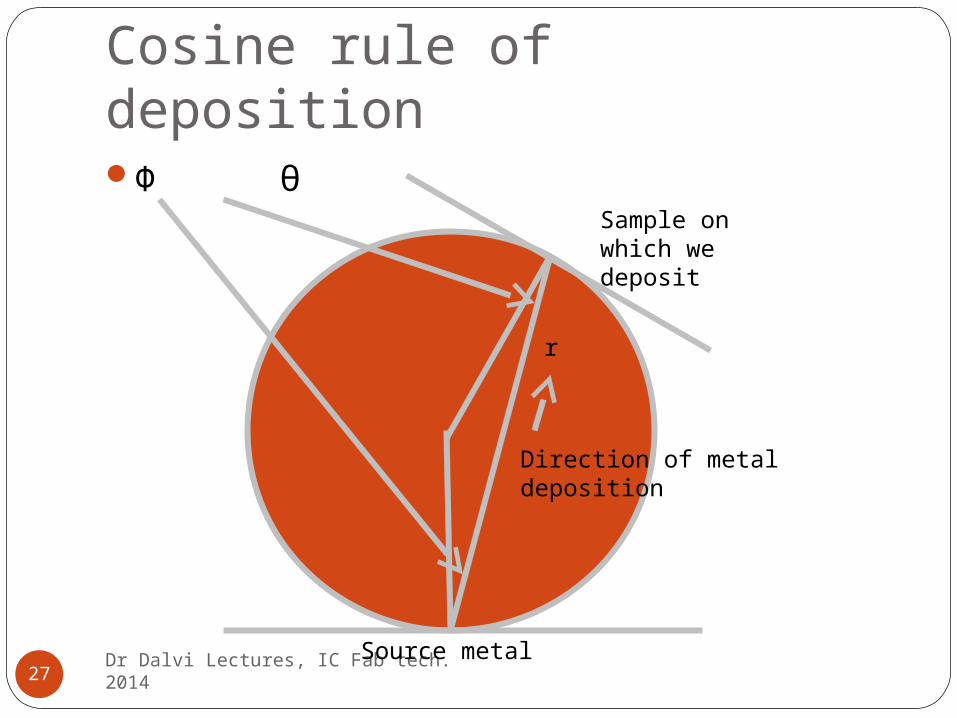
Cosine rule of deposition
Dr Dalvi Lectures, IC Fab tech. 201427
Φ θ
Direction of metal deposition
Sample on which we deposit
Source metal
r
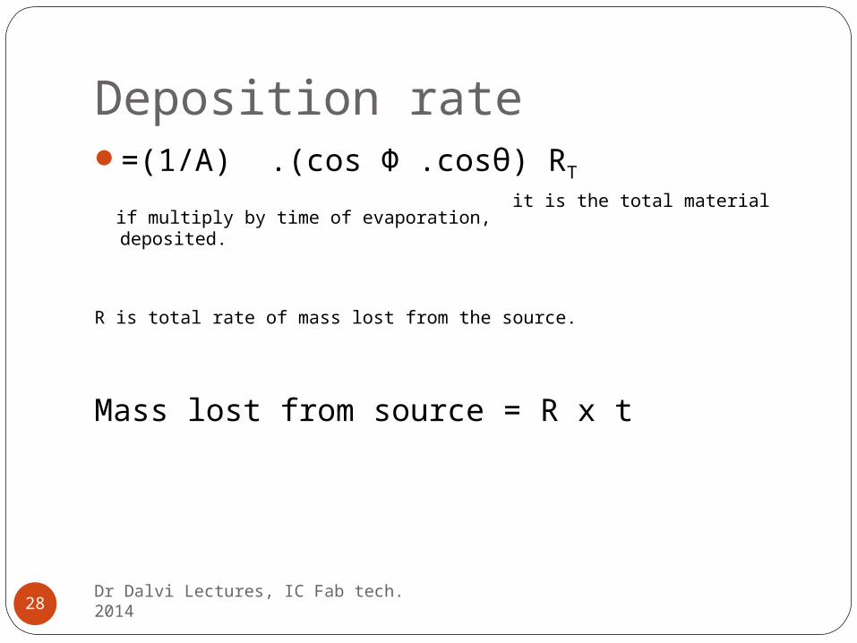
Deposition rate
Dr Dalvi Lectures, IC Fab tech. 201428
=(1/A) .(cos Φ .cosθ) RT
if multiply by time of evaporation, it is the total material deposited.
R is total rate of mass lost from the source.
Mass lost from source = R x t
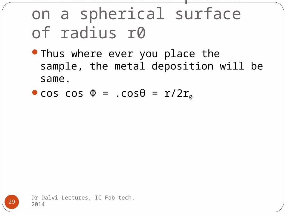
If substrate is placed on a spherical surface of radius r0
Dr Dalvi Lectures, IC Fab tech. 201429
Thus where ever you place the sample, the metal deposition will be same.
cos cos Φ = .cosθ = r/2r0
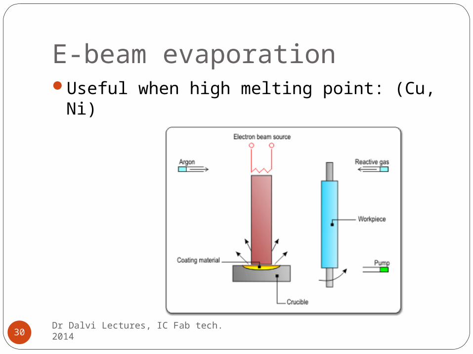
E-beam evaporation
Dr Dalvi Lectures, IC Fab tech. 201430
Useful when high melting point: (Cu, Ni)
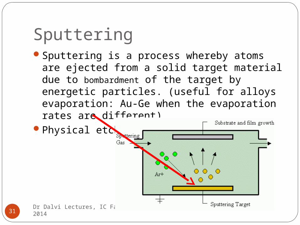
Sputtering
Dr Dalvi Lectures, IC Fab tech. 201431
Sputtering is a process whereby atoms are ejected from a solid target material due to bombardment of the target by energetic particles. (useful for alloys evaporation: Au-Ge when the evaporation rates are different)
Physical etching
Dr Dalvi Lectures, IC Fab tech. 201432
Good thing about sputtering: composition is maintained.
Bad part: damages due to ion beam bombardment.
Some contamination is also likely due to high pressure on the film (films may have trapped gas)
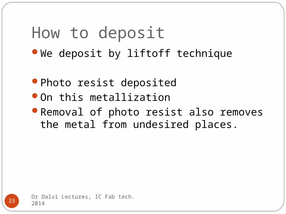
How to deposit
Dr Dalvi Lectures, IC Fab tech. 201433
We deposit by liftoff technique
Photo resist depositedOn this metallizationRemoval of photo resist also removes the
metal from undesired places.
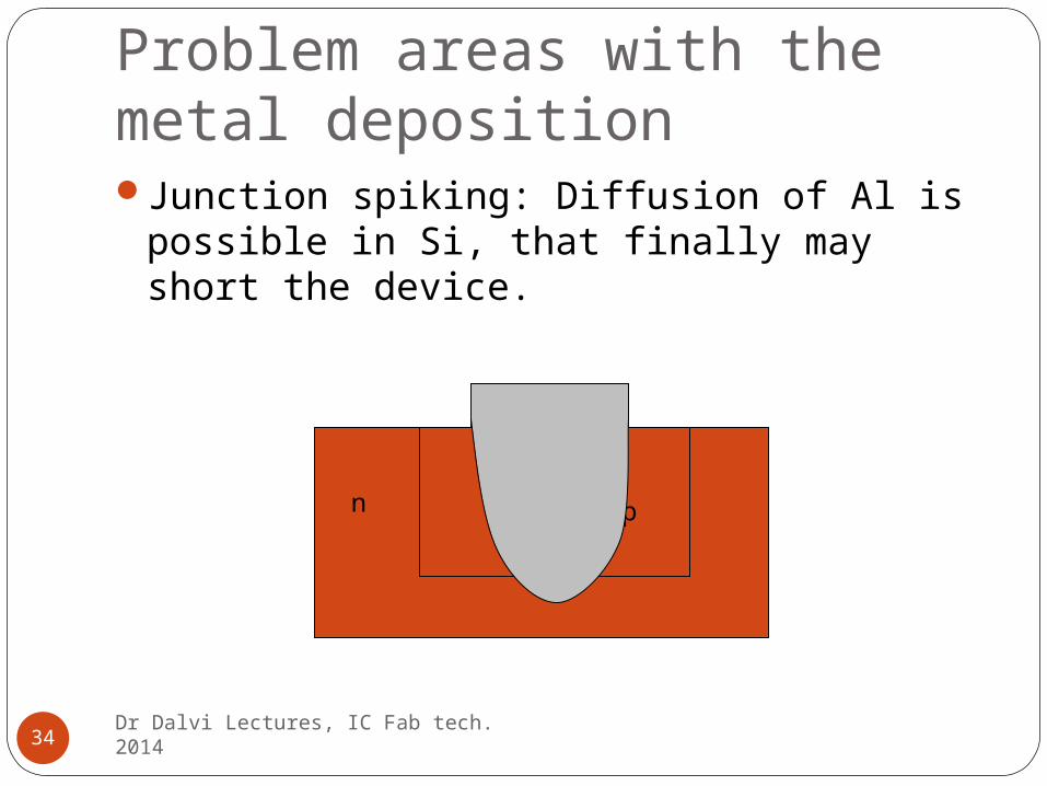
Problem areas with the metal deposition
Dr Dalvi Lectures, IC Fab tech. 201434
Junction spiking: Diffusion of Al is possible in Si, that finally may short the device.
pn

Problem area 2
Dr Dalvi Lectures, IC Fab tech. 201435
Electro migration: Along the direction of the electrical field, metal lines start moving.
Thus we may have break and accumulation of charges.
Problems in Al metal contact: Spiking
Dr Dalvi Lectures, IC Fab tech. 201436
If the dimensions of the window (width and depth) are reduced – big problem
Small window is a problem
Shallow junction is a problem
Dr Dalvi Lectures, IC Fab tech. 201437
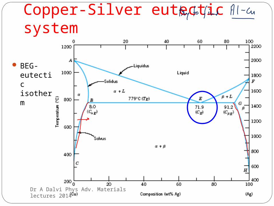
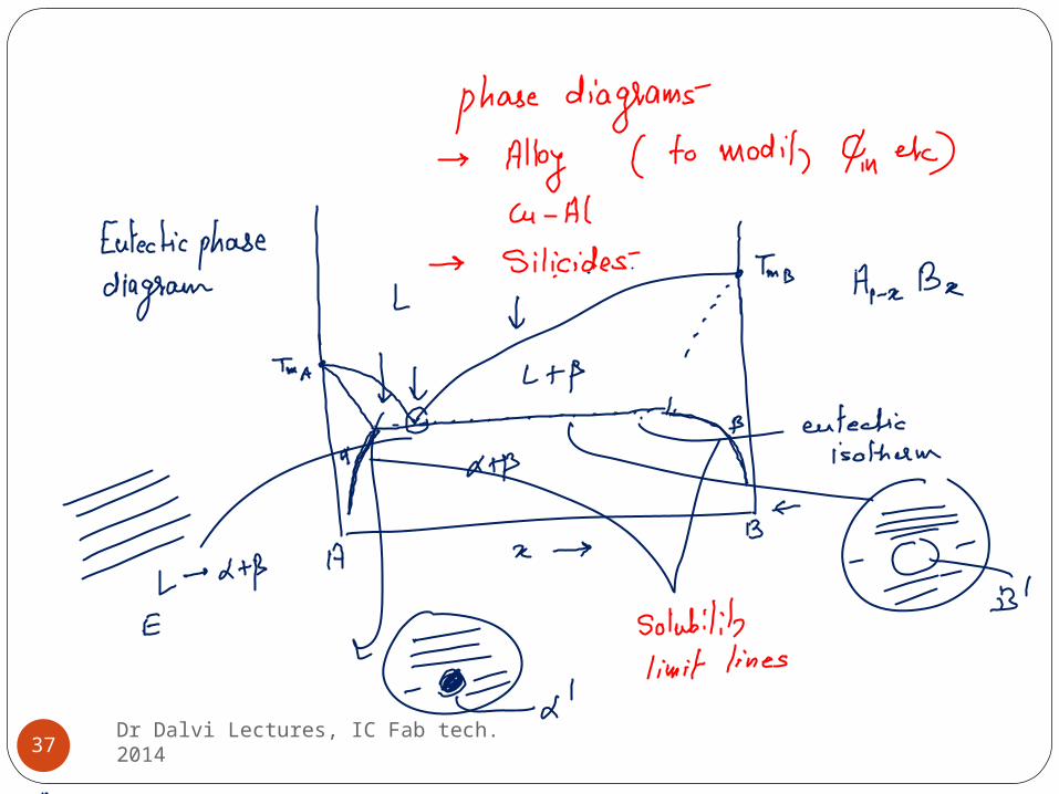
Copper-Silver eutectic system
BEG- eutectic isotherm
Dr A Dalvi Phys Adv. Materials lectures 2014
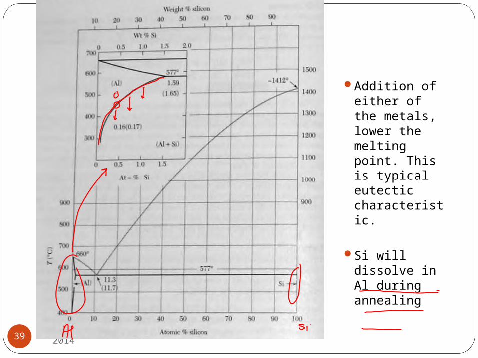
Addition of either of the metals, lower the melting point. This is typical eutectic characteristic.
Si will dissolve in Al during annealing
Dr Dalvi Lectures, IC Fab tech. 201439
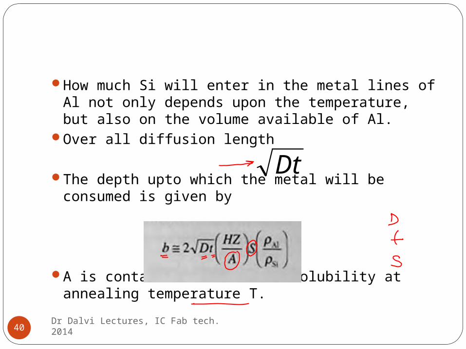
How much Si will enter in the metal lines of Al not only depends upon the temperature, but also on the volume available of Al.
Over all diffusion length
The depth upto which the metal will be consumed is given by
A is contact area and S is solubility at annealing temperature T.
Dr Dalvi Lectures, IC Fab tech. 201440
Dt
Solution: Presence of impurities in Al
Dr Dalvi Lectures, IC Fab tech. 201441
Mix some Si in Al during the depositionIf metal contains some impurity,
diffusion of Si is affected.Con> 1wt% Si in Al should be used.IMP: If access Si is used, it may
precipitate and since it is having Al in it it is becomes a P type Si. Thus we will destroy the ohmic contact by making another pn junction.
This problem will not arise for junction with p type Si.
Dr Dalvi Lectures, IC Fab tech. 201442
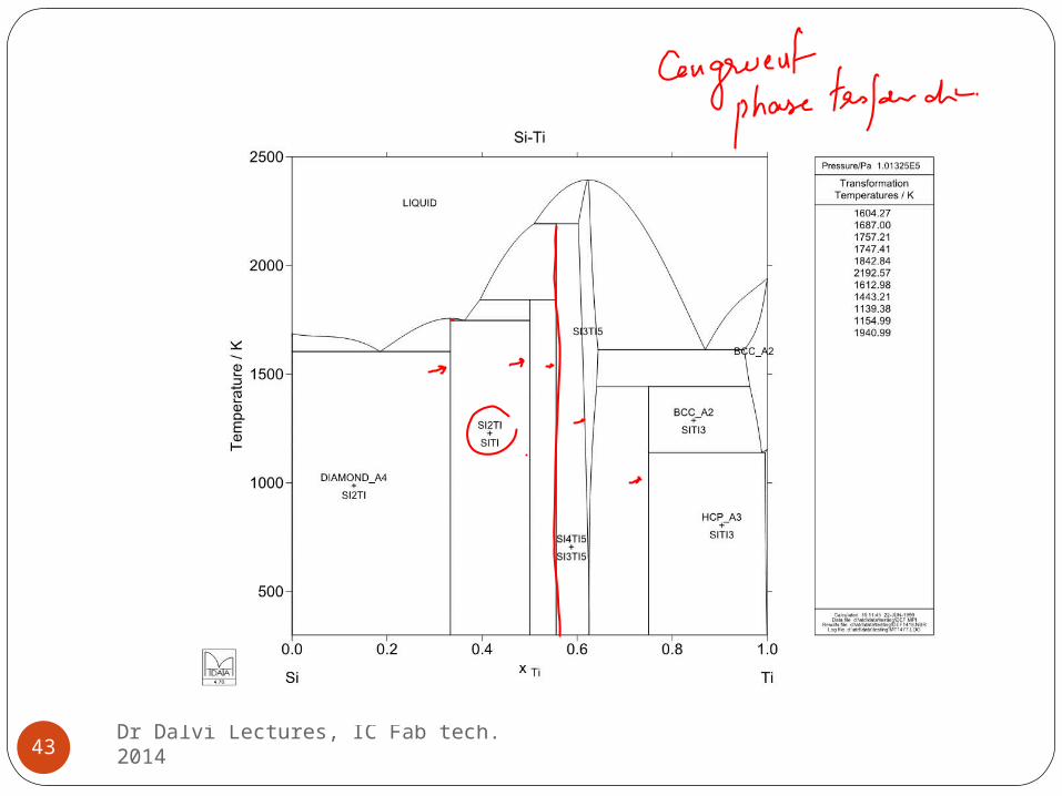
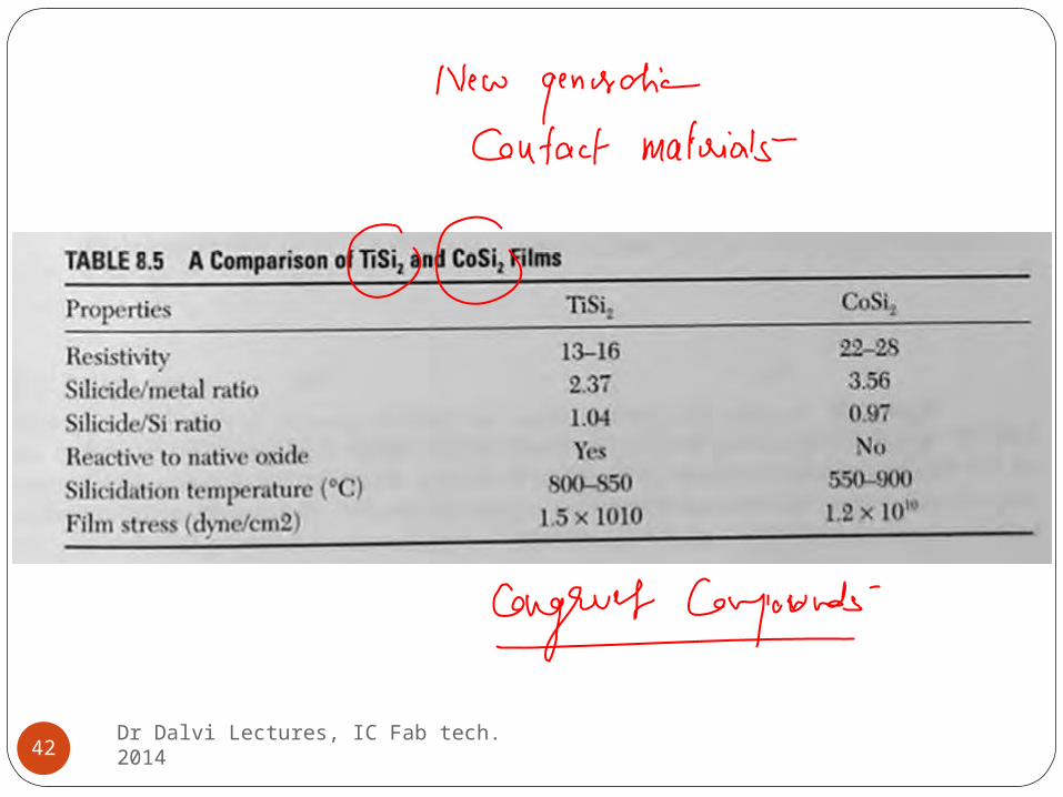
Dr Dalvi Lectures, IC Fab tech. 201443
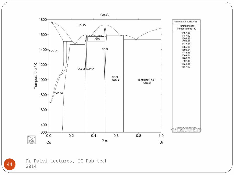
Dr Dalvi Lectures, IC Fab tech. 201444
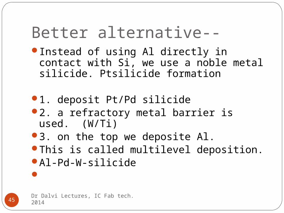
Better alternative--
Dr Dalvi Lectures, IC Fab tech. 201445
Instead of using Al directly in contact with Si, we use a noble metal silicide. Ptsilicide formation
1. deposit Pt/Pd silicide2. a refractory metal barrier is used.
(W/Ti)3. on the top we deposite Al. This is called multilevel deposition.Al-Pd-W-silicide
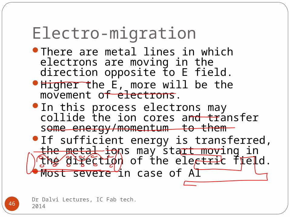
Electro-migration
Dr Dalvi Lectures, IC Fab tech. 201446
There are metal lines in which electrons are moving in the direction opposite to E field.
Higher the E, more will be the movement of electrons.
In this process electrons may collide the ion cores and transfer some energy/momentum to them
If sufficient energy is transferred, the metal ions may start moving in the direction of the electric field.
Most severe in case of Al
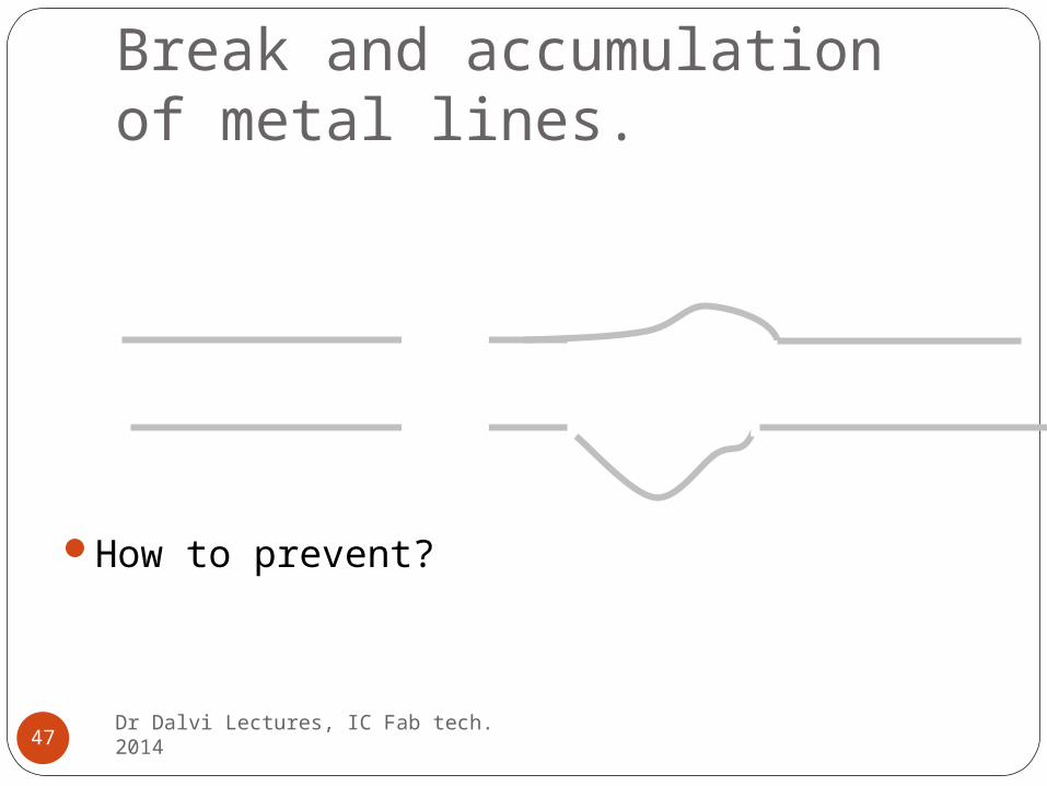
Break and accumulation of metal lines.
Dr Dalvi Lectures, IC Fab tech. 201447
How to prevent?
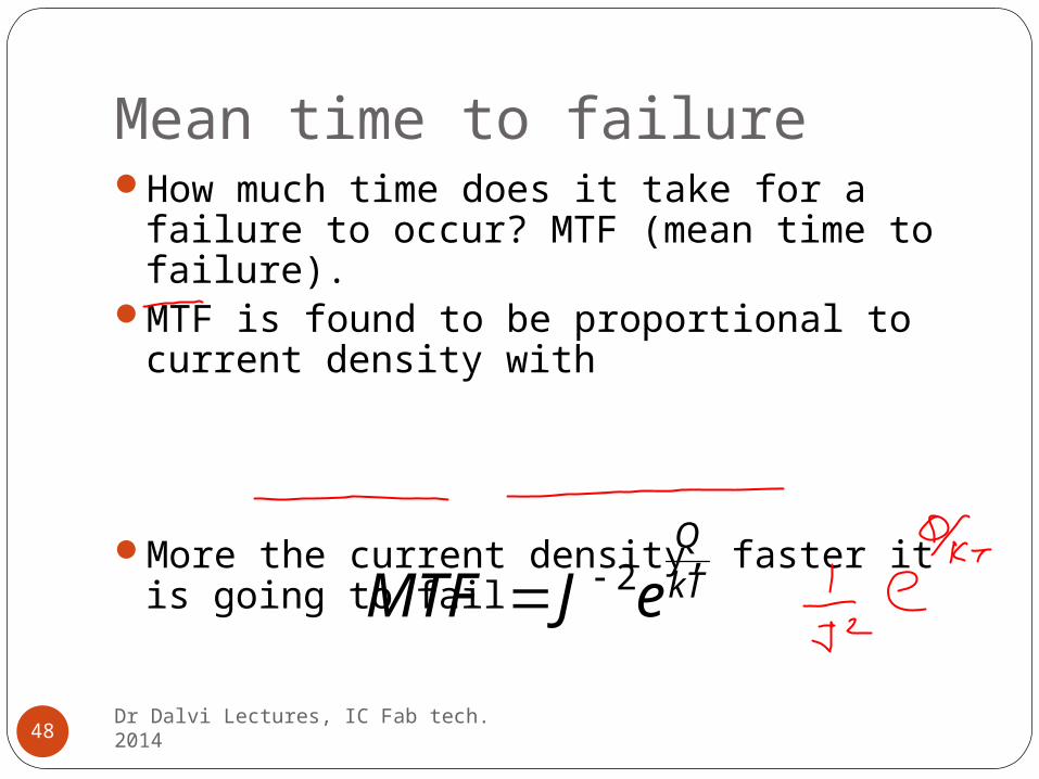
Mean time to failure
Dr Dalvi Lectures, IC Fab tech. 201448
How much time does it take for a failure to occur? MTF (mean time to failure).
MTF is found to be proportional to current density with
More the current density, faster it is going to fail
kT
Q
eJMTF 2
Dr Dalvi Lectures, IC Fab tech. 201449
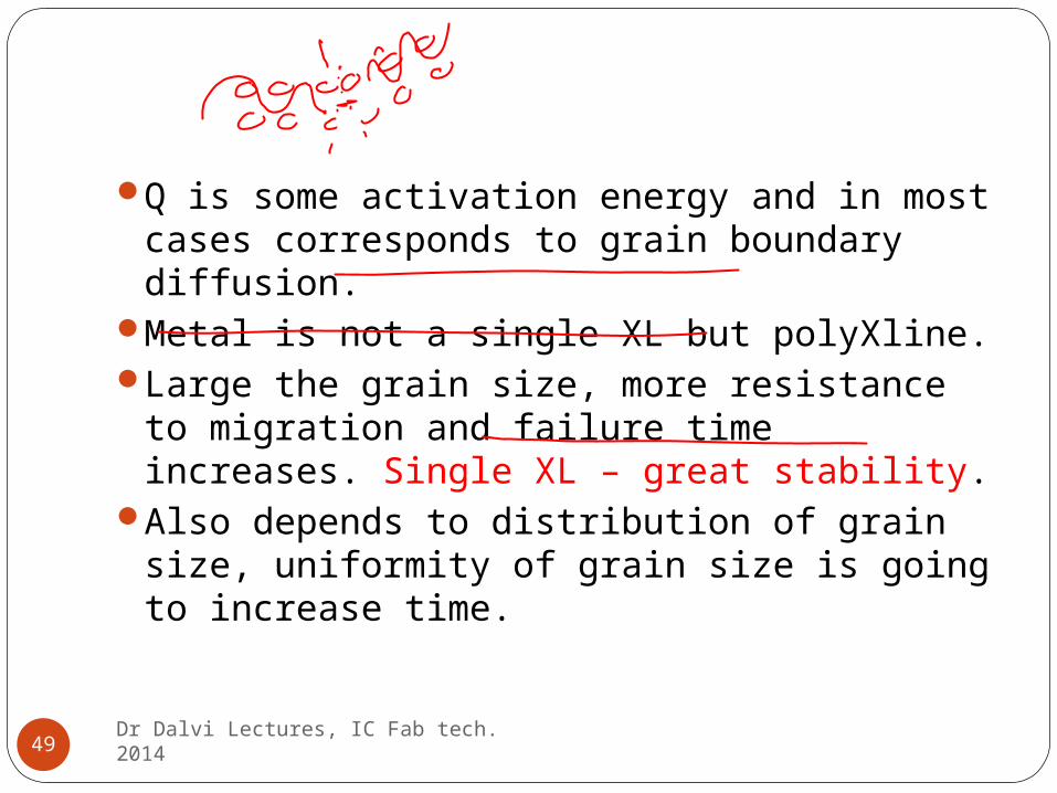
Q is some activation energy and in most cases corresponds to grain boundary diffusion.
Metal is not a single XL but polyXline. Large the grain size, more resistance to
migration and failure time increases. Single XL – great stability.
Also depends to distribution of grain size, uniformity of grain size is going to increase time.
Shrinking of device dimensions helps.
Dr Dalvi Lectures, IC Fab tech. 201450
As the lines become narrow, mean time to failure increases.
Because if line width decreases, Al is going to form single XL layer.
alloy
Dr Dalvi Lectures, IC Fab tech. 201451
Instead of using Al alone, we can use Al-Cu alloy
Addition of copper increases the value of Q and mean time to failure improves.