springerseriesin - cas
TRANSCRIPT


Springer Series in
advanced microelectronics 27

Springer Series in
advanced microelectronicsSeries Editors: K. Itoh T. Lee T. Sakurai W.M.C. Sansen D. Schmitt-Landsiedel
The Springer Series in Advanced Microelectronics provides systematic information onall the topics relevant for the design, processing, and manufacturing of microelectronicdevices. The books, each prepared by leading researchers or engineers in their f ields,cover the basic and advanced aspects of topics such as wafer processing, materials,device design, device technologies, circuit design, VLSI implementation, and subsys-tem technology. The series forms a bridge between physics and engineering and thevolumes will appeal to practicing engineers as well as research scientists.
18 Microcontrollers in PracticeBy I. Susnea and M. Mitescu
19 Gettering Defectsin SemiconductorsBy V.A. Perevoschikov and V.D. Skoupov
20 Low Power VCO Design in CMOSBy M. Tiebout
21 Continuous-Time Sigma-Delta A/D ConversionFundamentals, Performance Limits and Robust ImplementationsBy M. Ortmanns and F. Gerfers
22 Detection and Signal ProcessingTechnical RealizationBy W.J. Witteman
23 Highly Sensitive Optical ReceiversBy K. Schneider and H.K. Zimmermann
24 Bonding in Microsystem TechnologyBy J.A. Dziuban
25 Power Management of Digital Circuits in Deep Sub-Micron CMOS TechnologiesBy S. Henzler
26 High-Dynamic-Range (HDR) VisionMicroelectronics, Image Processing, Computer GraphicsEditor: B. Hoefflinger
27 Advanced Gate Stacks for High-Mobility SemiconductorsEditors: A. Dimoulas, E. Gusev, P.C. McIntyre, and M. Heyns
Volumes 1–17 are listed at the end of the book.

A. Dimoulas E. GusevP.C. McIntyre M. Heyns(Eds.)
Advanced Gate Stacksfor High-MobilitySemiconductors
123
With 292 Figures

Dr. Athanasios DimoulasNational Center for Scientific Research
E-mail: [email protected]
Stanford UniversityDepartment for Materials ScienceMcCullogh Building, Stanford, CA 94305, USAE-mail: [email protected]
Evgeni GusevQUALCOMM Inc.5775 Morehouse Dr., San Diego, CA 92121, USA
Marc HeynsIMEC
E-mail: [email protected]
Series Editors:Dr. Kiyoo ItohHitachi Ltd., Central Research Laboratory, 1-280 Higashi-KoigakuboKokubunji-shi, Tokyo 185-8601, Japan
Professor Thomas LeeStanford University, Department of Electrical Engineering, 420 Via Palou Mall, CIS-205Stanford, CA 94305-4070, USA
Professor Takayasu SakuraiCenter for Collaborative Research, University of Tokyo, 7-22-1 RoppongiMinato-ku, Tokyo 106-8558, Japan
Professor Willy M. C. SansenKatholieke Universiteit Leuven, ESAT-MICAS, Kasteelpark Arenberg 103001 Leuven, Belgium
Professor Doris Schmitt-LandsiedelTechnische Universitat Munchen, Lehrstuhl fur Technische ElektronikTheresienstrasse 90, Gebaude N3, 80290 München, Germany
ISSN 1437-0387
ISBN-10 3-540-71490-1 Springer Berlin Heidelberg New YorkISBN-13 978-3-540-71490-3 Springer Berlin Heidelberg New York
This work is subject to copyright. All rights are reserved, whether the whole or part of the material isconcerned, specif ically the rights of translation, reprinting, reuse of illustrations, recitation, broadcasting,reproduction on microf ilm or in any other way, and storage in data banks. Duplication of this publication orparts thereof is permitted only under the provisions of the German Copyright Law of September 9, 1965, in itscurrent version, and permission for use must always be obtained from Springer-Verlag. Violations are liableto prosecution under the German Copyright Law.
Springer is a part of Springer Science+Business Media.
springer.com
© Springer Berlin Heidelberg 2007
The use of general descriptive names, registered names, trademarks, etc. in this publication does not imply,even in the absence of a specif ic statement, that such names are exempt from the relevant protective laws andregulations and therefore free for general use.
Cover: eStudio Calmar Steinen
Printed on acid-free paper SPIN: 12029037
Library of Congress Control Number: 2007931596
57/3180/SPi - 5 4 3 2 1 0
Camera-ready by the Author and SPi, Pondicherry
Professor Paul C. McIntyre
Athens, GreeceNeapoleos, 15310, Aghia Paraskevi,
Professor
QUALCOMM MEMS Technologies
E-mail: [email protected] Junction Ave. SanJose, CA 95134,USA
Kapeldreef 753001 Leuven, Belgiumalso at Katholieke Universiteit Leuven,MTM Department
DEMOKRITOS, Patriarchou Grigoriou &

Preface
The continuous miniaturization of information processing and storage unitshas always been at the heart of advances in modern electronics. A large partof these advances is based on the evolution of bulk CMOS technology. Furtherprogress is inhibited mainly by poor scaling of the transistor gate which causesshort channel effects and results in overall performance loss. Part of the prob-lem could be fixed by introducing SOI and/or multiple-gated devices (e.g.,FinFETs, planar double gated, or tri-gated) which results in better electro-static control of the channel. Further improvements could be made by usinghigh mobility materials. In part, this has already been implemented since mo-bility enhancing strained Si is considered to be an irreplaceable part of nextgeneration devices. By introducing high mobility semiconductors such as ger-manium (Ge) or III–V compounds it may be possible to enhance significantlythe device performance for future generation nanoelectronics.
To develop a viable Ge MOS technology is a very challenging task. First, itis necessary to engineer compliant germanium-on-insulator (GeOI) substratesto ensure volume production at low cost. Second, it is important to develop ap-propriate surface passivation methodologies and high-k dielectrics in order tocombine good electrical behavior with potential for gate scaling to equivalentoxide thickness less than 1 nm. Finally, it is necessary to master Ge processingto fabricate MOSFET devices with high ION/IOFF ratio and enhanced chan-nel mobilities. Since the first demonstration of functional Ge pMOSFETs withhigh-k dielectrics five years ago, there has been a lot of progress in bulk Getransistors mainly using Si passivating layers and compressive strain whichenhance p-channel mobility several times above Si/SiO2 universal. On theother hand, there are also concerns that due to small energy gap, leakage cur-rent at source and drain as well as band-to-band tunneling will generate highOFF-state current especially in aggressively scaled Ge devices. Despite of this,with the right choice of device architecture (e.g., double-gated thin Ge films)and with the help of circuit design, power management and control shouldbe possible so that junction leakage is not expected to be a serious obstacle.At the present time the biggest concern is that only Ge pMOSFETs perform

VI Preface
satisfactorily, while nMOSFETs either underperform or do not function atall for reasons which are not fully understood. The puzzling point is that allGe surface passivating methods which benefit pMOSFETs have only minorinfluence on nMOSFETs so that channel mobility and ON-state currents inthese devices remain low. This implies that there may be a fundamental ma-terials problem which goes beyond surface passivation. Although this sets aninteresting research scene in materials science and physics of devices it hasalso serious technological consequences. It implies that in future implemen-tations of CMOS technology based on high mobility materials, the nMOSpart should be made of materials other than Ge (e.g., strained Si or III–Vcompound semiconductors) co-integrated with Ge pMOS devices on the samecomplex engineered substrate.
The use of III–V channel materials for nMOS (instead of strained Si) is anattractive option due to their very high electron mobility. This means that III–V MOS technology must be developed and indeed not in competition to Gebut in compliance with it in a dual-channel CMOS approach. It is well-knownthat III–V transistor technology in the form of MESFETs and HEMTs existssince many years. However, this technology has been developed at the micronlevel and is appropriate for low density, low-noise analog circuits for nichemarket LSI applications. To transform this into a new III–V MOS technologywhich will follow the aggressive scaling rules of extremely dense mainstreamcircuits for ULSI digital applications is an extremely challenging task. Unlikethe case of Ge, processing of III–V compounds in a standard or slightly modi-fied semiconductor line using toolset and know-how similar to those applyingfor Si is very difficult. Issues related to self-aligned gate definition, implanta-tion and high temperature activation annealing, etching and contact resistancemust be addressed before we come any close to a viable MOS technology. Inparallel, more fundamental materials and device architectural issues must beaddressed. Channel materials (e.g., GaAs vs. InGaAs) and device structures(e.g., surface channels vs. buried channels) must be carefully selected for op-timum performance. The device layer structure will also determine to someextent the operation mode (inversion, depletion or enhancement mode). Sur-face passivation of III–V compounds is a long-standing problem with no satis-factory solution yet. The main reason is the strong Fermi-level pinning at theoxide/semiconductor interface which is not fully characterized and quantifiedand, for that reason, not very well understood at the present time.
This book is a collection of review articles written by some of the keyplayers in Ge and III–V research and development. The articles describe whatcould be considered as established knowledge after the renewal of interest inGe and III–V MOS technology during the last five years of research. It isdivided in four parts covering all areas from high mobility substrates, up tosurface passivation and high-k gate preparation and characterization as wellas field effect transistor fabrication and testing.
In chapters 1 through 3 the reader will find a review of mobility enhanc-ing channels including strained Si and alternative orientations substrates.

Preface VII
Emphasis is given on (110)-oriented Si substrates with enhanced hole mo-bility making it particularly useful for pMOS devices. In addition, a reviewon the progress of GeOI substrates is given with a special emphasis on waferbonding and layer splitting technique.
Chapters 4 through 7 describe Ge surface preparation, passivation, andgate dielectric emphasizing the characterization of interfaces between high-kdielectrics and semiconductors in an attempt to elucidate their role in the elec-trical behavior of the whole gate stack. Ab initio theoretical studies of oxidegrowth on semiconductors complement our knowledge about atomic configu-ration and binding principles at interfaces which determine band offsets.
In chapters 8 through 12 we present a number of analytical methodolo-gies, including structural, chemical, physical, and electrical characterizationof high-k oxides on Ge, GaAs, and Si. This is complemented by first princi-ples calculations of dielectric properties (κ-values) and their correlation to thecrystal symmetry and electronic structure. Point defects, band offsets inter-face reactions and interdiffusions are all related to the electrical behavior ofgate stacks.
In chapters 13 through 17 we focus on the fabrication and characterizationof field effect transistors made of Ge, III–V compounds and Si. Although basictransistor characteristics including channel mobility are studied using long-channel transistors, the scalability and manufacturability of Ge FETs is testedon the basis of short channel deep submicron transistors processed in a pilotSi line. In addition, the issues of Ge nanodevices are thoroughly discussed inconnection with alternative architectures which will allow performance gainin future aggressively scaled devices based on Ge.
Athens, Greece,July 2007
Athanasios Dimoulas

Contents
Preface . . . . . . . . . . . . . . . . . . . . . . . . . . . . . . . . . . . . . . . . . . . . . . . . . . . . . . . . V
Contributors . . . . . . . . . . . . . . . . . . . . . . . . . . . . . . . . . . . . . . . . . . . . . . . . . . .XVII
1 Strained-Si CMOS TechnologyS. Takagi . . . . . . . . . . . . . . . . . . . . . . . . . . . . . . . . . . . . . . . . . . . . . . . . . . . . . . . 11.1 Introduction . . . . . . . . . . . . . . . . . . . . . . . . . . . . . . . . . . . . . . . . . . . . . . . . 11.2 Impact of Mobility Enhancement on Current Drive of
Short-Channel MOSFETs . . . . . . . . . . . . . . . . . . . . . . . . . . . . . . . . . . . . 21.3 Physical Mechanism of Mobility Enhancement
in Strained-Si n- and p-Channel MOSFETs . . . . . . . . . . . . . . . . . . . . . 31.3.1 Physical Origin of Mobility Enhancement
in n-Channel MOSFETs . . . . . . . . . . . . . . . . . . . . . . . . . . . . . . . 31.3.2 Physical Origin of Mobility Enhancement in
p-Channel MOSFETs . . . . . . . . . . . . . . . . . . . . . . . . . . . . . . . . . . 71.4 Implementation of Strain into MOSFETs . . . . . . . . . . . . . . . . . . . . . . . 11
1.4.1 Global Strain Technology . . . . . . . . . . . . . . . . . . . . . . . . . . . . . . . 111.4.2 Local Strain Technology . . . . . . . . . . . . . . . . . . . . . . . . . . . . . . . . 13
1.5 Conclusions . . . . . . . . . . . . . . . . . . . . . . . . . . . . . . . . . . . . . . . . . . . . . . . . . 14References . . . . . . . . . . . . . . . . . . . . . . . . . . . . . . . . . . . . . . . . . . . . . . . . . . . . . . 15
2 High Current Drivability MOSFETFabricated on Si(110) SurfaceA. Teramoto, T. Ohmi . . . . . . . . . . . . . . . . . . . . . . . . . . . . . . . . . . . . . . . . . . . 212.1 Introduction . . . . . . . . . . . . . . . . . . . . . . . . . . . . . . . . . . . . . . . . . . . . . . . . 212.2 Experimental . . . . . . . . . . . . . . . . . . . . . . . . . . . . . . . . . . . . . . . . . . . . . . . 222.3 Results and Discussions . . . . . . . . . . . . . . . . . . . . . . . . . . . . . . . . . . . . . . 24
2.3.1 MOSFET Characteristics on the Si(110) Surface . . . . . . . . . . 242.3.2 Suppression of Surface Micro-roughness . . . . . . . . . . . . . . . . . . 29
2.4 Conclusions . . . . . . . . . . . . . . . . . . . . . . . . . . . . . . . . . . . . . . . . . . . . . . . . . 38References . . . . . . . . . . . . . . . . . . . . . . . . . . . . . . . . . . . . . . . . . . . . . . . . . . . . . . 39

X Contents
3 Advanced High-Mobility Semiconductor-on-InsulatorMaterialsB. Ghyselen, I. Cayrefourcq, M. Kennard, F. Letertre,T. Akatsu, G. Celler, C. Mazure . . . . . . . . . . . . . . . . . . . . . . . . . . . . . . . . . . . 433.1 Introduction . . . . . . . . . . . . . . . . . . . . . . . . . . . . . . . . . . . . . . . . . . . . . . . . 433.2 Crystalline Orientation Effects . . . . . . . . . . . . . . . . . . . . . . . . . . . . . . . . 44
3.2.1 Silicon Crystalline Orientations for Bulk Substrates . . . . . . . . 443.2.2 Silicon Crystalline Orientations for SOI Substrates . . . . . . . . 453.2.3 Perspectives for Crystalline Orientations in
SOI Substrates . . . . . . . . . . . . . . . . . . . . . . . . . . . . . . . . . . . . . . . . 473.3 Strained Si on Insulator Wafers . . . . . . . . . . . . . . . . . . . . . . . . . . . . . . . 48
3.3.1 Introduction to Strained Si on Insulator Wafers . . . . . . . . . . . 483.3.2 “Local Strain” . . . . . . . . . . . . . . . . . . . . . . . . . . . . . . . . . . . . . . . . 483.3.3 “Global Strain” . . . . . . . . . . . . . . . . . . . . . . . . . . . . . . . . . . . . . . . 493.3.4 Two Main Approaches to “Global Strain On Insulator”:
SGOI Vs. sSOI . . . . . . . . . . . . . . . . . . . . . . . . . . . . . . . . . . . . . . . . 513.3.5 Different Routes Towards SGOI . . . . . . . . . . . . . . . . . . . . . . . . . 523.3.6 SGOI Material Concept Validation Through
Device Demonstrations . . . . . . . . . . . . . . . . . . . . . . . . . . . . . . . . . 553.3.7 sSOI Substrates: Ge-free Strained Si On Insulator
Substrates . . . . . . . . . . . . . . . . . . . . . . . . . . . . . . . . . . . . . . . . . . . . 573.3.8 Thick sSOI Substrates . . . . . . . . . . . . . . . . . . . . . . . . . . . . . . . . . 593.3.9 Device Results on sSOI . . . . . . . . . . . . . . . . . . . . . . . . . . . . . . . . 60
3.4 Germanium On Insulator Substrates . . . . . . . . . . . . . . . . . . . . . . . . . . . 603.4.1 Introduction to GeOI Substrates . . . . . . . . . . . . . . . . . . . . . . . . 603.4.2 GeOI Substrates Manufacturing Routes . . . . . . . . . . . . . . . . . . 613.4.3 Examples of GeOI Substrates Validations at
Device Level . . . . . . . . . . . . . . . . . . . . . . . . . . . . . . . . . . . . . . . . . . 643.5 Long Term Perspectives . . . . . . . . . . . . . . . . . . . . . . . . . . . . . . . . . . . . . . 653.6 Conclusions . . . . . . . . . . . . . . . . . . . . . . . . . . . . . . . . . . . . . . . . . . . . . . . . . 66References . . . . . . . . . . . . . . . . . . . . . . . . . . . . . . . . . . . . . . . . . . . . . . . . . . . . . . 67
4 Passivation and Characterization of Germanium SurfacesS.R. Amy, Y.J. Chabal . . . . . . . . . . . . . . . . . . . . . . . . . . . . . . . . . . . . . . . . . . . 734.1 Introduction . . . . . . . . . . . . . . . . . . . . . . . . . . . . . . . . . . . . . . . . . . . . . . . . 734.2 Experimental Methodology . . . . . . . . . . . . . . . . . . . . . . . . . . . . . . . . . . . 74
4.2.1 X-ray and UV Photoemission Spectroscopy . . . . . . . . . . . . . . . 744.2.2 Fourier Transform Infrared Spectroscopy . . . . . . . . . . . . . . . . . 754.2.3 Scanning Tunneling Microscopy . . . . . . . . . . . . . . . . . . . . . . . . . 76
4.3 Clean Ge Surfaces . . . . . . . . . . . . . . . . . . . . . . . . . . . . . . . . . . . . . . . . . . . 764.4 Oxidation of Ge Surfaces . . . . . . . . . . . . . . . . . . . . . . . . . . . . . . . . . . . . . 764.5 Hydrogenation of Germanium Surfaces . . . . . . . . . . . . . . . . . . . . . . . . . 83
4.5.1 Hydrogenation in Ultra High Vacuum . . . . . . . . . . . . . . . . . . . . 834.5.2 Wet Chemical Treatment of Flat Single Crystal
Germanium Surfaces . . . . . . . . . . . . . . . . . . . . . . . . . . . . . . . . . . . 83

Contents XI
4.5.3 Electrochemistry on Flat Single Crystal GermaniumSurfaces . . . . . . . . . . . . . . . . . . . . . . . . . . . . . . . . . . . . . . . . . . . . . . 89
4.5.4 Electrochemistry on Porous Germanium Substrate . . . . . . . . . 914.6 Nitridation and Oxynitridation of Germanium Surfaces . . . . . . . . . . . 934.7 Sulfur Passivation of Germanium Surfaces . . . . . . . . . . . . . . . . . . . . . . 974.8 Chlorine Passivation of Germanium Surfaces . . . . . . . . . . . . . . . . . . . . 994.9 Organic Molecules as Passivating Agent
of Germanium Surfaces . . . . . . . . . . . . . . . . . . . . . . . . . . . . . . . . . . . . . . 1014.10 Conclusions . . . . . . . . . . . . . . . . . . . . . . . . . . . . . . . . . . . . . . . . . . . . . . . . . 104References . . . . . . . . . . . . . . . . . . . . . . . . . . . . . . . . . . . . . . . . . . . . . . . . . . . . . . 111
5 Interface Engineering for High-k Ge MOSFETsS.J. Lee, C. Zhu, D.L. Kwong . . . . . . . . . . . . . . . . . . . . . . . . . . . . . . . . . . . . 1155.1 Introduction . . . . . . . . . . . . . . . . . . . . . . . . . . . . . . . . . . . . . . . . . . . . . . . . 1155.2 Germanium Oxide and High-k/Ge Interface . . . . . . . . . . . . . . . . . . . . . 1165.3 Surface Nitridation . . . . . . . . . . . . . . . . . . . . . . . . . . . . . . . . . . . . . . . . . . 122
5.3.1 Physical Characterization . . . . . . . . . . . . . . . . . . . . . . . . . . . . . . 1245.3.2 MOS Capacitor Characteristics . . . . . . . . . . . . . . . . . . . . . . . . . 1265.3.3 MOSFET Performance . . . . . . . . . . . . . . . . . . . . . . . . . . . . . . . . . 127
5.4 Surface Silicon Passivation . . . . . . . . . . . . . . . . . . . . . . . . . . . . . . . . . . . . 1285.4.1 Physical Characterization . . . . . . . . . . . . . . . . . . . . . . . . . . . . . . 1285.4.2 MOS Capacitors and Thermal Stability . . . . . . . . . . . . . . . . . . 1305.4.3 MOSFET Performance . . . . . . . . . . . . . . . . . . . . . . . . . . . . . . . . . 1325.4.4 BTI and Charge Trapping . . . . . . . . . . . . . . . . . . . . . . . . . . . . . . 133
5.5 Plasma-PH3 and AlN Surface Passivation . . . . . . . . . . . . . . . . . . . . . . 1355.6 Conclusion . . . . . . . . . . . . . . . . . . . . . . . . . . . . . . . . . . . . . . . . . . . . . . . . . 137References . . . . . . . . . . . . . . . . . . . . . . . . . . . . . . . . . . . . . . . . . . . . . . . . . . . . . . 137
6 Effect of Surface Nitridation on the ElectricalCharacteristics of Germanium High-κ/Metal GateMetal-Oxide-Semiconductor DevicesD.Q. Kelly, J.J.-H. Chen, S. Guha, S.K. Banerjee . . . . . . . . . . . . . . . . . . . 1396.1 Introduction . . . . . . . . . . . . . . . . . . . . . . . . . . . . . . . . . . . . . . . . . . . . . . . . 1396.2 Germanium Surface Cleaning . . . . . . . . . . . . . . . . . . . . . . . . . . . . . . . . . 1416.3 Surface Pretreatment with NH3
(Surface Nitridation) . . . . . . . . . . . . . . . . . . . . . . . . . . . . . . . . . . . . . . . . . 1446.4 Effect of Surface Nitridation on the Electrical Characteristics of
Germanium MOS Capacitors . . . . . . . . . . . . . . . . . . . . . . . . . . . . . . . . . 1476.4.1 Al2O3/Ge and HfO2/Ge Capacitor Fabrication . . . . . . . . . . . . 1496.4.2 Electrical Characterization of Al/Al2O3/Ge Capacitors . . . . 1526.4.3 Electrical Characterization of Al/HfO2/Ge and
W/HfO2/Ge Capacitors . . . . . . . . . . . . . . . . . . . . . . . . . . . . . . . . 1556.5 Conclusions . . . . . . . . . . . . . . . . . . . . . . . . . . . . . . . . . . . . . . . . . . . . . . . . . 159References . . . . . . . . . . . . . . . . . . . . . . . . . . . . . . . . . . . . . . . . . . . . . . . . . . . . . . 160

XII Contents
7 Modeling of Growth of High-kOxides on SemiconductorsC.J. Forst, C.A. Ashman, K. Schwarz, P.E. Blochl . . . . . . . . . . . . . . . . . . 1657.1 Introduction . . . . . . . . . . . . . . . . . . . . . . . . . . . . . . . . . . . . . . . . . . . . . . . . 1657.2 Computational Approach . . . . . . . . . . . . . . . . . . . . . . . . . . . . . . . . . . . . . 1667.3 The Chemistry of the Substrate . . . . . . . . . . . . . . . . . . . . . . . . . . . . . . . 1677.4 Metal Adsorption on Si(001) . . . . . . . . . . . . . . . . . . . . . . . . . . . . . . . . . . 1687.5 Interface of SrTiO3 and Si(001) . . . . . . . . . . . . . . . . . . . . . . . . . . . . . . . 1747.6 Band Offset Engineering . . . . . . . . . . . . . . . . . . . . . . . . . . . . . . . . . . . . . 1757.7 Conclusions . . . . . . . . . . . . . . . . . . . . . . . . . . . . . . . . . . . . . . . . . . . . . . . . . 178References . . . . . . . . . . . . . . . . . . . . . . . . . . . . . . . . . . . . . . . . . . . . . . . . . . . . . . 178
8 Physical, Chemical, and Electrical Characterization ofHigh-κ Dielectrics on Ge and GaAsS. Spiga, C. Wiemer, G. Scarel, G. Seguini, M. Fanciulli,A. Zenkevich, Yu. Lebedinskii . . . . . . . . . . . . . . . . . . . . . . . . . . . . . . . . . . . . . . 1818.1 Introduction . . . . . . . . . . . . . . . . . . . . . . . . . . . . . . . . . . . . . . . . . . . . . . . . 1818.2 Experimental Methodology: ALD Deposition
and Characterization Techniques . . . . . . . . . . . . . . . . . . . . . . . . . . . . . . 1838.3 Structural and Chemical Properties . . . . . . . . . . . . . . . . . . . . . . . . . . . . 186
8.3.1 HfO2 Films Deposited by ALD on Ge and GaAsUsing Various Precursor Combinations . . . . . . . . . . . . . . . . . . . 186
8.3.2 Local Epitaxy of HfO2 Films Grown by ALDon Ge(001) and GaAs(001) . . . . . . . . . . . . . . . . . . . . . . . . . . . . . 189
8.3.3 Lu2O3 Films Deposited by ALD on Ge and GaAs . . . . . . . . . 1928.4 Electrical Properties of High-κ Dielectrics
on Ge and GaAs . . . . . . . . . . . . . . . . . . . . . . . . . . . . . . . . . . . . . . . . . . . . 1948.4.1 Electrical Properties of High-κ Dielectrics Deposited
on Ge: HfO2, Al2O3, and Lu2O3 . . . . . . . . . . . . . . . . . . . . . . . . 1948.4.2 Electrical Properties of High-κ Dielectrics
Deposited on GaAs . . . . . . . . . . . . . . . . . . . . . . . . . . . . . . . . . . . . 1978.5 Band Offset of High-κ Dielectrics
Deposited on Ge and GaAs . . . . . . . . . . . . . . . . . . . . . . . . . . . . . . . . . . . 1988.6 Conclusions . . . . . . . . . . . . . . . . . . . . . . . . . . . . . . . . . . . . . . . . . . . . . . . . . 201References . . . . . . . . . . . . . . . . . . . . . . . . . . . . . . . . . . . . . . . . . . . . . . . . . . . . . . 202
9 Point Defects in Stacks of High-κ Metal Oxides on Ge:Contrast with the Si CaseA. Stesmans, V.V. Afanas’ev . . . . . . . . . . . . . . . . . . . . . . . . . . . . . . . . . . . . . . 2119.1 Introduction . . . . . . . . . . . . . . . . . . . . . . . . . . . . . . . . . . . . . . . . . . . . . . . . 211
9.1.1 Previous ESR Results . . . . . . . . . . . . . . . . . . . . . . . . . . . . . . . . . . 2159.2 Experimental Methodology and Samples . . . . . . . . . . . . . . . . . . . . . . . 216
9.2.1 ESR Spectroscopy . . . . . . . . . . . . . . . . . . . . . . . . . . . . . . . . . . . . . 2169.2.2 Electrical Analysis . . . . . . . . . . . . . . . . . . . . . . . . . . . . . . . . . . . . . 2179.2.3 Samples . . . . . . . . . . . . . . . . . . . . . . . . . . . . . . . . . . . . . . . . . . . . . . 217
Contents XIII
9.3 Experimental Results . . . . . . . . . . . . . . . . . . . . . . . . . . . . . . . . . . . . . . . . 2179.3.1 Electrical Analysis . . . . . . . . . . . . . . . . . . . . . . . . . . . . . . . . . . . . . 2179.3.2 ESR Measurements . . . . . . . . . . . . . . . . . . . . . . . . . . . . . . . . . . . . 220
9.4 Discussion . . . . . . . . . . . . . . . . . . . . . . . . . . . . . . . . . . . . . . . . . . . . . . . . . . 2239.5 Conclusions . . . . . . . . . . . . . . . . . . . . . . . . . . . . . . . . . . . . . . . . . . . . . . . . . 225References . . . . . . . . . . . . . . . . . . . . . . . . . . . . . . . . . . . . . . . . . . . . . . . . . . . . . . 226
10 High κ Gate Dielectrics for Compound SemiconductorsJ. Kwo, M. Hong . . . . . . . . . . . . . . . . . . . . . . . . . . . . . . . . . . . . . . . . . . . . . . . . 22910.1 Introduction . . . . . . . . . . . . . . . . . . . . . . . . . . . . . . . . . . . . . . . . . . . . . . . . 22910.2 High κ Gate Dielectrics for GaAs and its Related Compounds:
Ga2O3(Gd2O3) Approach . . . . . . . . . . . . . . . . . . . . . . . . . . . . . . . . . . . . 23210.3 Thermodynamic Stability of Ga2O3(Gd2O3)/GaAs Interface at
High Temperatures [26] . . . . . . . . . . . . . . . . . . . . . . . . . . . . . . . . . . . . . . 23610.4 Single Crystal Gd2O3 on GaAs and Interfaces . . . . . . . . . . . . . . . . . . . 23910.5 GaAs MOSFETs . . . . . . . . . . . . . . . . . . . . . . . . . . . . . . . . . . . . . . . . . . . . 242
10.5.1 Enhancement-Mode with Inversion . . . . . . . . . . . . . . . . . . . . . . 24210.5.2 Depletion-Mode MOSFET and Power Devices . . . . . . . . . . . . 243
10.6 High κ Gate Dielectrics for GaAs and its Related Compounds:ALD Al2O3 Approach and its Mechanism of Unpinning theFermi Level [31] . . . . . . . . . . . . . . . . . . . . . . . . . . . . . . . . . . . . . . . . . . . . . 246
10.7 GaN Passivation . . . . . . . . . . . . . . . . . . . . . . . . . . . . . . . . . . . . . . . . . . . . 25010.8 Conclusion . . . . . . . . . . . . . . . . . . . . . . . . . . . . . . . . . . . . . . . . . . . . . . . . . 253References . . . . . . . . . . . . . . . . . . . . . . . . . . . . . . . . . . . . . . . . . . . . . . . . . . . . . . 254
11 Interface Properties of High-kDielectrics on GermaniumA. Toriumi, K. Kita, M. Toyama, H. Nomura . . . . . . . . . . . . . . . . . . . . . . . 25711.1 Introduction . . . . . . . . . . . . . . . . . . . . . . . . . . . . . . . . . . . . . . . . . . . . . . . . 25711.2 Experimental . . . . . . . . . . . . . . . . . . . . . . . . . . . . . . . . . . . . . . . . . . . . . . . 25811.3 Results and Discussion . . . . . . . . . . . . . . . . . . . . . . . . . . . . . . . . . . . . . . . 259
11.3.1 Effect of Hf Metal Pre-deposition Prior toHfO2 Deposition [5] . . . . . . . . . . . . . . . . . . . . . . . . . . . . . . . . . . . 259
11.3.2 Effects of Ge Surface Orientation . . . . . . . . . . . . . . . . . . . . . . . . 26111.3.3 Y2O3 and HfO2 on (100) Ge [9, 10] . . . . . . . . . . . . . . . . . . . . . . 262
11.4 Conclusion . . . . . . . . . . . . . . . . . . . . . . . . . . . . . . . . . . . . . . . . . . . . . . . . . 266References . . . . . . . . . . . . . . . . . . . . . . . . . . . . . . . . . . . . . . . . . . . . . . . . . . . . . . 267
12 A Theoretical View on the Dielectric Properties ofCrystalline and Amorphous High-κ Materials and FilmsV. Fiorentini, P. Delugas, A. Filippetti . . . . . . . . . . . . . . . . . . . . . . . . . . . . 26912.1 Introduction . . . . . . . . . . . . . . . . . . . . . . . . . . . . . . . . . . . . . . . . . . . . . . . . 269
12.1.1 Linear Response Theory and Dielectric Properties . . . . . . . . . 27012.2 A Crystal Selection: Dioxides, Sesquioxides, Aluminates . . . . . . . . . . 273
12.2.1 Multiphase and Epitaxial Transition-Metal Dioxides . . . . . . . 273

XIV Contents
12.2.2 Sesquioxides: Lutetia, Lanthana, andthe Hex–Bix Difference . . . . . . . . . . . . . . . . . . . . . . . . . . . . . . . . . 274
12.2.3 Rare-Earth and Transition-Metal Aluminates . . . . . . . . . . . . . 27712.3 Amorphous and Alloyed Systems: Silica, Aluminates,
Silicates . . . . . . . . . . . . . . . . . . . . . . . . . . . . . . . . . . . . . . . . . . . . . . . . . . . . 28012.3.1 A Pioneering Study of Silica . . . . . . . . . . . . . . . . . . . . . . . . . . . . 28012.3.2 Amorphous Zirconia . . . . . . . . . . . . . . . . . . . . . . . . . . . . . . . . . . . 28112.3.3 Conservation of Permittivity in Amorphous
Lanthanide Aluminates? . . . . . . . . . . . . . . . . . . . . . . . . . . . . . . . 28312.3.4 Dielectric Enhancement in Aluminate Alloys . . . . . . . . . . . . . . 28512.3.5 Models vs. Ab Initio Predictions in
Transition-Metal Silicates . . . . . . . . . . . . . . . . . . . . . . . . . . . . . . 28612.4 Local Microscopic Screening in Ultrathin Films . . . . . . . . . . . . . . . . . . 28712.5 Conclusions . . . . . . . . . . . . . . . . . . . . . . . . . . . . . . . . . . . . . . . . . . . . . . . . . 289References . . . . . . . . . . . . . . . . . . . . . . . . . . . . . . . . . . . . . . . . . . . . . . . . . . . . . . 290
13 Germanium Nanodevices and TechnologyC.O. Chui, K.C. Saraswat . . . . . . . . . . . . . . . . . . . . . . . . . . . . . . . . . . . . . . . . 29313.1 Introduction . . . . . . . . . . . . . . . . . . . . . . . . . . . . . . . . . . . . . . . . . . . . . . . . 29313.2 Challenges to Scaling Conventional CMOS. . . . . . . . . . . . . . . . . . . . . . 29313.3 Why High Mobility Channel? . . . . . . . . . . . . . . . . . . . . . . . . . . . . . . . . . 29513.4 Which High Mobility Channel Material? . . . . . . . . . . . . . . . . . . . . . . . 29513.5 Heteroepitaxial Ge Growth on Si . . . . . . . . . . . . . . . . . . . . . . . . . . . . . . 29713.6 Nanoscale Gate Stacks on Germanium . . . . . . . . . . . . . . . . . . . . . . . . . 300
13.6.1 Grown Germanium Oxynitride Dielectrics . . . . . . . . . . . . . . . . 30013.6.2 Deposited High-Permittivity Dielectrics . . . . . . . . . . . . . . . . . . 300
13.7 Shallow Source–Drain Junctions . . . . . . . . . . . . . . . . . . . . . . . . . . . . . . . 30313.7.1 Ion Implantation Doping . . . . . . . . . . . . . . . . . . . . . . . . . . . . . . . 30413.7.2 Solid Source Diffusion Doping . . . . . . . . . . . . . . . . . . . . . . . . . . . 305
13.8 Metal-Gated Germanium MOSFET Processes . . . . . . . . . . . . . . . . . . . 30613.8.1 The Sub-400C Conventional P-MOSFET Process . . . . . . . . . 30613.8.2 The Simple Self-Aligned Gate-Last n-MOSFET
Process . . . . . . . . . . . . . . . . . . . . . . . . . . . . . . . . . . . . . . . . . . . . . . 30713.9 Conclusions . . . . . . . . . . . . . . . . . . . . . . . . . . . . . . . . . . . . . . . . . . . . . . . . . 310References . . . . . . . . . . . . . . . . . . . . . . . . . . . . . . . . . . . . . . . . . . . . . . . . . . . . . . 311
14 Opportunities and Challenges ofGermanium Channel MOSFETsH. Shang, E.P. Gusev, M.M. Frank, J.O. Chu, S. Bedell, M. Gribelyuk,J.A. Ott, X. Wang K.W. Guarini, M. Ieong . . . . . . . . . . . . . . . . . . . . . . . . . 31514.1 Introduction . . . . . . . . . . . . . . . . . . . . . . . . . . . . . . . . . . . . . . . . . . . . . . . . 31514.2 Ge Surface Channel MOSFETs . . . . . . . . . . . . . . . . . . . . . . . . . . . . . . . 316
14.2.1 Gate Dielectric . . . . . . . . . . . . . . . . . . . . . . . . . . . . . . . . . . . . . . . . 31614.2.2 Ge Surface Preparation . . . . . . . . . . . . . . . . . . . . . . . . . . . . . . . . 31614.2.3 Dopant Diffusion and Junction Leakage . . . . . . . . . . . . . . . . . . 317

Contents XV
14.3 Strained Ge Buried Channel MOSFETs . . . . . . . . . . . . . . . . . . . . . . . . 31914.3.1 Device Design and Scaling Prospect for Strained
Ge Buried Channel Devices . . . . . . . . . . . . . . . . . . . . . . . . . . . . . 32014.3.2 Material Growth and Thermal Stability . . . . . . . . . . . . . . . . . . 32114.3.3 Gate Stack for s-Ge MOSFETs . . . . . . . . . . . . . . . . . . . . . . . . . 32214.3.4 Integration of s-Ge Channel MOSFETs . . . . . . . . . . . . . . . . . . 323
14.4 Conclusions . . . . . . . . . . . . . . . . . . . . . . . . . . . . . . . . . . . . . . . . . . . . . . . . . 329References . . . . . . . . . . . . . . . . . . . . . . . . . . . . . . . . . . . . . . . . . . . . . . . . . . . . . . 330
15 Germanium Deep-Submicron p-FET and n-FET Devices,Fabricated on Germanium-On-Insulator SubstratesM. Meuris, B. De Jaeger, J. Van Steenbergen, R. Bonzom,M. Caymax, M. Houssa, B. Kaczer, F. Leys, K. Martens, K. Opsomer,A.M. Pourghaderi, A. Satta, E. Simoen, V. Terzieva, E. Van Moorhem,G. Winderickx, R. Loo, T. Clarysse, T. Conard, A. Delabie, D. Hellin,T. Janssens, B. Onsia, S. Sioncke, P.W. Mertens, J. Snow, S. VanElshocht, W. Vandervorst, P. Zimmerman, D. Brunco, G. Raskin,F. Letertre, T. Akatsu, T. Billon, M. Heyns . . . . . . . . . . . . . . . . . . . . . . . . . 33315.1 Introduction . . . . . . . . . . . . . . . . . . . . . . . . . . . . . . . . . . . . . . . . . . . . . . . . 33315.2 Ge Gate Stack Capacitor . . . . . . . . . . . . . . . . . . . . . . . . . . . . . . . . . . . . . 33415.3 Dopant Activation in Germanium . . . . . . . . . . . . . . . . . . . . . . . . . . . . . 33615.4 GeOI Substrates . . . . . . . . . . . . . . . . . . . . . . . . . . . . . . . . . . . . . . . . . . . . 33715.5 Conclusions . . . . . . . . . . . . . . . . . . . . . . . . . . . . . . . . . . . . . . . . . . . . . . . . . 338References . . . . . . . . . . . . . . . . . . . . . . . . . . . . . . . . . . . . . . . . . . . . . . . . . . . . . . 339
16 Processing and Characterization of III–V CompoundSemiconductor MOSFETs Using Atomic Layer DepositedGate DielectricsP.D. Ye, G.D. Wilk, M.M. Frank . . . . . . . . . . . . . . . . . . . . . . . . . . . . . . . . . . 34116.1 Introduction . . . . . . . . . . . . . . . . . . . . . . . . . . . . . . . . . . . . . . . . . . . . . . . . 34116.2 Materials Structure and Composition . . . . . . . . . . . . . . . . . . . . . . . . . . 34316.3 Electrical Characterization of ALD Al2O3 on GaAs . . . . . . . . . . . . . . 34616.4 GaAs MOSFET Fabrication and Characterization . . . . . . . . . . . . . . . 34916.5 InGaAs MOSFET Fabrication and Characterization . . . . . . . . . . . . . 35216.6 GaN MOS-HEMT Fabrication and Characterization . . . . . . . . . . . . . 35316.7 Conclusions . . . . . . . . . . . . . . . . . . . . . . . . . . . . . . . . . . . . . . . . . . . . . . . . . 356References . . . . . . . . . . . . . . . . . . . . . . . . . . . . . . . . . . . . . . . . . . . . . . . . . . . . . . 358
17 Fabrication of MBE High-κ Mosfets ina Standard CMOS FlowL. Pantisano, T. Conard, T. Scram, W. Deweerd, S. De Gendt,M. Heyns, Z.M. Rittersma, C. Marchiori, M. Sousa,J. Fompeyrine, J.-P. Locquet . . . . . . . . . . . . . . . . . . . . . . . . . . . . . . . . . . . . . . 36317.1 Introduction . . . . . . . . . . . . . . . . . . . . . . . . . . . . . . . . . . . . . . . . . . . . . . . . 36317.2 Device Fabrication . . . . . . . . . . . . . . . . . . . . . . . . . . . . . . . . . . . . . . . . . . . 364
17.2.1 TEM Pictures and Salient Features . . . . . . . . . . . . . . . . . . . . . . 364

XVI Contents
17.3 Device Characterization . . . . . . . . . . . . . . . . . . . . . . . . . . . . . . . . . . . . . . 36517.3.1 Large Area Capacitors . . . . . . . . . . . . . . . . . . . . . . . . . . . . . . . . . 36617.3.2 Low Leakage in LHO Devices . . . . . . . . . . . . . . . . . . . . . . . . . . . 36617.3.3 Long-Channel MOSFET with HFO2 as Gate Dielectric . . . . . 36717.3.4 Long-Channel MOSFET with LHO as Gate Dielectric . . . . . 36917.3.5 Performance Comparison of MBE Materials With
ALD in the ASAP Flow . . . . . . . . . . . . . . . . . . . . . . . . . . . . . . . . 37117.3.6 Threshold Voltage Instability . . . . . . . . . . . . . . . . . . . . . . . . . . . 372
17.4 Conclusions . . . . . . . . . . . . . . . . . . . . . . . . . . . . . . . . . . . . . . . . . . . . . . . . . 372References . . . . . . . . . . . . . . . . . . . . . . . . . . . . . . . . . . . . . . . . . . . . . . . . . . . . . . 374
Index . . . . . . . . . . . . . . . . . . . . . . . . . . . . . . . . . . . . . . . . . . . . . . . . . . . . . . . . . . 375

Contributors
V.V. Afanas’evDepartment of Physics andAstronomy, University of LeuvenCelestijnenlaan 200D3001 Leuven, Belgium
T. AkatsuSOITEC, Parc Technologique desFontainesF-38190 Bernin, France
S.R. AmyLaboratory for Surface Modification,Department of Chemistry andChemical Biology,Rutgers UniversityPiscataway, NJ
C.A. AshmanNaval Research LaboratoryWashington DC 20375, USA
S.K. BanerjeeMicroelectronics Research Center,University of Texas at AustinAustin, TX 78758, USA
S. BedellIBM Semiconductor Research andDevelopment Center (SRDC)Research Division, T.J. WatsonResearch CenterYorktown Heights, NY 10598, USA
T. BillonCEA/LETI, 17, Rue des MartyrsF-38054 Grenoble, France
P.E. BlochlInstitute for Theoretical Physics,Clausthal University of TechnologyLeibnitzstrasse 10,38678 Clausthal-Zellerfeld, Germany
R. BonzomIMEC, Kapeldreef 75B-3001 Leuven, Belgium
D. BruncoIntel affiliate at IMECBelgium
M. CaymaxIMEC, Kapeldreef 75B-3001 Leuven, Belgium
I. CayrefourcqSOITEC, Parc Technologique desFontainesF-38190 Bernin, France
G. CellerSOITEC, Parc Technologique desFontainesF-38190 Bernin, France

XVIII Contributors
Y.J. ChabalLaboratory for Surface Modification,Department of Chemistry andChemical Biology,Rutgers UniversityPiscataway, NJ
J.J.-H. ChenMicroelectronics Research Center,University of Texas at AustinAustin, TX 78758, USA
J.O. ChuIBM Semiconductor Research andDevelopment Center (SRDC)Research Division, T.J. WatsonResearch CenterYorktown Heights, NY 10598, USA
C.O. ChuiDepartment of ElectricalEngineering, Stanford UniversityStanford, CA, USA
T. ClarysseIMEC, Kapeldreef 75B-3001 Leuven, Belgium
T. ConardIMEC, Kapeldreef 75B-3001 Leuven, Belgium
S. De GendtIMEC, Kapeldreef 75B-3001 Leuven, Belgium
B. De JaegerIMEC, Kapeldreef 75B-3001 Leuven, Belgium
A. DelabieIMEC, Kapeldreef 75B-3001 Leuven, Belgium
P. DelugasSardinian Laboratory forComputational materials Scienceand Department of Physics, CagliariUniversity, Cittadella Universitaria09042 Monserrato (CA), Italy
Philips Research Laboratories,Leuven, Belgium
W. DeweerdIMEC, Kapeldreef 75B-3001 Leuven, Belgium
M. FanciulliCNR-INFM MDM NationalLaboratory, via C. Olivetti 2I-20041 Agrate Brianza (MI), Italy
A. FilippettiSardinian Laboratory forComputational materials Scienceand Department of Physics, CagliariUniversity, Cittadella Universitaria09042 Monserrato (CA), Italy
V. FiorentiniSardinian Laboratory forComputational materials Scienceand Department of Physics,Cagliari University,Cittadella Universitaria09042 Monserrato (CA), [email protected]
J. FompeyrineIBM Research GmbH, ZurichResearch Laboratory8803 Ruschlikon, Switzerland
C.J. ForstDepartments of Nuclear Science andEngineering and Materials Scienceand Engineering, MassachusettsInstitute of Technology

Contributors XIX
77 Massachusetts AvenueCambridge, MA 02139, USA
M.M. FrankIBM Semiconductor Research andDevelopment Center (SRDC)T.J. Watson Research CenterYorktown Heights, NY 10598, USA
B. GhyselenSOITEC, Parc Technologique desFontainesF-38190 Bernin, France
M. GribelyukIBM Semiconductor Research andDevelopment Center (SRDC)Microelectronics DivisionHopewell Junction, NY 12533, USA
K.W. GuariniIBM Semiconductor Research andDevelopment Center (SRDC)Research Division, T.J. WatsonResearch CenterYorktown Heights, NY 10598, USA
S. GuhaIBM Thomas J. Watson ResearchCenterYorktown Heights, NY 10598, USA
E.P. GusevIBM Semiconductor Research andDevelopment Center (SRDC)Research Division, T.J. WatsonResearch CenterYorktown Heights, NY 10598, USA
D. HellinIMEC, Kapeldreef 75B-3001 Leuven, Belgium
M. HeynsIMEC, Kapeldreef 75B-3001 Leuven, Belgium
M. HongDepartments of Physics andMaterials Science and Engineering,National Tsing Hua UniversityHsin Chu, Taiwan, Republic of China
M. HoussaIMEC, Kapeldreef 75B-3001 Leuven, Belgium
M. IeongIBM Semiconductor Research andDevelopment Center (SRDC)Research Division, T.J. WatsonResearch CenterYorktown Heights, NY 10598, USA
T. JanssensIMEC, Kapeldreef 75B-3001 Leuven, Belgium
B. KaczerIMEC, Kapeldreef 75B-3001 Leuven, Belgium
D.Q. KellyMicroelectronics Research Center,University of Texas at AustinAustin, TX 78758, USA
M. KennardSOITEC, Parc Technologique desFontainesF-38190 Bernin, France
K. KitaDepartment of Materials Engineering,The University of TokyoJapan
J. KwoDepartments of Physics andMaterials Science and Engineering,National Tsing Hua UniversityHsin Chu, Taiwan, Republic of China
XX Contributors
D.L. KwongUniversity of Texas at AustinAustin, TX, USA
Yu. LebedinskiiMoscow Engineering PhysicsInstitute 31, Kashirskoe chaussee115409 Moscow, Russian Federation
S.J. LeeNational University of SingaporeSingapore
F. LetertreSOITEC, Parc Technologique desFontainesF-38190 Bernin, France
F. LeysIMEC, Kapeldreef 75B-3001 Leuven, Belgium
J.-P. LocquetIBM Research GmbH, ZurichResearch Laboratory8803 Ruschlikon, Switzerland
R. LooIMEC, Kapeldreef 75B-3001 Leuven, Belgium
C. MarchioriIBM Research GmbH, ZurichResearch Laboratory8803 Ruschlikon, Switzerland
K. MartensIMEC, Kapeldreef 75B-3001 Leuven, Belgium
C. MazureSOITEC, Parc Technologique desFontainesF-38190 Bernin, France
P. W. MertensIMEC, Kapeldreef 75B-3001 Leuven, Belgium
M. MeurisIMEC, Kapeldreef 75B-3001 Leuven, Belgium
H. NomuraDepartment of Materials Engineering,The University of TokyoJapan
T. OhmiNew Industry Creation HatcheryCenter, Tohoku UniversityJapan
B. OnsiaIMEC, Kapeldreef 75B-3001 Leuven, Belgium
K. OpsomerIMEC, Kapeldreef 75B-3001 Leuven, Belgium
J.A. OttIBM Semiconductor Research andDevelopment Center (SRDC)Research Division, T.J. WatsonResearch CenterYorktown Heights, NY 10598, USA
L. PantisanoIMEC, Kapeldreef 75B-3001 Leuven, [email protected]
A.M. PourghaderiIMEC, Kapeldreef 75B-3001 Leuven, Belgium
G. RaskinUMICORE, Watertorenstraat 33B-2250 Olen, Belgium
Z.M. RittersmaPhilips Research LeuvenLeuven, Belgium

Contributors XXI
K.C. SaraswatDepartment of Electrical Engineering,Stanford UniversityStanford, CA, USA
A. SattaIMEC, Kapeldreef 75B-3001 Leuven, Belgium
G. ScarelCNR-INFM MDM NationalLaboratory, via C. Olivetti 2I-20041 Agrate Brianza (MI), Italy
T. SchramIMEC, Kapeldreef 75B-3001 Leuven, Belgium
K. SchwarzInstitute of Materials Chemistry,Vienna University of TechnologyGetreidemarkt 9/165-TC1060 Vienna, Austria
G. SeguiniCNR-INFM MDM NationalLaboratory, via C. Olivetti 2I-20041 Agrate Brianza (MI), Italy
H. ShangIBM Semiconductor Research andDevelopment Center (SRDC)Research Division, T.J. WatsonResearch CenterYorktown Heights, NY 10598, [email protected]
E. SimoenIMEC, Kapeldreef 75B-3001 Leuven, Belgium
S. SionckeIMEC, Kapeldreef 75B-3001 Leuven, Belgium
J. SnowIMEC, Kapeldreef 75B-3001 Leuven, Belgium
M. SousaIBM Research GmbH, ZurichResearch Laboratory8803 Ruschlikon, Switzerland
S. SpigaCNR-INFM MDM NationalLaboratory, via C. Olivetti 2I-20041 Agrate Brianza (MI), Italy
A. StesmansDepartment of Physics andAstronomy, University of LeuvenCelestijnenlaan 200D3001 Leuven, Belgium
S. TakagiGraduate School of FrontierScience, The University of TokyoMIRAI Project, AdvancedSemiconductor Research Center(ASRC), National Institute ofAdvanced Industrial Science andTechnology (AIST)
A. TeramotoNew Industry Creation HatcheryCenter, Tohoku UniversityJapan
V. TerzievaIMEC, Kapeldreef 75B-3001 Leuven, Belgium
A. ToriumiDepartment of Materials Engineering,The University of TokyoJapan
M. ToyamaDepartment of Materials Engineering,The University of TokyoJapan

XXII Contributors
W. VandervorstIMEC, Kapeldreef 75B-3001 Leuven, Belgium
S. Van ElshochtIMEC, Kapeldreef 75B-3001 Leuven, Belgium
E. Van MoorhemIMEC, Kapeldreef 75B-3001 Leuven, Belgium
J. Van SteenbergenIMEC, Kapeldreef 75B-3001 Leuven, Belgium
X. WangIBM Semiconductor Research andDevelopment Center (SRDC)Microelectronics DivisionHopewell Junction, NY 12533, USA
C. WiemerCNR-INFM MDM NationalLaboratory, via C. Olivetti 2I-20041 Agrate Brianza (MI), Italy
G.D. WilkASM America, 3440 East UniversityDrivePhoenix, AZ 85034, USA
G. WinderickxIMEC, Kapeldreef 75B-3001 Leuven, Belgium
P.D. YeSchool of Electrical andComputer Engineering and BirckNanotechnology Center, PurdueUniversityWest Lafayette, IN 47906, USA
A. ZenkevichMoscow Engineering PhysicsInstitute 31, Kashirskoe chaussee115409 Moscow, Russian Federation
C. ZhuNational University of SingaporeSingapore
P. ZimmermanIntel affiliate at IMECBelgium

1
Strained-Si CMOS Technology
S. Takagi
Summary. Improvement in performance of Si MOSFETs through conventional de-vice scaling has become more difficult, because of several physical limitations asso-ciated with the device miniaturization. Thus, much attention has recently been paidto the mobility enhancement technology through applying strain into CMOS chan-nels. This chapter reviews this strained-Si CMOS technology with an emphasis onthe mechanism of mobility enhancement due to strain. The device physics for im-proving drive current of MOSFETs is summarized from the viewpoint of electronicstates of carriers in inversion layers and, in particular, the subband structures. Inaddition, recent experimental results on implementing strain into CMOS channelsare described.
1.1 Introduction
A guiding principle of performance enhancement in Si CMOS has been thescaling law over 30 years. Under 90 nm technology node and beyond, however,the performance enhancement of CMOS through the device scaling such asshrinking the gate length and thinning the gate oxide has become more andmore difficult, because of several physical limitations in miniaturization ofMOSFETs. For example, thinning the gate oxide, needed to reduce the sup-ply voltage, leads to the rapid increase in gate tunnelling current. Also, theincrease in substrate impurity concentration, needed to suppress short chan-nel effects, leads to the reduction in carrier mobility and resulting decreasein the on-current [1]. As a result, simple device scaling encounters a trade-offrelationship among the current drive, the power consumption and the short-channel effects, all of which are quite important factors for LSI applications.
Thus, the device technologies using new channel structures and new chan-nel materials, which mitigate the stringent constrains regarding the device de-sign, have recently stirred a strong interest, in addition to high-k gate insulatortechnologies. These device technologies, called “Technology Boosters” in ITRS2004 edition [2], include strained Si channels, ultrathin SOI, metal gate elec-trodes, multigate structures, ballistic transport channels, metal source/drain

2 S. Takagi
junctions, and so on. Among them, strained-Si channels [3–6] have been recog-nized as a technology applicable to near term technology nodes, thanks to therecent progress in so-called “local strain techniques”, and have actually beenincluded in 90 nm logic CMOS technologies [7]. The mobility enhancementobtained by applying appropriate strain, can provide higher carrier velocityin MOS channels, resulting in higher current drive under fixed supply voltageand gate oxide thickness. This means that thicker gate oxides and/or lowersupply voltage can be used under a fixed current drive, leading to the mitiga-tion of the trade-off relationship among current drive, power consumption andshort-channel effects. As a result, the strain engineering and resulting increasein channel mobility has been regarded as a device technology mandatory infuture technology nodes, as well.
This chapter reviews the principle and the device application of thisstrained-Si CMOS technology with an emphasis on the physical mechanismof mobility enhancement due to strain.
1.2 Impact of Mobility Enhancement on Current Driveof Short-Channel MOSFETs
In short channel MOSFETs, the modelling of the current drive is not straight-forward, because of the co-existence of the velocity saturation effect due tohigh lateral electric field and the non-stationary transport effect, caused bythe fact that carriers in ultra-short channels travel from source to drain with-out encountering sufficient scattering events. Furthermore, it is expected thatballistic transport [8], where carriers have no scattering in channels, can be re-alized in extremely-short channels less than 10 nm. Thus, quasi-ballistic trans-port models [9,10] to describe the current drive by considering a small numberof scattering events have been proposed on a basis of full ballistic motion.
Figure 1.1(a, b) shows the schematic diagrams of factors that dominatecurrent drive under a classical drift model and a quasi-ballistic model, re-spectively. In both models, the drive current is described by the product ofsurface carrier concentration and velocity near the source region. Since thesurface carrier concentration is constant under fixed values of gate insula-tor thickness, threshold voltage and gate voltage, the increase in the carriervelocity near source region is needed for the enhancement of the drive current.
In the drift model, the velocity near source region is strongly affectedunder non-stationary transport by low-field mobility near source region, whilethe velocity near source region in the quasi-ballistic model is determined bythe injection velocity from source and the back-scattering rate into source[9, 10], which are also given by low-field mobility near source region. As aconsequence, the increase in low-field mobility near source region can lead tothe enhancement of the drive current in short channel devices, in both models.
Actually, it has been reported from the simulation results of carrier velocityand drive current in strained-Si n-MOSFETs with gate length of 100 nm that

1 Strained-Si CMOS Technology 3
(a) Drift model
r : backscattering rate
r
carrier concentrationnear source edge
(b) Quasi ballistic model
sNssource Ns
source
vinj : injectionvelocity
vs = µsEs
vinj
Isat = qNs sourceVs Isat = qNs sourceVinj X (1-r)/(1+r)
vs : velocity nearsource edge
source source
Drain Drain
Fig. 1.1. Schematic diagrams to show factors to dominate current drive, Isat.Fig. 1.1(a) and (b) show the diagrams based on a classical drift model and a quasi-ballistic model, respectively. Es, q and µs mean the lateral electric field, the elemen-tary charge and mobility near source region, respectively
the increase in mobility can provide the increased velocity and resulting higherdrive current under a constant saturation velocity model [11]. Also, recent ex-perimental and theoretical results [9,12,13] have shown that the drive currentof MOSFETs with gate lengths of 100–50 nm is roughly proportional to thesquare root of low-field mobility. These results strongly suggest that low-fieldmobility is still important for the current drive in short-channel MOSFETs.
On the other hand, carrier velocity is also affected by the scattering proba-bility of high energy carriers, typically reflecting in the energy relaxation time.As described below, strain induces band splitting, which can lead to longerenergy relaxation time and resulting higher velocity [11]. Thus, device simu-lations accurately taking non-stationary transport effects and detailed bandstructures into account are mandatory for quantitative understanding of thecurrent drive of short-channel MOSFETs.
1.3 Physical Mechanism of Mobility Enhancementin Strained-Si n- and p-Channel MOSFETs
1.3.1 Physical Origin of Mobility Enhancementin n-Channel MOSFETs
Before explaining the physical origin of mobility enhancement due to strain,it is necessary to describe the electronic properties of Si MOS inversion lay-ers. Figure 1.2 schematically shows the equi-energy surfaces of inversion-layerelectrons in the two-dimensional subband structure on a (100) surface andthe characteristics of the valley structures. The conduction band in bulkSi is composed of six equivalent valleys. In inversion layers, on the otherhand, these six valleys are split into the twofold valleys locating at a cen-tral position in two-dimensional k-space and the fourfold valleys locating onkx and ky axes, because of two-dimensional quantization. Three-dimensional

4 S. Takagi
2-foldperpendicularvalleys
E’0
3D<010>
<100>
4-foldin-planevalleys
2D (001)
Ec Ec
E0
•higher mobility
thinner inversion layerlower subband energy
•lower mobility
thicker inversion layerhigher subband energy
z
2-fold valleys 4-fold valleys
<001>
z
•
•
lower conductivity mass (0.19m0)
highermz(0.916m0)
•
•
higher conductivity mass (0.315m0)
lower mz (0.19m0)
Fig. 1.2. Schematic diagram of characteristics of the two- and four-fold valleys intwo-dimensional electrons on a (100) surface
electrons have an anisotropy in the effective mass, composed of light transver-sal effective mass, mt(= 0.19m0), where m0 is the electron mass in free space,and the heavy longitudinal effective mass, ml(= 0.916m0). As a result, thetwofold degenerate valleys have the effective masses of mt in parallel and ml
in perpendicular to MOS interfaces, while the fourfold degenerate valleys havethe effective masses of mt and ml in parallel and mt in perpendicular to MOSinterfaces.
This difference in the effective mass leads to a variety of differences inphysical properties between the twofold and the fourfold valleys. For instance,the conductivity mass parallel to MOS interfaces is lower in the twofold val-leys than in the fourfold valleys and, thus, the mobility of electrons in thetwofold valleys becomes higher than that in the fourfold valleys. Also, sincethe thickness of inversion layers and the subband energy are determined bythe effective mass perpendicular to MOS interfaces, the thickness of the inver-sion layers is thinner and the subband energy is lower in the twofold valleyshaving higher effective mass perpendicular to the MOS interfaces than in thefourfold valleys.
The impact of strain on the electron mobility in n-channel Si MOSFETScan also be understood in terms of this subband structure or valley struc-ture [14]. Figure 1.3 schematically shows the effect of tensile strain on thesubband structures. The electron occupancy of the twofold and the fourfoldvalleys at room temperature is almost the same without any strain. This isbecause the lower subband energy of the twofold valleys is compensated bythe higher density-of-states of the fourfold valleys having the higher valley

1 Strained-Si CMOS Technology 5
Unstrained Si MOS
Biaxial tension
∆2 ∆4∆4
∆2
∆E=∆E”0-∆E0
∆E=∆Estrain+(∆E”0-∆E0)
E7
E7
E3
E3
E2
E2
E2
E1
E1
E1
E0
E2E1E0
E0
E0
Strained Si MOS
Fig. 1.3. Energy lineups of the Si conduction band in the inversion layer with andwithout tensile strain
degeneracy and the higher density-of-state mass. When tensile strain paral-lel to MOS interfaces or compressive strain perpendicular to MOS interfacesis applied to MOSFETs, the conduction band edge in the fourfold valleysbecomes higher than that in the twofold valleys and this splitting energy isadded to the subband energy difference caused by the surface quantization. Asa result, the subband energy between the two valleys significantly increases.
This increase in the subband energy splitting yields an increase in theinversion-layer mobility through the following two mechanisms. One is theincrease in the averaged mobility due to the increase in the occupancy ofelectrons in the twofold valleys having higher mobility. The other is the sup-pression of inter-valley scattering between the twofold and the fourfold valleys.This is because, when the splitting energy between the twofold and the four-fold valleys is higher than the phonon energies associated with inter-valleyscattering, the transition of electrons in the twofold valleys through a phononabsorption process cannot occur, resulting in the reduction in the scatteringprobability. Since the inter-valley scattering has a large contribution to thetotal scattering rate of Si MOSFETs at room temperature and the influencebecomes larger with an increase in temperature, this increase in the mobilitydue to tensile strain is more effective in enhancing LSI performance duringreal operation at temperatures higher than room temperature.
On the other hand, when compressive strain parallel to MOS interfaces ortensile strain perpendicular to MOS interfaces is applied to MOSFETs, theelectron mobility tends to decrease. This is attributable to the increase in theoccupancy of the electrons in the fourfold valleys having lower mobility.
The change in the conductivity in Si by applying mechanical strain is wellknown as the piezo-resistance effect and the experimental data for bulk Sihas been reported 50 years ago [15]. The experimental results of the piezo-resistance effect on Si MOSFETs have also been reported extensively [16–18].Here, the characteristics of mechanical strain are, in general, that the amount
6 S. Takagi
Substrate Ge Content [ % ]
0 5 10 15 20 25 30 35 40
Mob
ility
Enh
ance
men
t Fac
tor
0.8
1.0
1.2
1.4
1.6
1.8
2.0
2.2
2.4
BulkSOI
Calc.(Rashed)
Calc.(Takagi)
Electron (nMOS)
Effective Field Eeff [ V/m ]105 106
Effe
ctiv
e M
obili
ty [
cm2 /
Vs]
1000
2000
800
600
400
200
(b)
universal mobility
strained-Si
Ge : 25%
(a)
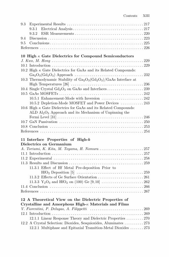
Fig. 1.4. Mobility characteristics of bi-axial strained-Si n-channel MOSFETs (a)Mobility enhancement factor as a function of Ge content in SiGe substrates, whichis in proportion to strain. Strained Si on relaxed SiGe with Ge content of 24 at %has strain of 1%. Closed circles and triangles show the experimental values in bulkand SOI MOSFETs, respectively. Solid [14] and dash [32] lines mean the results oftheoretical calculations. (b) Effective field (Eeff) dependence of electron mobility inbi-axial strained-Si nMOSFETs
of the strain is small and the strain configuration is uni-axial. It has beenshown for n-channel MOSFETs that mechanical tensile strain leads to a mo-bility increase [17, 18], also attributed to the subband energy splitting. As aconsequence, since a primary parameter for the mobility enhancement in n-channel MOSFETs is the subband energy splitting between the twofold andthe fourfold valleys, there exists no essential difference in physical mecha-nism for mobility modulation due to bi-axial and uni-axial strain, though aquantitative difference in the amount of the enhancement is seen.
The relationship between electron mobility in n-channel MOSFETs andbi-axis tensile strain parallel to MOS interfaces has been systematically inves-tigated by using strained-Si MOSFETs fabricated on relaxed SiGe substrates.Figure 1.4(a) shows the experimental results for the mobility enhancementfactor [19–31], defined by the ratio of the mobility in strained-Si MOSFETsto that in conventional (unstrained) Si MOSFETs, as a function of Ge con-tent in SiGe substrates. Here, strain in Si on relaxed SiGe with Ge contentof 24 at % amounts to strain of 1%. Results of the enhancement factor theo-retically calculated on the basis of phonon scattering are also shown [14, 32].Agreement between the experimental and theoretical results is fairly good. Itis found that maximum an enhancement factor of roughly two is obtained.
Figure 1.4(b) shows the effective field (Eeff) dependence of electron mo-bility in n-channel MOSFETs at room temperature with and without tensilestrain [29,33]. It is found that the mobility enhancement factor is almost con-stant, irrespective of Eeff . Since the mobility in moderate Eeff region is knownto be dominated by phonon scattering, the mobility enhancement in this

1 Strained-Si CMOS Technology 7
region can be explained by the mechanisms described above. In high Eeff
region, on the other hand, almost all the electrons can occupy the twofoldvalleys even without any strain, because of the increased confinement causedby strong surface electric field. Since this fact suggests that the band split-ting might have much less influence on the mobility in high Eeff region, thehigh enhancement factor experimentally observed in high Eeff region has beenattributed to the reduction in the probability of surface roughness scatter-ing [34], which dominates the mobility in high Eeff region. However, the physi-cal origin is still unclear because of the lack of direct evidence for the decreasedsurface roughness scattering.
1.3.2 Physical Origin of Mobility Enhancement inp-Channel MOSFETs
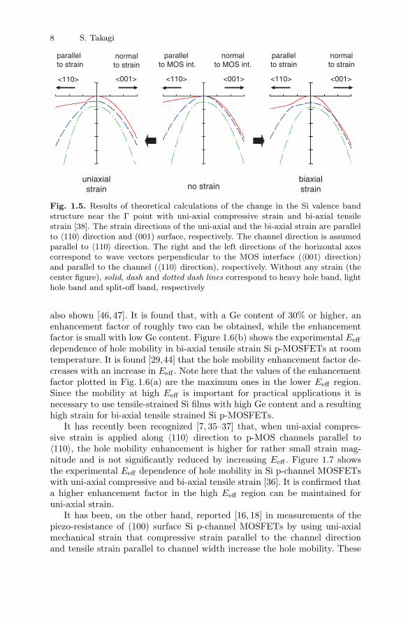
Compared with n-channel MOSFETs, the impact of strain on hole mobility inp-channel MOSFETs is complicated and the physical mechanism has not beenfully and quantitatively understood yet. Also, it has recently been recognizedin p-channel MOSFETs that the effects of uni-axial and bi-axial strain on thehole mobility are significantly different [7, 35–37], which is in contrast to n-channel MOSFETs. It has been pointed out that uni-axial compressive strainperpendicular to channel direction and bi-axial tensile strain are effective inenhancing the hole mobility in p-channel MOSFETs [38].
Figure 1.5 shows the results of theoretical calculations of the three-dimensional Si valence band structure near the Γ point with uni-axial compres-sive strain and bi-axial tensile strain [38]. Here, assuming a MOSFET channeldirection as parallel to 〈110〉, the strain directions are taken to be parallel to(001) surface for bi-axial strain and in the 〈110〉 direction for uni-axial strain.The right and the left directions of are horizontal axes in the figures in thewave vectors perpendicular to the MOS interface (along 〈001〉 direction) andparallel to the channel (along 〈110〉 direction), respectively. While, withoutany strain, the heavy hole band and the light hole band degenerate at thetop of the valence band, the application of strain leads to the band splittingand shifting the light hole band upward. As a result, the top of the valenceband is composed of the light hole band. In addition, the modulation of thecurvature of the bands due to strain provides a change in the effective massand the anisotropy in the effective mass parallel and perpendicular to theMOS interface. As a consequence, hole mobility enhancement due to strain isattributable to the following three mechanisms: (1) reduction in the effectivemass of occupied bands; (2) suppression of inter-subband scattering due to thesubband energy splitting; (3) increase in the occupancy of subbands havinghigher mobility.
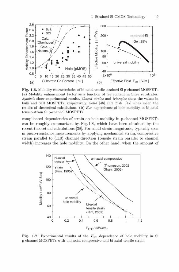
Figure 1.6(a) shows experimental results of the hole mobility enhancementfactor in bi-axial tensile-strained Si p-MOSFETs fabricated on relaxed SiGesubstrates as a function of Ge content in the SiGe substrates [20, 22, 26, 28–30,39–45]. The theoretically calculated results of the enhancement factor are
8 S. Takagi
no strainuniaxialstrain
<110><110> <110><001> <001> <001>
parallelto strain
normalto strain
biaxialstrain
parallelto strain
normalto strain
parallelto MOS int.
normalto MOS int.
Fig. 1.5. Results of theoretical calculations of the change in the Si valence bandstructure near the Γ point with uni-axial compressive strain and bi-axial tensilestrain [38]. The strain directions of the uni-axial and the bi-axial strain are parallelto 〈110〉 direction and (001) surface, respectively. The channel direction is assumedparallel to 〈110〉 direction. The right and the left directions of the horizontal axescorrespond to wave vectors perpendicular to the MOS interface (〈001〉 direction)and parallel to the channel (〈110〉 direction), respectively. Without any strain (thecenter figure), solid, dash and dotted dash lines correspond to heavy hole band, lighthole band and split-off band, respectively
also shown [46, 47]. It is found that, with a Ge content of 30% or higher, anenhancement factor of roughly two can be obtained, while the enhancementfactor is small with low Ge content. Figure 1.6(b) shows the experimental Eeff
dependence of hole mobility in bi-axial tensile strain Si p-MOSFETs at roomtemperature. It is found [29,44] that the hole mobility enhancement factor de-creases with an increase in Eeff . Note here that the values of the enhancementfactor plotted in Fig. 1.6(a) are the maximum ones in the lower Eeff region.Since the mobility at high Eeff is important for practical applications it isnecessary to use tensile-strained Si films with high Ge content and a resultinghigh strain for bi-axial tensile strained Si p-MOSFETs.
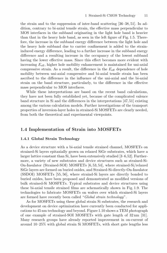
It has recently been recognized [7, 35–37] that, when uni-axial compres-sive strain is applied along 〈110〉 direction to p-MOS channels parallel to〈110〉, the hole mobility enhancement is higher for rather small strain mag-nitude and is not significantly reduced by increasing Eeff . Figure 1.7 showsthe experimental Eeff dependence of hole mobility in Si p-channel MOSFETswith uni-axial compressive and bi-axial tensile strain [36]. It is confirmed thata higher enhancement factor in the high Eeff region can be maintained foruni-axial strain.
It has been, on the other hand, reported [16, 18] in measurements of thepiezo-resistance of (100) surface Si p-channel MOSFETs by using uni-axialmechanical strain that compressive strain parallel to the channel directionand tensile strain parallel to channel width increase the hole mobility. These
1 Strained-Si CMOS Technology 9
Effective Field Eeff [ V/m ]
106
Effe
ctiv
e M
obili
ty [
cm
2 /V
s ]
100
200
300
60
40
80
2x10⁵
(b)Substrate Ge Content [ % ]0 5 10 15 20 25 30 35 40 45 50
Mob
ility
Enh
ance
men
t Fac
tor
0.8
1.0
1.2
1.4
1.6
1.8
2.0
2.2
2.4
2.6
BulkSOI
Calc.(Oberhuber)
Calc.(Nakatsuji)
Hole (pMOS)
(a)
universal mobility
strained-Si
Ge : 25%
Fig. 1.6. Mobility characteristics of bi-axial tensile strained Si p-channel MOSFETs(a) Mobility enhancement factor as a function of Ge content in SiGe substrates.Symbols show experimental results. Closed circles and triangles show the values inbulk and SOI MOSFETs, respectively. Solid [46] and dash [47] lines mean theresults of theoretical calculations. (b) Eeff dependence of hole mobility in bi-axialtensile-strain Si p-channel MOSFETs
complicated dependencies of strain on hole mobility in p-channel MOSFETscan be roughly summarized by Fig. 1.8, which have been obtained by therecent theoretical calculations [38]. For small strain magnitude, typically seenin piezo-resistance measurements by applying mechanical strain, compressivestrain parallel to 〈110〉 channel direction (tensile strain parallel to channelwidth) increases the hole mobility. On the other hand, when the amount of
uni-axial compressive
EEFF / (MV/cm)
universalhole mobility
bi-axialtensile strain(Rim, 2002)
bi-axialtensile
Mob
ility
\ cm
2 \ (
V S
ec)
0 0.240
60
80
100
120
140
0.4 0.6 0.8 1.21
strain(Rim, 1995)
(Thompson, 2002Ghani, 2003)
Fig. 1.7. Experimental results of the Eeff dependence of hole mobility in Sip-channel MOSFETs with uni-axial compressive and bi-axial tensile strain

10 S. Takagi
−0.02 −0.01 0.00 0.01 0.020
2
4
6
8
uniaxial(parallel to
channel direction)
strain
biaxial
compressive tensile
biaxial
decrease
increase
mobility
Mob
ility
enh
ance
men
t fac
tor
in p
MO
SF
ET
Fig. 1.8. Calculated results of the mobility enhancement factor for inversion-layerholes in Si p-channel MOSFETs with uni-axial compressive and bi-axial tensile strain[38]. The value of Eeff is taken to be 1MV cm−1
strain increases to some extent, both compressive and tensile bi-axial strainalso increase the hole mobility and, in particular, the mobility enhancementby tensile bi-axial strain becomes higher. It can be understood from theseresults that uni-axial compressive strain parallel to 〈110〉 channels is mosteffective for the hole mobility enhancement in p-channel MOSFETs and, ifthe amount of strain is large, bi-axial tensile strain are effective.
The difference in the Eeff dependence of the hole mobility in Si p-channelMOSFETs between uni-axial compressive and bi-axial tensile strain has beenexplained by the difference in the physical mechanism for hole mobility en-hancement for the two strain configurations. The hole mobility enhancementfor bi-axial tensile strain has been attributed mainly to the suppression ofinter-band scattering due to the band splitting between heavy hole and lighthole bands and less to the contribution of the change in the effective massdue to strain [36, 37]. In addition, the effective mass perpendicular to MOSinterfaces in the subband originating in the light hole band, which is lower inenergy, is lighter than that in the subband originating in the heavy hole band,as seen in the right figure of Fig. 1.5. As a result, the increase in the subbandenergy due to carrier confinement at MOS interfaces is higher in the light holeband than in the heavy hole band. Since this increase in the subband energydue to confinement reduces the strain-induced energy difference between thelight hole and heavy hole bands, the total amount of band splitting reduceswith an increase in Eeff and, finally, the heavy hole band becomes higher inenergy than the light hole one. This change in the band splitting has beenregarded as a main cause for the decrease in the mobility enhancement inbi-axial tensile strain p-MOSFETs with increasing Eeff . [36–38,48–50]
In contrast, the hole mobility enhancement by uni-axial compressive strainhas been attributed both to a decrease in the effective mass associated with
1 Strained-Si CMOS Technology 11
the strain and to the suppression of inter-band scattering [36–38, 51]. In ad-dition, contrary to bi-axial tensile strain, the effective mass perpendicular toMOS interfaces in the subband originating in the light hole band is heavierthan that in the heavy hole band, as seen in the left figure of Fig. 1.5. There-fore, the increase in the subband energy difference between the light hole andthe heavy hole subband due to carrier confinement is added to the strain-induced energy difference, leading to a further increase in the subband energydifference and a resulting increase in the occupancy of the lowest subbandhaving the lower effective mass. Since this effect becomes more evident withincreasing Eeff , higher hole mobility enhancement is maintained for uni-axialcompressive strain. As a result, the difference in the Eeff dependence of holemobility between uni-axial compressive and bi-axial tensile strain has beenascribed to the difference in the influence of the uni-axial and the bi-axialstrain on the band structure, particularly, to the difference in the effectivemass perpendicular to MOS interfaces.
While these interpretations are based on the recent band calculations,they have not been fully established yet, because of the complicated valenceband structure in Si and the differences in the interpretations [47,51] existingamong the various calculation models. Further investigations of the transportproperties of inversion-layer holes in strained-Si MOSFETs are clearly needed,from both the theoretical and experimental viewpoints.
1.4 Implementation of Strain into MOSFETs
1.4.1 Global Strain Technology
As a device structure with a bi-axial tensile strained channel, MOSFETs onstrained-Si layers epitaxially grown on relaxed SiGe substrates, which have alarger lattice constant than Si, have been extensively studied [3–6,52]. Further-more, a variety of new substrates and device structures such as strained-Si-On-Insulator (Strained-SOI) MOSFETs [6, 53, 54], where strained-Si/relaxedSiGe layers are formed on buried oxides, and Strained-Si-directly-On-Insulator(SSDOI) MOSFETs [55, 56], where straind-Si layers are directly bonded toburied oxides, have been proposed and demonstrated as modified versions ofbulk strained-Si MOSFETs. Typical substrates and device structures usingthese bi-axial tensile strained films are schematically shown in Fig. 1.9. Thetechnologies to fabricate MOSFETs on wafers over which strained-Si layersare formed have recently been called “Global strain technology”.
As for MOSFETs using these global strain Si substrates, the research anddevelopment on device optimization have currently been conducted for appli-cations to 45 nm technology and beyond. Figure 1.10 shows a TEM photographof one example of strained-SOI MOSFETs with gate length of 32 nm [31].Many research groups have already reported improvement in on-current ofaround 10–25% with global strain Si MOSFETs, with short gate lengths less

12 S. Takagi
(I ) Global strain technology
relaxedSi1-xGex
relaxedSi1-xGex
gateS
G
D
strained Si(tensile)
Bulk sub. SOI sub.
strained-Si
SiGe graded bufferGe: 0 % → x %
Si substrate
S
G
D
Tensile strain
gate
n+n+
n+n+
n+n+
S
G
D
buried SiO2buried SiO2
gate insulatorgate
Strained-Si/SiGe-OI Single-layerstrained-SOI
gateinsulator
gateinsulator
Si substrate Si substrate
strained Si(tensile)
Fig. 1.9. Schematic cross-sections of typical MOS structures using global bi-axialtensile strain
than sub-100 nm [31, 56–63]. The successful operation of CMOS with gatelength of 25 nm [58] and the integration of strained-Si MOSFETs with high-kgate insulators [64] and metal gates [59] have also been demonstrated.
Advantages of global strain Si MOSFETs are listed as follows: (1) large anduniform strain can be realized; (2) conventional CMOS fabrication processescan be applied with minimal modification for global strain substrates suppliedfrom wafer vendors. On the other hand, there are still many issues for practical
Fig. 1.10. TEM photograph of cross-sectional view of a strained Si-On-InsulatorMOSFET with gate length of 32 nm [31]. A trained-Si thin film, where a channelof the MOSFET is formed, and a relaxed-SiGe thin film are fabricated on a buriedoxide layer. The gate electrode is made of poly-Si and NiSi formed in source/drainregion and on the top of the poly-Si gate

1 Strained-Si CMOS Technology 13
use of this technology. For example, (1) limited performance improvement inp-channel MOSFETs with small or moderate strain (2) wafer quality includingdefects and dislocations (3) wafer cost (4) increase in junction leakage current.Also, the importance of reducing the parasitic resistance in source/drain re-gions has been pointed out for higher performance enhancement in ultra-shortgate lengths [31,63].
1.4.2 Local Strain Technology
As a technology to solve the above issues associated with global strain tech-niques, “local strain technology”, which introduces structures and materials toinduce strain into channels locally inside MOSFETs, has recently stirred keeninterest. Figure 1.11 schematically shows a variety of local strain technologies.In particular, the following two methods are quite typical.
(1) SiGe source/drain. SiGe is epitaxially grown selectively in source/drain re-gions, where are etched off toward substrates. These buried SiGe regionsinduce uni-axial compressive strain into channels, applied to p-channelMOSFETs [7, 35]. Recently, n-channel MOSFETs with tensile straininduced by selectively growing SiC in source/drain regions instead of SiGehave also been reported [65].
(2) SiN capping layer. SiN capping layers with intrinsic stress, deposited onMOSFETs as interlayer films, induce strain into MOS channels [66–68]. Inmany cases, SiN films with tensile strain have been applied to n-channelMOSFETs, while SiN films with compressive strain have recently beendeveloped and used for p-channel MOSFETs [69].
Besides these approaches local strain from isolation regions like shallowtrench isolation [70], poly-gate electrodes [71], silicide regions [72], etc. canalso be used. Judging from the fact that /SiGe source/drain and strained SiNcapping layers has been applied to logic LSI processes under 90 nm technology
S STISTI
Si sub.
D
G
SiGe or SiC
SiN inter-layer film
Fig. 1.11. Schematic illustration of a device structure using a variety of local straintechniques. STI in the figure means regions of Shallow Trench Isolation. Black andwhite arrows indicate compressive and tensile strain, respectively
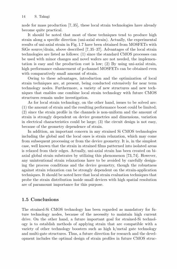
14 S. Takagi
node for mass production [7, 35], these local strain technologies have alreadybecome quite practical.
It should be noted that most of these techniques tend to produce highstrain along a specific direction (uni-axial strain). Actually, the experimentalresults of uni-axial strain in Fig. 1.7 have been obtained from MOSFETs withSiGe source/drain, above described [7, 35–37]. Advantages of the local straintechnologies are listed as follows: (1) since the standard CMOS processes canbe used with minor changes and novel wafers are not needed, the implemen-tation is easy and the production cost is low; (2) By using uni-axial strain,high performance enhancement of p-channel MOSFETs can be obtained evenwith comparatively small amount of strain.
Owing to these advantages, introduction and the optimization of localstrain techniques are, at present, being conducted extensively for near termtechnology nodes. Furthermore, a variety of new structures and new tech-niques that enables one combine local strain technology with future CMOSstructures remain under investigation.
As for local strain technology, on the other hand, issues to be solved are:(1) the amount of strain and the resulting performance boost could be limited;(2) since the strain profile in the channels is non-uniform and the amount ofstrain is strongly dependent on device geometries and dimensions, variationin electrical characteristics could be large; (3) the circuit design is not easy,because of the geometry dependence of strain.
In addition, an important concern in any strained Si CMOS technologiesincluding the global and the local ones is strain relaxation, which may comefrom subsequent processing or from the device geometry. It is, in the simplestcase, well known that the strain in strained films patterned into isolated areasis relaxed from their edges. Actually, uni-axial strain has been created on bi-axial global strain substrates by utilizing this phenomenon [73, 74]. However,any unintentional strain relaxations have to be avoided by carefully design-ing the process conditions and the device geometry, though the robustnessagainst strain relaxation can be strongly dependent on the strain-applicationtechniques. It should be noted here that local strain evaluation techniques thatprobe the strain distribution inside small devices with high spatial resolutionare of paramount importance for this purpose.
1.5 Conclusions
The strained-Si CMOS technology has been regarded as mandatory for fu-ture technology nodes, because of the necessity to maintain high currentdrive. On the other hand, a future important goal for strained-Si technol-ogy is to establish methods of applying strain that are compatible with avariety of other technology boosters such as high k/metal gate technologyand multi-gate structures. Thus, a future direction for research and the devel-opment includes the optimal design of strain profiles in future CMOS struc-

1 Strained-Si CMOS Technology 15
tures and their realization through global strain techniques, local strain tech-niques or their combination. Device/process designs for the robustness againstperformance variation and avoidance of reliability problems can are also otherimportant priorities. In order to accomplish these tasks, further comprehensiveand quantitative understanding of the effects of strain on electrical character-istics and fabrication processes as well as the metrology of strain with highresolution are strongly needed.
Acknowledgements
The author would like to thank N. Sugiyama, T. Numata, T. Mizuno,T. Tezuka, N. Hirashita, T. Maeda, T. Irisawa, K. Usuda, S. Nakaharai,Y. Moriyama, A. Tanabe, J. Koga, Y. Miyamura and E. Toyoda for theircooperation and M. Hirose, T. Kanayama, S. Kawamura, T. Masuhara andN. Fukushima for their continuous support. This work was partly supportedby the New Energy and Industrial Technology Development Organization(NEDO).
References
1. D.A. Antoniadis, Proc. VLSI Symposium, Honolulu, p. 2 (2002)2. 2004 Edition of the ITRS, http://public.itrs.net/3. F. Schaffler, Semicond. Sci. Technol. 12, p. 1515 (1997)4. C.K. Maiti, L.K. Bera and S. Chattopadhyay, Semicond. Sci. Technol. 13,
p. 1225 (1998)5. C.K. Maiti, N.B. Chakrabarti and S.K. Ray, “Strained silicon heterostructures:
materials and devices” – (IEE circuits, devices and systems series; No. 12), TheInstitute of Electrical Engineers, London, UK, 2001
6. M.L. Lee, E.A. Fitzgerald, M.T. Bulsara, M.T. Currie and A. Lochtefeld,J. Appl. Phys. 97, 011101 (2005)
7. S. Thompson, N. Anand, M. Armstrong, C. Auth, B. Arcot, M. Alavi, P. Bai,J. Bielefeld, R. Bigwood, J. Brandenburg, M. Buehler, S. Cea, V. Chikarmane,C. Choi, R. Frankovic, T. Ghani, G. Glass, W. Han, T. Hoffmann, M. Hussein,P. Jacob, A. Jain, C. Jan, S. Joshi, C. Kenyon, J. Klaus, S. Klopcic, J. Luce,Z. Ma, B. McIntyre, K. Mistry, A. Murthy, P. Nguyen, H. Pearson, T. Sandford,R. Schweinfurth, R. Shaheed, S. Sivakumar, M. Taylor, B. Tufts, C. Wallace,P. Wang, C. Weber, and M. Bohr: Int. Electron Devices Meet. Tech. Dig., SanFrancisco, p. 61 (2002)
8. K. Natori, J. Appl. Phys., 76, p. 4879 (1994)9. M.S. Lundstrom, IEEE Electron Device Lett. 18, p. 361 (1997)
10. M.S. Lundstrom, IEEE Electron Device Lett. 22, p.293 (2001)11. K. Rim, J.L. Hoyt, and J.F. Gibbons, IEEE Trans. Electron Devices, 47,
p. 1406 (2000)12. R. Ohba and T. Mizuno, IEEE Trans. Electron Devices 48, p. 338 (2001)13. A. Lochefeld and D.A. Antoniadis, IEEE Electron Device Lett., p. 591 (2001)

16 S. Takagi
14. S. Takagi, J.L. Hoyt, J.J. Welser, J.F. Gibbons, J. Appl. Phys. 80, p. 1567 (1996)
15. C.S. Smith, Phys. Rev. 94, p. 42(1954)
16. D. Colman, R.T. Bate, and J.P. Mize, J. Appl. Phys. 39, p. 1923 (1968)
17. G. Dorda, J. Appl. Phys. 42, p. 2053 (1971)
18. A. Hamada, T. Furusawa, N. Saito and E. Takeda, IEEE Trans. Electron Devices38, p. 895 (1991)
19. J.J. Welser, J.L. Hoyt, S. Takagi and J.F. Gibbons, Int. Electron Devices Meet.Tech. Dig., San Francisco, p. 373 (1994)
20. T. Mizuno, N. Sugiyama, H. Satake and S. Takagi, Proc. VLSI Symposium,Honolulu, p. 210 (2000)
21. T. Mizuno, S. Takagi, N. Sugiyama, H. Satake, A. Kurobe, and A. Toriumi,IEEE Electron Device Lett. 21, 230 (2000)
22. K. Rim, S. Koester, M. Hargrove, J. Chu, P.M. Mooney, J. Ott, T. Kanarsky,P. Ronsheim, M. Ieong, A. Grill and H.-S.P. Wong, Proc. VLSI Symposium,Kyoto, p. 59 (2001)
23. L.-J. Huang, J.O. Chu, S. Goma, C.P. D’Emic, S.I. Koester, D. F. Canaperi,P.M. Mooney, S.A. Cordes, J.L. Speidell, R.M. Anderson and H.-S.P. Wong,Proc. VLSI Symposium, Kyoto, p. 57 (2001)
24. Z.-Y. Cheng , M.T. Currie, C.W. Leitz, G. Taraschi, E.A. Fitzgerald, J.L. Hoytand D.A. Antoniadis, IEEE Electron Device Lett. 22, 321 (2001)
25. M.T. Currie, C.W. Leitz, T.A. Langdo, G. Taraschi, E.A. Fitzgerald andD.A. Antoniadis, J. Vac. Sci. Technol, B19, 2268 (2001)
26. N. Sugii, D. Hisamoto, K. Washio, N. Yokoyama and S. Kimura, Int. ElectronDevices Meet. Tech. Dig., Washington, D.C., p. 737 (2001)
27. T. Tezuka, N. Sugiyama, T. Mizuno and S. Takagi, Proc. VLSI Symposium,Honolulu, p. 96 (2002)
28. K. Rim, J. Chu, H. Chen, K.A. Jenkins, T. Kanarsky, K. Lee, A. Mocuta,H. Zhu, R. Roy, J. Newbury, J. Ott, K. Petrarca, P. Mooney, D. Lacey, S.Koester, K. Chan, D. Boyd, M. Ieong and H.-S. Wong, Proc. VLSI Symposium,Honolulu, p. 98 (2002)
29. T. Mizuno, N. Sugiyama, T. Tezuka, T. Numata, and S. Takagi, Proc. VLSISymposium, Honolulu, p. 106 (2002)
30. S. Takagi, T. Mizuno, T. Tezuka, N. Sugiyama, T. Numata, K. Usuda,S. Nakaharai, Y. Moriyama, J. Koga, A. Tanabe, N. Hirashita and T. Maeda,Int. Electron Devices Meet. Dig., p. 57 (2003)
31. T. Numata, T. Irisawa, T. Tezuka, J. Koga, N. Hirashita, K. Usuda, E. Toyoda,Y. Miyamura, A. Tanabe, N. Sugiyama and S. Takagi, Int. Electron DevicesMeet. Tech. Dig., San Francisco, p. 177 (2004)
32. M. Rashed, W.K. Shih, S. Jallepalli, T.J.T. Kwan and C.M. Maziar, Int. Elec-tron Devices Meet. Tech. Dig., Washington, D.C., p. 765 (1995)
33. T. Mizuno, N. Sugiyama, T. Tezuka, and S. Takagi, IEEE Trans. ElectronDevices 49, p. 7 (2002)
34. M.V. Fischetti, F. Gamiz, and W. Hansch., J. Appl.Phys. 92, p. 7320 (2002)
35. T. Ghani, M. Armstrong, C. Auth, M. Bost, P. Charvat, G. Glass, T. Hoff-mann, K. Johnson, C. Kenyon, J. Klaus, B. McIntyre, K. Mistry, A. Murthy,J. Sandford, M. Silberstein, S. Sivakumar, P. Smith, K. Zawadzki, S. Thompsonand M. Bohr, Int. Electron Devices Meet. Tech. Dig., Washington, D.C., p. 978(2003)

1 Strained-Si CMOS Technology 17
36. S.E. Thompson, M. Armstrong, C. Auth, S. Cea, R. Chau, G. Glass, T.Hoffman, J. Klaus, Z. Ma, B. McIntyre, A. Murthy, B. Obradovic, L. Shifren,S. Sivakumar, S. Tyagi, T. Ghani, K. Mistry, M. Bohr and Y. El-Mansy, IEEEElectron Device Lett.25, p. 191 (2004)
37. S.E. Thompson, G. Sun, K. Wu, J. Lim and T. Nishida, Int. Electron DevicesMeet. Tech. Dig., San Francisco, p. 221 (2004)
38. M. Uchida, Y. Kamakura, and K. Taniguchi, Proc. Int. Conf. Simulation ofSemiconductor Processes and Devices, p. 315 (2005)
39. K. Rim, J.J. Welser, J.L. Hoyt and J.F. Gibbons: Int. Electron Devices Meet.Tech. Dig., Washington, D.C., p. 517 (1995)
40. D.K. Nayak, K. Goto, A. Yutani, J. Murota and Y. Shiraki, IEEE Trans.Electron Devices 43, p. 1709 (1996)
41. C.K. Maiti, L.K. Bera, S.S. Dey, D.K. Nayak and N.B. Chakrabarti, SolidState Electron.41, p. 1863 (1997)
42. T. Tezuka, N. Sugiyama, S. Takagi and A. Kurobe, Abs. 25th InternationalConference on the Physics of Semiconductors, Osaka, H-270, p. 629 (2000)
43. T. Mizuno, N. Sugiyama, A. Kurobe, and S. Takagi, IEEE Trans. ElectronDevices 48, p. 1612 (2001)
44. T. Mizuno, N. Sugiyama, T. Tezuka, and S. Takagi, IEEE Trans. ElectronDevices 50, p. 988 (2003)
45. C.W. Leitz, M.T. Currie, M.L. Lee, Z.-Y. Cheng, D.A. Antoniadis andE.A. Fitzgerald, J. Appl. Phys. 92, p. 3745 (2002)
46. R. Oberhuber, G. Zandler and P. Vogl, Phys. Rev. B 58, 9941 (1998)47. H. Nakatsuji, Y. Kamakura and K. Taniguchi, Int. Electron Devices Meet.
Tech. Dig., San Francisco, p. 727 (2002)48. T. Mizuno, N. Sugiyama, T. Tezuka, T. Numata, T. Maeda and S. Takagi, Int.
Electron Devices Meet. Tech. Dig., San Francisco, p. 31 (2002)49. T. Mizuno, T. Mizuno, N. Sugiyama, T. Tezuka, T. Numata and S. Takagi,
IEEE Trans. Electron Devices 51, p. 1114 (2004)50. M.V. Fischetti, Z. Ren, P.M. Solomon, M. Yang and K. Rim, J. Appl. Phys.
94, p. 1079 (2003)51. L. Shifren, X. Wang, P. Matagne, B. Obradovic, C. Auth, S. Cea, T. Ghani,
J. He, T. Hoffman, R. Kotlyar, Z. Ma, K. Mistry, R. Nagisetty, R. Shaheed,M. Stettler, C. Weber, and M.D. Giles: Appl. Phys. Lett.85, p. 6188 (2004)
52. J.J. Welser, J.L. Hoyt and J.F. Gibbons, IEEE Electron Device Lett. 15,p. 100 (1994)
53. T. Mizuno, S. Takagi, N. Sugiyama, H. Satake, A. Kurobe, and A. Toriumi,IEEE Electron Device Lett. 21, p. 230 (2000)
54. S. Takagi, T. Mizuno, N. Sugiyama, T. Tezuka and A. Kurobe, IEICE Trans.Electron. E84-C, p. 1043 (2001)
55. T.A. Langdo, M.T. Currie, A. Lochtefeld, R. Hammond, J.A. Carlin,M. Erdtmann, G. Braithwaite, V.K. Yang, C.J. Vineis, H. Badawi, and M.T.Bulsara, Appl. Phys. Lett. 82, p. 4256 (2003)
56. K. Rim, K. Chan, L. Shi, D. Boyd, J. Ott, N. Klymko, F. Cardone, L. Tai, S.Koester, M. Cobb, D. Canaperi, B. To, E. Duch, I. Babich, R. Carruthers, P.Saunders, G. Walker, Y. Zhang, M. Steen, and M. Ieong, Int. Electron DevicesMeet. Tech. Dig., Washington, D.C., p. 49 (2003)
57. B.H. Lee, A. Mocuta, S. Bedell, H. Chen, D. Sadana, K. Rim, P. O’Neil,R. Mo, K. Chan, C. Cabral, C. Lavoie, D. Mocuta, A. Chakravarti, R.M.

18 S. Takagi
Mitchell, J. Mezzapelle, F. Jamin, M. Sendelbach, H. Kermel, M. Gribelyuk,A. Domenicucci, K.A. Jenkins, S. Narasimha, S.H. Ku, M. Ieong, I.Y. Yang,E. Leobandung, P. Agnello, W. Haensch, and J. Welser, Int. Electron DevicesMeet. Tech. Dig., San Francisco, p. 946 (2002)
58. J.-S. Goo, Q. Xiang, Y. Takamura, H. Wang, J. Pan, F. Arasnia, E. N. Paton,P. Besser, M.V. Sidorov, E. Adem, A. Lochtefeld, G. Braithwaite, M.T. Currie,R. Hammond, M.T. Bulsara and M.-R. Lin: IEEE Electron Device Lett. 24,p.351 (2003)
59. Q. Xiang, J.-S. Goo, J. Pan, B. Yu, S. Ahmed, J. Zhang, and M. -R. Lin, Proc.VLSI Symposium, Kyoto, p. 101 (2003)
60. J.R. Hwang, J.H. Ho, S.M. Ting, T.P. Chen, Y.S. Hsieh, C.C. Huang, Y.Y.Chiang, H.K. Lee, A. Liu, T.M. Shen, G. Braithwaite, M.T. Currie, N. Gerrish,R. Hammond, A. Lochtefeld, F. Singaporewala, M.T. Bulsara, Q. Xiang, M.R.Lin, W.T. Shiau, Y.T. Loh, J.K. Chen, S.C. Chien, S.W. Sun and Frank Wen,Proc. VLSI Symposium, Kyoto, p. 103 (2003)
61. H.C.-H. Wang, Y.-P. Wang, S.-J. Chen, C.-H. Ge, S.M. Ting, J.-Y. Kung,R.-L. Hwang, H.-K. Chiu, L.C. Sheu, P.-Y. Tsai, L.-G. Yao, S.-C. Chen, H.-J.Tao, Y.-C. Yeo, W.-C. Lee, and C. Hu, Int. Electron Devices Meet. Tech. Dig.,Washington, D.C., p.61 (2003)
62. T. Sanuki, A. Oishi, Y. Morimasa, S. Aota, T. Kinoshita, R. Hasumi, Y.Takegawa, K. Isobe, H. Yoshimura, M. Iwai, K. Sunouchi and T. Noguchi, Int.Electron Devices Meet. Tech. Dig., Washington, D.C., p. 65 (2003)
63. H. Kawasaki, K. Ohuchi, A. Oishi, O. Fujii, H. Tsujii, T. Ishida, K. Kasai, Y.Okayama, K. Kojima, K. Adachi, N. Aoki, T. Kanemura, D. Hagishima, M.Fujiwara, S. Inaba, K. Ishimaru, N. Nagashima and H. Ishiuchi, Int. ElectronDevices Meet. Tech. Dig., San Francisco, p. 169 (2004)
64. K. Rim, E.P. Gusev, C.D. Emic, T. Kanarsky, H. Chen, J. Chu, J. Ott, K.Chan, D. Boyd, V. Mazzeo, B.H. Lee, A. Mocuta, J. Welser, S.L. Cohen, M.Ieong and H.-S. Wong, Proc. VLSI Symposium, Honolulu, p. 12 (2002)
65. K.W. Ang, K.J. Chui, V. Bliznetsov, A. Du, N. Balasubramanian, M.F. Li, G.Samudra and Y.-C. Yeo, Int. Electron Devices Meet. Tech. Dig., San Francisco,p. 1069 (2004)
66. F. Ootsuka, S. Wakahara, K. Ichinose, A. Honzawa, S. Wada, H. Sato, T. Ando,H. Ohta, K. Watanabe, and T. Onai, Int. Electron Devices Meet. Tech. Dig.,San Francisco, p. 575 (2000)
67. S. Ito, H. Namba, K. Yamaguchi, T. Hirata, K. Ando, S. Koyama, S. Kuroki,N. Ikezawa, T. Suzuki, T. Saitoh, and T. Horiuchi, Int. Electron Devices Meet.Tech. Dig., San Francisco, p. 247 (2000)
68. A. Shimizu, K. Hachimine, N. Ohki, H. Ohta, M. Koguchi, Y. Nonaka, H. Sato,and F. Ootsuka, Int. Electron Devices Meet. Tech. Dig., Washington, D.C.,p. 433 (2001)
69. H.S. Yang, R. Malik, S. Narasimha, Y. Li, R. Divakaruni, P. Agnello, S. Allen, A.Antreasyan, J.C. Arnold, K. Bandy, M. Belyansky, A. Bonnoit, G. Bronner, V.Chan, X. Chen, Z. Chen, D. Chidambarrao, A. Chou, W. Clark, S.W. Crowder,B. Engel, H. Harifuchi, S.F. Huang, R. Jagannathan, F.F. Jamin, Y. Kohyama,H. Kuroda, C.W. Lai, H.K. Lee, W. Lee, E.H. Lim, W. Lai, A. Mallikarjunan,K. Matsumoto, A. McKnight, J. Nayak, H.Y. Ng, S. Panda, R. Rengarajan,M. Steigerwalt, S. Subbanna, K. Subramanian, J. Sudijono, G. Sudo, S. Sun, B.Tessier, Y. Toyoshima, P. Tran, R. Wise, R. Wong, I.Y. Yang, C.H. Wann, L. T.

1 Strained-Si CMOS Technology 19
Su, M. Horstmann, T. Feudel, A. Wei, K. Frohberg, G. Burbach, M. Gerhardt,M. Lenski, R. Stephan, K. Wieczorek, M. Schaller, H. Salz, J. Hohage, H. Ru-elke, J. Klais, P. Huebler, S. Luning, R. van Bentum, G. Grasshoff, C. Schwan,E. Ehrichs, S. Goad, J. Buller, S. Krishnan, D. Greenlaw, M. Raab, and N.Kepler, Int. Electron Devices Meet. Tech. Dig., San Francisco, p. 1075 (2004)
70. S. Tiwari, P.M. Mooney, M.V. Fischetti and J.J. Welser, Int. Electron DevicesMeet. Tech. Dig., Washington, D.C., p. 939 (1997)
71. K. Ota, K. Sugihara, H. Sayama, T. Uchida, H. Oda, T. Eimori, H. Morimotoand Y. Inoue, Int. Electron Devices Meet. Tech. Dig., San Francisco, p. 27 (2002)
72. Z. Krivokapih, V. Moroz, W. Maszara, M.-R. Lin, Int. Electron Devices Meet.Tech. Dig., Washington, D.C., p. 445 (2003)
73. H. Yin, K.D. Hobart, R.L. Peterson, S.R. Shieh, T.S. Duffy, and J.C. Sturm,Appl. Phys. Lett. 87, 061922 (2005)
74. T. Irisawa, T. Numata, T. Tezuka, K. Usuda, N. Hirashita, N. Sugiyama, E.Toyoda and S. Takagi, Proc. VLSI Symposium, Kyoto, p. 178 (2005)

2
High Current Drivability MOSFETFabricated on Si(110) Surface
A. Teramoto and T. Ohmi
Summary. This chapter demonstrates CMOS device characteristics on the Si(110)surface by using a surface flattening process and radical oxidation. By forming aMOS device on the Si(110) surface, high-speed and low flicker noise p-MOSFETscan be realized. Furthermore, the current drivability of p-MOS and n-MOS whichare balanced in the CMOS (balanced CMOS) on Si(110) surface can also be real-ized. These devices are very useful for application to analog/digital mixed signalcircuits.
2.1 Introduction
Miniaturization of metal oxide silicon field effect transistor (MOSFET) hasbeen able to increase the integration and performance of LSI devices. However,miniaturization of the critical dimension of integrated circuits is accompaniedby a decrease in thickness of gate insulator films for MOS transistors. Leakagecurrents are mainly composed of leakage current through the gate insulatorfilms and the drain leakage current. Suppression of the leakage current in ULSIdevices is one of the crucial requirements for an improvement of ULSI devices.Improvement of current drivability of MOSFETs without shrinkage of the de-vice scale is also very important for increasing LSI performance. Efforts toincrease device performance using strained silicon [1–4], Fin-FETs [5–7], etc.have recently been reported. In addition, Si(110) surface channel devices havealso been investigated [8–14]. It has been reported that the hole mobility inthe channel on Si(110) is largest compared with other low-index surfaces [15].Figure 2.1 shows the dependence of the effective mobility of electrons andholes in the channel on Si surface orientation and channel direction [15].Altering the crystalline orientation of the Si surface channel has the advan-tage that it is possible to increase in the current drivability without changingthe material and the device structure. However, present-day gate formationtechnology cannot form high quality insulator films on the Si(110) surface. Wereported that very high quality gate insulators can be formed on every silicon

22 A. Teramoto and T. Ohmi
(001) (013)(023) (133) (111) (211)(411) (100)(233)(011) (322) (311)(811)
500
400
300
200
100
0
6.0
5.0
4.0
3.0
2.0
0
1.0
250
200
150
100
50
0
8.0
6.0
4.0
2.0
00−45 45
⊥<100>
⊥<100>
⊥<011>
ELECTRONS
⊥<011>
⊥<011>
⊥<011>
HOLES
// 011
90
<100> zone <011> zone
//<100>//<011>
//<011>
//<011>
//<011>
µFE(Obs.);300K, VG-VT = 25Vme/mij(Calc.)
µ FE
[cm
2 /V
.sec
]µ F
E[c
m2 /
V.s
ec]
me/m
ijm
e/m
ij//<011>
µFE(Obs.);300K, VG-VT = −25Vme/mij(Calc. by MAEDA)
Fig. 2.1. Dependence of the effective mobility of electrons and holes in the channelon the Si surface orientation and channel direction [15]
surface by microwave-exited high-density plasma oxidation/nitridation, andvery low 1/f noise is realizing by using this oxidation/nitridation technol-ogy [8, 16].
In this chapter, we demonstrate that low noise balanced CMOS that isvery useful for analog/digital mixed signal circuits can be fabricated on a verysmooth Si(110) surface by using a newly developed five-step room temperatureclean and the microwave-excited high-density plasma oxidation process.
2.2 Experimental
Dual gate-MOSFETs on Cz–Si(100) and Cz–Si(110) surfaces are emp-loyed in these experiment. Five nanometer gate oxides are formed by the

2 High Current Drivability MOSFET Fabricated on Si(110) Surface 23
Fig. 2.2. Five-steps room temperature wet cleaning [20]
microwave-excited high-density plasma oxidation (radical oxidation) at 400Cafter modified RCA cleaning [17–19] and five-steps room temperature wetcleaning [20] (shown in Fig. 2.2). As+ and BF2
+(4 × 1015 cm−2) ions are im-planted to the gate poly-Si (300 nm) and source/drain regions after gate for-mation for n-MOSFET and p-MOSFET, respectively. After the formationof an aluminium interconnect, hydrogen sintering is performed at 400C inN2/H2 = 9/1.
Surface micro-roughness and dissolution of Si atoms into water also evalu-ated. The silicon surfaces are treated by five-steps room temperature cleaningand the RCA cleaning following diluted HF dipping/UPW rinse. As a result,native oxide was not formed on both of the silicon surfaces studied. SurfaceMicro-roughness of the silicon surfaces is evaluated by vacuum scanning tun-nelling microscopy (STM) and the atomic force microscopy (AFM) after theRCA and five-steps room temperature cleaning. The surface micro-roughnessand Si dissolution into water measured by the inductive coupled plasma Augerelectron spectroscope (ICP-AES) are also evaluated after immersion in watercontaining various dissolved oxygen concentrations of 0 (N2 ambient), 8 ppm(O2/N2 = 1/4), and 32 ppm (O2 ambient).

24 A. Teramoto and T. Ohmi
(100) (110) (111) (100) (110) (111)
Al Gate MOSTOX=10 nm
Radical oxidation Dry oxidation
1012
1011
1010
109
Inte
rfac
e tr
ap d
ensi
ty a
t mid
gap
(eV
−1cm
−2)
Fig. 2.3. SiO2/Si interface trap density formed by radical oxidation at 400 C andthermal oxidation at 900C [14]
2.3 Results and Discussions
2.3.1 MOSFET Characteristics on the Si(110) Surface
Static Characteristics of MOSFET Fabricated on Si(110)
Figure 2.3 shows the interface trap density at the Si/SiO2 interface formed bythe radical oxidation (400C) and by conventional dry oxidation (900C) onSi(100), Si(110) and Si(111) oriented surfaces [14]. It is well-known that highquality SiO2 films and Si/SiO2 interface having a low interface trap densitycan be realized by the thermal oxidation only on Si(100) surface as shown inFig. 2.3. However, as shown in Fig. 2.3, radical oxidation using the microwaveexcited high density plasma can form high quality SiO2 films and Si/SiO2
interface having a low interface trap density on every silicon surface orienta-tion. This means that every silicon surface can be applied to LSI formation
L = 100umW = 300umTox = 5nmVD = 50mV
(110) S - factor 63.43mV/dec
10−3
10−4
10−5
10−6
10−7
10−8
VG [V] VG [V]0 −1 −2 −3
(100) S - factor 62.48mV/dec
I D/C
ox[A
/F]
(a)
L = 100um
W = 300um
Tox = 5nmVD = 50mV
(110) S - factor 68.64mV/dec
(100) S - factor 64.91mV/dec
10−3
10−4
10−5
10−6
10−7
10−8
0 −1 −2 −3
I D/C
ox[A
/F]
(b)
Fig. 2.4. ID − Vg characteristics of p-channel MOSFETs. (a) The gate oxide wasformed by radical oxidation. (b) The gate oxide was formed by the dry oxidation

2 High Current Drivability MOSFET Fabricated on Si(110) Surface 25
0
1
6
5
4
3
2
0
1
6
5
4
3
2
Drain Voltage (VD) [V] Drain Voltage (VD) [V]0 −1 −2 −3 0 −1 −2 −3
Dra
in C
urre
nt (
I D)
[×10
−4A
]
Dra
in C
urre
nt (
I D)
[ ×10
−4A
]
Tox=5nm
W=100umL =100um
Tox=5nm
W=100umL =100um
VG-VTH = −0.5VVG-VTH = −1.0V
VG-VTH = −1.5VVG-VTH = −2.0V
VG-VTH = −2.5V
VG-VTH = −2.5V
VG-VTH = −2.0V
VG-VTH = −1.5V
VG-VTH = −1.0V
VG-VTH = −0.5V
Fig. 2.5. ID − VD characteristics of p-MOSFETs on Si(100) and Si(110) surfaces.The current drivability of p-MOSFET on Si(110) is three times larger than that onSi(100)
by using radical oxidation. Figure 2.4 shows the drain current (ID)-gate volt-age (VG) characteristics (drain voltage (VD) = 50mV) of p-MOSFETs havinggate oxides formed by (a) radical oxidation and (b) dry oxidation. In the caseof dry oxidation, a difference in threshold voltage appears on Si(100) andSi(110), as a result Si/SiO2 interface traps and fixed charge in the gate ox-ide. No threshold voltage shift is observed between the MOSFETs on Si(110)and Si(100) having gate oxide formed by the radical oxidation. This indicatesthat radical oxidation can be used for gate oxide formation on Si(110) sur-faces. Figure 2.5 shows the ID − VD characteristics of p-MOSFETs on (a)Si(100) and (b) Si(110). The current drivability of p-MOSFET on Si(110) isthree times larger than that on Si(100). Figure 2.6 shows the effective channelmobility (µeff) as a function of effective electric field (Eeff) in the p-channelMOSFET. Eeff is defined by (QB + Qi/η)/εsi, where η of n- and p-MOSFET
101 101
102
103 102
0.1 1.0 0.1 1.0
(100)
(100)
(110)
(110)
Effective Electric Field (MV/cm) Effective Electric Field (MV/cm)
Effe
ctiv
e ho
le M
obili
ty(c
m2 /
V•s
ec)
(110) T.Mizuno et al.,[4]
(110) T.Mizuno et al.,[4]
Effe
ctiv
e E
lect
ron
Mob
ility
(cm
2 /V
•sec
)
Fig. 2.6. Effective channel mobility (µeff) as a function of an effective electric field(Eeff). µeff of p-MOSFET on Si(110) is much larger than that on Si(100) and is alsolarger than that reported µeff on Si(110) [4]

26 A. Teramoto and T. Ohmi
<-110>
60nm×60nm
<-110>
1um×1um
Ra = 0.170 [nm]Rms = 0.213 [nm]
(a) AFM (b) STM
Fig. 2.7. (a) AFM image and (b) STM image of (110) silicon surface after UPWfinal rinse at RCA cleaning. The lines like trough to the 〈−110〉 direction areobserved
are taken to be 2 and 3, respectively [4] and εsi is dielectric constant of asilicon. µeff of the p-MOSFET on Si(110) is much larger than that on Si(100)and is also larger than that reported µeff on Si(110) [4,21,22]. This may resultfrom the formation of higher-quality oxides on the Si/SiO2 interface usingradical oxidation. However, µeff of the n-MOSFET on Si(110) is the same asthat reported previously for Si(110) [4] and less than that for Si(100).
Figure 2.7 shows (a) AFM and (b) STM images of the Si(110) surface afterUPW final rinse at RCA cleaning and diluted HF treatment. Lines parallel tothe 〈−110〉 direction are observed. This suggests that surface micro-roughnesson Si(110) surface is caused by RCA cleaning resulting in degradation of thechannel mobility for n-MOSFETs. Figure 2.8 shows the average surface micro-roughness (Ra) change for the Si(110) surface after wet oxidation at 1,000C orradical oxidation at 400C. Both high temperature wet oxidation and radicaloxidation are isotropic oxidation processes. Therefore, both oxidations havea surface flattening effect. Figure 2.9 shows the (a) AFM and (b) STM im-ages of the Si(110) surface after H2-UPW+ megasonic rinse at the end of thefive-step cleaning [20] (shown in Fig. 2.2) for either wet oxidation or radical
0.00
0.05
0.10
0.15
0.20
0.25
beforeoxidation
beforeoxidation
afterpeeling
afterpeeling
(a) at field oxidation (b) at gate oxidation
Ra
[nm
]
radical ox. (5nm)wet ox. (370nm)
Fig. 2.8. Average surface micro-roughness (Ra) change for Si(110) surface by thewet oxidation at 1,000C and the radical oxidation at 400C

2 High Current Drivability MOSFET Fabricated on Si(110) Surface 27
60nm×60nm
<-110>
<-110>
1um×1um
Ra = 0.157 [nm]Rms = 0.197 [nm]
(a) AFM (b) STM
Fig. 2.9. (a) AFM and (b) STM images of Si(110) surface after H2-UPW + mega-sonic rinse at five-steps cleaning
oxidation. Wide terraces are seen in the STM images. This indicates thatthe micro-roughness of the Si(110) surface can be suppressed by a combi-nation of a flattening process (e.g. wet and radical oxidations) and a clean-ing technology that does not generate surface micro-roughness (e.g. the five-steps room temperature wet cleaning). Figure 2.10 shows µeff -Eeff character-istics of conventional and Si/SiO2 flattened n-MOSFETs. The µeff value canbe improved by Si/SiO2 flattening. Figure 2.11 shows the channel directiondependency of the normalized ID on Si(110). Normalized ID is defined asID/(conventional ID〈110〉). ID of flattened n-MOSFETs is larger than thatof conventional devices for every channel direction. On the other hand, thedrain currents have a strong dependence on the channel direction, and chan-nel directions giving a maximum current for n-channel MOSFETs differs fromthat of p-channel MOSFETs by 90. Figure 2.12 shows the noise power as afunction of frequency (f). The noise power is proportional to 1/f . The 1/fnoise of p-MOSFET on Si(110) is 1 order of magnitude smaller, althoughcurrent drivability is the as same as for n-MOSFETs on Si(100). This is
102
103
0.1 1Eeff [MV/cm]
µ eff
[cm
2 V−1
sec−
1 ]
conventional
Flattened
Fig. 2.10. µeff -Eeff characteristics of conventional and Si/SiO2 flattened n-MOSFETs. The µeff value can be improved by Si/SiO2 flattening

28 A. Teramoto and T. Ohmi
9045
1.4
1.3
1.2
1.1
1.0
0.90 180135
<110> <110><100>
Nor
mal
ized
Dra
in C
urre
nt
Channel direction
conventional
Flattened
VG-VTH=2V
VD=3V
L/W=100/100um
Fig. 2.11. Channel direction dependency of normalized ID on Si(110). NormalizedID is defined as ID/(conventional ID〈110〉)
consistent with the observation that the Si/SiO2 interface is very smooth afterprocessing [16].
Dependence of the Noise Characteristics of MOSFETs onMicro-Roughness [23]
Typical results of electronic noise measurements performed on p-MOSFETsfabricated on Si(100) are shown in Fig. 2.13. Several measurements were madefor all combinations of cleaning and oxidation procedures. The combinationof radical oxidation [8, 13] and the five-step room temperature clean [20] isvery effective in reducing the 1/f noise in MOSFETs compared with con-ventional thermal oxidation and RCA clean [17–19]. This suggests that thesurface roughness of Si(100) before oxidation and after the conventional RCAcleaning is larger than that for the alkali-free five-step room-temperature cleandescribed above. The improvement factor of surface micro-roughness after thefive-step clean is around 10% compared with a conventional RCA clean.
The same procedures described above has been carried out on Si(110)p-MOSFETs. Looking at the results of 1/f noise measurements shown inFig. 2.15 and at the AFM images presented on Fig. 2.16, and then comparingthem to those obtained for the conventional orientation, we can achieve alarger reduction of low frequency noise and a better improvement of the micro-roughness by once more simply changing the pre-gate formation cleaning tothe five-steps room temperature clean. The cleaning process appears to havean impact that is much more pronounced on Si(110) than on Si(100). Thedegradation of the surface resulting from RCA cleaning shown in Fig. 2.16a,which is far worse compared to that shown in Fig. 2.14a, can be explainedby the fact that the alkali solution etch rate of Si(110) is faster than thatof Si(100) [24]. This significant change in the noise level has its origin in thecleaning process and the resulting surface quality of the Si/SiO2 interface andin particular the change in the surface micro-roughness.
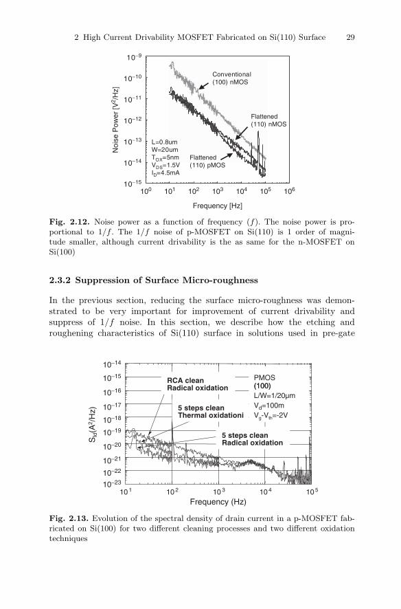
2 High Current Drivability MOSFET Fabricated on Si(110) Surface 29
Frequency [Hz]
100 101 102 103 104 105 106
Noi
se P
ower
[V2 /
Hz]
10−9
10−10
10−11
10−12
10−13
10−14
10−15
Conventional(100) nMOS
Flattened(110) nMOS
Flattened(110) pMOS
L=0.8umW=20umTOX=5nmVDS=1.5VID=4.5mA
Fig. 2.12. Noise power as a function of frequency (f). The noise power is pro-portional to 1/f . The 1/f noise of p-MOSFET on Si(110) is 1 order of magni-tude smaller, although current drivability is the as same for the n-MOSFET onSi(100)
2.3.2 Suppression of Surface Micro-roughness
In the previous section, reducing the surface micro-roughness was demon-strated to be very important for improvement of current drivability andsuppress of 1/f noise. In this section, we describe how the etching androughening characteristics of Si(110) surface in solutions used in pre-gate
5 steps cleanRadical oxidation
5 steps cleanThermal oxidationi
RCA cleanRadical oxidation
SId(A
2 /H
z)
10−14
10−15
10−16
10−17
10−18
10−19
10−20
10−21
10−22
10−23
10 1 10 2 10 3 10 4 10 5
Frequency (Hz)
(100)
Vd=100mVg-Vth=-2V
PMOS(100)L/W=1/20µm
Fig. 2.13. Evolution of the spectral density of drain current in a p-MOSFET fab-ricated on Si(100) for two different cleaning processes and two different oxidationtechniques

30 A. Teramoto and T. Ohmi
Fig. 2.14. Micro-roughness Ra and peak-valley maximum amplitude P–V after theRCA clean (a) and the five-step clean (b) for Si(100)
oxide water cleaning compare with the characteristics of the Si(100) sur-face [25]. The Si(110) surface is etched and roughened easily by solutionscontaining OH− ions compared to the observed etch rate of Si(100).
Hydrogen termination of the Si surface is often used to passivate it againstcontamination, native oxidation, and so on. The silicon surface terminated byhydrogen is chemically stable [26]. In this section, hydrogen termination ofSi(110) surface is also described. The hydrogen terminated Si(110) surface isvery weakly passivated against native oxidation compared with the hydrogenterminated Si(100) surface, and as a result, precise control of the process at-mosphere is essentially required for high performance devices to be fabricatedon the Si(110) surface.
10−23
SId
(A2 /
Hz)
10−14
10−15
10−16
10−17
10−18
10−19
10−20
10−21
10−22
101 102 103 104 105
Frequency (Hz)
(110)PMOS(110)L/W=1/20µmVd=−100mVVg-Vth=−2V
5 steps cleanTermal oxidation
RCA cleanRadical oxidation
5 steps cleanRadical oxidation
Fig. 2.15. Evolution of the spectral density of drain current in p-MOSFET fab-ricated on Si(110) for two different cleaning processes and two different oxidationtechniques
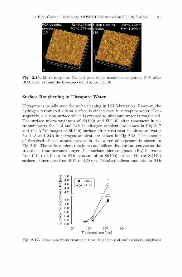
2 High Current Drivability MOSFET Fabricated on Si(110) Surface 31
Fig. 2.16. Micro-roughness Ra and peak-valley maximum amplitude P–V afterRCA clean (a) and the five-step clean (b) for Si(110)
Surface Roughening in Ultrapure Water
Ultrapure is usually used for wafer cleaning in LSI fabrication. However, thehydrogen terminated silicon surface is etched even in ultrapure water. Con-sequently, a silicon surface which is exposed to ultrapure water is roughened.The surface micro-roughness of Si(100) and Si(110) after treatment in ul-trapure water for 1, 3 and 24 h in nitrogen ambient are shown in Fig. 2.17and the AFM images of Si(110) surface after treatment in ultrapure waterfor 1, 3 and 24 h in nitrogen ambient are shown in Fig. 2.18. The amountof dissolved silicon atoms present in the water of exposure is shown inFig. 2.19. The surface micro-roughness and silicon dissolution increase as thetreatment time becomes longer. The surface microroughness (Ra) increasesfrom 0.12 to 1.16 nm for 24 h exposure of on Si(100) surface. On the Si(110)surface, it increases from 0.12 to 4.58 nm. Dissolved silicon amounts for 24 h
0.00.20.40.60.81.01.2
101 102 103 104
Treatment time [min]
Sur
face
mic
roro
ughn
ess;
Ra
[nm
]
4.64.4
4.85.0
4.2
(100)(110)
Fig. 2.17. Ultra-pure water treatment time dependence of surface micro-roughness

32 A. Teramoto and T. Ohmi
Ra; 4.83nmP-V; 31.7nm
Ra; 0.283nmP-V; 5.08nm
Ra; 0.104nmP-V; 1.85nm
hour 3 hours 24 hours
Fig. 2.18. AFM images of Si(110) surface after ultra-pure water treatment of 1,3, 24 h
from Si(100) and Si(110) correspond to 91 and 200 atomic layers removed, asdetermined. The results from the dissolved silicon data are consistent with thesurface micro-roughness data. Therefore, the surface micro-roughness degra-dation is attributed to silicon dissolving into ultrapure water during longtermexposure. More silicon atoms are dissolved into ultra-pure water from theSi(110) orientation wafer compared with the Si(100) orientation. The silicondissolution reaction is assumed to result from oxidation of the surface byhydroxide ions (OH−). OH− ions in ultrapure water can etch silicon atoms asalkali solutions [25]. Silicon atoms are dissolved as HSiO3
− and SiO32− ions
in aqueous solution. Although the treatment time examined in these experi-ments is longer than industrial rinsing processes, which are typically only afew minutes, dissolving of silicon atoms during the rinsing process for evenshort times can increase the surface micro-roughness. However, suppression ofsurface micro-roughness is one of the most important issues for improvement
101 102 103 104
Am
ount
of d
isso
lved
sili
con
[X 1
016at
oms
/cm
2]
100
101
102
10−1
10−2
Surface Si of (110)
Surface Si of (100)
Treatment time [min]
(100)
(110)
Fig. 2.19. Ultrapure water treatment time dependence of amount of dissolvedsilicon.

2 High Current Drivability MOSFET Fabricated on Si(110) Surface 33
0.0
1.0
2.0
3.0
4.0
5.0
6.0
0 10 20 30 40 50 60
IPA concentration [wt%]
Sur
face
mic
roro
ughn
ess
; Ra
[nm
]
P (100)
P (110)
Time: 24 hoursTemperature: RTAtmosphere: nitrogen
(100)
(110)
Fig. 2.20. Dependence on IPA concentration in UPW of the surface micro-roughness
of the channel mobility in the MOSFET. Therefore rinsing solution which donot etch and roughen the Si surface are required.
Suppression of Surface Micro-roughness Using IPA/UPWSolutions
The surface micro-roughness after 24 h treatment in Isopropyl alcohol (IPA)containing solutions (< 60wt%) are shown in Fig. 2.20. The typical AFMimages are shown in Fig. 2.21 and the resulting amounts of dissolved siliconatoms in each solution are shown in Fig. 2.22. The surface roughening is sup-pressed with an increase of the IPA concentration for both of Si(100) andSi(110) surfaces. For the Si(100) surface, the suppression saturates at 5 wt%IPA concentration while it saturates at 30 wt% IPA concentration for Si(110).The amount of dissolved silicon atoms is also decreased with an increase ofthe IPA concentration. These results indicate that 5 and 30 wt% IPA additionare sufficient to suppress the surface roughening for (100) and (110) orienta-tion silicon, respectively. At those compositions, the dissolved silicon atomsdecreased to an amount corresponding to a few atomic layers for both (100)and (110) orientation. These values are very small compared with the situa-tion for ultrapure water without IPA addition. In 5 and 30 wt% IPA added toultrapure water, the molecular ratios (water:IPA) of water and IPA are about63:1 and 7.8:1. Although water molecules are still the major component ineach solution, the reactions to dissolve silicon atoms are prevented at thesilicon surface by the hydrophobic property of IPA. As a result, the surfaceroughening is suppressed with IPA added to ultrapure water.
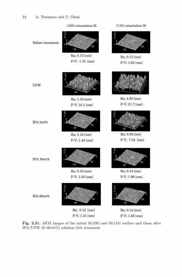
34 A. Teramoto and T. Ohmi
Ra;Ra; 0.13 [nm]0.13 [nm]
P-V; 1.85 [nm]P-V; 1.85 [nm]
Ra; 0.14 [nm]Ra; 0.14 [nm]
P-V; 1.96 [nm]P-V; 1.96 [nm]
Ra; 0.14 [nm]Ra; 0.14 [nm]
P-V; 1.56 [nm]P-V; 1.56 [nm]
Ra; 0.92 [nm]Ra; 0.92 [nm]
P-V; 7.24 [nm]P-V; 7.24 [nm]
Ra; 4.83 [nm]Ra; 4.83 [nm]
P-V; 31.7 [nm]P-V; 31.7 [nm]
Ra; 0.13 [nm]Ra; 0.13 [nm]
P-V; 1.70 [nm]P-V; 1.70 [nm]
Ra; 1.16 [nm]Ra; 1.16 [nm]
P-V; 10.1 [nm]P-V; 10.1 [nm]
Ra; 0.10 [nm]Ra; 0.10 [nm]
P-V; 1.53 [nm]P-V; 1.53 [nm]
Ra; 0.12 [nm]Ra; 0.12 [nm]
P-V; 1.43 [nm]P-V; 1.43 [nm]
Ra; 0.12 [nm]Ra; 0.12 [nm]
P-V; 1.31 [nm]P-V; 1.31 [nm]
(100) orientation Si(100) orientation Si (110) orientation Si(110) orientation Si
IPA 5wt%IPA 5wt%
Before treatmentBefore treatment
IPA 30wt%IPA 30wt%
IPA 60wt%IPA 60wt%
UPW
Fig. 2.21. AFM images of the initial Si(100) and Si(110) surface and those afterIPA/UPW (0–60wt%) solution 24 h treatment

2 High Current Drivability MOSFET Fabricated on Si(110) Surface 35
0
2
4
6
8
10
12
14
16
18
20
0 10 20 30 40 50 60
IPA concentration [wt%]
amou
nt o
f dis
solv
ed s
ilico
n[x
1016
ato
ms/
cm2 ]
P(100 )P(110 )
Time: 24 hours
Temperature: RT
Atmosphere: nitrogen
(100)(110)
Fig. 2.22. Amount of dissolved silicon into IPA/UPW solution as a function of IPAconcentration
Hydrogen Termination of Silicon Surfaces
On the Si(100) surface, hydrogen termination is chemically stable [26].Figure 2.23 shows the characteristic thermal desorption spectroscopy (TDS)results for hydrogen from a Si(100) surface treated by dilute HF and UPWrinsing. Two peaks at 380 and 520C are observed in this graph [28]. A sil-icon atom in the Si(100) surface is terminated by two hydrogen atoms [29](shown in Fig. 2.24). A dangling bond from a silicon atom, which is generatedby desorption of one of two hydrogen atoms bonds gives rise to the featureat 380C. The remaining hydrogen is desorbed from the Si(100) surface at
0.0
0.5
1.0
1.5
2.0
2.5
0 200 400 600 800wafer temperature [wafer temperature [°C]
Rel
ativ
e Io
n In
tens
ity [%
]
Fig. 2.23. Thermal desorption characteristics of the hydrogens from Si(100) surfacetreated by dilute HF and UPW rinsing

36 A. Teramoto and T. Ohmi
380C 505C
:H atom : Si atom
Fig. 2.24. Schematic molecular model of the hydrogen-terminated Si(100) surface
520C [28]. Hydrogen is desorbed from the Si(110) surface only at 530C(shown in Fig. 2.25).
Figure 2.26 shows the characteristics of the TDS characteristics of (A)Si(100) and (B) Si(110) surfaces just after dilute HF treatment and UPWrinsing and after exposure to air for 2 and 12 h after dilute HF treatmentand UPW rinsing. Only the peak from hydrogen desorbed at 530C decreasesfor the Si(100) surface after exposure to the air for 2 h. Both desorption fea-tures for hydrogen at 530 and 380C decrease after exposing the passivatedSi(100) surface to the air for 12 h. Figure 2.27 shows the quantity of Si–Obonds as evaluated by an attenuated total reflectance Fourier transform in-frared (ATR/FT-IR) spectrometry. While the extent of hydrogen terminationdecreased, the Si–O bonds on the Si(100) surface increased. This means thatthe Si(100) surface is oxidized as desorption of the surface hydrogen termina-tion occurs. Figure 2.28 shows a schematic structure of (A) the Si(100) surfaceterminated by two hydrogens a silicon atom, (B) the Si(100) surface partiallyterminated by hydrogen after desorption at 380C, and (C) the Si(110) sur-face terminated by hydrogen. In order to oxidize the surface (A), the oxygenatom must replace the terminating hydrogen atoms on the surface, or oxygenmust enter into the back bond of the surface silicon atoms. Since the Si–H
0.0
0.5
1.0
1.5
2.0
2.5
0 200 400 600 800
wafer temperature [wafer temperature [°C]
Rel
ativ
e Io
n In
tens
ity [%
]
Fig. 2.25. TDS characteristics of hydrogen from the Si(110) surface treated bydilute HF and UPW rinsing

2 High Current Drivability MOSFET Fabricated on Si(110) Surface 37
200 400 600 8000wafer temperature [wafer temperature [°C]
0.0
0.5
1.0
1.5
2.0
2.5
Rel
ativ
e Io
n In
tens
ity [%
]
0.0
0.5
1.0
1.5
2.0
2.5
Rel
ativ
e Io
n In
tens
ity [%
]
(A) Si(100)(A) Si(100)
200 400 600 8000wafer temperature [wafer temperature [°C]
(B) Si(110)(B) Si(110)
No exposure2 hours12 hours
No exposure2 hours12 hours
Fig. 2.26. TDS characteristics of (A) Si(100) and (B) Si(110) surfaces just afterdilute HF treatment and UPW rinsing and after exposure to air for 2 and 12 h afterdilute HF treatment and UPW rinsing
bond of the Si(100) surface is stable and the back bond of silicon cannot beexposed easily to the O2 or H2O molecules, when the hydrogen terminationof the Si(100) surface is carried out completely, it is very hard to oxidize in.In the case of (B) and (C) surfaces, since a combination of two adjacent sil-icon atoms appears in the surface, these silicon atoms are easily oxidized byoxygen in the atmosphere. The electrons in the Si–H covalent bonds of thepartially-oxidized Si(100) surface oxidized silicon can be attracted toward theoxygen atoms because of their large electronegativity (Oxygen: 3.0). Bondsformed by surface silicon atoms to species other than oxygen (hydrogen atomsand silicon atoms in the case of Si(100) surface, and Si(110) surface, respec-tively) become weaker, and oxidization of the silicon surface is acceleratedfurther. In the case of the Si(110) surface, the oxidization of the surface isoccurs much more readily than for the initially hydrogen-terminated Si(100).Thus, native oxide growth on HF-treated Si(110) cannot be suppressed in theair. It is concluded that wet processes and transfer atmosphere before the
1300 1200 1100 1000−0.01
0.00
0.01
0.02
0.03
0.04
0.05
abso
rban
ce
−0.01
0.00
0.01
0.02
0.03
0.04
0.05
abso
rban
ce
wave number [cm−1]1300 1200 1100 1000
wave number [cm−1]
(A) Si(100)(A) Si(100) (B) Si(110)(B) Si(110)
0h
2h
12h
0h
2h
12h
Fig. 2.27. Quantity of Si–O bond evaluated by an ATR/FT-IR spectrometry
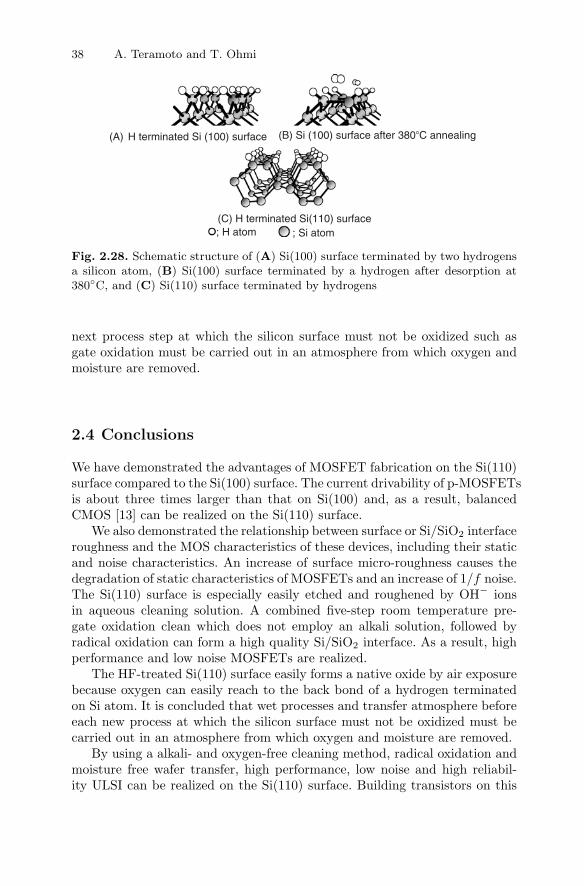
38 A. Teramoto and T. Ohmi
(A) H terminated Si (100) surface
(C) H terminated Si(110) surface; H atom ; Si atom
(B) Si (100) surface after 380C annealing
Fig. 2.28. Schematic structure of (A) Si(100) surface terminated by two hydrogensa silicon atom, (B) Si(100) surface terminated by a hydrogen after desorption at380C, and (C) Si(110) surface terminated by hydrogens
next process step at which the silicon surface must not be oxidized such asgate oxidation must be carried out in an atmosphere from which oxygen andmoisture are removed.
2.4 Conclusions
We have demonstrated the advantages of MOSFET fabrication on the Si(110)surface compared to the Si(100) surface. The current drivability of p-MOSFETsis about three times larger than that on Si(100) and, as a result, balancedCMOS [13] can be realized on the Si(110) surface.
We also demonstrated the relationship between surface or Si/SiO2 interfaceroughness and the MOS characteristics of these devices, including their staticand noise characteristics. An increase of surface micro-roughness causes thedegradation of static characteristics of MOSFETs and an increase of 1/f noise.The Si(110) surface is especially easily etched and roughened by OH− ionsin aqueous cleaning solution. A combined five-step room temperature pre-gate oxidation clean which does not employ an alkali solution, followed byradical oxidation can form a high quality Si/SiO2 interface. As a result, highperformance and low noise MOSFETs are realized.
The HF-treated Si(110) surface easily forms a native oxide by air exposurebecause oxygen can easily reach to the back bond of a hydrogen terminatedon Si atom. It is concluded that wet processes and transfer atmosphere beforeeach new process at which the silicon surface must not be oxidized must becarried out in an atmosphere from which oxygen and moisture are removed.
By using a alkali- and oxygen-free cleaning method, radical oxidation andmoisture free wafer transfer, high performance, low noise and high reliabil-ity ULSI can be realized on the Si(110) surface. Building transistors on this

2 High Current Drivability MOSFET Fabricated on Si(110) Surface 39
alternative Si surface plane provides very effective improvements in ULSI with-out shrinking of device dimensions.
Acknowledgements
The authors gratefully acknowledge Professors K. Endo, M. Morita and Dr.K. Arima of Osaka University for STM measurements and discussions. Theauthors also acknowledge the Ministry of Economy, Trade and Industry andthe New Energy and Industrial Technology Development Organization fortheir financial support.
References
1. J.J. Welser, J.L. Hoyt and J.F. Gibbons, “Electron Mobility Enhancementin Strained-Si N-Type Metal-Oxide-Semiconductor Field-Effect Transistors,”IEEE Electron Devices Lett., EDL-15, 1994, pp. 100–102
2. K. Rim, J.J. Welser, J.L. Hoyt and J.F. Gibbons, “Enhanced Hole Mobili-ties in Surface-channel Strained-Si p-MOSFETs,” in IEDM Tech. Dig., 1995,pp. 517–520, December 1995
3. S. Takagi, J.L. Hoyt, J.J. Welser and J.F. Gibbons, “Comparative study ofphonon-limited mobility of two-dimensional electrons in strained and unstrainedSi metal-oxide-semiconductor field-effect transistors,” J. Appl. Phys., Vol. 80,1996, pp. 1567–1577
4. T. Mizuno, N. Sugiyama, A. Kurobe and S. Takagi, “Advanced SOI P-MOSFETs with Strained-Si Channel on SiGe-on-Insulator Substrate Fabri-cated by SIMOX Technology,” IEEE Trans. Electron Devices, ED-48, 2001,pp. 1612–1618
5. D. Hisamoto, W. Lee, J. Kedzierski, E. Anderson, H. Takeuchi, K. Asano, T.King, J. Bokor, and C. Hu, “A Folded-channel MOSFET for Deep-sub-tenthMicron Era,” in IEDM Tech. Dig., 1998, pp. 1032–1034, December 1998
6. F. Yang, H. Chen, F. Chen, Y. Chan, K. Yang, C. Chen, H. Tao, Y. Choi,M. Liang, and C. Hu, “35 nm CMOS FinFETs,” Symp. on VLSI Tech., 2002,pp. 104–105, June 2002
7. B. Yu, L. Chang, S. Ahmed, H. Wang, S. Bell, C-Y. Yang, C. Tabery, C. Ho, Q.Xiang, T-J. King, J. Bokor, C. Hu, M-R. Lin, and D. Kyser, “Fin FET scalingto 10 nm Gate Length,” in IEDM Tech. Dig., 2002, pp. 251–254, December 2002
8. S. Sugawa, I. Ohshima, H. Ishino, Y. Saito, M. Hirayama, and T. Ohmi, “Ad-vantage of Silicon Nitride Gate Insulator Transistor by using Microwave-ExitedHigh-Density Plasma for applying 100 nm Technology Node,” in IEDM Tech.Dig., 2001, pp. 817–820, December 2001
9. T. Mizuno, N. Sugiyama, T. Tezuka, Y. Moriyama, S. Nakaharai, and S. Takagi,“[110]-surface strained-SOI CMOS devices with higher carrier mobility,” in VLSITech. Dig., 2003, pp. 97–98, June 2003
10. H. Nakamura, T. Ezaki, T. Iwamoto, M. Tago, N. Ikarashi, M. Hane, and T.Yamamoto. “Channel direction impact of (110) surface Si substrate on per-formance improvement in sub-100nm MOSFETs,” in Ext. Abst. SSDM, 2003,pp. 718–719

40 A. Teramoto and T. Ohmi
11. H. Momose, T. Ohguro, K. Kojima, S. Nakamura, and Y. Toyoshima, “1.5-nm Gate Oxide CMOS on (110) Surface-Oriented Si Substrate,” IEEE Trans.Electron Devices, vol. 50, No. 4, 2003, pp. 1001–1008
12. H. Momose, T. Ohguro, K. Kojima, S. Nakamura, and Y. Toyoshima, “110GHzcutoff frequency of ultra-thin gate oxide p-MOSFETs on [110] surface orientedSi substrate,” in VLSI Tech. Dig., 2002, pp. 156–157, June 2002
13. A. Teramoto, T. Hamada, H. Akahori, K. Nii, T. Suwa, K. Kotani, M. Hirayama,S. Sugawa and T. Ohmi, “Low noise balanced-CMOS on Si(110) surface foranalog/digital mixed signal circuits,” IEDM Tech. Dig., pp. 801–804, December2003
14. A. Teramoto, T. Hamada, M. Yamamoto, P. Gaubert, H. Akahori, K. Nii, M.Hirayama, K. Arima, K. Endo, S. Sugawa, and T. Ohmi, “High PerformanceCMOS on Si(110) surface,” to be submitted to IEEE Trans. Electron Devices
15. T. Sato, Y. Takeishi, H. Hara, and Y. Okamoto, “Mobility Anisotropy of Elec-trons in Inversion Layers on Oxidized Silicon Surfaces,” Phys. Rev. B, Vol. 4,No. 6, pp. 1950–1960, September 1971
16. K. Tanaka, K. Watanabe, H. Ishino, S. Sugawa, A. Teramoto, M. Hirayama, andT. Ohmi, “A Technology for Reducing Flicker Noise for ULSI Applications,”Jpn. J. Appl. Phys. Vol. 42, No. 4B, pp. 2106–2109, April 2003
17. W. Kern and D.A. Puotinen, “Cleaning solutions based on hydrogen perox-ide for use in silicon semiconductor technology,” RCA Review, Vol. 31, No. 2,pp. 187–206, June 1970
18. Tadahiro Ohmi, Koji Kotani, Akinobu Teramoto, and Masayuki Miyashita, “De-pendence of Electron Channel Mobility on Si SiO2 Interface Microroughness”,IEEE Electron Device Letters, Vol. 12, No. 12, pp. 652–654, December 1991
19. T. Ohmi, M. Miyashita, M. Itano, T. Imaoka, and I. Kawanabe, “Dependenceof thin oxide films quality on surface microroughness,” IEEE Trans. ElectronDevices, Vol. 137, No. 4, pp. 537–545, March 1992
20. Tadahiro Ohmi, “Total Room Temperature Wet Cleaning for Si Substrate Sur-face,” J. Electrochem. Soc., Vol. 143, No. 9, pp. 2957–2964, September 1996
21. S. Takagi, A. Toriumi, M. Iwase, and H. Tango, “On the Universality of InversionLayer Mobility in Si MOSFET’s: Part II-Effects of Surface Orientation,” ” IEEETrans. Electron Devices, vol.41, No.12, pp. 2363–2368, December 1994
22. S. Takagi, A. Toriumi, M. Iwase, and H. Tango, “On the Universality of In-version Layer Mobility in Si MOSFET’s: Part I-Effects of Substrate ImpurityConcentration,” IEEE Trans. Electron Devices, vol. 41, No. 12, pp. 2357–2362,December 1994
23. P. Gaubert, A. Teramoto, K. Kotani, and T. Ohmi, “Reduction of 1/f noisein Si(110) and (100) surface MOSFET using a new cleaning technology,” Pro-ceedings, 20th Annual Meeting of Japanese Association for Science Art andTechnology of Fluctuations, pp. 28–30, September 2005
24. H. Akahori, K. Nii, A. Teramoto, S. Sugawa, and T. Ohmi, “Atomic Order Flat-tening of Hydrogen-Terminated Si(110) Substrate For Next Generation ULSIDevices,” Extend Abstracts of the 2003 Int. Conf. SSDM, pp. 458–459, Septem-ber 2003
25. M. Yamamoto, K. Nii, H. Morinaga, A. Teramoto, and T. Ohmi, “Suppressionof Surface Micro-Roughness of Silicon Wafer by Addition of Alcohol into UltraPure Water for Rinsing Process,” To be published in ECS 208th meeting Pro-ceedings Volume Cleaning Technology in Semiconductor Device ManufacturingIX

2 High Current Drivability MOSFET Fabricated on Si(110) Surface 41
26. T. Ohmi, “Surface Chemical Electronics at the Semiconductor Surface,” Appl.Surf. Sci., Vol. 121/122, pp. 44–62, November 1997
27. K. Satoa, M. Shikidaa, T. Yamashiroa, M. Tsunekawaa, S. Itob, “Roughen-ing of single-crystal silicon surface etched by KOH water solution Sensors andActuators,” 73, pp. 122–130 (1999)
28. N. Yabumoto, K. Minegishi, K. Saito, M. Morita and T. Ohmi, “An Analysisfor Cleaned Silicon Surface with Thermal Desorption Spectroscopy,” J. Ruzylloand R.E. Novak, eds., Semiconductor Cleaning Technology/1989, PU90-5,pp. 265–272, The Electrochemical Society, Pennington, NJ, 1990
29. Y.J. Chabal, G.S. Higashi, and K. Raghavachari, “Infrared spectroscopy ofSi(111) and Si(100) surfaces after HF treatment: Hydrogen termination andsurface morphology,” J. Vac. Sci. Technol. A7(3), pp. 2104–2109, May/Jun 1989

3
Advanced High-MobilitySemiconductor-on-Insulator Materials
B. Ghyselen, I. Cayrefourcq, M. Kennard, F. Letertre,T. Akatsu, G. Celler, and C. Mazure
Summary. Silicon-on-Insulator (SOI) is today the substrate of choice for severalapplications. In order to boost further circuit performance, new solutions are beingexplored. In particular, increasing the charge carrier mobility has been identifiedas a requirement for the next technology nodes. One possible option is to increasetransistor channel mobility through local strain engineering via external stressors, anapproach that can be used on bulk silicon as well as standard SOI substrates. Othersolutions are based on substrate engineering. The attractiveness of these solutionsis largely due to their compatibility with standard CMOS integration processesand architectures and presents the advantage of being independent of transistorgeometry. The two approaches can be combined to maximize transistor mobilityand on-current. Among the different substrate level approaches, we will focus onthree main families: (1) the effect of crystal orientation, (2) strained Si and/or SiGelayers On Insulator, and (3) monocrystalline Ge-On-Insulator substrates.
3.1 Introduction
Silicon-on-insulator (SOI) is today the substrate of choice for several appli-cations, for example high performance and low power ICs. In order to boostfurther circuit performance, new solutions are being explored at the CMOSprocess level. In particular, increasing the charge carrier mobility has beenidentified as a requirement to meet the performance needs of the 65 nm tech-nology nodes and beyond.
One possible option is to increase transistor channel mobility throughlocal strain engineering via stressors like nitride layers or epitaxial SiGesource/drain pockets. This so-called “local strain” or “process-induced strain”approach can be used on bulk silicon as well as standard SOI substrates.Other solutions are to induce a MOSFET carrier mobility increase via sub-strate engineering, which presents the advantage of being independent of tran-sistor geometry. The attractiveness of wafer level based solutions is largelydue to their compatibility with standard CMOS integration processes and
44 B. Ghyselen et al.
architectures. The two approaches can be combined to maximize transistormobility and on-current.
Among the different substrate level approaches to increased mobilities inSOI architectures, we will focus on three main families:
(1) The effect of crystal orientation on carrier mobility and specific combina-tions of crystalline orientations of semiconductor layers on Insulator,
(2) Strained Si and/or SiGe layers On Insulator, and(3) Monocrystalline Ge-On-Insulator substrates.
In each case, we will give an overview of the development status at thesubstrate level and examples of device performance enhancement.
3.2 Crystalline Orientation Effects
3.2.1 Silicon Crystalline Orientations for Bulk Substrates
The principle of this approach is to take advantage of the fact that the chargecarrier mobility is dependent on the current flow direction in the crystal.Historically, (100) oriented bulk substrates with flat or notch location definingthe 〈110〉 axis have been the universal standard in the IC industry: see forinstance SEMI standards for 200 and 300 mm polished monocrystalline siliconwafers [SEMI M1.9-0699 and SEMI M1.15-0704, respectively]. The reasonsbehind this choice were to maximize electron mobility, with (100) surfaceshaving the additional advantage of forming good quality gate oxides.
Figure 3.1 [1] shows a comparison of the effect of different crystallineorientations on both the electron mobility (Fig. 3.1a) and the hole mobil-ity (Fig. 3.1b). It can be seen that while the standard choice for (100)/〈110〉wafers is indeed good for electrons, it is not the case for holes. To increase holemobility, other surface orientations shall be preferred, such as (110) wafers.The gain may be substantial, a factor 2 to 3 depending on the hole currentdirection flow in the plane. If we stay with (100) wafers, a hole mobility gainin the 10–20% range can be obtained by aligning the PMOS channel alongthe 〈100〉 directions, which is easily implemented by rotating the substrate(twist) by 45 [2–4]. At the wafering level it corresponds to a change of thenotch or flat position, which has no or minor impact on ingot pulling and onthe wafer manufacturing. This solution has the advantage that it does notaffect the electron mobility, as opposed to other crystalline orientations forwhich higher hole mobilities are obtained but at the expense of an electronmobility degradation. This advantage has been reported for unstrained sili-con [2, 3]. But it has also been demonstrated to be valid for locally strainedsilicon [4] where the strain induced gain on NMOS was not lost by rotatingby 45 the channel flow of the electrons.
For bulk substrates however, changing the crystalline orientations of theactive layer means also changing the properties of the handle substrate.

3 Advanced High-Mobility Semiconductor-on-Insulator Materials 45
(b)(a)
100
200
300 150
100
50
0.0
(100)/<110>(100)/<110>
(110)/<100>(110)/<110>
(110)/<100>
(111)/<112>
(100)/<110>
0.0 5.0×10125.0×10121.0×1013
1.0×10131.5×1013 1.5×10¹³
Ninv (cm−2) Ninv (cm−2)
(111)/<112>
Ele
ctro
n M
obili
ty (
cm2 V
−1S
−1)
Ele
ctro
n M
obili
ty (
cm2 V
−1S
−1)
Fig. 3.1. Carrier mobility in the inversion layer with various substrate orientations(gate oxides grown simultaneously in N2O at 800C in conventional furnace), forelectrons (a) and holes (b). From [1]
This may have important consequences. For instance resistance to mechanicalshocks during handling, die separation and to thermal shocks may be changed,which needs to be taken into account. Rotating the wafers by 45 means alsothat the cut plane is at 45 angle to the preferred (110) cleavage plane. Theselimitations are also characteristic of SOI substrates realised from one singlebulk substrate (see [6] for a review): SIMOX or other processes based onepitaxy (ZMR, FIPOS, etc.).
3.2.2 Silicon Crystalline Orientations for SOI Substrates
Historically, SOI wafers have duplicated bulk silicon substrates as far as pos-sible. This is the main reason why most of the SOI substrates used today(that could be called in this respect “standard SOI wafers”) are composed ofa (100)/〈110〉 SOI thin film lying on identically oriented (100)/〈110〉 handlesubstrate, as shown in Fig. 3.2a. But SOI wafers do not have to be limited toa duplication of bulk silicon wafers, they can also extend their capabilities. Inparticular for SOI substrates made using techniques based on wafer bondingand layer transfer (such as BSOI, Smart Cut or ELTRAN, see [6]) two dif-ferent substrates are used as starting material for the fabrication of one SOIwafer. This has the advantage that the choice of crystalline orientation for theactive layer and for the handle substrate can be decoupled and optimized toget the best of both orientations. The choice for the active layer can be guidedby optimizing the electrical properties–and especially the charge carrier mo-bility–while for the handle substrate the historical (100)/〈110〉 substrate canbe kept for mechanical robustness reasons.
The first simple example of non-standard SOI substrates is based on rotat-ing the donor substrate (active layer) by 45 compared to the handle substrate,as shown in Fig. 3.2b. This is something that can be achieved quite easily. Itcan be done by rotating one wafer compared to the other at the bonding stage.Or it can be done even more easily by using a donor wafer that has been ro-tated during notch/flat formation steps. Either way, the standard orientation

46 B. Ghyselen et al.
SOI : Traditional configuration
(100)
<110>
(100)
<110>
Handle wafer SOI filmTransistors aligned with <110>
SOI film rotated 45º
(100
)
<110>
(100)
<110>
Handle wafer SOI filmTransistors aligned
with <100>
<100>
(110) Device layer
(110)
<110>
(100)
<110>
Handle wafer SOI filmNMOS & PMOS in (110) plane
Fig. 3.2. Examples of combinations of crystalline orientations in SOI substratebased on layer transfer techniques: (a) traditional configuration (b) 45 (100) SOIfilm rotation. PMOS mobility is increased, NMOS mobility is unchanged [2–4] (c)(110) device layer. PMOS is enhanced, NMOS mobility is reduced [1]
is kept for the handle substrates, maintaining the way the SOI wafers willcleave during die separation, while optimizing carrier mobility. The deviationof such a process from standard SOI wafers processes is small and can beimplemented easily.
Another example is based on the use of (110) Si wafer for the donor sub-strate while keeping unchanged the base substrate (regular (100) wafer). Therethe gain is more significant in terms of hole mobilities (a factor that can be aslarge as 2–3), but at the expense of a degradation on the electron side. Thedeviation in wafer fabrication as compared to standard SOI wafers is slightlylarger since (110) layers have to be processed. It is well known [7] that somephysical and chemical properties (cleaning, oxidation, implantation) are some-what dependent on crystal orientation. From an SOI substrate manufacturing

3 Advanced High-Mobility Semiconductor-on-Insulator Materials 47
Fig. 3.3. “Hybrid Orientation Technology” (HOT), PFET on (110) surface andnFET on (100) surface. From [1]
point of view, most of it however may look more like engineering work thanprofound developments. From a device manufacturing point of view, (110)interface states densities and gate insulator properties need to be evaluated.Another practical difference is that (110) bulk material of appropriate qualityis needed. Crystal ingot growth as well as wafering steps are involved. For thespecific case of Smart Cut, layer splitting within (110) silicon and realisationof (110) SOI layers lying on (100) substrates has already been investigatedand demonstrated with some optimizations [8].
When both NMOS and PMOS transistors are built on the same crystallineplane, certain performance compromises are necessary. A concept that hasbeen emerging especially in high performance ICs, is the possibility of com-bining different layers and addressing separately the improvement of NMOSand PMOS transistors. Figure 3.3 describes schematically the hybrid orienta-tion technology (HOT) approach [1]. Thanks to the flexibility of wafer bondingand layer transfer techniques, it combines the conventional (100) orientation(notch oriented towards 〈110〉 direction) to address NMOS and a (110) orien-tation for PMOS. In one case the (100) oriented layer is the SOI film (NMOSSOI) while the bulk PMOS is built on a (110) layer grow epitaxially fromthe handle substrate [1]. The inverse crystal orientation combination resultsin (110) SOI PMOS and (100) bulk NMOS.
3.2.3 Perspectives for Crystalline Orientations in SOI Substrates
Deviating from the traditional “Full (100)/〈110〉 oriented silicon substrates”several examples of crystalline orientation evolutions and combination withinSOI substrates have been described.
Overall, the advantages of these advanced engineered substrates address-ing improved mobilities is that they are still “standard silicon” and “standardSOI” structures. In that respect, such solutions do not represent major com-plications to the existing processes and can be implemented easily from anSOI substrate manufacturing point of view.
It should be kept in mind that only a few simple examples have been de-scribed here. The door is open to other crystalline orientations that would

48 B. Ghyselen et al.
appear more appropriate, and also to more complex substrate structures,with more than one SOI layer to address more than one type of transistor.The optimum crystalline orientation may also depend on whether (and whichkind of) strain is applied to the silicon to boost carrier mobilities [5]. As aconclusion, revisiting crystalline orientations should be kept in mind whendesigning advanced generations of devices and substrates. This is also valid forthe next sections where other clues to higher carrier mobilities – like strainedSi- and other materials – like Ge- are addressed.
3.3 Strained Si on Insulator Wafers
3.3.1 Introduction to Strained Si on Insulator Wafers
It has been known for a long time that straining semiconductors has an im-pact on their carrier mobilities. It is true for silicon, for SiGe and Ge, andalso for most of III–V materials. Strain can be tensile or compressive, biax-ial or uniaxial, parallel or transverse to the current flow. Its effect on carriermobilities can be positive or negative, and is not equivalent for electrons andholes. The impact of strain on carrier mobilities, although far from being per-fectly known and understood, has been documented quite extensively in theliterature, especially for the case of silicon: see for instance this book andother references [10–13]. Briefly, conduction or valence band degeneracy split-ting, preferential thermal population of electron states with light transporteffective mass, reduced interband/intervalley hole/electron-phonon scatteringhave been used to explain mobility changes [this book + [10–12].
There are several ways to achieve controlled strain levels in silicon. Beforegoing into the specifics of SOI architectures, we will first briefly describe twobasic concepts for introducing strain in CMOS transistor channels: the so-called “local strain” and “global strain” approaches. Later we will focus onglobal strain, considering different manufacturing routes for substrates thatcombine strained Si layers and SOI architectures. Two types of substrates willbe considered depending on whether the final strained SOI wafer containsany SiGe layer. These SOI-based structures are known as SGOI, when anintermediate layer of SiGe is present between strained Si and the buried oxide(BOX), and sSOI when strained Si is placed directly on the BOX. While manytechniques look compatible with the realization of SGOI substrates, we willshow the unique capability of layer transfer techniques to make Ge-free sSOI.In particular, it will be shown that thin strained films can be transferred tonew substrates and that the wafer bonding interface alone can stabilize thebuilt-in strain in adjacent layers.
3.3.2 “Local Strain”
The approach referred to as “local strain” or “process-induced strain”, is basedupon the uniaxial strain that is introduced during the CMOS manufacturing

3 Advanced High-Mobility Semiconductor-on-Insulator Materials 49
Fig. 3.4. TEM cross-section of NMOS (a) device capped with stressed silicon nitrideand PMOS (b) device showing the SiGe epitaxial source and drain stressors [14]
steps [14–22], such as epitaxial SiGe source/drain pocket formation, ni-tride spacer deposition, gate encapsulation, shallow trench isolation (STI).Figure 3.4 [14], shows a TEM cross-section of NMOS with tensile strain in-ducing gate liner and a compressive strain inducing SiGe source/drain stressor.
Uniaxial stressors are generated and introduced during CMOS manufac-turing. It has proven very successful and leading edge IC makers have im-plemented it in 90 nm technology manufacturing. The drawback of uniaxialstressors is that these are device geometry dependent by their nature. Thelateral dimensions of the transistors affect the efficiency and the strength ofthe induced strain. Strain engineering needs to be taken into account at thetransistor and IC design level, limiting the technology flexibility to a cell li-brary approach. For each new technology node a redesign of the stressors isneeded in order to achieve a mobility increase. Defectivity is another criticalparameter. The presence of strong strain gradients associated with the localstrain approach may generate crystalline defects that would result in excessivepn junction leakage or generate device failure. Local strain techniques havebeen industrially implemented in bulk as well as in SOI technologies.
3.3.3 “Global Strain”
Global strain is a further step in strain engineering to further boost devicemobility and current drive. It helps overcome the limitations of uniaxial tech-niques, and its combination with local strain techniques is proposed to max-imize performance for the future technology nodes. It has the advantage ofbeing independent of a specific MOSFET geometry, and it applies to large andsub-µm devices. Global strain is not only an alternative but can be combinedwith process induced strain to enable the optimization of both NMOS andPMOS transistors.
The fabrication of bulk strained silicon is critical. A strained Si layer isgrown by hetero-epitaxy on a relaxed Si1−xGex layer, the final strain beingan increasing function of the Ge content. Since bulk SiGe substrates withGe concentrations above 10% do not exist, virtual substrates with relaxed

50 B. Ghyselen et al.
Relaxed SiGe
Si Substrate
Graded buffer
220F1QS_01g_220_4200x
1 µm
C
Fig. 3.5. TEM cross-section of a virtual SiGe substrate realized with graded buffer.Only the very surface is eventually useful for the overgrowth of strained Si layer
SiGe are first formed by hetero-epitaxy on bulk Si with the help of differentepitaxial techniques. These include forming graded buffers or low temperaturebuffers that allow for the SiGe lattice to relax to its equilibrium value. Thisis followed by a low crystal defect epitaxial step in order to fabricate a goodquality surface [23–27]. A similar technique is also used in the compoundmaterials field [28]. Figure 3.5 shows as an example a TEM cross-section of avirtual SiGe substrate realized with a graded buffer.
Increasing the Ge content of the SiGe substrate increases the strain withinthe overlying silicon layer. Figure 3.6 [29] shows experimentally that for elec-trons a mobility improvement beyond 60% can be achieved for Ge content>18%. For holes, no real gain appears until Ge content reaches 30–40%. Forsuch values the gain in hole mobility becomes very significant: more than 100%improvement is possible.
Technical challenges increase with the Ge content of the films. Thisis especially true for the epitaxial layers (increasing dislocations densities,
Mob
ility
Enh
ance
men
t Fac
tor
2.2Calculation (based on 2DEG)
EXP.(Rim, Huang, 2001)
bulk
SO
EXP.(Welser, 1994)
3.4Comparison with µ
Comparison with control
Rim, 1995
Rim, 1995Nayak, 1996Maiti, 1997
Calculation(Oberhuber)
300 K
Mizuno, 2000 (Strained SOI)Huang, 2001 (Strained SOI)
universalTezuka, 2000
3.23.02.82.62.42.22.01.81.61.41.21.00.8
Substrate Ge Content [ % ] Substrate Ge Content [ % ]
300 K
EXP.(Rim, 1998)
EXP. for Strained SOI(Mizuno, 2000)
2.0
1.8
1.6
1.4
1.2
1.0
0.80 5 10 15 20 25 30 35 40 40 450 5 10 15 20 25 30 35 50
Fig. 3.6. Calculated and measured carrier mobility enhancement factors as publish-ed by Tagaki et al. [29]. The left figure is for electrons and the right one for holes

3 Advanced High-Mobility Semiconductor-on-Insulator Materials 51
pile-ups, cross-hatch), but also for other process steps such as cleaning orthermal treatments. This is one reason why 20% Ge was chosen for the firstgeneration of strained films: a compromise between the electron mobility im-provement and wafer fabrication technology. A second generation of strainedsubstrates, with 35–40% Ge content will address an improved hole mobility.
3.3.4 Two Main Approaches to “Global Strain On Insulator”:SGOI Vs. sSOI
SGOI: Strained Si on Insulator via IntermediateRelaxed SiGe Layer On Insulator
Many forms of strained SOI contain at least one thin buried relaxed SiGelayer in addition to the strained Si layer. The role of this layer is to enablethe formation of the strain within the Si layer. Usually an SiGeOI substrateis formed first, and then it is used as a template for the final Si epitaxialdeposition step. For the latter to be strained, it is important that the SiGelayer On Insulator is relaxed. The relaxation rate, combined with the initial Gecontent, determine how strained the silicon layer will be, and ultimately howmuch the transistor performance will be enhanced. This approach is called“SGOI”.
In SGOI, the strain value and the crystalline quality of the overgrownstrained Si layer depend on the quality of the underlying SiGeOI layers. Thegrowth of the final strained silicon layer is relatively routine. The main tech-nical challenge is in making appropriate relaxed SiGeOI substrates. In thefollowing sections we will describe different routes that have been demon-strated to realize these structures. Since SGOI involves two semiconductorlayers on insulator, the total thickness of the active device region is typicallyabout 30–70 nm, which is suitable for partially depleted (PD) transistors.
sSOI: Strained Si on Insulator Without anyIntermediate SiGe Layer
Schematically, the sSOI substrate is a simple evolution of the standard SOIsubstrate, with a strained Si layer replacing the conventional relaxed Si film.The sSOI substrate does not contain any additional SiGe layer. Compared toSGOI, however, this apparently simple sSOI substrate can be realized only bylayer transfer techniques. The main advantages of sSOI are its full compati-bility with SOI technology, no Ge contamination risk of the strained Si andelimination of the SiGe/sSi interface which is a source for misfit dislocationnucleation.
Ge is seen by some end-users as an additional and potentially parasitic ele-ment to control. Using sSOI substrates becomes therefore a critical advantagefor IC makers. The absence of Ge in sSOI eliminates a potential problem ofGe out-diffusion within the transistor active area and increases the flexibility

52 B. Ghyselen et al.
of the device fabrication process flow. sSOI structures are typically very thinand this makes them very suitable for fully depleted technology. It will beshown later that sSOI films can also be made thick enough for PD devices orfor multiple gate transistors such as FinFETs.
The two approaches (sSOI and SGOI) can also be compared in terms oftheir sensitivity to misfit dislocations. In strained epitaxial stacks, relaxationtends to occur thanks to the easy formation of misfit dislocations. These havea very detrimental effect on device behavior when located close to the activearea. In the case of SGOI, the danger is that such misfit dislocations mayeasily appear at the SiGe/strained Si interface.
3.3.5 Different Routes Towards SGOI
Several substrate strategies have been investigated for the formation of relaxedSiGeOI substrates. They include the following:
(a) SIMOX technology. Similarly to standard SOI manufacturing by SIMOX,a high dose of oxygen is implanted within a substrate in order to separatethe active layer from the rest of the bulk substrate. The main differenceis that an additional epitaxial SiGe layer is formed before the oxygen im-plant [30], as illustrated in Fig. 3.7. Usually in SIMOX, a high temperature(>1,300C) annealing is performed to promote oxygen diffusion and pre-cipitation into the buried oxide, and also to annihilate crystalline defectscreated in the top silicon layer. For SGOI formation this final high temper-ature anneal is still necessary and it limits severely the initial Ge contentof the SiGe layer, since its melting point drops with the increase in Geconcentration. It should also be noted that the overall process enables arelaxation of the SiGe layer. Currently it seems there is not much activityto develop further the SIMOX-based process, which may be explained bythe emergence of other more promising approaches.
(b) “Ge condensation effect” [31]. This approach, as illustrated in Fig. 3.8,starts with a “standard” SOI substrate on which an SiGe layer is
Si
Strained-SiGe Relaxed-
SiGe
Relaxed-SiGe
O+
(1) Initial (2) SIMOX
RP
(3) ITOX
Burled-SiO2
Fig. 3.7. SIMOX process adapted to the realization of SiGeOI substrates (from [30])

3 Advanced High-Mobility Semiconductor-on-Insulator Materials 53
Fig. 3.8. Schematic illustration of the Ge condensation technique (from [31])
deposited. During a subsequent sacrificial oxidation, Ge diffusion (fromthe SiGe layer) into the SOI layer occurs while the buried oxide blocksdiffusion into the substrate below. This leads to a Ge enrichment of theSOI layer and ultimately to a thin relatively uniform, and partially re-laxed, SiGe single layer on SiO2. Subsequently, a strained Si layer isepitaxially grown on such an SiGeOI substrate. This approach has theadvantage of starting with standard commercially available SOI wafers.Defectivity (especially dislocation density) and strain relaxation efficiencyin the SiGe layer need to be optimized before considering any industrialapplications. Since this approach is based on Ge enrichment, it is notcompatible with the realization of Ge-free sSOI substrates.
(c) Layer transfer techniques. BSOI (Bonded SOI) and Smart CutTM tech-nologies have been used to realize SiGeOI wafers [32–35]. The main differ-ence compared to the fabrication of standard SOI wafers is that the donorwafers contain relaxed SiGe layers. Figures 3.9 and 3.10 illustrate thisconcept, with a focus on the Smart CutTM technology. Donor wafers areproduced in the same fashion as the bulk wafers with biaxial strain thatwere described previously (see Sect. 3.3.3). Buffer layers can be realizedby epitaxial growth, for example as graded composition films or as lowtemperature epi films with a high density of point defects that accommo-date the lattice mismatch while enabling relaxation of the SiGe. In othertechniques, strained SiGe layers are grown and subsequently relaxed, forinstance by the use of H or He implant and anneal [36].
As can be seen in Figs. 3.9 and 3.10, one major advantage of layer transfertechniques is that only the very top, relatively defect-free material is peeledfrom the donor substrate, without the more defective buffer of the donorsubstrate. In the case of Smart Cut technology, an additional key advantage

54 B. Ghyselen et al.
Smart-Cut®
"A Scalpel at theAtomic Scale"
Silicon On Anything
Hydrogen induced crack propagationin Silicon
Fig. 3.9. Schematics of the Smart Cut technology, as used today for high volumeproduction of SOI wafers
is the opportunity to save and reclaim the donor substrate, including theepitaxial buffer.
After the relaxed SiGe layer transfer to a new support wafer, the sub-strate is prepared for strained Si overgrowth. The final preparation can in-clude a surface-smoothing step (CMP) to erase the roughness introduced bythe Smart Cut splitting step and to recover a smooth surface that is consistentwith device requirements. Other processing can be performed instead of, orin combination with CMP: annealing, sacrificial oxidation, and etching.
To complete SGOI formation, strained Si is grown epitaxially on the re-laxed SiGe layer. Epitaxy on SOI-like structures requires some adjustmentsto accommodate surface emissivity deviations from that of bulk Si. This dif-ference in emissivity can change deposition temperature as has been observedduring Si epitaxy on ultra-thin conventional SOI wafers [37]. Details of fi-nal strained Si epitaxy on SiGeOI substrates are addressed elsewhere [35].
Starting materialFinal structure On Insulator
Relaxed Si1−xGex
SiO2
Si base
Layer transfer,(BESOI, SmartCut, ..)
Layer transfer,(BESOI, SmartCut, ..)
F1QS_01g_220_4200x
1 µm 220
Si Substrate
Graded buffer
Relaxed SiGe
Fig. 3.10. Layer transfer concept applied to the realization of SGOI wafers

3 Advanced High-Mobility Semiconductor-on-Insulator Materials 55
Strained Si
Relaxed SiGe
Buried oxide
Handle silicon substrate
Fig. 3.11. Cross-section TEM showing 18 nm thick strained Si grown onto a 33 nmthick SGOI
Figure 3.11 shows a cross-section TEM image of a finished SGOI substrateafter the final strained Si epitaxy.
For all the SGOI methods it is of prime importance that during the finalstrained Si growth the SiGe template be nearly fully relaxed in order to in-duce maximum strain within the Si overlayer. This full relaxation should bemaintained in spite of the compressive stress force that the strained Si layeris applying to the SiGe layer below it.
The preservation of strain in a thin deposited Si layer has been experi-mentally verified [32–35]. In the case of Smart Cut, strain within the finalSi overlayer was measured by Raman Spectroscopy. A UV mode was used toensure that the main contribution comes from the Si overlayer and not fromthe SiGe or the bulk Si handle substrate. While Fig. 3.12 a shows a stress map-ping across a quarter of a 200 mm wafer, Fig. 3.12b focuses on the comparisonof measured values with a relaxed silicon reference measurement (handle bulksubstrate). The distribution of the spectra corresponding to the nine points ofFig. 3.12b is quite narrow compared to the global shift from the reference spec-trum. This global shift agrees with values expected from the donor substrate(with 20% SiGe layer with relaxation in the 95–98% range), demonstratingthat the final target strain has been achieved within the strained Si.
3.3.6 SGOI Material Concept Validation ThroughDevice Demonstrations
In the last section we showed that strain within silicon could be introducedin SGOI architectures. Further validation of this concept should take into ac-count the device performance. Several transistors demonstrations have beenreported for SGOI substrates realized by condensation technique [38] and layer

56 B. Ghyselen et al.
(a) (b)
>1.55GPa1.525-1.551.5-1.5251.475-1.51.45-1.4751.425-1.451.4-1.4251.375-1.41.35-1.375<1.35
.4 .76000
4000
2000
0500 510 520 530 540
.5.6
.0.1.3.2
siref 100C335.0C335.1C335.2C335.3C335.4C335.5C335.6C335.7
Fig. 3.12. Stress measurement within the final Si overlayer grown on SiGeOI sub-strates, as measured by UV Raman spectroscopy (a). The measurements have beenperformed on nine points distributed regularly across a quarter of a 200mm wafer.For reference, a measurement made on a bulk Si has been added (b)
transfer [39–41]. Figure 3.13a shows an example of a partially depleted transis-tor realized on SGOI made by the Smart Cut technology, with a physical gatelength of 33 nm [41]. For long channel transistors improvement in electronmobility is very significant: 43% for an Lg = 1 µm, as shown in Fig. 3.13b.This indicates that the strain was maintained through device processing.Shorter channel results tend to show less or no gain. Some strain relaxation insmall structures may be present but other factors appear dominant. ParasiticS/D contact resistance becomes a larger fraction of the total resistance for
(a) (b)
0
100
200
300
400
500
0 1013 21 1013
Ele
ctro
n M
obili
ty (
cm2 / V
s)
Inversion Charge Density (cm−2)
LG=1µm
WG=10µm
Contacted Bodyw/ pockets
SOI
SGOI+43%
Fig. 3.13. (a) TEM image of an SGOI transistor (physical gate length = 33 nm;strained Si = 12 nm; SiGe = 41 nm). (b) Electron mobility vs. inversion chargedensity for body contacted SGOI and transistors. From [41]

3 Advanced High-Mobility Semiconductor-on-Insulator Materials 57
short channel devices and this tends to reduce the enhancement of the drivecurrent Id.
3.3.7 sSOI Substrates: Ge-free Strained Si On Insulator Substrates
sSOI substrates cannot be made by SIMOX and condensation based tech-niques. Suitable techniques require layer transfer: the Smart Cut technology,and the older BSOI techniques can be used [34, 35, 42–45]. Compared to theSGOI fabrication process, an additional strained Si layer is added on the re-laxed SiGe donor substrate before the layer transfer. This layer will becomethe active layer of the final sSOI substrate. Therefore its defectivity, strainand thickness uniformity, must be precisely controlled. Optimization of theseparameters, and the evolution from 200 to 300 mm wafers are addressed else-where [45,46].
In the specific case of Smart Cut, the ions are implanted through thestrained silicon layer and into the relaxed SiGe capping layer. This allows thetransfer of a double layer (strained Si and some of the relaxed SiGe) suchas the one shown in Fig. 3.14a. After the bi-layer transfer, the SiGe film isremoved by selective etching (see Fig. 3.14b).
The residual strain inside the Si layers were investigated by TEM andRaman spectroscopy. Detailed results are reported elsewhere [35, 45]. Bothtechniques have confirmed stress values in the 1.3–1.5 GPa range, close to thepredicted value for a donor substrate, consisting of an Si layer on relaxedSi0.8Ge0.2. Figure 3.15 shows the Raman spectra of the strained silicon layeron an SiGe donor substrate and of the final strained Si after the total removal
Strained Si on insulator
(b)(a)
Strained Si on insulatorSiGe
Strained Si
BOX
Sisubstrate
Fig. 3.14. XTEM pictures of 200 mm relaxed SiGe on insulator wafers, before andafter the removal of the SiGe overlayer (then generating a sSOI substrate)

58 B. Ghyselen et al.
Bulk Si reference
Strained SiStarting Material
a.u.
Si 0.8 Ge0.2 σ~1, 25 GPa
Dn= -5 cm-1
Strained SOI
Fig. 3.15. UV-Raman spectra showing that for sSOI substrates the strain in thestrained Si layer is maintained through the Smart Cut transfer and the SiGe over-layer removal
of the SiGe layer. This result confirms that the strain is not changed withinthe Si layer during the layer transfer operation and also that it is maintainedafter SiGe removal, thanks to the bonding interface alone. In Fig. 3.16, thestress values are mapped accross a quarter of an early 300 mm prototypesSOI substrate.
The effectiveness of the bonding interface in maintaining the strain wasfurther tested by submitting the wafers to “aggressive” thermal anneal-ing. Although rapid thermal annealing is typically used in advanced CMOS
1550
1500
1450
Fig. 3.16. UV macro raman stress measurement showing stress uniformity as mea-sured on early 300mm sSOI prototype wafers (1.5 GPa and Max–Min ≈ 100 MPa)

3 Advanced High-Mobility Semiconductor-on-Insulator Materials 59
manufacturing, the worst-case scenario of furnace anneals was tested on un-patterned wafers, for durations of up to several hours, and temperatures upto 1,100C. No significant strain relaxation has been detected by UV Ramanmeasurements, indicating that the bonding interface alone can maintain thestrain even at high temperatures (see also [42–44] for other similar demon-strations).
3.3.8 Thick sSOI Substrates
The critical thickness of strained silicon is the thickness beyond which strainrelaxation occurs through misfit dislocation emission, typically at the Si/SiGeinterface [25]. For strain values in the 1.5 GPa range, corresponding to almost100% relaxed SiGe 20% layers, the critical thickness in silicon is in the 20–25 nm range depending on exact material preparation conditions [25]. Suchthickness is suitable for fully depleted SOI devices, but it is not enough forpartially depleted technology or for the multiple gate transistors such as Fin-FETs.
In SGOI, the SiGe/sSi interface is the preferential nucleation site for themisfit dislocations that enable relaxation processes. In sSOI structures, thisinterface does not exist. This is likely why the maximum sSi thickness beforerelaxation is higher in sSOI than the critical thickness in SiGe/Si bi-layersystem. Lack of relaxation up to 70 nm Si film thickness was confirmed bygrowing additional epi on 20 nm thick sSOI wafers [45, 46]. Figure 3.17 sum-marizes corresponding results derived from UV micro-Raman, showing thatno relaxation is observed in such thick sSOI structures. Similar results havebeen obtained by others [47,48]. Again, thermal stability of thick sSOI wafershas been checked successfully with anneals at 1,100C for 2 h, opening thedoor to the introduction of strained Si in PD and FinFETs applications.
1350
1400
1450
1500
1550
1600
ME
AN
ST
RA
IN (
MP
a)
3
3.1
3.2
3.3
3.4
3.5
3.6
FW
HM
(cm
-1)
no TTH 1000°C 1100°C
FINAL THERMAL TREATMENT
900°C
sSOI (560Å/1660Å)
(a) (b)
Str
ess
(GP
a)
FW
HM
(MP
a)
sSi thickness(nm)
1.4
1.5
1.6
20 50 60 700
2
4
6
8
10
Fig. 3.17. Thick sSOI strain capability: (a) Average stress and sigma vs. sSi thick-ness. 20 nm thick sSOI is the starting wafer. Re-epitaxy on such starting wafersis used here to obtain thicker sSOI films. (b) Average stress and sigma vs. finalannealing temperature (2 h) for a 56 nm thick sSOI layer

60 B. Ghyselen et al.
Fig. 3.18. TEM cross-section of a 40 nm device made on 40 nm thick sSOI wafer.From [50]
3.3.9 Device Results on sSOI
Rim et al. [42] showed fully depleted sSOI (FDsSOI) devices in thin sSOI,with an electron mobility enhancement of 125% and a hole mobility enhance-ment of 21% and demonstrating that strain is preserved through the CMOSprocess. The nominal strain in Rim’s study was around 1.45%, correspondingto a Ge content of the SiGe template of 35%. Several other transistor demon-strations in thin sSOI have also been published [47,49]. For thicker sSOI thereis less published data [48,50]. Figure 3.18 shows a cross-section TEM of a de-vice with a 40 nm gate length that was fabricated on 40 nm thick sSOI withvery little process tuning compared to the standard SOI process [50]. In thiswork, transconductance measurements on NMOS long channel devices con-firm a 63% performance enhancement that translates into a current increaseof 25%. For short channel devices the gain is decreased to 10%, similar to thebehavior of SGOI short channel devices. The authors propose that a parasiticS/D series resistance is the predominant cause of lower enhancement, as thedevices get smaller [50]. Further optimization of these devices is needed, forexample by including raised S/D. However, the results confirm that the strainis preserved in short channel devices down to 40 nm gate length (Fig. 3.19).
3.4 Germanium On Insulator Substrates
3.4.1 Introduction to GeOI Substrates
It is known that compared to silicon the use of germanium would bring sig-nificant enhancements to low field carrier mobilities for both electrons andholes. Gains up to 2× for electrons and 4× for holes have been reported for
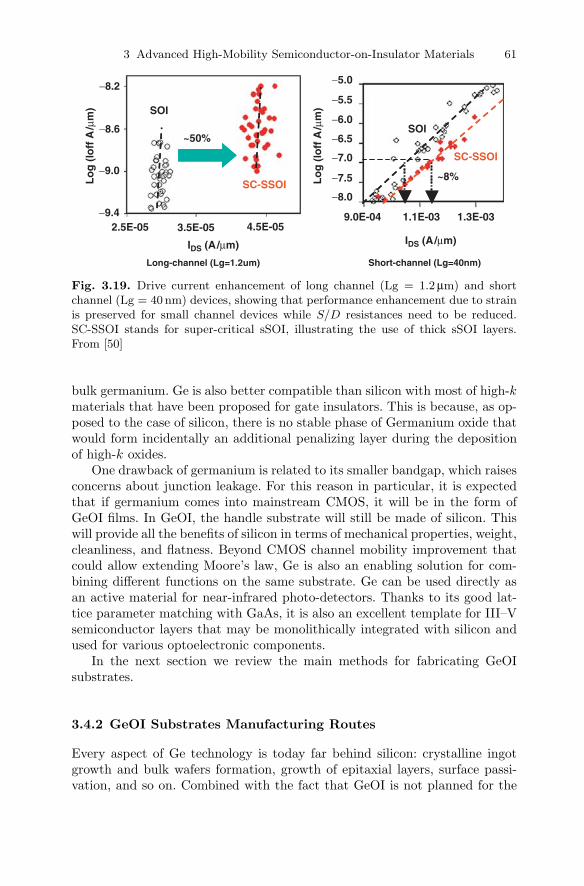
3 Advanced High-Mobility Semiconductor-on-Insulator Materials 61
Long-channel (Lg=1.2um)
Lo
g (
loff
A/µ
m)
Lo
g (
loff
A/µ
m)
−8.2 −5.0
−5.5
−6.0
−6.5
−7.0
−7.5
−8.0
2.5E-05 3.5E-05 4.5E-059.0E-04 1.1E-03 1.3E-03
IDS (A/µm) IDS (A/µm)
−8.6
−9.0
−9.4
Short-channel (Lg=40nm)
SOI
~50%
SC-SSOI
SOI
SC-SSOI
~8%
Fig. 3.19. Drive current enhancement of long channel (Lg = 1.2 µm) and shortchannel (Lg = 40 nm) devices, showing that performance enhancement due to strainis preserved for small channel devices while S/D resistances need to be reduced.SC-SSOI stands for super-critical sSOI, illustrating the use of thick sSOI layers.From [50]
bulk germanium. Ge is also better compatible than silicon with most of high-kmaterials that have been proposed for gate insulators. This is because, as op-posed to the case of silicon, there is no stable phase of Germanium oxide thatwould form incidentally an additional penalizing layer during the depositionof high-k oxides.
One drawback of germanium is related to its smaller bandgap, which raisesconcerns about junction leakage. For this reason in particular, it is expectedthat if germanium comes into mainstream CMOS, it will be in the form ofGeOI films. In GeOI, the handle substrate will still be made of silicon. Thiswill provide all the benefits of silicon in terms of mechanical properties, weight,cleanliness, and flatness. Beyond CMOS channel mobility improvement thatcould allow extending Moore’s law, Ge is also an enabling solution for com-bining different functions on the same substrate. Ge can be used directly asan active material for near-infrared photo-detectors. Thanks to its good lat-tice parameter matching with GaAs, it is also an excellent template for III–Vsemiconductor layers that may be monolithically integrated with silicon andused for various optoelectronic components.
In the next section we review the main methods for fabricating GeOIsubstrates.
3.4.2 GeOI Substrates Manufacturing Routes
Every aspect of Ge technology is today far behind silicon: crystalline ingotgrowth and bulk wafers formation, growth of epitaxial layers, surface passi-vation, and so on. Combined with the fact that GeOI is not planned for the
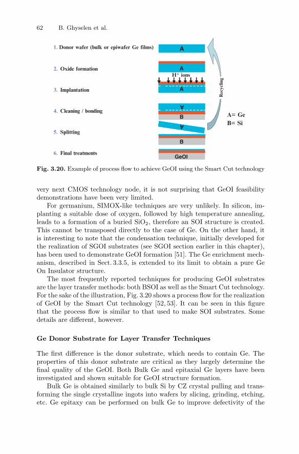
62 B. Ghyselen et al.
A= Ge B= Si
1. Donor wafer (bulk or epiwafer Ge films)
2. Oxide formation
3. Implantation
4. Cleaning / bonding
5. Splitting
6. Final treatments
A
AA
A
H+ ions
AAA
B
AAA
A
B
A
B
Rec
yclin
g
GeOI
Fig. 3.20. Example of process flow to achieve GeOI using the Smart Cut technology
very next CMOS technology node, it is not surprising that GeOI feasibilitydemonstrations have been very limited.
For germanium, SIMOX-like techniques are very unlikely. In silicon, im-planting a suitable dose of oxygen, followed by high temperature annealing,leads to a formation of a buried SiO2, therefore an SOI structure is created.This cannot be transposed directly to the case of Ge. On the other hand, itis interesting to note that the condensation technique, initially developed forthe realization of SGOI substrates (see SGOI section earlier in this chapter),has been used to demonstrate GeOI formation [51]. The Ge enrichment mech-anism, described in Sect. 3.3.5, is extended to its limit to obtain a pure GeOn Insulator structure.
The most frequently reported techniques for producing GeOI substratesare the layer transfer methods: both BSOI as well as the Smart Cut technology.For the sake of the illustration, Fig. 3.20 shows a process flow for the realizationof GeOI by the Smart Cut technology [52, 53]. It can be seen in this figurethat the process flow is similar to that used to make SOI substrates. Somedetails are different, however.
Ge Donor Substrate for Layer Transfer Techniques
The first difference is the donor substrate, which needs to contain Ge. Theproperties of this donor substrate are critical as they largely determine thefinal quality of the GeOI. Both Bulk Ge and epitaxial Ge layers have beeninvestigated and shown suitable for GeOI structure formation.
Bulk Ge is obtained similarly to bulk Si by CZ crystal pulling and trans-forming the single crystalline ingots into wafers by slicing, grinding, etching,etc. Ge epitaxy can be performed on bulk Ge to improve defectivity of the

3 Advanced High-Mobility Semiconductor-on-Insulator Materials 63
active layer. For instance the so-called “Crystal Originated Particles” (COPs),those defects originating from the crystal ingot growth by agglomeration ofvacancies can be eliminated. Much more challenging is Ge heteroepitaxy onstandard silicon substrates; its purpose is to avoid Ge bulk substrates. Thiswould make easier to fabricate large diameter GeOI wafers which will beneeded in the advanced CMOS world (300 mm and beyond). In the lattercase, however, the large lattice mismatch between Ge and Si tends to gen-erate high dislocation densities [54]. Currently, advantages and drawbacks ofthese two approaches are balanced. For some parameters epitaxial germa-nium may be preferred (low COP densities, compatibility with large diameterwafers) while for others bulk is better (fewer dislocations and improved waferflatness). Depending on the success of future developments in this field, oneof these methods may acquire a clear advantage.
Ge Layer Transfer
Layer transfer techniques to process Ge layers exist, but need further opti-mization. Layer splitting by the Smart Cut technology has been demonstrated.Compared to Smart Cut in silicon it has been shown that the correspondingprocess window, as defined by the implantation conditions for splitting, isslightly different [52].
Buried Insulator for GeOI
In SOI substrates, the buried oxide is typically thermally grown on silicon.This provides good bonding properties and ensures that the oxide and itsinterface with the active SOI layer are of high quality, which is critical for thegood electrical behavior of the transistors. This strategy cannot be transferreddirectly to GeOI. Lack of thermally stable Ge oxides and of proper electricalpassivation of a Ge interface are the main impediments. It is expected thatsolutions developed for gate stacks (nitridation, high-k) may eventually beadopted also for the back gate of GeOI channels, which is defined during theGeOI substrate fabrication. In the meantime, temporary solutions have beenexplored to demonstrate prototypes of GeOI substrates. These solutions arebased on oxide deposition on Ge or on direct bonding of Ge with thermalSiO2 grown on the Si handle substrate.
Reclaiming Ge Donor Substrates
Germanium substrates are much more expensive than silicon, and the avail-ability of raw material for Ge is very limited. Recycling and conserving Ge ma-terial is an important consideration if Ge is ever to move into the mainstreamof CMOS technology. Using layer transfer techniques that enable reclaiming ofthe donor wafers is particularly relevant: the same Ge substrates may be used

64 B. Ghyselen et al.
Fig. 3.21. 200 mm GeOI substrates made respectively from (a) bulk Ge or (b)epitaxial layer Ge donor substrates
as donor wafers to make many GeOI substrates with bulk Si handle wafers.The Smart Cut technology is particularly suitable for multiple reuses of thedonor wafers, as it does not sacrifice the donor wafer as in the BSOI approach.
Examples of GeOI Substrates Demonstrations
Figure 3.21 shows the top view of two 200 mm GeOI substrates made by theSmart Cut technology; from a Ge bulk donor wafer (Fig. 3.21a) and from anepi layer grown on an Si substrate (Fig. 3.21b). The quality of such substrateshas been characterized. As an example, in Fig. 3.22, we show a TEM cross-section, in which there are no visible dislocations.
3.4.3 Examples of GeOI Substrates Validations at Device Level
GeOI substrates have been used for various device structures and applica-tions. Ge MOSFETs on GeOI are reported in Chap. 4 of this volume (see
Fig. 3.22. Cross-section TEM of two GeOI substrates made by layer transfer froma bulk Ge donor substrate. In case (a), the bonding interface is located within theburied oxide (SiO2/SiO2 bonding). In case (b), the bonding interface is located ontop of the buried oxide at the Ge/SiO2 interface (Ge/SiO2 bonding)

3 Advanced High-Mobility Semiconductor-on-Insulator Materials 65
also [55, 56]), where it is shown that the device properties are similar, es-pecially in terms of mobilities, to results obtained on bulk Ge substrates.Beyond MOSFETs, such GeOI substrates may also be used for III–V semi-conductors growth. As reported by Thomas et al. [57] GaAs HBT structureshave been successfully realized, with excellent crystalline properties. The re-sults also show a gain in terms of thermal management as compared to similarstructures on bulk GaAs, as can be deduced from the suppression of negativeresistance effects. This gain is explained by better thermal conductivity of thesilicon handle of the GeOI as compared to bulk GaAs.
3.5 Long Term Perspectives
Three major enhancements of SOI structures have been reviewed here: (a)optimization of crystalline orientation, (b) use of strained layers and (c) useof germanium instead of silicon films. Each of them is attractive for highperformance device applications. Since these approaches were proposed onlyin the last few years, further process optimization may be required beforecommercial implementation.
Combining some of these approaches in order to further improve the carriermobility is also possible. A few interesting examples are listed below:
1. Combining non-traditional silicon crystal orientation substrates andstrained layers– 45 rotated strained silicon on insulator (45 SGOI and 45 sSOI sub-
strates)– (110) SGOI; (110) sSOI substrates– (100) strained silicon on insulator on (110) bulk (Hybrid oriented and
strained substrates)2. Combining non-traditional crystal orientation and germanium:
– (111) orientation of GeOI3. Combining strained layers and germanium. In this case compressive stress
in Ge improves mobilities:– Compressively strained GeOI, that can be obtained by layer transfer
techniques from strained Ge donor substrates. In this case epitaxiallygrown Ge on silicon (with optional buffer layers) forms appropriatedonor substrates
– SGOI substrates are also excellent templates for growth of compres-sively strained Ge layers on insulator
4. Combining all three enhancements: non-traditional crystal orientationsubstrates with strained layers and germanium:– Misoriented and compressively strained Ge on insulator– Hybrid orientation substrate with compressively strained Ge on (110)
handle silicon substrate

66 B. Ghyselen et al.
There are even more choices if multiple semiconductor layers on insulatorare taken into account. Such stacks can be grown by heteroepitaxy. Of partic-ular interest is a concept called a “dual channel transistor” that has alreadybeen described in literature [58]. It combines tensile strained silicon from sSOIsubstrates for the nMOSFETs with an additional compressively strained Gelayer that is grown in areas where pMOSFETs are placed. Multiple layers canalso be made by repeating layer transfer operations to form complex SOI-likestructures [59].
In addition to the full substrate solutions described above, process-inducedstrain can be added, to reach complete and flexible optimizations of NMOSand PMOS mobility.
3.6 Conclusions
High mobility semiconductor layers combined with SOI architectures arepromising approaches to meet the challenges for CMOS technology outlinedin the ITRS roadmap.
We have reviewed three substrate-level solutions: (a) non-traditional sil-icon crystal orientation substrates, (b) strained silicon layers and (c) ger-manium. In each case, several scenarios are possible, from simple immediateimprovements such as 45 rotated SOI to long term ones such as the intro-duction of germanium. In the intermediate case of strained silicon, we havedescribed two families of strained SOI substrates that have emerged in thelast few years. The first, called SGOI, is characterized by the presence of aburied relaxed SiGe layer within the substrate, which induces and maintainsstrain within the Si layer that is on top of it. In the second, sSOI substratesare Ge-free and the bonding interface alone maintains the strain. Film thick-ness in sSOI wafers can be optimized for either fully-depleted or partiallydepleted devices, while SGOI with its thicker films is primarily suitable forPD applications. We have also given some suggestions on combining multipleenhancements to further improve device performance.
In addition to these substrate solutions, the present industrial success ofprocess-induced strain shall not be forgotten. A reuse of this know-how isindeed to be considered in a catalytic combination of both approaches tofurther improve both N and P type transistors.
Acknowledgments
The authors want to acknowledge the teams of LETI and SOITEC that madethis work possible, as well as collaborations with different partners that includeST, Freescale, ASM, IMEC and UMICORE. This program has been partiallysupported by the French “Reseau Micro-Nanotechnologies (RMNT)” and the

3 Advanced High-Mobility Semiconductor-on-Insulator Materials 67
French “Ministere de l’Industrie”, as well as MEDEA+ 2T101 SILONIS pro-gram.
References
1. M. Yang, M. Ieong, L. Shi, K. Chan, V. Chan, A. Chou, E. Gusev, K. Jenkins,D. Boyd, Y. Ninomiya, D. Pendleton, Y. Surpris, D. Heenan, J. Ott, K. Guarini,C. D’Emic, M. Cobb, P. Mooney, B. To, N. Rovedo, J. Benedict, R. Mo andH. Ng (2003), High performance CMOS fabricated on hybrid substrate Withdifferent crystal orientations, IEDM 2003 Tech. Dig., p. 453
2. H. Sayama, Y. Nishida, H. Oda, T. Oishi, S. Shimizu, T. Kunikiyo, K. Sonoda,Y. Inoue and M. Inuishi, Effect of 〈100〉 channel direction for high performanceSCE immune PMOSFET with less than 0.15 µm gate length, IEDM 1999 Tech.Dig., p. 657
3. T. Matsumoto, S. Maeda, H. Dang, T. Uchida, K. Ota, Y. Hirano, H. Sayama, T.Iwamatsu, T. Ipposhi, H. Oda, S. Maegawa, Y. Inoue and T. Nishimura (2002),Novel SOI wafer engineering using low stress and high mobility CMOSFET with〈100〉 channel for embedded RF/Analog applications, IEDM 2002 Tech. Dig.,paper 27-07
4. T. Komoda, A. Oishi, T. Sanuki, K. Kasai, H. Yoshimura, K. Ohno, M. Iawai, M.Saito, F. Matsuoka, N. Nagashima and T. Noguchi (2004), Mobility improve-ment for 45 nm node by combination of optimized stress control and channelorientation design, IEDM 2004 Tech. Dig., paper 9.3.1
5. K. Uchida, R. Zednik, C.-H. Lu, H. Jagannathan, J. Mc Vittie, P.C. McIntyreand Y. Nishi (2004), Experimental study of biaxial and uniaxial strain effects oncarrier mobility in bulk and ultrathin body SOI MOSFETs, IEDM 2004 Tech.Dig., paper 9.6.1
6. G.K. Celler and S. Cristoloveanu (2003), Frontiers of silicon-on-insulator, J.Appl. Phys., Vol. 93, no. 9, p. 4955
7. S.M. Sze, Physics of Semiconductor Devices, Wiley, New York (1981), ModernSemiconductor Device Physics, Wiley, New York (1998)
8. K.K. Bourdelle, T. Akatsu, N. Sousbie, F. Letertre, D. Delprat, E. Neyret, N.Ben Mohamed, G. Suciu, C. Lagahe-Blanchard, A. Beaumont, A.-M. Charvet,A.-M. Papon, N. Kernevez, C. Maleville and C. Mazure (2004), Smart CutTM
Transfer of 300 mm (110) and (100) Si Layers for Hybrid Orientation Technology,IEEE Intern. SOI Conf. 2004, p. 98
9. H. Irie, K. Kita, K. Kyuno and A. Toriumi (2004), In-plane mobility anisotropyand universality under uni-axis strains in n- and p-MOS inversion layers on(100), (110) and (111) Si layers, IEDM 2004 Tech. Dig., paper 9.5.1
10. M.V. Fischetti and S.E. Laux (1996), Band structure, deformation potentials,and carrier mobility in strained-Si, Ge, and SiGe alloys, J. Appl. Phys. Vol. 80,no. 4, p. 2234
11. J. Welser, J.L. Hoyt, S. Takagi and J.F. Gibbons (1994), Strain dependence ofthe performance enhancement in strained –Si n-MOSFETs, IEDM 1994 Tech.Dig., p. 373
12. M.D. Giles, M. Armstrong, C. Auth, S.M. Cea, T. Ghani, T. Hoffman, R. Kotl-yar, P. Matagne, K. Mistry, R. Nagisetty, B. Obradovic, R. Shaheed, L. Shifren,

68 B. Ghyselen et al.
M. Stetler, S. Tyagi, X. Wang, C. Weber and K. Zawadzki (2004), Proc. Symp.2004 VLSI Tech., p. 118
13. C. Mazure and I. Cayrefourcq, Status of device mobility enhancement throughstrain silicon engineering, IEEE Intern. SOI Conf. 2005, p. 1
14. T. Ghani, M. Armstrong, C. Auth, M. Bost, P. Charvat , G. Glass, T.Hoffmann, K. Johnson, C. Kenyon, J. Klaus, B. McIntyre, K. Mistry, A. Murthy,J. Sandford, M. Silberstein, S. Sivakumar, P. Smith, K. Zawadzki, S. Thomp-son and M. Bohr (2003), High volume manufacturing logic technology featuringnovel 45 nm gate length strained silicon CMOS transistors, IEDM 2003 Tech.Dig., p. 978
15. G. Scott, J. Lutze, M. Rubin, F. Nouri and M. Manley, IEDM 1999 Tech. Dig.,p. 827
16. H. Sayama, Y. Nishida, H. Oda, T. Oishi, S. Shimizu, T. Kunikiyo, K. Sonoda,Y. Inoue and M. Inuishi, IEDM 1999 Tech. Dig., p. 657
17. T. Sanuki, A. Oishi, Y. Morimasa, S. Aota, T. Kinoshita, R. Hasumi, Y.Takegawa, K. Isobe, H. Yoshimura, M. Iwai, K. Sunouchi and T. Noguchi, Scal-ability of strained silicon CMOSFET and high drive current enhancement inthe 40 nm gate length technology, IEDM 2003 Tech. Dig., p. 65
18. C. Ge, C. Lin, C. Ko, C. Huang, Y. Huang, B. Chan, B. Perng, C. Sheu, P.Tsai, L. Yao, C. Wu, T. Lee, C. Chen, C. Wang, S. Lin, Y. Yeo and C. Hu,Process-strained Si (PSS) CMOS technology featuring 3D strain engineering,IEDM 2003 Tech. Dig., p. 73
19. T. Komoda, A. Oishi, T. Sanuki, K. Kasai, H. Yoshimura, K. Ohno, M. Iwai, M.Saito, F. Matsuoka, N. Nagashima and T. Noguchi, Mobility improvement for45 nm node by combination of optimized stressand channel orientation design,IEDM 2004 Tech. Dig., p 217.
20. A. Steegen, M. Stucchi, A. Lauwers and K. Maex, Silicide induced pattern den-sity and orientation dependent transconductance in MOS transistors, IEDM1999 Tech. Dig., p. 497
21. V. Chan, R. Rengarajan, N. Rovedo, W. Jin, T. Hook, P. Nguyen, J. Chen,E. Nowak, X. Chen, D. Lea, A. Chakravarti, V. Ku, S. Yang, A. Steegen, C.Baiocco, P. Shafer, H. Ng, S. Huang and C. Wann, High speed 45 nm gatelength CMOSFETs integrated into a 90 nm bulk technology incorporating strainengineering, IEDM 2003 Tech. Dig., p. 77
22. H.S. Yang, R. Malik, S. Narasimha, Y. Li, R. Divakaruni, P. Agnello, S. Allen, A.Antreasyan, J.C. Arnold, K. Bandy, M. Belyanski, A. Bonnoit, G. Bronner, V.Chan, X. Chen, Z. Chen, D. Chidambarrao, A. Chou, W. Clark, S.W. Crowder,B. Engel, H. Harifuchi, S.F. Huang, R. Jagannathan, F.F. Jamin, Y. Kohyama,H. Kuroda, C.W. Lai, H.K. Lee, W-H. Lee, E.H. Lim, W. Lai, A. Malikkarjunan,K. Matsumoto, A. McKnight, J. Nayak, H.Y. Ng, S. Panda, R. Rengarajan, M.Steigerwalt, S. Subbanna, K. Subramanian, J. Sudijono, G. Sudo, S.-P. Sun, B.Tessier, Y. Toyoshima, P. Tran, R. Wise, R. Wong, I.Y. Yang, C. II. Wann, L.T.Su, M. Horstmann, Th. Feudel, A. Wei, K. Frohberg, G. Burbach, M. Gerhardt,M. Lenski, R. Stephan, K. Wieczorek, M. Schaller, H. Salz, J. Hohage, H. Ruelke,J. Klais, P. Huebler, S. Luning, R. van Bentum, G. Grasshoff, C. Schawn, E.Ehrichs, S. Goad, J. Buller, S. Krishnan, D. Greenlaw, M. Raab and N. Kepler(2004), Dual stress liner for high performance sub-45 nm gate length SOI CMOSmanufacturing, IEDM 2004 Tech. Dig., p. 75

3 Advanced High-Mobility Semiconductor-on-Insulator Materials 69
23. E.A. Fitzgerald, Y.-H. Xie, M.L. Green, D. Brasen, A.R. Kortan, J. Michel, Y.-J.Mii and B.E. Weir (1991), Totally Relaxed GexSi1-x Layers with low threadingdislocation densities grown on si substrates, Appl. Phys. Lett. 59, p. 811
24. J.M. Hartmann, Y. Bogumilowicz, P. Holliger, F. Laugier, R. Truche, G. Rol-land, M.N. Semeria, V. Renard, E.B. Olshanetsky, O. Estibal, Z.D. Kvon, J.C.Portal, L. Vincent, F. Cristiano and A. Claverie (2004), Reduced pressure chem-ical vapour deposition of SiGe virtual substrates for high mobility devices, Semi-cond. Sci. Technol. 19, p. 311
25. F. Schaffler (1997), High mobility Si and Ge structures, Semiconductor Sci.Techn. 12, p. 1515
26. K.K. Linder, F.C. Zhang, J.-S. Rieh, P. Bhattacharya and D. Houghton (1997),Reduction of dislocation density in mismatched SiGe/Si using a low-temperatureSi buffer layer, Appl. Phys. Lett. 70, p. 3224
27. M. Bauer, K. Lyutovich, M. Oehme, E. Kasper, H.-J. Herzog and F. Ernst(2000), Relaxed SiGe buffers with thicknesses below 0.1 µm, Thin Solid Films369 (2000), p. 152
28. M.T. Bulsara, V. Yang, A. Thilderkvist and E.A. Fitzgerald (1998), GradedInxGa1-xAs/GaA 1.3 µm wavelength light emitting diode structures grown withmolecular beam epitaxy, J. App. Phys. 83, 592
29. S. Takagi, T. Tezuka, N. Sugiyama, T. Mizuno and A. Kurobe (2002), Structureand characteristics of strained-Si-on-insulator (Strained-SOI) MOSFETs, Mat.Res. Soc. Symp. Proc. Vol. 686, p. A1.3.1
30. T. Mizuno, N. Sugiyama, T. Tezuka and S.-I. Takagi (2002), Relaxed SiGe-on-insulator substrates without thick SiGe buffer layer, Appl. Phys. Lett. 80,p. 601
31. T. Tezuka, N. Sugiyama and S. Takagi (2001), Fabrication of strained Si on anultra-thin SiGe-On-Insulator virtual substrate with a high Ge fraction, Appl.Phys. Lett. Vol. 79, p. 1798
32. G. Tarashi, T.A. Langdo, M.T. Currie, E.A. Fitzgerald and D.A. Antoniadis(2002), Relaxed SiGe-on-Insulator fabricated via wafer bonding and etch back,J. Vac. Sci. Technol. B 20, p. 725
33. L.J. Huang, J.O. Chu, D.F. Canaperi, C.P. D’Emic, R.M. Anderson, S.J. Koesterand H.-S. Philip Wong (2001), SiGe-On-Insulator prepared by wafer bondingand layer transfer for high-performance field-effect transistors, Appl. Phys. Lett.78, p. 1267 (2001)
34. B. Ghyselen, C. Aulnette, B. Osternaud, T. Akatsu, C. Mazure, C. Lagahe-Blanchard, S. Pocas, J.-M. Hartmann, P. Leduc, T. Ernst, H. Moriceau, Y.Campidelli, O. Kermarrec, P. Besson, Y. Morand, M. Rivoire, D. Bensahel andV. Paillard (2003), Strained silicon on insulator wafers, Proc. 3rd Intern. Con-ference on SiGe(C) Epitaxy and heterostructures, Santa Fe, 9–12th March 2003
35. B. Ghyselen, J.-M. Hartmann, T. Ernst, C. Aulnette, B. Osternaud, Y. Bogu-milowicz, A. Abbadie, P. Besson, O. Rayssac, A. Tiberj, N. Daval, I. Cayrefourq,F. Fournel, H. Moriceau, C. Di Nardo, F. Andrieu, V. Paillard, M. Cabie, L.Vincent, E. Snoeck, F. Cristiano, A. Rocher, A. Ponchet, A. Claverie, P. Bou-caud, M.-N. Semeria, D. Bensahel, N. Kernevez and C. Mazure (2004), Engi-neering strained silicon on insulator wafers with the Smart CutTM technology,Solid State Electronics (Special issue on strained Si and heterostructures andDevices), 48 (2004), pp. 1285–1296

70 B. Ghyselen et al.
36. B. Hollander, St. Lenk, S. Mantl, H. Trinkaus, D. Kirch, M. Luysberg, T.Hackbarth, H.-J. Herzog and P.F.P. Fichtner (2001), Strain relaxation of pseudo-morphic Si1-xGex/Si(100) heterostructures after hydrogen or helium ion im-plantation for virtual substrate fabrication, Nucl. Instr. Meth. Phys. Res. B175–177, p. 357
37. J.M. Hartmann, A. Abbadie, M. Vinet, L. Clavelier, P. Hollinger, D. Lafond,M.N. Semeria and P. Gentile (2003), Growth kinetics of Si on fullsheet, patternedand silicon-on-insulator substrates, J. Cryst. Growth 257, p. 19
38. T. Mizuno, N. Sugiyama, T. Tezuka, T. Numata and S. Takagi (2003), Highperformance strained-SOI CMOS devices using thin film SiGe-on-insulator tech-nology, IEEE Trans. Electron Devices, vol. 50, p. 988
39. K. Rim, L. Shi, K. Chan, J. Chu, D. Boyd, K. Jenkins, J. Ott, D. Lacey, P.Mooney, M. Cobb, N. Klymko, F. Jamin, S. Koester and T. Kanarsky (2003),Strained Si MOSFETs on bulk and SiGe-on-Insulator (SGOI) substrates, inProc. ISTDM Conf., 2003, p. 9
40. M. Sadaka, A.V.-Y. Thean, A. Barr, D. Tekleab, S. Kalpat, T. White, T.Nguyen, R. Mora, P. Beckage, D. Jawarani, S. Zollner, M. Kottke, R. Liu,M. Canonico, Q-H Xie, X-D Wang, S. Parsons, D. Eades, M. Zavala, B.-Y.Nguyen, C. Mazure and J. Mogab (2004), Fabrication and operation of Sub-50 nm Strained-Si on Si 1-x Ge, on Insulator (SGOI) CMOSFETs, IEEE Intern.SOI Conf. 2004, p. 209
41. F. Andrieu, T. Ernst, O. Faynot, O. Rozeau, Y. Bogumilowicz, J.-M.Hartmann, L. Brevard, A. Toffoli, D. Lafond, H. Dansas, B. Ghyselen, F. Four-nel, G. Ghibaudo and S. Deleonibus (2005), In-depth study of strained SGOInMOSFETs down to 30 nm gate length, Proc. of ESSDERC 2005, Grenoble(FR), p. 297
42. K. Rim, K. Chan, L. Shi, D. Boyd, J. Ott, N. Klymko, F. Cardone, L. Tai,S. Koester, M. Cobb, D. Canaperi, B. To, E. Duch, I. Babich, R. Carruthers,P. Saunders, G. Walker, M. Steen and M. Ieong (2003), Fabrication and mo-bility characteristics of ultra-thin strained Si directly on insulator (SSDOI)MOSFETs, IEDM Tech. Dig. 2003, p. 49
43. T.A. Langdo, A. Lochtefeld, M.T. Currie, R. Hammond, V.K. Yang, J.A. Car-lin, C.J. Vineis, G. Barithwaite, H. Badawi, M.T. Bulsara and E.A. Fitzgerald(2002), Preparation of Novel SiGe-free strained Si on insulator substrates, IEEEIntern. SOI Conf. 2002, p. 211
44. T.S. Drake, C.Ni Chleirigh, M.L. Lee, A.J. Pitera, E.A. Fitzgerald, D.A.Antoniadis, D.H. Anjum, J. Li, R. Hull, N. Klymko and J.L. Hoyt (2003), Fab-rication of ultra-thin strained silicon on insulator, J. Electron. Mat. 32, p. 972
45. I. Cayrefourcq, M. Kennard, F. Metral, C. Mazure, A. Thean, M. Sadaka, T.White and B.Y. Nguyen (2005), Mobility enhancement through substrate engi-neering, Silicon-on-Insulator Technology and Devices XII, ECS Proc. Vol 2005-03, edited by G.K. Celler et al. (The Electrochemical Society, Pennington, NJ,USA, 2005)
46. M. Kennard, C. Figuet, Y.-M. Le Vaillant, F. Triolet, C. Villeneuve, C. Aulnette,C. Berne, L. Portigliati, E. Guiot, N. Daval, R. Larderet, C. Le Moingne, S.Bisson, F. Metral, Z. Chahra, I. Cayrefourcq, C. Mazure, N. Cody, C. Arena andC. Werkhoven (2005), The critical role of epitaxy in the fabrication of enhancedmobility substrates, Proc. 4th International Conference on Silicon Epitaxy andheterostructures (ICSI-4), Awaji island-Hyogo, Japan, 23–26th May 2005

3 Advanced High-Mobility Semiconductor-on-Insulator Materials 71
47. T.A. Langdo, M.T. Currie, Z.-Y. Cheng, J.G. Fiorenza, M. Erdtmann, G.Braithwaite, C.W. Leitz, C.J. Vineis, J.A. Carlin, A. Lochtefeld, M.T. Bulsara,I. Lauer, D.A. Antoniadis and M. Somerville (2004), Strained Si on insulatortechnology: from materials to devices, Solid State Electronics (special issue onstrained Si and heterostructures and Devices), 48 (2004), pp. 1357–1367
48. I. Lauer, T.A. Langdo, Z.-Y. Cheng, J.G. Fiorenza, G. Braithwaite, M.T.Currie, C.W. Leitz, A. Lochtefeld, H. Badawi, M.T. Bulsara, M. Somerville andD.A. Antoniadis (2004), Fully depleted n-MOSFETs on Supercritical ThicknessStrained SOI, IEEE Elect. Dev. Lett., Vol. 25, No. 2, p. 83
49. F. Andrieu, T. Ernst, O. Faynot, Y. Bogumilowicz, J.-M. Hartmann, J. Eymery,D. Lafond, Y.-M. Levaillant, C. Dupre, R. Powers, F. Fournel, C. Fenouillet-Beranger, A. Vandooren, B. Ghyselen, C. Mazure, N. Kernevez, G. Ghibaudoand S. Deleonibus (2005), Co-integrated dual strained channels on fully depletedsSDOI, IEEE Intern. SOI Conf. 2005, “late news”
50. A.V.Y. Thean, T. White, M. Sadaka, L. McCormick, M. Ramon, R. Mora, P.Beckage, M. Canonico, X.-D. Wang, S. Zollner, S. Murphy, V. Van Der Pas,M. Zavala, R. Noble, O. Zia, L-G. Kang, V. Kolagunta, N. Cave, J. Cheek, M.Mendicino, B.Y. Nguyen, M. Orlowski, S. Venkatesan, J. Mogab, C.H. Chang,Y.H. Chiu, H.C. Tuan, Y.C. See, M.S. Liang, Y.C. Sun, I. Cayrefourcq, F.Metral, M. Kennard and C. Mazure (2005), Performance of super-criticalstrained-Si directly on insulator (SC-SSOI) CMOS based on high-performancePD-SOI technology, Proc. Symp. 2005 VLSI Tech, p. 134
51. S. Nakaharai, T. Tezuka, N. Sugiyama, Y. Moriyama and S.-I. Takagi (2003),Characterization of 7-nm-thick strained Ge-on-insulator layer fabricated by Ge-condensation technique, Appl. Phys. Lett., vol. 83, no. 17, p. 3516
52. C. Deguet, C. Morales, J. Dechamp, J.M. Hartmann, A.M. Charvet, H.Moriceau, F. Chieux, A. Beaumont, L. Clavelier, V. Loup, N. Kernevez,G. Raskin, C. Richtarch, F. Allibert, F. Letertre and C. Mazure (2004),Germanium-On-Insulator (GeOI) structures realized by the Smart Cut TM tech-nology, IEEE Intern. SOI Conf. 2004, p. 96
53. T. Akatsu, C. Deguet, C. Richtarch, F. Letertre, L. Sanchez, N. Kernevez, L.Clavelier, C. Le Royer, J.M. Hartmann, V. Loup, M. Meuris, B. De Jaeger andG. Raskin (2005), 200 mm Germanium On Insulator (GeOI) by Smart Cuttechnology and recent GeOI pMOSFETs achievements, IEEE Intern. SOI Conf.2005, p. 137
54. J.M. Hartmann, J.-F. Damlencourt, Y. Bogumilowicz, P. Hollinger, G. Rollandand T. Billon (2005), Reduced pressure-chemical vapor deposition of intrinsicand doped Ge layers on Si(001) for microelectronics and optoelectronics pur-poses, J. Cryst. Growth, 274, p. 90
55. B. De Jaeger, R. Bonzom, F. Leys, O. Richard, J. Van Steenbergen, G. Wind-erickx, E. Van Moorhem, G. Raskin, F. Letertre, T. Billon, M. Meuris and M.Heyns (2005), Optimisation of a thin epitaxial Si layer as Ge passivation layerto demonstrate deep sub-micron n- and p-FETs on Ge-On-Insulator substrates,M. Eng., 80 (2005), p. 26
56. L. Clavelier, C. Le Royer, C. Tabone, J.M. Hartmann, C. Deguet, V. Loup, C.Ducruet, C. Vizioz, M. Pala, T. Billon, F. Letertre, C. Arvet, Y. Campidelli, V.Cosnier and Y. Morand (2005), Fully Depleted Germanium p-MOSFETs withHigh-K and metal gate fabricated on 200mm GeOI substrates, ProceedingsSilicon Nanoelectronics Workshop, June 2005, Kyoto, Japan

72 B. Ghyselen et al.
57. S.G. Thomas, E.S. Johnson, C. Tracy, P. Maniar, X. Li, B. Roof, Q. Hartmannand D.A. Ahmari (2005), Fabrication and characterization of InGaP/GaAs het-erojunction bipolar transistors on GOI substrates, IEEE Electr. Dev. Lett., Vol.26, no. 7, J 2005, p. 438
58. M.L. Lee and E.A. Fitzgerald (2003), Optimized strained Si/strained Ge dualchannel heterostructures for high mobility p- and n-MOSFETs, IEDM 2003Tech. Dig., p. 429
59. B. Ghyselen (2003), Advanced SOI structures based on wafer bonding: Ashort review, Wafer Bonding VII : Science, Technology and Applications, ECSProceedings (PV 2003-19, ISBN 1-56677-402-0), Pennington, NJ (2003)

4
Passivation and Characterization ofGermanium Surfaces
S.R. Amy and Y.J. Chabal
Summary. This chapter reviews the chemical passivation of germanium surfacesachieved in a variety of environments (ultra high vacuum or UHV, gas and liquidphases). The UHV studies make it possible to better control the chemical nature ofsurface termination and to study the resulting structure and bonding geometries.Gas phase or vapor processing helps span a larger pressure range, sometimes impor-tant to achieve thin film growth (e.g., nitridation). Finally, wet chemical treatmentsare attractive for large industrial batch processing. They remain, however, the mostdifficult methods to fully control germanium passivation. For that reason, emphasisis given to understanding how various experimental characterization techniques canbest study germanium surfaces in all these environments, and to summarizing thebest current processing conditions.
4.1 Introduction
As a group IV semiconductor, germanium (Ge) is expected to display manyof the same properties as silicon (Si). Yet, despite its better bulk electricalperformances (higher hole and low-field mobilities, and narrower bandgap) [1],Ge has not been used much in the past because its oxide is much less stablethan SiO2. As a result, the electrical properties of the Ge/GeOx interfaceare much worse than for Si/SiO2, where x is used to emphasize that GeO2
is not necessarily the dominant oxide form for germanium. The nature ofgermanium oxide is such that wet chemical procedures for cleaning Ge (socritical for device fabrication) have been very challenging to establish. Yet,with renewed interest for high mobility substrates as Si is reaching some ofits fundamental limits, the need to understand and control the passivation ofGe surfaces is even greater.
Key to developing an understanding of surface passivation are surfacecharacterization techniques such as X-ray photoelectron spectroscopy (XPS),Fourier-transform infrared (FTIR) spectroscopy, and scanning tunneling mi-croscopy (STM). The value of these techniques for Ge surfaces is briefly de-scribed in the next section.

74 S.R. Amy and Y.J. Chabal
The chapter is organized as follows: after a brief description of relevantexperimental techniques, the methods for cleaning Ge in an ultra-high vac-uum (UHV) environment are discussed to help understand the fundamentalsurface chemistry of Ge surfaces. The nature of Ge oxide is then consideredas the growth and removal of such oxide is central to proper control of passi-vation. The rest of the chapter deals with surface passivation (i.e., chemicalfunctionalization) using various elements or compounds, including hydrogen,nitride, oxynitride, sulfur, and chlorine, which are all relevant to subsequentprocessing (e.g., high-κ dielectrics growth) on Ge. For each case, the workdone in UHV is presented first, followed by the description of wet chemicalmethods.
4.2 Experimental Methodology
4.2.1 X-ray and UV Photoemission Spectroscopy
X-ray photoemission spectroscopy (XPS) also known as electron spectroscopyfor chemical analysis (ESCA) is most useful to identify elements, and theirchemical environment, in the surface region. Using a source of high-intensitymonochromatic X-ray from a rotating anode, or a synchrotron, XPS is per-formed by detecting photo-emitted electrons and measuring their kinetic en-ergy. The short mean free path of electrons in solids (generally ∼2–100 A)makes XPS a very surface sensitive technique and limits its applicationto films less than 100 A. Some depth resolution is achievable by varyingthe detection angle of the emitted electrons, using grazing emission forhighest surface sensitivity and normal emission for highest bulk contribu-tion. The sensitivity varies with elements, but on average it is ∼1 atom%.For the studies reviewed in this chapter, the relevant core levels are theGe2p and Ge3d, the O1s, the C1s, subject to sensitivity factors given inTable 4.1.
UV photoemission is ideal to study the valence band region, which is moresensitive to surface states and to details of surface chemical bonding. Thistechnique is convenient because it does not rely on synchrotron radiation (asimple UV lamp is sufficient).
Table 4.1. Binding energies and sensitivity factors of Ge2p, Ge3d, O1s and C1s
Element Binding energy (eV) Sensitivity
Ge2p 1248.1/1217Ge3d 29.2/29.8 6.1O1s 543.1 0.66C1s 284.2 0.25

4 Passivation and Characterization of Germanium Surfaces 75
4.2.2 Fourier Transform Infrared Spectroscopy
Infrared (IR) spectroscopy is ideal to probe the chemical nature of surfaces.By identifying molecular vibrations, it makes it possible to infer the chemicalbonding of a variety of species at the surface, including oxides, nitrides, andhalogens. An advantage of IR spectroscopy is its high sensitivity to hydro-gen, which is much harder to detect by XPS or Auger Electron Spectroscopy(AES) for instance. In contrast to XPS, IR spectroscopy requires the use ofa reference surface to eliminate contribution from the bulk. This requirementunderscores the fact that IR spectroscopy, like all other optical methods, is notintrinsically surface sensitive. The biggest challenge consists therefore in usingthe most appropriate reference surface to lower the bulk and other unwantedcontributions as much as possible. Another challenge is to enhance sensitivity,which is sometimes done by using Multiple Internal Reflection (MIR) spec-troscopy (Fig. 4.1a), in which the IR beam is reflected many times on thesurface and therefore traverses long distance (3–10 cm) in the bulk material.
Among the most common electronic semiconductors (e.g., Si, InP, GaAs,SiC), Ge is the best optical substrate with relatively low frequency phonon ab-sorption. It is therefore possible to measure surface modes as low as 700 cm−1
using the MIR geometry, and as low as ∼500 cm−1 using direct transmission(Fig. 4.1b). This makes it possible to detect all oxide and nitride modes usingMIR. Figure 4.1 illustrates the IR beam pathway in the two most commongeometries used to perform IR spectroscopy. MIR is best to study Ge in liquidenvironments, and direct transmission is most convenient for in situ studiesof passivation and growth.
Thin films at surfaces such as oxides and nitrides are characterized by ex-tended phonon modes reflecting the interaction between the individual build-ing blocks (e.g., SiO2, Si3N4). Usually, IR spectroscopy is only sensitive totransverse optical (TO) phonon modes because the electric field of the prob-ing radiation is normal to the direction of propagation (i.e., to its wavevector).However, when probing a thin film at a surface with non-normal incidence,there are components of the electric field (and wavevector) both perpendicularand parallel to the surface, so that both the transverse optical (TO) and longi-tudinal optical (LO) phonons can be excited. The longitudinal optical phononis characterized by a dipole perpendicular to the surface and its frequency isblue shifted due to Coulomb interactions.
a) b)
IR beamout
IR beamout
IR beamin
IR beamin
Fig. 4.1. Schematic representation of (a) MIR and (b) transmission geometries

76 S.R. Amy and Y.J. Chabal
4.2.3 Scanning Tunneling Microscopy
STM is a relatively new technique developed by Binning and Rohrer in theearly 1980s that images electrically conductive surfaces with atomic resolution.When a sharp tip (tungsten, for example) is positioned close to a conductivesurface (so close that the wavefunctions of the closest atom from the tip andthe atom from the surface overlap) and a potential difference is applied be-tween the tip and the surface, a tunneling current can be established. Byvarying either the potential or the tip/surface distance, the tunneling currentvaries reflecting details of the local density of states and surface topography.However, the biggest limitation for STM is the need of a conductive sample.Moreover, although the STM does not need vacuum to operate, it appearsthat for stability purposes as well as surface contamination issues, a UHVenvironment is preferable. Low temperature measurements are also often per-formed to increase both stability and spectral resolution when performingscanning tunneling spectroscopy (STS). Most of the experiments on germa-nium substrates described in this chapter are performed in a UHV chamber(∼10−10 Torr), with typical bias (−1.0 V) and tunneling current (0.5 nA).
4.3 Clean Ge Surfaces
To appreciate the issues associated with Ge cleaning, it is important to con-sider first cleaning in an ultra-high vacuum environment. Several methodshave been used initially based mostly on ion sputtering, thermal annealing orwet chemistry. Ion sputtering with Ne+ or Ag+ leads to near-surface damageand disorder, and therefore requires postannealing. Yet, even if the removalof the oxide is complete after ion sputtering, it appears that the surface isstrongly roughened and cannot be recovered even after annealing [2–4]. Fur-thermore, STM images on those clean sputtered/annealed surfaces show thepresence of carbon contamination as two-dimensional islands and the forma-tion of irregular step edges with a wide distribution of terraces (Fig. 4.2) [4].
Other methods have added an ex situ wet chemical pretreatment to thecleaning sequence, followed by a repetition of Ar+ sputtering and annealing inUHV. After such a process, a homoepitaxial Ge layer is grown at 300–350C.Such a method leads to clean germanium surfaces with almost no defect sitesaside from the steps (arising from miscut) as observed with scanning tunnel-ing microscopy [5]. Because of the ion-sputtering-induced roughening of thesurface, other cleaning methods have been investigated leading to Ge surfacepassivation methods described below.
4.4 Oxidation of Ge Surfaces
Germanium oxide has long been known as more complex and less stablethan silicon oxide. Therefore, much of the early work was dedicated to

4 Passivation and Characterization of Germanium Surfaces 77
Fig. 4.2. STM image of a Ge(100) surface prepared by sputter/anneal cycles(reprinted with permission from [4])
characterizing Ge oxides. In the 1930s, crystals of germanium dioxide wereexamined by Laubergayer et al. [6] who identified the existence of three dif-ferent phases of GeO2, one amorphous and two crystalline (hexagonal andtetragonal). Both the amorphous and hexagonal phases are water soluble, butthe tetragonal one is not. In all cases, the GeO bond is believed to be covalentas suggested by the elementary dipole moment (0.04e for GeO; for referenceSiO is 0.31e). All soluble and insoluble oxide structures have been studiedspectroscopically, using Raman Spectroscopy and Fourier Transform Infrared(FTIR) spectroscopy, and both the longitudinal [Im(−1/ε)] and transversal[Im(ε)] optical modes of GeO2 at 857 and 930 cm−1 (Fig. 4.3) have been iden-tified [7, 8].
The oxidation of Ge(100) and Ge(111) surfaces under UHV conditions hasalso been studied using XPS to identify the various oxidation states [9–11].The XPS data reveal the formation of a +2 oxidation state upon annealing.In the work from Schmeisser et al. [10], the stability of Ge oxides is discussedand compared to that of oxides of other elements close to Ge. Prabhakaranet al. [12, 13] were the first to study wet oxidation processes using both XPSand UPS. They compared the formation and removal of oxides on Ge(100)and Ge(111) using wet chemical treatments and in situ oxidation (i.e., byintroducing oxygen gas directly into the UHV chamber). Focusing on theGe3d, Ge2p and O1s core levels, they showed that a cleaning procedure in-volving a sequential treatment in deionized water (H2O), hydrofluoric acid

78 S.R. Amy and Y.J. Chabal
Fig. 4.3. Comparison of reduced Raman spectra of bulk ν −GeO2 with the experi-mentally determined transverse energy loss function, ε2, and the longitudinal energyloss function Im(−1/ε) (reprinted with permission from [8])
(HF) and hydrogen peroxide (H2O2 : H2O) leads to the formation of bothGeO (in a non-bridged configuration) and GeO2 (Fig. 4.4).
This comprehensive study shows that in situ oxidation in UHV resultsin mostly GeO and some related suboxides, wet chemical oxidation leadsto the formation of a mixture of GeO/GeO2 and suboxides, and native ox-idation in room air produces primarily GeO2. Most of the Ge suboxidesappear to be thermally more stable than both GeO2, requiring annealingtemperatures above 450C for removal, and are not water soluble. These find-ings have been confirmed by Zhang et al. [14] who performed a water dipto remove the 1–2 nm thick native oxide, leaving behind 1–2 A thick film ofGeO and C, the latter presumed to originated from the contamination duringwet chemical treatment. Zhang et al. [14] suggested that the dominant phase

4 Passivation and Characterization of Germanium Surfaces 79
Fig. 4.4. Ge3d (left panel), and Ge2p (middle panel) core level spectra of (a) cleanGe(111), (b) clean Ge(111) exposed to 100 L O2 at 250C, (c) ex situ oxide preparedby dipping the wafer in a mixture of H2O2 and H2O at room temperature, and (d)clean Ge(111) exposed to clean room air for 6 h. The difference spectra (e) = (b−a),(f) = (c − a), and (g) = (d − a) are plotted for the Ge3d core level (left panel),and the fittings used for curves (d) are shown as inset at the top of the left andmiddle panels. Data for O1s core level spectra (right panel) are for (a) clean Ge(111)exposed to 100 L O2 at 250C, (b) Ge(111) dipped in a mixture of H2O2 and H2Oat room temperature, and (c) Ge(111) exposed to clean air for 6 h (reprinted withpermission from [12])
of GeO2 formed in this manner is hexagonal. This GeO2 can be thermallyremoved in UHV, leaving behind a clean, reconstructed Ge(100)2× 1 surface,characterized by the sharp surface state emission of surface dimers. Furtherinvestigations have shown that carbon contamination plays a crucial role asthe Ge–C bond is very strong and difficult to break [14]. In fact, carbon con-tamination is present on the surface (observed through C1s core level in XPS)after any wet chemical treatment, and can only be removed after a 30 minUV-ozone irradiation (Fig. 4.5).
The ozone irradiation treatment leads to the formation of ∼2 nm-thickGeO2 including a 1.5 A suboxide layer at the interface that is strongly de-pendent on the UV-ozone exposure time [14]. This oxide thickness is higherthan reoxidation of a clean Ge sample in air for 24 h. Recent FTIR mea-surements performed in our laboratory show that a 30 min-ozone treatmentusing a UV light produces an oxide similar to a 10 s H2O2-grown oxide, i.e.,GeO2 is formed as evidenced by the appearance of GeO2 LO and TO modes(Fig. 4.6). An analysis using Gaussian fits suggests that Ge O and CHx arenot present in a UV-ozone oxide. In general, the growth of UV-ozone oxideson H/Ge(100) surface seems to be slower than chemical oxidation (Fig. 4.6)suggesting that a denser oxide is formed during UV-ozone treatment. In con-trast, the oxide formed after 12 h reoxidation in air is dominated by suboxidesand CHx species, with no dioxide (Fig. 4.6a).

80 S.R. Amy and Y.J. Chabal
Fig. 4.5. C1s core level spectra from Ge(100) wafers after undergoing (a) a de-greasing step involving successive rinses of trichloroethylene, acetone and methanol(process 1), (b) process 1 followed by a thermal anneal to 620 K, (c) process 1followed by an ultrasound rinse in deionized water for 15min (process 2), (d)process 2 followed by a thermal anneal to 620 K, (e) process 2 followed by a 30 minUV/ozone exposure (process 3) and (f) process 3 followed by a thermal anneal to620K (reprinted with permission from [14])
A recent FTIR and XPS study has examined the removal of oxidesprepared by various chemical treatments on epi-ready Ge(100) [15]. The IRspectrum (Fig. 4.7a) obtained after rinsing a native oxide (epi-ready and sub-sequent air exposure) in deionized (DI) water shows the loss (negative ab-sorption) of a broad absorbance feature in the 750–1050 cm−1 range, with amore intense negative component at 785 cm−1. This region generally corre-sponds to germanium oxide, but the assignment is difficult because this bandis wide and relatively featureless. The removal of this oxide in water suggeststhat it consists mostly of GeO2 in either an hexagonal (solubility: 4.5 g l−1)or amorphous (solubility: 5.2 g l−1) phase (Fig. 4.7) [15].
Further treatment in H2O2 leads to the growth of two components at 830and 980 cm−1 indicating the regrowth of an oxide (although the resulting oxideis thinner than the original native oxide since the overall integrated area is stillnegative). This new H2O2-grown oxide is also soluble in water suggesting that

4 Passivation and Characterization of Germanium Surfaces 81
600 800 1000 1200
Abs
orba
nce
Wavenumber (cm−1)
10−3
Ge=O
GeO2
CHx
GeOxa)
b)
c)
=
Fig. 4.6. Transmission absorption IR spectra of germanium oxides formed (a) after90min in air, (b) after 30min UV/ozone exposure and (c) after 10 s in H2O2 (30%).The reference spectrum is H/Ge(100) in all cases (see Sect. 4.55). Gaussian lines areused for the fitting (unpublished results)
500 600 700 800 900 1000 1100 1200 1300
Abs
orba
nce
Wavenumber (cm−1)
700 800 900 1000 1100 1200 1300
10−3
c)
b)
a)
10−4
Ge=O
GeO2TO LO
GeOx
GeO2
700 800 900 1000 1100 1200 1300
=
Fig. 4.7. Transmission absorption IR spectra of Ge(100) after treatment in: (a)deionized H2O, (b) deionized H2O followed by 10 s in H2O2. All the spectra arereferenced to an as-received Ge(100) wafer. The inset shows the oxide region afterH2O2 oxidation, using the H2O-treated Ge(100) surface as reference (reprinted withpermission from [15])

82 S.R. Amy and Y.J. Chabal
it is primarily composed of amorphous or polycrystalline GeO2 [15]. By refer-encing this H2O2-grown oxide to the surface previously treated in water (insetin Fig. 4.7 corresponding to the difference of spectra b and a) it is apparentthat this newly formed oxide is characterized by three distinct componentsat 830, 940 and 980 cm−1. The intensity dependence of these components onthe photon incidence angle (varied from 60 to 10 with respect to the nor-mal) indicates that the pair at 830 and 940 cm−1 exhibits the polarizationdependence expected for the transverse (TO, parallel) and longitudinal (LO,perpendicular) optical phonon modes of GeO2 (involving primarily the Ge–O–Ge asymmetric stretch mode) [7,8]. The TO and LO modes associated withthe Ge–O–Ge symmetric stretch are observable at 583 cm−1 (weak shoulder)and 595 cm−1 respectively. The assignment of the third absorbance feature at980 cm−1 is challenging. Its relatively high frequency points to the existenceof germanium doubly-bonded to oxygen (Ge O). Its dependence on the in-cidence angle indicates that it is mostly but not completely perpendicular tothe surface (Fig. 4.8).
XPS data(15) confirm the presence of GeO and GeO2 and are in completeagreement with the data from Prabhakaran et al. [12] and Zhang et al. [14].Using a simple attenuation layer model and assuming a 15 A mean free pathfor the photoelectrons, the total native oxide thickness is estimated to be∼15 ± 5 A. The GeO2 component completely disappears after DI H2O rinseand only GeO remains on the surface [15]. Longer rinse time in DI water does
900600 700 800 1000 1100 1200 1300
Abs
orba
nce
Wavenumber (cm−1)
Ge=O2.10−4
60°
10°
TO LO
GeO2
Fig. 4.8. Transmission absorption IR spectra of Ge(100) after H2O, H2O2 chemicaltreatment for two incidence angles: 10 and 60 with respect to the normal. Thereference spectra are H2O-treated Ge(100) (unpublished results)
4 Passivation and Characterization of Germanium Surfaces 83
not remove GeO [16]. Hydrogen peroxide grows a mixture of GeO and GeO2
oxides very similar to the initial oxides present on the as-received substrates.Using the same approach as for the as-received samples, we estimate the H2O2
oxide to be about 10 A thick [14].
4.5 Hydrogenation of Germanium Surfaces
4.5.1 Hydrogenation in Ultra High Vacuum
Hydrogenation of clean germanium surfaces was first performed using atomichydrogen. In 1963, Becker and Gobeli [17] pioneered the use of multi-ple internal reflection to examine hydrogen chemisorption on silicon. Later,UHV/FTIR studies of hydrogen adsorption on both Si(100)-(2× 1) andGe(100)-(2× 1) gave clear evidence for the formation of both mono-, di- andtri-hydrides on Si(100) but primarily monohydride on Ge(100) [18], as laterconfirmed by STM studies. Specifically, surface IR spectra as a function ofthe hydrogen coverage show the presence of two absorbance components at1,979 and 1,991 cm−1 oriented parallel and perpendicular to the surface, re-spectively, corresponding to the asymmetric and symmetric stretch modes ofthe monohydride structure (Fig. 4.9). Only at high exposures can spectralcomponents associated with dihydride be observed, but they remain weakerthan for comparable exposures on Si(100). At very low coverage, the hydro-gen atoms are randomly distributed and there is evidence that most of thedangling bonds are initially unpaired [18].
Later STM studied confirmed that, the (2× 1) reconstruction is pre-served [11, 18–22] as a stable monohydride phase after moderate atomic Hexposures at room temperature (Fig. 4.10) [19, 20, 22]. Prolonged exposuresat room temperature leads to the development of line defects, involving theformation of GeH2 rows with local H/Ge(100)-(3× 1) arrangement, while alocal (2× 1) reconstruction still dominates. The GeH2 structure is unstableand can easily be reduced to monohydride because of collision-induced H2
desorption or by dissociation (Fig. 4.11) [22].At substrate temperatures higher than 400 K, hydrogenation of Ge(100)-
(2× 1) results in etching. Single atoms and dimer vacancies are formed, fol-lowed by line defects along the germanium dimer row, which leads to theformation of V-groove-shaped etch pits (Fig. 4.12) [20]. GeH2 formation isan essential first step in the etching process because it initiates Ge-Ge bondbreaking. Etching proceed with release of GeH4 gas, which has been detecteddirectly with mass spectrometry [21].
4.5.2 Wet Chemical Treatment of Flat Single CrystalGermanium Surfaces
Several groups have studied the effect of hydrofluoric (HF) acid treatment onchemically grown GeO2 surfaces [15,23–28]. Dependence on HF etching time

84 S.R. Amy and Y.J. Chabal
Fig. 4.9. Multiple internal reflection infrared spectra as a function of H coverageon a flat Ge(100)-(2× 1) surface at room temperature. The exposures are quotedin terms of molecular hydrogen exposures (the actual atomic H exposure are ex-actly proportional and roughly two orders of magnitude lower than the molecularexposures) (reprinted with permission from [18])
and concentration (ranging from 2 to 50%) has been investigated. Few studiesreport complete H-passivation, although most agree that HF does removewet-chemical oxides. The main difficulty of such studies is the lack of directevidence for H termination.
A common procedure consists of multiple cycles consisting of immersionin HF (10 s) and DI water (20 s) repeated five times. Studies of the resultingsurfaces include XPS, second harmonic generation (SHG) and ellipsometryfor Ge(111) and Ge(100). The XPS studies of Deegan et al. [24] report noevidence for the presence of oxide after the above treatment, i.e., no shouldersare observed in the Ge3d and Ge2p core level spectra at higher kinetic energy(Fig. 4.13). However, similar experiments performed by Bodlaky et al. [28]reveal the presence of a non-negligible sub-oxide contribution (∼5 A) on theGe2p core level spectrum, consistent with the observation of the O1s peak(Fig. 4.14).
Using SHG, Bodlaky et al. [28] report that the measured rotationalanisotropy for H–Ge(111) surface is inconsistent with what is expected forthis surface. Namely, since the Ge–O bond is more polar that the Ge–H bond,

4 Passivation and Characterization of Germanium Surfaces 85
Fig. 4.10. Filled-state STM images (15× 15 nm2) of (a) the adsorbate-free Ge(100)-(2× 1) surface and (b) the nearly monohydride-saturated surface (reprinted withpermission from [22])
the SHG-rotational anisotropy pattern for H/Ge and GeO2/Ge should be dif-ferent. The observed similarity of both surfaces, H/Ge and GeO2/Ge, suggeststhat the hydrogen monolayer is either inhomogeneous or defective, i.e., mustcoexist with an oxide layer. The HF-etched surface is also highly unstable,
Fig. 4.11. Schematic diagram for the Ge 2× 1 : H to 3× 1 : H transition andantiphase monohydride dimer row formation (reprinted with permission from [22])

86 S.R. Amy and Y.J. Chabal
(a) (b)
(c) (111)(100)
54.74°2 µm
Fig. 4.12. FE-SEM images of (a) a typical etch pit of V-groove shape formed ona Ge(100) surface exposed to H2(g) of ∼1 × 10⁶ L at T = 400 K, (b) the cross-sectional view of (a) and (c) a schematic diagram of (b) showing that the etch pitsare bounded by a set of four (111) planes (reprinted with permission from [20])
exhibiting a rapid oxidation in air. Specifically, H-terminated Ge(111) sur-faces oxidize quickly without the typical induction period observed for H/Sisurfaces that undergo a very slow initial oxidation. The authors note that athick oxide layer (∼5 A) is formed on H/Ge surfaces and suggest that some
Fig. 4.13. Ge2p3/2 core level of Ge(111) (a) as received, (b) after HF/water etched,(c) etched sample after 1 week in air, (d) etched sample after 1 month in air(reprinted with permission from [24])

4 Passivation and Characterization of Germanium Surfaces 87
Fig. 4.14. Ge2p3/2 and O1s core level spectra of Ge(111) as received (solid line),and after HF/water etched (dashed line ) (reprinted with permission from [23])
oxide already exists on the HF-etched Ge surface. Ellipsometric measurementof the H/Ge(111) surface reveal that the oxide growth in air follows a log-arithmic law [29]. Recent FTIR studies of H/Ge stability in air give strongevidence that hydrocarbon contamination of the surface initially dominates.Within the first hour in air, the growth of a CHx mode is faster than that ofsuboxides (GeOx) (Fig. 4.6 a). After 90 min in air, there is ∼10% of the initialhydrogen coverage left, with relatively little oxide [16].
Another procedure to achieve H-passivation of Ge substrates is to immersea chemically oxidized Ge directly in aqueous HF (10%) for 10 min. Choi etal. [23] first showed that such a procedure did lead to hydrogen-terminationusing FTIR. A hydride termination was clearly derived from the presenceof a broad absorbance features centered at 2,010 cm−1 and corresponding toGeHx stretching modes. The width of the band probably arises from a rela-tively large surface roughness estimated to be ∼3–4 nm after this treatment.For reaction times lower than 10 min in aqueous HF, the authors find thatgermanium surfaces are not fully hydrogenated. For longer reaction times inHF, the hydrogen coverage surprisingly decreases, suggesting a complicatedprocess (Fig. 4.15). More dilute aqueous HF solutions (<10%) also result inincomplete hydrogen-termination (weak GeHx stretch modes) while higherconcentration solution (e.g., 25% HF) leads to surface roughening (8–10 nmas determined by AFM), with deep pitting of the germanium substrate [23].These observations have led the authors to believe that etching can take placejust as it does for Si using higher pH solutions, and that kinetics rather thanthermodynamics dominate during the H-passivation process. A recent studyon the etching effect of different aqueous hydrohalogenic acid solutions onoxidized germanium surfaces clearly shows that high HF concentration (49%)for a short time (5 min) do etch GeO2 and leave suboxides on the surfacethat prevent full hydrogen termination of the germanium surface [25]. Sur-prisingly the authors observe with XPS that longer exposures in HF or otherhydrohalogenic acids do not help in achieving full H passivation.

88 S.R. Amy and Y.J. Chabal
0.004
0.003 c
b
a
d
Abs
orba
nce
0.002
Wavenumber (cm−1)
0.001
0.000
2200 2100 2000 1900 1800
Fig. 4.15. ATR-FTIR spectra of the ν(GeHx) stretching region for the hydrogen-terminated Ge(100) surface prepared by etching with an aqueous 10% HF solution:after (a) 2min, (b) 5min, (c) 10 min, (d) 15 min (reprinted with permission from[23])
A recent FTIR study on chemically oxidized samples (H2O + H2O2) pro-vides a direct measure of the hydrogen coverage after HF etching [15,23–28].Using a transmission geometry instead of ATR to access the full spectral range(400–4,000 cm−1), all the relevant Ge–H modes (bend, scissor, and stretchmodes) are observed. This study shows that etching in 10% HF does lead tothe complete removal of the H2O2-grown germanium oxide (GeO2) as wellas germanium suboxide (GeO) [15], and to full H-termination as mono- anddi-hydrides. Figure 4.16 shows the scissor (834 cm−1) and rocking (640 cm−1)modes of GeH2 together with a broad stretch mode around 2,000 cm−1 at-tributed to Ge-Hx. This broad absorbance feature is composed of unresolvedmodes centered at 1,987, 2,020 and possibly 2,060 cm−1, corresponding to thegermanium mono, di- and tri-hydrides, respectively. An upper limit for thetrihydrides can be set at 10% of the total passivated surface, less than whatis observed on Si. Although a flat Ge(100) surface could in principle supportboth mono- and di-hydrides, with a local 3× 1 reconstruction, the wet etchedsurface is clearly not atomically flat. From the IR spectrum shown in Fig. 4.16,the hydrogen-coverage has been estimated to be around 80% of a monolayer.This partial coverage reflects the poor stability of the HF-etched surface inair as it can be increased by faster transport into the N2-purged spectrometerimmediately after etching.
Complementary XPS information confirms that all oxides and sub-oxidesevident in the Ge3d core level have been removed by HF etching. This isconsistent with the IRAS observation of complete H-termination right afterHF etching. The lack of a well-defined contribution in the O1s core level con-firms the absence of oxide (<0.1 monolayer). However, a careful decomposi-tion of the Ge3d peak reveals the presence of a small component on the higher

4 Passivation and Characterization of Germanium Surfaces 89
600 700 800 1900 2000 2100 2200
Ans
orba
nce
Wavenumber (cm−1)
5.10−5
GeH
GeH2
Stretch mode
GeH2
Bend mode
GeH2
Rock mode
GeH3
Fig. 4.16. Transmission absorption IR spectrum of H/Ge(100) after HF wet chemi-cal treatment for 10min, using the ultra-thin native epiready Ge wafer as reference.The positions for mono-, di- and tri-hydride stretch modes are indicated with verticallines (reprinted with permission from [15])
binding energy side (+1.6 eV with respect to bulk Ge3d). This component can-not be attributed to GeO but it is likely due to the presence of carbon. Sincethe chemical treatment is performed in air, ambient exposure to hydrocarbonsresulting in partial carbon contamination after etching and prior to IRAS orXPS measurements cannot be avoided. In fact, the carbon level detected byXPS is often higher on HF-etched surfaces than on the as-received oxidizedsubstrates or on wet-chemically oxidized surfaces. Figure 4.17 shows, for exam-ple, that the as-received and GeO- or GeO2-terminated surfaces (after H2O orH2O2, respectively) show less carbon contamination. The nature of this carboncontamination is of great interest. There is no doubt that, just as in the caseof hydrophobic H-terminated Si, hydrocarbon molecules can be physisorbedon the surface. In fact, the presence of such hydrocarbons is observed withFTIR with multiple components at 790, 1,440 and 2,800–2,950 cm−1, corre-sponding to deformation and stretching mode of CHx, respectively [16]. Thisobservation suggests that some hydrocarbon molecules react with the germa-nium surface removing H in the process. Direct measurement of Ge–C bondswould greatly help in understanding this contamination process.
4.5.3 Electrochemistry on Flat Single Crystal Germanium Surfaces
Electrochemistry has also been used for hydrogenation and hydroxylationof germanium electrodes [30–34]. Typically, polished flat (111) and (100)germanium substrates are first cleaned with sulfochromic acid/hydrochloric
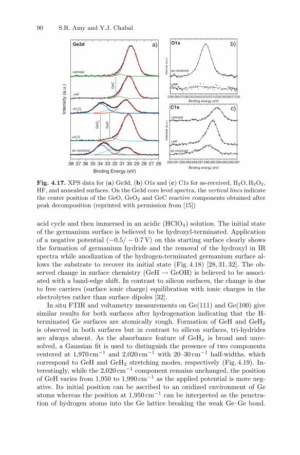
90 S.R. Amy and Y.J. Chabal
38 37 36 35 34 33 32 31 30 29 28 27 26
GeC
GeO
GeO
2
+anneal
+HF
+H2O
2
+H2O
as received
Ge3d
Inte
nsity
(a.
u.)
Binding Energy (eV)
539538537536535534533532531530529528527526
Inte
nsity
(a.
u.)
+HF
as received
O1s
Binding energy (eV)
292291290289288287286285284283282281In
tens
ity (
a.u.
)
+anneal
+HF
as received
C1s
Binding energy (eV)
a) b)
c)
Fig. 4.17. XPS data for (a) Ge3d, (b) O1s and (c) C1s for as-received, H2O, H2O2,HF, and annealed surfaces. On the Ge3d core level spectra, the vertical lines indicatethe center position of the GeO, GeO2 and GeC reactive components obtained afterpeak decomposition (reprinted with permission from [15])
acid cycle and then immersed in an acidic (HClO4) solution. The initial stateof the germanium surface is believed to be hydroxyl-terminated. Applicationof a negative potential (−0.5/ − 0.7V) on this starting surface clearly showsthe formation of germanium hydride and the removal of the hydroxyl in IRspectra while anodization of the hydrogen-terminated germanium surface al-lows the substrate to recover its initial state (Fig. 4.18) [28, 31, 32]. The ob-served change in surface chemistry (GeH → GeOH) is believed to be associ-ated with a band-edge shift. In contrast to silicon surfaces, the change is dueto free carriers (surface ionic charge) equilibration with ionic charges in theelectrolytes rather than surface dipoles [32].
In situ FTIR and voltametry measurements on Ge(111) and Ge(100) givesimilar results for both surfaces after hydrogenation indicating that the H-terminated Ge surfaces are atomically rough. Formation of GeH and GeH2
is observed in both surfaces but in contrast to silicon surfaces, tri-hydridesare always absent. As the absorbance feature of GeHx is broad and unre-solved, a Gaussian fit is used to distinguish the presence of two componentscentered at 1,970 cm−1 and 2,020 cm−1 with 20–30 cm−1 half-widths, whichcorrespond to GeH and GeH2 stretching modes, respectively (Fig. 4.19). In-terestingly, while the 2,020 cm−1 component remains unchanged, the positionof GeH varies from 1,950 to 1,990 cm−1 as the applied potential is more neg-ative. Its initial position can be ascribed to an oxidized environment of Geatoms whereas the position at 1,950 cm−1 can be interpreted as the penetra-tion of hydrogen atoms into the Ge lattice breaking the weak Ge–Ge bond.

4 Passivation and Characterization of Germanium Surfaces 91
Fig. 4.18. IR spectra as a function of potential for Ge(100) surface (p-polarization);top figure: cathodic scan and bottom figure: anodic scan. The reference is taken atthe upper potential bound (reprinted with permission from [31])
Electrochemical incorporation of hydrogen in Ge(111) has been reported ear-lier after a prolonged cathodic treatment [34]. FTIR experiments as a functionof polarization clearly support the penetration of the hydrogen into the Gebulk as the position of the observed band red-shifts while the intensity of the s-and p-polarization remains unchanged: a thin disordered highly hydrogenatedlayer is thus formed close to the surface [34].
The combined voltametry and FTIR data also suggest the possible exis-tence of (111) microfacetting for Ge(100) as an explanation for the observedintensity changes of the GeHx stretch mode. The voltametric peaks (β and α)appear to be associated with hydrogenation of microfacets and steps generat-ing GeH and GeH2.
4.5.4 Electrochemistry on Porous Germanium Substrate
Electrochemical hydrogenation of porous material is natural since it repre-sents an intrinsic step of their formation. Porous materials have been stud-ied extensively because of their photoluminescence properties important foroptoelectronics [35, 36]. Two procedures have been reported. The first oneinvolves an anodic etch of the c-Ge(100) substrate in a 50 wt.% HF solution

92 S.R. Amy and Y.J. Chabal
Fig. 4.19. Analysis of the νGeHx spectrum for Ge (a) (100) and (b) (111), for s-and p-polarization at −0.825 Vsce. The data exhibit evidence for two contributions,with distinct polarization dependences. The dotted curves show the fitting curves(reprinted with permission from [31])
in presence of an halogen lamp (500 W). The second process is based on abipolar electrochemical etching (BEE) technique, whereby the single crys-talline Ge(100) substrate is first cleaned in an ethanoic HCl solution andthen anodized for 5 min, followed by a cathodization step for 1 min. Bothmethods lead to similar H-termination, characterized by a broad stretch modeat ∼2,030 cm−1 corresponding to Ge–Hx (Fig. 4.20) and by GeH2 deforma-tion modes observed at 580 and 830 cm−1 [35, 36]. Little characterization ofgermanium prepared with the anodic etching method has been performed.For H-terminated porous germanium prepared by BEE, the starting surfaceis probably hydroxyl-terminated and becomes hydrogen terminated when apositive potential is applied. The Ge–Ge bonds are protonated upon cath-odization leading eventually to the formation of GeH4 and the dissolutionof the germanium bulk. This results in both hydrogenation and formationof pores. The observed etching process is in fact close to what is observedwhen Ge(100)-2× 1 surfaces are exposed to H2(g) at 400 K [35, 36]. FTIRmeasurements of this porous substrate reveal a broad Ge–H stretching bandwith two components at 2,044 and 2,015 cm−1, i.e., higher in frequency thanusually measured. Choi and Buriak [35] suggest that all forms of hydrides
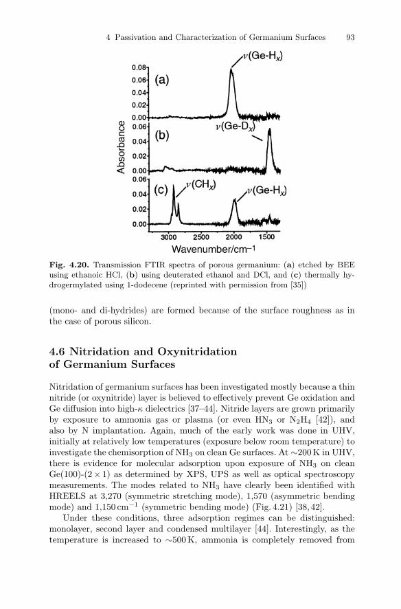
4 Passivation and Characterization of Germanium Surfaces 93
Fig. 4.20. Transmission FTIR spectra of porous germanium: (a) etched by BEEusing ethanoic HCl, (b) using deuterated ethanol and DCl, and (c) thermally hy-drogermylated using 1-dodecene (reprinted with permission from [35])
(mono- and di-hydrides) are formed because of the surface roughness as inthe case of porous silicon.
4.6 Nitridation and Oxynitridationof Germanium Surfaces
Nitridation of germanium surfaces has been investigated mostly because a thinnitride (or oxynitride) layer is believed to effectively prevent Ge oxidation andGe diffusion into high-κ dielectrics [37–44]. Nitride layers are grown primarilyby exposure to ammonia gas or plasma (or even HN3 or N2H4 [42]), andalso by N implantation. Again, much of the early work was done in UHV,initially at relatively low temperatures (exposure below room temperature) toinvestigate the chemisorption of NH3 on clean Ge surfaces. At ∼200K in UHV,there is evidence for molecular adsorption upon exposure of NH3 on cleanGe(100)-(2× 1) as determined by XPS, UPS as well as optical spectroscopymeasurements. The modes related to NH3 have clearly been identified withHREELS at 3,270 (symmetric stretching mode), 1,570 (asymmetric bendingmode) and 1,150 cm−1 (symmetric bending mode) (Fig. 4.21) [38,42].
Under these conditions, three adsorption regimes can be distinguished:monolayer, second layer and condensed multilayer [44]. Interestingly, as thetemperature is increased to ∼500K, ammonia is completely removed from

94 S.R. Amy and Y.J. Chabal
Fig. 4.21. HREELS spectra of NH3 on Ge(100)-(2× 1). The lower curve showsGe(100) exposed to 10 L of NH3 at T = 180 K. The upper curve was taken afterannealing the sample at 473 K for 2min and then cooling the sample back down to180K (reprinted with permission of [42])
the surface (Fig. 4.22) [38]. Since there is no observable spectroscopic featuresrelated to NH2 throughout the whole temperature range, it was concludedthat NH3 does not dissociate on Ge(100). This is in contrast to silicon whereNH3 does dissociate into NH2 and H, although it mostly recombines to desorbas NH3 at higher temperatures. On Ge(100), NH3 adsorbs initially on theelectrophilic surface dimer atom (atom lower in the dimer) and produces a(2× 2) reconstruction because it adsorbs in a zig-zag fashion, causing a flip ofthe dimer tilt direction of every second dimer row. In this HREELS study [38],germanium nitride could only be formed after electron irradiation at 110 K,as evidenced by the appearance of a component at ∼800 cm−1.
First-principles pseudopotential calculations have confirmed that NH3 dis-sociation into NH2 + H on Ge(100) is not energetically stable [43]. NH3 gastreatment performed at either room or high temperatures (up to 870 K) doesnot form any nitride layer. Using relatively low pressures, XPS measurementsconfirm that less than 6.3×10¹³ nitrogen atoms/cm2 are observed on Ge(100),yielding an upper limit for the sticking (reaction) of 3× 10⁻⁶ [45]. This valueis consistent with earlier studies [46] of NH3 adsorption at 180 K, which hadderived a sticking coefficient <10−4.
Nitridation requires higher pressures. Early work was performed on a thinevaporated (porous) germanium films. In the presence of a low pressures ofargon, ammonia was observed to dissociate on the Ge film even at roomtemperature [40]. Infrared experiments on a Ge clean film show the pres-ence of the Ge–NH2 deformation mode in the 1,550–1,600 cm−1 region andGe–H stretch mode at 1,920 cm−1 consistent with dissociation into NH2 and
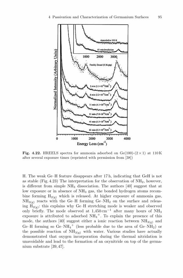
4 Passivation and Characterization of Germanium Surfaces 95
Fig. 4.22. HREELS spectra for ammonia adsorbed on Ge(100)-(2× 1) at 110Kafter several exposure times (reprinted with permission from [38])
H. The weak Ge–H feature disappears after 17 h, indicating that GeH is notas stable (Fig. 4.23) The interpretation for the observation of NH2, however,is different from simple NH3 dissociation. The authors [40] suggest that atlow exposure or in absence of NH3 gas, the bonded hydrogen atoms recom-bine forming H2(g) which is released. At higher exposure of ammonia gas,NH3(g) reacts with the Ge–H forming Ge–NH2 on the surface and releas-ing H2(g): this explains why Ge–H stretching mode is weaker and observedonly briefly. The mode observed at 1,450 cm−1 after many hours of NH3
exposure is attributed to adsorbed NH4+. To explain the presence of this
mode, the authors [40] suggest either a ionic reaction between NH3(g) andGe–H forming so Ge–NH4
+ (less probable due to the area of Ge–NH2) orthe possible reaction of NH3(g) with water. Various studies have actuallydemonstrated that oxygen incorporation during the thermal nitridation isunavoidable and lead to the formation of an oxynitride on top of the germa-nium substrate [39,47].

96 S.R. Amy and Y.J. Chabal
abso
rban
ce1920
1920
1450
1900
.02
1800 1700 1600 1500 1400
1590
f
e
d
c
b
a
Fig. 4.23. IR spectra of ammonia adsorbed on germanium at 300K, 67 Pa (a) after30min, (b) after 4 h, (c) after 17 h. (d)–(f) obtained from separate runs at 665Pa(d) after 30 min, (e) after 2 h30 and (f) pumped for 18 h (reprinted with permissionfrom [40])
Using ellipsometry and optical micrography, Hua et al. [39] have shownthat the growth of a smooth and uniform nitride film takes place at 870–930 Kin 2–4 h on a hydrophobic germanium surface. They also observed an increaseof the refractive index during the growth they attributed to the presence ofoxide [39]. The growth mechanism is dependent on the diffusion of the ni-trogen and oxide into and through the film. However, when nitrogen gas isused instead of ammonia, there is no growth of a nitride layer indicatingthat N2 does not dissociate. Finally, nitridation without oxygen incorporationor carbon contamination has been recently achieved using a plasma-enhancednitridation technique [41]. Auger spectra show that a two-step cleaning proce-dure, involving out-gassing at low temperature and thermal annealing at hightemperature (870 K) in UHV leads to the formation of a good quality nitridelayer (1.6 nm thick) with a stoichiometry close to Ge3N4. Cross-sectional HR-TEM images show a sharp interface between the germanium substrate andthe crystalline Ge3N4 film (Fig. 4.24).
Oxynitridation has been investigated more recently as an alternativeto GeO2 to passivate Ge surfaces. Layers consisting of Ge2N2O are insol-uble in water and their interface with Ge appears to yield good electri-cal properties [48–50]. Oxynitride layers are obtained following a two-stepoxidation/nitridation process: after an ex situ chemical treatment, the hy-drophobic germanium(100) surface is introduced in a furnace at 820 K andmaintained for 90 min in an atmosphere of O2/N2 (1 : 4), followed by NH3
gas flow at 870 K for 30–45 min. TEM pictures of such a films (∼22 nm thick)display a sharp interface between the crystalline germanium and the amor-phous oxynitride layer comparable to a Si/SiO2 interface (Fig. 4.25) [48].However the authors [48] mention that the electron beam stimulates the

4 Passivation and Characterization of Germanium Surfaces 97
Fig. 4.24. A cross-sectional HR-TEM image of Ge3N4/Ge substrate (reprinted withpermission from [41])
decomposition and reaction of the oxynitride layer with the germanium sub-strate, leading to roughening. Oxynitrides have been used as an intermediatelayer for the growth of high-κ dielectrics because they also prevent diffusionof metal species [48,49].
4.7 Sulfur Passivation of Germanium Surfaces
Sulfur has also been investigated as an alternative element to passivate ger-manium surfaces [28,51–55]. Exposure of a clean Ge(100)-(2× 1) surface (ob-tained after various cycles of Ar+ ion sputtering and annealing at 870 K underUHV) to a molecular beam of elementary sulfur leads to the formation of anS/Ge(100)-(1× 1) surface, with ideal Ge–S–Ge (monosulfide) termination [55].XPS data show that there is only one chemical environment for the sulfursurface atoms (Fig. 4.26). The bivalent sulfur atoms are therefore believedto bond in the bridge position between the topmost germanium atoms of the
Ge substrate
Oxynitride
Amorphous Ge cap
20 nm
Fig. 4.25. High resolution TEM image of an oxynitride film grown on a Ge(100)wafer obtained after a two stage-oxidation/nitridation process. The oxynitride layeris capped with amorphous Ge (reprinted with permission from [48])

98 S.R. Amy and Y.J. Chabal
Fig. 4.26. Ge3d core level photoemission spectra for clean and sulfur-coveredGe(100) surfaces. (a) spin orbit splitting and secondary electron background, (b)determination of bulk emission, (c) surface-bulk deconvolution for S/Ge(100)(1× 1)(reprinted with permission [55])
Ge(100) surface: a coverage of one sulfur atom per Ge surface atom is expectedand no sulfur island is present (Fig. 4.27). Local density approximation (LDA)calculations confirm that the dimer bonds are broken with the S adatoms sat-urating the dangling bonds of the top layer Ge atoms restoring the (1× 1)reconstruction with an optimal S–Ge bond length of 2.36 A. In that configu-ration, the total surface energy is lowered by 0.71 eV [52]. The S-terminatedsurface is inert and stable in a UHV environment with no observed contami-nation after 2 days.
Cohen [46], Kuhr [56] and Nelen [51] have used H2S to passivate Ge(100)-(2× 1). They all find that H2S dissociates on a clean Ge(100) into SH, S and Hat room temperature with an S saturation coverage of 0.25 ML. This coveragecan be increased to 0.5 ML by exposing on a substrate at 553 K. This highercoverage is due to hydrogen desorption generating extra sites for HS and Sadsorption.
There has been little work done using wet chemistry. Anderson et al. [54]have used (NH4)2S in a wet chemical treatment similar to that used for GaAs

4 Passivation and Characterization of Germanium Surfaces 99
BROGE SITE
first Ge layer sulfur
2+ 2+ 2+ 2+ 2+ 2+ 2+ 2+ 2+ 2+
2+0+0+0+1+ 2+2+2+
TOP SITE
MONOLAYER ADSORPTION:
SUBMONOLAYER ADSORPTION:
Fig. 4.27. Bridge-site and top-site bonding can be distinguished by the appearanceof the oxidation state 1+ in the case of low-coverage adsorption (reprinted withpermission from [55])
and InP. After a first HF(1%) etching for 1min, the Ge(100) substrate is im-mersed in an aqueous (NH4)2S solution for 20 min at 340 K and rinsed thor-oughly in methanol or water before drying. The surface was then introducedin UHV for LEED and XPS analysis. The surface symmetry is S/Ge(100)-(1× 1) surface similar to what Weser [55] observed on S/Ge(100) obtainedby dosing atomic sulfur on Ge(100)2× 1. However, while the germanium isalso passivated with one layer of bridge-bonded sulfur atoms, the wet chemi-cal preparation leads to trace amounts of oxygen and carbon contamination.In a vacuum environment, sulfur starts to be released from the surface at460 K, and is completely removed by 650–750 K, although a Ge(1× 1) pat-tern is still observed in LEED. Since carbon contamination is observed onthe surface after such an anneal, it is possible that C contamination pre-vents the restoration of a clean Ge(100)-(2× 1) reconstructed surface. Anattractive aspect of the S passivation is the fact that the Ge(100) surfaceremains very flat, even after annealing, with an RMS roughness ranging be-tween 3 and 12 A [54]. The S-passivated surface is believed to be stable inatmosphere, preserving the (1× 1) reconstruction with no trace of oxide. Thisstability is confirmed by Bodlaki et al. [28] who observed with second har-monic generation that no oxidation of an S/Ge(111) surface occurred for up to2 months.
4.8 Chlorine Passivation of Germanium Surfaces
Chlorination of germanium can be achieved using Cl2 gas, both in UHV andat atmospheric pressure, as well as by wet chemistry [57–61]. For instance,the clean Ge(111)-(2× 8) surface was exposed to chlorine gas under ultrahigh vacuum by Citrin et al. [57] who found that the (2× 8) reconstruction

100 S.R. Amy and Y.J. Chabal
111CI
Ge
Fig. 4.28. Schematic view of an ideally chlorine-terminated germanium(111) surface(reprint with permission from [60])
is maintained as the Cl is adsorbed in an atop configuration. Using SEX-AFS, they verified that the reconstruction and Cl coverage are maintainedupon annealing to ∼670K for 5 min, suggesting a good stability of chlorineon germanium surfaces.
Lu et al. [60,61] have shown using XPS that immersion of Ge(111) coveredwith native oxide in dilute aqueous HCl (10%) for 10 min results in a chlorine-passivated germanium surface. Combining XPS to X-ray absorption near edgespectroscopy (XANES), the authors argue that a flat monochloride structureis formed and remains stable in air (Fig. 4.28).
The above studies also show that the orientation of the chemical Ge–Clbond is strictly perpendicular to the surface: the chlorine is bonded to thegermanium substrate in the atop position. These results are in good agreementwith the UHV study performed on the Ge(111)-(2× 8) discussed above [57].A finer analysis using X-ray absorption fine structure (EXAFS) finds a Ge–Clbond of 2.17 nm which is confirmed by theoretical calculations [61]. Multiplescattering clusters and DV-Xα methods show that the Cl–Cl distance has to be4 A to match the Ge(111) lattice constant in order to built a stable Cl/Ge(111)adsorption structure [58]. The observation of Ge–Cl instead of Ge–H uponHCl treatment is explained by Lu et al. [60, 61] by invoking thermodynamicsconsiderations rather than kinetic barriers: the bond energy of Ge–Cl is higherthan Ge–H and is therefore energetically favorable [60]. Unpublished resultsusing FTIR on Ge(100) using the same wet chemical treatment (10% HClfor 10 min) confirm that the germanium oxide and suboxides are completelyremoved with no evidence of Ge–H. Unfortunately, the Ge–Cl stretch mode(350–400 cm−1) cannot be observed directly because it is below the currentdetector sensitivity.
The stability of flat Cl/Ge(111) surfaces has been studied by Bodlakiet al. [28] using SHG and XPS. Their work confirms the absence of oxideas well as suboxides and shows that the surface is unstable as reoxidationoccurs after 1 h in air. (Fig. 4.29): the Ge2p core level starts exhibiting ashoulder at higher binding energy characteristic of GeOx while the inten-sity of the Cl2p core level is decreasing. As observed for H/Ge, the oxide
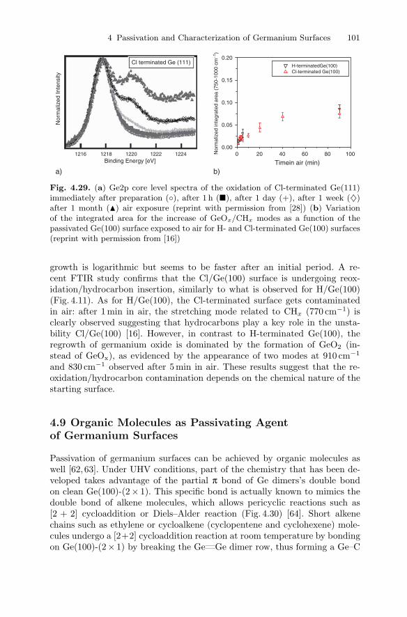
4 Passivation and Characterization of Germanium Surfaces 101
0 20 40 60 80 1000.00
0.05
0.10
0.15
0.20H-terminatedGe(100)Cl-terminated Ge(100)
Nor
mal
ized
inte
grat
ed a
rea
(750
-100
0 cm
−1)
Timein air (min)
Cl terminated Ge (111)N
orm
aliz
ed In
tens
ity
1216 1218Binding Energy [eV]
1220 1222 1224
a) b)
Fig. 4.29. (a) Ge2p core level spectra of the oxidation of Cl-terminated Ge(111)immediately after preparation (), after 1 h (), after 1 day (+), after 1 week (♦)after 1 month () air exposure (reprint with permission from [28]) (b) Variationof the integrated area for the increase of GeOx/CHx modes as a function of thepassivated Ge(100) surface exposed to air for H- and Cl-terminated Ge(100) surfaces(reprint with permission from [16])
growth is logarithmic but seems to be faster after an initial period. A re-cent FTIR study confirms that the Cl/Ge(100) surface is undergoing reox-idation/hydrocarbon insertion, similarly to what is observed for H/Ge(100)(Fig. 4.11). As for H/Ge(100), the Cl-terminated surface gets contaminatedin air: after 1 min in air, the stretching mode related to CHx (770 cm−1) isclearly observed suggesting that hydrocarbons play a key role in the unsta-bility Cl/Ge(100) [16]. However, in contrast to H-terminated Ge(100), theregrowth of germanium oxide is dominated by the formation of GeO2 (in-stead of GeOx), as evidenced by the appearance of two modes at 910 cm−1
and 830 cm−1 observed after 5 min in air. These results suggest that the re-oxidation/hydrocarbon contamination depends on the chemical nature of thestarting surface.
4.9 Organic Molecules as Passivating Agentof Germanium Surfaces
Passivation of germanium surfaces can be achieved by organic molecules aswell [62, 63]. Under UHV conditions, part of the chemistry that has been de-veloped takes advantage of the partial π bond of Ge dimers’s double bondon clean Ge(100)-(2× 1). This specific bond is actually known to mimics thedouble bond of alkene molecules, which allows pericyclic reactions such as[2 + 2] cycloaddition or Diels–Alder reaction (Fig. 4.30) [64]. Short alkenechains such as ethylene or cycloalkene (cyclopentene and cyclohexene) mole-cules undergo a [2+2] cycloaddition reaction at room temperature by bondingon Ge(100)-(2× 1) by breaking the Ge Ge dimer row, thus forming a Ge–C

102 S.R. Amy and Y.J. Chabal
Fig. 4.30. Schematic view of (a) the [2 + 2] cycloaddition reaction and (b) the[4 + 2] Diels–Alder reaction and retro Diels–Alder reaction (reprint with permissionfrom [63])
bond [65,66]. In all cases, no significant molecular dissociation is observed assuggested by the absence of GeH stretching mode at ∼1,980 cm−1, indicatingthat chemisorption involves a bridge-type bonding. For cycloalkene molecules,at low coverage (∼0.1 monolayer), the sticking probability is relatively small,e.g., ∼10% of the Si(100)-(2× 1) surface.
Thermal adsorption/desorption of ethylene and cycloalkenes have alsobeen investigated. Lee et al. have demonstrated that desorption of the cy-cloalkene appears ∼360K [66]. However, in the case of cyclohexene, the obser-vation of desorption of molecular hydrogen at 590 K, and of 1,3-cyclohexadieneand benzene indicates that the adsorption/desorption process is not reversible.For cyclopentene, not such effect is observed. These results suggest thatcompetitive mechanisms, alkene π bond formation and hydrogen eliminationneed to be considered. In contrast, upon annealing the desorption of ethyl-ene is observed at 390 K but this process is more complex as an undeter-mined structure is formed and stays stable until 425 K [65]. Other moleculessuch as 1,3-butadiene and 2,3-dimethyl-1,3-butadiene have been shown to re-act on Ge(100)-(2× 1) at room temperature [67]. FTIR measurements showa clear signature for Diels–Alder adducts with the formation of two Ge–Cbonds (Fig. 4.30a): no terminal vinylic CH2 stretch at 3,090 cm−1 are observedconfirming the chemisorption of the molecule. Upon annealing, the thermalreaction pathway is different from what is observed on silicon. The observationof 1,3-butadiene at 570 K suggests that a retro Diels–Alder reaction (Fig. 4.30b)is taking place [67].
Passivation with organic molecules using wet chemical treatments hasalso been considered, starting from either H-terminated or Cl-terminated

4 Passivation and Characterization of Germanium Surfaces 103
Ge
Ge
Ge
GeGe
R R
R R R R R R R R
HF
H
EtAICI2, rt EtAICI2, rt
or 254nm hv or 254nm hvor ∆or ∆
H H H
H2O2
GeO2
Fig. 4.31. Schematic view of the hydrogermylation process (reprint with permissionfrom [63])
Ge surfaces. On flat Ge(100), germanium quantum dots and Ge nanowires,hydrogermylation has been studied using alkynes and alkenes chains withdifferent chain lengths [23, 68, 69]. Choi et al. have demonstrated that hy-drogermylation can take place forming a Ge–C bond using an hexane solutionof EtAlCl2 at room temperature, irradiating the sample in solution with UVlight, or heating the solution at 200–220C (Fig. 4.31).
The authors identify with FTIR modes related either to alkynes oralkenes molecules. The presence of a C C stretching mode at 1,594 cm−1,for example, suggests that the alkynes molecules are bound through a vinylgroup. However, there is no evidence for the Ge–C stretching mode at620 cm−1 [70,71]. The chemical stability of a 1-hexadecyl layer has also beendemonstrated by observing only a 20% decrease of the CHx stretching modesintensity after washing in 25% HF. Further chemical cleaning using sonica-tion in chloroform for 5 min, immersion in boiling water followed by boilingchloroform cannot alter the organic layer, thus confirming that these alkylmonolayers are stable. Thermally activated hydrogermylation has also beeninvestigated on Ge nanowires [69]. The functionalization is performed on H-passivated Ge nanowires with alkenes, alkyne and diene molecules that re-main in the reactor after the growth. The hydrogermylation reaction of dienesmolecules on GeH nanowires is supposed to involve a [2 + 2] or [4 + 2]cycloaddition mechanism similar to what has already been observed underUHV with unsaturated bond reacting with Ge Ge dimers. The functional-ized Ge nanowires exhibit a sharp interface that remains stable. This is incontrast to the surface on non-passivated Ge nanowires that have been re-moved from the reactor after the growth. Interestingly, there is no oxidation
104 S.R. Amy and Y.J. Chabal
on functionalized Ge nanowires after exposure to air or water confirming thegood stability of the functionalization.
More recently, various groups have looked at the alkylation of hydrogen-terminated germanium surfaces through alkanethiol chains [72–74]. Thedependence on concentration of alkanethiol solution dissolved in propanol aswell as chains length has been investigated using FTIR spectroscopy, XPSand AFM. The results demonstrate that the thiol-terminated chains bondon the germanium surface via the sulfur group forming a hydrophobic sur-face. Within a first-order Langmuir isotherm model, the adsorption kineticsof the thiol chains on H-terminated Ge surfaces exhibit a two-step mecha-nism: fast adsorption with strongly entangled chains during the first stagefollowed by a slower adsorption leading to a denser and more ordered alkylmonolayer [72]. Similar kinetics have been previously observed on gold orsilicon substrates. In general, the longer the alkyl chains, the fastest the re-action: this chains length dependence is attributed to the increasing chain-to-chain interaction. The stability of these alkyl chains has been checkedas a function of the temperature: the monolayer is found to be stable un-til 450 K. Above 550 K, the monolayer is completely removed as the mole-cule desorbs primarily by Ge–S bond cleavage [73]. Upon chemical treatment,the alkyl layer shows that the chemical Ge–S bond is not as strong as theGe–C one.
Organometallic reagents have been used on Cl-terminated Ge surfaces foralkylation [75]. Following the reaction process developed for Cl-terminatedsilicon surfaces, Grignard reagents of various alkyl length chains have beeninvestigated starting with an atomically flat Cl/Ge(111) surface obtained bya 10 min dip in diluted HCl solution. After 6 h to 7 days of reaction (de-pending of the chain length), FTIR and XPS data show the formation of adensely packed alkyl monolayer on the Ge surface. This layer appears to bestable in air after 5 days or after various chemical treatments, such as boil-ing water, boiling chloroform or diluted HCl suggesting that the Ge–C bondis strong.
4.10 Conclusions
In general, cleaning and passivation of germanium surfaces is less well de-veloped and more complex than for silicon surfaces, except in an ultra-highvacuum environment. Part of the problem comes from the poor stability ofgermanium oxides, with many of them soluble in water, and part comes fromthe poor stability of the Ge–H surface in air. Some of these problems may turnout to be advantages for high-κ dielectrics growth. For instance, the poor oxidestability may make it easier to thermally remove GeOx in an ALD reactor priorto growth and to minimize or eliminate an interfacial GeO2 at the Ge/high-κ

4 Passivation and Characterization of Germanium Surfaces 105
dielectrics interface. However, the preparation methods, particularly the wetchemistry methods have to be optimized in a manner that is often radicallydifferent from what is done for Si. For instance, the standard SC-2 clean,based on HCl and peroxide etching, is not appropriate for Ge since its oxideis soluble in HCl. Even hydrogen passivation is much more delicate than forSi because the chemical history (cleaning steps) and the concentration of HFused are critical to the degree of H-passivation. Moreover, the stability in airof the H-terminated Ge surfaces is much lower than that of H-terminated Sisurfaces, making the HF last step much less relevant for the microelectronicindustry.
A key to further understanding of Ge passivation is the ability to probethe chemical nature of the surface as a function of processing parameters.A powerful combination is the use of ex situ FTIR spectroscopy to char-acterize the chemical bonding (particularly for H-containing species) at thesurface after wet chemistry and ex situ XPS to quantify the concentrationof important chemical elements such as C, O, N, Cl, and S. For XPS, carehas to be taken during the introduction of Ge samples in the UHV sys-tem, as this step often leads to contamination (e.g. by hydrocarbons). Thegreat advantage of FTIR is that it does not require a load-lock procedureand samples can therefore be placed in position rapidly without contamina-tion. In this respect, FTIR is much more convenient than HREELS to mon-itor the surface chemistry, except for modes that are lower than 400 cm−1.FTIR is also readily amenable to study in situ surface chemistry during gasphase oxidation, nitridation or high-κ dielectrics growth on Ge. The trans-mission geometry discussed in Sect. 4.2.2 makes it possible to detect mostfilms containing O, N, and C. Another important parameter to control is thesurface morphology prior and during high-κ dielectrics growth. This is bestdone with imaging techniques, such as TEM, STM and AFM that are of-ten used ex situ, but could also benefit from in situ optical methods suchas ellipsometry. Ultimately, a correlation of such chemical and structuralmeasurements with the electrical properties of the surfaces and interfaces isneeded.
Considering the relatively low research activity performed on Ge sur-face passivation compared to what has been done on Si, there are reasonsto believe that progress will be made in the future. However, the passi-vation of Ge and other high mobility substrates (GaAs and InP) may re-main a challenge for many years to come and a real limitation as to theiruse for mainstream microelectronics, i.e., as a true replacement for Si-basedtechnologies.

106 S.R. Amy and Y.J. Chabal
Sum
mary
Ult
rahig
hva
cuum
Tec
hniq
ues
use
dX
PS
FT
IR/H
RE
ELS
ST
M
Oxid
e-pass
ivati
on
(hex
agonalphase
)G
e(1
00)/
Ge(1
11)
[10]
Form
ati
on
of+
1,+
2,+
3,+
4ox
idati
on
state
sG
e3d:E
b+
0.8
5eV
/G
e-O
bond
Upon
annea
ling,+
2ox
idati
on
state
GeO
2:[8
]LO
:930
cm−
1
TO
:857
cm−
1
H-p
ass
ivati
on
Ge(1
00)-
2×
1G
eH
[18]
//
com
p:1,9
79
cm−
1
⊥co
mp:1,9
91
cm−
1
Ge(1
00)-
2×
1[2
0,2
2]
Monohydri
de
at
RT
2×
1re
const
ruct
ion
Sta
ble
Pro
longe
dH
2ex
posu
reD
ihydri
de
at
RT
3×
1re
const
ruct
ion
Unst
able
T>
400K
:E
tchin
gofG
eForm
ati
on
of
V-g
roov
esh
aped
etch
pit
sN
itri
dati
on/ox
ynit
ridati
on
No
nit
ridati
on
obse
rved
up
to870
KG
e(1
00)-
2×
1[3
8,4
2]
Am
monia
gas
T<
RT
:N
H3
stic
kin
gco
effici
ent
on
Ge:
3.1
0−
6[4
5]
NH
3(m
ole
cula
rads.
):3, 2
70
cm−
1(s
ym
stre
tch)
1, 5
70
cm−
1(a
sym
ben
d)
1, 1
50
cm−
1(s
ym
ben
d)
T∼
500
K:
No
NH
3dis
soci
ati
on,no
form
ati
on
ofnit
ride
layer

4 Passivation and Characterization of Germanium Surfaces 107
S-p
ass
ivati
on
Ge(1
00)-
2×
1[5
5]
Ele
men
tary
beam
ofsu
lfur:
1×
1re
const
ruct
ion
monosu
lfide
Ge3d:
Eb
+0.6
65
eVIn
ert
inU
HV
H2S
gas:[5
1]
Dis
soci
ati
on
into
SH
,S
and
HC
over
age:
0.2
5M
Lat
RT
,0.5
ML
at
553
KC
l-pass
ivati
on
Ge(1
11)-
2×
8[5
7]
Cl 2
gas:
Cladso
rbed
inan
ato
pco
nfigura
tion
2×
8re
const
ruct
ion
Org
anic
mole
cule
sG
e(1
00)-
2×
1[6
5,6
6]
Alk
ene
chain
s:[2
+2]cy
cloaddit
ion,
form
ati
on
ofG
eC1,3
buta
die
ne,
2,3
-dim
ethyl
1,3
buta
die
ne
Die
lsA
lder
adduct
form
edat
RT
Form
ati
on
ofG
eCbond
Upon
annea
ling
(570
K),
retr
oD
iels
–A
lder
react
ion

108 S.R. Amy and Y.J. Chabal
Wet
chem
icalpro
cess
Tec
hniq
ues
use
dX
PS
FT
IRO
ther
Oxid
e-pass
ivati
on
(hex
agonalphase
)G
e(1
00)/
Ge(1
11)
[12,1
4]
+2
oxi
dation
state
:G
e3d:E
b+
1eV
Ge2p:
Eb
+1.4
eV+
4oxi
dation
state
:G
e3d:
Eb
+3
eVG
e2p:
Eb
+3
eV
Ge(1
00)
[15,1
6]
GeO
2:
LO
:940
cm−
1
TO
:830
cm−
1
Ge
O:
980
cm−
1
GeO
x:
850–930
cm−
1
H-p
ass
ivati
on
Ge(1
00)/
Ge(1
11)
[24]
Cycl
icH
2O
/H
F:
No
oxid
ati
on
vis
ible
Ge(1
00)
[15,1
6,6
3]
H2O
/H
2O
2/H
F:
GeH
:1, 9
87
cm−
1
GeH
2:2
,020
cm−
1
SH
G[2
8]
Ge(1
00)
Cycl
icH
2O
/H
F:
oxid
ati
on
vis
ible
∼5
AG
e(1
00)
[12,1
4]
H2O
/H
2O
2/H
F:
No
oxid
ati
on
vis
ible
GeC
[15]
Ge3d:E
b:+
1.6
eV
GeH
3:2
,060
cm−
1
CH
x:790,1,4
40,
2, 8
00–2,9
50
cm−
1
Sta
bility:
Air
:unst
able
(few
min
)G
eO
x:8
80
cm−
1
CH
x:7
70
cm−
1
N2:st
able
(few
hours
)

4 Passivation and Characterization of Germanium Surfaces 109
Ge(1
00)/
Ge(1
11)
Elect
roch
emis
try:
GeH
:1,9
70
cm−
1(→
1,9
50
cm−
1if
pote
nti
al
too
neg
ati
ve:
inse
rtio
nof
Hin
Ge
bulk
)G
eH
2: 2
,020
cm−
1
Nit
ridati
on/ox
ynit
ridati
on
Ge(1
00)
[40]
Am
monia
gas:
Ge-N
H2
1,5
50–1,6
00
cm−
1
GeH
:1,9
20
cm−
1
Am
monia
pla
sma
Ge3N
4: 7
30/910
cm−
1
(β-p
hase
)G
e3N
4:7
80
cm−
1
(α-p
hase
)
Ellip
som
etry
/optica
lm
icro
graphy
[39]
Am
monia
gas:
Sm
ooth
and
uniform
nit
ride
layer
form
edat
870–930
Kbut
oxid
epre
sent→
oxynit
ride
Nitro
gen
gas
No
nit
ridati
on
S-p
ass
ivati
on
Ge(1
00)
[54]
(NH
4) 2
S:
1×
1re
const
ruct
ion
Monosu
lfide
wit
htr
ace
sofox
ygen
and
carb
on
Ge3d:
Eb
+0.6
65
eVSulfur
rele
ase
dat
460
K,
rem
oved
at
650–750
K
SH
G[2
8]
Ge(1
11)
(NH
4) 2
S:
Monosu
lfide
No
oxid
ati
on
Sta
ble
inair

110 S.R. Amy and Y.J. Chabal
Wet
chem
icalpro
cess
Tec
hniq
ues
use
dX
PS
FT
IRO
ther
Cl-pass
ivati
on
Ge(1
11)
[27,6
0]
HC
l:Fla
tm
onoch
lori
de
Ge2p:
Eb
+1.8
7eV
Sta
bility:
Air
:unst
able
(few
min
)+
2→
+4
oxid
ati
on
state
Ge(1
00)
[16]
HC
l:N
oox
idati
on,no
GeH
Sta
bility:
Air
:unst
able
(few
min
)G
eO
2:
830
and
940
cm−
1
CH
x:7
70
cm−
1
EX
AF
[61]
Ge–
Cl:
2.1
7nm
Org
anic
mole
cule
sH
/G
e(1
00)
[23,6
8–72]
Alk
ynes
or
alk
enes
solu
tion:
At
RT
wit
hE
tAlC
l2or
UV
irra
dia
tion
or
annea
ling
Alk
yla
tion
ofG
eSta
bility:Sta
ble
toboilin
gw
ate
r,ch
loro
form
,boilin
gch
loro
form
20%
loss
ofth
ealk
ylla
yer
inH
FT
hio
l-te
rmin
ate
dalk
ylch
ain
s:B
onded
thro
ugh
sulfur
ato
mSta
bility:
Sta
ble
unti
l450
KT
>550
K,alk
ylch
ain
sre
mov
edC
l/G
e(1
00)
[75]
Gri
gnard
reage
nt:
Den
sely
pack
edla
yer
bonded
thro
ugh
Ge–
CSta
bility:Sta
ble
inair
and
inva
rious
chem
icaltr
eatm
ent

4 Passivation and Characterization of Germanium Surfaces 111
Acknowlegment
The authors acknowledge the support of the National Science Foundation(CHE-0415652).
References
1. S.M. Sze, Physics of Semiconductor Devices, edited by Wiley, New York, (1987).2. J.A. Dillon Jr., H.E. Farnsworth, J. Appl. Phys., 28, 174–184, (1957)3. H.E. Farnsworth, R.E. Schlier, T.H. George, R.M. Burger, J. Appl. Phys., 29,
1150–1161, (1958)4. L.H. Chan, E.I. Altman, Y. Liang, J. Vac. Sci. Technol. A, 19, 976–981, (2001)5. T. Fukuda, T. Ogino, Phys. Rev. B, 56, 13190–13193, (1997)6. A.W. Laubengayer, D.S. Morton, J. Am. Chem. Soc., 54, 2303–2320, (1932)7. J.F. Scott, Phys. Rev. B, 1, 3488–3493, (1970)8. F.L. Galeener, G. Lucovsky, Phys. Rev. Lett., 37, 1474–1478, (1976)9. C.M. Garner, I. Lindau, J.N. Miller, P. Pianetta, W.E. Spicer, J. Vac. Sci.
Technol., 14, 372–375, (1977)10. D. Schmeisser, R.D. Schnell, A. Bogen, F.J. Himpsel, D. Rieger, G. Landgren,
J.F. Morar, Surf. Sci., 172, 455–465, (1986)11. L. Surnev, M. Tikhov, Surf. Sci., 138, 40–50, (1984)12. K. Prabhakaran, T. Ogino, Surf. Sci., 325, 263–271, (1995)13. K. Prabhakaran, F. Maeda, Y. Watanabe, T. Ogino, Appl. Phys. Lett., 76,
2244–2246, (2000)14. X.-J. Zhang, G. Xue, A. Agarwal, R. Tsu, M.-A. Hasan, J. E. Greene,
A. Rockett, J. Vac. Sci. Technol. A, 11, 2553–2561, (1993)15. S. Rivillon, Y.J. Chabal, F. Amy, A. Kahn, Appl. Phys. Lett., 87, 253101, (2005)16. S. Rivillon Amy, Y.J. Chabal, F. Amy, A. Kahn, C. Krugg, P. Kirsch, Wet
Chemical Cleaning of Germanium Surfaces for Growth of High-κ Dielectrics,MRS, 2006
17. G.E. Becker, G.W. Gobeli, J. Chem. Phys., 38, 1, (1963)18. Y.J. Chabal, Surf. Sci., 168, 594–608, (1986)19. J.Y. Lee, J.Y. Maeng, A. Kim, Y.E. Cho, S. Kim, J. Chem. Phys., 118, 1929–
1936, (2003)20. J.Y. Lee, S.J. Jung, J.Y. Maeng, Y.E. Cho, S. Kim, S. K. Jo, Appl. Phys. Lett.,
84, 5028–5030, (2004)21. Y.-J. Zheng, P.F. Ma, J.R. Engstrom, J. Appl. Phys., 90, 3614–3622, (2001)22. J.Y. Maeng, J.Y. Lee, Y.E. Cho, S. Kim, Appl. Phys. Lett., 81, 3555–3557,
(2002)23. K. Choi, J.M. Buriak, Langmuir, 16, 7737–7741, (2000)24. T. Deegan, G. Hughes, Appl. Surf. Sci., 123/124, 66–70, (1998)25. B. Onsia, T. Conard, S. De Gendt, M. Heyns, I. Hoflijk, P. Mertens, P. Meuris,
G. Raskin, S. Sioncke, I. Teerlinck, A. Theuwis, J. Van Steenbergen, C. Vinckier,Solid State Phenom., 103–104, 23–26, (2005)
26. H. Okumura, T. Akane, S. Matsumoto, Appl. Surf. Sci., 125, 125–128, (1998)27. Y.F. Lu, Z.H. Mai, W.D. Song, W.K. Chim, Appl. Phys. A, 70, 403–406, (2000)28. D. Bodlaki, H. Yamamoto, D.H. Waldeck, E. Borguet, Surf. Sci., 543, 63–74,
(2003)

112 S.R. Amy and Y.J. Chabal
29. R.J. Archer, J. Electrochem. Soc., 104, 619–625, (1957)30. F. Maroun, F. Ozanam, J.-N. Chazalviel, Chem. Phys. Lett., 292, 493–499,
(1998)31. F. Maroun, F. Ozanam, J.-N. Chazalviel, Surf. Sci., 427–428, 184–189, (1999)32. F. Maroun, F. Ozanam, J.-N. Chazalviel, J. Phys. Chem. B, 103, 5280–5288,
(1999)33. F. Maroun, J.-N. Chazalviel, F. Ozanam, D. Lincot, J. Electroanal. Chem., 549,
161–163, (2003)34. K.C. Mandal, F. Ozanam, J.-N. Chazalviel, Appl. Phys. Lett., 57, 2788–2790,
(1990)35. H.C. Choi, J.M. Buriak, Chem. Comm., 1669–1670, (2000)36. S. Miyazaki, K. Sakamoto, K. Shiba, M. Hirose, Thin Solid Films, 255, 99–102,
(1995)37. L. Chun-rong, S. Zhao-qi, X. Jing-zhou, X. Zheng, J. Phys. D: Appl. Phys., 24,
2215–2216, (1991)38. M. Sanders, J.H. Craig Jr., App. Surf. Sci., 171, 283–287, (2001)39. Q. Hua, J. Rosenberg, J. Ye, E.S. Yang, J. Appl. Phys., 53, 8969–8973, (1982)40. A. Metcalfe, S.U. Shankar, J.C.S. Faraday I, 76, 489–496, (1980)41. T. Maeda, T. Yasuda, M. Nishizawa, N. Miyata, Y. Morita, S. Takagi, Appl.
Phys. Lett., 85, 3181–3183, (2004)42. C. Tindall, J.C. Hemminger, Surf. Sci., 330, 67–74, (1995)43. R. Miotto, R.H. Miwa, A.C. Ferraz, Phys. Rev. B, 68, 115436, (2003)44. W. Ranke, Surf. Sci., 342, 281–292, (1995)45. D. Aubel, M. Diani, J.L. Bischoff, D. Bolmont, L. Kubler, J. Vac. Sci. Technol.
B, 12, 2699–2704, (1994)46. S.M. Cohen, Y.L. Yang, E. Rouchouze, T. Jin, J. D’Evelyn, J. Vac. Sci. Technol.
A, 10, 2166, (1992)47. Y. Igarashi, K. Kurumada, T. Niimi, Jap. J. Appl. Phys., 7, 300–301, (1968)48. D.C. Paine, J.J. Rosenberg, S.C. Martin, D. Luo, M. Kawasaki, Appl. Phys.
Lett., 57, 1443–1445, (1990)49. H. Kim, P.C. McIntyre, C.O. Chui, K.C. Saraswat, M.-H. Cho, Appl. Phys.
Lett., 85, 2902–2904, (2004)50. A. Dimoulas, G. Mavrou, G. Vellianitis, E. Evangelou, N. Boukos, M. Houssa,
M. Caymax, Appl. Surf. Sci., 86, 032908, (2005)51. L.M. Nelen, K. Fuller, C.M. Greenlief, Appl. Surf. Sci., 150, 65–72, (1999)52. P. Kruger, J. Pollmann, Phys. Rev. Lett., 64, 1808–1811, (1990)53. M. Rohlfing, P. Kruger, J. Pollmann, Phys. Rev. B, 54, 13759–13766, (1996)54. G.W. Anderson, M.C. Hanf, P.R. Norton, Z.H. Lu, M.J. Graham, Appl. Phys.
Lett., 66, 1123–1125, (1995)55. T. Weser, A. Bogen, B. Konrad, R.D. Schnell, C.A. Schug, W. Steinmann, Phys.
Rev. B, 35, 8184–8188, (1987)56. H.J. Kuhr, W. Ranke, Surf. Sci., 189/190, 420–425, (1987)57. P.H. Citrin, J.E. Rowe, P. Eisenberger, Phys. Rev. B, 28, 2299–2301, (1983)58. S. Cao, J.C. Tang, S.-L. Shen, J. Phys.: Condens. Matter, 15, 5261–5268, (2003)59. M.W.C. Dharma-wardana, M.Z. Zgierski, D. Ritchie, J.G. Ping, H. Ruda, Phys.
Rev. B, 59, 15766–15771, (1999)60. Z.H. Lu, Appl. Phys. Lett., 68, 520–522, (1996)61. Z.H. Lu, T. Tyliszczak, A.P. Hitchcock, M.W.C. Dharma-wardana, Surf. Sci.,
442, L948–L952, (1999)

4 Passivation and Characterization of Germanium Surfaces 113
62. P.W. Loscutoff, S.F. Bent, Annu. Rev. Phys. Chem., 57, 467–495, (2006)63. J.M. Buriak, Chem. Rev., 102, 1271–1308, (2002)64. M.A. Filler, S.F. Bent, Prog. Surf. Sci., 73, 1–56, (2003)65. P. Lal, A.V. Teplyakov, Y. Noah, M.J. Kong, G.T. Wang, S.F. Bent, J. Chem.
Phys., 110, 10545–10553, (1999)66. S.W. Lee, J.S. Hovis, S.K. Coulter, R.J. Hamers, C.M. Greenlief, Surf. Sci., 462,
6–18, (2000)67. A.V. Teplyakov, P. Lal, Y. Noah, S.F. Bent, J. Am. Chem. Soc., 120, 7377–7378,
(1998)68. E. Fok, M. Shih, A. Meldrum, J.G.C. VEinot, Chem. Comm., 4, 386–387, (2004)69. T. Hanrath, B.A. Korgel, J. Am. Chem. Soc., 126, 15466–15472, (2004)70. A. Mahajan, B.K. Kellerman, J.M. Heitzinger, S. Banerjee, A. Tasch, J.M.
White, J.G. Ekerdt, J. Vac. Sci. Technol. A, 13, 1461–1468, (1995)71. J. Vilcarromero, F.C. Marques, F.L. Freire Jr., J. Appl. Phys., 84, 174–180,
(1998)72. M.R. Kosuri, R. Cone, Q. Li, S.M. Han, Langmuir, 20, 835–840, (2004)73. S.M. Han, W.R. Ashurst, C. Carraro, R. Maboudian, J. Am. Chem. Soc., 123,
2422–2425, (2001)74. D. Wang, Y.-L. Chang, Z. Liu, H. Dai, J. Am. Chem. Soc., 127, 11871–11875,
(2005)75. J. He, Z.-H. Lu, S.A. Mitchell, D.D.M. Wayner, J. Am. Chem. Soc., 120, 2660–
2661, (1998)

5
Interface Engineering for High-k Ge MOSFETs
S.J. Lee, C. Zhu, and D.L. Kwong
Summary. Recent progress and current understanding of high-k/Ge interface andits impact on device performances are summarized. After reviewing the properties ofGe oxide and high-k/Ge interface, several reported Ge surface passivation techniquesand improved characteristics of high-k/Ge system using surface passivations arediscussed.
5.1 Introduction
A success of Si CMOS technology for decades is partly due to the existence ofstable oxide and high-quality SiO2/Si interface, which is in direct contact withCMOS channel region and permits low-defect charge density (∼1010 cm−2)and interface state density (∼1010 cm−2eV−1), providing high performancesof CMOSFET and reliability characteristics.
Renewed interest in Ge as a material of choice for future electronics ismainly due to its attractive properties, including the lower effective mass andhigher mobility of carriers for increasing drive current capability of MOS-FETs, and smaller optical band gap for broader absorption wavelength spec-trum. In addition, the recent technological progress in high-k gate dielectrichas increased the possibility of high-k/Ge system to be implemented for fu-ture gate stack. However, several years’ studies on high-k/Si system indicatethat tremendous efforts should be paid on the high-k interface engineeringin order to achieve successful scaling of EOT with low-leakage current, goodsubthreshold characteristics, high carrier mobility, and acceptable reliability.
In this chapter, a review of current work and literature in the area of high-k/Ge interface will be given. First, the physical and chemical properties of Geoxide will be discussed, followed by the review of recent experimental reportson the high-k/Ge interface and its difference against high-k/Si interface. Inaddition, various reported Ge surface passivation techniques, including surfacenitridation, Si passivation, plasma-PH3 passivation, and AlN passivation, willbe discussed with their physical and electrical properties.

116 S.J. Lee et al.
5.2 Germanium Oxide and High-k/Ge Interface
Since the first MOSFET was introduced [1], Ge had been considered as one ofthe most important semiconductors. A number of studies had been previouslycarried out to investigate the Ge MOSFETs using various gate dielectrics;pyrolytic SiO2 [2], CVD SiO2 [3], high-pressure oxidation of germanium [4],germanium oxynitride [5–7], Ge3N4 [8]. Although most of these previous worksdemonstrated higher carrier mobilities than Si-MOSFETs, the poor interfacequality in Ge MOSFETs had been observed with high density of interface trapsor midgap bulk semiconductor traps, which result in higher leakage currentand poor subthreshold characteristics. Lack of sufficiently stable oxide of Ge,unlike Si, had been considered as one of the main reasons explaining theseresults.
Ge is known to oxidize in various environments and form an oxide layerconsisting of a mixture of mainly monoxide (GeO) and dioxide (GeO2)species [9, 10]. Experimental thermal decomposition studies of Ge and Si ox-ides showed that annealing causes the transformation of GeO2 to GeO on thesurface and finally desorbs from the surface at ∼425C [11]. It was also re-ported that thermal desorption of Ge oxides and oxidation of Ge takes placesuccessively, which results in the loss of Ge from the surface [12]. Moreover, incontrast to chemical stability of SiO2 that can be etched only in hydrofluoricacid, both GeO and GeO2 are amphoteric, dissolving both in dilute acidic andalkaline solutions, even in warm water [9]. Due to these significantly differentphysical and chemical properties of Ge oxide, Si has been the main materialin CMOS devices for decades.
Recent progresses in development of high-k dielectric have reopened thepossibility of realizing CMOS devices in Ge. Studies on high-k dielectric in Sidevices showed that the unavoidable and uncontrollable formation of a thinlow-k interfacial oxide layer between high-k and substrate obstructs the fur-ther scaling of EOT and affects the device performances [13, 14]. However,above mentioned relatively unstable nature of Ge oxide implies that the re-moval of interfacial oxide can be readily achieved more easily than high-k/Sisystem. This potential advantage of high-k/Ge system has been demonstratedby several experimental results [15–22]. TEM pictures for MOCVD-HfO2 lay-ers deposited on different starting surfaces, in Fig. 5.1, clearly indicate that athinner interfacial layer is formed on Ge than on Si during the HfO2 depo-sition [15]. Similar results have been observed on chemical oxide passivatedGe substrate by using various high-k deposition techniques; ALD-ZrO2 [16],ALD-HfO2 [17–19], PVD-ZrO2 [20–22], and PVD-HfO2 [23]. Detailed investi-gations by XPS and MEIS indicate that the chemical composition of interfaciallayer is GeO2 and its thickness is about 0.3 nm [19]. Consistent results fromdifferent groups regardless of high-k deposition methods suggest that this canbe explained by the intrinsic properties related to thermodynamic instabilityof Ge oxide, inhomogeneous dissociation of Ge oxide. Obtained EOT of ∼5 Afrom PVD-ZrO2 [20] also supports the absence of GeO2 (k = 3.0 ∼ 3.8 [24])

5 Interface Engineering for High-k Ge MOSFETs 117
Fig. 5.1. TEM pictures of a HfO2 layer deposited on (a) Si HF-last, (b) Ge HF-last, and (c) Ge HF last + NH3 anneal starting surface. Note the significant thinnerinterfacial layer for the Ge substrate [15]
at the interface. From the electrical measurements of high-k on Ge with differ-ent surface cleaning prior to high-k deposition, it is also reported that betterperformances (EOT, interface states, and C–V hysteresis) can be achievedby eliminating the poor quality and unstable oxide interlayer [20]. Interest-ing comparison between ZrO2 and HfO2 on Ge was performed by Kamata etal. [25]. Results show that ZrO2 demonstrated the thinner interfacial layer,higher dielectric constant with intermixing with Ge, and improved thermalstability than HfO2. As a result, a ZrO2/Ge showed better CET-Jg charac-teristics, as shown in Fig. 5.2. This observation implies that different materialproperties and surface chemistries at interface between Ge and Si may cre-ate new issues and requirements for high-k/Ge system, which have not beenstudied for high-k/Si system.
In spite of this EOT scaling advantage of high-k/Ge system over high-k/Si, other drawbacks have also been reported. First, unlike the situationobserved on similarly passivated Si substrate, the greater roughness was ob-served at the interface between ALD-HfO2 film and the interfacial layer [17],and at the top HfO2 surface grown on the HF-last Ge [15]. In addition, the

118 S.J. Lee et al.
100
10−1
10−2
10−3
10−4
10−5
Jg (
A\c
m2 )
@ 5
(MV
/cm
)
10−6
10−7
0.5 1.0 1.5
CET (nm) @ 5(MV/cm)
2.0 2.5 3.0
ZrO2 as-depo.
ZrO2 500CHfO2 as-depo.
HfO2 500CSiO2 on Si
Fig. 5.2. CET-Jg characteristics of ZrO2 and HfO2 before and after 500C annealingin N2 [25]
local epitaxial growth of high-k on Ge was observed from MOCVD-HfO2 [15],ALD-ZrO2 [16], and ALD-HfO2 [18, 19]. Figure 5.3 shows the cross-sectionaland plan-view image of ALD-ZrO2 grown on HF-vapor-cleaned Ge substrate,exhibiting local epitaxial growth of ZrO2 on Ge without a distinct interfaciallayer. These results, which are not typically observed on Si substrate, can bealso attributed to the unstable nature of GeO2 which is converted to GeO incontact with Ge and finally sublimes at low temperature [11], inducing a par-tial reaction between HfO2 and Ge oxide [17]. In [19], the thickness-dependentlocal epitaxial crystallization was explored, showing that partial crystalliza-tion happens for HfO2 thicker that 9 nm. It is believed that the presence ofa small amount of O or other impurities hinder the epitaxial alignment be-tween high-k film and substrate. The case of the high-k/Si system, and the ef-fects of Ge surface passivation with incorporation of N, discussed in followingsection, are also consistent with this explanation [15, 17, 18]. This epitaxialgrowth of high-k on Ge induces the large areal density of interfacial disloca-tion (∼7× 1012 cm−2 [16]) due to the lattice mismatch or intrinsic differencesin bonding coordination across the chemically abrupt high-k/Ge interface.
The interface quality of high-k/Ge and its impacts on electrical perfor-mances of devices are of great concern. It has been reported that C–V mea-surements of MOS capacitors with high-k on Ge substrate generally exhibitabnormal C–V characteristics [16,18,20]. Figure 5.4 shows the C–V curves ofMOS capacitor made with Pt/HfO2/Ge stack, measured at different frequen-cies. In contrast to Si devices, the low-frequency behavior of the high frequencyC–V is clearly observed with a high ac inversion capacitance at high frequen-cies, which indicates the existence of high density of interface or bulk trapsin high-k/Ge system. A large hysteresis (>100mV) in C–V when swept both

5 Interface Engineering for High-k Ge MOSFETs 119
Fig. 5.3. (a) Cross-sectional high-resolution-TEM micrograph of Pt/55 A ZrO2/Ge(100) along the 〈110〉 zone axis and (b) bright-field plan-view image of 55 A ZrO2/Ge(100). Inset of figure shows selected area electron diffraction pattern and correspond-ing epitaxial relationship [16]
from accumulation to inversion and from inversion to accumulation directionshas been observed [17, 18, 20], also indicating significant density of interfacestates. The calculated density of interface states of high-k/Ge systems is inthe range of 1012 ∼ 1013 eV−1 cm−2 [16,26,27]. Although the microscopic rea-son and mechanism for such traps are not understood yet, it is believed to beattributed to the poor quality of bulk Ge starting material or to insufficientsurface passivation which creates high density of interface traps or midgapbulk semiconductor traps.
The degradation of interface quality of ALD-HfO2/Ge devices was ex-plained by the diffusion of Hf into the interfacial oxide/Ge substrate [17].Figure 5.5 shows the MEIS spectra and fitted curves for HfO2 on chemi-cal oxide and nitride passivated Ge substrate. A distinct shoulder detectedfor HfO2 on chemical oxide indicates the Hf diffusion into underlying layer,which causes the poor interface quality. C–V characteristics similar to MIMstructures were also reported for ALD-HfO2 on chemical oxide passivated Ge,implying a formation of Hf–germanide bonds at the interface [18]. On the otherhand, in [15], the indiffusion of Ge into the MOCVD-HfO2 film was observed

120 S.J. Lee et al.
Fig. 5.4. Room temperature C–V characteristics of an n type Pt–HfO2/GeMIS measured at different frequencies from 20 to 1 MHz. The transition fre-quency fm ∼6 kHz defined as the frequency at which the inversion capacitance ismidway between low and high values, marks the transition from a low- to high-frequency behavior [26]
(Fig. 5.6) and considered as a source of degradation of electrical performances.TOF SIMS profile in Fig. 5.6 shows that severe indiffusion of Ge is observedin HfO2 deposited at 485C and after PDA at 550C. However, a differentresult was reported for ALD-HfO2 in [19], where no significant concentrationof Ge in the ALD-HfO2 deposited at 300C was detected by TOF SIMS. Itseems that the interdiffusion and electrical properties of high-k/Ge systemare sensitive to high-k deposition and PDA temperature. Thermal stability ofALD-HfO2/Ge stack was investigated by annealing in vacuum [18]. Figure 5.7shows MEIS backscattering spectra in Hf, Ge, and O for as-deposited and an-nealed HfO2 on wet chemical treated Ge substrate, indicating the HfO2/Gestack is stable up to 780C in terms of HfO2 film decomposition, interfacereaction, or interface regrowth.
The abnormal low-frequency behavior of high-frequency inversion C–Vfor high-k/Ge was also explained by the high-intrinsic carrier concentrationni of Ge [26–28]. Due to lower energy band gap and higher intrinsic carrierconcentration, Ge is expected to show the higher density of minority carriersthan Si. It was shown that the ac conductance in inversion is thermally acti-vated varying proportional to ni or n2
i depending on the temperature rangeand the minority carrier response time in Ge is orders of magnitude shorterthan in Si depending inversely proportional to ni around room temperature,which could explain the observed low-frequency behavior [26–28].
Energy band alignment at the high-k/Ge interface is of another concern,since the sufficient barriers for electron and hole are needed to suppress thetunneling leakage current. By using XPS, the valence band offset of ZrO2/Si,

5 Interface Engineering for High-k Ge MOSFETs 121
Fig. 5.5. MEIS spectra and fitted curves, and the corresponding model structureof (a) HfO2 on Ge substrate with chemical oxide and (b) HfO2 on Ge substratenitrided at 600C for 1 min in NH3 ambient after cyclic HF stripping [17]
ZrO2/Si0.75Ge0.25, and ZrO2/Ge interfaces are determined to be 2.95, 3.13,3.36 eV, respectively, while the conduction band offsets are found to be thesame value of 1.76 eV [29]. The HfO2/Ge interface band diagram was deter-mined using internal photoemission of electrons and holes from Ge into theHfO2 [30]. Results show that the offsets of conduction and valence band atthe interface are ∼2.0 and ∼3.0 eV, respectively, and PDA at 650C results in∼1 eV reduction of valence band offset attributed to the growth of GeO2 in-terlayer. These results suggest that the barrier height for high-k/Ge is compa-rable to that of high-k/Si, enough to obtain low-leakage current using high-k.
The excellent leakage current characteristics of ZrO2/Ge were obtained inspite of a large number of interface defects and grain boundaries existing inZrO2 [16]. In addition, leakage current comparison with different substratesin [17] shows, although there are significant differences in C–V and interfacequalities, comparable leakage currents were observed from ALD-HfO2 filmsdeposited on chemical oxide terminated Si and Ge, and nitrided Ge (Fig. 5.8).However, different results were reported from MOCVD-HfO2 in reference [15],

122 S.J. Lee et al.
Time500 1000
102
103
104
100
101
102
103
104
Inte
nsity
(a.
u.)
300°C
500°C
600°C
Ge
Hf
Time500 1000
Inte
nsity
(a.
u.)
Hf
Ge300°C+PDA
300°C485°C
Ge
(a)
(b)
Fig. 5.6. TOF SIMS depth profiles for (a) HfO2 layer deposited at 300 (with orwithout PDA) and 485C on an HF-last starting surface, (b) HfO2 layers depositedon an HF-last NH3 anneal (prior to deposition) starting surface. Ge indiffusion isclearly temperature related and can be reduced by a surface pretreatment [15]
where the MOCVD-HfO2 on HF-last Ge showed several orders of magnitudehigher leakage current than on nitrided Ge.
5.3 Surface Nitridation
The direct deposition of high-k on DHF-cleaned germanium substrates hasbeen demonstrated with poor interface properties, which possibly results from

5 Interface Engineering for High-k Ge MOSFETs 123
Fig. 5.7. MEIS backscattering spectra in the hafnium, germanium, and oxygenregions for as-deposited (at 300C) 5 nm HfO2 films and stacks after in situ annealingin vacuum at 600 and 780C. Prior to HfO2 deposition, Ge surface was prepared bywet chemical treatment [18]
Fig. 5.8. J–V characteristics of Pt/HfO2/Si and Pt/HfO2/Ge capacitors with differ-ent surface passivations (the physical thickness of HfO2 is identical; 4.4–4.6 nm) [17]

124 S.J. Lee et al.
Ge out diffusion from substrate into high-k dielectric layer and reaction of Gewith high-k. Surface treatment prior to high-k deposition is believed to im-prove the interface quality by inserting an interlayer between Ge and high-k tominimize the Ge out diffusion and the reaction between Ge and high-k. Sur-face nitridation, which is one of the most common methods in forming high-kon Si substrate, has been first proposed and investigated to form high-k gatestack on germanium substrate by introducing a thin nitride layer on top of Ge.
Different high-k gate dielectrics such as HfO2 and ZrO2 on nitrided ger-manium substrate using different deposition methods including ALD andMOCVD have been investigated [17,18,31–35].
5.3.1 Physical Characterization
To study the surface nitridation effect on Ge substrate before HfO2 deposition,two samples were prepared for XPS characterization, with one just after DHFcleaning (Sample A) and another one after DHF cleaning and thermal anneal-ing in NH3 ambient (Sample B) [32]. The Ge 2p3 core-level XPS spectra at90 photoelectron take-off angle are characterized and shown in Fig. 5.9. Theline with closed boxes is the signal of the Ge sample (Sample A) right after thecleaning. The main peak located at 1,217.8 eV is attributed to metallic Ge 2p3spectrum from the substrate. The shoulder, ranging from 1,219 to 1,221 eV, isattributed to GeOx(x ≤ 2) bonds, which is believed to be introduced duringsample transportation. The circle-dotted line is the signal of the Ge sample(Sample B) annealed in NH3 (600C, 10 min, base pressure of 5×10⁻⁶ Torr) af-ter the same cleaning procedure. From the figure, it is observed that the smallshoulder in Sample A has evolved to a broad peak (∼1,219.5 eV). Consideringall the possible bonds that the Ge atoms may have, it is reasonable to infer that
1230 1225 1220 1215
404 400 396 392Inte
nsity
(a.
u.)
Binding Energy (eV)
after cleaningafter NH3 treatmentafter vacuum anneal
Ge 2p3
N1s
Binding Energy (eV)
Fig. 5.9. XPS analysis of the NH3 annealing effect on the Ge substrates with theGe 2p3 spectra [32]

5 Interface Engineering for High-k Ge MOSFETs 125
the broad peak consists of two types of Ge bonds: the Ge–O (1,220.1 eV) andGe–N (1,218.9 eV). Detailed curve fitting verifies that the whole Ge 2p3 signalconsists of three peaks, which are identified as metallic Ge (1,217.8 eV), Ge–N bond (1,218.9 eV) and Ge–O bond (1,220.1 eV), respectively. The nitrogenexistence is also confirmed by the N 1s spectrum (inset of Fig. 5.9). The con-centrations of oxygen and nitrogen were quantified by integrating each peakarea and subtracting the background, and a layer of GeO0.83N0.17 is found ontop of the Ge substrate after surface nitridation. To clarify the oxygen sourcein the GeO0.83N0.17 during the NH3 annealing, one more sample (Sample C)was put in the NH3 treatment chamber under standby condition (same tem-perature without NH3 flow) for 10 min after the same cleaning procedure. TheXPS result is also shown in Fig. 5.9 with the empty-triangle line. It clearlyshows that, comparing to the sample after cleaning (Sample A), there is nosubstantial oxidation in the Sample C. This means that the oxygen detectedin the GeO0.83N0.17 of Sample B (after NH3 surface annealing) is likely intro-duced by NH3 gas source, even though the NH3 gas purity is 99.999% (withthe main impurities of O2, H2O, and H2). The high oxygen concentration inGeON after surface nitridation implies that germanium is easier to be oxi-dized than nitrified. Similar results of high oxygen concentration in interfacialGeOxNy layer after surface nitridation was also reported in [35].
XPS spectra of Ge 2p3 and Hf 4f for HfO2 deposited on germanium withand without surface NH3 annealing (600C, 30 s) were characterized to under-stand the effect of surface nitridation on the following deposited HfO2 [32], asshown in Fig. 5.10. A 5-nm layer of HfO2 was deposited on both the DHFcleaned and surface nitrided Ge substrates using MOCVD, with Hf tert-butoxide as the metal-organic precursor in an N2 +O2 ambient at 400C witha base pressure of 3×10⁻³ Torr. For comparison, XPS spectrum of Hf 4f peakfor HfO2 deposited on Si with postdeposition annealing is also characterized.
1224 1220 1216 22 20 18 16 14
Hf4f
(c)(a)
(b)(b)Inte
nsity
(a.
u.)
Binding Energy (eV)
(a) w/o NH3
(b) with NH3
(c) HfO2 on SiGe-O
Hf-O
(a)
Ge2p3
Fig. 5.10. XPS spectra of Hf 4f and Ge 2p3 for HfO2 deposited on Ge substrates [32]
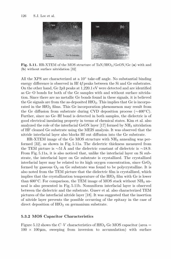
126 S.J. Lee et al.
(a) (b)
Fig. 5.11. HR-XTEM of the MOS structure of TaN/HfO2/GeON/Ge (a) with and(b) without surface nitridation [32]
All the XPS are characterized at a 10 take-off angle. No substantial bindingenergy difference is observed in Hf 4f peaks between the Si and Ge substrates.On the other hand, Ge 2p3 peaks at 1,220.1 eV were detected and are identifiedas Ge–O bonds for both of the Ge samples with and without surface nitrida-tion. Since there are no metallic Ge bonds found in these signals, it is believedthe Ge signals are from the as-deposited HfO2. This implies that Ge is incorpo-rated in the HfO2 films. This Ge incorporation phenomenon may result fromthe Ge diffusion from substrate during CVD deposition process (∼400C).Further, since no Ge–Hf bond is detected in both samples, the dielectric is ofgood electrical insulating property in terms of chemical states. Kim et al. alsoanalyzed the role of the interfacial GeON layer [17] formed by NH3 nitridationof HF cleaned Ge substrate using the MEIS analysis. It was observed that thenitride interfacial layer also blocks Hf out diffusion into the Ge substrate.
HR-XTEM image of the Ge MOS structure with NH3 annealing was per-formed [32], as shown in Fig. 5.11a. The dielectric thickness measured fromthe TEM picture is ∼51 A and the dielectric constant of dielectric is ∼18.9.From Fig. 5.11a, it is also noticed that, unlike the interfacial layer on Si sub-strate, the interfacial layer on Ge substrate is crystallized. The crystallizedinterfacial layer may be related to its high oxygen concentration, since GeO2
formed by gaseous O2 on Ge substrate was found to be polycrystalline. It isalso noted from the TEM picture that the dielectric film is crystallized, whichimplies that the crystallization temperature of the HfO2 film with Ge is lowerthan 600C. For comparison, the TEM image of MOS stack without NH3 an-neal is also presented in Fig. 5.11b. Nonuniform interfacial layer is observedbetween the dielectric and the substrate. Gusev et al. also characterized TEMpictures of the interfacial nitride layer [18]. It was suggested that the insertionof nitride layer prevents the possible occurring of the epitaxy in the case ofdirect deposition of HfO2 on germanium substrate.
5.3.2 MOS Capacitor Characteristics
Figure 5.12 shows the C–V characteristics of HfO2 Ge MOS capacitor (area =100 × 100 µm, sweeping from inversion to accumulation) with surface
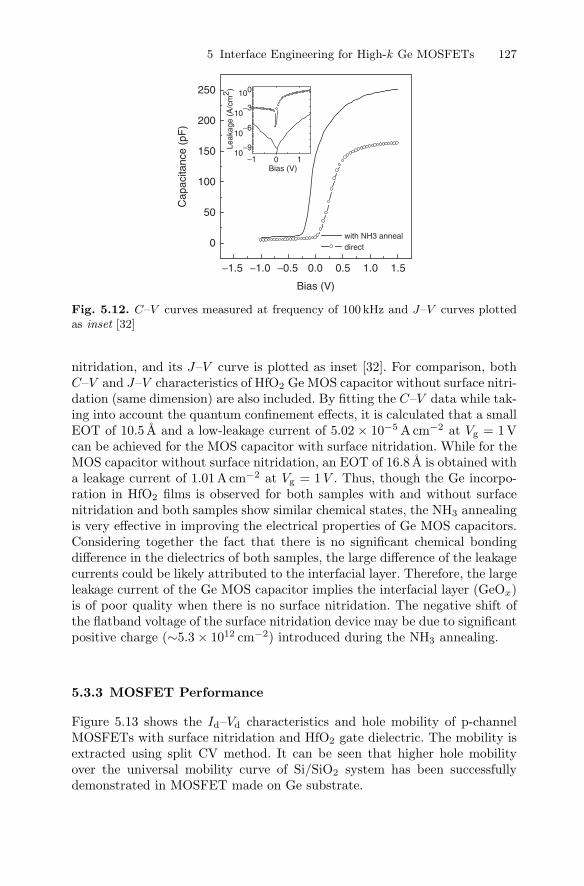
5 Interface Engineering for High-k Ge MOSFETs 127
−1.5 −1.0 −0.5 0.0 0.5 1.0 1.5
0
50
100
150
200
250
−1 0 110
−9
10−6
10−3
100
with NH3 annealdirect
Cap
acita
nce
(pF
)
Bias (V)
Lea
kage
(A
/cm
2 )
Bias (V)
Fig. 5.12. C–V curves measured at frequency of 100 kHz and J–V curves plottedas inset [32]
nitridation, and its J–V curve is plotted as inset [32]. For comparison, bothC–V and J–V characteristics of HfO2 Ge MOS capacitor without surface nitri-dation (same dimension) are also included. By fitting the C–V data while tak-ing into account the quantum confinement effects, it is calculated that a smallEOT of 10.5 A and a low-leakage current of 5.02 × 10⁻⁵ Acm−2 at Vg = 1Vcan be achieved for the MOS capacitor with surface nitridation. While for theMOS capacitor without surface nitridation, an EOT of 16.8 A is obtained witha leakage current of 1.01A cm−2 at Vg = 1V . Thus, though the Ge incorpo-ration in HfO2 films is observed for both samples with and without surfacenitridation and both samples show similar chemical states, the NH3 annealingis very effective in improving the electrical properties of Ge MOS capacitors.Considering together the fact that there is no significant chemical bondingdifference in the dielectrics of both samples, the large difference of the leakagecurrents could be likely attributed to the interfacial layer. Therefore, the largeleakage current of the Ge MOS capacitor implies the interfacial layer (GeOx)is of poor quality when there is no surface nitridation. The negative shift ofthe flatband voltage of the surface nitridation device may be due to significantpositive charge (∼5.3 × 1012 cm−2) introduced during the NH3 annealing.
5.3.3 MOSFET Performance
Figure 5.13 shows the Id–Vd characteristics and hole mobility of p-channelMOSFETs with surface nitridation and HfO2 gate dielectric. The mobility isextracted using split CV method. It can be seen that higher hole mobilityover the universal mobility curve of Si/SiO2 system has been successfullydemonstrated in MOSFET made on Ge substrate.

128 S.J. Lee et al.
−1.0 −0.8 −0.6 −0.4 −0.2 0.00
2
4Surface Nitridation
Id (
uA/u
m)
Vd (V)
|Vg-Vth|=0~0.9 Vstep=0.3 V
pFETL=20 um
0.1 0.2 0.3 0.4 0.5 0.6 0.70
40
80
120
160
200
240
Hol
eµ e
ff (c
m2 /v
-s)
Electric Field (MV/cm)
Surface Nitridation
Silicon Universal
Fig. 5.13. (a) Id–Vd characteristics and (b) hole mobility of p-MOSFET with HfO2
gate dielectric and surface nitridation [36]
Though a higher hole mobility of Ge over the Si counterparts has beensuccessfully demonstrated in MOSFETs with surface nitridation, a reasonablyhigh-electron mobility has not been demonstrated in n-channel MOSFETs onGe substrate using surface nitridation treatment. This is possibly because ofthe poor thermal stability of surface nitridation, which degrades the inter-face properties since a higher source/drain annealing temperature is neededto activate phosphorus than boron. Thus, a novel surface passivation withbetter thermal stability may be needed to provide well performed n-channelMOSFETs.
5.4 Surface Silicon Passivation
In Sect. 5.3, surface nitridation (SN) prior to high-k deposition on germa-nium substrate is proposed and investigated by introducing an interlayer ofultrathin nitride layer. However, the easier oxidation over nitridation of theGe substrate makes the nitride layer containing a high concentration of oxy-gen, which may degrade the blocking properties and causing poor interfaceproperties (thermal stability). Recently, a surface passivation using SiH4 an-nealing prior to high-k deposition has been proposed and investigated for theGe MOSFETs [36–38]. The silane surface passivation introduces an ultrathinlayer of Si which contributes to the interfacial layer during the subsequenthigh-thermal processing steps. This passivation is found to be able to pro-vide both high hole and electron mobility in p- and n-channel MOSFETs,respectively, due to the good interface properties.
5.4.1 Physical Characterization
An effective surface silicon passivation (SP) on germanium should meet thefollowing criteria (1) Si must completely cover the germanium surface andthe germanium surface should be free of germanium oxide and (2) the silicon

5 Interface Engineering for High-k Ge MOSFETs 129
1228 1224 1220 1216 12122
4
6
8
10
12
110 105 100 952.8
3.2
3.6
4.0
Ge-Ge
Inte
nsity
(c/
s)
Binding Energy
Ge-O
Ge 2p3
x104
(a) (b)
(a) after DHF cleaning(b) w/ SiH4 passivation
Inte
nsity
(c/
s)
Binding Energy (eV)
Si 2p
Si-Si
Si-O
(b)
x103
Fig. 5.14. The Ge 2p3 spectra of XPS on the passivation process on Ge surface bySiH4. The samples before and after passivation were compared. Inset shows the Si2p spectra of the sample after SiH4 passivation [37]
passivation layer should be thin enough and consumed during the subsequenthigh-k deposition so that the MOSFET channel is still kept in germanium.
Figure 5.14 shows the Ge 2p3 XPS spectra of the sample just after DHFcleaning and the sample after the SiH4 surface passivation. The inset is the Si2p XPS spectrum of the sample after the SiH4 surface passivation. As can beseen, the Ge–O peak observed on the DHF as-cleaned Ge surface disappearedafter the SiH4 passivation. Moreover, the Si-passivated Ge surface is stableeven the sample is exposed to the air. The existence of silicon is confirmed bythe Si 2p spectrum of the same sample, as shown in the inset. This Si signalincludes two types of bonds: one is the elemental Si, and the other is SiOx
(which is likely introduced during sample transportation). Based on the aboveanalysis, the germanium surface is completely covered by elemental Si and freeof germanium oxide after the SiH4 passivation. It is also noticed in Fig. 5.14that (1) the intensity of the Si–O peak (∼102.6 eV) is much lower (∼65 times)than that of the Ge–Ge peak (∼1217.4 eV) for the sample after passivationand (2) the Ge–Ge peak (∼1217.4 eV) of the sample after passivation shows anegligible intensity reduction compared to the as-cleaned sample. Both implythat the amount of the top silicon is so little that the thickness is muchless than the inelastic mean free path (IMFP) of Ge 2p3 electrons travelingin silicon. The small value of the IMFP (∼8.7 A) indicates the silicon layercould be only a few monolayers. AFM analysis was performed to examine thesurface roughness. It was found that comparable surface roughness betweenthe DHF-cleaned sample (RMS = 0.157 nm) and the Si-passivated sample(RMS = 0.166 nm) were observed.
The effect of the SiH4 surface passivation on the subsequent HfO2 de-position was studied by angle-resolved XPS analysis and shown in Fig. 5.15.The sample after HfO2 deposition without Si-passivation is included for com-parison. Both samples are characterized at take-off angles of 10 and 90,respectively. As can be seen, only the sample with Si passivation at the 90

130 S.J. Lee et al.
1227 1224 1221 1218 1215 1212
108 104 100 96
(d)
(c) (b)
(a)
(a) w/o SiH4 90o
(b) w/o SiH4 10o
(c) w/ SiH4 90o
(d) w/ SiH4 10o
Inte
nsity
(a.
u.)
Binding Energy (eV)
Ge-O
Ge-Ge
Ge 2p3
Binding Energy (eV)
Inte
nsity
(a.
u.) Si 2p
Si-O
(c)
Fig. 5.15. The Ge 2p3 spectra of angle-resolved XPS on the samples with andwithout passivation after HfO2 MOCVD [37]
take-off angle shows a two-peak spectrum [curve (c)], representing the ele-mental germanium and the germanium oxide states. The detection of elementGe bonds indicates that the HfO2 film on this sample is thinner than thesample without Si passivation [curve (a)]. Moreover, the Ge–O peak area ofthe Si passivated sample [curve (c)] is much smaller than that of the samplewithout passivation [curve (a)]. This means the passivation is very effectivein suppressing formation of germanium oxide. The small take-off angle (10)in the analysis was also used to examine the dielectric film. Obviously, theamount of Ge in the sample with Si passivation at 10 take-off angle is muchless than that of the sample without Si passivation. Thus, the significant Geout diffusion during HfO2 MOCVD is greatly suppressed by Si passivation.On the other hand, only Si at its oxide state is detected (the inset of Fig. 5.15),indicating that there is no Hf–silicide formation at the interface.
5.4.2 MOS Capacitors and Thermal Stability
Figure 5.16 shows a comparison between the two surface treatments. Thegate leakage currents of the p-MOS capacitors at |Vg − Vfb| = 1V underaccumulation were plotted as a function of the EOT. The theoretical gateleakage currents of SiO2/Si and HfO2/Si systems contributed by direct tun-neling mechanism are also plotted with solid lines. As is shown in Fig. 5.16,direct CVD HfO2 on germanium results in a large gate leakage current thatis higher than thermal SiO2 on Si at the same moderate EOTs. The forma-tion of unstable germanium oxide during the HfO2 CVD is the main cause ofthis large leakage. The large gate leakage current can be reduced by orders ofmagnitude by using either surface nitridation or Si passivation, as shown inFig. 5.16 with square and triangle dots. Although the two surface passivationtechniques both result in higher leakage currents than HfO2/Si system, it isnoticed that the gate leakage currents can still meet the requirements of bothhigh performance (HP) and low operation power (LOP) MOSFETs after the

5 Interface Engineering for High-k Ge MOSFETs 131
8 10 12 14 16 18 20 22 24 2610−9
10−7
10−5
10−3
10−1
101
103
HfO2/Si Surface Nitridation Silicon Passivation
2004
2004
2008
HfO2/Ge
(w/o surface treatment)
Jg (
A/c
m2 )
EOT (A)
SiO2/Si
2008
ITRS(HP) ITRS(LOP)
Fig. 5.16. Gate leakage current as a function of EOT of Ge MOS capacitors withdifferent surface passivation
year 2008 according to ITRS2003 (see Fig. 5.16). Further scaling of EOT canbe achieved by thinning down the high-k layer.
Since for n-MOS devices, a postmetal annealing temperature higher than500C is more favorable for activating the source/drain dopants and for repair-ing the source/drain implant damage, the thermal stability of the postmetalannealing (higher than 500C) on gate stack in terms of leakage current andEOT is analyzed with SP processed n-MOS capacitors (Fig. 5.17). The leakagecurrent is taken at −1 V gate bias. From the device without PMA to the deviceprocessed with the highest thermal budget (600C, 30 s), the leakage currentincreases by around one order of magnitude, and by a 2.8 A increase of EOT.Thus, a higher temperature PMA on the gate stack generally degrades the Ig-EOT characteristic. The increase of EOT might be due to additional growth
10−9
10−8
10−7
10−6
10−5
10−4
10
12
14
16
18
20
600c
30s
500c
10m
500c
5m
w/o P
MA
EO
T (
A)
Leak
age
Cur
rent
(A
/cm
2 )
Fig. 5.17. Dependences of EOT and gate leakage current on annealing condition

132 S.J. Lee et al.
−1.0 −0.5 0.0 0.5 1.00
2
4
6 Silicon PassivationSurface Nitridation
Id (
uA/u
m)
Vd (V)
L=20um|Vg-Vth|=0~0.9Vstep=0.3V
pFET
nFET
Fig. 5.18. Id–Vd characteristics of p- and n-FETs with silane surface passviationand surface nitridation [36]
of the interfacial layer. The increase of leakage current might be related to theGe out diffusion from the substrate into the oxide during the thermal anneal.
5.4.3 MOSFET Performance
To obtain high performance Ge p- and n-FETs with silicon passivation, twodifferent silicon passivation conditions (thin silicon and thick silicon) were em-ployed in the device fabrication. The starting Ge wafers (100) were subjectedto different surface treatments after DHF precleaning. The silicon passivation(SP) was carried out by annealing in SiH4. The ultrathin silicon layer willbe oxidized during the subsequent MOCVD HfO2 deposition and contributedto the interfacial layer. For comparison, both Ge devices with surface ni-tridation (conducted by annealing in NH3) and Si devices were fabricated.After HfO2 deposition and postdeposition anneal (PDA), PVD TaN was de-posited and patterned as metal gate. Boron and phosphorus were implantedand activated as source/drain. Finally, forming gas annealing was performedat 350C.
Charge pumping measurement was conducted and the interface trap densi-ties are 1.6×1012 cm−2 eV−1, 3.2×1011 cm−2 eV−1, and 4.5×1011 cm−2 eV−1
for SN Ge p-FET, SP Ge p-FET, and SP Ge n-FET, respectively. Figure 5.18shows the Id − Vd characteristics of the transistors. The SP p-FET shows a∼76% improved drain current over the SN p-FET under the same gate over-driver. Figure 5.19 shows the Id–Vg characteristics of the transistors. The Getransistors with SP technique exhibit larger on/off ratios than the transistorswith SN technique. A record-low subthreshold swing (72 mV dec−1) for p-FETis also achieved by SP technique. Split-CV measurement was used to extracteffective hole and electron mobility, respectively, for both n- and p-FETs.Figure 5.20 shows the effective hole and electron mobility of the transistors.The SP devices exhibit ∼82% higher hole mobility than the SiO2/Si universal

5 Interface Engineering for High-k Ge MOSFETs 133
−1.0 −0.5 0.0 0.5 1.0 1.5
10−1
100
10−2
10−3
10−4
Surface Nitridation Silicon Passivation
Id (
uA/u
m)
Vg (V)
L=20um|Vd|=0.05V
94mV/dec
72mV/dec
83mV/dec
Fig. 5.19. Id–Vg curves of p- and n-FETs with silane surface passivation and surfacenitridation [36]
curve at high field of 0.6 MVcm−1, and ∼61% higher peak electron mobilitythan the HfO2/Si device.
Further improvement in surface passivation may be needed to provide bet-ter mobility, particularly for the electron mobility. Bai et al. recently proposeda new surface passivation of using Si interlayer passivation and the subsequentnitridation of the Si interlayer [39]. An improved interface properties has beendemonstrated with this surface passivation technique.
5.4.4 BTI and Charge Trapping
BTI characteristics were measured in MOSFETs biased under inversion. Avoltage (Vstress) is applied to the gate of a device, while the source/drainand substrate are grounded. Measurements were conducted during the stressintervals. The measurement time between two consecutive stresses was ensuredto be minimal in order to reduce the possible detrapping of the oxide trappedcharge.
0.1 0.2 0.3 0.4 0.5 0.6 0.70
40
80
120
160
200
240
280
Hol
eµ e
ff(c
m2 /v
-s)
Electric Field (MV/cm)
Silicon Passivation
Surface Nitridation
Silicon Universal
0.1 0.2 0.3 0.4 0.5 0.6 0.70
40
80
120
160
200
240
HfO2/Ge (SP)
HfO2/Si controlEle
ctro
nµ e
ff(cm
2 /v-s
)
Electric Field (MV/cm)
Fig. 5.20. (a) effective hole mobility and (b) effective electron mobility as a functionof electrical field of p- and n-FETs made with silane surface passivation and surfacenitridation [36]

134 S.J. Lee et al.
101
102
103
−160
−120
−80
−40
0
Surface NitridationVth-1.1VVth-0.9VVth-0.7V
Silicon PassivationVth-1.4VVth-0.9VVth-0.7V
∆Vth
(m
V)
stress time (s)
pFET
EOT=13A
Fig. 5.21. NBTI degradation of Vth shift in p-FETs with silicon passivation andsurface nitridation [36]
Figure 5.21 shows the NBTI degradation of Vth shift with stressing for Gep-FETs as well as Si p-FETs. The Vth shift of the SP Ge p-FET is smallerthan the silicon control, which might be attributed to the larger valence bandoffset of HfO2/Ge and hence less hole trapping in the high-k dielectric than thesilicon counterpart. Thus, the SP Ge p-FET shows better NBTI characteristicsthan the silicon control. Figure 5.22 shows the PBTI degradation of Vth shiftwith stressing for Ge n-FETs with SP as well as Si n-FETs. The SP Ge n-FET shows a larger Vth shift than the silicon control, which suggests a severercharge trapping in the gate oxide. This may relate to the lower processingtemperature during the device fabrication, which results in a larger amountof preexisting electron traps in the dielectric. Thus, for high-k Ge MOSFETs,PBTI degradation is more significant than NBTI degradation.
Charge trapping characterization was conducted on Ge MOSFETsunder accumulation stress with a same stressing scheme as used in BTI
101
102
103
0
50
100
150
200
250
Silicon Passivation
Vth+0.9V
Vth+0.7V
Vth+0.5V
Si control
Vth+0.9V
∆Vth
(m
V)
stress time (s)
nFET
EOT=13A
Fig. 5.22. PBTI degradation of Vth in n-FETs with silicon passivation and surfacenitridation [36]

5 Interface Engineering for High-k Ge MOSFETs 135
101
102
103
0
50
100
150
200
250Surface Nitridation
Vfb+0.9VVfb+0.7VVfb+0.5V
Silicon PassivationVfb+0.9VVfb+0.7VVfb+0.5V∆V
th (m
V)
stress time (s)
pFET
EOT=13A
Fig. 5.23. Vth degradation of p-FETs due to charge trapping with silicon passivationand surface nitridation [36]
characterization. Figure 5.23 shows the Vth shift stressed at various voltagesfor all the p-FETs. SN Ge p-FET shows the highest Vth shift. The larger posi-tive Vth shift in SP Ge p-FET than Si control is due to more electron trappingin HfO2 on Ge substrate. This is consistent with the PBTI in n-FETs. Fig-ure 5.24 shows the Vth shift with stressing for both the Ge and Si n-FETs.It is noticed that the Vth shift in Ge n-FET is less than that in Si control.These also imply less hole trapping occurred in HfO2 on Ge substrate dueto the larger valence band offset (hole barrier) compared to the HfO2 on Sisubstrate.
5.5 Plasma-PH3 and AlN Surface Passivation
There have been noticeable efforts to study the reconstruction of semicon-ductor surfaces by removal of dangling bonds and surface states with proper
101
102
103
−25
−20
−15
−10
−5
0
Silicon PassivationVfb-1.6VVfb-1.4VVfb-1.2V
Si controlVfb-1.4V
∆Vth
(mV
)
stress time (s)
nFET
Accumlation stress
EOT=13A
Fig. 5.24. Vth degradation of n-FETs due to charge trapping with silicon passivationand surface nitridation [36]

136 S.J. Lee et al.
Fig. 5.25. XPS analysis of HfO2 on plasma-PH3 treated and thermal nitride Gesubstrate; (a) Ge 3d spectra after plasma-PH3 treatment, HfO2 deposition and PDA,(b) P 2p spectra on Ge after passivation by plasma-PH3 and HfO2 deposition, and(c) O 1s spectra on Ge after thermal nitridation and plasma-PH3 treatment withHfO2 [43]
surface treatments in order to restore the ideal bulk-terminated geometry onsemiconductor surfaces. On the Ge surfaces, several adsorbates have beeninvestigated to passivate the Ge surfaces; a monolayer of As by MBE [40],chemisorption of S by dissociation of Ag2S in UHV [41], adsorption of Cl andBr by dissociation of AgCl and AgBr [42].
Plasma-PH3 surface treatment was employed to passivate the Ge substrateprior to HfO2 deposition [43]. In this experiment, the HF-last n- and p-typeGe wafers received plasma treatment in PH3 ambient at 400C, followed byMOCVD HfO2 deposition and PDA at 500C, all the processes performed inin situ multicluster CVD system without breaking vacuum. Figure 5.25 showsthe XPS analysis of Ge, P, and O spectra for HfO2 on plasma-PH3 and thermalnitrided Ge substrate before and after PDA. First, the Ge 3d spectra indicatethat the Ge oxide is formed mainly during the CVD process with a littleincrease after PDA. The successful incorporation of P at the surface is detectedby the P–O peak in P 3p spectra. By comparing the O 1s spectra and itsdeconvolution for both plasma-PH3 treated and thermal nitrided samples, itwas found that Ge oxide formation at the surface is suppressed by plasma-PH3
passivation. Moreover, no significant out diffusion of Ge in HfO2 is confirmedby EDS and SIMS analysis. As a result, the improved C–V characteristicswithout interface state-related behavior were demonstrated by plasma-PH3
treated HfO2/Ge for both n- and p-MOS devices (Fig. 5.26). Thermal stabilitystudy at various postannealing temperatures also indicates that a plasma-PH3
treated HfO2/Ge stack maintains stable EOT and leakage current up to 600Canneal.
The predeposition of a layer that is thermodynamically more favorable toform oxide than Ge, prior to high-k deposition on Ge, can be expected to beeffective to suppress the Ge oxide formation at the interface. In fact, the ZrO2
formation in [20] was performed by the sputtering of Zr precursor films on

5 Interface Engineering for High-k Ge MOSFETs 137
2.5Plasma PH3
Plasma PH3
Sputtered AIN
Sputtered AIN
Thermal Nitridation
Thermal Nitridation
W/O surface passivation
(a)(b)
2.0
1.5
1.0
0.5
0.0−2 −1
C(µ
F/c
m2 )
2.5
2.0
1.5
1.0
0.5
0.0
C(µ
F/c
m2 )
0
Vg(V)1 2 −2 −1 0
Vg(V)1 2
Fig. 5.26. Measure high frequency C–V of (a) p-MOS and n-MOS capacitors ofTaN/HfO2/Ge stack with different Ge surface passivations [43]
the pretreated Ge surface, followed by oxidation with UV ozone technique,demonstrating free of any significant interfacial layer and EOT of ∼5 A. Thesputtered HfO2 films were deposited on Ge both by direct HfO2 depositionon Ge and by preformation of 1.5 nm Hf metal layer on Ge followed by HfO2
deposition [44]. Results showed that the thinner interfacial layer and thusthinner EOT were obtained from HfO2 deposited on Hf bottom layer. In [45],a thin AlN layer was deposited on HF-last Ge substrate prior to ALD-HfO2
deposition. XPS analysis showed that a thin AlN layer is oxidized during HfO2
and PDA, forming AlON layer, which is more effective to reduce the interfaciallayer than thermal nitrided passivation. Excellent C–V and thermal stabilityin terms of EOT and leakage current were also demonstrated.
5.6 Conclusion
A review of ongoing researches on high-k/Ge interface engineering ispresented. Recent results show that the high-k/Ge system revealed differentphenomena, compared to high-k/Si system, with regards to interfacial layerformation/control, high-k layer growth, and electrical properties. In order toprevent the degradation of electrical performances of high-k/Ge devices, sev-eral Ge passivation techniques prior to high-k deposition have been studiedusing nitridation, Si passivation, plasma-PH3 passivation, and AlN passiva-tion. Experimental results show that they are effective to suppress the for-mation of unstable Ge oxide and the diffusion of Ge into upper high-k layer,resulting in improved C–V and mobilities.
References
1. J. Bardeen and W.H. Brattain, Phys. Rev., p. 230 (1948)2. L.L. Chang and H.N. Yu, Proc. IEEE, Vol. 53, p. 316 (1965)

138 S.J. Lee et al.
3. K.L. Wang and P.V. Gray, TED, Vol. ED-22, p. 353 (1975)4. E.E. Crisman, et al., J. Elec. Soc., Vol. 129, 8, p. 1845 (1982)5. J.J. Rosenberg. et al., EDL, Vol. 9, 12, p. 639 (1988)6. S.C. Martin, et al., EDL, Vol. 10, 7, p. 325 (1989)7. T.N. Jackson, et al., EDL, Vol. 12, 11, p. 605 (1991)8. A.V. Rzhanov, et al., Thin Solid Films, Vol. 58, p. 37 (1979)9. K. Prabhakaran, et al., Surf. Sci., Vol. 325, p. 263 (1995)
10. N. Tabet, et al., Surf. Rev. Lett., Vol. 6, p. 1053 (1999)11. K. Prabhakaran, et al., Thin Solid Films, Vol. 369, p. 289 (2000)12. J. Oh, et al., J. Elect. Mat., Vol. 33, 4, p. 364 (2004)13. S.J. Lee, et al., JAP, Vol. 92, 5, p. 2807 (2002)14. G.D. Wilk, et al., JAP, Vol. 89, p. 5243 (2001)15. S.V. Elshocht, et al., APL, Vol. 85, 17, p. 3824 (2004)16. H. Kim, et al., APL, Vol. 83, 13, p. 2647 (2003)17. H. Kim, et al., APL, Vol. 85, 14, p. 2902 (2004)18. E.P. Gusev, et al., APL, Vol. 85, 12, p. 2334 (2004)19. A. Delabie, et al., JAP, Vol. 97, 064104 (2005)20. C.O. Chui, et al., EDL, Vol. 23, 8, p. 473 (2002)21. C.O. Chui, et al., IEDM 200222. C.O. Chui, et al., VLSI 200223. K. Kita, et al., APL, Vol. 85, 1, p. 52 (2004)24. V. Cracium, et al., APL, Vol. 75, p. 1261 (1999)25. Y. Kamata, et al., JJAP, Vol. 44, 4B, p. 2323 (2005)26. A. Dimoulas, et al., APL, Vol. 86, 223507 (2005)27. A. Dimoulas, et al., APL, Vol. 86, 032908 (2005)28. A. Dimoulas, et al., ME, Vol. 80, p. 34 (2005)29. S.J. Wang, et al., APL, Vol. 85, 19, p. 4418 (2004)30. V.V. Afanas’ev, et al., APL, Vol. 84, 13, p. 2319 (2004)31. W.P. Bai, et al., VLSI Symp. Tech. Dig., 2003, Vol. 121 (2003)32. N. Wu, et al., Appl. Phys. Lett., Vol. 84, 3741 (2004)33. H. Shang, et al., IEEE Electron Dev. Lett., Vol. 25, 135 (2004)34. C.O. Chui, et al., IEDM Tech. Dig., 2003, 18.3.1 (2003)35. C.O. Chui, et al., IEEE Electron Dev. Lett., Vol. 25, 274 (2004)36. N. Wu, et al., IEDM Tech. Dig., 2005, 22.5 (2005)37. N. Wu, et al., Appl. Phys. Lett., Vol. 85, 4127 (2004)38. N. Wu, et al., IEEE Electron Dev. Lett., Vol. 25, 631 (2004)39. W.P. Bai, et al., IEEE Electron Dev. Lett., Vol. 26, 378 (2005)40. R.D. Bringans, et al., Phys. Rev. Lett., Vol. 55, p. 533 (1985)41. T. Weser, et al., Phys. Rev. B, Vol. 35, p. 8184 (1987)42. R.D. Schnell, et al., Phys. Rev. B, Vol. 32, p. 8053 (1985)43. S.J. Whang, et al., IEDM 200444. K. Kita, et al., SSDM 2003, p. 292 (2003)45. F. Gao, et al., APL, Vol. 86, p. 1 (2005)

6
Effect of Surface Nitridation on the ElectricalCharacteristics of Germanium High-κ/MetalGate Metal-Oxide-Semiconductor Devices
D.Q. Kelly, J.J.-H. Chen, S. Guha, and S.K. Banerjee
Summary. We discuss the effect of surface nitridation on germanium high-κ/metalgate metal-oxide-semiconductor capacitors. Results from various groups concerningGe surface cleaning, surface annealing in ammonia, and the effect of nitridation onC–V and leakage current characteristics are presented and discussed. Electrical dataobtained by our group for devices incorporating alumina (Al2O3) and hafnia (HfO2)dielectrics is presented and explained. Capacitance–voltage and leakage current datafor capacitors with and without surface nitridation are compared, and the effectof various postdeposition anneals is given. It was found that surface nitridationimproves the electrical characteristics of both Al2O3 and HfO2 devices as evidencedby reduced C–V hysteresis and lower leakage. Flat band voltage shifts are presentedas a consequence of surface nitridation that can be remedied by postdepositionannealing.
6.1 Introduction
Germanium MOSFETs have attracted attention in recent years due to theirenhanced carrier transport and the advances that have been made in high-κgate dielectric technology [1–9]. Its higher bulk mobility for both electrons(2X) and holes (4X) relative to Si, as well as its demonstrated compatibilitywith high-κ dielectrics, makes Ge a potential candidate for improving MOS-FET channel mobility while allowing for continued aggressive scaling of thegate dielectric. Despite its demonstrated ability to improve drive current ca-pacity in MOSFETs, many engineering hurdles must still be overcome beforeGe can be integrated into future CMOS technology nodes.
Although a significant knowledge gap still remains in materials-related is-sues for Ge-based CMOS, Ge is not unfamiliar to the semiconductor industry,at least historically. The first transistors were made using Ge crystals. Silicontotally eclipsed Ge, however, due to the advantageous properties of its nativesilicon dioxide (SiO2). Unlike Si, Ge does not possess a stable natural oxidethat can passivate the surface, act as etch protection, or be used as a high-quality gate insulator [10, 11]. The thermodynamic instability of germanium

140 D.Q. Kelly et al.
dioxide (GeO2) was shown by Prabhakaran et al. [12], who reported thatlow-temperature annealing of GeO2 resulted in the transformation of GeO2
to GeO on the surface, which thermally desorbed at around 420C. Thermaldesorption at such low temperatures makes GeO2 impractical as a gate dielec-tric for CMOS processes that require high-temperature steps. Another majordrawback of GeO2 is that it is soluble in water [10–12], which rules out almostall wet chemical processes that would attempt to use the Ge native oxide asan etch barrier.
The native dielectrics of Ge, including GeO2, germanium nitride (Ge3N4)[13–15], and germanium oxynitride (GeOxNy) [13,16], have all been exploredas potential gate insulators for CMOS. In the 1990s, creative methods wereemployed for growing better-quality GeO2 on Ge for MOS applications [17,18].But since GeO2 is volatile at relatively low temperatures and is water-soluble,alternative fabrication schemes that cover one of the native dielectrics (orthe bare Ge surface) with a non-native insulator have proven more promis-ing. One of the earliest examples of the non-native dielectric approach wasreported in 1971 by Iwauchi and Tanaka, who demonstrated Ge MOSFETswith Al2O3 dielectrics using reactive DC sputtering of Al [19]. In 1986, Changet al. obtained good interface properties through the use of thick films of analuminium–phosphorus oxide mixture deposited over native GeO2 [20]. EvenSiO2 has been explored as a possible non-native insulator on Ge [21, 22], butwhile SiO2 has proven extremely successful on Si, its use on Ge has beenproven to be much less effective. The main reason for this is the poor qual-ity of the SiO2/Ge interface. A solution to the SiO2/Ge interface problemwas proposed by Vitkavage et al., who examined the possibility of deposit-ing a thin layer of Si onto the Ge substrate as a buffer layer prior to SiO2
deposition [21]. The Si interlayer seemed to improve the interface with theGe substrates, which was evidenced by a drastic reduction in the density ofinterface states [21].
The initial studies investigating non-native insulators on Ge concentratedon achieving good interface and bulk characteristics, and not necessarily onreducing the equivalent oxide thickness (EOT). As a result, most of the filmswere relatively thick, and would be unlikely to offer an EOT of less than 10 Ato advance beyond the sub-2 nm regime. For example, the 2005 ITRS roadmappredicts the EOT for high-performance logic to be 9 A by the year 2008 and5 A by 2012 [23]. Fortunately, the natural progression of these lines of researchhad led to the use of high-κ dielectrics, which do offer the potential of scalingbelow 10 A. The demonstrated compatibility of various high-κ materials withGe has ignited a flurry of interest in Ge-channel MOSFETs. The currentresearch is focused mainly on MOSFET feasibility for bulk Ge [1–6, 9], Ge-on-insulator (GOI) [8, 24], and strained Ge channels on Si [7, 25, 26], withparticular attention to understanding the Ge/high-κ interface and reducingthe EOT.
Much of the groundwork for high-κ/metal gate Ge-based MOSFETs hasalready been established. In 2002, Shang et al. reported a Ge p-MOSFET

6 Effect of Surface Nitridation on the Electrical Characteristics 141
with a thin GeOxNy and low-temperature oxide (LTO) gate stack on a bulkGe substrate, demonstrating 40% hole mobility enhancement over Si and anEOT of 80 A [5]. In the same year, Chui et al. reported mobility-enhancedGe p-MOSFETs with ultrathin (6–10 A) ZrO2 dielectrics fabricated by UVozone oxidation of sputtered Zr [3]. In the following year (2003), Bai et al.reported low-leakage MOS capacitors on Ge substrates with an EOT of 13 Aformed by rapid-thermal treatment of the Ge surface in NH3 followed by insitu rapid-thermal CVD of HfO2 [9]. Later that year, the same gate processwas used by Ritenour et al. to fabricate strained Ge-channel p-MOSFETs onSi substrates (using relaxed Si1−xGex buffer layers) with twice the low-fieldmobility of Si and an EOT of 16 A [7].
An important finding in the recent literature on Ge MOSFETs is the ef-fectiveness of using thin GeOxNy as a surface passivation layer for subsequenthigh-κ deposition [9, 27–31]. For example, the study by Bai et al. showedthat the formation of a GeOxNy passivation layer by rapid-thermal anneal-ing in NH3 prior to HfO2 deposition reduced the leakage current in MOScapacitors from 150 to 6mA cm−2 and lowered the EOT by a factor of 2 [9].Van Elshocht et al. attributed the improved electrical performance and lowerEOTs of nitrided devices to reduced updiffusion of Ge atoms into the HfO2
layer, prevention of HfO2 epitaxy, and significantly reduced interfacial layerthickness [27].
In this chapter, we will discuss results obtained by our group that examinethe effect of surface nitridation on the electrical characteristics of Ge MOS de-vices incorporating Al2O3 and HfO2 dielectrics. A detailed study of Ge wafercleaning conditions, dielectric deposition conditions, and anneal conditionswas performed, and their effect on the electrical properties of metal-gatedAl2O3/Ge and HfO2/Ge capacitors was evaluated. Given the high level ofinterest within the research community in this and related topics, we notethat a number of groups have published reports that complement our results.With this in mind, the specific results obtained by our group will be presentedin the larger context of results obtained by other groups. We will show thatsurface nitridation prior to Al2O3 or HfO2 deposition is important in reduc-ing hysteresis, interfacial layer formation, and leakage current. We will alsoobserve that surface nitridation introduces positive trapped charges and/ordipoles at the Ge/high-κ interface, resulting in significant flat band voltageshifts that can be mitigated by postdeposition anneals.
6.2 Germanium Surface Cleaning
Germanium surface preparation prior to high-κ deposition is vital for ob-taining high-quality, low-leakage gate stacks. Various methods have been pro-posed for removing the native oxide, eliminating surface contaminants, andproviding a passivation layer for the Ge surface [10,11,32–37]. Some cleaningand passivation methods are more suitable for MOS fabrication than others.

142 D.Q. Kelly et al.
A common yet less appropriate method for Ge surface cleaning is to use500–1,000 eV sputtered Ar+ ions followed by thermal annealing. Althoughion sputtering is effective in removing surface contaminants, it creates signif-icant ion-induced defects which cannot be removed completely by annealingalone [38]. Alternative methods involve wet chemical etching followed by theformation of a native oxide passivation layer. The passivating oxide is thenremoved in some cases by annealing under ultrahigh vacuum, leaving a surfacefree of contaminants [32–37]. If annealing in vacuum is not appropriate for aparticular MOS process, the native oxide is removed by other means, such asHF vapor etching [39].
For MOS devices it is clear that the cleaning of the Ge surface prior tosurface passivation and high-κ deposition is important for achieving high-quality interfaces with low interfacial layer thicknesses. The techniques thatinvolve wet chemical treatment followed by thermal annealing include thework of Prabhakarana et al. [32] and Akane et al. [33, 34]. Prabhakaranaet al. used a cyclical procedure of dipping the Ge substrate in a mixtureof H2O2 and H2O and removing the oxide by dipping in HF, followed bythe formation of a final native oxide passivation layer that was removed bythermal decomposition under ultrahigh vacuum annealing [32]. Using thisprocedure, the authors were unable to detect any C or O impurities with X-ray photoelectron spectroscopy (XPS) or Auger electron spectroscopy (AES).Akane et al. used an aqueous ammonia solution to remove the Ge nativeoxide, followed by a rinse in diluted H2SO4 and an H2O2 treatment to forma passive oxide layer [33]. Extremely smooth oxide surfaces were found usingatomic force microscopy (AFM). The passive oxide layer was again removedin ultrahigh vacuum by thermal annealing, and the surfaces were analyzedin situ using reflection high-energy electron diffraction (RHEED) to revealwell-ordered 2 × 1 diffraction patterns. A clean, smooth surface was inferredby subsequent high-quality crystal growth. The same group also showed theeffectiveness of cyclical H2O2 and HCl treatments followed by the formationof a protective oxide using NH4OH/H2O2/H2O and thermal desorption inultrahigh vacuum [34]. In this case, a clean surface was inferred by the lackof C contamination on the surface, as indicated by AES.
Zhang et al. tried UV ozonation of Ge to form a native GeO2 layer insteadof using wet chemical treatments [35]. Germanium wafers were degreased insuccessive rinses of trichloroethylene, acetone, and methanol followed by ul-trasonic rinsing in deionized (DI) water. The wafers were then exposed to UVin laboratory air for various times, which resulted in passive oxide layers withthicknesses on the order of a few nanometers. Annealing in ultrahigh vacuumwas then carried out, followed by characterization with XPS, AES, and elec-tron energy loss spectroscopy (EELS). For the samples that were cleaned withthe optimized UV exposure process, no C or O impurities were found withXPS or AES, and EELS spectra revealed no peaks corresponding to Ge–Obonds.

6 Effect of Surface Nitridation on the Electrical Characteristics 143
Cyclical treatments using HF and DI water have also been proposed asan effective cleaning technique. This process was introduced by Deegan etal. [36]. The process involved rinsing Ge samples in running purified DI waterfor approximately 20 s, dipping in 50% HF solution for 10 s, and rinsing again.This procedure was repeated a total of five times before drying the samplesin filtered N2 gas and immediately inserting them into a vacuum chamberfor thermal desorption of the native oxide and XPS analysis. The XPS datashowed a drastic reduction in Ge–O bonding. Due to the simplicity of thiscleaning technique, it has gained some popularity in the recent Ge MOSFETliterature.
The cleaning techniques described thus far have all involved a thermalannealing step in ultrahigh vacuum for native oxide removal. For some MOSprocesses that include high-κ deposition, an annealing step in ultrahigh vac-uum may not be desirable or even feasible. In fact, the native GeO2 in somecases may even be kept so it can be used as a starting layer for the formationof GeOxNy [29]. Instead of removing the native oxide in ultrahigh vacuum,Chui et al. used an HF vapor etch prior to ZrO2 deposition [39]. MOS ca-pacitor results were compared with samples that were treated in DI water fornative oxide removal as well as samples that retained the native oxide. Thedevices that underwent HF vapor treatments showed the highest electricalquality, as evidenced by having the lowest hysteresis and frequency dispersionin the capacitance–voltage characteristics. These devices also showed a shift ofonly 1.24 mV in the flat band voltage after 200 s of constant-current stressing,which indicates a good-quality gate stack.
The work performed by our group uses a recipe developed by Dr.Huiling Shang from the IBM T.J. Watson Research Center. The Ge waferswere prepared by solvent cleaning in successive rinses of hot isopropanol, ace-tone, and methanol (10 min each), followed by a 15-min DI water rinse toremove the native oxide. To eliminate surface contamination, Ge surface etch-ing was then performed using a cyclical rinse of H2O2 (30%), HCl/H2O (1 : 4),and DI water. The H2O2 oxidized the Ge surface and the HCl/H2O etchedaway the resulting GeO2. The HCl-based etch has been shown by Okumuraet al [34] to reduce the roughness of the Ge surface, as opposed to the use ofHF as the etchant. After repeating this etch three times, a protective layer ofGeO2 was formed by dipping the wafer in a solution of NH4OH/H2O2/H2O(0.5 : 1 : 10) prior to inserting the wafers into the load lock chamber ofan ultrahigh vacuum reactive atomic-beam deposition system. The systemis equipped with a boron nitride resistive heater that was used to heat thecleaned Ge wafers to 650C for 30 min to thermally desorb the native ox-ide layer. XPS studies showed that a 650C anneal in ultrahigh vacuum for30 min resulted in complete removal of the residual surface oxygen, as seenin Fig. 6.1. The O1s 531 eV core-level peak is no longer observable after the650C anneal. The inset in Fig. 6.1 also shows that the Ge surface is carbonfree [28].
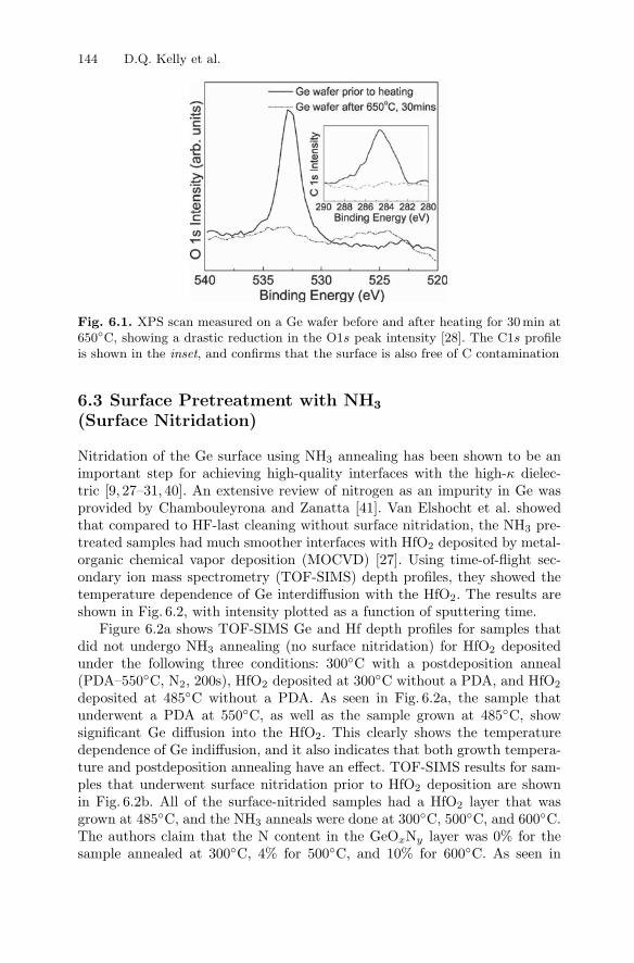
144 D.Q. Kelly et al.
Fig. 6.1. XPS scan measured on a Ge wafer before and after heating for 30 min at650C, showing a drastic reduction in the O1s peak intensity [28]. The C1s profileis shown in the inset, and confirms that the surface is also free of C contamination
6.3 Surface Pretreatment with NH3
(Surface Nitridation)
Nitridation of the Ge surface using NH3 annealing has been shown to be animportant step for achieving high-quality interfaces with the high-κ dielec-tric [9, 27–31, 40]. An extensive review of nitrogen as an impurity in Ge wasprovided by Chambouleyrona and Zanatta [41]. Van Elshocht et al. showedthat compared to HF-last cleaning without surface nitridation, the NH3 pre-treated samples had much smoother interfaces with HfO2 deposited by metal-organic chemical vapor deposition (MOCVD) [27]. Using time-of-flight sec-ondary ion mass spectrometry (TOF-SIMS) depth profiles, they showed thetemperature dependence of Ge interdiffusion with the HfO2. The results areshown in Fig. 6.2, with intensity plotted as a function of sputtering time.
Figure 6.2a shows TOF-SIMS Ge and Hf depth profiles for samples thatdid not undergo NH3 annealing (no surface nitridation) for HfO2 depositedunder the following three conditions: 300C with a postdeposition anneal(PDA–550C, N2, 200s), HfO2 deposited at 300C without a PDA, and HfO2
deposited at 485C without a PDA. As seen in Fig. 6.2a, the sample thatunderwent a PDA at 550C, as well as the sample grown at 485C, showsignificant Ge diffusion into the HfO2. This clearly shows the temperaturedependence of Ge indiffusion, and it also indicates that both growth tempera-ture and postdeposition annealing have an effect. TOF-SIMS results for sam-ples that underwent surface nitridation prior to HfO2 deposition are shownin Fig. 6.2b. All of the surface-nitrided samples had a HfO2 layer that wasgrown at 485C, and the NH3 anneals were done at 300C, 500C, and 600C.The authors claim that the N content in the GeOxNy layer was 0% for thesample annealed at 300C, 4% for 500C, and 10% for 600C. As seen in

6 Effect of Surface Nitridation on the Electrical Characteristics 145
Time500 1000
102
103
104
100
101
102
103
104
Inte
nsity
(a.
u.)
300°C
500°C
600°C
Ge
Hf
Time500 1000
Inte
nsity
(a.
u.)
Hf
Ge300°C+PDA
300°C485°C
Ge
(a)
(b)
Fig. 6.2. TOF-SIMS profiles of Hf and Ge atoms for HfO2 layers grown onGe by MOCVD [27]. (a) Depth profiles for HfO2 grown on Ge at 300C(with and without PDA) and 485C with no subsequent NH3 annealing. (b)Depth profiles for HfO2 grown on Ge at 485C after annealing in NH3 at300C, 500C, and 600C. Reused with permission from Van Elshocht et al. Ap-plied Physics Letters, 85, 3824 (2004). Copyright 2004, American Institute ofPhysics

146 D.Q. Kelly et al.
Fig. 6.2b, the 300C NH3 anneal did not prevent Ge diffusion into the HfO2
at all. The samples annealed at 500C and 600C, however, show suppressedGe diffusion. Since the TOF-SIMS data for the 500C and 600C anneals inFig. 6.2b look the same, the authors claim that a minimum amount of N is re-quired to prevent Ge diffusion, which they observed to saturate at around 4%.The authors conclude that the prevention of Ge diffusion into the HfO2 mightbe the reason for the improved electrical characteristics for surface-nitridedGe/high-κ MOS devices reported in the literature [27]. They also point outthat while samples without nitridation (Fig. 6.2a) have lower Ge diffusion,the high-κ oxides are more prone to crystallization, which causes much higherleakage.
It should be noted here that Seo et al. observed interfacial layer formationprior to molecular beam deposition of HfO2 caused increased traces of Geatoms to be detected in the oxide [42]. This result contradicts the resultsdescribed earlier, but they attributed it to higher instability of the interfaciallayers grown with an atomic O or N beam. In this case, the Ge atoms originatefrom the interfacial layers rather than the substrate. They also used lowergrowth temperatures (225C) where diffusion from the substrate is limited.
Van Elshocht et al. also examined the effect of surface nitridation on filmquality with cross-sectional transmission electron microscopy (XTEM) [27].Figure 6.3 shows images for HfO2 deposited on Si, Ge, and Ge with NH3
annealing. From the XTEM images we see that the HfO2 films that weregrown directly on Ge without surface nitridation showed much higher interfaceroughness compared to surface-nitrided devices (compare Fig. 6.3b, c). In ad-dition, comparisons of XTEM images with HfO2 grown on Si wafers (Fig. 6.3a)revealed that the interfacial layer is much thinner on Ge. The authors concludethat both Ge diffusion and crystallization increase the interface (and/or sur-face) roughness, and that these can be mitigated using surface nitridation.
Lu et al. studied Ge diffusion and its impact on the electrical propertiesof HfO2/Ge capacitors with TaN gates [30]. Figure 6.4 shows SIMS resultsfor three Ge samples that underwent different surface preparation techniques.The ion intensity ratio of Ge to Hf is plotted as a function of sputtering depthfor samples with Ge native oxide (no surface preparation), HF-last cleaning,and surface nitridation. It is immediately apparent that the surface-nitridedsample shows reduced Ge diffusion into the HfO2 layer. This is consistentwith the results of Van Elshocht et al. [27]. The authors of [30] proposedtwo mechanisms that could lead to Ge diffusion into the high-κ dielectric,both of which are related to the existence and amount of GeO2. The firstproposed mechanism was the following reaction taking place at the interface:Ge + GeO2 → 2GeO. The resulting volatile GeO (see also Kamata et al. [43])was thought to diffuse through the oxide and into the high-κ dielectric duringgrowth and postdeposition annealing, with the rate of diffusion enhanced byimpurities in the HfO2. The other proposed mechanism was the desorptionof Ge-enriched volatile Hf–Ge–O formed at the HfO2/GeO2 interface. One Hfatom would replace a Ge atom from the oxide since Hf is more electropositive

6 Effect of Surface Nitridation on the Electrical Characteristics 147
Fig. 6.3. XTEM images of HfO2 deposited on (a) Si, (b) Ge, and (c) Ge with NH3
annealing for surface nitridation [27]. The surface-nitrided sample shows a muchsmoother interface, and both Ge samples have reduced interfacial layer thicknesses.Reused with permission from Van Elshocht et al. Applied Physics Letters, 85, 3824(2004). Copyright 2004, American Institute of Physics
[44]. Since surface nitridation consumes all of the GeO2, both of the proposedmechanisms for Ge diffusion are suppressed.
6.4 Effect of Surface Nitridation on the ElectricalCharacteristics of Germanium MOS Capacitors
Several groups have observed the positive effect of surface nitridation on theelectrical characteristics of Ge MOS capacitors [9,27–31,40]. The consensus inthe research literature is that nitridation (typically achieved through NH3 an-nealing) decreases leakage current and improves the C–V characteristics. Gu-sev et al. compared C–V and leakage characteristics for HfO2/Ge capacitorswith Ge surface nitridation at with different NH3 annealing temperatures [40].Figure 6.5 shows C–V characteristics and leakage current data (inset) for Gesamples annealed in NH3 for 1 min at 550C, 600C, and 650C. As seen in

148 D.Q. Kelly et al.
Fig. 6.4. SIMS profiles showing the ratio of Ge and Hf ion intensities in Ge sampleswith native GeO2 (no surface preparation), HF-last surface preparation, and surfacenitridation [30]. The surface-nitrided sample shows significantly reduced diffusion ofGe atoms into the HfO2. Reused with permission from Lu et al. Applied PhysicsLetters, 87, 051922 (2005). Copyright 2005, American Institute of Physics
Fig. 6.5, the EOT decreases with increasing annealing temperature. Althoughnot shown in [40], the C–V characteristics for samples that did not undergoNH3 annealing were said to resemble the characteristics for MIM structures,which was attributed to the formation of Hf–germanide bonds at the interface.
Al on n-GeArea = 10−4cm2
160
140
120
100
80
60
40
20
50 A HfO2,
as deposited
c
b
a
10−1
10−2
10−3
10−4
10−5
10−6
10−70
0
1
1−1
2
2
3
3
Vg, V
c
ba
Jg, A/cm2
Gate bias (V)
Tqm ~ 1.6 nm
Tqm ~ 2.2 nm
Tqm ~ 1.9 nm
Cap
acit
ance
(p
F)
Fig. 6.5. Capacitance–voltage and leakage (inset) characteristics of HfO2/Ge ca-pacitors fabricated on Ge samples annealed in NH3 for 1min at (a) 550C, (b)600C, and (c) 650C. Reused with permission from Gusev et al. Applied PhysicsLetters, 85, 2334 (2004). Copyright 2004, American Institute of Physics
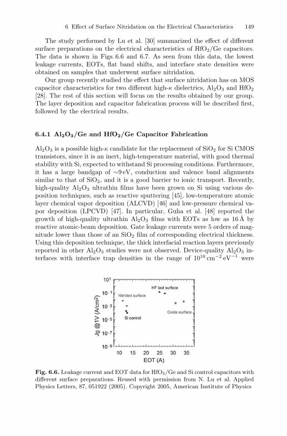
6 Effect of Surface Nitridation on the Electrical Characteristics 149
The study performed by Lu et al. [30] summarized the effect of differentsurface preparations on the electrical characteristics of HfO2/Ge capacitors.The data is shown in Figs. 6.6 and 6.7. As seen from this data, the lowestleakage currents, EOTs, flat band shifts, and interface state densities wereobtained on samples that underwent surface nitridation.
Our group recently studied the effect that surface nitridation has on MOScapacitor characteristics for two different high-κ dielectrics, Al2O3 and HfO2
[28]. The rest of this section will focus on the results obtained by our group.The layer deposition and capacitor fabrication process will be described first,followed by the electrical results.
6.4.1 Al2O3/Ge and HfO2/Ge Capacitor Fabrication
Al2O3 is a possible high-κ candidate for the replacement of SiO2 for Si CMOStransistors, since it is an inert, high-temperature material, with good thermalstability with Si, expected to withstand Si processing conditions. Furthermore,it has a large bandgap of ∼9 eV, conduction and valence band alignmentssimilar to that of SiO2, and it is a good barrier to ionic transport. Recently,high-quality Al2O3 ultrathin films have been grown on Si using various de-position techniques, such as reactive sputtering [45], low-temperature atomiclayer chemical vapor deposition (ALCVD) [46] and low-pressure chemical va-por deposition (LPCVD) [47]. In particular, Guha et al. [48] reported thegrowth of high-quality ultrathin Al2O3 films with EOTs as low as 16 A byreactive atomic-beam deposition. Gate leakage currents were 5 orders of mag-nitude lower than those of an SiO2 film of corresponding electrical thickness.Using this deposition technique, the thick interfacial reaction layers previouslyreported in other Al2O3 studies were not observed. Device-quality Al2O3 in-terfaces with interface trap densities in the range of 1010 cm−2 eV−1 were
Fig. 6.6. Leakage current and EOT data for HfO2/Ge and Si control capacitors withdifferent surface preparations. Reused with permission from N. Lu et al. AppliedPhysics Letters, 87, 051922 (2005). Copyright 2005, American Institute of Physics

150 D.Q. Kelly et al.
3
2.5
1013
1012
1011
1010
109
Del
ta V
fb (
V)
Dit
(cm
−2/e
V)
Oxide HF last NitridedSurface Conditions
2
1.5
0.5
0
1
Fig. 6.7. Flat band voltage shifts and interface state densities for HfO2/Ge capac-itors with different surface preparations. Reused with permission from N. Lu et al.Applied Physics Letters, 87, 051922 (2005). Copyright 2005, American Institute ofPhysics
obtained. We made use of the same reactive atomic-beam deposition tech-nique to deposit ultrathin Al2O3 films on bulk Ge.
Following the oxide desorption described earlier, Al2O3 was deposited onthe Ge wafers in situ using an atomic-beam deposition system. The systemconsisted of a modified molecular beam epitaxy (MBE) chamber equippedwith two radio frequency (RF) discharge sources, used to excite either O2
or N2 molecules to produce beams of atomic oxygen or nitrogen directed atthe sample surface. Al2O3 was grown at temperatures between 250C and300C through simultaneous exposure of Al from a resistively heated high-temperature effusion source and reactive atomic oxygen from the RF dischargesource [49]. The Al2O3 films were deposited on either as-cleaned or surface-nitrided Ge substrates. Surface nitridation of the Ge took place between 350Cand 600C by exposure to an atomic nitrogen beam from an RF source at350 W for 30 s. The N2 flow rate is maintained at 3 sccm. The Al2O3 filmswere then treated to various postdeposition anneals (under forming gas orO2) before Al electrodes were evaporated through a shadow mask to definecapacitors with areas ranging from 10−5 to 10−3 cm2.
HfO2 has received considerable attention as the leading high-κ dielec-tric candidate for sub-100 nm technology due to its high dielectric constant(∼21–25), reasonably large bandgap (6 eV), and superior thermal stabilitywith conventional polysilicon gates [50]. Kang et al. report that even after ahigh-temperature anneal treatment at 1,000C, no detectable interfacial layerformation occurred between the HfO2 and polysilicon [51]. The thermal sta-bility of HfO2 separates it from other high-κ candidates that have similardielectric constants and bandgaps but lower thermal stability, such as ZrO2.(In fact, ZrO2 has been shown to react with polysilicon to form silicides attemperatures above 900C, which degrades the electrical properties [52, 53].It is also unclear whether the HfO2/Ge and ZrO2/Ge systems show the same

6 Effect of Surface Nitridation on the Electrical Characteristics 151
thermal stability characteristics.) Furthermore, it has been shown that it ispossible to deposit ultrathin HfO2 films (EOT ∼ 10 A) on Si that have leakagecurrent levels more than 4 orders of magnitude lower than that of an SiO2
film with equivalent thickness [54].Using the same reactive atomic-beam deposition technique that we used to
deposit Al2O3, we have deposited ultrathin HfO2 films on Ge. Similar to ourwork, Dimoulas et al. have examined HfO2 deposited using an atomic-beamtechnique, but focused instead on frequency dispersion effects in much lowerEOT gate stacks and Pt gates [55]. For our work, two different gate metals, Aland W, were evaluated for the gate electrode. The surface preparation stepsfor these wafers prior to HfO2 deposition were identical to those applied tothe Ge wafers with Al2O3 deposition. Following oxide desorption, as was thecase with the Al2O3 samples, surface nitridation of the Ge was performed attemperatures between 350C and 600C by exposure to an atomic N beamfrom a RF discharge source, at 350 W for 30 s. For HfO2 growth, the Gesubstrate was heated to temperatures between 50C and 300C and exposedsimultaneously to Hf from an electron-beam evaporation source and reactiveatomic oxygen from the RF discharge source. The growth temperature waskept low to minimize interaction between Ge and Hf.
After HfO2 deposition, the Ge wafer was drawn back into the load lock ofthe system and subjected to UV ozone oxidation to further improve the stoi-chiometry of the film. Room-temperature UV ozone oxidation has been shownto be successful in producing good-quality oxide films, without significantlyincreasing the interfacial layer thickness [56]. The load lock is equipped with aHg vapor lamp, operated at about 50mW cm−2, which emits UV radiation atwavelengths of 185 and 254 nm. In the presence of the UV radiation, the loadlock is flooded with O2 gas at a pressure of 600 Torr for 60 min. The energiescorresponding to these particular wavelengths of UV light are very close tothe bond energies of O2 (∼5 eV) and O3 (∼1.1 eV) [57] and interact with theoxygen gas to produce oxygen radicals and ozone, both of which react withthe deposited HfO2 film. MOS capacitors were fabricated using either Al or Wmetal. HfO2 capacitors with Al gates were treated to postdeposition annealsbefore Al metal evaporation, which was performed through a shadow mask inthe same manner as the Al2O3 capacitors. The capacitors with W gates wereformed by in situ e-beam evaporation of blanket W films after the deposition ofthe HfO2, followed by standard photolithography and wet etch for defining thecapacitor electrodes. Subsequent postdeposition anneals were then carried out.
The deposition of HfO2 directly on Ge, without surface nitridation, re-sulted in the formation of an interfacial GeOx layer, although this resultcannot be generalized (Fig. 6.3b). This was verified by medium-energy ionscattering (MEIS) analysis on as-deposited HfO2/Ge samples, and the depthprofiles are shown in Fig. 6.8 [28]. Figure 6.8a shows that for the non-surfacenitrided sample, the O depth profile extends well beyond that of the Hf. Thisindicates the presence of an interfacial oxide. A quantitative modeling of theMEIS spectrum gave 6 A of interfacial GeO2 and 33 A of HfO2. HfO2 deposited

152 D.Q. Kelly et al.
Fig. 6.8. MEIS depth profiles of Hf and O distributions for HfO2 films deposited onGe. (a) HfO2 deposited on non-nitrided Ge [28]. The O atoms extend deeper thanthe Hf, due to an interfacial GeO2 layer. (b) Hf and O depth distributions for HfO2
deposited on nitrided Ge. The interfacial GeO2 layer is still present, but its extentis reduced compared to (a)
on a surface-nitrided Ge was also analyzed with MEIS (Fig. 6.8b), and it wasshown that the O atoms did not extend as far beyond the Hf. The surface-nitrided sample was modeled to have a thinner interfacial GeO2 layer of 4 A.
6.4.2 Electrical Characterization of Al/Al2O3/Ge Capacitors
High-frequency C–V measurements were carried out on the Al/Al2O3/Gecapacitors from 10 kHz to 1 MHz using an HP4284A LCR meter. Figure 6.9
Fig. 6.9. Comparison of C–V characteristics for Al/Al2O3/Ge capacitors with andwithout surface nitridation [28]. The surface-nitrided samples had significant reduc-tion in hysteresis, but also exhibited a large shift in the flat band voltage

6 Effect of Surface Nitridation on the Electrical Characteristics 153
Fig. 6.10. Comparison of C–V characteristics for Al/Al2O3/Ge surface-nitridedcapacitors with and without a PDA in O2 for 30 min at 550C [28]. The surface-nitrided samples had significant reduction in hysteresis [14], but also exhibited alarge shift in the flat band voltage
shows high-frequency (1 MHz) C–V measurements taken for two Al/Al2O3/Gecapacitors, with and without surface nitridation. The surface nitridation, car-ried out at 350C, significantly reduced hysteresis from 500 mV to 20 mV,implying a reduction in charge trapping at the interface. Surface nitridationalso reduced the interface state density (Dit) from 2 × 10¹² eV−1 cm−2 to4 × 1011 eV−1 cm−2, which indicates a higher quality interface. As seen inFig. 6.9, however, the flat band voltage (VFB) exhibits a large negative shiftfor the surface-nitrided samples. The ∆VFB is approximately −0.8V. Theexplanation could be that positive charge was somehow introduced at theinterface during the nitridation process. It might also be possible that a di-electric polarization layer formed as a result of the nitridation. The VFB shiftcan be partially corrected, however, by performing a PDA in O2 ambient.Figure 6.10 compares high-frequency C–V characteristics for a Al/Al2O3/Gecapacitor that underwent a PDA in O2 for 30 min at 550C to a device that didnot undergo an O2 anneal. We notice immediately that the ∆VFB is reversed,pushing the flat band voltage toward its ideal position.
The EOT of the non-nitrided sample dielectric was 24 A, while the EOTfor nitrided gate stack was reduced to 22 A. Both Al2O3 films were depositedunder identical growth conditions except for the starting Ge surface. Thisreduction in equivalent film thickness is due to the presence of the thin ni-tride layer on the nitrogen-passivated Ge surface, which provides a sufficientbarrier to interfacial reaction during dielectric deposition. Similar reductionhas been also observed for other high-κ dielectrics deposited on Si [15] andGe [9] substrates.
Surface nitridation was also observed to reduce the leakage current den-sity, as shown in Fig. 6.11. The leakage current density for the non-nitridedAl/Al2O3/Ge capacitor at 1 V is 7×10⁻³ Acm−2. In order to make a meaning-ful comparison between the leakage current densities between the capacitors

154 D.Q. Kelly et al.
Fig. 6.11. Comparison of leakage current density characteristics for Al/Al2O3/Gecapacitors with and without surface nitridation [28]. Surface nitridation reduces theleakage current by nearly three orders of magnitude at equivalent V −VFB, denotedby the dashed lines
with and without surface nitridation, we have to take into account the differ-ence in the VFB. (Many reports in the literature show leakage currents at ap-plied biases of ±1V , but sometimes this can be misleading. It is always impor-tant to take into account the differences in VFB for measuring leakage currents,since bulk and interface charges can compensate the applied bias.) Since thenitrided sample exhibited a ∆VFB of −0.8V, we should compare the leakagecurrent measured at a bias of 0.2 V. The corresponding leakage current den-sity for the Al/Al2O3/Ge sample with surface nitridation (at 0.2 V) was about1×10−5 Acm−2, representing a reduction of nearly three orders of magnitude.
The O2 anneal at 550C for 30 min, in addition to recovering the ∆VFB,also improved the leakage current. The EOT increased after the O2 anneal(Fig. 6.10), which explains the lower leakage. Figure 6.12 shows the effect oftwo types of PDA on the leakage current density characteristics of nitridedAl/Al2O3/Ge capacitors. The O2 anneal improves the leakage current densityby an order of magnitude compared to the as-deposited stack. The currentdensity measured at 1 V is 2 × 10⁻⁶ Acm−2. This leakage current is threeorders of magnitude lower than SiO2 with equivalent thickness [58]. An annealin forming gas at 550C for 30 min, by comparison, makes the leakage currentworse than the as-deposited case.
Charge trapping measurements were carried out on the Al/Al2O3/Ge de-vices using a square pulse technique described in [59]. This technique allows forthe measurement of both the trapped charge density (Nox) and the trappingprobability (Pn). We define trapping probability as Pn = q∆Nox/∆Qinj, where∆Nox is the change in the trapped charge density and ∆Qinj is the change inthe injected charge. The charge trapping measurements done under substrateinjection conditions at a stress bias of 1 V. Figure 6.13a shows the Nox as afunction of injected charge for the Al2O3 capacitor stack on non-nitrided andsurface-nitrided Ge, including the case where the nitrided sample underwent a
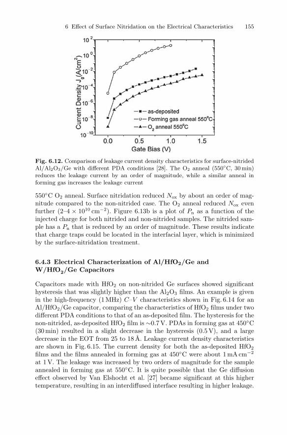
6 Effect of Surface Nitridation on the Electrical Characteristics 155
Fig. 6.12. Comparison of leakage current density characteristics for surface-nitridedAl/Al2O3/Ge with different PDA conditions [28]. The O2 anneal (550C, 30 min)reduces the leakage current by an order of magnitude, while a similar anneal informing gas increases the leakage current
550C O2 anneal. Surface nitridation reduced Nox by about an order of mag-nitude compared to the non-nitrided case. The O2 anneal reduced Nox evenfurther (2–4 × 1010 cm−2). Figure 6.13b is a plot of Pn as a function of theinjected charge for both nitrided and non-nitrided samples. The nitrided sam-ple has a Pn that is reduced by an order of magnitude. These results indicatethat charge traps could be located in the interfacial layer, which is minimizedby the surface-nitridation treatment.
6.4.3 Electrical Characterization of Al/HfO2/Ge andW/HfO2/Ge Capacitors
Capacitors made with HfO2 on non-nitrided Ge surfaces showed significanthysteresis that was slightly higher than the Al2O3 films. An example is givenin the high-frequency (1 MHz) C–V characteristics shown in Fig. 6.14 for anAl/HfO2/Ge capacitor, comparing the characteristics of HfO2 films under twodifferent PDA conditions to that of an as-deposited film. The hysteresis for thenon-nitrided, as-deposited HfO2 film is ∼0.7V. PDAs in forming gas at 450C(30 min) resulted in a slight decrease in the hysteresis (0.5 V), and a largedecrease in the EOT from 25 to 18 A. Leakage current density characteristicsare shown in Fig. 6.15. The current density for both the as-deposited HfO2
films and the films annealed in forming gas at 450C were about 1mA cm−2
at 1 V. The leakage was increased by two orders of magnitude for the sampleannealed in forming gas at 550C. It is quite possible that the Ge diffusioneffect observed by Van Elshocht et al. [27] became significant at this highertemperature, resulting in an interdiffused interface resulting in higher leakage.

156 D.Q. Kelly et al.
Fig. 6.13. (a) Trapped charge density (Nox) as a function of injected charge (Qinj)for Al/Al2O3/Ge capacitors [28]. Nox is reduced by surface nitridation, and is re-duced further by a 550C, 30-min O2 anneal. (b) Effect of surface nitridation ontrapping probability (Pn)
Surface nitridation of the Al/HfO2/Ge capacitors (prior to HfO2 deposi-tion) was carried out at 500C. The effect on the C–V characteristics canbe seen in Fig. 6.16. Figure 6.16 shows C–V characteristics for Al/HfO2/Gecapacitors with and without surface nitridation, with either 450C or 550Cforming gas PDAs. For the 450C forming gas PDA, we observe a reductionin the EOT from 18 to 14 A. The nitridation again introduced a negative
Fig. 6.14. C–V characteristics for non-nitrided Al/HfO2/Ge capacitors under dif-ferent PDA conditions [28]. The forming gas anneal at 450C slightly reduced thehysteresis and decreased the EOT. The 550C severely degraded the C–V charac-teristics

6 Effect of Surface Nitridation on the Electrical Characteristics 157
Fig. 6.15. Leakage characteristics for Al/HfO2/Ge capacitors under different PDAconditions [28]. The as-deposited HfO2 film and the film annealed at 450C in form-ing gas had similar gate leakage, but the sample annealed at 550C had two ordersor magnitude higher leakage
∆VFB of −0.7V (from −0.5V). The hysteresis on the 450C PDA sample wasreduced from 500 to 80 mV with nitridation. These results are similar to thetrends observed in our surface-nitrided Al/Al2O3/Ge capacitors. Observingthe C–V characteristic for the sample annealed at 550C, we see that thenitridation process afforded an increase in the PDA temperature. This is ad-vantageous because at the higher temperature of 550C, we observe a reversalof the ∆VFB back toward 0 V, indicating charge compensation or reduction.The C–V hysteresis was reduced to only 10 mV.
Figure 6.17 shows leakage current curves for nitrided and non-nitridedAl/HfO2/Ge capacitors with 450C or 550C forming gas anneals. The ni-trided capacitors exhibited two orders of magnitude lower leakage than the
Fig. 6.16. C–V characteristics for Al/HfO2/Ge capacitors under two different form-ing gas PDA conditions, with and without surface nitridation [28]. Surface nitrida-tion improved hysteresis and reduced the EOT

158 D.Q. Kelly et al.
Fig. 6.17. Leakage characteristics for Al/HfO2/Ge capacitors under two differentforming gas PDA conditions, with and without surface nitridation [28]. Surfacenitridation reduced the leakage current by two orders of magnitude
non-nitrided samples. Although the forming gas PDA at 550C is raised byslightly more than an order of magnitude over the sample with a 450C PDA,the leakage current remained low. The current density was 1 × 10⁻⁵ Acm−2
at (VFB + 1V), which is six orders of magnitude less than SiO2 of the sameequivalent thickness of 14 A [58].
The surface-nitrided Al/HfO2/Ge capacitor, after undergoing forming gasPDA at 550C, gave the most promising results (EOT ∼ 14 A, hysteresis∼10mV, and low leakage current density of 1 × 10⁻⁵ Acm−2) but someissues remain that need to be addressed. These capacitors still exhibit somefrequency dispersion behavior in the C–V depletion region due to a largeconcentration of interface states. Using the combined high–low frequencycapacitance method, the interface state density, Dit, was calculated to bearound 8 × 10¹² eV−1 cm−2 near the midgap.
A few conclusions may be drawn regarding the role of surface nitridationfor both the Al2O3 and the HfO2 films. Nitrided films are consistently thinnerthan non-nitrided ones, suggesting reduced interfacial GeO formation. This isconsistent with what is observed in the case of nitridation of Si surfaces priorto SiO2 gate dielectric formation. Nitridation also substantially reduces thehysteresis observed in the C–V plots. The reason for this is not clear, thoughit may be tied to the reduction in GeO formation. We also see that surfacenitridation produces a negative shift in VFB that can be partially recoveredby annealing. Finally, the thin nitride layer at the interface reduces leakagecurrent across the film.
The results shown so far have been for Al electrodes on the HfO2. However,Al electrodes are known to form an Al2O3-containing interface layer [59]. Thisinterfacial layer inevitably increases the EOT. We explored an alternativemetal, W, in order to examine whether a capacitor with even smaller EOTcould be achieved. HfO2 layers grown on Ge were capped with an in situW layer (without exposing the HfO2 to atmosphere). Figure 6.18 shows the

6 Effect of Surface Nitridation on the Electrical Characteristics 159
Fig. 6.18. C–V characteristics for W/HfO2/Ge surface-nitrided capacitors undertwo different forming gas PDA conditions [28]. The device annealed at 450C hadan EOT of 11 A, but the hysteresis was better for the sample annealed at 550C
high-frequency (1 MHz) C–V measurements taken for W/HfO2/Ge capacitorsunder two different PDA conditions, including surface nitridation. The surfacenitridation condition (500C, 30 s, 350 W) and film deposition condition wereidentical to that of our Al/HfO2/Ge capacitors. The gate dielectric of thedevice annealed at 450C had an EOT of 11 A, representing a reduction of3 A compared to the Al/HfO2/Ge devices. Correcting for quantum-mechanicaleffects, which are significant in the case of very thin films, we estimate an EOTof 5.3 A [39]. We postulate that a lower permittivity Al/HfO2 interfacial layerhad formed in our Al/HfO2/Ge devices, while no interfacial layer formedbetween W and HfO2. This afforded the W/HfO2/Ge capacitors a smallerEOT. It is unlikely that the in situ (vs. non in situ ) capping of the HfO2 filmreduced the interfacial GeO formation, since W has significant O2 solubility.
With the aim of reducing C–V hysteresis (as before), several PDAsof different conditions were carried out. The C–V characteristic for theW/HfO2/Ge capacitor in Fig. 6.18 showed that the best-case hysteresis of120 mV was achieved after a 550C forming gas PDA. The Dit of theW/HfO2/Ge capacitor was extracted by the high-frequency/low-frequencymethod to be around 6 × 10¹² eV−1 cm−2 near midgap. This was similar tothe value obtained for the Al/HfO2/Ge device. From Fig. 6.19, we see thatthe leakage current density of the W/HfO2/Ge capacitor was 0.1 mA cm−2
(measured at VFB + 1V), which remains six orders of magnitude less thanthat for SiO2 of the same EOT of 11 A [5].
6.5 Conclusions
High-κ dielectrics have opened the door to Ge-based MOS devices, but manymaterials-related issues still remain to be resolved. Surface passivation remains

160 D.Q. Kelly et al.
Fig. 6.19. Leakage characteristics for W/HfO2/Ge surface-nitrided capacitors undertwo different forming gas PDA conditions [28]
one of the key concerns within this research. In this chapter we have presenteda detailed study of the effect of surface nitridation and postdeposition anneal-ing on the electrical characteristics of Ge MOS capacitors incorporating Al2O3
and HfO2 dielectrics. It was found that surface nitridation tends to improveleakage currents and C–V hysteresis, but it also introduces positive charges ordipole layers that cause the flat band voltage to exhibit a negative shift. Wehave seen that the flat band voltage shift can be mitigated by postdepositionanneals following high-κ deposition.
Acknowledgments
This work was supported in part by SRC, AMRC, and the TARP programs.We also acknowledge Joe Donnelly, Sachin Joshi, and Sagnik Dey for valuablediscussions.
References
1. C.O. Chui, S. Ramanthan, B.B. Triplett, P.C. McIntyre, and K. C. Saraswat,“Ultrathin high-κ gate dielectric technology for germanium MOS applications,”De. Res. Conf. Proc., pp. 191–192, 2002
2. C.O. Chui, H. Kim, P.C. McIntyre, and K.C. Saraswat, “A germanium NMOS-FET process integrating metal gate and improved hi-κ dielectrics,” IEDM Tech.Dig., pp. 437–440, 2003
3. C.O. Chui, H. Kim, D. Chi, B.B. Triplett, P.C. McIntyre, and K.C. Saraswat,“A sub-400C germanium MOSFET technology with high-k dielectric and metalgate,” IEDM Tech. Dig., 2002, p. 437
4. H. Shang, H. Okorn-Schimdt, J. Ott, P. Kozlowski, S. Steen, E.C. Jones, H.-S.P.Wong, and W. Hanesch, “Electrical characterization of germanium p-channelMOSFETs,” IEEE Electron Dev. Lett., vol. 24, no. 4, pp. 242–244, April2003

6 Effect of Surface Nitridation on the Electrical Characteristics 161
5. H. Shang, H.O. Schmidt, K.K. Chan, M. Copel, J. Ott, P. Kozlowski,S.E.Steen, S.A. Cordes, H.S.P. Wong, E.C. Jones, and W.E. Haensch, “Highmobility p-channel germanium MOSFETs with a thin Ge oxynitride gatedielectric,” IEDM Tech. Dig., p. 441, 2002
6. N. Wu, Q. Zhang, C. Zhu, D.S.H. Chan, A. Du, N. Balasubramanian, M.F.Li, A. Chin, J.K.O. Sin, and D.-L. Kwong, “A TaN–HfO2–Ge pMOSFET withnovel SiH4 surface passivation,” IEEE Electron Dev. Lett., vol. 25, no. 9, pp.631–633, September 2004
7. A. Ritenour, S. Yu, M.L. Lee, N. Lu, W. Bai, A. Pitera, E.A. Fitzgerald, D.L.Kwong, and D.A. Antoniadis, “Epitaxial strained germanium p-MOSFETs withHfO2 gate dielectric and TaN gate electrode,” IEDM Tech. Dig., pp. 433–436,2003
8. C.H. Huang, M.Y. Yang, A. Chin, W.J. Chen, C.X. Zhu, B.J. Cho, M.F. Li,and D.L. Kwong, “Very low defects and high performance Ge-on-insulatorp-MOSFETs with Al2O3 gate dielectrics,” Symp. VLSI. Tech., p. 119,2003
9. W.P. Bai, N. Lu, J. Liu, A. Ramirez, D.L. Kwong, D. Wristers, A. Ritenour,L. Lee, and D. Antoniadis, “Ge MOS characteristics with CVD HfO2 gate di-electrics and TaN gate electrode,” VLSI Tech. Dig., pp. 121–122, 2003
10. K. Prabhakaran and T. Ogino, “Oxidation of Ge(100) and Ge(111) surfaces: anUPS and XPS study,” Surf. Sci., vol. 325, pp. 263–271, 1995
11. J.S. Hovis, R.J. Hamers, and C.M. Greenlief, “Preparation of clean and atom-ically flat germanium (001) surfaces,” Surf. Sci., vol. 444, pp. L815–L819,1999
12. K. Prabhakaran, F. Maeda, Y. Watanabe, and T. Ogino, “Distinctly differentthermal decomposition pathways of ultrathin oxide layer on Ge and Si surfaces,”Appl. Phys. Lett., vol. 76, no. 16, p. 2244, 2000
13. D.J. Hymes and J.J. Rosenberg, “Growth and materials characterization of na-tive germanium oxynitride thin films on germanium,” J. Electrochem. Soc., vol.135, p. 961, 1988
14. T. Maeda, T. Yasuda, M. Nishizawa, N. Miyata, Y. Morita, and S. Takagi,“Ge metal–insulator–semiconductor structures with Ge3N4 dielectrics by di-rect nitridation of Ge substrates,” Appl. Phys. Lett., vol. 85, no. 15, p. 3181,2004
15. A.B. Young, J.J. Rosenberg, and I. Szendro, “Preparation of germanium nitridefilms by low pressure chemical vapor deposition,” J. Electrochem. Soc., vol. 134,p. 2867, 1987
16. C.O. Chui, F. Ito, and K.C. Saraswat, “Scalability and electrical propertiesof germanium oxynitride MOS dielectrics,” IEEE Electron Dev. Lett., vol. 25,no. 9, pp. 613–615, September 2004
17. Y. Wang, Y.Z. Hu, and E.A. Irene, “Electron cyclotron resonance plasma andthermal oxidation mechanism of germanium,” J. Vac. Sci. Tech. A, vol. 12,p. 1309, 1994
18. V. Craciun, I.W. Boyd, B. Hutton, and D. Williams, “Characteristics of dielec-tric layers grown on Ge by low temperature vacuum ultraviolet-assisted oxida-tion,” Appl. Phys. Lett., vol. 75, p. 1261, 1999
19. S. Iwauchi and T. Tanaka, “Interface properties of Al2O3-Ge structure andcharacteristics of Al2O3-Ge MOS transistors,” Jap. J. Appl. Phys, vol. 10,no. 2, pp. 260–265, 1971

162 D.Q. Kelly et al.
20. R.P.H. Chang and A. Fiory, “Inversion layerse on germanium with low-temperature-deposited aluminum-phosphorus oxide dielectric films,” Appl.Phys. Lett., vol. 49, p. 1534, 1986
21. D.J. Vitkavage, G.G. Fountain, R.A. Rudder, S.V. Hattangandy, and R.J.Markunas, “Gating of germanium surfaces using pseudomorphic silicon inter-layers,” Appl. Phys. Lett., vol. 53, p. 692, 1988
22. R.S. Johnson, H. Niimi, and G. Lucovsky, “New approach for the fabrication ofdevice-quality Ge/GeO2/SiO2 interfaces using low-temperature remote plasmaprocessing,” J. Vac. Sci. Technol. A, vol. 18, p. 1230, 2000
23. The International Technology Roadmap for Semiconductors, 2005 Edi-tion, Semiconductor Industry Association, San Jose, CA, 2005, fromhttp://public.itrs.net/
24. D.S. Yu, C.H. Huang, A. Chin, C. Zhu, M.F. Li, B.J. Cho, and D.-L. Kwong,“Al2O3–Ge-on-insulator n- and p-MOSFETs with fully NiSi and NiGe dualgates,” IEEE Electron Dev. Lett., vol. 25, no. 3, pp. 138–140, March 2004
25. H. Shang, J.O. Chu, X. Wang, P.M. Mooney, K. Lee, J. Ott, K. Rim, K.Chan, K. Guarini, and M. Ieong, “Channel design and mobility enhancement instrained germanium buried-channel MOSFETs,” VLSI Tech. Dig., pp. 204–205,2004
26. H. Shang, J.O. Chu, S. Bedell, E.P. Gusev, P. Jamison, Y. Zhang, J.A. Ott,M. Copel, D. Sadana, K.W. Guarini, and M. Ieong, “Selectively formed highmobility strained Ge PMOSFETs for high performance CMOS,” IEDM Tech.Dig., pp. 157–160, 2004
27. S. Van Elshocht, B. Brijs, M. Caymax, T. Conard, T. Chiarella, S. De Gendt,B. De Jaeger, S. Kubicek, M. Meuris, B. Onsia, O. Richard, I. Teerlinck, J. VanSteenbergen, C. Zhao, and M. Heyns, “Deposition of HfO2 on germanium andthe impact of surface pretreatments,” Appl. Phys. Lett., vol. 85, no. 17, p. 3824,2004
28. J.J.-H. Chen, N.A. Bojarczuk, Jr., H. Shang, M. Copel, J.B. Hannon, J. Karasin-ski, E. Preisler, S.K. Banerjee, and S. Guha, “Ultrathin Al2O3 and HfO2 gatedielectrics on surface-nitrided Ge,” IEEE Trans. Elec. Dev., vol. 51, no. 9, pp.1441–1447, September 2004
29. C.O. Chui, H. Kim, P.C. McIntyre, and K.C. Saraswat, “Atomic layer deposi-tion of high-κ dielectric for germanium MOS applications – substrate surfacepreparation,” IEEE Electron Dev. Lett., vol. 25, no. 5, pp. 274–276, May 2004
30. N. Lu, W. Bai, A. Ramirez, C. Mouli, A. Ritenour, M.L. Lee, D. Antoniadis,and D.L. Kwong, “Ge diffusion in Ge metal oxide semiconductor with chemicalvapour deposition HfO2 dielectric,” Appl. Phys. Lett., vol. 87, no. 5, art. 051922,2005
31. N. Wu, Q. Zhang, C. Zhu, C.C. Yeo, S.J. Whang, D.S.H. Chan, M.F. Li, B.J.Cho, A. Chin, D.-L. Kwong, A.Y. Du, C.H. Tung, and N. Balasubramanian,“Effect of surface NH3 anneal on the physical and electrical properties of HfO2
films on Ge substrate,” vol. 84, no. 19, pp. 3741–3743, May 200432. K. Prabhakarana, T. Ogino, R. Hull, J.C. Bean, and L.J. Peticolas, “An efficient
method for cleaning Ge (100) surface,” Surf. Sci., vol. 316, pp. L1031–L1033,1994
33. T. Akane, J. Tanaka, H. Okumura, and S. Matsumoto, “Preparation of high-quality Ge substrate for MBE,” Appl. Surf. Sci., vol. 108, p. 303, 1997
34. H. Okumura, T. Akane, and S. Matsumoto, “Carbon contamination free Ge(100) surface cleaning for MBE,” Appl. Surf. Sci., vol. 125, p. 125, 1998

6 Effect of Surface Nitridation on the Electrical Characteristics 163
35. X.J. Zhang, G. Xue, A. Agarwal, R. Tzu, M.-A. Hasan, J.E. Greene, and A.Rockett, “Thermal desorption of ultraviolet-ozone oxidized Ge (001) for sub-strate cleaning,” J. Vac. Sci. Technol. A, vol. 11, p. 2553, 1993
36. T. Deegan and G. Hughes, “An X-ray photoelectron spectroscopy study of theHF etching of native oxides on Ge (111) and Ge (100) surfaces,” Appl. Surf.Sci., vol. 123–124, pp. 66–70, 1998
37. B. Onsia, T. Conard, S. De Gendt, M. Heyns, I. Hoflijk, P. Mertens, M. Meuris,G. Raskin, S. Sioncke, and I. Teerlinck, “A study of the influence of typical wetchemical treatments on the germanium wafer surface,” Solid State Phenom.,vol. 103/104, pp. 27–30, 2005
38. J.C. Bean, in Layered Structures, Epitaxy and Interfaces, Eds. J.M. Gibson andL.R. Dawson (Materials Research Society, Pittsburg), vol. 37, p. 245, 1985
39. C.O. Chui, S. Ramanathan, B.B. Triplett, P.C. McIntyre, and K. C. Saraswat,“Germanium MOS capacitors incorporating ultrathin high-κ gate dielectric,”IEEE Electron Dev. Lett., vol. 23, no. 8, pp. 473–475, August 2002
40. E.P. Gusev, H. Shang, M. Copel, M. Gribelyuk, C. D’Emic, P. Kozlowski, and T.Zabel, “Microstructure and thermal stability of HfO2 gate dielectric depositedon Ge(100),” Appl. Phys. Lett., vol. 85, no. 12, pp. 2334–2336, September2004
41. I. Chambouleyrona and A.R. Zanatta, “Nitrogen in germanium,” J. Appl. Phys.,vol. 84, no. 1, p. 1, 1998
42. J.W. Seo, Ch. Dieker, J.-P. Locquet, G. Mavrou, and A. Dimoulas, “HfO2 high-k dielectrics grown on (100) Ge with ultrathin passivation layers: Structure andinterfacial stability,” Appl. Phys. Lett., vol. 87, 221906, 2005
43. Y. Kamata, Y. Kamimuta, T. Ino, and A. Nishiyama, “Direct comparison ofZrO2 and HfO2 on Ge substrate in terms of the realization of ultrathin high-κgate stacks,” Jap. J. Appl. Phys., vol. 44, no. 4B, pp. 2323–2329, 2005
44. S. Van Elshocht, M. Caymax, S. De Gendt, T. Conard, J. Petry, L. Date, D.Pique, and M.M. Heyns, “Composition and growth kinetics of the interfaciallayer for MOCVD HfO2 layers on Si substrates,” J. Electrochem. Soc., vol. 151,no. 4, pp. F77–F80, 2004
45. L. Manchanda, W.H. Lee, J.E. Bower, F.H. Baumann, W.L. Brown, C. Opila,P.J. Silverman, T.W. Sorsch, and G.R. Weber, “Gate quality doped high-κ filmsfor CMOS beyond 100nm: 3–10 nm Al2O3 with low leakage and low interfacestates,” IEDM Tech. Dig., p. 605, 1998
46. D.A. Buchanan, E.P. Gusev, E. Cartier, H. Okorn-Schmidt, K. Rim, M.A. Gri-belyuk, A. Mocuta, A. Ajmera, M. Copel, S. Guha, N. Bojarczuk, A. Callegari,C. D’Emic, P. Kozlowski, K. Chan, R.J. Fleming, P.C. Jamison, J. Brown, andR. Arndt, “80 nm poly-silicon gated n-FETs with ultra-thin Al2O3 gate dielec-tric for ULSI applications,” IEDM Tech. Dig., p. 223, 2000
47. T.M. Klein, D. Niu, W.S. Epling, W. Li, D.M. Maher, C. Hobbs, R. I Hegde,I.J.R. Baumvol, and G.N. Parsons, “Evidence of aluminum silicate formationduring chemical vapor deposition of amorphous Al2O3 thin films on Si (100),”Appl. Phys. Lett., vol. 75, p. 4001, 1999
48. S. Guha, E. Cartier, N.A. Bojarczuk, J. Bruley, L. Cignac, and J. Karasinski,“High-quality aluminum oxide gate dielectrics by ultra-high-vacuum reactiveatomic-beam deposition,” J. Appl. Phys., vol. 90, p. 512, 2001
49. S. Guha, E. Cartier, M.A. Gribelyuk, N.A. Bojarczuk, and M.C. Copel, “Atomicbeam deposition of lanthanum- and yttrium-based oxide thin films for gatedielectrics,” Appl. Phys. Lett., vol. 77, p. 2710, 2000

164 D.Q. Kelly et al.
50. S.J. Lee, H.F. Luan, C.H. Lee, T.S. Jeon, W.P. Bai, Y. Senzaki, D. Roberts,and D.L. Kwong, “Performance and reliability of ultrathin CVD HfO2 gatedielectrics with dual poly-Si gate electrodes,” VLSI Symp. Tech. Dig., p. 133,2001
51. L. Kang, K. Onishi, Y. Jeon, B.H. Lee, C.S. Kang, W.J. Qi, R. Nieh, S. Gopalan,R. Choi, and J.C. Lee, “MOSFET devices with poly silicon on single-layer HfO2
high-k dielectrics,” IEDM Tech. Dig., p. 35, 200052. M. Copel, M. Gribelyuk, and E. Gusev, “Structure and stability of ulthathin
zirconium oxide layers on Si (001),” Appl. Phys. Lett., vol. 76, p. 436,2000
53. C. Hobbs, L. Dip, K. Reid, D. Gilmer, R. Hegde, T. Ma, B. Taylor, B. Cheng,S. Samavedam, H. Tseng, D. Weddington, F. Huang, D. Farber, M. Schippers,M. Rendon, L. Prabhu, R. Rai, S. Bagchi, J. Conner, S. Backer, F. Dumb-uya, J. Locke, D. Workman, and P. Tobin, “Sub-quarter micron Si-gate CMOSwith ZrO2 gate dielectric,” Symp. VLSI Technol. Syst. Appl., pp. 204–207,2001
54. S.J. Lee, H.F. Luan, W.P. Bai, C.H. Lee, T.S. Jeon, Y. Senzaki, D. Roberts,and D.L. Kwong, “High quality ultrathin CVD HfO2 gate stack with poly-Sigate electrode,” IEDM Tech. Dig., p. 31, 2000
55. A. Dimoulas, G. Mavrou, G. Vellianitis, E. Evangelou, N. Boukos, M. Houssaand M. Caymax, “HfO2 high-k gate dielectrics on Ge (100) by atomic oxygenbeam deposition,” Appl. Phys. Lett., vol. 86, 032908, 2005
56. S. Ramanathan and P.C. McIntyre, “Ultrathin zirconia/SiO2 dielectric stacksgrown by ultraviolet-ozone oxidation,” Appl. Phys. Lett., vol. 80, p. 3793, 2002
57. H. Okabe, Photochemistry of Small Molecules, Wiley, New York, 197858. E. Gusev, D.A. Buchanan, E. Cartier, A. Kumar, D. DiMaria, S. Guha, A. Cal-
legari, S. Zafar, P.C. Jamison, D.A. Neumayer, M. Copel, M.A. Gribelyuk, H.Okorn-Schmidt, C. D’emic, P. Kozlowski, K. Chan, N. Bojarczuk, L. Ragnars-son, P. Ronsheim, K. Rim, R.J. Fleming, A. Mocuta, and A. Ajmera, “Ultrathinhigh-k gate stacks for advanced CMOS devices,” IEDM Tech. Dig., pp. 451–454,2001
59. S. Zafar, A. Callegari, V. Narayanan, and S. Guha, “Impact of moisture oncharge trapping and flatband voltage in Al2O3 gate dielectric films,” Appl. Phys.Lett., vol. 81, pp. 2608–2610, September 2002

7
Modeling of Growth of High-kOxides on Semiconductors
C.J. Forst, C.A. Ashman, K. Schwarz, and P.E. Blochl
Summary. The replacement of SiO2 by so-called high-k oxides is one of the majorchallenges for the semiconductor industry to date. Based on electronic structurecalculations and ab initio molecular dynamics simulations, we are able to providea consistent picture of the growth process of a class of epitaxial oxides around SrOand SrTiO3. To the best of our knowledge this is the only theoretical study whichconsiders the whole growth process starting from the clean Si substrate. Knowledgeof the initial growth steps such as metal adsorption on the Si surface has proven to bevital for the understanding of the growth process. The knowledge of the interfacialbinding principles has also allowed us to propose a way to engineer the band-offsetsbetween the oxide and the silicon substrate. The results obtained for the Si substrateare directly transferable to Ge.
7.1 Introduction
The replacement of SiO2 as a gate dielectric in microelectronic devices is one ofthe key challenges of the semiconductor industry in the next years [1]. Due totheir larger dielectric constants, so-called high-k oxides can be deposited withgreater physical thicknesses which reduces the quantum-mechanical leakagecurrents through insulating oxide layers. The growth of these, mostly tran-sition metal containing oxides on the technologically relevant Si(001) surfacehas proven to be highly challenging. While in a first phase amorphous oxides,based on ZrO2 or HfO2 in connection with an ultra-thin SiO2 layer, will beemployed, industry requires solutions for crystalline oxides with an epitaxialinterface to the silicon substrate as soon as 2013 [1]. However, there is onlyone clear demonstration of an atomically well-defined interface between siliconand a high-k oxide so far, namely SrTiO3. Despite the clear experimental evi-dence of an atomically well-defined interface [2], the interfacial stoichiometryand structure have remained elusive until recently. Key process parametersas well as the electronic properties at the interface are still under debate.Using ab initio molecular dynamics simulations we have been able to unravelthe growth process of SrTiO3 on Si(001) and propose a way to engineer the
166 C.J. Forst et al.
band offsets with respect to silicon [3, 4]. The detailed understanding of thechemistry of group II–IVa transition metals on the silicon(001) surface hasproven to be vital in order to rationalize the mechanisms of interface forma-tion. Recent results show that the basic binding principles can also be appliedto investigate the interfacial chemistry between silicon and LaAlO3 [5]. Thischapter summarizes the results obtained by the authors in this context. Indepth information can be found in our previous publications [3–7]. Other the-oretical studies on SrTiO3 can be found in [8–10]. We will concentrate on ourwork since it provides a consistent picture of the growth process from theclean silicon surface to the first few monolayers of the oxide film.
7.2 Computational Approach
Simulations close the gap between analytical theory as well as experiment andconstitute a third field of modern materials research. They allow the explo-ration of models which cannot be solved analytically and therefore containfewer approximations. Atomistic simulations give information about the posi-tion and momentum of individual atoms in molecules, on surfaces or in bulkmaterials and allow the calculation of the electronic structure. Computationalmaterials scientists can furthermore perform computer experiments under anyimaginable condition or stoichiometry, which enables them to explore situa-tions that are not accessible experimentally. For example, knowledge abouttransitions states is crucial for the understanding of chemical processes but,due to their short life-times, they may not be easily detectable via experiment.However, it is possible to accurately determine transition states computation-ally. Computational simulation is a rather new and novel field in materialsscience. The first approaches towards simulation were done during World WarII in the context of the Manhattan project. The limited computer capabilitiesin previous decades and also the nonavailability of reliable models and effi-cient numerical techniques was responsible that it took several decades untilcomputer simulations became “everyday business.”
The basis of every simulation is a reliable model that is a simplified de-scription of the real system. Such models can provide us for example withthe total energy as a function of atomic configurations, and maybe also otherparameters such as volume, temperature or electronic structure. The properphysical framework in microscopic systems is quantum mechanics. So-calledab initio or first principles models are purely based on the theorems of quan-tum mechanics and do not require any experimental input parameters otherthan the chemical composition and charge state of the system. Since for sys-tems of interest it is impossible to solve the Schrodinger equations exactly,approximations have to be made.
The results presented here are based on density functional theory [11,12],an efficient method to calculate the ground state energies from first principleswhich has become state-of-the-art in computational materials science. We use

7 Modeling of Growth of High-k Oxides on Semiconductors 167
the projector augmented wave method [13, 14] to represent wave-functionsand densities. The trajectories of the atoms are computed using the ab initiomolecular dynamics scheme [15]. All calculations were done on a five layer-model of the (001) surface of the silicon substrate where the bottom layer wassaturated with hydrogen and frozen at bulk positions. Further details aboutthe computational procedure can be found in our previous publications in thisfield [3–7].
7.3 The Chemistry of the Substrate
Silicon crystallizes in the diamond structure. Each atom is tetrahedrally co-ordinated and forms four covalent bonds. Cleaving the crystal along a (001)plane creates a surface with a quadratic (1× 1) array of silicon atoms (compareFig. 7.1a). Each surface atom exhibits two partially occupied dangling bondspointing out of the surface. This situation is energetically highly unfavorableand leads to the (4 × 2) buckled dimer row reconstruction of the silicon (001)surface. We will shortly review its atomic and electronic structure, since itis a key to understand the oxide growth: In a first reconstruction step, twoneighboring silicon atoms approach each other and form the so-called dimerbond which is parallel to the surface. The result is the (2 × 1) dimer rowreconstructed silicon surface which leaves only one singly occupied danglingbond state per surface silicon atom (compare Fig. 7.1b). The bonding andanti-bonding states of the dimer bonds move out of the gap into the valenceand conduction band, respectively.
The half-filled dangling bond band is then, in a second step, split intotwo subands, one fully occupied the other empty. The reason for this lift indegeneracy is a geometrical distortion, namely the tilt of the dimer bond.One silicon atom moves up and adopts a quasi-tetrahedral, sp3-like bondingarrangement, the other one moves down and ends up in a planar, sp2-likebonding environment. This process is called “buckling.” Along one dimer row,the buckling is strongly correlated in an anti-parallel manner. Across the rows,the correlation is comparably weak. This second step results in the final c(4 ×2) reconstruction of the silicon surface (compare Fig. 7.1c). The fully occupiedsub-band is formed by the sp3-orbitals of the upper silicon atoms and theempty subband with pz character by the lower silicon atoms. The upper silicon
Fig. 7.1. The reconstruction of the Si(001) surface. Panel (a): the unreconstructed(1 × 1) surface; panel (b): the (2 × 1) reconstruction; panel (c): the (4 × 2) recon-struction

168 C.J. Forst et al.
atoms are thus formally charged “−1” and the lower silicon atoms “+1.” Itis important to note that, despite this reconstruction processes, the siliconsurface is still considered to be a highly reactive surface. The presence ofoxygen or transition metals leads to oxidation and silicidation even at ambientconditions.
7.4 Metal Adsorption on Si(001)
In order to maintain the integrity of the substrate, it is important to avoidthe oxidation of silicon. Therefore it is mandatory to start the growth processwith the deposition of the metal, an approach followed by most experimentalgroups. The critical part during growth of an oxide with molecular beamepitaxy (MBE) is the deposition of the metal and the oxidation of the adsorbedmetal layers. Therefore a detailed understanding of the adsorption of the metallayer is important to guide the growth process. We have investigated thedeposition of metal ions selected from the three most relevant groups in thecontext of high-k oxides on the silicon(001) surface [16, 17]. These are thedivalent earth-alkali metals and the three- and four-valent transition metalsexemplified by strontium (Sr)3, lanthanum (La)7, and zirconium (Zr)6.
We simulated a wide range of adsorbed metal layers and scanned the rel-evant phase space, which is a considerable task. The search was guided bychemical insight, geometric classification and ab initio simulations that pro-vide an unbiased exploration of a small region of the phase space. While thisapproach cannot exclude, with certainty, that a particular low-energy struc-ture has been missed, the use of a mixture of various search strategies and asufficiently wide search space seems to yield fairly reliable results.
Figure 7.2 shows the results for Sr adsorption on silicon. The symbols markthe adsorption energies normalized per (1 × 1) silicon surface cell as functionof coverage in monolayers (represented by appropriate supercells). The ad-sorption energies are obtained relative to a reservoir of bulk silicon and themost stable silicide, in this case SrSi2. Only the lower envelope is physicallyrelevant. At coverages where the line segments meet we predict stable phases.The slopes of the two line segments correspond to the chemical potentials ofthe phase boundaries. Figure 7.3 shows the phase diagram as a function of theSr chemical potential derived from Fig. 7.2. The chemical potential can be re-lated to experimental parameters like partial pressure and temperature. Thestraight line segments indicate coexistence of the two adjacent stable phases.As the coverage increases within one of the line segments, the surface area ofthe low-coverage phase is converted into that of the high-coverage phase. Thuswe are able to predict the sequence of stable phases at zero temperature. Fromsimple thermodynamic considerations we expect that the qualitative featureswill not change at finite, but not too high temperatures.
One of the main problems during growth of high-k oxides is the formationof silicide grains. Bulk thermodynamic stability of the relevant metals has

7 Modeling of Growth of High-k Oxides on Semiconductors 169
Fig. 7.2. Surface energy vs. coverage for Sr. The open diamonds represent thermo-dynamically accessible structures, the triangles correspond to metastable structures
been investigated by Schlom and co-workers [16, 17] but may be misleadingfor film growth in the monolayer range, since it neglects the effects of epitaxialstrain and does not account for the binding of the metal ad-atom layer to thesubstrate. Going one step further is to compare the energies of the adsorbedmetal layer with that of a bulk silicide. Since the adsorption energies have
Fig. 7.3. Adsorption phase diagram of Sr on the Si(001) surface as a function of theSr chemical potential for coverages up to 4/3 ML. For chemical potentials above zero,bulk silicide formation is thermodynamically favorable. The shaded region betweenthe 1/4 and 1/2ML phases indicates disordered surface structures

170 C.J. Forst et al.
Fig. 7.4. Surface energy vs. coverage for La. The open diamonds represent thermo-dynamically accessible structures, the triangles correspond to metastable structures
been calculated with respect to the silicide as a particle reservoir, we obtainthe stability limit, where the lower envelope in Fig. 7.2 changes its slope topositive values. Choosing another reservoir would change the slopes of thestraight lines, however, the thermodynamically stable reconstructions (i.e.,the nodes of the lower envelope) remain the same.
In the case of Sr (compare Fig. 7.2 and 7.3) we calculate coverages up to2/3 monolayer (ML) as thermodynamically stable [3], whereas for the La sur-face we find reconstructions only to be stable up to the coverage of 1/3 ML [7](compare Fig. 7.4). In case of Zr and Hf, all surface reconstructions are unsta-ble with respect to silicide formation, which excludes the possibility of metalpre-deposition [6]. In the case of Zr, we find that the adsorption structuresbecome more stable with increasing coverage indicating that the silicide growsspontaneously. In addition we directly observed the onset of silicide formationin the form of Zr atoms migrating below the Si surface. Zr-silicide formationhas also been identified experimentally [18].
The stable surface reconstructions found for Sr and La are driven by theatomic and electronic topology of the Si(001) surface. Here we will summarizethe basic principle with the example of Sr. La behaves conceptually similar atlow coverages and, due to a change in oxidation state from 3+ to 2+ above1/3 ML, even identical to Sr at high coverages [7].
The chemistry of Si and Sr is probably best understood in terms of theZintl–Klemm concept [19–21]. It explains in a simple ionic picture the rela-tionship between stoichiometry and structure for a wide range of compoundsbetween electronegative elements, essentially groups IV–VII, and electropos-itive elements, mainly groups I and II. The electropositive element, in ourexample Sr, donates its electrons to the electronegative element, which will

7 Modeling of Growth of High-k Oxides on Semiconductors 171
Fig. 7.5. Two typical bulk Sr silicides: SrSi2 (left) and SrSi (right). Si atoms arevisualized by the small spheres connected by sticks and Sr by the big spheres
be Si in this context. Each electron of the electropositive element can saturateone partially filled dangling bond of the electronegative element. As a resultthe electronegative element forms structures which have a smaller number ofcovalent bonds. Si0 forms four bonds, Si1− forms three bonds, Si2− forms twobonds, and so on. The bonding behavior corresponds to a shift to the rightin the periodic table of elements for each electron Si receives. Si−, Si2−, Si3−
and Si4− are thus found to be isosteric to P, S, Cl and Ar.For the example of two bulk Sr silicides shown in Fig. 7.5 we can demon-
strate that this simple concept is indeed a useful tool to rationalize the chem-istry between Sr and Si. In the left panel we observe that each Si atom formsthree covalent bonds. This leaves one valency per Si atom which has to besaturated via electron donation from Sr. Since Sr can donate two valenceelectrons, the final stoichiometry, according to Zintl–Klemm, must be SrSi2(Sr2+Si−2 ), which is indeed correct. In the example given in the right panelof Fig. 7.5, each Si atom forms two covalent bonds which correspond to twovalences that need to be saturated via electron donation or, in other words,formal Si2− ions. The stoichiometry is indeed SrSi (Sr2+Si2−). Furthermore,SrSi with its chain structures is a nice example showing that Si2− is isostericto sulfur which is known for forming chain structures.
Translating the Zintl–Klemm concept to the silicon(001) surface impliesthat each Sr ad-atom will saturate the dangling bonds of one silicon dimerwith its two valence electrons. A saturated dimer looses its buckling, since alldangling bonds are filled and both Si atoms prefer the tetrahedral sp3 config-uration. The atomic structure around an isolated Sr-ad-atom is schematicallyshown in Fig. 7.6. The preferred adsorption site is in the center of four dimers.One of the neighboring Si dimers is unbuckled due to the electron donationfrom the ad-atom. The other three dimers are orientated such that the upper,and thus negatively charged Si atom points towards the Sr2+ ion. The energypenalty for placing a lower and thus positively charged silicon atom next to anSr ad-atom is roughly 0.4 eV. Therefore the ad-atoms pin the dimer bucklingas observed experimentally [22].
The filled dimer offers a preferred adsorption site in the next valley asindicated by the open circle in Fig. 7.6. As a result, diagonal and zig-zagchain structures turn out to be the thermodynamically stable reconstructions

172 C.J. Forst et al.
Fig. 7.6. Schematic representation of the isolated Sr ad-atom at the preferred ad-sorption site position. The filled circle represents the Sr ad-atom, the rectangle rep-resents a filled and therefore unbuckled Si dimer. The triangles represent buckleddimers. The flat side of a buckled dimer indicates the upper Si atom with a filleddangling bond, whereas the pointed side indicates the lower Si atom with the emptydangling bond. The charge transfer from the Sr ad-atom to one of the surroundingdimers is indicated by the arrow, the preferred adsorption site in the neighboringvalley by the open circle
at low coverages. At 1/6 ML these chains condense (compare left panel ofFig. 7.7). It is not possible to stack them with a separation of only two in-stead of three dimer spacings because that would imply that a lower andthus positively charged Si atom points towards an Sr ion which involves alarge energy penalty as discussed above. This is the reason for a distinctphase at a coverage of 1/6th ML (compare phase diagram in Fig. 7.3). Thenext stable phase is made of double chains at 1/4 ML as shown in the rightpanel of Fig. 7.7. Chain structures at low coverages have also been observedexperimentally [23–25].
Fig. 7.7. Chain structures of Sr ad-atoms at low coverages. The symbols are ex-plained in Fig. 7.6. The surface unit cells are outlined. Left : Condensed diagonalchains of Sr at a coverage at 1/6 ML. Right : Diagonal double chains of Sr at acoverage of 1/4 ML

7 Modeling of Growth of High-k Oxides on Semiconductors 173
Fig. 7.8. The (2 × 1) reconstruction at a coverage of 1/2 monolayer. Left panel :ball-stick model; right panel : schematic top-view
The phases at 1/6 ML and at 1/4 ML correspond to those observed byMcKee et al. by their (1 × 3) and (1 × 2) RHEED pattern [18]. The pres-ence of these phases has been one main argument for proposing a solid-statetransformation to a silicide phase as expected from the bulk phase diagram.However, our calculations clearly show that the structural model proposed byMcKee [26] is higher in energy than the structures discussed above. There-fore, we rule out the model of a transformation into a silicide layer of the formproposed by McKee et al. [2] for clean substrates.
At one half monolayer, the Sr ad-atoms occupy all favorable positions inthe center of four dimers (compare Fig. 7.8). We labeled this coverage as the“canonical coverage” because all dangling bond states are saturated. Conse-quently we find that there are no surface states deep in the gap of silicon. Thissurface is isoelectronic to a hydrogen terminated silicon surface and thus isexpected to be chemically comparably inert. Experimentally it has been foundthat the surface is exceptionally inert against oxidation at 1/2 ML of Sr [27].
Above 1/2 ML, the electrons donated by Sr ad-atoms enter the dimer anti-bonding states leading to a partial breakup of the dimer bonds. At 2/3 ML weobserve a (3× 1) reconstruction with alternating rows of Si dimers and isolatedSi atoms as depicted in Fig. 7.9. All reconstructions above this coverage arethermodynamically unstable against bulk silicide formation.
Lanthanum adsorption follows similar principles with two main differences[7]: Firstly, La donates three electrons instead of two. This changes the phase-diagram considerably, despite very similar building principles (Fig. 7.10 showsthe double-stepped La rows at 1/6 ML as compared to the single-stepped Srrows shown in Fig. 7.7). Secondly, La deviates from the Zintl–Klemm conceptin that it changes its charge state from being a formal La3+ ion at lowercoverages to a La2+ ion at coverages above 1/3 ML. However, the structuresabove 1/3 ML are no more thermodyamically stable against the formation ofLa silicide. Note however, that these predictions do not exclude the formationof metastable layers beyond a coverage of 1/3 ML.
These studies of the adsorption of two-, three-, and four-valent metalson Si(001) have led to a unified picture of the processes and have addednew insight that allows to explain a number of experimental data. The resultsfurthermore have led to the discovery of the interface structure between siliconand SrTiO3.

174 C.J. Forst et al.
Fig. 7.9. The (3 × 1) reconstruction at an Sr coverage of 2/3 ML. Top panel :ball-stick model; bottom panel : schematic top-view
Fig. 7.10. Single La chain on the silicon substrate. Due to the different electroncount (La donates three valence electrons to the substrate) we predict double-stepped chains
7.5 Interface of SrTiO3 and Si(001)
The chemical bonding in silicon and SrTiO3 is fundamentally different. Whilesilicon is a covalently bonded material, SrTiO3 is an ionic crystal with somecovalent character in the Ti–O bonds. More specifically, SrTiO3 crystallizesin the perovskite structure with Ti being octahedrally coordinated by oxy-gen and Sr placed in a cubic oxygen cage. The (001) planes of SrTiO3 are

7 Modeling of Growth of High-k Oxides on Semiconductors 175
Fig. 7.11. Charge pattern of the silicon surface covered by 1/2 ML of Sr. The Srions have a formal charge of 2+, Si of 1− due to the filled dangling bond. The emptyrectangles denote the dimer bonds, that are included to relate this figure with thelower left panel of Fig. 7.12
alternating SrO and TiO2 planes that are electronically saturated (Ti4+O2−2
and Sr2+O2−) and thus are unable to form covalent bonds. The SrO ter-minated surface does not exhibit states in the band gap. An electronicallysaturated Si–SrTiO3 stack must thus exhibit an interfacial layer which pro-vides a covalent bonding environment towards the silicon substrate and inaddition an ionic template compatible with that of SrTiO3. The only Sr cov-ered surface meeting these requirements is the reconstruction at 1/2 ML. Itis the only one which saturates all silicon dangling bonds and does not havesurface states in the band-gap of silicon. The quasi-ionic interaction of Sr withSi furthermore prepares an ionic template with a formal charge distribution asvisualized in Fig. 7.11. The resulting two-dimensional ionic layer is compatiblewith the NaCl-type charge pattern of an SrO-terminated SrTiO3 crystal.
We started from this Sr-passivated substrate and simulated the depositionof one layer of SrO. During a heating cycle to 600 K this single oxide layerreconstructs significantly. However, after placing two or more layers of SrOor SrTiO3 on top of the reconstructed SrO layer, the oxide layers crystallizeinto the perfect bulk structure. Thus we obtain an atomically abrupt interfacebetween the silicon substrate and the high-k oxide. This interface structure,denoted A and shown in Fig. 7.12, corresponds to the Sr-passivated silicon sur-face matched to the nonpolar SrO layer of the oxide. It emerged as the onlypossible candidate for an electronically saturated interface structure. Further-more it is compatible with all unambiguous features of the Z-contrast imageof McKee et al. [2] Similar structures can also be formed by directly growingSrTiO3 with the TiO2 layer in direct contact with the Sr-covered Si surface.
7.6 Band Offset Engineering
An electrically inactive interface is only one of the requirements a high-koxide has to meet. A common problem with high-k oxides is a conduction-band offset between silicon and the oxide which is too small. This offset actsas an electron injection barrier, which prevents electrons from being drawn

176 C.J. Forst et al.
Fig. 7.12. The two relevant interface structures between silicon and SrTiO3. Leftpanel : interface structure A with an Sr-passivated Si surface; right panel : interfacestructure B with oxidized dangling bonds
into the gate from the channel via the gate-oxide. For device applications, theconduction and valence band offsets have to be in the range of 1 eV or larger.However, for the interface just introduced (left panel of Fig. 7.12) we calculatea conduction band offset of only 0.2 eV, which is in line with measurementsdone on related interfaces [28].
Depending on growth and annealing conditions, the oxygen content of theinterface can change. Oxygen can be introduced during growth, or it can dif-fuse in from the oxide. Therefore it is important to investigate the stability ofthe interface against oxidation [4]. We find that oxygen first attacks the filleddangling bonds of the silicon dimer atoms. In this way exactly one monolayerof oxygen can be selectively introduced at the interface. The resulting inter-face structure is shown in the right panel of Fig. 7.12 and labeled interface B.We confirmed that this interface can be formed without growing an interfacialSiO2 layer by oxidizing the substrate. The phase diagram for oxygen at theinterface is shown in Fig. 7.13. At very low chemical potentials, correspond-ing to a low oxygen partial pressure, interface A is stable. As the chemicalpotential is increased, dimer bonds get oxidized (above–0.60 eV). Within theregion of interface B (−0.24 to 0.05 eV) all dimers are oxidized. When leavingthe stability range of interface B, dimer bonds are transformed into Si–O–Sibridges, a phase which we label “dimer-oxidized interface B.”
Interestingly we find that the oxygen monolayer at the interface increasesthe conduction band offset by 1.1 eV. The resulting injection barrier of 1.3 eVis in line with technological requirements. The origin of this effect is visualizedin Fig. 7.14. The additional interface dipole formed by the Si+ and O2− ionsin interface B is responsible for a shift of 1.1 eV in the electrostatic potentialwithin the oxide relative to the silicon substrate. This shift directly translatesinto a shift of the oxide band structure and thus increases the conductionband offset by the same amount.

7 Modeling of Growth of High-k Oxides on Semiconductors 177
Fig. 7.13. Phase diagram for interface oxidation. Shaded areas indicate the sta-bility regions of the defect-free interfaces A and B and the dimer-oxidized variantof interface B. The blank regions separating them correspond to disordered struc-tures with an oxygen content that increases with increasing chemical potential. Theexternal parameter is the oxygen chemical potential. The zero of the chemical po-tential corresponds to the coexistence of bulk Si and SiO2 (a-quartz) in thermalequilibrium
Interface A Interface B
0.2 eV1.3 eV
1.1 V
O2−
Si+
Silicon
e− e−
SiliconSrTiO3
SrTiO3
−10 −5 50Potential (eV/e)
Si−
Fig. 7.14. Cause and effect of the interface oxidation. The top row shows aschematic drawing of the evolution of the band edges near the interface. The con-duction band offset for interface A is only 0.2 eV. The bottom row shows interfacesA and B as well as the average electrostatic potential in planes parallel to the in-terface. The blue curve corresponds to interface A, the red curve to interface B.The horizontal arrows are a guide to the eye and mark the positions of the atomicplanes in the potential curve. The relative shift in potential of 1.1 eV is observableand directly translated into a correspondingly increased conduction band offset ofinterface B (top right)

178 C.J. Forst et al.
To the best of our knowledge, SrTiO3 is the only high-k oxide, for whicha controlled growth of an atomically well-defined interface with silicon hasbeen demonstrated experimentally and theoretically. This system has nearlybeen discarded from the list of potential high-k oxides because of the smallelectron injection barrier. Our finding that the band offset may be adjustedby selective oxidation of the interface bears the hope that SrTiO3 can still bemade useful for device applications.
7.7 Conclusions
We have summarized the detailed picture of metal adsorption from groupsII to IVa on silicon(001) that has emerged from our calculations. We haverationalized the sequence of phases seen during metal adsorption in a simple,intuitive and generalized picture. These simulations have led to a structuremodel for the interface of SrTiO3 and Si(001), which differs from earlier pro-posals and is compatible with published experimental results. We furthermoreinvestigated the chemical changes of the interface upon oxidation. We haveshown that the electron injection barrier can be dramatically increased bycontrolled oxidation of the interface, in order to match the technological re-quirements. It is, however, crucial to first form the SrTiO3/Si interface beforethe oxidation of the interface is done. Otherwise a too high oxygen pressurein the early stage of the growth process would unavoidable lead to SiO2 for-mation that must be prevented.
Acknowledgments
We thank A. Dimoulas, J. Fompeyrine, J.-P. Loquet for useful discussions.Clemens Forst acknowledges the support from S. Yip and J. Li. This workhas been funded by the European Commission in the project Integration ofVery High-K Dielectrics with CMOS Technology (“INVEST”), the Europeanproject ET4US “Epitaxial Technologies for Ultimate Scaling” and by the AU-RORA project of the Austrian Science Fond. Parts of the calculations havebeen performed on the Computers of the “Norddeutscher Verbund fur Hoch-und Hochstleistungsrechnen (HLRN).” This work has benefited from the col-laborations within the ESF Program on “Electronic Structure Calculationsfor Elucidating the Complex Atomistic Behavior of Solids and Surfaces.”
References
1. 2003 Edition of the ITRS, http://public.itrs.net/2. R.A. McKee, F.J. Walker and M.F. Chisholm, Phys. Rev. Lett. 81, 3014 (1998)3. C.R. Ashman, C.J. Forst, K. Schwarz and P.E. Blochl, Phys. Rev. B 69, 75309
(2004)

7 Modeling of Growth of High-k Oxides on Semiconductors 179
4. C.J. Forst, C.R. Ashman, K. Schwarz and P.E. Blochl, Nature 427, 53 (2004)5. C.J. Forst, K. Schwarz and P.E. Blochl, Phys. Rev. Lett 95, 137602 (2005)6. C.J. Forst, P.E. Blochl and K. Schwarz, Comp. Mater. Sci 27, 70 (2003)7. C.A. Ashman, C.J. Forst, K. Schwarz and P.E. Blochl, Phys. Rev. B 70, 155330
(2004)8. X. Zhang, A.A. Demkov, H. Li, X. Hu and Y. Wei, Phys. Rev. B 68, 125323
(2003)9. J. Robertson and P.W. Peacock, Mat. Res. Soc. Symp. Proc. 747, 99 (2002)
10. P.W. Peacock and J. Robertson, Appl. Phys. Lett. 83, 5497 (2003)11. P. Hohenberg and W. Kohn, Phys. Rev. 136, B864 (1964)12. W. Kohn and L.J. Sham, Phys. Rev. 140, A1133 (1965)13. P.E. Blochl, Phys. Rev. B 50, 17953 (1994)14. P.E. Blochl, C.J. Forst and J. Schimpl, Bull. Mater. Sci. 26, 33 (2003)15. R. Car and M. Parrinello, Phys. Rev. Lett. 55, 2471 (1985)16. K.J. Hubbard and D.G. Schlom, J. Mater. Res. 11, 2757 (1996)17. D.G. Schlom and J.H. Haeni, MRS Bulletin 27, 198 (2002)18. Y.M. Sun et al., Appl. Surf. Sci. 161, 115 (2000)19. E. Zintl, Angew. Chem. 52, 1 (1939)20. W. Klemm, Proc. Chem. Soc. London, 329 (1958)21. E. Bussmann, Z. Anorg. Allg. Chem. 313, 90 (1961)22. X. Yao et al., Phys. Rev. B59, 5115 (1999)23. R.Z. Bakhtizin, J. Kishimoto, T. Hashizume and T. Sakurai, Appl. Surf. Sci.
94/95, 478 (1996)24. R.Z. Bakhtizin, J. Kishimoto, T. Hashizume and T. Sakurai, J. Vac. Sci. Technol.
B 14, 1000 (1996)25. K. Ojima, M. Yoshimura and K. Ueda, Phys. Rev. B 65, 075408 (2002)26. R.A. McKee, F.J. Walker and M.F. Chisholm, Science 293, 468 (2001)27. Y. Liang, S. Gan. and M. Engelhard, Appl. Phys. Lett. 79, 3591 (2001)28. S.A. Chambers, Y. Liang, Z. Yu, R. Droopad and J. Ramdani, J. Vac. Sci.
Technol. A 19, 934 (2001)

8
Physical, Chemical, and ElectricalCharacterization of High-κ Dielectricson Ge and GaAs
S. Spiga, C. Wiemer, G. Scarel, G. Seguini, M. Fanciulli,A. Zenkevich, and Yu. Lebedinskii
Summary. The physical, chemical, and electrical properties of various high-κ ox-ides deposited using atomic layer deposition (ALD) on Ge and GaAs are presented.The choice of precursor combination for ALD, as well as the semiconductor surfacepreparation before film deposition, play a significant role in tailoring the propertiesof the high-κ oxide stacks. The results obtained for HfO2, Lu2O3, and Al2O3 high-κoxides are discussed and compared, when possible, with those reported in the liter-ature for films grown using various deposition techniques. A review of the availabledata on the band offset of high-κ oxides deposited on Ge and GaAs is also presented.
8.1 Introduction
The introduction of advanced materials in future ultrascaled devices is a chal-lenging task. In particular, a large worldwide effort is currently devoted tothe investigation of high-dielectric constant materials (high-κ) to replace theultrathin SiO2 gate oxide [1]. Stringent requirements related to electrical andstructural properties, interface properties and thermal stability must be ful-filled [1]. One among the most attractive approaches for high-performancedevices is to substitute the silicon channel with high-mobility semiconduc-tors, such as strained-Si, Si–Ge, Ge, and GaAs. However, for these substrates,the optimization of the gate oxide is still in the early stages. The combinationof high-κ oxides with high-mobility substrates provides new opportunities fortailoring semiconductor devices and for interface engineering. Indeed, Ge- andGaAs-based metal oxide semiconductor (MOS) transistors, exhibiting goodelectrical properties with high-κ dielectrics as gate materials, have alreadybeen fabricated [2, 3].
High-κ dielectrics on Ge. Among various high-κ materials, HfO2, andhafnium-based dielectrics are acknowledged to be very promising for ultra-scaled Si-based devices. HfO2 is presently the most studied gate dielectricmaterial for Ge-based devices [3–21]; HfOxNy [22], ZrO2 [23–25], Al2O3
[21,26,27], and, recently, rare earth-based oxides [28–31] are also investigated.
182 S. Spiga et al.
Amorphous, polycrystalline, or crystalline films deposited on Ge substratesusing various deposition techniques, such as atomic layer deposition (ALD)[4–12, 23], metal organic chemical vapor deposition (MOCVD) [3, 9, 13–15],rapid thermal CVD [16, 17], molecular beam epitaxy (MBE) [18, 29], sput-tering [19, 20], and ultraviolet ozone oxidation [21, 24, 25] are currently in-vestigated. The key point for the implementation of high-κ dielectrics onGe-based devices is to identify a proper Ge surface passivation method topromote low density of interfacial traps (Dit) and high channel mobility. Var-ious strategies of Ge surface preparation before the high-κ dielectric layerdeposition are therefore currently under investigation. The most promisingones are: growth of a thin GeOxNy layer on Ge [6,7,12,14], annealing of Ge inSiH4 [3, 15, 17], deposition of a thin AlNx layer [9, 11], and plasma treatmentof Ge in PH3 [11, 32]. An other issue for the integration of high-κ stacks onGe is the diffusion of Ge inside the film itself [13, 16], either during the oxidedeposition or during postdeposition annealing necessary for dopant activa-tion during transistor fabrication. The presence of Ge in the high-κ dielectricfilm might be detrimental for electrical properties causing an increase of theleakage current [16].
Among the deposition methods of high-κ dielectric layers, ALD is ac-knowledged to be among the most well-performing ones on Si. On Ge, HfO2
films deposited using this technique exhibit good electrical properties when aproper Ge surface passivation is obtained, e.g., upon annealing in NH3 beforethe high-κ dielectric layer deposition [6, 7, 12]. The possibility to use variousprecursor combinations for the ALD growth of high-κ dielectrics on Ge isan additional advantage to improve film and interface properties, as alreadydemonstrated for HfO2 films deposited on Ge and Si [4, 5, 32].
High-κ dielectrics on GaAs. Despite the significant effort over the last 30years, it is still necessary to identify, for GaAs, proper insulator, thermo-dynamically stable on this semiconductor, and promoting low Dit [33, 34].Thermal, anodic or plasma oxidation of the GaAs surface produce highly de-fective interfaces [35,36]. For this reason, various strategies combining propersurface preparation and deposition of epitaxial or amorphous oxides havebeen investigated. Ga2O3 and Gd2O3 or mixed Ga2O3(Gd2O3) are amongthe most investigated oxides [34–46]. In particular, (Ga2O3)1−x(Gd2O3)x di-electric films, deposited on GaAs by electron-beam evaporation from a single-crystal Ga5Gd3O12 source, are shown to effectively passivate the GaAs sur-face [35, 44, 45]. Pure gallium oxide is not a good insulator due to the highleakage [35], even if it plays a crucial role in passivating the GaAs sur-face [37,38,44]. It is speculated that the high leakage current of Ga2O3 mightbe due to Ga suboxides [35]. In fact, since Ga has three different oxidationstates (i.e., 3+, 2+, 1+), it is difficult to obtain a pure Ga2O3 film. The additionof Gd to a Ga2O3 layer enables to reduce the film leakage current, becausean electropositive element, such as Gd, can stabilize Ga in the 3+ oxidationstate [35]. Pure Gd2O3 films were also grown epitaxially on the GaAs(001)surface [41]. These films exhibit low leakage current and a dielectric constant

8 Physical, Chemical, and Electrical Characterization of High-κ 183
of 10. The epitaxy of oxides on GaAs was also demonstrated for MgO [47],SrTiO3 [48,49], TiO2 [50], and NiO [51] oxides, but their electrical propertieshave not been extensively characterized. Finally, another approach to obtainlow defective interfaces between GaAs and high-κ dielectric layers is to growa thin Si interface control layer by MBE on GaAs before the deposition of anydielectric layer, such as SiO2, Al2O3, and Si3N4 [52–55].
Recently, the structural and electrical properties of amorphous or polycrys-talline HfO2 [5, 56], Al2O3 [2, 56–58], Lu2O3 films [28, 31], grown by ALD onGaAs have been reported. Ye et al. [2] fabricated a metal-oxide-semiconductorfield-effect transistor (MOSFET) with thin ALD grown Al2O3 gate dielectric.The obtained results indicate that ALD is a promising technique, which caneasily find application in device fabrication, to deposit high-κ dielectric layerson GaAs or, possibly, on other III–V semiconductors such as GaN [5].
This chapter reviews the physical, chemical, and electrical properties ofhigh-κ dielectrics deposited on Ge and GaAs using ALD. The goal is to un-derstand composition and structure of the dielectric stacks, and the inter-facial layer properties. A comparison with the properties of dielectric stacksdeposited on Ge and GaAs using techniques other than ALD is also proposed.
In the first part of this chapter, structural and chemical properties of HfO2
and Lu2O3 films on GaAs and Ge are presented. The role of the precursorcombination employed in the ALD growth is discussed. In the second partof this chapter, the electrical properties of various oxides grown by ALD,i.e., HfO2, Al2O3, and Lu2O3 are examined. Finally, a review is presentedof the results available on band alignment of high-κ dielectric oxides on Geand GaAs, measured by X-ray photoelectron spectroscopy (XPS) and internalphotoemission spectroscopy (IPE).
8.2 Experimental Methodology: ALD Depositionand Characterization Techniques
ALD is a very promising deposition technique, not just because it does notnecessarily need ultra high vacuum (UHV), but also because it is already ma-ture for microelectronic device production. Indeed, using adequate precursorsand growth parameters, ALD generates conformal, stoichiometric, and smoothfilms. These good film characteristics are a consequence of the alternate anionand cation precursors injection in the reaction chamber (ALD cycle) [59]. Inhigh base pressure reactors (∼1 mbar), those preferred for industrial applica-tions, precursors are transported toward the substrate in an inert carrier gas(usually N2), and the reaction by-products and residual precursor species arepurged away also in a N2 flux after each precursor injection.
The Ge(001) substrates (Umicore), on which the films described in thischapter were deposited, are n-type (Sb doped, 0.073–0.150 Ω cm). To removethe native oxide, the Ge substrates were dipped for 30 s in a diluted HFsolution (1 : 50 = HF : H2O) at room temperature. Removal of native oxide

184 S. Spiga et al.
on n-type GaAs(001) substrates (Wafer Technology Ltd., Si doped and withresistivity in the 2.3 − 5.2 × 10⁻³ Ωcm range) was instead achieved throughimmersion in a HCl : H2O = 1 : 3 solution for 2 min at room temperature.This procedure leads to an As rich surface with a minority concentration ofGa2O3 [60]. Some samples discussed in this chapter were deposited also onSi with a thin chemical oxide layer on top. This layer was obtained with aRCA cleaning (HCl : H2O2 : H2O = 1 : 1 : 5 ratio, 10 min at 85C) followedby a 30 s long dip in a diluted HF solution (1 : 50 = HF : H2O) at roomtemperature. The chemical oxide generates during a further dip in the RCAcleaning step. A 30 s long rinse in deionized water followed each cleaning stepfor all semiconductor substrates.
Al2O3 films were deposited at 295C from threemethylaluminum –Al(CH3)3 or TMA – and H2O at a growth rate of about 0.09 nm/cycle.HfO2 films were deposited at 375C alternating pulses of HfCl4 and H2O[4, 61], of HfCl4 and O3 [4], or of HfCl4 and the alkoxide-type of compoundHf(OtBu)2(mmp)2 [5]. HfCl4 and H2O on one hand, and HfCl4 and O3
on the other, generate HfO2 layers at growth rates of about 0.08 nm/cycle,and 0.10 nm/cycle, respectively. Hf(OtBu)2(mmp)2 acts both as metal andoxygen source because the organometallic ligand behaves as a basis induc-ing nucleophilic substitution of the oxygen with the halogen element inhalogen-containing compounds [62]. The combination of Hf(OtBu)2(mmp)2with HfCl4 therefore promotes a high growth rate (0.16 nm/cycle) for HfO2
films. Lu2O3 films were deposited alternating the newly synthesized bis-cyclopentadienyl complex [(η5 − C5H4SiMe3)2LuCl]2 with H2O at 360C[63,64]. The growth rate was measured to be approximately 0.1 nm/cycle.
Advanced characterization techniques, such as X-ray reflectivity (XRR),X-ray diffraction (XRD), XPS, and low energy ion scattering (LEIS) wereused to investigate the structural and chemical properties of the high-κ di-electric stacks, and of their interfaces with Ge and GaAs. Electrical proper-ties were determined using capacitance–voltage (CV), current–voltage (IV),and conductance–voltage measurements on MOS capacitors. The high-κ/semiconductor band alignment was determined using IPE.
Crystallography and stack structure of high-κ dielectrics are usually in-vestigated using direct local imaging techniques such as transmission electronmicroscopy (TEM), or nondestructive, model-dependent optical (ellipsome-try) or X-ray based methods [1]. In contrast to direct imaging techniques, theX-ray based techniques provide structural information-averaged over a largesample volume [65]. Combined XRR and XRD have been demonstrated to bea very powerful tool for structural characterization of high-κ oxides on Si [66].In particular, within some constraints, XRR measures electron density (ρ),thickness, and roughness of single or multilayered stacks [65, 67, 68]. XRR issensitive to the electron density difference of two adjacent layers of differentmaterials. The higher the electronic density difference between two differentmaterials, the easier and the more reliable it is to investigate their respectiveproperties. Therefore, since the electronic density difference (∆ρ) between

8 Physical, Chemical, and Electrical Characterization of High-κ 185
Ge and GaAs and their corresponding oxides is higher than the one betweenSi and SiO2
[∆ρ(Ge–GeO2) = 0.37 e− A
−3,∆ρ(Ga–Ga2O3) = 0.22 e− A
−3,∆ρ
(Si–SiO2) = 0.06 e− A−3]
, the investigation of interfacial layer properties onGe and GaAs is more effective than on Si. XRD and XRR experiments areperformed with an X-ray source composed by a sealed copper tube, a parabolicmultilayer monochromator able to select a parallel beam of Cu–Kα radiationand a system of crossed slits defining a beam of appropriate size. The sampleis mounted on a four circle goniometer. XRR spectra are collected on a scin-tillator detector. The data are simulated using a model based on the matrixformalism corrected by the Croce–Nevot factor [69]. Grazing incidence XRDspectra are collected on a position sensitive detector (Inel CPS120) and sim-ulated by Rietveld refinement using a freeware software [70]. The four circlegoniometer, together with the position sensitive detector allows to performhigh-precision and complete Bragg–Brentano, phi scans and reciprocal spacemaps of symmetric and asymmetric reflections in a relatively short time.
The chemical bonding at the interface formed between ultrathin high-κ dielectric films (HfO2,Lu2O3), and semiconductor substrates (Ge, GaAs)was characterized by XPS using a XSAM-800 (Kratos) spectrometer (Mg Kα
source). Auger Ge L3M45M45, Ga L2 M45 M45 Auger, and As 3p lines wereused when Hf or Lu lines overlapped with the usually acquired Ge 3d, Ga 3d,and As 3d XPS lines. LEIS (He+ ion beam at E0 = 1keV, and angle betweenincident beam and detector θ = 125) was utilized to investigate the surfaceelemental composition of the oxide layers. To check the thermal stability ofLu2O3 films on Ge, one of the samples was annealed up to T = 500C insitu in vacuum and in O2. The experimental details are described elsewhere[71]. It is worth noticing that to exclude detrimental effects of ion etching onthe film/substrate interface, ultrathin (≤5 nm) oxide films suitable for directprobing of the interface with XPS were chosen for the analysis.
MOS capacitors were fabricated by Al thermal evaporation through ashadow mask. In–Ga in the eutectic composition is used as back ohmic contactfor n-Ge substrate and Au/Ge/Ni/Au for n-GaAs. CV and IV measurementsare performed using, respectively, an HP4284A LCR meter and HP4140Bpicoamperometer.
The barrier energies at the high-κ oxide/semiconductor interface can beexperimentally determined using various methods: IPE [72], XPS [73], and bal-listic electron emission microscopy (BEEM) [74]. XPS measures directly onlythe valence band offset (VBO) of the oxide/semiconductor interface. Conduc-tion band offset (CBO) is estimated indirectly if the oxide and semiconductorband gaps are known. On the other hand, IPE measures CBO directly. DuringIPE measurements, charge carriers are optically excited in the emitter (e.g.,the semiconductor) by means of monochromatic radiation in the visible andnear ultraviolet energy range. When the incident photon energy is higher thanthe barrier energy at the oxide/semiconductor interface, charges are excitedfrom the valence band of the semiconductor to the conduction band of theinsulator. The photocurrent that flows through the oxide is then measured as

186 S. Spiga et al.
a function of photon energy. Quantum yield (Y ) spectra are obtained fromthe ratio of photocurrent and incident photon flux [72, 75]. The barrier en-ergies at the oxide/semiconductor interface are extracted from Y elevated tothe (1/3) power. The IPE measurements were acquired at room temperatureand in air. The light radiation was supplied by a 150-W Xe arc lamp. Asource-meter femptoamperometer supplied the polarization voltage and de-tected the photocurrent across the MOS. The MOS devices were fabricatedwith a semitransparent (15 nm thick) aluminum layer.
8.3 Structural and Chemical Properties
8.3.1 HfO2 Films Deposited by ALD on Ge and GaAsUsing Various Precursor Combinations
The properties of HfO2 films grown by ALD using HfCl4 and H2O on Ge[4–12], and GaAs [56] are extensively reported. In this paragraph we discussthe structural properties of films grown at 375C from HfCl4 and O3, andfrom Hf(OtBu)2(mmp)2 and HfCl4, and we compare them with those of filmsgrown from HfCl4 and H2O.
HfO2 films grown at 375C from HfCl4 and H2O on Si, Ge, and GaAs crys-tallize in a mixture of orthorhombic and monoclinic phases [4, 5, 76]. Filmsgrown on an Si surface covered with chemical SiO2, exhibit no preferentialorientation of the crystallites, and the percentage of each detected phase de-pends on the HfO2 film thickness. Figure 8.1 shows the grazing incidence XRD
5 10 15 20 25 30 35 40 45 50 55 60 65 70
Inte
nsity
(ar
b. u
nits
)
Two Theta (˚)
21.4 nm, mono 60 %
7.5 nm, mono 7%
orthomono
Fig. 8.1. Grazing incidence XRD (dots) and Rietveld refinement (continuous lines)of 7.5 nm (upper spectrum) and 21.4 nm (lower spectrum) thick HfO2 film grown onchemical SiO2. The powder spectra of monoclinic [80] and orthorhombic [81] HfO2
are also added for comparison

8 Physical, Chemical, and Electrical Characterization of High-κ 187
patterns, and the corresponding Rietveld refinement of 7.5 and 21.4 nm thickHfO2 films grown on Si with a chemical oxide layer on top. Since the filmsdo not exhibit preferential orientation, quantitative Rietveld refinement canbe applied. The obtained relative percentages of the two phases in the an-alyzed film volume are: 7% monoclinic versus 93% orthorhombic and 64%monoclinic versus 36% orthorhombic for the thinner and the thicker samples,respectively. These data demonstrate that the phase composition of a HfO2
layer grown from HfCl4 and H2O on a substrate with an amorphous oxideon top varies with film thickness. Therefore, in order to understand the effectof the precursor combination on the structural properties of the HfO2 films,samples of similar thickness have to be compared. Moreover, some authorsreport that the crystallization of ALD grown HfO2 takes place in a mixtureof monoclinic and cubic or tetragonal phases [77, 78]. We want to point out,however, that only high resolution grazing incidence X-ray diffraction, or acareful indexation of a selected area diffraction pattern of plan view TEM im-ages [79] can discriminate among cubic, tetragonal and orthorhombic phasesof few nanometer thick HfO2 films.
The properties of HfO2 films grown using ALD on Ge(001) and GaAs(001)alternating pulses of Hf(OtBu)2(mmp)2 and HfCl4 at 375C were recentlyinvestigated [5]. These films have a remarkably smooth surface with roughnessweakly dependent on film thickness. Their electronic density values are in the2.25–2.40 e−/A
3range, do not depend on film thickness, and are comparable,
within the experimental error of ±0.05 e−/A3, with the value (2.42 e−/A
3)
measured for a 12 nm thick HfO2 film, grown using HfCl4 and H2O also at375C. Grazing incidence XRD spectra reveal similar crystallization for filmsdeposited on Si, Ge, and GaAs. No signs of preferential orientations are found.Films in the 10–20 nm thickness range are weakly crystallized with grains inthe monoclinic phase [80]. However, the presence of a minor component of ametastable orthorhombic phase [81] of HfO2 cannot be ruled out. Actually,films grown with Hf(OtBu)2(mmp)2 and HfCl4 have lower grain size andhigher microstrain than those deposited using HfCl4 and H2O at the samegrowth temperature.
Films grown with HfCl4 and O3 at 375C on Ge and GaAs are less crys-tallized than films of similar thickness grown with HfCl4 and H2O at thesame temperature [4]. Figure 8.2a shows the Bragg–Brentano analysis of a15 nm thick HfO2 films grown on GaAs(001) alternating HfCl4 with eitherH2O or O3. The films are polycrystalline in a mixture of monoclinic and or-thorhombic phases of HfO2. The percentage of the orthorhombic componentis higher in the films deposited using O3 rather than H2O as oxygen source.Using O3, no signs of preferential orientation are found on both Ge(001) [4]and GaAs(001) (Fig. 8.2a), whereas a preferential orientation develops whenH2O is used as oxygen source (see next paragraph). Figure 8.2b shows theelectronic density profiles at the semiconductor/high-κ oxide interface as ob-tained from XRR data fitting of HfO2 films of similar thickness grown onGe and on GaAs using HfCl4 and O3. In both cases, an interfacial layer (IL)

188 S. Spiga et al.
24 28 32 36 40 44 −20 0 20 40 601.0
1.2
1.4
1.6
1.8
2.0
2.2
2.4b)a)
Inte
nsity
(ar
b. u
nits
)
Two Theta (°)
H2O
HfO2
O3
Ele
ctro
n de
nsity
Thickness (Å)
Ge or GaAs
GeAs(002)
Fig. 8.2. (a) Bragg–Brentano analysis of a 15 nm thick HfO2 film grown on GaAsfrom HfCl4 and H2O (gray) and HfCl4 and O3 (black). (b) Electronic density profileobtained from XRR in the interface region between HfO2 grown alternating HfCl4and O3 on Ge (dotted line) and on GaAs (continuous line)
develops. On Ge, the IL is ∼2 nm thick and its electronic density is compatiblewith the one of amorphous GeO4
2. On GaAs, its thickness is between 1 and2 nm, and its electronic density is close to the one measured for amorphousGa2O3(1.59 e−/A
3) [82]. although traces of As oxides cannot be ruled out. As
in the case of films deposited on Si(001), this amorphous IL between the HfO2
films and the Ge(001) or GaAs(001) substrates prevents any direct interactionbetween the HfO2 crystallites and the semiconductor surface, thus inhibitingepitaxial growth.
XPS characterization indicates a strong dependence upon the precursorcombination of the chemical state of the elements in an ultrathin HfO2 films,and of its IL on top of Ge or GaAs substrates. Using HfCl4 and H2O, noGeO2 is observed, i.e., no IL is formed (Fig. 8.3a, case 1. The Ge L3M45M45
Auger line is sensitive to the Ge chemical state). In addition, LEIS results
XPS GeL3M45M45
1135 1140 1145 1150 1155
Ge0
2
1
a)Geo2
Phot
oele
ctro
n in
tens
ity, a
.u.
400 500 600 700 800 900Kinetic energy, eVKinetic energy, eV
1
Hf
Bac
ksca
ttere
d io
n in
tens
ity, a
.u.
OGe
↓
2
↓
↓
↓
LEISb)
Fig. 8.3. Characterization of HfO2 layers grown by ALD on Ge(001) with (a) XPSand (b) LEIS, for different oxygen precursors: (1) H2O and (2) O3

8 Physical, Chemical, and Electrical Characterization of High-κ 189
Pho
toel
ectr
on int
ensity
, a.
u.
150 145 140 135 130 125Binding energy, eV
XPS As3p
2
1
b)
As
↓ ↓
As (ox.)
↓ ↓
↓ ↓↓ ↓
↓ ↓↓ ↓
XPS GaL2M45M45
1085 1090 1095 1100
Ga2O
3
GaAs
2
1
a)
Kinetic energy, eV
Pho
toel
ectr
on int
ensity
, a.
u.
Fig. 8.4. Characterization of HfO2 layers grown by ALD on GaAs with XPS fordifferent oxygen precursors: (1) H2O and (2) O3: (a) GaL2 M45 M45 Auger line; (b)As 3p lines
show that, in this case, Ge is missing at the film surface, therefore a 2–3 nmthick HfO2 film is continuous (Fig. 8.3b, case 1). On the other hand, in HfO2
films deposited on Ge using HfCl4 and O3, XPS detects GeO2 (Fig. 8.3a, case2). The latter can be located either at the IL (which would be ∼2 nm thick, asdetermined by XRR measurements) and/or at the film surface. Indeed, LEISspectra show Ge at the film surface (see the small Ge peak in Fig. 8.3b, case2), which could be due to Ge diffused through the HfO2 layer [16], segregatedat the film surface, and oxidized. Alternatively, the Ge signal detected inLEIS spectra could come from the substrate, thus revealing a noncontinuousHfO2 film. Further analyses are necessary to conclude unambiguously betweenthe two possibilities. It is worth noticing that films grown on Ge in the 3.5–10 nm thickness range exhibit good MOS behavior, nevertheless ultrathin films(<3 nm), as those measured by LEIS, were not electrically tested [4].
For HfO2 films grown on GaAs using ALD and HfCl4 as Hf source, theeffect of the chosen oxygen source on the IL chemical nature is quite similar tothe one revealed in the case of films on Ge. Indeed, neither Ga nor As oxideswere detected at the HfO2/GaAs interface for films deposited using H2O asoxygen source, while an IL is clearly detected between HfO2 and GaAs whenO3 was used to supply oxygen (Fig. 8.4). For films deposited in the latter case,XPS signals of the IL, collected from X-rays that traveled through an ultrathinHfO2 layer, clearly show oxidized Ga and As. Unfortunately, the low relativesensitivity toward the As 3p line does not allow to quantify which oxide dom-inates at the IL. LEIS data (not shown) indicate that HfO2 layers depositedon GaAs using HfCl4 and either H2O or O3 as oxygen source, are continuous.
8.3.2 Local Epitaxy of HfO2 Films Grown by ALDon Ge(001) and GaAs(001)
Despite the large lattice parameter mismatch, several authors observed localepitaxy of HfO2 films on Ge(001) substrates [4, 6, 8, 83]. Gusev et al. [6] andDelabie et al. [8] reported on the epitaxial growth of HfO2 deposited at 300C

190 S. Spiga et al.
26 28 30 32 34 36 38 40
Inte
nsity
(ar
b. u
nits
)
Two Theta (°)
17 nm on Si15 nm on Ge
Ge(002)
Si(002)
m(−111)o(211)
m(002)
m(020)
m(200)
a)
Log10 (Intensity)1.40 1.60 1.80
Two Theta (°)
b)300
Phi
(°)
200
100
054 55 56 57
Fig. 8.5. (a) Bragg–Brentano analysis of a 15 nm thick HfO2 film on Ge(001)(black line) and of a 17 nm thick HfO2 film on Si (gray line). (b) Phi scan aroundthe 013 reflection of monoclinic HfO2 obtained on the 15 nm thick film grown onGe(001)
with HfCl4 and H2O. Spiga et al. [4] reported on the local epitaxial growthwhen HfO2 films are deposited at 375C with the same precursors combina-tion. Local epitaxial growth was also observed by Van Elshocht et al. [83] forHfO2 films grown by MOCVD from tetrakis((diethyl)amido)hafnium and O2
at 485C. All these authors reported epitaxial growth on Ge(001) surfacesprepared by some HF-based cleaning procedures prior to HfO2 layer deposi-tion [4, 6, 8, 83].
The Si lattice parameter (5.43 A) is more favorable than the one of Ge(5.64 A) to promote epitaxial growth of both HfO2 and ZrO2 layers [23]. Nev-ertheless, neither epitaxial growth of ZrO2 nor of HfO2 films on Si is reported.The successful occurrence of local epitaxial growth of HfO2 films on Ge mightinstead be related to the dissolution of the interfacial Ge oxide layer eventu-ally developed during film growth [23]. Ge oxides are unstable at temperatureshigher than 400C, moreover they are soluble in warm H2O [84]. Therefore,we might assume that any GeOx layer that might have formed during oneALD step, e.g., the first injection of H2O, is then dissociated and removedduring the following H2O injection, leaving an IL-free interface. The latticeparameter of the substrate affects then the orientation of the HfO2 grains.Moreover, it must be pointed out that no epitaxial growth takes place whenO3 is used as oxygen source.
Films in the 6–21 nm thickness range grown using HfCl4 and H2O onGe(001) at 375C exhibit the majority of the monoclinic 001 planes par-allel to the Ge(001) surface [4]. In Fig. 8.5a, the Bragg–Brentano analy-sis of a 15 nm thick HfO2 film on Ge(001) is compared with the one of a17 nm thick HfO2 film grown on Si(001). The intensities of the 002, 020,and 200 monoclinic reflections are higher for the film grown on Ge than forthe one grown on Si. The epitaxial relationships are Ge(001)//mHfO2001and Ge[111]//mHfO2〈111〉. The in-plane mismatch between Ge(001) andHfO2(001), HfO2(010) or HfO2(100) is below 10%, which can actually lead

8 Physical, Chemical, and Electrical Characterization of High-κ 191
26 28 30 32 34 36 38 40
Inte
nsity
(ar
b. u
nits
)
Two Theta (°)
GeGaAs
Ge and GaAs(002)
m(−111)o(211)
m(002)
m(020)
m(200)
Fig. 8.6. Bragg–Brentano analysis of a 15 nm thick HfO2 film on Ge (black line)and on GaAs (gray line)
to the observed epitaxial relationships. Moreover, due to the little differencebetween the a and b lattice parameters of the monoclinic phase (a−b = 0.06 A[80]), the HfO2(001)//Ge(001) orientation is more favored. In particular, tounderstand the in-plane orientation of the monoclinic (001) planes, a completephi scan around the 013 asymmetric reflection was performed (Fig. 8.5b). Theelongated spots at phi = 0, 90, 180, and 270 are due to the Ge311 reflec-tions, whereas the four sharp spots at 45, 135, 225, and 315 are due to themonoclinic (013) and (103) HfO2 planes. This finding suggests that there aretwo preferential in-plane orientations. Since the relative intensities of the foursharp spots are equal for all phi angles, we conclude that the growth of HfO2
monoclinic (001) crystals oriented parallel to the Ge(001) plane takes placewith the same probability in the two “cube on cube” in-plane orientations:Ge[100]//HfO2(100) and Ge[100]//HfO2(010).
HfO2 films deposited by ALD using HfCl4 and H2O at 300C on HF-treated GaAs(001) surfaces were studied by Frank et al. [56] A 4 nm thickHfO2 film on GaAs is shown to exhibit monoclinic HfO2 crystallites embeddedin an amorphous matrix. Moreover, the authors report the formation of a0.8 nm thick IL. Local epitaxy is observed in HfO2 films grown at 375C onGaAs(001), cleaned in a HCl-based solution, and using the same precursorcombination as the above mentioned one (Fig. 8.6). The HCl-based cleaningprocedure is reported to be very effective in removing the native oxide [60].GaAs surfaces treated using this procedure indeed are shown to be As-rich,and with only a minor Ga2O3 component [60]. Moreover, at 375C, almost allthe mixed Ga and As oxides that might have formed during the ALD cyclescould have desorbed [85]. Indeed, fittings of the XRR spectra are equally goodusing models either with or without an ∼1 nm thick IL between the HfO2 filmand the GaAs substrate. Moreover, XPS measurements do not reveal anyIL between the HfO2 layer and the GaAs substrate, as previously discussed.Figure 8.6 compares the Bragg–Brentano spectra of 15 nm thick HfO2 grownon Ge and on GaAs at 375C. Since the GaAs lattice parameter (5.65 A)is only 0.07% higher than the one of Ge, the same epitaxial relationships

192 S. Spiga et al.
31 2 5 6 7 84
on GeInte
nsity
(ar
b.un
its)
Two Theta (°)
on GaAs
Fig. 8.7. XRR spectra and corresponding fittings (lines) of Lu2O3 films: 13.6 nmthick film on Ge (squares) and 10.7 nm thick film on GaAs (circles)
observed for HfO2 films on Ge hold for those grown on GaAs. However, dueeither to some Ga oxides left on the GaAs surface and/or to the differentoxidation states of Hf(4) on one hand, and Ga(3) and As(3) on the other, themonoclinic 001 out of plane orientations of the HfO2 films are less developedon GaAs than on Ge. In particular, the monoclinic (001) reflection is muchless intense for HfO2 films grown on GaAs than on Ge, further suggesting thatthe effect of the substrate lattice parameter is screened by some effect relatedto the chemistry at the interface.
8.3.3 Lu2O3 Films Deposited by ALD on Ge and GaAs
The successful deposition of Lu2O3 layers on Si using ALD was recently ob-tained combining [(η5 − C5H4SiMe3)2LuCl]2 [63] and H2O at 360C [64].Lu2O3 films deposited on GaAs and Ge clean surfaces exhibit the same struc-tural properties than those grown on chemical SiO2 [64]. They are nanocrys-talline, with grain size always lower than film thickness. The crystallites ex-hibit the cubic bixbyite structure in the Ia-3 space group. Figure 8.7 showsthe XRR spectra of Lu2O3 films grown on Ge and GaAs. XRR data fittingindicates either the existence of a rough Lu2O3/semiconductor interface, orof a low-density IL, whose thickness is below 1 nm.
The XPS and LEIS spectra of ultrathin Lu2O3 films deposited on Ge(001)using ALD are shown in Fig. 8.8. No Ge peak is detected in the LEIS spectrum(Fig. 8.8c), indicating that a ∼3 nm thick Lu2O3 layer is continuous (filmthickness was determined using XRR data). Cl, and some Si, both possiblyreleased from the Lu precursor, are however detected on the surface of the asgrown film. The Ge L3M45M45 Auger and the O 1s XPS lines for the as grownand the annealed (in vacuum and O2) Lu2O3/Ge(001) samples are shown inFig. 8.8a,b, respectively. The XPS spectra reveal that: (a) as for Lu oxide filmson Si [64], the as grown ultrathin Lu “oxide” on Ge is mostly a Lu hydroxide(see the O(II) peak in the O 1s line, Fig. 8.8b); (b) there is no Ge oxide-based IL between the film and the Ge substrate (compare the Ge L3M45M45

8 Physical, Chemical, and Electrical Characterization of High-κ 193
1135 1145 1155
GeO2
GeGeL3M45M45a)
3
2
1
Kinetic energy, eV
Pho
toel
ectr
on int
ensity
,a.u
.
525
O1s
535 532.5 530 527.5
Binding energy, eV
O(I)O(II)
b)
3
2
1
Pho
toel
ectr
on int
ensity
, a.
u.
Bac
ksca
tter
ed ion
int
ensity
, a.
u. LEIS EHe+=1000 eV
400 500 600 700 800 900
Si?
Lu
O
Ge
c)
Kinetic energy, eV
Fig. 8.8. XPS ((a) Ge L3M45M45 Auger line, (b) O1s line) and LEIS (c) of Lu2O3
films grown by ALD on Ge(100): (1) as grown film, (2) film upon vacuum annealingup to T = 500C, and (3) upon annealing in O2 (PO2 = 10−6 Torr, T = 500C). GeL3M45M45 line for oxidized Ge is also shown in gray color for comparison
line for the Lu2O3/Ge sample, with the one for oxidized Ge). This result isconsistent with the XRR data; (c) the IL does not change upon annealingup to 500C both in vacuum and in O2(PO2 = 10−6 Torr). Moreover, uponannealing Lu(OH)3 is mostly converted into Lu2O3, as the O(I) peak in the O1s spectrum clearly indicates. In contrast to the case of films deposited on Si,transforming into Lu silicate upon annealing [71], a continuous ultrathin pureLu2O3 layer can be formed on Ge upon moderate annealing, with no sign ofinterfacial reactions. Therefore, because of the absence of the IL also uponannealing, the Lu2O3/Ge system looks more promising than the Lu2O3/Sione to achieve a significant equivalent oxide thickness (EOT) reduction infuture devices.
For Lu2O3 films deposited on GaAs using ALD, XPS (Fig. 8.9a,b) andLEIS (Fig. 8.9c) analyses indicate that no IL is present and that the ultrathinlayers (2–3 nm thick) are continuous.
GaL2M45 M45
1085 1090 1095 1100
Ga2O3
GaAs
a)
Kinetic energy, eV
Pho
toel
ectr
on int
ensity
, a.
u.
Pho
toel
ectr
on in
tens
ity,
a.u
.
37.5
b)
52.55 47.54 42.54Binding energy, eV
As3dAs
As2O5
Bac
ksca
tter
ed ion
int
ensity
, a.
u
1000400 500 600700 800 900Kinetic energy, eV
LEIS
O Cl
Luc)
Fig. 8.9. XPS (a,b) and LEIS (c) spectra taken from as grown Lu2O3 films onGaAs. (a) GaL2 M45 M45 Auger line; (b) As 3d line

194 S. Spiga et al.
8.4 Electrical Properties of High-κ Dielectricson Ge and GaAs
8.4.1 Electrical Properties of High-κ Dielectrics Depositedon Ge: HfO2, Al2O3, and Lu2O3
The electrical properties of HfO2 films grown by ALD at 300–375C onGe from the combination of HfCl4 and H2O are reported by several au-thors [4, 6–12]. Ge surface preparation before growth is shown to stronglyinfluence the measured leakage current, the EOT, the hysteresis and theDit [6,7,9,12]. The growth on clean Ge surface usually leads to poorly passi-vated interfaces [4, 6, 12]. On the other hand, HfO2 films deposited by eitherALD or other techniques on nitrided Ge surfaces exhibit a better interfacequality. The nitridation process leads to a reduction in Dit, hysteresis andleakage current with respect to the direct deposition of films on HF-treatedGe surface or on native Ge oxide [6,7]. Nevertheless, the measured Dit is stillin the 1012 eV−1 cm−2 range or higher [18, 21], only Lu et al. [16] report aDit as low as 8×10¹⁰ eV−1 cm−2 for HfO2/GeON/Ge stacks. Moreover, thenitridation process might also introduce additional trap levels and cause asignificant flat band voltage shift [6, 21]. Recently, other surface preparationmethods have been investigated, such as plasma-PH3 treatment [11] or the de-position of 1 nm thick AlNx layer at the HfO2/Ge interface [9]. These surfacetreatments are shown to perform better than thermal nitridation to improveinterface quality, reduce the leakage, suppress Ge oxides formation duringHfO2 deposition, and prevent Ge out-diffusion from the substrate into theHfO2 films. The latter phenomenon is detrimental, because it might increasethe leakage current in the oxide layer [9,83]. Finally, Bai et al. [17] reported aDit of 7×10¹⁰ eV−1 cm−2 for HfO2 deposited by rapid thermal CVD at 400Con a Ge surface passivated using a thin Si layer.
For ALD grown HfO2 films, the use of precursors schemes alternative toHfCl4 and H2O is shown to improve the structural and electrical propertiesof the films themselves, even on HF-treated Ge surfaces [4, 5].
Figure 8.10a shows multifrequency CV characteristics of a 9.6 nm thickHfO2 film grown at 375C on a HF-last Ge surface. The CV characteristicsexhibit significant frequency dispersion both in accumulation and in inversion.Sweeping the gate voltage from inversion to accumulation and back, a largehysteresis (>400mV) is detected. The same behavior was reported for ZrO2
films grown on HF-last Ge at 300C by ALD [23], and was attributed to ahighly defective interface.
HfO2 films grown on HF-last Ge surfaces alternating pulses of Hf(OtBu)2(mmp)2 and HfCl4 are mostly amorphous, with a low surface roughness(0.2 nm rms by atomic force microscopy) and with an extremely thin IL(few A) between the oxide and Ge (see also previous paragraph) [5]. Un-fortunately, the CV characteristics exhibit exactly the same behavior of HfO2
films deposited from HfCl4 and H2O. On the other hand, films deposited on

8 Physical, Chemical, and Electrical Characterization of High-κ 195
−2 −1 0 10
200
400
600
800
1000
300 kHz
100 kHz
50 kHzC(p
F)
Gate voltage (V)
10 kHz
H2Oa)
−2 −1 00
200
400
600
C(p
F)
Gate voltage (V)
10 kHz50 kHz100 kHz300 kHz
HfCl4+O3b)
Fig. 8.10. CV curves acquired at different frequencies for HfO2 films grown on Geby ALD using the HfCl4+H2O (a) or HfCl4+O3 (b) precursors combinations. MOSgate area: 7.8×10⁻⁴ cm2
HF-last treated Ge using O3 and HfCl4 exhibit a better MOS behavior [4].Figure 8.10b shows the multifrequency CV characteristics of Al/HfO2/n-GeMOS capacitors incorporating a 10 nm thick HfO2 film deposited using O3
as oxygen source. The leakage currents measured for HfO2 films of variousthicknesses are plotted in Fig. 8.11a. CV curves do not show any frequencydispersion in the inversion and accumulation regions in the 10–300 kHz fre-quency range. The Dit estimated using the Hill–Coleman method [86] is inthe 0.5 − 1×1012 cm−2 eV−1 range. A clockwise hysteresis (around 150 mVfor a voltage sweep in the −2.5 to 0.5V range), as well as a negative flatband voltage shift (positive fixed charges ≥6×1012 cm−2) are measured. Thisbehavior is most likely due to the defective GeO2 IL, which develops duringHfO2 deposition (from TEM [4] and XPS – see previous paragraph). It isworth noticing that the CV curves of Au/HfO2/n-Ge MOS (not shown) and
−3 −2 −1 0 1 2 31E-10
1E-8
1E-6
1E-4
J(A
/cm
2 )
Gate voltage (V)
CET 2.5 nmCET 3.2 nmCET 4.1 nm
a)
0 2 4 6 8 10 120
1
2
3
4
5
6
O3
H2O mmp2
CE
T (
nm)
HfO2 thickness (nm)
b)
Fig. 8.11. (a) Leakage current measured for HfO2 films of various thicknesses grownusing O3 as oxygen source (b) CET as a function of HfO2 physical thickness forfilms grown using O3. The CET (at 10 kHz) of a 9–10 nm thick HfO2 films grownusing H2O or Hf(OtBu)2(mmp)2 are also shown. For similar physical thicknesses,films grown using O3 exhibit a slightly higher CET than those grown using H2O orHf(OtBu)2(mmp)2, as expected due to the thicker IL

196 S. Spiga et al.
Al/HfO2/n-Ge capacitors exhibit similar behavior and, within the experimen-tal error, there is no influence of the metal gate on the measured accumulationcapacitance (Cox) and on the amount of hysteresis. Comparable hysteresisand flat band voltage shifts are reported also for as deposited HfO2 films onnitrided Ge surface [6] and for GeOxNy films on Ge [87]. Capacitance equiva-lent oxide thickness (CET) values are extracted from Cox at 10 kHz (withouttaking into account quantum mechanical corrections) for 3–10 nm thick filmsgrown using O3. The HfO2 dielectric constant is determined to be 17±1 fromthe slope of the linear fit of the CET values versus HfO2 physical thickness(Fig. 8.11b). The intercept with the y-axis gives a CET of 1.9 nm for the IL.Taking into account the IL physical thickness, its dielectric constant turns outto be around 4.5, close to the one reported for GeO2 (5–6) [88]. The leakagecurrent (Fig. 8.11a) for the thinner films grown using O3 and with a CET of2.5 nm is comparable with the one reported for HfO2 films grown by ALD at300C on GeOxNy or nitrided Ge surfaces [6, 12].
It is worth noticing that the measured dielectric constant for HfO2 filmsdeposited on Ge by various techniques ranges between 17 and 25 [4, 18, 20].Comparable values are reported also for films deposited on Si [1, 20, 61, 89].Moreover, various authors [18,20] have shown that the HfO2/Ge stacks exhibitlower EOT values than oxide/Si ones, due to a better control (thickness,dielectric constant) of the high-κ/Ge interfacial layer. Indeed, EOT valueslower than 1 nm have been demonstrated for oxides on Ge [3, 18]. On theother hand, the electrical properties of nonhafnium based oxides deposited onGe have not been deeply investigated yet.
The multifrequency CV characteristics of Al2O3 (15 nm thick) and Lu2O3
films (14 nm thick) deposited by ALD are shown, respectively, in Fig. 8.12a,b.The films were deposited on HF-treated Ge surfaces, using H2O as oxygenprecursor. Compared to HfO2 films grown using H2O (Fig. 8.10a), Al2O3 andLu2O3 films on Ge exhibit a lower frequency dispersion, and there is no vari-ation of the accumulation capacitance between 10 and 500 kHz. This fact is
−2 −1 0 1 2
0.2
0.4
0.6
0.8
1.0
1.2
C/C
ox
Gate voltage (V)
10 kHz 50 kHz 100 kHz 300 kHz 500 kHz
Al2O3a)
−4 −2 0 2 410−11
10−9
10−7
10−5
−2 −1 0 1 2 3
0.2
0.4
0.6
0.8
1.0
1.2
C/C
ox
Gate voltage (V)
10 kHz 50 kHz 100 kHz 300 kHz 500 kHz
Lu2O3/Geb)
Gate voltage (V)
J(A
/cm
2 )
Fig. 8.12. (a) CV characteristics of Al/Al2O3/n-Ge capacitor acquired at differentfrequencies. The Al2O3 film is 15 nm thick. (b) CV and IV (inset) characteristics ofAl/Lu2O3/n-Ge capacitor. The Lu2O3 film is 14 nm thick

8 Physical, Chemical, and Electrical Characterization of High-κ 197
an indication of a better interface quality for these oxides on Ge compared tothe HfO2/Ge system. The frequency dispersion in the inversion capacitancemight be attributed to the high intrinsic carrier concentration in the Ge semi-conductor [90] and/or to the enhanced generation of minority carrier due tointerface traps [18].
The dielectric constants of Al2O3 (∼9) [21] and Lu2O3 (12) [64,91] are sig-nificantly lower than the one of HfO2, limiting the scalability of devices basedon the former two oxides. Nevertheless, dielectrics alternative to HfO2, suchas Al2O3 and rare earth oxides deserve further investigation since they mightbe a better choice than HfO2 for Ge-based devices in order to improve the in-terface quality [21,29]. Indeed, Chen et al. [21] reported that the Dit for Al2O3
films deposited on nitrided Ge (4×10¹¹ eV−1 cm−2) is one order of magnitudelower than the one measured for HfO2 films on Ge (6–8×10¹² eV−1 cm−2).Moreover, recently, Dimoulas [29] reported that CeO2, Gd2O3, Dy2O3 layersdeposited by MBE directly on a clean Ge surface exhibit good CV character-istics and lower Dit than HfO2/GeON/Ge stacks.
8.4.2 Electrical Properties of High-κ DielectricsDeposited on GaAs
As discussed in the introduction, the deposition of mixed Ga2O3(Gd2O3)dielectric on GaAs [35, 44, 45] or the use of a thin Si interlayer [52–55] havegiven the best results in terms of low Dit at the oxide/GaAs interface. Onthe other hand, ALD grown high-κ dielectrics have recently proven to bepromising for the fabrication of GaAs-based devices [57]. Al2O3 films on GaAsexhibit a Dit aroud 5×1011 cm−2 eV−1, low leakage and a high breakdownelectric-field (10 MVcm−1) [57,58]. Moreover, few studies have been publishedon HfO2 films deposited by ALD on GaAs [5, 56], as opposed to the case ofHfO2 films on Ge.
Figure 8.13 shows the CV(a) and IV(b) characteristics of HfO2 film of var-ious thicknesses deposited on GaAs by ALD combining HfCl4 and H2O. The
-1 0 1
100
200
300
400
500
−3.0 −2.5 −2.0 −1.5 −1.0 −0.5 0.0 0.5 1.0 1.50
200
400
600
800
1000
1200
C(p
F)
Gate voltage (V)
HfCl4 + H2Of: 100 Hz
15 nm
9.8 nm
5.4 nma) 100 Hz1 kHz10 kHz50 kHz
Gate voltage (V)
C(p
F)
15 nm HfO2
0 1 2 3 4 5
1E-10
1E-8
1E-6
1E-4
0.01
1
15 nm 9.8 nm 5.4 nm
J(A
/cm
2 )
Gate voltage (V)
b)
Fig. 8.13. (a) CV characteristics at 100Hz of HfO2 films of various thickness de-posited on GaAs from HfCl4 and H2O. In the inset, multifrequency CV curves. (b)Leakage currents of HfO2 films of various thickness. MOS gate area: 7.8×10⁻⁴ cm2

198 S. Spiga et al.
−3 −2 −1 0 10.0
0.2
0.4
0.6
0.8
1.0
C/C
ox
Gate voltage (V)
3.6 nm HfO2HfCl4+O3
0 1 2 3 4 510−12
10−9
10−6
10−3
100
J(A
/cm
2 )
19 nm 15 nm 6.7 nm 3.6 nm
Gate voltage (V)
Fig. 8.14. CV characteristics acquired at 100 Hz for a Al/3.6 nm HfO2/n-GaAscapacitor. HfO2 films are deposited from HfCl4 and O3. In the inset the currentdensity–voltage (JV) curves of HfO2 films of various thicknesses. MOS gate area:7.8×10⁻⁴ cm2
CV clearly exhibit accumulation, depletion and inversion regions, indicatingthe unpinning of the GaAs Fermi level [42]. Nevertheless, the CV curves arestretched-out, and exhibit a significant dispersion with frequency of the ac-cumulation capacitance (inset of Fig. 8.13a). CV characteristics of HfO2 filmsdeposited using O3 (Fig. 8.14) as oxygen source exhibit a similar shape andfrequency dispersion (not shown) than CV characteristics acquired on filmsgrown using H2O. Therefore, the use of ozone does not contribute to improveoxide/semiconductor interface quality for HfO2 films deposited on GaAs, asopposed to the case of HfO2 films on Ge. From CV characteristics acquiredat 100 Hz on films of various thicknesses, the dielectric constant extracted forHfO2 films on GaAs is around 15 ± 2. Within experimental errors, this valueis compatible with the value measured for films deposited on Ge. The leakagecurrent density measured for HfO2 films with different thickness are reportedin Fig. 8.13b (HfCl4 and H2O precursor combination) and on the inset ofFig. 8.14 (HfCl4 and O3). The HfO2 films are good insulators showing lowleakage at zero bias (∼10−10 Acm−2). For the thinner film grown using O3 asoxygen source (physical thickness: 3.7 nm, estimated CET: 2.5 ± 0.2 nm), theleakage current is ∼1×10⁻⁷ Acm−2 at +1V accumulation (Fig. 8.14, inset).
8.5 Band Offset of High-κ DielectricsDeposited on Ge and GaAs
One among the most important requirements imposed to high-κ oxides can-didates to substitute SiO2 in ultrascaled devices is that they must have CBOand VBO larger than at least 1.0 eV, to avoid high leakage current [1]. Theband alignment between various high-κ oxides and Si have been extensively in-vestigated using XPS and IPE techniques [28,92–96]. The experimental CBOvalues reported for Al2O3 [92], ZrO2 and HfO2 [92–94], Lu2O3 [28, 75], and

8 Physical, Chemical, and Electrical Characterization of High-κ 199
Table 8.1. Experimental conduction band offset (CBO), valence band offset (VBO),and band gap values measured for various high-κ oxides deposited on Ge and GaAs
CBO(eV) VBO (eV) Gap (eV)
HfO2/Ge ALD 2.0 – 5.6 IPE [4,5]HfO2/Ge MOCVD 2.0 3.0 5.6 IPE [97]HfO2/Ge MBE 2.2 – 5.6 IPE [98]Al2O3/Ge ALD 2.1 – – IPELu2O3/Ge ALD 2.1 – 5.8 IPE [28]Lu2O3/Ge ALD – 2.9 5.8 XPS [28,31]ZrO2/Ge PLD 1.79 3.36 5.82 XPS [99]LaAlO3/Ge MBE 2.2 2.9 5.7 IPE [98]Lu2O3/GaAs ALD 2.1 3.0 5.8 IPE [28]Ga2O3/GaAs MBE 0.8 2.6 4.8 IPE [100]Gd2O3/GaAs MBE 1.5 2.9 5.8 IPE [100]Ga2O3(Gd2O3)/GaAs MBE 1.4 2.6 5.4 XPS/IV [101]SrTiO3/GaAs MBE 0.6 2.5 3.3 XPS [102]
The error on the CBO and VBO determined by IPE is ±0.1 eV
ternary compounds (LaAlO3, LaScO3, GdScO3, DyScO3, La2Hf2O7) [95, 96]on Si are almost identical, ranging from 2.0 to 2.1 eV. Despite the increasinginterest to integrate high-κ oxides in Ge- and GaAs-based devices, the bandalignment has been measured only for a restricted number of oxides. Theavailable results are summarized in Table 8.1.
In the following, we will present the experimental IPE determination ofCBO for the Al2O3/Ge and the HfO2/Ge systems. Figure 8.15a shows thecube root (Y 1/3) of IPE quantum yield versus photon energy measured for anAl/Al2O3/n-Ge capacitor biased at positive voltages. The spectral thresholdaround 2.75 eV is related to the electron transition from the Ge valence bandto the Al2O3 conduction band. Figure 8.15b shows the IPE thresholds asa function of the square root of the average applied field (Schottky plot).
2.50 2.75 3.00 3.25 3.50 3.750
5
10
15
20
Yie
ld(1
/3) (R
elat
ive
Uni
ts)
Photon Energy (eV)
V=0.5 V=0.7 V=0.9 V=1.1 V=1.3 V=1.5 V=1.7 V=1.9 V=2.1
Al2O3/Ge
a)
0.0 0.5 1.0 1.5 2.0
2.6
2.8
3.0
Al2O3/Ge
IPE
Thr
esho
ld (
eV)
(Average Field)(1/2)(MV/cm)(1/2)
Φe=2.8+−0.1 eV
b)
Fig. 8.15. (a) IPE spectra of an Al/Al2O3/Ge stack for various positive appliedvoltages. (b) Schottky plot of the spectral thresholds for IPE from the Ge valenceband into the Al2O3 conduction band. The lines represent the linear fittings

200 S. Spiga et al.
2.50 2.75 3.00 3.25 3.50 3.750
2
4
6
8
10
12
Yie
ld(1
/3)(R
elat
ive
Uni
ts)
Photon Energy(eV)
V=1.0 V=1.2 V=1.4 V=1.6 V=1.8 V=2.0HfO2/Ge
Φe=2.7+−0.1 eV
HfCl4+O3
a)
2.50 2.75 3.00 3.25 3.50 3.750
5
10
15
20
Φe=2.7+−0.1 eV
Yie
ld(1
/3)(R
elat
ive
Uni
ts)
Photon Energy(eV)
V=0.5 V=0.6 V=0.7 V=0.8 V=0.9 V=1.0HfO2/Ge
HfCl4+H2O
b)
Fig. 8.16. IPE spectra of an Al/HfO2/Ge stack for various positive applied voltages.(a) O3 as oxygen precursor of HfO2 (b) H2O as oxygen precursor of HfO2. The linesrepresent the linear fittings
The linear fitting of the data allows to extrapolate the barrier energy at zeroapplied field (Φe), which is equal to 2.8± 0.1 eV. By subtracting the Ge bandgap to Φe, the CBO value is determined to be 2.1 ± 0.1 eV.
The Y 1/3 versus the photon energy measured for HfO2 films grown on Geby ALD using O3 or H2O are reported, respectively, in Fig. 8.16a,b [4]. Theextracted CBO values are 2.0±0.1 eV in both cases. Moreover, the same CBOvalue is extracted for films grown at 375C using ALD alternating pulses ofHf(OtBu)2(mmp)2 and HfCl4 [5]. It was already pointed out in this chapterthat HfO2 films deposited by ALD using various precursor combinations ex-hibit different structural and chemical properties. In particular, fixing HfCl4as Hf precursor, when O3 is used as oxygen source, the films develop a 2 nmthick GeO2 IL between the oxide and Ge, whereas, using H2O, HfO2 filmsdevelop local epitaxy on Ge. Therefore, the obtained IPE results for the ALDgrown HfO2/Ge systems indicate that the CBO at the HfO2/Ge interface isindependent from the oxide structure (amorphous, polycrystalline) and ox-ide/semiconductor interface (presence or absence of GeO2). Within experi-mental errors, the same CBO value is reported also for films grown using otherdeposition techniques. Seguini et al. [98] measured a CBO of 2.2 ± 0.1 eV forHfO2 films deposited by MBE on nitridated Ge surfaces (Table 8.1). Afanas’evet al. [97] reported a CBO of 2.0 ± 0.1 eV and VBO of 3.0 ± 0.1 eV for HfO2
films deposited by MOCVD on Ge. Moreover, Afanas’ev measured a reductionof ∼1 eV of the VBO due to the growth of an GeO2 IL upon postdepositionthermal treatments [97]. The CBO values measured for Al2O3, HfO2, Lu2O3,LaAlO3 oxides on Ge (see Table 8.1) are identical, within the experimentalerrors, to those measured for the same oxides on Si [75,92–95].
The reported experimental CBO values at the high-κ dielectrics/GaAsinterfaces range from 0.6 eV for SrTiO3 to 2.1 eV for Lu2O3 (Table 8.1). TheCBO value obtained for the Lu2O3/GaAs interface by IPE is equal, within theexperimental errors, to the one reported for the Lu2O3/Si and the Lu2O3/Gesystems [28,75]. The data available in the literature are not sufficient to com-pare CBO values on GaAs, Ge and Si for other high-κ dielectrics. Finally, it

8 Physical, Chemical, and Electrical Characterization of High-κ 201
is worth noticing that the slope of Lu2O3/GaAs Schottky plot is higher thanthose observed at the interface with Si or Ge [28]. This effect can be relatedto interfacial charge, as already reported for the Gd2O3/GaAs interface [100].
8.6 Conclusions
We discussed and compared with data available in the literature the chemical,physical, and electrical properties of HfO2, Lu2O3, and Al2O3 deposited usingALD on Ge and GaAs. Effects of substrate surface preparation before filmdeposition are reported. The choice of precursor combinations and growthparameters for ALD are also shown to significantly affect the structural andelectrical properties of high-κ oxides on semiconductors.
HfO2 layers (3–10 nm thick) deposited on Ge and GaAs from Hf(OtBu)2(mmp)2 and HfCl4 precursor combination are mostly amorphous. In thethicker films (10 nm), small and stressed crystallites are present in an amor-phous matrix. HfO2 films grown using HfCl4 and either O3 or H2O as oxygensources are polycrystalline with different percentages of orthorhombic andmonoclinic phases. For films of similar thickness, the percentage of the or-thorhombic phase is higher in films grown using O3 than in those depositedusing H2O. The use of ozone as oxygen source promotes the growth of ∼2 nmthick IL at the HfO2/Ge and HfO2/GaAs interfaces. On the other hand, forfilms grown using H2O as oxygen source, XPS and XRR data evidence asharp HfO2/semiconductor interface, without any IL. Moreover, HfO2 filmsexhibit local epitaxial growth on both Ge(001) and GaAs(001). The majorityof the monoclinic 001 planes are parallel to Ge(001) and GaAs(001). Forthe out of plane HfO2(001)//Ge(001) orientation, the in-plane epitaxial rela-tionships correspond to a “cube on cube” growth with the lattice parametera (or b) of monoclinic HfO2 parallel either to Ge[100] or to Ge[010] with thesame probability. Due to the different chemistry at the interface, either re-lated to cleaning effectiveness and/or to the different oxidation state of Ge,Ga, and As on one hand, anf Hf on the other, epitaxial growth is more pro-nounced on Ge than on GaAs. Lu2O3 films are deposited on Ge and GaAsusing the bis-cyclopentadienyl complex [(η5-C5H4SiMe3)2LuCl]2 with H2O at360C. As grown films are nanocrystalline with grains in the bixbyte struc-ture of Lu2O3. The Lu2O3/Ge and Lu2O3/GaAs interfaces are sharp, withno IL layer (XPS and XRR data). Thin as grown (<3 nm) films are mostlyhydroxide (Lu(OH)3). Postdeposition annealing at 500C in vacuum or O2
(PO2 = 10−6 Torr) is effective in transforming a large amount of Lu(OH)3into Lu2O3, without generating any interfacial layer.
HfO2 films deposited on Ge using O3 as oxygen source exhibit better MOSbehavior and lower Dit than those deposited using H2O or Hf(OtBu)2(mmp)2combined with HfCl4. Al2O3 and Lu2O3 films grown directly on Ge using H2Oas oxygen source exhibit a better MOS behavior than HfO2 films on Ge. Theseresults, together with those reported in the literature for Al2O3 and rare earth

202 S. Spiga et al.
oxides deposited on Ge, indicate that dielectrics alternative to HfO2 might bea better choice for Ge-based devices and deserve further investigations. HfO2
films deposited on GaAs using either O3 or H2O as oxygen precursor are goodinsulator characterized by low leakage, but their interface properties mustbe improved. Ga2O3, Gd2O3, and mixed Ga2O3(Gd2O3) oxides depositedon GaAs by MBE have been among the most investigated oxides for GaAs-devices. Nevertheless, recent results on the structural and electrical propertiesof ALD grown Al2O3 and HfO2 films on GaAs are also very promising.
Finally, a review on band offsets of various high-κ dielectrics on Ge andGaAs is presented. For the HfO2/Ge system fabricated using ALD, MOCVD,and MBE, the CBO values (∼2.0 eV) depend on neither oxide structure (amor-phous, polycrystalline), nor on the presence or absence of a GeO2 IL. The CBOvalues (measured by IPE) for HfO2, Lu2O3, Al2O3, and LaAlO3 are identical,within the experimental errors, for films deposited on Si and Ge. The mea-sured CBO at the Lu2O3/GaAs interface is also equal to the one measured atthe Lu2O3/Si and Lu2O3/Ge interfaces.
The structural and electrical properties, as well as band offsets of high-κdielectric films deposited on Ge and GaAs by ALD are promising for theapplication in high-performance devices. Nevertheless, the control of high-κdielectric/Ge (GaAs) interface must be further addressed and optimized.
Acknowledgments
The authors would like to thank Prof. I.L. Fedushkin of the G. A. Razu-vaev Institute of Organometallic Chemistry in Nizhny Novgorod, Russia, forsupplying the [(η5 − C5H4SiMe3)2LuCl]2 precursor. Mr. M. Alia (MDM) isacknowledged for help in sample processing. The Italian Ministry of ForeignAffairs, through Joint Projects between Italy and Russia, and the National In-stitute for the Physics of Matter (INFM), through the PAIS-REOHK project,are acknowledged for funding.
References
1. G.D. Wilk, R.M. Wallace, and J.M. Anthony. High-κ gate dielectrics: Currentstatus and materials properties considerations. J. Appl. Phys. 89, 5243 (2001).
2. P.D. Ye, G.D. Wilk, B. Yang, J. Kwo, S.N.G. Chu, S. Nakahara, H.-J.L. Goss-mann, J.P. Mannaerts, M. Hong, K.K. Ng, and J. Bude. GaAs metal-oxide-semiconductor field-effect transistor with nanometer-thin dielectric grown byatomic layer deposition. Appl. Phys. Lett. 83, 180 (2003).
3. N. Wu, Q. Zhang, C. Zhu, D.S.H. Chan, A. Du, N. Balasubramanian, M.F.Li, A. Chin, J.K.O. Sin, and D.-L. Kwong. A TaN-HfO2-Ge pMOSFET withnovel SiH4/surface passivation. IEEE Electron Device Lett. 25, 631 (2004).
4. S. Spiga, C. Wiemer, G. Tallarida, G. Scarel, S. Ferrari, G. Seguini, and M.Fanciulli. Effects of the oxygen precursor on the electrical and structural

8 Physical, Chemical, and Electrical Characterization of High-κ 203
properties of HfO2 films grown by atomic layer deposition on Ge. Appl. Phys.Lett. 87, 112904 (2005).
5. M. Fanciulli, S. Spiga, G. Scarel, G. Tallarida, C. Wiemer, and G. Seguini.Structural and Electrical Properties of HfO2 films grown by atomic layer de-position on Si, Ge, GaAs and GaN. Mater. Res. Soc. Symp. Proc. Vol. 786,E6.14 (2004).
6. E.P. Gusev, H. Shang, M. Copel, M. Gribelyuk, C. D’Emic, P. Kozlowski, andT. Zabel. Microstructure and thermal stability of HfO2 gate dielectric depositedon Ge(100). Appl. Phys. Lett. 85, 2334 (2004).
7. H. Kim, P.C. McIntyre, Chi. O. Chui, K.C. Saraswat, and M.-H. Cho. Interfa-cial characteristics of HfO2 grown on nitrided Ge(100) substrates by atomic-layer deposition. Appl. Phys. Lett. 85, 2902 (2004).
8. A. Delabie, R.L. Puurunen, B. Brijs, M. Caymax, T. Conard, B. Onsia, O.Richard, W. Vandervorst, C. Zhao, M.M. Heyns, and M. Meuris. Atomic layerdeposition of hafnium oxide on germanium substrates. J. Appl. Phys. 97,064104 (2005).
9. F. Gao, S.J. Lee, J.S. Pan, L.J. Tang, and D.-L. Kwong. Surface passiva-tion using ultrathin AlNx film for Ge-metal-oxide-semiconductor devices withhafnium oxide gate dielectric. Appl. Phys. Lett. 86, 113501 (2005).
10. B. De Jaeger, R. Bonzom, F. Leys, O. Richard, J. Van Steenbergen, G. Wind-erickx, E. Van Moorhem, G. Raskin, F. Letertre, T. Billon, M. Meuris, andM. Heyns. Optimisation of a thin epitaxial Si layer as Ge passivation layer todemonstrate deep sub-micron n- and p-FETs on Ge-On-Insulator substrates.Microelectron. Eng. 80, 26 (2005).
11. S.J. Whang, S.J. Lee, F. Gao, N. Wu, C.X. Zhu, J.S. Pan, L. J. Tang, and D.-L.Kwong. Germanium p- & n-MOSFETs fabricated with novel surface passiva-tion (plasma-PH3 and thin AlN) and TaN/HfO2 Gate stack. IEEE IEDM 2004Technical Digest 2004, p. 307 (2004).
12. C.O. Chui, H. Kim, P.C. McIntyre, and K.C. Saraswat. Atomic layer deposi-tion of high-κ dielectric for germanium MOS applications – substrate. IEEEElectron Device Lett. 25, 274 (2004).
13. S. Van Elshocht, B. Brijs, M. Caymax, T. Conrad, S. De Gendt, S. Kubicek,M. Meuris, B. Onsia, O. Richard, I. Teerlinck, J. Van Steenbergen, C. Zhao,and M. Heyns. Physical characterization of HfO2 deposited on Ge substratesby MOCVD. Mater. Res. Soc. Symp. Proc. Vol. 809, B5.4.1/D5.4.1 (2004).
14. N. Wu, Q. Zhang, C. Zhu, C.C. Yeo, S.J. Whang, D.S.H. Chan, M.F. Li, B.J.Cho, A. Chin, D.-L. Kwong, A.Y. Du, C.H. Tung, and N. Balasubramanian.Effect of surface NH3 anneal on the physical and electrical properties of HfO2
films on Ge substrate. Appl. Phys. Lett. 84, 3741 (2004).15. N. Wu, Q. Zhang, C. Zhu, D.S.H. Chan, M.F. Li, N. Balasubramanian, A. Chin,
and D.-L. Kwong. Alternative surface passivation on germanium for metal-oxide-semiconductor applications with high-κ gate dielectric. Appl. Phys. Lett.85, 4127 (2004).
16. N. Lu, W. Bai, A. Ramirez, C. Mouli, A. Ritenour, M.L. Lee, D. Antoniadis,and D.L. Kwong. Ge diffusion in Ge metal oxide semiconductor with chemicalvapor deposition HfO2 dielectric. Appl. Phys. Lett. 87, 051922 (2005).
17. W.P. Bai, N. Lu, and D.-L. Kwong. Si interlayer passivation on germaniumMOS capacitors with high-κ dielectric and metal gate. IEEE Electron DeviceLett. 26, 378 (2005).

204 S. Spiga et al.
18. A. Dimoulas, G. Mavrou, G. Vellianitis, E.K. Evangelou, N. Boukos, M.Houssa, and M. Caymax. HfO2 high-κ gate dielectrics on Ge(100) by atomicoxygen beam deposition. Appl. Phys. Lett. 86, 032908 (2005).
19. K. Kita, K. Kyuno, and A. Toriumi. Growth mechanism difference of sputteredHfO2 on Ge and on Si. Appl. Phys. Lett. 85, 52 (2004).
20. K. Kita, M. Sasagawa, M. Toyama, K. Kyuno, and A. Toriumi. Retardedgrowth of sputtered HfO2 films on Germanium. Mater. Res. Soc. Symp. Proc.Vol. 809, B5.5.1/D5.5.1 (2004).
21. J.J.-H. Chen, N.A. Bojarczuk, Jr., H. Shang, M. Copel, J.B. Hannon, J.Karasinski, E. Preisler, S.K. Banerjee, and S. Guha. Ultrathin Al2O3 and HfO2
gate dielectrics on surface-nitrided Ge. IEEE Tans. Electron Device 51, 1441(2004).
22. C.-C. Cheng, C.-H. Chien, C.-W. Chen, S.-Lu Hsu, M.-Y. Yang, C.-C. Huang,F.-L. Yang, and C.-Y. Chang. Impact of post-deposition-annealing on the elec-trical characteristics of HfOxNy gate dielectric on Ge substrate. Microelectron.Eng. 80, 30 (2005).
23. H. Kim, C.O. Chui, K.C. Saraswat, and P.C. McIntyre. Local epitaxial growthof ZrO2 on Ge(100) substrates by atomic layer epitaxy. Appl. Phys. Lett. 83,2647 (2003).
24. C.O. Chui, S. Ramanathan, B.B. Triplett, P.C. McIntyre, and K. C. Saraswat.Germanium MOS capacitors incorporating ultrathin high-κ gate dielectric.IEEE Electron Device Lett. 23, 473 (2002).
25. D. Chi, C.O. Chui, K.C. Saraswat, B.B. Triplett, and P.C. McIntryre. Zirconiagrown by ultraviolet ozone oxidation on germanium (100) substrates. J. Appl.Phys. 96, 813 (2004).
26. D.S. Yu, C.H. Huang, A. Chin, C. Zhu, M.F. Li, B.J. Cho, and D.-L. Kwong.Al2O3/-Ge-on-insulator n- and p-MOSFETs with fully NiSi and NiGe dualgates. IEEE Electron Device Lett. 25, 138 (2004).
27. Z. Benamara, S. Tizi, M. Chellali, and B. Gruzza. Experiments in MIS struc-ture based on germanium and improvements of the interfacial properties.Mater. Chem. Phys. 62, 273 (2000).
28. G. Seguini, M. Perego, and M. Fanciulli. Experimental determination of theband offset of rare earth oxides on different semiconductors, in “Rare EarthOxide Thin Films: Growth, Characterization, and Applications”, Eds. M. Fan-ciulli and G. Scarel, Springer, Berlin Heidelberg New York (2006).
29. A. Dimoulas. Electrically active interface and bulk semiconductor defects inhigh-κ/germanium structures, in Defects in Advanced High-κ Dielectric Nano-Electronic Semiconductor Devices, Ed. E. Gusev, Springer Berlin HeidelbergNew York (2006)
30. A. Dimoulas. Rare earth oxides grown by molecular beam epitaxy for ultimatescaling, in Rare Earth Oxide Thin Films: Growth, Characterization, and Ap-plications, Eds. M. Fanciulli and G. Scarel, Springerm Berlin Heidelberg NewYork (2006).
31. M. Perego, G. Seguini, G. Scarel, and M. Fanciulli. X-ray photoelectron spec-troscopy study of energy-band alignments of Lu2O3 on Ge. Surf. Interface Anal.38, 494 (2005).
32. H.B. Park, M. Cho, J. Park, S.W. Lee, and C.S. Hwang, J.-P Kim, J.-H. Lee,N.-H. Lee, H.-K. Kang, J.-C. Lee, and S.-J. Oh. Comparison of HfO2 filmsgrown by atomic layer deposition using HfCl4 and H2O or O3 as the oxidant.J. Appl. Phys. 94, 3641 (2003).
8 Physical, Chemical, and Electrical Characterization of High-κ 205
33. J. Kwo, M. Hong, B. Busch, D.A. Muller,Y.J. Chabal, A.R. Kortan, J.P. Man-naerts, B. Yang, P. Ye, H. Gossmann, A.M. Sergent, K.K. Ng, J. Bude, W.H.Schlte, E. Garfunkel, and T. Gustafsson. Advances in high-κ gate dielectricsfor Si and III–V semiconductors. J. Cryst. Growth 251, 645 (2003).
34. J.R. Kwo and M. Hong. High-κ gate dielectrics for Si and compound semicon-ductors by molecular beam epitaxy. Mater. Res. Soc. Symp. Proc. Vol. 745,N8.1.1/T6.1.1 (2003).
35. J. Kwo, D.W. Murphy, M. Hong, R.L. Opila, J.P. Mannaerts, A. M. Sergent,and R.L. Masaitis. Passivation of GaAs using (Ga2O3)1−x(Gd2O3)x, 0 < x <1.0 films. Appl. Phys. Lett. 75, 1116 (1999).
36. M. Hong. Low interface state density oxide-GaAs structures fabricated by insitu molecular beam epitaxy. J. Vac. Sci. Technol. B 14, 2297 (1996).
37. A. Callegari, P.D. Hoh, D.A. Buchanan, and D. Lacey. Unpinned gallium ox-ide/GaAs interface by hydrogen and nitrogen surface plasma treatment. Appl.Phys. Lett. 54, 332 (1989).
38. M. Passlack, M. Hong, and J.P. Mannaerts. Quasistatic and high frequencycapacitance–voltage characterization of Ga2O3–GaAs structures fabricated byin-situ molecular beam epitaxy. Appl. Phys. Lett. 68, 1099 (1996).
39. M. Passlack, M. Hong, J.P. Mannaerts, R.L. Opila, S.N.G. Chu, N. Moriya,F. Ren, and J.R. Kwo. Low Dit, thermodynamically stable Ga2O3–GaAs in-terfaces: Fabrication, characterization, and modelling. IEEE Trans. ElectronDevices 44, 214 (1997).
40. Z. Yu, C.D. Overgaard, R. Droopad, M. Passlack, and J.K. Abrokwah. Growthand physical properties of Ga2O3 thin films on GaAs(001) substrate bymolecular-beam epitaxy. Appl. Phys. Lett. 82, 2978 (2003).
41. M. Hong, J. Kwo, A.R. Kortan, J.P. Mannaerts, and A.M. Sergent. Epitaxialcubic gadolinium oxide as a dielectric for gallium arsenide passivation. Science283, 1897 (1999).
42. J. Kwo, D.W. Murphy, M. Hong, J.P. Mannaerts, R.L. Opila, R. L. Masaitis,and A.M. Sergent. Passivation of GaAs using gallium–gadolinium oxides. J.Vac. Sci. Technol. B 17, 1294 (1999).
43. M. Hong, Z.H. Lu, J. Kwo, A.R. Kortan, J.P. Mannaerts, J.J. Krajewski, K.C.Hsieh, L.J. Chou, and K.Y. Cheng. Initial growth of Ga2O3(Gd2O3) on GaAs:Key to the attainment of a low interfacial density of states. Appl. Phys. Lett.76, 312 (2000).
44. M. Passlack, N. Medendorp, R. Gregory, and D. Braddock. Role of Ga2O3
template thickness and gadolinium mole fraction in GdxGa0.4−xO0.6/Ga2O3
gate dielectric stacks on GaAs. Appl. Phys. Lett. 83, 5262 (2003).45. M. Passlack. Development methodology for high-κ gate dielectrics on III–V
semiconductors: GdxGa0.4−xO0.6/Ga2O3 dielectric stacks on GaAs. J. Vac.Sci. Technol. B 23, 1773 (2005).
46. R. Droopad, M. Passlack, N. England, K. Rajagopalan, J. Abrokwah, and A.Kummel. Gate dielectrics on compound semiconductors. Microelectonic Eng.80, 138 (2005).
47. E.J. Tarsa, X.H. Wu, J.P. Ibbetson, J.S. Speck, and J.J. Zinck. Growth ofepitaxial MgO films on Sb-passivated (001)GaAs: Properties of the MgO/GaAsinterface. Appl. Phys. Lett. 66, 3588 (1995).
48. Y. Liang, J. Kulik, T.C. Eschrich, R. Droopad, Z. Yu, and P. Maniar. Hetero-epitaxy of perovskite oxides on GaAs(001) by molecular beam epitaxy. Appl.Phys. Lett. 85, 1217 (2004).

206 S. Spiga et al.
49. R.F. Klie, Y. Zhu, E.I. Altman, and Y. Liang. Atomic structure of epitaxialSrTiO3–GaAs(001) heterojunctions. Appl. Phys. Lett. 87, 143106 (2005).
50. X. Liu, X.Y. Chen, J. Yin, Z.G. Liu, J.M. Liu, X.B. Yin, G.X. Chen, andM. Wang. Epitaxial growth of TiO2 thin films by pulsed laser deposition onGaAs(100) substrates. J. Vac. Sci. Technol. A 19, 391 (2001).
51. K. Nishita, A. Koma, and K. Saiki. Growth of NiO films on various GaAsfaces via electron bombardment evaporation. J. Vac. Sci. Technol. A 19, 2282(2001).
52. Z. Chen, D.-G. Park, F. Stengal, S. Noor Mohammad, and H. Morkoc. Metal-insulator-semiconductor structures on p-type GaAs with low interface statedensity. Appl. Phys. Lett. 69, 230 (1996).
53. S. Anantathanasarn and H. Hasegawa. Pinning-free GaAs MIS structures withSi interface control layers formed on (4×6) reconstructed (001) surface. Appl.Surf. Sci. 216, 275 (2003).
54. S. Tiwari, S.L. Wright, and J. Batey. Unpinned GaAs MOS capacitors andtransistors. IEEE Electron Device Lett. 9, 488 (1998).
55. L. Wu. Tu, E.F. Schubert, M. Hong, and G.J. Zydzik. In-vacuum cleaving andcoating of semiconductor laser facets using thin silicon and a dielectric. J. Appl.Phys. 80, 6448 (96).
56. M.M. Frank, G.D. Wilk, D. Starodub, T. Gustafsson, E. Garfunkel, Y.J. Cha-bal, J. Grazul, and D.A. Muller. HfO2 and Al2O3 gate dielectrics on GaAsgrown by atomic layer deposition. Appl. Phys. Lett. 86, 152904 (2005).
57. H.C. Lin, P.D. Ye, and G.D. Wilk. Leakage current and breakdown electric-field studies on ultrathin atomic-layer-deposited Al2O3 on GaAs. Appl. Phys.Lett. 87, 182904 (2005).
58. P.D. Ye, G.D. Wilk, J. Kwo, B. Yang, H.-J.L. Gossmann, M. Frei, S.N.G. Chu,J.P. Mannaerts, M. Sergent, M. Hong, K.K. Ng, and J. Bude. GaAs MOSFETwith oxide gate dielectric grown by atomic layer deposition. IEEE. ElectronDevice Lett. 24, 209 (2003).
59. M. Ritala and M. Leskela. Atomic layer epitaxy - a valuable tool for nanotech-nology? Nanotechnology 10, 19 (1999).
60. Z. Liu, Y. Sun, F. Machuca, P. Pianetta, W.E. Spider, and R.F. W. Pease. Op-timization and characterization of III–V surface cleaning. J. Vac. Sci. Technol.B 21, 1953 (2003).
61. G. Scarel, S. Spiga, C. Wiemer, G. Tallarida, S. Ferrari, and M. Fanciulli.Trends of structural and electrical properties in atomic layer deposited HfO2
films. Mater. Sci. Eng. B 109, 11 (2004).62. P.A. Williams, J.L. Roberts, A.C. Jones, P.R. Chalker, N.L. Tobin, J.F. Bick-
ley, H.O. Davies, L.M. Smith, and T.J. Leedham. Novel mononuclear alkoxideprecursors for the MOCVD of ZrO2 and HfO2 thin films. Chem. Vap. Dep. 8,163 (2002).
63. H. Schumann, I.L. Fedushkin, M. Hummert, G. Scarel, E. Bonera, and M.Fanciulli. Crystal and molecular structure of [(η5−C5H4SiMe3)2LuCl]2 suitableprecursor for Lu2O3 films. Z. Naturforsch. 59b, 1035 (2004).
64. G. Scarel, E. Bonera, C. Wiemer, G. Tallarida, S. Spiga, M. Fanciulli, I.L.Fedushkin, H. Schumann, Y. Lebedinskii, and A. Zenkevich. Atomic-layer de-position of Lu2O3. Appl. Phys. Lett. 85, 630 (2004).
65. P. Zaumseil. X-ray reflectivity characterization of thin-film and multilayerstructures, in Materials for Information Technology, Eds. E. Zschech, C.M.Whelan, and T. Mikolajick, Springer, Berlin Heidelberg New York (2005).

8 Physical, Chemical, and Electrical Characterization of High-κ 207
66. C. Wiemer, S. Ferrari, M. Fanciulli, G. Pavia, and L. Lutterotti. Combininggrazing incidence X-ray diffraction and X-ray reflectivity for the evaluation ofthe structural evolution of HfO2 thin films with annealing. Thin Solid Films450, 134 (2004).
67. P.S. Lysaght, B. Foran, G. Bersuker, P.J. Chen, R. Murto, and H. R. Huff.Physicochemical properties of HfO2 in response to rapid thermal anneal. Appl.Phys. Lett. 82, 1266 (2003).
68. J.M. Howard, V. Craciun, C. Essary, and R.K. Singh. Interfacial layer forma-tion during high-temperature annealing of ZrO2 thin films on Si. Appl. Phys.Lett. 81, 3431 (2002).
69. A. Gibaud. Specular Reflectivity from smooth and rough surfaces, in X-rayand Neutron Reflectivity: Principles and Applications, Eds. J. Daillant and A.Gibaud, Springer, Berlin Heidelberg New York (1999).
70. http://www.ing.unitn.it/∼maud/71. Yu. Lebedinskii, A. Zenkevich, G. Scarel, and M. Fanciulli. Film and interface
layer composition of rare earth (Lu, Yb) oxides deposited by ALD, in Rare earthoxide thin films: growth, characterization, and applications, Eds. M. Fanciulliand G. Scarel, Springer, Berlin Heidelberg New York (2006).
72. V.K. Adamchuk and V.V. Afanas’ev. Internal photoemission spectroscopy ofsemiconductor-insulator interfaces. Prog. Surf. Sci. 41, 111 (1992).
73. S.A. Chambers, T. Droubay, T.C. Kaspar, and M. Gutowski. Experimentaldetermination of valence band maxima for SrTiO3, TiO2, and SrO and theassociated valence band offsets with Si(001). J. Vac. Sci. Technol. B 22, 2205(2004).
74. R. Ludeke, M.T. Cuberes, and E. Cartier. Local transport and trapping issuesin Al2O3 gate oxide structures. Appl. Phys. Lett. 76, 2886 (2000).
75. G. Seguini, E. Bonera, S. Spiga, G. Scarel, and M. Fanciulli. Energy-banddiagram of metal/Lu2O3/silicon structures. Appl. Phys. Lett. 85, 5316 (2004).
76. J. Aarik, A. Aidla, A.-A. Kiisler, T. Uustare, and V. Sammelselg. Influenceof substrate temperature on atomic layer growth and properties of HfO2 thinfilms. Thin Solid Films 340, 110 (1999)
77. J. Aarik, A. Aidla, H. Mandar, Teet Uustare, K. Kukli, and M. Schuisky.Influence of substrate temperature on atomic layer growth and properties ofHfO2 thin films. Appl. Surf. Sci. 173, 15 (2001).
78. M.-H. Cho, Y.S. Roh, C.N. Whang, K. Jeong, S.W. Nahm, D.-H. Ko, J.H. Lee,N.I. Lee, and K. Fujihara. Thermal stability and structural characteristics ofHfO2 films on Si (100) grown by atomic-layer deposition. Appl. Phys. Lett. 81,472 (2002).
79. H. Kim, P.C. McIntyre, and K.C. Saraswat. Effects of crystallization on theelectrical properties of ultrathin HfO2 dielectrics grown by atomic layer depo-sition. Appl. Phys. Lett. 82, 106 (2002).
80. Inorganic Crystal Structure Database, file 27313 FachinformationzentrumKarlsruhe, 2005.
81. Inorganic Crystal Structure Database, file 79913 FachinformationzentrumKarlsruhe, 2005.
82. C. Wiemer, unpublished. (Results obtained in the framework of the FP6 ISTproject ET4US “Epitaxial Technologies for Ultimate Scaling”).
83. S. Van Elshocht, B. Brijs, M. Caymax, T. Conard, T. Chiarella, S. De Gendt,B. De Jaeger, S. Kubicek, M. Meuris, B. Onsia, O. Richard, I. Teerlinck, J.

208 S. Spiga et al.
Van Steenbergen, C. Zhao, and M. Heyns. Deposition of HfO2 on germa-nium and the impact of surface pretreatments. Appl. Phys. Lett. 85, 3824(2004).
84. K. Prabhakaran and T. Ogino. Oxidation of Ge(100) amd Ge(111) surfaces:and UPS and XPS sudy. Surf. Sci. 325, 263 (1995) and references therein.
85. T. Van Buuren, M.K. Weilmeier, I. Athwal, K.M. Colbow, J.A. Mackenzie, T.Tiedje, P.C. Wong, and K.A.R. Mitchell. Oxide thickness effect and surfaceroughening in the desorption of the oxide from GaAs. Appl. Phys. Lett. 59,464 (1991).
86. W.A. Hill and C.C. Coleman. A single-frequency approximation for interfacestate density determination. Solid State Electron 23, 987 (1980).
87. Chi. O. Chui, F. Ito, and K.C. Saraswat. Scalability and electrical propertiesof germanium oxynitride MOS dielectrics. IEEE Electron Device Lett. 25, 613(2004).
88. S. Zhaoqi and L. Chunrong. Preparation and C–V characteristic of the Ge-MOS structure using plasma-anodized film as gate insulator. J. Phys. D 24,1624 (1991).
89. Y.-S. Lin, R. Puthenkovilakam, and J.P. Chang. Dielectric property and ther-mal stability of HfO2 on silicon. Appl. Phys. Lett. 81, 2041 (2002).
90. A. Dimoulas, G. Vellianitis, G. Mavrou, E.K. Evangelou, K. Argyropoulos, andM. Houssa. Short minority carrier response time in HfO2/Ge metal-insulator-semiconductor capacitors. Microelectr. Eng. 80, 34 (2005)
91. E. Bonera, G. Scarel, M. Fanciulli, P. Delugas, and V. Fiorentini. Dielectricproperties of high-κ oxides: theory and experiment for Lu2O3. Phys. Rev. Lett.94, 027602 (2005).
92. V.V. Afanas’ev, M. Houssa, A. Stesmans, and M.M. Heyns. Electron energybarriers between (100)Si and ultrathin stacks of SiO2, Al2O3, and ZrO2 insu-lators. Appl. Phys. Lett. 78, 3073 (2001).
93. V.V. Afanas’ev, M. Houssa, A. Stesmans, and M.M. Heyns. Band alignmentsin metal-oxide-silicon structures with atomic-layer deposited Al2O3 and ZrO2.J. Appl. Phys. 91, 3079 (2002).
94. V.V. Afanas’ev, A. Stesmans, F. Chen, X. Shi, and S.A. Campbell. Internalphotoemission of electrons and holes from (100)Si into HfO2. Appl. Phys. Lett.81, 1053 (2002).
95. V.V. Afanas’ev, A. Stesmans, C. Zhao, M. Caymax, T. Heeg, J. Schubert,Y. Jia, D.G. Scholm, and G. Lucovsky. Band alignment between (100)Siand complex rare earth/transition metal oxides. Appl. Phys. Lett. 85, 5917(2004).
96. G. Seguini, S. Spiga, E. Bonera, M. Fanciulli, A. Reyes Huamantinco, C.J.Forst, C.R. Ashman, P.E. Blochl, A. Dimoulas, and G. Mavrou. Band align-ment at the La2Hf2O7/(001)Si interface. Appl. Phys. Lett. 88, 202903 (2006).
97. V.V. Afanas’ev and A. Stesmans. Energy band alignment at the (100)Ge/HfO2
interface. Appl. Phys. Lett. 84, 2319 (2004).
98. G. Seguini, unpublished. (Results obtained in the framework of the FP6 ISTproject ET4US “Epitaxial Technologies for Ultimate Scaling”).
99. S.J. Wang, A.C.H. Huan, Y.L. Foo, j. W. Chai, J.S. Pan, Q. Li, Y.F. Dong,Y.P. Feng, and C.K. Ong. Energy-band alignments at ZrO2/Si, SiGe, and Geinterfaces. Appl. Phys. Lett. 85, 4418 (2004).
8 Physical, Chemical, and Electrical Characterization of High-κ 209
100. V.V. Afanas’ev, A. Stesmans, M. Passlack, and N. Medendorp. Band offsetsat the interfaces of GaAs(100) with GdxGa0.4−xO0.6 insulators. Appl. Phys.Lett. 85, 597 (2004).
101. T.S. Lay, M. Hong, J. Kwo, J.P. Mannaerts, W.H. Hung, and D. J. Huang.Energy-band parameters at the GaAs- and GaN − Ga2O3(Gd2O3) interfaces.Solid State Electron. 45, 1679 (2001).
102. Y. Liangh, J. Curless, and D. McCready. Band alignment at epitaxial SrTiO3–GaAs(001) heterojunction. Appl. Phys. Lett. 86, 082905 (2005).

9
Point Defects in Stacks of High-κ Metal Oxideson Ge: Contrast with the Si Case
A. Stesmans and V.V. Afanas’ev
Summary. The results are overviewed of an ESR analysis in combination withan electrical capacitance–voltage and conductance–voltage study of point defectsand traps in (100)Ge/GeOxNy/HfO2 and (100)Ge/GeO2 structures. Compara-tive study suggests drastic differences in the interface defect properties of the(100)Ge/GeOxNy/HfO2 and (100)Ge/GeO2 interfaces from the seemingly isomor-phic interfaces of (100)Si with the HfO2 and SiO2. ESR fails to detect danglingbond centers associated with Ge crystal surface atoms – only paramagnetic defectsin the near-interfacial Ge oxide or Ge (oxy)nitride layers are observed which show nocorrelation with the major portion of electrically active traps; their atomic natureremains unknown. In contrast with the amphoteric traps related to the danglingbonds (Pb-type centers) commonly observed at the silicon/insulator interfaces, themajor component of the Ge/insulator interface trap spectrum comes from slow ac-ceptor states which show no immediate correlation with the observed paramagneticcenters. The influence of thermal passivation in H2 is addressed as well.
9.1 Introduction
The Si-based complementary metal-oxide-semiconductor (CMOS) integratedcircuit (IC) technology accounts for the immense development of the micro-electronic industry leading into the information age. But industrial activity isnot static, and as almost any human activity, the restless strive to progressappears as a basic constant of motion. Progress in the past and current worldof IC technology means improvement in performance of the elemental CMOSfield effect transistor (FET), of which continuous miniaturization has emergedas the main route forward. Recent history over about 4 decades has witnessedan exponential decrease in minimum feature size in a transistor with time,resulting in a doubling of the number of active elements on an IC in aboutevery 2–3 years (denoted as one element of Moore’s law [1]). This trend ofcontinuous scaling has been categorically outlined in the International Tech-nology Roadmap for Semiconductors (ITRS) [2] of the Semiconductor Indus-try Association (SIA), projecting as one prerequisite to its realization, the

212 A. Stesmans and V.V. Afanas’ev
further reduction of the SiO2 gate dielectric toward the sub-1.1–1.5 nm rangefor the next sub-100-nm nodes to be introduced in nearing years. The superbSi-dioxide, an insulator of unprecedented quality native to Si, possesses an al-most perfect set of electrical and manufacturability properties that has enabledevice scaling for over about 3 decades: it has had a major contribution tothe success story of the Si-based IC technology. Yet, such extreme thinning ofcrucial SiO2 layers cannot continue forever and will run into major problems.Fundamental limits are encountered such as excessive gate leakage currentsdue to direct tunneling of electrons through the gate insulator, raising circuitpower dissipation to intolerable levels [3,4]. Other issues include dopant pene-tration, electron mobility degradation, and, of prime technological importancealso, device reliability [3–6].
As known, tunneling currents decrease exponentially with distance. Hence,the obvious route chosen to counter the fundamental tunneling issue is to re-place SiO2 by a physically thicker layer of an insulator of higher dielectricconstant κ. In doing so, tunneling currents may be drastically limited whilenot giving in on the specific gate capacitance C = ε0κA/t, where ε0 is the per-mittivity of vacuum, κ the dielectric constant, A the area, and t the insulatorthickness. Thus, in summary, it is the continuous device scaling in IC tech-nology based on the MOSFET that provides the motivation for the currentlyimmense worldwide efforts in studying dielectrics with a static dielectric con-stant higher than that of SiO2 (κ = 3.9) – the so-called “high-κ” materials.The issue has been overviewed in several excellent articles and books [4–9].
Numerous high-κ metal oxides have been or are investigated as poten-tial alternative gate dielectrics, including Al2O3,Y2O3,ZrO2,SrTiO2,TiO2,Ta2O5,HfO2, and La2O3, and many of their composites such as, e.g., silicates,nitrided silicates, etc. Several have already been disfavored, among others, be-cause of stability reasons; see articles in this book and Refs. [8, 9] for moredetails. For the first generation of newly introduced alternative high-κ gatedielectrics, the Hf-oxide base dielectrics appear a finest choice, explaining thelarge research effort in these materials.
Currently, to keep scaling on track, Si-oxynitride serves as the “transi-tory” gate dielectric in replacement of the classic SiO2 gate dielectric to-ward the introduction of high-κ metal oxides. As mentioned, here it appearsthat the nitrided Hf-silicate (HfSixOyNz) has emerged as the current bestcompromise for several key reasons, as extensively outlined elsewhere [7],i.e., in terms of κ-value, thermodynamic stability, preservation of amorphousstructure compatible with required thermal budget in device manufacturing,bandgap and valence and conduction band offsets with respect to Si, reliabil-ity, bulk defect density, and interface quality in contact with Si. It actuallyhas already been introduced or is currently eagerly being incorporated asnew gate dielectric, herewith being well on schedule with the SIA’s projectedintroduction of high-κ metal oxides in future technology nodes by the year2007. For the more distant future, LaAlO3 is put forward as a much valuablecandidate [2].

9 Point Defects in Stacks of High-κ Metal Oxides on Ge 213
The decided replacement of conventional SiO2 in Si CMOS technologyby a new alternative gate insulator of higher dielectric constant κ than ofSiO2(κ ∼ 3.9) has resulted in strong progress in the development of high-κ gate dielectrics nonnative to Si. This newly acquired experience opens newways to address the possible development of CMOS technology for other semi-conductors, less fortunate in terms of high quality native insulators, with theview to enhance MOS device performance. One such semiconductor is Ge,for which it is known that the Ge MOS technology using (native) Ge oxide –a nonprotecting hygroscopic oxide – as gate insulator appears unfeasible be-cause of poor thermodynamic and electrical properties [10] of GeO2(x) and itsinterfaces with Ge: GeO2 species transform into GeO and desorb at temper-atures >420C, while GeO2 in hexagonal phase is water soluble [11]. Hence,effective surface passivation of Ge has appeared a classic obstacle for CMOSdevice realization with Ge. So, if to be successful, alternative insulators willbe required, for which the newly acquired knowledge on high-κ layers maycome to the rescue. As a result, Ge (and its alloys with Si) has regained muchinterest.
With respect to their potentiality as suitable gate dielectrics for Ge MOSdevices, several dielectrics have recently been addressed [12–14]. These in-clude the high-κ metal oxides HfO2,ZrO2, and Al2O3, as well as Ge3N4 andGe oxy-nitride with many aspects of the newly conceived Ge MOS structuresstudied: electrical properties [15–20] (charge trapping, interface traps, gateleakage current, carrier density), band offset and electronic structure. WithoutSiOxNy gate dielectric in Si MOS devices (at least, HfO2-based dielectrics),the HfO2 dielectric on Ge in particular enjoys most interest. Here, it is hopedthat much doubt highly stimulated by its evidenced success as (near future)replacement for the current of the beneficial properties of the HfO2-baseddielectrics on Si can be transferred to the promising Ge substrate. Proper-ties already addressed or under investigation include electronic structure andband offsets [21, 22], Ge diffusion into deposited HfO2 layers [23], interfaceproperties [18–20], and influence of postdeposition (PD) annealing [21]. Ofparticular importance for successful HfO2 layer growth appears the predepo-sition (growth) Ge surface pretreatment and passivation [24–29], a main issueof research. Various deposition and growth methods are applied such as ALD,MOCVD, and VUV oxidation of e-beam deposited Hf layers. A more detailedand complete overview can be found in the various chapters of this book.
Germanium is a high-performance device material for various reasons: Inparticular, as compared to Si, Ge application in MOS transistors promisesimproved channel mobility (intrinsically 3–4 times higher in Ge bulk than inSi), while the narrower bandgap (0.67 eV versus 1.1 eV for Si at 300 K) enablesa low-voltage operation and, in turn, a reduced power consumption [30, 31].Also, Ge requires lower dopant activation temperatures. This fact of lowerprocessing temperature required for the Ge-based devices (T < 600C ascompared to 900 < T < 1,000C for Si) also suggests attractive integrationof high-κ dielectrics in the Ge MOS technology. Among the high-κ insulators,

214 A. Stesmans and V.V. Afanas’ev
HfO2 was recently shown to offer several advantages when applied on (100)Geincluding a thinner interlayer than in (100)Si/SiO2 [12] and high barriers forelectrons and holes in Ge [21]. However, the Ge/HfO2 interface suffers froma high trap density [18], which requires identification of the correspondingimperfections and exploration of ways to eliminate them.
A basic requirement for device grade MOS entities concerns the tight con-trol of point defects, at the origin of detrimental charge traps. Their formationshould be either ad hoc prevented, or, when introduced, post hoc efficiently in-activated electrically, e.g., through binding to H. As demonstrated by electronspin resonance (ESR), in the case of conventional Si/SiO2 it is known thatthe interfacial trivalent Si dangling bond (DB) defects constitute a dominantsource of detrimental interface traps [32, 33], termed Pb-type centers in ESRjargon. They are inherently generated during thermal oxidation as a result ofnetwork-lattice mismatch. Specifically, these are Pb (identified as Si3 ≡ Si•) in(111)Si/SiO2 and Pb0 in (100)Si/SiO2, with naturally incorporated site den-sities [34] of ∼5× 1012 cm−2 and 1× 1012 cm−2, respectively, for conventionaloxidation temperatures (∼800–960C). The identical Pb,Pb0 traps must beefficiently passivated by H down to the 1010 cm−2 eV−1 level – the goal of thestandard forming gas anneal in device processing.
Remarkably, these Pb-type centers will likely remain as the major interfacethreat in the Si/high-κ insulator issue, as for the currently intensely investi-gated metal oxides (e.g., HfO2,Al2O3,ZrO2), it has been found [35, 36] thatthe realized Si/dielectric interface is basically Si/SiO2 like also. In fact, theinsertion of a well-controlled, sub-nm thin SiO2 interlayer is adopted as anacceptable route of progress. One may then wonder how this situation wouldtranslate for other semiconductors, e.g., Ge, where the possible integration ofhigh-κ layers for MOSFET applications is currently widely investigated.
The scope of this work is to overview results on point defects and trapsat the interfaces of bulk Ge with nm-thin layers of HfO2 and GeOx(Ny)as obtained from ESR probing of spin-active point defects in combina-tion with standard electrical analysis, i.e., capacitance–voltage (C–V ) andconductance–voltage (G–V) measurements. With Si/insulator entities beingthe technological basis of reference, these results are discussed in comparisonwith well known properties of the interfaces of (100)Si with HfO2 and SiO2.As a main finding, it will be outlined that the interfaces of (100)Ge withHfO2 and GeOx differ drastically from the nominally structurally isomorphic(100)Si/insulator (HfO2, SiO2) interfaces both in terms of the interface trapproperties and the observed paramagnetic defects. No measurable density ofdangling bonds of the semiconductor surface atoms (analog of paramagneticPb-type centers in Si/oxide structures) could be traced in Ge/oxide structures,while the dominant contribution to the interface trap density (Dit) stems fromdiamagnetic acceptor centers in the insulator. The paramagnetic centers ten-tatively associated with dangling bonds of Ge atoms in the interlayer betweenGe and HfO2 are found to be resistant to passivation by hydrogen and, there-fore, may account for the high Dit still observed in Ge MOS structures after

9 Point Defects in Stacks of High-κ Metal Oxides on Ge 215
annealing in H2. Rather than hydrogen passivation, a low-temperature ox-idation of Ge/HfO2 structures is found to reduce Dit to a level of ≈ 1 ×1012 cm−2 eV−1 suggesting the modification of the Ge/high-κ oxide interfaceto be an effective method for trap density reduction.
9.1.1 Previous ESR Results
For the sake of comparison, we briefly overview ESR works so far carriedout on de novo conceived semiconductor/high-κ insulator structures. So far,these only concern Si with high-κ dielectrics; First results on high-κ layers incombination with Ge are the subject of the current work.
A limited number of ESR studies have so far reported on newly composedSi/high-κ insulator entities with ZrO2 and/or Al2O3 layers [35–39]. Initial K-band work [35, 36] studied stacks of (100)Si with nm-thick ALCVD layers ofZrO2 and Al2O3, and simultaneously addressed the role of SiOx and Al2O3
interlayers. In the as grown state, the sole defects observed, in enhanced densi-ties as compared to Si/SiO2, were the Pb-type (trivalent Si) interface defectsPb0 and Pb1 – the archetypal defects for the (100)Si/SiO2(SiOxNy) inter-faces [40]. This finding was confirmed by a subsequent X-band ESR works [37]on ALCVD (100)Si/Al2O3 and an electrically detected magnetic resonance in-vestigation on ALCVD (100)Si/Al2O3 and (100)ZrO2 entities [38]. The latterESR works also reported an additional signal, the D center, which is generallyascribed to unpaired Si bonds in disordered/amorphous Si and has likely orig-inated from damage in the Si substrate [35, 38]. Five more works addressedthe Si/HfO2 entity. A first one [41] compared (100)Si/HfO2 entities grownby three variants of CVD: also here, in the as-grown state, the Pb-type de-fects were reported as predominant defects. In agreement, a second X-bandwork [42] reported the observation of Pb defects at the interface of nomi-nally (111)Si/HfO2(14.5 nm) entities manufactured via ALCVD using the ni-trato precursor Hf(NO3)4 (NCVD). A third-one, studying the effect of chargeinjection in NCVD (100)Si/HfO2(42.7 nm) entities using a UV/corona ioncharging technique, found evidence for ESR-active centers (O−
2 ) in the HfO2
layers after electron injection [43]. A recent work revealed the incorporation ofN into the HfO2 layer of NCVD (100)Si/HfO2 (100 nm) entities through iden-tification of embedded NO2 radicals upon 60Coγ-irradiation [44]. One morework used X-band ESR to study the influence of the presence of hydrogenperoxide on the etching of layers and powders ZrO2 and HfO2 in aqueoussolution of HF, reporting the observation of the O−
2 superoxide radical on theZrO2 surface [45]. Finally, in a separate work [46], interlayer-related paramag-netic defects were studied in stacks of ultrathin layers of SiOx,Al2O3,ZrO2,and HfO2 on (100)Si-subjected to VUV irradiation. The observation was re-ported of typical SiO2-associated defects, i.e., the E’ and EX centers, in allstudied entities, and an additional 95-G-split doublet in (100)Si/SiOx/ZrO2
entities, tentatively interpreted as involving a H-split doublet related with animpurity in the ZrO2 layer.
216 A. Stesmans and V.V. Afanas’ev
9.2 Experimental Methodology and Samples
9.2.1 ESR Spectroscopy
Generally, ESR is considered as the technique of choice when it comes toatomic identification of point defects. As such, one would hope to apply thistechnique as a standard when investigating semiconductor/insulator struc-tures where point defects emerge as the origin of detrimental charge trap-ping, carrier recombination, and leakage currents. Yet, practice is differentas the application of the technique faces some obstacles. One is that the de-fects envisioned need to be in a spin-active (paramagnetic) state (suitablecharge state), which appears often not the case. Second, the sensitivity islimited: Current top performance ESR spectrometers may detect ∼1 × 10⁹
centers (spin S = 1/2) of 1 G line width at low T within acceptable aver-aging time. Many signals appear much broadened, which strongly impairstheir detection, thus generally rendering the conventional ESR techniqueless sensitive than typical state-of-the-art electrical observations, such as,e.g., C–V.
The ESR data presented in this work have been obtained by conventionalCW derivative–absorption measurements at 4.3 K using a locally constructedK-band (∼20.2GHz) spectrometer, as described elsewhere [47]. Angular de-pendence of ESR parameters was investigated by rotating the applied mag-netic field B in the (011) substrate plane over a range of 0–90 with respectto the [100] surface normal n. The applied microwave power Pµ was variedin the range 0.25–100 nW to enable avoiding saturation effects on detectedsignals and/or to boost successful ESR detection. The applied modulationamplitude Bm(∼100 kHz) of the magnetic field was restricted to such lev-els that no signal distortion was observable. More details can be found inRef. [34]. Defect (spin S = 1/2) densities were determined relative to the sig-nal of a comounted Si:P intensity marker through comparison of the signalintensities (I) obtained by orthodox double numerical integration of the de-tected derivative–absorption dPµ/dB spectra. The attained absolute accuracyon spin densities determinations is estimated at ∼20 %. The Si:P marker ofg(4.3K) = 1.99869 was also used for g calibration purposes. ESR samples were(100)Si slices of 2 × 9mm2 area with the 9-mm edge along a [011] direction.The backside of the sample slices was treated in a HF–H2O mixture immedi-ately before each ESR observation. Typically, an ESR sample was comprised of∼12–16 slices.
In order to enhance ESR detectivity, after an initial ESR analysis, someGe/HfO2 samples were additionally subjected to VUV irradiation in air atRT to photo-dissociate H from potentially H-inactivated point defects [48,49].Indeed, there is an abundance of H during MOCVD growth, which may haveresulted in ESR inactivation of occurring point defects through interactionwith hydrogen – a phenomenon well known, e.g., for the Si dangling bondPb-type defects in thermal Si/SiO2 [36, 50,51].

9 Point Defects in Stacks of High-κ Metal Oxides on Ge 217
9.2.2 Electrical Analysis
The density and energy distribution of Ge/HfO2 interface traps were deter-mined from analysis of capacitance–voltage (C–V ) and conductance–voltage(G–V ) curves measured at 77 or 300 K in the frequency range 100 Hz–1 MHzusing a HP4284A bridge [52].
9.2.3 Samples
The studied samples were prepared on (100)Ge wafers of both n- (Sb-doped)and p-type (Ga-doped) conductivity supplied by Umicore (Belgium). Af-ter wet chemical cleaning, the Ge surface was exposed to NH3 at 600C,known to result in the formation of Ge–N bonds [53], with the intentionto minimize oxidation of Ge during subsequent chemical vapor deposition(CVD) of 10-nm thick HfO2 films from the metallo-organic precursor tetrakis-diethylaminohafnium ([(C2H5)2N]4Hf) and O2 at 485C. A nitridation tem-perature of 600C was selected because of yielding the best electrical resultsin the temperature range studied (500–700C) [18].
To enable comparative measurements, HfO2 layers were also depositedunder identical conditions onto (100)Si substrates. Some of Ge/HfO2 sampleswere subjected to a postdeposition anneal (PDA) in O2 (99.9995%, 1.1 atm)at 650C for 10 min or passivated in H2 (1.1 atm) at 400C for 30 min. Tocompare the properties of interfaces of (100)Si and (100)Ge with their nativeoxides, the analysis was extended to Si and Ge substrates thermally oxidized280C (i.e., low-T oxide) or oxidized at 300 K by exposure to UV-generated(10 eV photons; flux ∼1015 cm−2s−1) ozone and atomic oxygen [54].
Electrical studies were carried out on MOS capacitors of 0.4mm2 area,fabricated by thermoresistive evaporation of Au electrodes.
9.3 Experimental Results
9.3.1 Electrical Analysis
Figure 9.1 compares observed 100-kHz C–V curves of n- and p-type Ge/HfO2/Au capacitors measured at 300 and 77 K. In addition to the as-grown sam-ples (open circle, closed circle) data, results are also shown for samples ex-posed to vacuum ultraviolet (VUV, hν = 10 eV) photons prior to metallization(open square, filled square) intended to photodissociate hydrogen from dan-gling bond defects potentially present at the interface [48, 49]. These are tobe compared to the samples annealed in H2 (open triangle, filled triangle)or subjected to the oxidizing PDA (open diamond, filled diamond). Amongother features, one may notice a ledge in the room temperature C–V curvesof the as-deposited and the VUV-depassivated samples in Fig. 9.1a indicativeof a high density of interface traps. The marginal effect of H-photodissociation

218 A. Stesmans and V.V. Afanas’ev
0.0
0.2
0.4
0.6
0.8
1.0
−2 0 2 4
0.0
0.2
0.4
0.6
0.8
1.0
−2 0 2 4
C/C
OX
300 K(a)
C/C
OX
, as-grown, VUV
VOLTAGE (V)
77 K
(b)
VOLTAGE (V)
(c)
300 K
(d)
77 K , H2
, PDA
Fig. 9.1. Capacitance–voltage (100-kHz) curves measured at 300K (a,b) and 77 K(c,d) on n- (filled symbols) and p-type (empty symbols) (100)Ge/HfO2/Au capaci-tors. Data are shown for the as-grown (opencircle, closedcircle), VUV-depassivated(open square, filled square), and H2-passivated (open triangle, filled triangle) samples,and samples subjected to the oxidizing PDA (open diamond, filled diamond)
treatment suggests a negligible interface trap passivation by H-containing by-products of the HfO2 deposition. The trap-related ledge disappears upon an-nealing in hydrogen (open triangle, filled triangle) or oxidizing PDA (open dia-mond, filled diamond) but, instead, now a large hysteresis appears in the C–Vcurves as exposed in Fig. 9.1b pointing to an enhanced density of slow traps.This hysteresis hampers the trap density determination from C–V curvesE-lectrical Analysis recorded at room temperature, prompting us to carry outlow-temperature measurements. Upon cooling to 77 K the C–V curves show(Fig. 9.1c) a remarkable asymmetry with a large shift to positive voltages inthe n-type as-grown and VUV-exposed samples indicating a high density ofacceptor-type interface traps in the upper part of the Ge bandgap. From thedifference in flat-band voltages of the n- and p-type capacitors at 77 K mea-sured with the voltage swept from accumulation to depletion, one can inferthe total density of states recharged at the surface when the Fermi level isshifted from its position close to the valence band (in p-type semiconductors)to near the conduction band (n-type samples) because the thermal emission of

9 Point Defects in Stacks of High-κ Metal Oxides on Ge 219
0.0 0.2 0.4 0.6
1012
1013
1014
n-typep-type
, as-grownVUVH2
, PDAD
it(e
V−1
cm−2
)
ENERGY (eV)
Fig. 9.2. Observed interface trap density as a function of energy in the Ge band gapas inferred from low- and high-frequency C–V (open symbols) and C–V (filled sym-bols) curves of p- and n-type (100)Ge/HfO2/Au MOS capacitors, spanning the lowerand upper half of the band gap, respectively. Data are given for the as-grown (opencircle, closed circle), VUV-irradiated (open square), H2-passivated (open triangle)samples, and structures subjected to PDA in O2 (open diamond, filled diamond).The origin of the energy axis is taken at the top of the Ge valence band
carriers from most of the traps is negligible [33]. In this way, the total densityof traps (integrated over the ∼0.6 eV wide central portion of the Ge band gap)is inferred as (2.5 ± 0.5) × 1013 cm−2. Passivation in H2 (open triangle, filledtriangle) and oxidation (open diamond, filled diamond) are seen to signifi-cantly reduce the density of acceptor traps leading to symmetric C–V curvesof n- and p-type capacitors, as illustrated in Fig. 9.1d. Noteworthy here is thatthe flatband voltages in the p-type MOS structures are barely affected by thetrap-eliminating anneals which suggests a negligible density of the donor-typeinterface traps.
More details are provided by the (100)Ge/HfO2 interface state density(Dit) distribution versus energy derived from the C–V (open symbols) andC–V curves (closed symbols), shown in Fig. 9.2 for the as-grown (open circle,closed circle), VUV-depassivated (open square), H2-passivated (open trian-gle), and O2-annealed (open diamond, filled diamond) samples. Both the as-grown and VUV-exposed samples C–V data yield a U-shaped Dit distributionand suggest a broad peak near the midgap (Fig. 9.2), which is consistent withthe observed ledge in the room temperature C–V curves of these samples (cf.Fig. 9.1a). The C–V results are less revealing of the presence of a peak, pos-sibly due to preferential detection of the fast interface states by this method.Indeed, the G/ω-versus-ω curves (ω = 2πf is the angular frequency of theprobing signal) exhibit an increase at f < 500Hz (not shown) suggestive of

220 A. Stesmans and V.V. Afanas’ev
a high slow trap density. Thus, in the as-deposited samples the dominantinterface traps are acceptors with a large time constant for recharging.
The trap density is significantly reduced after hydrogen annealing (opentriangle in Fig. 9.2) possibly hinting at the presence of some dangling bondcenters. However, the absence of well-defined energy levels in the gap andthe predominantly acceptor-type behavior of the interface states excludethe simple explanation for the observed Dit distribution as originating froman amphoteric defect similar to the Pb0 center in (100)Si/SiO2 [32, 33] or(100)Si/HfO2 [41, 52]. More likely is that there are some defects located inthe near-interfacial insulator layer. This hypothesis is indirectly supportedby the results of the postdeposition oxidation in H-free conditions resultingin even lower Dit values than observed after hydrogen passivation, as alsoshown in Fig. 9.2 (open diamond, filled diamond). This indicates that the dom-inant traps are physically removed by oxidation and/or modification of thenear-interfacial insulator region. The remaining Dit is U-shaped and reaches≈1 × 1012 cm−2 eV−1 near the Ge midgap point.
9.3.2 ESR Measurements
As well established for both the Si/SiO2 [55] and Si/HfO2 [41,52] structures, aconsiderable density of interface traps is related to Pb-type centers (Si3 ≡ Si•
defects located at the interfacial Si crystal plane, where the dot symbolizes anunpaired electron) exhibiting a characteristic two-peak Dit pattern. Examplesof observed K-band ESR spectra for B along the [100] surface normal n areshown in Fig. 9.3 for three types of (100)Si/HfO2 entities manufactured usingdifferent HfO2 deposition methods. In short, these three types of (100)Si/HfO2
entities (labeled A, B, C) were obtained by depositing 5–7 nm thick HfO2
layers on n and p-type (100)Si substrates using three variants of the CVDmethod. Type A was prepared by AL-CVD at 300 C using HfCl4 and H2Oprecursors, while type B was produced by metallo-organic chemical vapordeposition (MO-CVD) at 485C from tetrakis-diethylaminohafnium and O2;The modified IMEC predeposition Si surface cleaning was applied for bothcases. The third type was prepared by CVD on HF-dipped last (100)Si surfacesat 350C using the nitrato precursor Hf(NO3)4 (referred to as N-CVD), thatis, nominally under H and C-free conditions [56]. The observed Pb0 and Pb1-type signals correspond to (2.3 ± 0.4)×1012 cm−2 and (1.6 ± 0.2)×1012 cm−2
for the ALCVD sample (type A), while for the MOCVD sample (type B), thesevalues are (2.4 ± 0.4) × 1012 cm−2 and (1.2 ± 0.3) × 1012 cm−2, respectively.The presence of Pb-type interface defects in Si/high-κ insulator structureshas been confirmed in several other ESR works [35–39,41,46]. It refers to thepresence of an SiO2(x)-type interlayer.
In the wake of previous research and in search for the possible source ofGe/HfO2 interface states, we resorted to ESR measurements for possible elu-cidation. On overview of the results is presented in Fig. 9.4, showing a set ofrepresentative K-band ESR spectra observed for B//n on various samples at

9 Point Defects in Stacks of High-κ Metal Oxides on Ge 221
Fig. 9.3. Derivative–absorption K-band ESR spectra observed at 4.3 K on(100)Si/HfO2 entities of types A, B, and C, subjected to room temperature VUVirradiation (hydrogen photo dissociation) prior to observation. The signals observedat g = 2.0060 and 2.0036 stem from Pb0 and Pb1 interface centers, respectively,while the signal at g = 1.99869 stems from a comounted marker sample. The ap-plied modulation field amplitude was 0.4 G, and incident Pµ ∼ 0.8 nW. SpectrumA was observed on a sample prepared using ALCVD at 300 C from HfCl4 and H2Oprecursors, while type B was produced by the MOCVD technique at 485 C fromthe tetrakisdiethylaminohafnium and O2 precursors Type C was prepared by CVDat 385 C from Hf(NO3)4
4.3 K. Quite in contrast to all the previously analyzed (100)Si/oxide systems(Si/SiO2, Si/SiON/HfO2, Si/SiOx/HfO2, Si/SiNx/HfO2) universally exhibit-ing high densities of Pb0 centers [36,41,52,57], the (100)Ge/HfO2 entity, likelywith an oxynitride interlayer as denoted in Fig. 9.4, shows only one broad line(∆Bpp = 8 ± 1 G) at zero crossing g value gc = 2.0022 ± 0.0001. As no addi-tional signal appears after VUV exposure (cf. Fig. 9.4), we conclude that nosignificant H-passivation has occurred during fabrication. The observed ESRsignal is insensitive to the orientation of applied magnetic field with respectto the sample surface. Thus, there exists no registry between the ESR-activedefects and the Ge substrate crystal lattice suggesting the defects to be lo-cated in an amorphous oxide network (GeOxNy or HfO2 layers). Furthermore,we noticed that no such signal is observed in the Si/HfO2 structures preparedusing similar surface preparation and deposition procedures indicating that

222 A. Stesmans and V.V. Afanas’ev
7140 7155 7170 7185 7200 7215 7230
x2
x2
2 0033
g=2 0022
g=1 99869
(100)Ge/ insulator entities20.2 GHz; 4.2K
Ge/GeOx (VUV oxide)
Ge/GeO2 (low-T oxide)
+VUV
Ge/GeOxNy/HfO2 as dep.
Si:P
dPµ
/dB
(ar
b. u
nits
)
magnetic field (G)
Fig. 9.4. Typical K-band ESR spectra observed at 4.2 K on (100)Ge samples withnm-thick dielectric overlayers of the indicated composition. The signal at g = 1.99869stems from a comounted calibration Si : P marker sample. Observations were madewith B closely along the [100] sample normal. The applied Pµ and modulation fieldamplitude were ∼10 nW and ∼0.3 G, respectively. Note that, due to unavoidable(slight) shifts in observational microwave frequency from sample to sample, theadded magnetic field axis can of course absolutely be correct only for one spectrum;the other spectra have been shifted slightly to make the marker signals coinciding
the originating defects likely pertain to the germanium (oxy)nitride interlayer,GeOxNy. The areal density of the unpaired spins (S = 1/2) is found to be∼5 × 1012 cm−2 both in the as-deposited and VUV-exposed samples. Onemore interesting result concerns the postmanufacturing treatment in molecu-lar H2 at 400 C. The treatment hardly affects the signal: A close density andthe same g-value are observed after the treatment in hydrogen (spectra notshown) bearing out these defects to be resistant to passivation in H2, quite incontrast the behavior of Si DB (Pb) type defects.
Finally, in contrast to passivation by H, the oxidizing PDA strongly affectsthe ESR spectra of Ge/HfO2: It leads to an isotropic ESR signal at g ≈ 2.0033and ∆Bpp = 10 ± 1G which is very similar to the signals observed afteroxidation of a clean (100)Ge at 280 C in O2 or under VUV excitation, as

9 Point Defects in Stacks of High-κ Metal Oxides on Ge 223
illustrated in Fig. 9.4. No signs of anisotropic ESR signals expected for the Pb-type centers could be detected in the oxidized (100)Ge, which, again, deviatesfrom the general (100)Si/oxide results [55,57]. The corresponding spin densityin the oxidized Ge and Ge/HfO2 after PDA appears to be about four timessmaller than in the as-deposited Ge/HfO2 structures. When comparing withthe results obtained on the Ge/GeOxNy/HfO2 structures, this may point toan impact of the presence of N in the interlayer on the defect density. Atthe same time, as no 14N (nuclear spin I = 1; 99.63 % natural abundance)hyperfine (hf) structure is resolved. If deemed appropriate to compare withother known N-centered defects, such as the Si2 = N• center observed in Si3N4,which shows a well resolved 14N splitting (A//∼35G) [58], the finding wouldsuggest the unpaired electron not to be mainly localized at one nitrogen site.But of course, albeit less conceivable, without actual knowledge of possible14N hf splitting, hf signatures could have remained unresolved just because ofunfavorable line shape parameters (e.g., line broadening, g matrix). Probablythen, as a first working model, the defects in both cases are likely to originatefrom some Ge-related imperfections in the Ge (oxy)nitride.
9.4 Discussion
With the ESR results available, we may compare the observed interface trapdensities to the density of ESR-active dangling bond defects. In the as-deposited samples the inferred density of fast interface traps Dit is ∼1 ×1013 cm−2 eV−1 in the probed 0.6-eV wide portion of the Ge bandgap yields atotal trap density of 6×1012 cm−2 which is close to the density of 5×1012 cm−2
of centers observed by ESR at g = 2.0022. The stability of these trap den-sities upon VUV exposure and H-passivation is consistent with the marginalchanges of the corresponding ESR signal. However, the much higher trap den-sity derived from the difference in flat band voltage of n- and p-type MOScapacitors at 77 K, namely Nit = (2.5 ± 0.5) × 1013 cm−2, suggests a domi-nance of slow traps not related to the dangling bond defects. Their acceptorbehavior may be explained by trapping of an electron by an imperfectioncontaining only paired electrons (saturated bonds) which, therefore, beforehopping escape ESR detection. Potentially, the trapping of the extra electronwould provide an unpaired spin in principle detectable by ESR, but now itmay result in an absorption signal broadened beyond detection. Noteworthyhere is the effect of annealing in hydrogen which significantly reduces the trapdensity (cf. Figs. 9.1 and 9.2) without affecting the ESR spectrum. Clearlythen, the removed traps have no relationship to the observed paramagneticcenters. The nature of the hydrogen effect is unlikely to be related to a simplepassivation because no reverse behavior (depassivation) is observed after sub-sequent photo- or thermodissociating treatments of the H2-annealed samples.Apparently, the H2 anneal modifies the insulator network leading to a lowertrap density.

224 A. Stesmans and V.V. Afanas’ev
After the oxidizing PDA, the density of spins observed in Ge/HfO2[(1 ±0.2) × 1012 cm−2] is numerically consistent with the density of fast interfacestates integrated over the Ge bandgap (cf. Fig. 9.2). Though this may appearcoincidental, both the ESR signal intensity and the Ge/HfO2 trap density areinsensitive to the subsequent annealing in hydrogen, similarly to that in theas-deposited samples, suggesting that the insulator-related defects may giverise to a continuum of electrically detected interface traps.
Next, there is the unanticipated fact that apparently conventional ESRhas so far failed in resolving DB type interface defects which could be at-tributed to Ge. Regardless of the origin and nature of the observed isotropicsignals, it comes as a key overall observation is that only isotropic signals areobserved. This implies that there is no evidence for an anisotropic Ge DB typecenter such as the trigonal Ge-centered defect [59] (g// = 1.9998, g⊥ = 2.026)previously isolated in O-implanted SiGe alloys (10–40% Ge) and ascribed toa threefold coordinated central Ge atom back bonded to Si and Ge atoms-designated as the Ge Pb center of C3v symmetry with g//∼2.005 and g⊥∼2.022in other work on oxidized porous Si0.8Ge0.2 [60].
In a critical attitude, one may surmise that no ESR signal from Ge dan-gling bonds could be resolved plainly because of insufficient ESR sensitivity,e.g., brought about by excessive signal broadening, an apparent characteristicfor Ge-related defects because of enhanced spin–orbit coupling as compared toSi. Indeed, as compared to Si, the line widths of Ge-surface related danglingbonds appear generally distinctly broader: X-band ESR observations reporteda signal at g = 2.023 ± 0.003 with ∆Bpp ∼ 50G for the Ge dangling bond atthe surface of c-Ge (crushed Ge powder) [61], while a signal of width ∼39Gwas observed at g = 2.021 in rf sputtered a-Ge [62]. This has been verifiedin the current work by K-band ESR on freshly crushed Ge powder; In agree-ment, a signal at g = 2.021 with ∆Bpp ∼ 70G was readily detected. Thisis a broad signal indeed. But in the same breath, it should be added that asdemonstrated previously for O-implanted SiGe (10–40% Ge) alloys [59], andas well known for the Si case [34], ESR signals that would pertain to inter-facial Ge DB type defects are expected to be in registry with the substrate’scrystallinity, i.e., depending on the orientation of B with respect to the Gesurface, various different drastically narrower signals are expected correspond-ing to the different branches of the g map pertaining to the various equivalentorientations of the defect in the Ge crystal. All in all, taken together withknown K-band ESR spectroscopy sensitivity and extremized detectability, itis estimated that even under the “worst case” assumption of the line width toscale linearly with the microwave frequency, the detection limit for Ge-typedefects in the current low temperature experiments is estimated to be of theorder of ∼2 × 1012 cm2.
But, of course, here extreme care has to be exercised as the nonobserva-tion of a signal means a negative result. Even within the measures of carefulestimates about sensitivity and analysis of the kind of signals that might rea-sonably be expected, there may still intervene one or more hidden (overlooked)

9 Point Defects in Stacks of High-κ Metal Oxides on Ge 225
reasons conspiring to destructively obstruct ESR observation, even with alldefects residing in the paramagnetic state. Quite disappointingly, the answerabout the veracity of such premise cannot be given before any such Ge-relatedDB-type related defect, should it occur at all in any substantial amount, wouldhave been detected in the investigated Ge/insulator structures. Within thisconsideration, it should also be remarked that the available literature on ERSobservation of putative Ge-related DB centers is still limited. For one, apartperhaps what concerns the observations on Ge powder and a-Ge layers [61,62],the atomic nature of the defects ascribed to Ge-related DB type centers atthe origin of the ESR signals observed from SiGe alloys is still uncertain.
Finally, we may wonder about the possible observation of paramagneticdefects residing in the oxide layers. Noteworthy is that, with respect to thepresence of GeOx layers, we also failed to detect known characteristic defectsfor glassy GeO2. First of all, this includes the oxygen vacancy, termed theGe E’ center (O3 ≡ Ge•; g// = 2.0016; g⊥ ∼ 1.996), previously identified [61]in glassy GeO2 and Ge-doped silica, not even after VUV excitation. Neithercould we observe after VUV irradiation any evidence for the presence of theGe peroxyradical ≡ Ge–O–O•(g1 = 2.002; g2 = 2.08; g3 = 2.051) [63]. Per-haps, the latter comes less as surprise because of the generally widely spreadpowder pattern distributed over an extended g range characteristic of oxy-gen associated hole centers in vitreous Si dioxide [63]. Though convincinglyidentified in bulk glassy SiO2, such defects are less easily revealed in thermalSi/SiO2 structures, with only a few known reports; It generally requires thickoxide layers (>100 nm) subjected to intense damage by energetic particles(ions, γ-rays) (See, e.g., [64]). As to the nonobservation of the Ge E’ signal,this may also be due to reduced ESR sensitivity as a result of increased signalbroadening as compared to the well known Si E’ signal. In a different opinionit could also refer to an inherently less density of O vacancies in the currentlystudied thin Ge-oxide layers vis-a-vis bulk glassy germania.
9.5 Conclusions
As a main finding, the presented results of electrical and ESR analysis re-veal important differences between the semiconductor/insulator interfaces ofseemingly similar group IV semiconductor surfaces, (100)Si and (100)Ge. Thisconcerns several related aspects. First, the dangling bonds at the semicon-ductor crystal surface universally observed at the interfaces of Si with dif-ferent insulators are not present in any detectable density in the case ofGe. Recalling that the dangling bond formation in the oxidized Si is associ-ated with accommodation of network mismatch between the substrate crystaland the oxide phase [47], the nondetection of such centers in Ge/insulatorstructures may suggest a fundamental structural difference between these in-terfaces (interlayers) for (100)Si and (100)Ge. Yet, as large densities of in-terface traps (Nit ∼ 1013 cm−2) are detected electrically in the Ge/HfO2

226 A. Stesmans and V.V. Afanas’ev
system also, this means that the origin of the dominant interface trap forthe two semiconductors would be basically different. Possibly, the observationof insulator-related defects in Ge/oxide and Ge/(oxy)nitride systems indicatethat the energy of defect formation in the Ge-based interlayer is lower thanthe energy needed to create the stable dangling bond at the surface of Ge.
Second, the interface trap spectrum in Ge/oxide systems appears to bedominated by slow acceptor states with a broad energy distribution, which isalso consistent with the major contribution coming from imperfections locatedin the insulating layer.
Finally, the absence of a measurable influence of hydrogen passivation onthe ESR signal intensity would be consistent with the mentioned lack of obser-vation of semiconductor dangling-bond defects. This may have fundamentaltechnological consequences: The difference in interfacial point defect geneal-ogy may reflect in the approach how to realize stable device grade interfacesin terms of interface traps. For one, when aiming to improve the Ge/HfO2
interface properties, one may want to look for a solution addressing properinterlayer engineering rather than attempting to improve on the hydrogenpassivation procedure.
Acknowledgments
The authors are thankful to Dr. M. Meuris, Dr. I. Teerlinck, and Dr. S. VanElshocht (IMEC, Leuven, Belgium) for providing the HfO2/Ge samples in-vestigated in the present study, and to Dr. G. Raskin (Umicore, Belgium) forthe supply of Ge substrate crystals.
The Flanders Fund for Scientific Research is acknowledged for financialsupport.
References
1. G.D. Hutcheson, Interface 14, 17 (2005); H. Wong and H. Iwai, Physics World18, 40 (2005).
2. The International Technology Roadmap for Semiconductors edn 2003 (SIA, SanJose, CA); http://public.itrs.net/
3. S.H. Lo, D.A. Buchanan, Y. Taur, and W. Wang, IEEE Electron. Device Lett.18, 209 (1997).
4. G. Wilk, R.M. Wallace, and J.M. Anthony, J. Appl. Phys. 89, 5243 (2001).
5. R.M. Wallace and G. Wilk, Crit. Rev. Solid State 28, 231 (2003).
6. M.L. Green, E.P. Gusev, R. Degraeve, and E. Garfunkel, J. Appl. Phys. 90,2057 (2001).
7. J. Robertson, Eur. Phys. J. Appl. Phys. 28, 265 (2004).
8. High-κ gate dielectrics, edited by M. Houssa (Institute of Physics Publishing,Bristol, 2004).

9 Point Defects in Stacks of High-κ Metal Oxides on Ge 227
9. High Dielectric Constant Materials: VLSI MOSFET Applications, edited byH.R. Huff and D.C. Gilmer, (Springer Series in Advanced Microelectronics,2004).
10. M.-A. Nicolet and W.-S. Liu, Microelectron. Eng. 28, 185 (1995).11. K. Prabhakaran and T. Ogino, Surf. Sci. 325, 263 (1995).12. K. Kita, K. Kyuno, and A. Toriumi, Appl. Phys. Lett. 85, 52 (2004).13. S.J. Wang, A.C.H. Huan, Y.L. Foo, J.W. Chai, J.S. Pan, Q. Li, Y.F. Dong, Y.P.
Feng, and C.K. Ong, Appl. Phys. Lett. 85, 4418 (2004).14. T. Maeda, T. Yasuda, M. Nishizawa, N. Miyata, Y. Morita, and S. Takagi, Appl.
Phys. Lett. 85, 3181 (2004).15. C.O. Chui, H. Kim, D. Chi, B.B. Triplett, P.C. McIntyre, and K.C. Saraswat,
Techn. Dig. – Int. Electron Devices Meet. 2002, 437.16. H. Shang, H. Okorn-Schmidt, K.K. Chan, M. Copel, J.A. Ott, P. M. Kozlowski,
S.E. Steen, H.-S.P. Wong, E.C. Jones, and W.E. Haensch, Techn. Dig. – Int.Electron Devices Meet. 2002, 441.
17. W.P. Bai, N. Lu, J. Liu, A. Ramirez, D.L. Kwong, D. Wristers, A. Ritenour, L.Lee, and D. Antoniadis, Techn. Dig. VLSI Symp. 2003, 121.
18. M. Houssa, B. DeJaeger, A. Delabie, S. Van Elschocht, V.V. Afanas’ev, J.L.Autran, A. Stesmans, M. Meuris, and M.M. Heyns, J. Non-Cryst. Solids 251,1902 (2005).
19. A. Dimoulas, G. Vellianitis, G. Mavrou, E.K. Evangelou, and A. Sotiropoulos,Appl. Phys. Lett. 86, 223507 (2005).
20. H. Kim, P.C. McIntyre, C.O. Chui, K.C. Saraswat, and M.-H. Cho, Appl. Phys.Lett. 85, 2902 (2004).
21. V.V. Afanas’ev and A. Stesmans, Appl. Phys. Lett. 84, 2319 (2004).22. K.-III Seo, P.C. McIntyre, S. Sun, D.-I. Lee, P. Pianetta, and K.C. Saraswat,
Appl. Phys. Lett. 87, 042902 (2005).23. N. Lu, W. Bai, A. Raminez, C. Mouli, A. Ritenour, M.L. Lee, D. Antoniadis,
and D.L. Kwong, Appl. Phys. Lett. 87, 051922 (2005).24. S. Van Elshocht, B. Brijs, M. Caymax, T. Conard, T. Chiarella, S. De Gendt,
B. De Jaeger, K. Kubicek, M. Meuris, B. Onsia, O. Richard, I. Teerlinck, J. VanSteenbergen, C. Zhao, and M. Heyns, Appl. Phys. Lett. 85, 3824 (2004).
25. C.O. Chui, H. Kim, P.C. McIntyre, and K.C. Saraswat, IEEE Electron DeviceLett. 25, 274 (2004).
26. N. Wu, Q. Zhang, C. Zhu, D.S.H. Chan, M.F. Li, N. Balasubramanian, A. Chin,and D.-L. Kwong, Appl. Phys. Lett. 85, 4127 (2004).
27. N. Wu, Q. Zhang, C. Zhu, C.C. Yeo, S.J. Whang, A. Chin, Dim-Lee Kwong, A.Y.Du, C.H. Tung, and N. Balasubramanian, Appl. Phys. Lett. 84, 3741 (2004).
28. F. Gao, S.J. Lee, J.S. Pan, L.J. Tang, and D.-L. Kwong, Appl. Phys. Lett. 86,113501 (2005).
29. A. Delabie, R.L. Puurunen, B. Brijs, M. Caymax, T. Conard, B. Onsia, O.Richard, W. Vandervorst, C. Zhao, M.M. Heyns, M. Meuris, M.M. Vitanen,H.H. Brongersma, M. de Ridder, L.V. Goncharova, E. Garfunkel, T. Gustafsson,and W. Tsai, J. Appl. Phys. 97, 064104 (2005).
30. C.O. Chui, S. Ramanathan, B.B. Triplett, P. McIntyre, and K.C. Saraswat,IEEE Electron Dev. Lett. 23, 473 (2002).
31. H. Shang, H. Okorn-Schmidt, J. Ott, P. Kozlowski, S. Steen, E.C. Jones, H.S.Wong, and W. Hanesch, IEEE Electron Dev. Lett. 24, 242 (2003).
32. G.J. Gerardi, E.H. Pointdexter, P.J. Caplan, and N.M. Johnson, Appl. Phys.Lett. 49 348 (1986).
228 A. Stesmans and V.V. Afanas’ev
33. A. Stesmans and V.V. Afanas’ev; Phys. Rev. B. 57, 10030 (1998).34. A. Stesmans and V.V. Afanas’ev, J. Appl. Phys. 83, 2449 (1998).35. A. Stesmans and V.V. Afanas’ev, J. Phys.: Condens. Matter 13, L673 (2001).36. A. Stesmans and V.V. Afanas’ev, Appl. Phys. Lett. 80, 1957 (2002).37. J.L. Cantin and H.J. von Bardeleben, J. Non-Cryst. Solids 303, 175 (2002)38. S. Baldovino, S. Nokrin, G. Scarel, M. Fanciulli, T. Graf, and M. S. Brandt,
J. Non-Cryst. Solids 322, 168 (2003).39. B.J. Jones and R.C. Barklie, Microelectron. Eng. 80, 74 (2005).40. R. Helms and E.H. Poindexter, Rep. Prog. Phys. 83, 2449 (1998).41. A. Stesmans and V.V. Afanas’ev, Appl. Phys. Lett. 82, 4074 (2003).42. A.Y. Kang, P.M. Lenahan, J.F. Conley, Jr, and R. Solanski, Appl. Phys. Lett.
81, 1128 (2002).43. A.Y. Kang, P.M. Lenahan, and J.F. Conley, Jr, Appl. Phys. Lett. 83, 3407
(2003).44. A. Stesmans, V. Afanas’ev, F. Chen, and S.A. Campbell, Appl. Phys. Lett. 84,
4574 (2004).45. V. Lowalekar and S. Raghavan, J. Non-Cryst. Solids 351, 1559 (2005)46. A. Stesmans and V.V. Afanas’ev, Appl. Phys. Lett. 85, 3792 (2004); J. Appl.
Phys. 97, 033510 (2005).47. A. Stesmans, Phys. Rev. B 48, 2418 (1993).48. A. Pusel, U. Wetterauer, and P. Hess, Phys. Rev. Lett 81, 645 (1998).49. T. Vondrak and X.Y. Zhu, J. Phys. Chem. B 103, 4892 (1999).50. K.L. Brower, Phys. Reb. B 38, 9657 (1988).51. A. Stesmans, Appl. Phys. Lett. 68, 2076 (1996); 68, 2723 (1996).52. Y.G. Fedorenko, L. Truong, V.V. Afanas’ev, and A. Stesmans, Appl. Phys. Lett.
84, 4771 (2004).53. W. Ranke and J. Wasserfall, Surf. Sci. 303, 45 (1994).54. A. Stesmans and V.V. Afanas’ev, Appl. Phys. Lett. 77, 1469 (2000).55. E.H. Poindexter, Semicond. Sci. Technol. 4, 961 (1989).56. S.A. Campbell, T.Z. Ma, R. Smith, W.L. Gladfelter, and F. Chen, Microelectron.
Eng. 59, 361 (2001).57. A. Stesmans and V.V. Afanas’ev, Appl. Phys. Lett. 77, 1469 (2000); 82, 2835
(2003).58. W.L. Warren, F.C. Rong, E.H. Poindexter, G.J. Gerardi, and J. Kanicki,
J. Aoppl. Phys. 70, 346 (1991).59. M.E. Zvanut, W.E. Carlos, M.E. Twigg, R. Stahlbush, and D.J. Godbey, J. Vac.
Sci. Technol. B 10, 2026 (1992).60. S. Lebib, M. Schoisswohl, J.L. Cantin, and H.J. von Bardeleben, Thin Solid
Films 294, 242 (1997).61. G.K. Walters and T.L. Estle, J. Appl. Phys. 32, 1854 (1961).62. M.H. Brodsky and R.S. Title, Phys. Rev. Lett. 23, 581 (1969).63. T.-E. Tsai, D.L. Griscom, E.J. Friebele, and J.W. Fleming, J. Appl. Phys. 62,
2264 (1987).64. A. Stesmans, J. Braet, J. Witters, and R.F. DeKeersmaecker, J. Appl. Phys.
55, 1551 (1984).

10
High κ Gate Dielectrics for CompoundSemiconductors
J. Kwo and M. Hong
Summary. The ability of controlling the growth and interfaces of ultra-thin dielec-tric films on compound semiconductors by ultrahigh vacuum physical vapor depo-sition has led to comprehensive studies of gate stacks employing high κ gate oxideGa2O3(Gd2O3) and rare earth oxide Gd2O3. These oxides as gate dielectrics onGaAs have been shown to possess a low interfacial density of states, thus solving aproblem which has puzzled researches for almost four decades. The electrical, ther-mal, chemical, and structural properties of these novel oxides and their interfaceswith GaAs are reviewed. Particularly the achievement of low interfacial density ofstates (Dit) and thermodynamic stability upon high temperature annealing is dis-cussed. The interfacial oxide layers on GaAs were found to be a single crystal of pureGd2O3. The ultra-thin Gd2O3 on GaAs has given a very low leakage current andlow Dit, a first time achieved by a single crystal oxide. Various GaAs metal-oxide-semiconductor field-effect-transistors (MOSFETs) and their device performance arereviewed. The mechanism of Fermi-level unpinning in ALD-Al2O3 on InGaAs wasstudied and understood. The epitaxy and the interfaces of Gd2O3 on GaN werecharacterized, and show strong tendency to conform to the underlying substrate,thus providing insight into the fundamental mechanism for low interfacial state den-sity and effective passivation. These gate stacks of abrupt interfaces and controlledmicrostructures were employed as a model system to elucidate critical issues of ma-terials integration in the CMOS process.
10.1 Introduction
The Si technology is entering the age of nano-meters, with the gate length of90 nm in production and devices of 50 nm or smaller in research and develop-ment. Up to now, the level of perfection in the well known Si–SiO2 interfaceenables the design and large-scale applications of complementary metal-oxide-semiconductor (CMOS) transistors and integrated circuits. The rapid shrink-age of transistor feature size in Si CMOS scaling has forced the channel lengthto decrease to be around 15 nm by year 2010, and the SiO2 gate oxide thick-ness is correspondingly reduced to be close to the quantum tunneling limit of

230 J. Kwo and M. Hong
1.0 nm. Beyond this point leakage current due to tunneling, ∼1–10A cm−2,becomes the dominant leakage mechanism in device designs. There is anotherultimate physical limit below which SiO2 no longer maintains its bulk elec-tronic structure [1], and this appears to be about 0.7 nm.
The current trend of Si CMOS scaling thus calls for replacing SiO2 withhigh κ dielectrics in gate related applications [2]. Over the last five years ofintense research on high κ gate dielectrics, a number of binary oxides andsilicates in amorphous form have emerged [2–7], and shown impressive di-electric properties with an equivalent oxide thickness (EOT), defined as teq(κSiO2/κoxide), as thin as 1.0 nm. To achieve performance comparable to SiO2,the new high κ dielectric materials must satisfy very stringent requirements forthe fundamental properties such as dielectric constant, band gap, conductionband offset, leakage, mobility, and good thermodynamic stability in contactwith Si up to 1,000C. It is equally critical to address device processing andintegration issues such as morphology, interfacial structure and reactions, gateand process compatibility, and reliability.
Among these challenges, the mobility degradation due to the high κ gatedielectrics is the most difficult issue. High Coulomb scattering rate from chargetrapping may lead to poor channel mobility. In order to overcome the degradedchannel mobility encountered in the high κ gate stacks on Si, channel materialswith higher carrier mobility such as strained Si, Si–Ge alloys, and Ge are beingstudied, and the strained Si is now being used in the production.
It is known that electrons move much faster in GaAs (and other III–Vcompound semiconductors) than those in Si, and Ge, an important aspectfor building high-speed devices. Furthermore, semi-insulating substrates, notavailable in Si and Ge, will reduce cross talks between high-speed signal linesin dense circuits. A mature compound semiconductor technology (particu-larly III–V MOS devices) with electron mobilities at least 10 times higherthan that in Si and with dielectrics having κ several times higher that thatof SiO2 would certainly enable the electronic industry to continue pushingits new frontiers for a few more decades. Furthermore, bandgap engineeringand direct bandgaps, not available in Si-based material systems, provide noveldesigns and make highly performed integrated optoelectronic circuits (com-bining MOS and photonic devices) a reality.
For microwave and digital applications, III–V MOSFET’s promise the ad-vantage of low power consumption and circuit simplicity, comparing with thepresent devices based on MESFET or HEMT technologies, which have en-countered inevitable current leakage through the Schottky metal gates. In thearea of high power devices, the high band-gaps in the compound semicon-ductors (e.g., 1.42 eV in GaAs and 3.2 eV in GaN, comparing with 1.1 eV inSi) have provided intrinsic advantages such as larger bulk breakdown fieldsover the present Si technology (1.1 eV in Si). Their intrinsic high bandgapand breakdown fields make them natural candidates for high power electronicdevices operated at high temperatures. Particularly, GaN-based MOSFET orMOHEMT are the choice of devices for the very high power applications.

10 High κ Gate Dielectrics for Compound Semiconductors 231
Intensive efforts in searching and identifying electrically and thermody-namically stable insulators on GaAs with a low interfacial density of states(Dit), one of the key challenges in the compound semiconductor devices overthe past four decades [8,9], have found a solution in ultra high vacuum (UHV)deposition of Ga2O3(Gd2O3)10 and pure Gd2O11
3 dielectric films on GaAs sur-faces. With such novel gate dielectric, MOS diodes have shown inversion andaccumulation with a low Dit(<1011 cm−2 eV−1) [10, 12]. Subsequent employ-ment of Ga2O3(Gd2O3) as a gate dielectric along with an ion implantationprocess led to the demonstration of the first inversion-channel GaAs MOS-FETs in both n- and p-configurations [13, 14], and many other novel devices[15–18]: For example, the oxide was also used for fabricating inversion-channelInGaAs MOSFETs on InP [15] and depletion-mode GaN MOSFET’s [16]. TheInGaAs devices showed excellent performances with a transconductance of190 mS mm−1 and an effective mobility of 470 cm2 V−1 s−1, and the GaN de-vice was operated at 400C [16]. Depletion-mode GaAs MOSFETs of 0.8 µmgate-length have been shown to have a drain current of 450 mA mm−1 anda transconductance of 130 mS mm−1, and moreover, to have exhibited negli-gible drain current drift and hysteresis, the first achievement in this class oftransistors and an important technological advance for manufacturing consid-eration [17]. A power GaAs MOSFET exhibited excellent performance and isa promising candidate for microwave applications [18]. Is it possible to developthese new compound devices into a feasible and/or mature technology in thenext few years?
Unexpectedly, the interfacial layer in Ga2O3(Gd2O3)/GaAs was found tobe a single crystal of pure Gd2O3 epitaxially grown on the substrate [11, 19].Moreover, single crystal pure rare earth oxides (such as Gd2O3 and Y2O3)have been grown epitaxially on GaAs [11]. A detailed study on the inter-face of Gd2O3/GaAs has resulted in a new structure [20] of Gd2O3 witha new stacking sequence [21, 22], which is similar to that of the underlyingGaAs. Unlike SiO2 grown on Si, which is amorphous, the heterostructure ofGd2O3/GaAs is all single crystal. This then opens up a possibility of peer-ing into the interfacial structure using experimental tools such as diffractionmethods.
While numerous previous approaches using thermal, anodic and plasmaoxidation of GaAs surfaces, have failed to produce an insulator-GaAs hetero-interface with a low Dit, they have given valuable scientific and technologicalknowledge and information. A review on these research activities is given in [8,9]. The effective passivation will find applications in many other electronic andphotonic devices, as many of those devices now suffer performance instabilityand reliability problems without an adequate passivation.
Recently, an 1 µm gate-length depletion-mode n-channel GaAs MOSFETwith an 8 nm thick Al2O3 gate oxide has shown a maximum transconductanceof 120 mS mm−1 and a drain current of 400 mA mm−1 [23]. The Al2O3 gateoxide, ex situ deposited on GaAs, was grown using atomic layer deposition(ALD), a technique commonly used for depositing high κ gate dielectrics for

232 J. Kwo and M. Hong
Si. The ALD-Al2O3 gate oxide was later applied to fabricate InGaAs/GaAsMOSFET. Annealing at 600–650C in O2 was found to be necessary for im-proving the device properties [23,24].
In this paper we review the key features of these new dielectrics grownon GaAs and GaN surfaces in terms of their crystal-chemical, electronic, andtransport properties. The mechanism of the Fermi-level unpinning will be dis-cussed, with emphases being given to the materials characteristics of the in-terfacial structures. The experimental details of the published work are foundin the cited references.
10.2 High κ Gate Dielectrics for GaAs and its RelatedCompounds: Ga2O3(Gd2O3) Approach
Ga2O3(Gd2O3) has been successfully extended from passivating GaAs to sev-eral compound semiconductors including AlGaAs, InGaAs, and InP. The for-mation of low leakage, insulating barrier on their (100) surfaces has beendemonstrated. We have conducted studies of the MOS diodes consisting ofGa2O3(Gd2O3) mostly on InGaAs including the electrical performance in or-der to achieve better control of this novel oxide–semiconductor interface, tofurther optimize the growth and processing parameters essential to optimizedevice process, and to further establish a viable III–V MOSFET technol-ogy [25]. Systematic postannealing studies of varying temperature and gasspecies were carried out to improve the electrical performance, such as sub-stantial reduction of problematic features of frequency dispersion, voltage hys-teresis, and Dit value.
Deposition of GaAs epilayers and oxide films as the gate dielectrics wascarried out in a multichamber ultra high vacuum UHV/MBE system, and thedetails were given in [10,11].
The materials requirements for selecting the high κ dielectric oxides arelisted in the Table 10.1 for a series of binary/ternary dielectric oxide candi-dates of increasing dielectric constant κ. Strong oxygen affinity property is es-sential to prevent direct oxidation of the As-based compound semiconductorsthat will form arsenic oxides, and cause Fermi surface pinning. Good ther-mal stability in contact with GaAs up to 850C is also necessary in order tomaintain an abrupt oxide/semiconductor interface. The hydroxide formationis common for many transition metal or rare earth oxides upon air exposure,and that often affects the stability, and reduces the reliability of the oxide fordevice processing.
An atomically abrupt interface between the gate dielectric/GaAs interfacewas achieved by our MBE growth, as clearly shown from the medium energyion scattering. Since the back scattered ion intensity from the Ga elementin the Ga2O3(Gd2O3) oxide tends to interfere with those from the under-lying GaAs, we have studied instead another dielectric Al2O3 film 8.5 nmthick on GaAs grown by similar manner to simplify the spectrum analysis.

10 High κ Gate Dielectrics for Compound Semiconductors 233
Table 10.1. Basic characteristics of binary oxide dielectrics for GaAs
Ga2O3
Dielectrics SiO2 Al2O3 (Gd2O3) Gd2O3 Sc2O3 HfO2
Dielectric constant 3.9 8.0 15 14 14 20Band gap (eV) 9.0 8.8 5.4 5.4 6.5 5.7Breakdown field
(MV cm−1)10 5–8 3–5 3.5 5 5
Hydroxideformation
Slight Some High High High Some
Recrystallizationtemperature
>1200 C >1000 C >950C >950 C ? ∼900C
Stability in contactwith GaAs at high T
? ? Good Good ? ?
The chemical depth profile of each species obtained from the best fit to themeasured MEIS spectra indicated an abrupt Al2O3/GaAs interface with thepresence of a slightly As rich, amorphous GaAs interfacial layer about 0.35 nmthick on the Ga-terminated GaAs surface.
Electrical characterizations of Ga2O3(Gd2O3) gate oxide grown on the(100) AlGaAs, InGaAs, and InP surfaces have demonstrated the formationof low leakage, insulating barrier. Representative J–E, and C–V curves ofan MOS diode made of Au/Ga2O3(Gd2O3)/(Ga0.85In0.15) As after 750CN2
annealing for 3 min are shown in Fig. 10.1a, b, respectively. The oxide thick-ness is 13 nm with a κ of 13, and the breakdown field of 2.8 MV cm−1 in theforward direction. The C–V curves displayed a frequency dispersion of 10%with the frequency increasing from 1 to 100 kHz, and a voltage hysteresis of∼0.2V when sweeping bias from depletion to accumulation, and in the reversedirection.
Systematic postannealing studies were carried out by varying annealingparameters including temperature (from 450C to 700C), and annealing gasspecies including He, O2, N2, and forming gas in a quartz tube furnace. Thestudy was aimed to improve the dielectric performance, and reduce the prob-lematic features such as frequency dispersion and voltage hysteresis observedin the C–V data. For instance, He gas anneal anneals at 450–650C was per-formed to make the oxide dense and to heal the growth-induced defects. Weobserved notable frequency dispersion reduction from 25% (1 kHZ to 1 MHz)prior to anneal to 12% after the 600C He anneals due to removal of theslow-moving charge carriers.
The Dit value was deduced from the C–V and G–V traces by includinga series resistance effect. In general Dit showed an order of magnitude of re-duction when increasing the frequency from 1 kHz to 1 MHz. The dependenceof Dit (100 kHz and 1 MHz) on the annealing temperature and the annealinggas species are plotted in Figs. 10.2 and 10.3, respectively. Excellent Dit valueapproaching low 1010 cm−2 V−1 was achieved through a 600C He anneal for

234 J. Kwo and M. Hong
Field (MV/cm)
(A/cm2)
J
1.0000E-6
1.0000E-7
1.0000E-9
1.0000E-10
1.0000E-12
1.0000E-11
1.0000E-8
−3.5 −3.0 −2.5 −2.0 −1.5 −1.0 −0.5 0.0 0.5 1.0 1.5 2.0 2.5 3.0−4.0
(pF)
Voltage (V)
6.5000E-11
6.0000E-11
5.5000E-11
4.5000E-11
4.0000E-11
3.5000E-11
3.0000E-11
2.5000E-11
2.0000E-11
1.5000E-11
1.0000E-11−2.0 −1.5
C
−1.0 −0.5 0.0 0.5 1.0 1.5 2.0 2.5 3.0 3.5
5.0000E-11
Fig. 10.1. (a) Leakage current density J (A cm−2) vs. electrical field E (MV cm−1)for an MOS diode made of Au/Ga2O3(Gd2O3)/(Ga085In015). As after 750CN2
annealing. (b) Capacitance (in pF) vs. voltage (V ) for an MOS diode madeof Au/Ga2O3(Gd2O3)/(Ga085In015). As after a 750CN2 anneal with frequencyincreasing from top (1 kHz), mid (10 kHz), to bottom trace (100 KHz)
15 min. Annealing temperature exceeding 650C may promote chemical reac-tions at the interface, and cause Dit to rise.
In addition, Fig. 10.3 data suggest that annealing in a reducing gas streamresulted in a preferred decrease of Dit as opposed to annealing in an oxidiz-ing gas. However, the forming gas (15% H2 in a N2 gas mixture) anneal at450C may have overly reduced the oxides, and adversely increased Dit to1013 cm−2 V−1. From Fig. 10.4, we observed that the forming gas anneal at375C has effectively reduced the voltage hysteresis δV to 0.1–0.2 V. Hencea postannealing process of combining a He anneal at 600C with a forminggas anneal at 375C are important to achieve best electrical performance forGa2O3(Gd2O3), and should be incorporated in the III–V MOSFET fabrica-tion routine.
The frequency dispersion common for Ga2O3(Gd2O3) and Gd2O3 highκ oxide are recently accounted for by employing an improved two frequencymethod, where the equivalent circuit model for the high κ MOS capacitor

10 High κ Gate Dielectrics for Compound Semiconductors 235
0 100 200 300 400 500 600 7001E9
1E10
1E11
1E12
1E13
0 100 200 300 400 500 600 700
1E9
1E10
1E11
1E12
1E13D
it(c
m−2
V−1
)
Annealing Temperature (C)
Post Helium Anneal
1M Hz
100K Hz
Fig. 10.2. The dependence of Dit on the annealing temperature of the He gas asdeduced from the C–V data at 100 kHz and 1 MHz
includes four parameters of intrinsic capacitance, loss tangent, parasitic seriesinductance, and series resistance [25]. The result of the calculated capacitancesbased on this model indicated the calibrated capacitances at each pair offrequency coincide with other very well, and the variation of capacitance is
1E9
1E10
1E11
1E12
1E13
1E9
1E10
1E11
1E12
1E13
Dit(
cm−2
V−1
)
Annealing Gas Type
Forming Gas 450CNitrogen 750CHelium 600COxygen 600C
Fig. 10.3. The dependence of the interfacial state density Dit on the annealing gasspecies from oxygen to forming gas

236 J. Kwo and M. Hong
0.0
0.2
0.4
0.6
0.8
1.0
1.2
0.0
0.2
0.4
0.6
0.8
1.0
1.2
Hys
tere
sis
loop
vol
tage
δV
Annealing Gas Type
δV =V+−V−Forming gasNitrogenHeliumOxygen
Fig. 10.4. The systematic reduction of the hysteresis loop voltage δV on the an-nealing gas species varying from oxygen to forming gas
reduced to be less than 2% [26]. The calculated Dit value from this analysisvaries in the range of 4–9 × 1010 cm−2 V−1.
Fundamental studies of the MOS diodes consisting of Ga2O3(Gd2O3)mostly on GaAs, InGaAs, and AlGaAs have been conducted, and the di-electric performance and the oxide reliability were significantly improved af-ter systematic postannealing studies. We have demonstrated that these re-sults are important to MOSFET device fabrication, and to further establish aviable GaAs MOSFET technology in near future.
10.3 Thermodynamic Stability of Ga2O3(Gd2O3)/GaAsInterface at High Temperatures [26]
For achieving high device performance such as mobility in GaAs MOS-FET using Ga2O3(Gd2O3) as the gate dielectric, the interfacial roughnessin Ga2O3(Gd2O3)/GaAs has to be controlled and minimized to a few A, aswas witnessed in the case of the perfected SiO2–Si interface.
Previously, the oxide–GaAs interface was found to be roughened in a hightemperature (>750C) annealing for fabricating the inversion-channel GaAsMOSFETs [13, 14], in which the annealing was inevitably needed to activatethe ion implantation for ohmic contacts at source and drain regions. Effortswere, therefore, then taken to circumvent the difficulties by implanting and ac-tivating dopant ions before the oxide growth. For preserving the GaAs surfaceand preventing evaporation of As from the surface during the high tempera-ture activation annealing, several approaches were employed [13,14]: One wasto grow AlGaAs, SiO2, and other insulators as cap layers on GaAs with the

10 High κ Gate Dielectrics for Compound Semiconductors 237
0 1 2 3 4 5
Ref
lect
ivity
Inte
nsity
(ar
b.un
its)
Incident angle (degree)
Raw data with best fit
Reflectivity
Ga2O3(Gd2O3) film on GaAs
Fig. 10.5. Low angle X-ray reflectivity of Ga2O3(Gd2O3) on GaAs annealing inUHV, with experimental data (dots), and a theoretical fit (line)
etching of those cap layers after the activation. Another way was to activatethe implantation with the implanted GaAs wafers annealed at the high tem-perature under AsH3 flux in a gas source molecular beam epitaxy (GSMBE)chamber. Using both approaches, the annealed GaAs surface was still rough,lost the atomic ordering, and was not recovered with annealing to ∼600Cunder an arsenic overpressure in an MBE chamber, as evidenced from theobservation of almost no RHEED (reflection high-energy electron diffraction)patterns, or very faint spotty ones. Note that a good GaAs surface shouldhave streaky 2 × 4 reconstructed RHEED patterns with annealing under ar-senic environment. The rough GaAs surface perhaps was caused by interactionbetween the cap layers and GaAs during the high temperature annealing. An-other drawback of ion-implanting and activating prior to the oxide growth isthat the devices can not be reduced to a small scale because no self-alignedprocess was allowed with the approach.
According to free energy consideration, Ga2O3(Gd2O3) should be thermo-dynamically stable with GaAs at temperatures of ∼750C or above. However,it was found out later that when the samples are exposed to air, they absorbwater and form hydro-oxides [27]. During the annealing process, the hydro-oxides, not the pure Ga2O3(Gd2O3), react with GaAs, resulting in roughinterfaces.
In this work, the thermodynamic stability of Ga2O3(Gd2O3) (not thehydro-oxides) with GaAs with UHV annealing has been studied using struc-tural and morphological probing tools of X-ray reflectivity (Fig. 10.5), atomicforce microscopy (AFM) (Fig. 10.6), and cross-sectional high-resolution trans-mission electron microscopy (HRTEM) (Fig. 10.7). The results have revealed

238 J. Kwo and M. Hong
Fig. 10.6. AFM image of Ga2O3(Gd2O3) grown on GaAs annealing in UHV system
that the interface between Ga2O3(Gd2O3) and GaAs remains intact with theannealing temperatures up to 780C and the interfacial roughness is less than0.2 nm, a value close to that of SiO2–Si interface. Moreover, Ga2O3(Gd2O3)remains amorphous with the high temperature annealing, an importantaspect for high κ gate dielectrics. I–V (current–voltage) (Fig. 10.8) andC–V (capacitance–voltage) (Fig. 10.9) measurements showed that the leak-age currents (10−8 to 10−9 Acm−2) through the oxide, high dielectric con-stants of 15, and the interfacial density of states (Dit) between gate di-electrics and GaAs (Fig. 10.10) remain low with the samples annealed at hightemperatures.
The attainment of a smooth interface between Ga2O3(Gd2O3) and GaAs,even after high temperature annealing for activating implanted dopant, isa must to ensure the low Dit and to maintain a high carrier mobility inthe channel of the MOSFET. Our results have provided a critical step forimplementing an inversion-channel GaAs MOSFET technology.
Fig. 10.7. High resolution cross sectional TEM picture of Ga2O3(Gd2O3) on GaAsannealing in UHV system
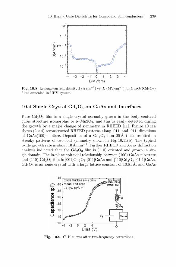
10 High κ Gate Dielectrics for Compound Semiconductors 239
−4 −3 −2 −1 0 1 2 3 4
10−8
10−6
1x10⁻⁴
10−2
100
J(A
/cm
2 )
E(MV/cm)
Fig. 10.8. Leakage current density J (A cm−2) vs. E (MV cm−1) for Ga2O3(Gd2O3)films annealed in UHV system
10.4 Single Crystal Gd2O3 on GaAs and Interfaces
Pure Gd2O3 film is a single crystal normally grown in the body centeredcubic structure isomorphic to α–Mn2O3, and this is easily detected duringthe growth by a major change of symmetry in RHEED [11]. Figure 10.11ashows (2× 4) reconstructed RHEED patterns along [011] and [011] directionsof GaAs(100) surface. Deposition of a Gd2O3 film 25 A thick resulted instreaky patterns of two fold symmetry shown in Fig. 10.11(b). The typicaloxide growth rate is about 10 Amin−1. Further RHEED and X-ray diffractionanalysis indicated that the Gd2O3 film is (110) oriented and grown in sin-gle domain. The in-plane epitaxial relationship between (100) GaAs substrateand (110) Gd2O3 film is [001]Gd2O3 [011]GaAs and [110]Gd2O3 [01 1]GaAs.Gd2O3 is an ionic crystal with a large lattice constant of 10.81 A, and GaAs
Fig. 10.9. C–V curves after two-frequency corrections

240 J. Kwo and M. Hong
0.2 0.4 0.6 0.8 1.0 1.2 1.4
1010
1011
1012
1013
1014
Dit(
cm−2
eV−1
)
EC-E (eV)
Fig. 10.10. Distribution of Dit vs. energy for Ga2O3(Gd2O3)/GaAs interface
is covalent bonding with a lattice constant of 5.65 A. The in-plane epitaxyof [100] of Gd2O3 being in parallel with [011] of GaAs suggests a super-celllattice match, i.e. the spacing of three Gd2O3 [100] lattices (32.4 A) matchedto that of four GaAs [011] lattices (32 A).
Interestingly when the film growth rate is lowered to ∼5 A min−1, thistransformation does not take place, and the film remains in the four foldsymmetry, the same as that of the substrate [20–22]. Figure 10.11c shows
Fig. 10.11. (a) (100) GaAs surface along [011] and [01 1] axes, (b) (110) cu-bic α-Gd2O3 film 25 A thick along [001] and [ 110] axes, and (c) (100) fluorite-related Gd2O3 film 18 A thick along the two highly symmetrical directions of [010]and [011]

10 High κ Gate Dielectrics for Compound Semiconductors 241
−10 −8 −6 −4 −2 0 2 4 6 8 1010
−12
1x10⁻¹⁰
1x10⁻⁸
1x10⁻⁶
1x10⁻⁴
1x10⁻²
1x100
1x10²−10 −8 −6 −4 −2 0 2 4 6 8 10
t=260At=185At=140At=104At=45At=25AGd2O3onSi, 40A
J L(A
/cm
2 )
E [MV/cm)
Fig. 10.12. Leakage current density JL vs. electrical field E for Gd2O3 films withdecreasing thickness
the RHEED patterns of such a film 18 A thick as the sample is rotated tomatch the in-plane [100] and [110] directions. X-ray analysis showed thatthe structure is consistent with a fully strained epitaxial film of Gd2O3 witha tetragonal unit cell of a = 5.65 A and c = 5.37 A. The unit cell is bestdescribed as a deformed fluorite-related structure under in-plane tensile straindue to the substrate epitaxy. This unit cell with 1/4 oxygen atom sites vacantis distorted to the extent that most of the atomic planes are not very welldefined.
The Gd2O3 dielectric films are highly electrically insulating, showing verylow leakage current densities of ∼10−9 to 10−10 Acm−2 at zero bias. This mayhave to do with that fact that Gd is electropositive +3 and has a strong affinityto oxygen. We measured the dependence of the leakage current density (JL)on the applied field (E) for a set of Gd2O3 samples with the oxide thickness (t)systematically reduced from 260 to 25 A (Fig. 10.12). The positive bias meansthat the metal electrode is positive with respective to GaAs. As t is decreasedfrom 260 to 45 A, the respective breakdown field Ebr increases systematicallyfrom 3 to 10 MV cm−1, yet JL increases merely by one order of magnitude.The maintenance of low electrical leakage even for films as thin as 25 A sug-gests that a high degree of structural integrity is sustained through epitaxy.Note that the leakage current density for the 25 A film is in mid 10−4 Acm−2
at 10 MVcm−1, and 10−4 Acm−2 at 7 MV cm−1. Considering the dielectricconstant of ∼14, the EOT of the 25 A film is ∼7 A. In comparison, the leak-age current density is 1A cm−2 at 7 MV cm−1 for an SiO2 film 15 A thick.Our results suggest that a thin and highly perfected single crystal oxide filmgives better dielectric characteristics over its amorphous counterpart, in termsof leakage currents and breakdown fields.

242 J. Kwo and M. Hong
Fig. 10.13. Drain I–V of inversion-channel enhancement-mode GaAs MOSFET’swith a gate dimension of 4 × 50 µm2
10.5 GaAs MOSFETs
10.5.1 Enhancement-Mode with Inversion
Since the carriers in this type of devices are confined to the top of GaAs,which is within 50–100 A near the oxide–GaAs interface, the interfacial rough-ness becomes a very important issue. Concerning the interaction betweenGa2O3(Gd2O3) and GaAs, which may occur during the high-temperatureanneal (>750 and >700C for implants of Si and Be, respectively) for activat-ing ion implants in the well, source and drain of the MOSFET, one approachin the device processing was taken by ion implantation on GaAs wafers, fol-lowed by activation annealing, and then gate-oxide deposition [13]. Duringthe high temperature anneal, however, the GaAs surface became rough andnot atomically ordered as observed using RHEED, despite extra efforts toprotect the surface. Even the surface of the device wafers was rough beforethe oxide deposition, p- and n-channel GaAs MOSFETs unexpectedly showedinversion. For the n-MOSFET, the gate voltage varies from 9 to 0 V in steps of−1 V and the VI is around 2 V. The saturation drain current is proportionalto (Vg–VI)2, typical characteristics of an enhancement-mode device with in-version. Figure 10.13 illustrates the drain I-V curves of such devices with adimension of 4 × 50 µm2. The p-MOSFET was operated as a three-terminaldevice and the gate voltage varies from −9 to 0 V in steps of 1 V (not shown).The threshold voltage, VI, is around −0.5V and the inversion channel is clearlydemonstrated. The magnitude of the maximum drain currents for both deviceswas low, in the range of 20–25 µA.
Since the free GaAs surface could not be maintained smooth during thehigh temperature annealing, another processing approach was employed, inwhich gate dielectrics were deposited on GaAs prior to the ion-implant, andactivation-annealing [14]. It was hoped that due to the thermodynamic sta-bility between Ga2O3(Gd2O3) and GaAs, the interface would remain smooth

10 High κ Gate Dielectrics for Compound Semiconductors 243
00 1 2 3 4 5 6
1
2
3
4
Vg=+3V
Vg=+5V
Vg=+7V
V=0V
Enhancement-Mode GaAs MOSFET
1 µmX100 µm Device
Dra
in C
urre
nt (
mA
)
Fig. 10.14. Drain I–V characteristics of inversion-mode n-channel GaAs MOSFETusing the second processing.
during the activation anneal at the high temperatures. With such a deviceprocessing, the drain current of an inversion n-channel GaAs MOSFET hasnow been increased to 3 mA for devices with 1 µm gate length. Figure 10.14shows typical drain current versus drain voltage characteristics of such a de-vice, with the gate voltage varying from 0 to 7 V in steps of 1 V. The maximumdrain current density and the extrinsic transconductance are 30 mA mm−1
and 4 mS mm−1, respectively. The increase in drain currents of the presentinversion-channel GaAs MOSFETs is more than 100 times over those of theprevious devices. CMOS circuits have also been demonstrated [28]. Effortsare now being taken to further increase the drain currents to the range of20–30 mA for 1 µm gate length devices. This is very likely judging from whathas been achieved in the inversion-channel InGaAs MOSFET’s on InP sub-strates [15]. Moreover, what we have recently accomplished in achieving anatomically smooth Ga2O3(Gd2O3)/GaAs interface during high temperatureannealing as discussed in Sect. 10.3 in this paper will make such devices areality.
10.5.2 Depletion-Mode MOSFET and Power Devices
GaAs MOSFETs feature a large logic swing, which gives a greater flexibilityfor digital IC designs. In contrast, GaAs metal-semiconductor FETs (MES-FETs) and high electron mobility transistors (HEMTs) exhibit small forwardgate voltages limited by the Schottky barrier heights. However, the drain cur-rent drift and hysteresis in the past has hindered the deployment of GaAsMOSFETs due to inadequate insulating films with significant bulk trappedcharges and a high Dit on GaAs [29,30]. Now with Ga2O3(Gd2O3) as the gatedielectric on GaAs, in which a Dit in the mid 1010 cm−2 eV−1 was attained,the depletion-mode MOSFET may show device performance not attainablepreviously. In this section, depletion-mode GaAs MOSFET’s of 0.8−µm gate-length, for the first time, exhibit negligible drain current drift and hysteresis.
Both drain and gate I–V characteristics of a 0.8 µm × 60 µm device areshown in Fig. 10.15, with the breakdown voltage of 24 V (corresponding to abreakdown field of 6.3 MV cm−1). The output characteristics measured with a

244 J. Kwo and M. Hong
Vg = +1V
Step= −0.5 VD
rain
Cur
rent
(m
A)
Drain Voltage (V)
0 1 2 3 4 5 60
5
10
15
20
25
30
35
40
45
50
toxide= 38 nm
−30 −20
1.00.80.60.40.20.0
−0.2
Gat
e C
urre
nt (
µA)
Gate Bias (V)
−0.4−0.6−0.8−1.0
−10 0 10 20 30
Fig. 10.15. Drain I–V characteristics of a 0.8 × 60 µm2 depletion mode GaAsMOSFET. Inset shows the gate I–V characteristics of such device
curve tracer show no I–V hysteresis and drain–current drift (not shown). Thedrain I–V characteristics are not sensitive to light, either. These observationsindicate insignificant bulk oxide trapped charges as well as a low Dit. The de-vice shows a clean pinch-off at a threshold voltage of −3.5V with the off-statedrain–source breakdown voltage of 12.5 V. Same threshold voltage was mea-sured in a quasi-dc condition. No discrepancy between I–V curves measuredunder quasi-dc condition and measured by 120 Hz curve tracer was found. Thevery high on-resistance ron was caused by high source resistances, which aredue to the low doping concentration (4 × 1017 cm−3) in the channel layer.The calculated effective channel mobility is 1,100 cm2 V−1 s−1. The maximumdrain current density (Imax) and the peak extrinsic transconductance (gm)are 450 mA mm−1 and 130 mS mm−1, respectively. The drain current den-sity as a function of gate bias in both forward and reverse sweep directionsshows negligible hysteresis, again indicating low mobile charge density and nocharge injection. The short-circuit current-gain cut-off frequency (fT) and themaximum oscillation frequency (fmax) were measured by biasing the devicesat Vds = 2V and Vgs = −1.5V. The fT = 17GHz and the fmax = 60GHzwere determined by extrapolating the short-circuit current-gain (H21) and themaximum stable gain (MSG) curves, respectively, using −20 dB per decadeslopes, as shown in Fig. 10.16. The long-term drain current drifting behaviorof the MOSFET was tested with the devices biasing at an extreme stress con-dition of Vds = 4 V and Vgs = +1V. No detectable short-term current driftwas observed in a period shorter than 1 s after the device was turned on. Thelong-term drain current drift is less than 1.5% during operation for a periodof over 150 h.
The GaAs depletion-mode MOSFTE’s with Ga2O3(Gd2O3) as gate di-electrics show excellent device performance, including long lifetime and for

10 High κ Gate Dielectrics for Compound Semiconductors 245
0.1 1 10 1000
10
20
30
40
50
60
Depletion - Mode GaAs MOSFET0.8 µm X 60 µm DeviceVds = 2V; Vgs =−1.5V
-20 dB/decadeMSG
H21
K
fT=17GHz
fmax=60 GHz
Frequency (GHz)
Gai
n (d
B)
0
1
2
3
4
5
6
K F
actor
Fig. 10.16. Microwave performance of the device in Fig. 10.15 measured at a drainvoltage of 2 V and a gate voltage of −15 V
the first time negligible hysteresis and drain current drift in the I-V character-istics. The flat transconductance profile reveals the advantage of MOSFET’sfor linearity consideration. These results present a significant advance towardsthe manufacture of commercially useful devices.
A power GaAs MOSFET (1 µm × 2.4 mm), measured from a curve traceroperating at 120 Hz, shows clean pinch-off drain current–voltage characteris-tics at a threshold voltage of −5V with no significant hysteresis [18]. The max-imum drain current density Imax and peak extrinsic transconductance gm are550 mA mm−1 and 125 mS mm−1, respectively. When measured at 850 MHzunder 3 V operation tuned for maximum output power, a peak power-addedefficiency (PAE) of 45% was obtained. Under the same condition, a lineargain GL = 20 dB and a saturated output power Psat = 23 dBm were mea-sured. When the drain bias increased to 5 V, the maximum PAE, GL, andPsat are 56%, 20 dB, and 26.5 dB m (power density=186 mW mm−1), respec-tively. The low doping concentration (2 × 1017 cm−3) in the channel layergives high contact resistance, which in turn results in the high on-resistanceron (5.1Ω · mm). It is expected that the PAE can be further improved by re-ducing the source and drain contact resistances as described earlier. A short-circuit current gain cutoff frequency fT of 15 GHz and a maximum oscillationfrequency fmax of 50 GHz were obtained from on-wafer S-parameter mea-surements of a 1 µm × 100 µm process control module. Larger devices (gateperiphery up to 2 cm) were also fabricated. However, the load impedances ofthose devices are too small (< 10 Ω), which are beyond the tuning range of ourload-pull system for optimum matching. Further improvement on PAE is ex-pected by reducing the contact resistance and optimizing the layer structure.
Recently, new depletion-mode GaAs and In015Ga085As/GaAs MOSFETs(with Ga2O3(Gd2O3) as a gate dielectric and a dimension of 1.6 µm×100 µm)were successfully fabricated. Well-behaved I–V characteristics were mea-sured for these devices. The strong accumulation current of 335 mA mm−1
at gate bias of 4 V and 510 mA mm−1 at 2 V of the depletion-mode GaAs
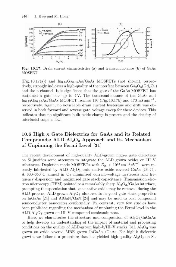
246 J. Kwo and M. Hong
L = 1.6µmW = 100µm
Fig. 10.17. Drain current characteristics (a) and transconductance (b) of GaAsMOSFET
(Fig. 10.17(a)) and In0.15Ga0.85As/GaAs MOSFETs (not shown), respec-tively, strongly indicates a high-quality of the interface between Ga2O3(Gd2O3)and the n-channel. It is significant that the gate of the GaAs MOSFET hassustained a gate bias up to 4 V. The transconductance of the GaAs andIn0.15Ga0.85As/GaAs MOSFET reaches 130 (Fig. 10.17b) and 170 mS mm−1,respectively. Again, no noticeable drain current hysteresis and drift was ob-served in both forward and reverse gate–voltage sweep for these devices. Thisindicates that no significant bulk oxide charge is present and the density ofinterfacial traps is low.
10.6 High κ Gate Dielectrics for GaAs and its RelatedCompounds: ALD Al2O3 Approach and its Mechanismof Unpinning the Fermi Level [31]
The recent development of high-quality ALD-grown high-κ gate dielectricson Si justifies some attempts to integrate the ALD grown oxides on III–Vsubstrates. Depletion mode MOSFETs with Dit < 1012 cm−2 eV−1 were re-cently fabricated by ALD Al2O3 onto native oxide covered GaAs [23, 24].A 600–650C anneal in O2 minimized current–voltage hysteresis and fre-quency dispersion, and maximized gate stack capacitance. Transmission elec-tron microscopy (TEM) pointed to a remarkably sharp Al2O3/GaAs interface,prompting the speculation that some native oxide may be removed during theALD process. ALD-grown Al2O3 also results in good gate stack propertieson InGaAs [24] and AlGaN/GaN [24] and may be used to coat compoundsemiconductor nano-wires conformally. By contrast, very few studies havebeen published regarding the mechanism of unpinning the Fermi level in theALD-Al2O3 grown on III–V compound semiconductors.
Here, we characterize the structure and composition of Al2O3/InGaAsto help develop an understanding of the impact of material and processingconditions on the quality of ALD-grown high-k/III–V stacks [31]. Al2O3 wasgrown on oxide-covered MBE grown InGaAs /GaAs. For high-k dielectricgrowth, we followed a procedure that has yielded high-quality Al2O3 on Si.

10 High κ Gate Dielectrics for Compound Semiconductors 247
Fig. 10.18. High-resolution cross sectional TEM picture of Al2O3 on In0.15Ga0.85
As after nitrogen annealing at 500C
Depositions were performed using alternating exposures of the common ALDprecursors Al(CH3)3 + H2O in a N2 carrier gas at 300C, using a Taiwan-made ALD reactor. Films were characterized by TEM, X-ray photoelectronspectroscopy (XPS), current–voltage (I–V ), and capacitance–voltage (C–V )measurement.
Figure 10.18 shows a high-resolution cross-section TEM picture of Al2O3/In02Ga08As/GaAs structure which was after 500C nitrogen annealing. Theoxide thickness measured by the TEM is 8 nm and a sharp transition fromInGaAs to Al2O3 was observed.
High-resolution X-ray photoelectron spectroscopy (XPS) using synchrotronradiation was performed to determine the interfacial chemistry. The XPS datawere taken at the U5 undulator beamline of National Synchrotron Radia-tion Research Center in Hsinchu, Taiwan. The U5 beamline operates overthe photon energies from 60 to 1,500 eV using a 6 m spherical grating mono-chromator with four interchangeable gratings. The energy resolving powerat 400 eV is better than 10,000 with slit openings set at 10 µm. Photoelec-trons were detected at a take-off angle of 53 with respect to the sam-ple surface by a PHI 279.4-mm diameter hemispherical electron analyzer.The pass energy of electron analyzer was fixed at 5.85 eV, and overall en-ergy resolution was better than 0.15 eV. Before measurements, the surfaceof samples was cleaned in situ by Ar+ sputtering at 500–1,000 eV primaryenergy.
Two samples, Al2O3/In0.2Ga0.8As/GaAs and InGaAs/GaAs, were studiedwith the latter as a reference (Fig. 10.19). The As 3d spectra for the as-grownAl2O3/In0.2Ga08As/GaAs showed a small, but very profound peak of As2O3.The peak quickly disappeared with a slight Ar+ sputtering, indicating a verysmall amount of arsenic oxides on top of the as-grown sample. There is nodetection of any arsenic oxides during the continuous sputtering. After theremoval of Al2O3 with sputtering, the peak belonging to InGaAs was revealed.
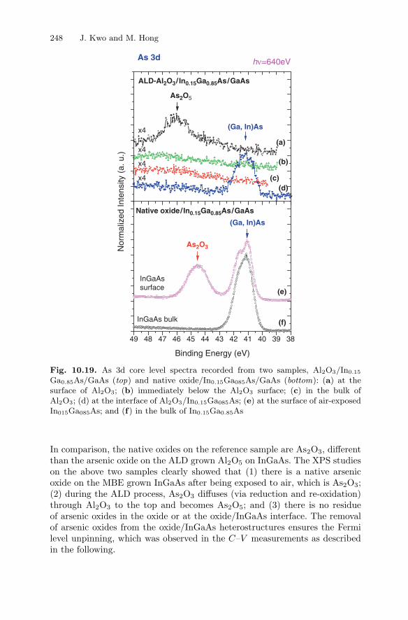
248 J. Kwo and M. Hong
49 48 47 46 45 44 43 42 41 40 39 38
InGaAssurface
(f)
(e)
(d)(c)
(b)
Native oxide/In0.15Ga0.85As/GaAs
ALD-Al2O3/In0.15Ga0.85As/GaAs
x4
x4
x4
x4
As2O5
As2O3
InGaAs bulk
As 3d
Binding Energy (eV)
Nor
mal
ized
Inte
nsity
(a.
u.)
hν=640eV
(Ga, In)As
(Ga, In)As
(a)
Fig. 10.19. As 3d core level spectra recorded from two samples, Al2O3/In0.15
Ga0.85As/GaAs (top) and native oxide/In0.15Ga085As/GaAs (bottom): (a) at thesurface of Al2O3; (b) immediately below the Al2O3 surface; (c) in the bulk ofAl2O3; (d) at the interface of Al2O3/In0.15Ga085As; (e) at the surface of air-exposedIn015Ga085As; and (f) in the bulk of In0.15Ga0.85As
In comparison, the native oxides on the reference sample are As2O3, differentthan the arsenic oxide on the ALD grown Al2O5 on InGaAs. The XPS studieson the above two samples clearly showed that (1) there is a native arsenicoxide on the MBE grown InGaAs after being exposed to air, which is As2O3;(2) during the ALD process, As2O3 diffuses (via reduction and re-oxidation)through Al2O3 to the top and becomes As2O5; and (3) there is no residueof arsenic oxides in the oxide or at the oxide/InGaAs interface. The removalof arsenic oxides from the oxide/InGaAs heterostructures ensures the Fermilevel unpinning, which was observed in the C–V measurements as describedin the following.

10 High κ Gate Dielectrics for Compound Semiconductors 249
Fig. 10.20. C–V curves of an MOS diode made of Au/Al2O3 (8.5 nm)/In015Ga085
As after two-frequency corrections in different thermal processes
The MOS diode structure was fabricated by evaporating Au dots 0.1 mmin diameter. I–V and C–V characteristics were measured using Agilent 4156Cand 4284, respectively. The dielectric constant of 8.5 nm Al2O3 is calculated tobe about 8.4 using the CV measurements (Fig. 10.20). Current density–voltage(J–V ) curves show a leakage current density of 8.5 nm Al2O3 on In0.15Ga0.85
As. Both as- and postannealing samples reveal leakage current about 10−8 to10−9 Acm−2 at a bias of 1 V (Fig. 10.21).
The Dit was calculated to be around 1012 cm−2 eV−1 at the midgap us-ing the Terman method as shown in Fig. 10.22. In comparison, the Dit fromGa2O3(Gd2O3) deposited on GaAs in UHV is one order of magnitude lowerin the range of ∼1011 cm−2 eV−1 [26]. The higher Dit in the ALD-Al2O3 onGaAs or InGaAs is probably caused by the existence of the native oxides of
−6 −4 −2 0 2 4 610−12
10−10
10−8
10−6
10−4
J (A
/cm
2 )
E (MV/cm)
no annealingoxygen annealing
Fig. 10.21. Leakage current density J (A/cm2) vs. E (MV cm−1) for Al2O3/In015Ga085As heterostructure in different thermal processes

250 J. Kwo and M. Hong
0.2 0.4 0.6 0.8 1.0 1.2 1.4
1011
1012
1013
1014
Dit
(cm
−2eV
−1)
EC−E
ALD-Al2O3/InGaAsGa2O3(Gd2O3)/GaAs
Fig. 10.22. Dit’s determined using the Terman Method for ALD- Al2O3/InGaAsand for UHV deposited Ga2O3(Gd2O3) on GaAs
In2O3 and Ga2O3 at the interface, while there are no such native oxides atthe UHV prepared Ga2O3(Gd2O3) on GaAs or InGaAs.
10.7 GaN Passivation
We now turn to a brief discussion of the epitaxial growth of the rare earthoxide films on GaN for surface pssivation [32]. RHEED patterns in Fig. 10.23upper panel are the UHV annealed GaN surface of sixfold symmetry alongthe 〈100〉 and 〈110〉 azimuthal direction with a 30 separation. During theinitial growth of Gd2O318 A thick on GaN, intense and streaky RHEED pat-terns of sixfold symmetry were observed, indicating a smooth two-dimensionalgrowth. The two major in-plane directions of the oxide, separated by 30
in Fig. 10.23 lower panel are aligned with those of GaN. This is in sharpcontrast to the two- and fourfold symmetry observed in the growth ofGd2O3 on GaAs.
X-ray diffraction studies show that Gd2O3 grows epitaxially on GaN ina hexagonal phase (Fig. 10.24), rather than the common cubic phase ob-served in case of rare earth oxides on GaAs or Si [32]. Despite a large latticemismatch between the hexagonal rare earth oxides and the wurtzite GaN,the epitaxy occurs in the very initial stage of the film growth, and thereis no in-plane rotation between the rare earth oxides and GaN. The bulkvalues of in- and out-of-plane lattice constants for hexagonal GaN shownin Fig. 10.25 are 3.189 and 5.185 A, respectively. Those for bulk hexagonalGd2O3 are 3.86 and 6.16 A, respectively (Fig. 10.26) [33]. The in-plane latticeconstant of the Gd2O3 films 18 A thick is close to the bulk value, indicatingthat the Gd2O3 film was relaxed and not constrained to the GaN. Gd2O3
and Y2O3 appear to wet the GaN surface very well, despite the large lattice

10 High κ Gate Dielectrics for Compound Semiconductors 251
Fig. 10.23. (upper) RHEED patterns of GaN surface and (lower) RHEED of Gd2O3
film 18 A thick deposited on GaN
mismatch. These thin epitaxial oxide films are fully relaxed and are of excel-lent structural quality, indicating that misfit dislocations are trapped near theinterface.
We have obtained a low Dit of ∼1011 cm−2 eV−1 from the capacitance–voltage data for the rare earth oxide/GaN interface [34]. The attainment ofa low interfacial density of states is critical to the passivation of the GaNsurface to reduce the surface state density, and to improve the lifetime ofthe MESFET and HEMT devices for electronic and optoelectronic applica-tions. Furthermore, we have successfully carried out the overgrowth of singlecrystalline GaN film on Gd2O3/GaN after ex situ transferring to another MBEsystem [35]. A polycrystalline growth of preferred orientation was observedduring the initial overgrowth of GaN on the rare earth oxides. The GaN filmsurface then becomes smoother and better ordered in the hcp wurtzite struc-ture as the film grows thicker. Again, there was no inplane rotation betweenGaN and the oxide underneath.
Fig. 10.24. X-ray diffraction normal scan on the Gd2O3 film as discussed inFig. 10.23

252 J. Kwo and M. Hong
Fig. 10.25. Structure and stacking sequence of the wurtzite GaN hcp phase
In the area of GaN surface passivation, research efforts of depositing orgrowing insulators (and methods to prepare them) on GaN to give a low Dit
at the insulator/GaN interface have shown that appropriate insulators andproper steps for cleaning GaN surfaces are critical to achieve a low Dit. GaNsurfaces are not as robust and inert as generally thought when exposed toatmosphere such as room air. A summary of the efforts was given in a reviewarticle [36]. Cleaning procedures for preparing GaN surfaces for deposition ofinsulators are also included in the reference. Among the insulating materialsbeing studied for GaN passivation, AlN, rare earth oxide Gd2O3, and Sc2O3
Fig. 10.26. Structure and stacking sequence of the hcp rare earth Gd2O3
sesquioxide

10 High κ Gate Dielectrics for Compound Semiconductors 253
are single crystals. Previously, Sc2O3 was found to effectively passivate GaN[37] and to grow single crystal on GaN and sapphire (Al2O3), but with thein-plane growth in two degenerate orientations [38].
However, we have also achieved an excellent epitaxial growth of single-domain, single-crystal Sc2O3 films on Si(111), an unexpected result [39].The structural perfection of the Sc2O3 films 3 and 18 nm thick is evi-denced from very bright streaky and reconstructed RHEED patterns, verynarrow rocking curves in the high-resolution x-ray diffraction, and a flatsmooth film both at the interface and in the film interior observed usingX-ray reflectivity and HR-TEM. Decent electrical characteristics of the ox-ide film were measured with a low leakage current and a high breakdownof >5MV cm−1.
10.8 Conclusion
We have given a review on some of the important recent work on high κgate dielectrics on compound semiconductors. Ga2O3(Gd2O3), the novel ox-ide, which was electron-beam evaporated from a gallium–gadollium–garnettarget in UHV, has unpinned the GaAs Fermi level for the first time. System-atic heat treatments under various gases were studied to achieve low leakagecurrents and low Dit’s. Thermodynamic stability of the Ga2O3(Gd2O3)/GaAsheterostructures and the interfaces were achieved with high temperature an-nealing, which is needed for fabricating inversion-channel MOSFET’s. Moreimportantly, Ga2O3(Gd2O3) remains amorphous and the interface remains in-tact with atomic smoothness and sharpness. Single crystal Gd2O3 was foundto grow epitaxially on GaAs, for the first time, single crystal oxide epitaxiallygrown on single crystal semiconductor with excellent electrical properties anddevice performance. We have studied the mechanism of Fermi-level unpinningin ALD-Al2O3 ex-situ deposited on GaAs (InGaAs). Note that ALD is com-monly used to deposited high-k gate dielectrics such as Al2O3 and HfO2 onSi. We have also reviewed the work of inversion-channel, depletion-mode, andpower GaAs MOSFETs using Ga2O3(Gd2O3) as the gate dielectric. Finally,we have discussed the work of GaN passivation using single crystal rare earthof Gd2O3, which will play an important role in high temperature and highpower electronic device application.
Acknowledgments
The authors thank Department of Nature Sciences at National Science Coun-cil, Taiwan, Republic of China for supporting our work on high-k gate di-electrics. We also thank the discussion with our able student Y.C. Chang.

254 J. Kwo and M. Hong
References
1. D.A. Muller, T. Sorsch, S. Moccio, F.H. Baumann, and G. Timp, Nature, 399,758, (1999).
2. For a complete review, Materials Research Bulletin, March 2002 issue, on “Al-ternative Gate Dielectric for Microelectronics”, Ed. by R.M. Wallace and G.D.Wilk.
3. J. Kwo, M. Hong, A.R. Kortan, K.L. Queeney, Y.J. Chabal, J.P. Mannaerts,T. Boone, J.J. Krajewski, A.M. Sergent, and J.M. Rosamilia, Appl. Phys. Lett.77, 130, (2000).
4. J. Kwo, M. Hong, A.R. Kortan, K.L. Queeney, Y.J. Chabal, R.L. Opila, Jr.,D.A. Muller, et al., J. Appl. Phys. 89, 3920, (2001).
5. B.W. Busch, J. Kwo, M. Hong, J.P. Mannaerts, and B.J. Sapjeta, W.H. Schulte,E. Garfunkel, and T. Gustafsson, Appl. Phys. Lett. 79, 2447, (2001).
6. J. Kwo, M. Hong, B. Busch, D.A. Muller, Y.J. Chabal, A.R. Kortan, J.P. Man-naerts, B. Yang, P. Ye, H. Gossmann, A.M. Sergent, K.K. Ng, J. Bude, W.H.Schulte, E. Garfunkel, and T. Gustafsson, J. Crystal Growth, 251, 645, (2003).
7. “High κ Gate Dielectrics For Si and Compound Semiconductors By MBE”, J.Kwo and M. Hong, MRS Proceeding, Vol. 745, (2003).
8. “Semiconductor-insulator interfaces”, M. Hong, C.T. Liu, H. Reese, and J. Kwoin “Encyclopedia of Electrical and Electronics Engineering”, Vol. 19, pp. 87–100, Ed. J.G. Webster, Wiley, New York, 1999, and references therein.
9. “Phys. & Chem. of III–V Compound Semiconductor Interfaces”, Ed. by C.W.Wilmsen, Plenum, New York, 1985.
10. M. Hong, M. Passlack, J.P. Mannaerts, J. Kwo, S.N.G. Chu, N. Moriya, S.Y.Hou, and V.J. Fratello, J. Vac. Sci. Technol. B 14(3), May/Jun, 2297, (1996).
11. M. Hong, J. Kwo, A.R. Kortan, J.P. Mannaerts, and A.M. Sergent, Science,283, pp. 1897–1900, (1999).
12. M. Passlack, M. Hong, and J.P. Mannaerts, Appl. Phys. Lett. 68(8), 1099,(1996).
13. F. Ren, M. Hong, W.S. Hobson, J.M. Kuo, J.R. Lothian, J.P. Mannaerts, J.Kwo, Y.K. Chen, and A.Y. Cho, IEEE Int. Electron Dev. Mtg (IEDM) TechnicalDigest, p.943, (1996), and also in Solid State Electron., 41 (11), 1751, (1997).
14. Y.C. Wang, M. Hong, J.M. Kuo, J.P. Mannaerts, J. Kwo, H.S. Tsai, J.J. Kra-jewski, J.S. Weiner, Y.K. Chen, and A.Y. Cho, Mater. Res. Soc. Symp. Proc.573, 219, (1999).
15. F. Ren, J.M. Kuo, M. Hong, W.S. Hobson, J.R. Lothian, J. Lin, W.S. Tseng,J.P. Mannaerts, J. Kwo, S.N.G. Chu, Y.K. Chen, and A.Y. Cho, IEEE ElectronDevice Lett., 19(8), 309, (1998).
16. F. Ren, M. Hong, S.N.G. Chu, M.A. Marcus, M.J. Schurman, A. Baca S.J.Pearton, and C.R. Abernathy, Appl. Phys. Lett., 73, 3893–3895, (1998).
17. Y.C. Wang, M. Hong, J.M. Kuo, J.P. Mannaerts, J. Kwo, H.S. Tsai, J.J. Kra-jewski, Y.K. Chen, and A.Y. Cho, IEEE Int. Electron Devices Mtg (IEDM)Technical Digest, 67, (1998), and also in Electron Dev. Lett., 20, 457, (1999).
18. Y.C. Wang, M. Hong, J.M. Kuo, J.P. Mannaerts, H.S. Tsai, J. Kwo, J.J. Kra-jewski, Y.K. Chen, and A.Y. Cho, Electron. Lett., 35(8), 667, April 15th (1999).
19. M. Hong, Z.H. Lu, J. Kwo, A.R. Kortan, J.P. Mannaerts, J.J. Krajewski, K.C.Hsieh, L.J. Chou, and K.Y. Cheng, Appl. Phys. Lett. 76(3), 312, (2000).

10 High κ Gate Dielectrics for Compound Semiconductors 255
20. A.R. Kortan, M. Hong, J. Kwo, J.P. Mannaerts, J.J. Krajewski, N. Kopylov,C. Steiner, B. Bolliger, and M. Erbudak, J. Vac. Sci. Technol. B 19(4), 1434,(2001).
21. M. Sowwan, Y. Yacoby, J. Pitney, R. MacHarrie, M. Hong, J. Cross, D.A. Walko,R. Clarke, R. Pindak, and E.A. Stern, Phys. Rev. B 66, 205311, (2002).
22. Y. Yacoby, M. Sowwan, E. Stern, J. Cross, D. Brewe, R. Pindak, J. Pitney, E.Dufresne, and R. Clarke, Nat. Mater. 1, 99, (2002).
23. P.D. Ye, G.D. Wilk, B. Yang, J. Kwo, S.N.G. Chu, S. Nakahara, H.-J.L. Goss-mann, J.P. Mannaerts, M. Hong, K.K. Ng, and J. Bude, Appl. Phys. Lett. 83,180, (2003).
24. M.M. Frank, G.D. Wilk, D. Starodub, T. Gustafsson, E. Garfunkel, Y.J. Chabal,J. Grazul, and D.A. Muller, Appl. Phys. Lett. 86, 152904, (2005), and referencestherein.
25. J. Kwo, M. Hong, J.P. Mannaerts, Y.D. Wu, K.Y. Lee, B. Yang, and T. Gustafs-son, in Integration of Advanced Micro- and Nanoelectronic Devices—CriticalIssues and Solutions, Ed. by J. Morais, D. Kumar, M. Houssa, R.K. Singh, D.Landheer, R. Ramesh, R.M. Wallace, S. Guha, and H. Koinuma (Mater. Res.Soc. Symp. Proc. 811, Warrendale, PA, 2004), E1.12. (MRS Spring Meeting2004.).
26. Y.L. Huang, P. Chang, Z.K. Yang, Y.J. Lee, H.Y. Lee, H.J. Liu J. Kwo, J.P.Mannaerts, and M. Hong, Appl. Phys. Lett. 86, 191905, 2005, and referencestherein.
27. M. Hong, Z.H. Lu, J. Kwo, A.R. Kortan, J.P. Mannaerts, J.J. Krajewski, K.C.Hsieh, L.J. Chou, and K.Y. Cheng, Appl. Phys. Lett. 76 (3), 312, (2000).
28. M. Hong, J.N. Baillargeon, J. Kwo, J.P. Mannaerts, and A.Y. Cho, Proceedingsof 2000 IEEE International Symposium on Compound Semiconductors, 345,00TH 9498.
29. T. Mimura and M. Fukuta, IEEE Trans. Electron Dev., 27(6), 1147, (1980).30. D.S.L. Mui, Z. Wang, and H. Morkoc, Thin Solid Films, 231, 107, (1993).31. M.L. Huang, Y.C. Chang, C.H. Chang, Y.J. Lee, P. Chang, J. Kwo, T.B. Wu,
and M. Hong, Appl. Phys. Lett. 87, 252104, 2005.32. M. Hong, A.R. Kortan, J. Kwo, J.P. Mannaerts, C.M. Lee, and J. I. Chyi, in
IEEE International Symposium on Compound Semiconductors, IEEE Publica-tion Series 00TH8498, 495, (2000).
33. L. Pauling, Z. Kristallogr, 69, 415, (1928).34. T.S. Lay, W.D. Liu, M. Hong, J. Kwo, and J.P. Mannaerts, Electronics Letters,
37, 595, (2001).35. M. Hong, A.R. Kortan, H.M. Ng, J. Kwo, S.N.G. Chu, J.P. Mannaerts, A.Y.
Cho, C.M. Lee, J.I. Chyi, and K.A. Anselm, 20th NA MBE October 1–3, 2001,J. Vac. Sci.Technol. B 20, 1274, (2002).
36. M. Hong, H.M. Ng, J. Kwo, A.R. Kortan, J.N. Baillargeon, S.N. G. Chu, J.P.Mannaerts, A.Y. Cho, F. Ren, C.R. Abernathy, S. J. Pearton, and J.I. Chyi, In-vited talk at 197th Electrochemical Society Meeting, Toronto, Ontario, Canada,May 14-19, 2000. The paper is on p. 103 of “Compound semiconductor powertransistors II and state-of-the-art program on compound semiconductors (SO-TAPOCS XXXII), Ed. by R. Kopf, A.G. Baca, and S.N.G. Chu ECS Proc.volume 2000–1.
37. B. Luo, J.W. Johnson, J. Kim, R.M. Mehandru, F. Ren, B.P. Gila, A.H. Onstine,C.R. Abernathy, and S.J. Pearton, A.G. Baca, R.D. Briggs, R.J. Shul, and C.Monier, J. Han, App. Phys. Lett. 80, 1661 (2002).
256 J. Kwo and M. Hong
38. A.R. Kortan, M. Hong, J. Kwo, P. Chang, C.P. Chen, J.P. Mannaerts, and S.H.Liou, in Integration of Advanced Micro- and Nanoelectronic Devices—CriticalIssues and Solutions, Ed. by J. Morais, D. Kumar, M. Houssa, R.K. Singh, D.Landheer, R. Ramesh, R.M. Wallace, S. Guha, and H. Koinuma (Mater. Res.Soc. Symp. Proc. 811, Warrendale, PA , 2004), p. E1.2. (MRS Spring Meeting2004.).
39. C.P. Chen, M. Hong, J. Kwo, H.M. Cheng, Y.L. Huang, S.Y. Lin, J. Chi, H.Y.Lee, Y.F. Hsieh, and J.P. Mannaerts, J. Cryst. Growth 278, 638–642, (2005).
11
Interface Properties of High-kDielectrics on Germanium
A. Toriumi, K. Kita, M. Toyama, and H. Nomura
Summary. Ge CMOS with high-k dielectric films is very attractive as one of thepost-Si device candidates with low-power as well as high-performance. The most im-portant issue for Ge CMOS technology is how to achieve a superior-quality interfacebetween the high-k dielectric film on Ge. This chapter first describes the effects thatGeOx volatility during the high-k film growth process have on Ge. Another inter-esting feature of the high-k/Ge interface is the effect that Ge surface orientation hason interface properties. Finally, HfO2 and Y2O3 on Ge are compared and discussedin terms of the interface quality of high-k on Ge.
11.1 Introduction
Although Ge CMOS devices have historically been left behind the recentresearch has brought them to the forefront again due by Si field effect devicesto the trend of using deposited high-k films instead of thermally grown SiO2
to achieve further CMOS scaling. This is very attractive because of bothGe’s intrinsically higher carrier mobilities in part than those of Si, which canprovide a larger driving current, and its smaller band gap to enable operationat a lower voltage. In addition, high-k dielectrics are needed irrespective of thechannel materials to reduce the gate leakage current for lower-power operation.However, the challenges actually posed by high-k/Ge CMOSs are still poorlyunderstood.
The interface layer in a high-k/Ge system is associated with GeOx growth,the same as for the high-k/Si interface in an O2 ambient, although it has beenreported that GeOx on Ge is thermally unstable and worse in electrical char-acteristics compared with SiOx grown on Si. We have recently found that MIScapacitors with no interface layer can be achieved in a high-k/Ge system [1].There are, however, concerns that electrical characteristics strongly depend onthe interfacial properties as well as the high-k materials employed. Therefore,we urgently need to select high-k materials that form a good interface withGe.

258 A. Toriumi et al.
Careful development of (100) Si substrates has been necessary to achieveindustrial application of Si microelectronics. This should also be the case forGe devices. Here, we report distinct differences in the surface chemistry of(111) and (100) Ge surfaces in terms of the oxidation rate, surface rougheningeffect, and MIS capacitor characteristics. Based on the results, we discussthe advantages of the (111) Ge surface. It is also important to investigatewhich high-k material is suitable for Ge devices. We report that Y2O3 formsan excellent interface with Ge in contrast with HfO2. We do not intend toanalyse the experimental results in great detail in this chapter but would liketo show new findings on Ge interface-related characteristics.
11.2 Experimental
Three kinds of experimental results are presented in this chapter. HfO2
films were processed on Ge and Si wafers simultaneously for comparison,except for the wafer cleaning steps. The Ge wafers were degreased withmethanol, immersed in HCl solution to remove the native oxides, and re-oxidized in H2O2 solution, which was followed by dipping in diluted HF so-lution and rinsing in deionized water. Almost no Ge oxides were left on theGe surface after these cleaning steps, which was confirmed by X-ray pho-toelectron spectroscopy (XPS) measurements. The Si wafers were cleanedwith H2SO4/H2O2 and HCl/H2O2 solutions, and immersed in diluted HFsolution.
In the first experiment, HfO2 films (2–15 nm-thick) were deposited in atwo-step sputtering process for the Hf metal target. A 1.5-nm-thick Hf metallayer was deposited in Ar, followed by reactively sputtering Hf metal in O2/Ar.The ultra-thin metallic Hf layer was expected to be oxidized during the reac-tive sputtering to restrict the growth of the interface layer. For comparison,HfO2 films without pre-depositing metallic Hf layers were also prepared. Thefilms on both substrates were simultaneously annealed in O2(0.1%) + N2 at400 and 500C. The interface layer and HfO2 thicknesses were determined byboth cross-sectional transmission electron microscopy (TEM) and the com-bination of glazing incidence X-ray reflectivity (GIXR) with spectroscopicellipsometry (SE) measurements [2].
In the second experiment, the differences in the oxidation rates between(100) and (111) Ge wafers were investigated. Moreover, HfO2 films were de-posited on (100) and (111) Ge wafers by reactive sputtering and investigatedin terms of thermal stability and interface quality, because there has been no apriori consensus on an appropriate surface orientation for device applications,though there have been debates on the optimum surface orientation from thedevice performance viewpoint [3, 4].
In the third experiment, we prepared HfO2/Ge and Y2O3/Ge MIS capac-itors to study suitable high-k films on the (100) Ge substrate. We deposited5 nm-thick Y2O3 or HfO2 films by rf-sputtering on p- (100) Ge wafers, and
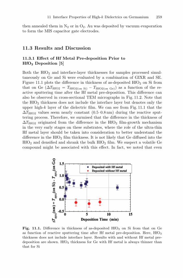
11 Interface Properties of High-k Dielectrics on Germanium 259
then annealed them in N2 or in O2. Au was deposited by vacuum evaporationto form the MIS capacitor gate electrodes.
11.3 Results and Discussion
11.3.1 Effect of Hf Metal Pre-deposition Prior toHfO2 Deposition [5]
Both the HfO2 and interface-layer thicknesses for samples processed simul-taneously on Ge and Si were evaluated by a combination of GIXR and SE.Figure 11.1 plots the difference in thickness of as-deposited HfO2 on Si fromthat on Ge (∆THfO2 = THfO2(on Si) − THfO2(on Ge)) as a function of the re-active sputtering time after the Hf metal pre-deposition. This difference canalso be observed in cross-sectional TEM micrographs in Fig. 11.2. Note thatthe HfO2 thickness does not include the interface layer but denotes only theupper high-k layer of the dielectric film. We can see from Fig. 11.1 that the∆THfO2 values seem nearly constant (0.5–0.8 nm) during the reactive sput-tering process. Therefore, we surmised that the difference in the thickness of∆THfO2 originated from the difference in the HfO2 film-growth mechanismin the very early stages on these substrates, where the role of the ultra-thinHf metal layer should be taken into consideration to better understand thedifference in the HfO2 film thickness. It is not likely that Ge diffused into theHfO2 and densified and shrank the bulk HfO2 film. We suspect a volatile Gecompound might be associated with this effect. In fact, we noted that even
Fig. 11.1. Difference in thickness of as-deposited HfO2 on Si from that on Geas function of reactive sputtering time after Hf metal pre-deposition. Here, HfO2
thickness does not include interface layer. Results with and without Hf metal pre-deposition are shown. HfO2 thickness for Ge with Hf metal is always thinner thanthat for Si

260 A. Toriumi et al.
Fig. 11.2. Cross-sectional TEM micrographs of both (a) HfO2/Ge and (b) HfO2/Sideposited by reactive sputtering in Ar/O2 after Hf metal pre-deposition. Schematicsare also shown. Note that the upper HfO2 thicknesses are different despite HfO2
being deposited simultaneously in this experiment
without annealing, HfO2 films on Ge were also thinner than those on Si, whichsuggests that Hf–Ge–O volatilization occurs not during thermal-annealing butduring the film-deposition processes. Although the mixing process of Hf withGe and/or O may explain the substantial interface layer thickness reduction,the change in upper high-k layer thickness is hard to be understood. So, itis likely that the volatilization of Ge oxides may be enhanced by the pres-ence of the Hf metal acting as a catalyst, since GeOx volatilization will notoccur under moderate pressure at room temperature. Chui et al. reportedthat they had observed no Ge oxides at the ZrO2/Ge interface after the UV-ozone low-temperature oxidation of a metallic Zr layer on Ge [6], and wenoted from our present results that the thickness of upper HfO2 film was alsoaffected by the growth conditions during the reactive sputtering depositionprocess. Furthermore, the difference of HfO2 film growth on both Ge and Sisubstrates in the initial stages of the reactive sputtering process can be seen inFig. 11.3. Film growth on the Ge substrate clearly reveals a retardation at thebeginning of reactive sputtering, contrary to monotonic film growth on theSi substrate. The retarded film growth on Ge is consistent with our reactionmodel, if the desorption of Hf–Ge–O compounds is assumed to occur onlybefore the ultra-thin metallic Hf layer is fully oxidized. These results stronglysuggest that Hf–Ge–O volatilization may be involved in the very early stagesof film growth during the reactive sputtering process of HfO2, and that theGe interface needs to be treated more carefully than the Si one.
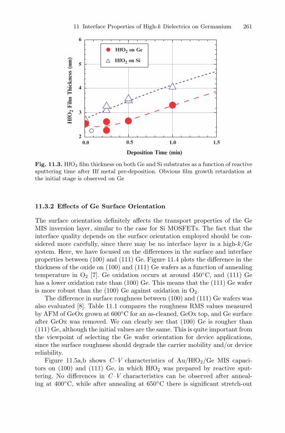
11 Interface Properties of High-k Dielectrics on Germanium 261
20.0 0.5 1.0
Deposition Time (min)
HfO
2 Film
Thi
ckne
ss (
nm)
1.5
3
4
5
6
HfO2 on Ge
HfO2 on Si
Fig. 11.3. HfO2 film thickness on both Ge and Si substrates as a function of reactivesputtering time after Hf metal pre-deposition. Obvious film growth retardation atthe initial stage is observed on Ge
11.3.2 Effects of Ge Surface Orientation
The surface orientation definitely affects the transport properties of the GeMIS inversion layer, similar to the case for Si MOSFETs. The fact that theinterface quality depends on the surface orientation employed should be con-sidered more carefully, since there may be no interface layer in a high-k/Gesystem. Here, we have focused on the differences in the surface and interfaceproperties between (100) and (111) Ge. Figure 11.4 plots the difference in thethickness of the oxide on (100) and (111) Ge wafers as a function of annealingtemperature in O2 [7]. Ge oxidation occurs at around 450C, and (111) Gehas a lower oxidation rate than (100) Ge. This means that the (111) Ge waferis more robust than the (100) Ge against oxidation in O2.
The difference in surface roughness between (100) and (111) Ge wafers wasalso evaluated [8]. Table 11.1 compares the roughness RMS values measuredby AFM of GeOx grown at 600C for an as-cleaned, GeOx top, and Ge surfaceafter GeOx was removed. We can clearly see that (100) Ge is rougher than(111) Ge, although the initial values are the same. This is quite important fromthe viewpoint of selecting the Ge wafer orientation for device applications,since the surface roughness should degrade the carrier mobility and/or devicereliability.
Figure 11.5a,b shows C–V characteristics of Au/HfO2/Ge MIS capaci-tors on (100) and (111) Ge, in which HfO2 was prepared by reactive sput-tering. No differences in C–V characteristics can be observed after anneal-ing at 400C, while after annealing at 650C there is significant stretch-out

262 A. Toriumi et al.
(100) with GIXR
GeO
2 T
hick
ness
(nm
)
Ge (100)Ge (100)Ge (100)Ge (111)Ge (111)Ge (111)
40
30
20
10
0350 400 450 500 550 600 650
Anneal Temperature (°C)
(100) with Ellipsometry(111) with GIXR
(111) with Ellipsometry
Fig. 11.4. GeOx thickness on (100) and (111) Ge wafers as a function of oxidationtemperature. Thickness was determined independently by GIXR and SE
in C–V curves for HfO2/(100) Ge both in 1-kHz and 1-MHz measurements.Although C–V hysteresis was observed in the results, they are not shown herefor clear comparison between the two different substrate orientations. In ad-dition, one should note that the saturated capacitance on (111) Ge is higherthat that on (100) Ge. This indicates that the interface on (100) Ge is de-graded more severely (imperfectly oxidized) compared to that on (111) Ge interms of electrical properties as well as surface morphology. Furthermore, thestretch-out becomes worse at higher annealing temperatures. The microscopicmechanism responsible for the surface orientation dependence of degradationis now under investigation.
11.3.3 Y2O3 and HfO2 on (100) Ge [9,10]
The interface quality is expected to depend on the high-k materials employed.We compared two kinds of high-k materials on (100) Ge from the viewpoint ofMIS capacitor characteristics. Figure 11.6a plots both the thicknesses of theupper high-k and interface layers as a function of the annealing temperaturein N2. In both Y2O3 and HfO2 cases, the high-k layer thicknesses are almostconstant, while no interface layers are identified above annealing at 400C. The
Table 11.1. Roughness RMS values measured by AFM for as-cleaned, GeOx top,and Ge surface after removing GeOx
Ge surface As-cleaned (nm) Oxide top (nm) Ge top (nm)
(100) 0.22 ± 0.01 0.71 ± 0.06 0.28 ± 0.03(111) 0.22 ± 0.02 0.58 ± 0.03 0.15 ± 0.01

11 Interface Properties of High-k Dielectrics on Germanium 263
1x10⁻⁶ 3x10⁻⁷
2x10⁻⁷
1x10⁻⁷
0−2 −1 0 1 2
1kHz
1kHz
00
(a) 400 °C (b) 650 °C
1 2−2 −1
1MHz1MHz
Cap
acit
ance
(F
/cm
2 )
Cap
acit
ance
(F
/cm
2 )
Gate Voltage (V) Gate Voltage (V)
8x10⁻⁷
6x10⁻⁷
4x10⁻⁷
2x10⁻⁷
Ge (111)Ge (111)
Ge (100)Ge (100)
Ge (100)Ge (100)
Ge (111)
Ge (100)
Ge (100)
Ge (111)
Fig. 11.5. Comparison of high frequency C–V characteristics of Au/HfO2/Ge MIScapacitors on (100) and on (111) Ge wafers, annealed at (a) 400C, and (b) 650C,in O2 for 30 s
TEM micrograph in Fig. 11.6b shows direct evidence of an abrupt interfaceat the Y2O3/Ge boundary annealed at 600C in N2. Thus, we conclude thatthe interface layers in Y2O3/Ge and HfO2/Ge stacks disappeared due to thereaction between high-k films and GeOx. This is one advantage of sputter-deposited high-k/Ge systems in terms of EOT scaling.
We next discuss the MIS capacitor characteristics of Au/Y2O3/Ge andAu/HfO2/Ge capacitors. Figure 11.7 plots the high frequency C–V character-istics of Y2O3/Ge and HfO2/Ge MIS capacitors annealed in N2 at 600C at1 MHz at 300 K. The C–V characteristics of the Y2O3/Ge MIS capacitors seemmuch better than those of the HfO2/Ge system. This indicates that Y2O3/Ge
Y2O3/Ge ILHfO2/Ge IL
HfO2/Ge HfO2 filmY2O3/Ge Y2O3 film
Annealing Temperature (°C)
(a) (b)
Th
ickn
ess
(nm
)
6
4
2
0
As-depo 400 500 600−2
Fig. 11.6. (a) Thicknesses of upper high-k and interface layers as function of an-nealing temperature in N2. (b) TEM micrograph of abrupt interface at Y2O3/Geannealed at 600C in N2 showing direct evidence of no interface layer
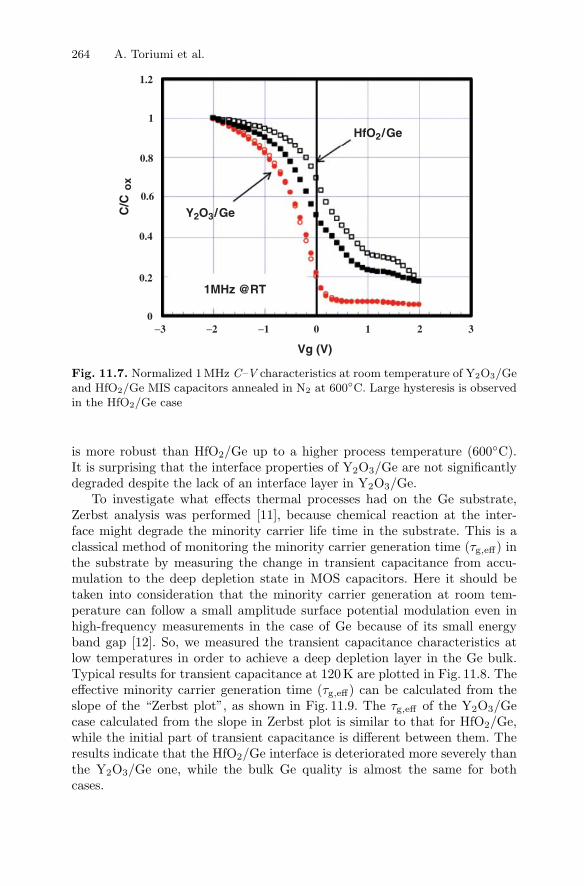
264 A. Toriumi et al.
1.2
0.8
0.6
0.4
0.2
0−3 −2 −1 0
Vg (V)
HfO2/Ge
Y2O3/Ge
1MHz @RT
C/C
ox
1 2 3
1
Fig. 11.7. Normalized 1 MHz C–V characteristics at room temperature of Y2O3/Geand HfO2/Ge MIS capacitors annealed in N2 at 600C. Large hysteresis is observedin the HfO2/Ge case
is more robust than HfO2/Ge up to a higher process temperature (600C).It is surprising that the interface properties of Y2O3/Ge are not significantlydegraded despite the lack of an interface layer in Y2O3/Ge.
To investigate what effects thermal processes had on the Ge substrate,Zerbst analysis was performed [11], because chemical reaction at the inter-face might degrade the minority carrier life time in the substrate. This is aclassical method of monitoring the minority carrier generation time (τg,eff) inthe substrate by measuring the change in transient capacitance from accu-mulation to the deep depletion state in MOS capacitors. Here it should betaken into consideration that the minority carrier generation at room tem-perature can follow a small amplitude surface potential modulation even inhigh-frequency measurements in the case of Ge because of its small energyband gap [12]. So, we measured the transient capacitance characteristics atlow temperatures in order to achieve a deep depletion layer in the Ge bulk.Typical results for transient capacitance at 120 K are plotted in Fig. 11.8. Theeffective minority carrier generation time (τg,eff) can be calculated from theslope of the “Zerbst plot”, as shown in Fig. 11.9. The τg,eff of the Y2O3/Gecase calculated from the slope in Zerbst plot is similar to that for HfO2/Ge,while the initial part of transient capacitance is different between them. Theresults indicate that the HfO2/Ge interface is deteriorated more severely thanthe Y2O3/Ge one, while the bulk Ge quality is almost the same for bothcases.

11 Interface Properties of High-k Dielectrics on Germanium 265
3
2.5
1.5
10 200 400 600 800 1000
2
C (
pF
)
Time (sec)
@ 120k
Y2O3/Ge
HfO2/Ge
Fig. 11.8. Transient capacitance characteristics when gate bias was changed fromaccumulation to inversion at 120K both for Y2O3/Ge and HfO2/Ge MIS capacitors
1000
HfO2/Ge
T=120K
Y2O3/Ge
800
600
400
200
0
0.0 0.1 0.2 0.3 0.4 0.5
−d(C
ox/
C)2
/dt
Cinv/C−1
Fig. 11.9. Low temperature Zerbst plots for transient capacitance results inFig. 11.8. It is noticed that a difference of the initial transient behavior is observed
We are now investigating possible reasons why Y2O3/Ge MIS capacitorsexhibited excellent C–V characteristics at room temperature even after an-nealing at 600C in contrast to HfO2/Ge case. The SIMS results in Fig. 11.10indicate that Ge atoms diffused into Y2O3, in addition to there being no ap-parent interface layer at the Y2O3/Ge. This fact suggests that Ge diffusioninto Y2O3 may relax interface structural disorder, while that into HfO2 should

266 A. Toriumi et al.
Inte
nsi
ty (
Ge,
Y)
(arb
. un
it)
Depth (nm)
Y
Ge
As-deposited
Annealed (700°C)
106
105
104
103
102
101
100
0 10 20 30 40 50
Fig. 11.10. SIMS profiles of Y2O3/Ge samples as-deposited and annealed at 700C
degrade electronic properties. Moreover, the XPS analysis suggests that theinterface quality difference may be due to the different reaction process withGeOx between Y2O3 and HfO2, though further study is obviously needed.Thus, it can be stated that the high-k material’s inherent properties definitelyaffect MIS interface quality and appropriate selection of the high-k materialis key to developing Ge-CMOS technology.
11.4 Conclusion
We found that not only the interface layer but the HfO2 film itself was thin-ner on Ge than on Si during an identical reactive sputtering process with Hfmetal pre-deposition. We found that the metallic Hf layer, deposited beforeHfO2 reactive sputtering, played a crucial role in the different thicknesses ofboth interface layers and HfO2 on Ge, and that controlling reactions amongHf, Ge, and O, more generally that among metal, Ge, and O, is importantto achieve practical high-k/Ge MOS systems. Several advantages of Ge(111)were demonstrated. In addition to the possible advantages of low field mobil-ity in n-MOSFETs, Ge(111) has superior properties from the viewpoints ofdevice and process stability combined with high-k dielectrics. Furthermore,we investigated the characteristics of Ge/high-k MIS capacitors with Y2O3
and HfO2. Y2O3/Ge MIS capacitors were found to have excellent propertiescompared to HfO2/Ge after annealing at 600C in N2 ambient, despite theapparent lack of an interface layer. We thus conclude that Y2O3 is better thanHfO2 as a high-k material on Ge in terms of its thermal robustness duringthe device fabrication process.

11 Interface Properties of High-k Dielectrics on Germanium 267
Acknowledgments
This work was partly supported by a Grant-in-Aid for Scientific Research fromthe Ministry of Education, Culture, Sports, Science and Technology, Japan.
References
1. K. Kita, M. Sasagawa, K. Tomida, M. Toyama, K. Kyuno, and A. Toriumi, Ext.Abst. Int. Workshop of Gate Insulators (IWGI’03), p. 186 (2003, Tokyo)
2. H. Shimizu, K. Kita, K. Kyuno, and A. Toriumi, Jpn. J. Appl. Phys. Pt.1, 44,6131 (2005)
3. S. Takagi, Dig. Sym. VLSI Technology, p. 115 (2003, Kyoto)4. T. Low, M.. Li, W.J. Fan, S.T. Ng, Y.-C. Yeo, C. Zhu, A. Chin, L. Chan, and
D.L. Kwong, Tech. Dig. IEDM’04, p. 151 (2004)5. K. Kita, K. Kyuno, and A. Toriumi, Appl. Phys. Lett. 85, 52 (2004)6. C.O. Chui, S. Ramanathan, B.B. Triplett, P.C. McIntyre, and K.C. Saraswat,
IEEE Electron Dev. Lett. 23, 473 (2002)7. M. Toyama, K. Kita, K. Kyuno, and A. Toriumi, Ext. Abst. Solid State Dev.
and Mat. (SSDM’04), p. 226 (2004, Tokyo)8. M. Toyama, Master Thesis, The University of Tokyo (2006)9. H. Nomura, K. Kita, and A. Toriumi, Ext. Abst. Solid State Dev. and Mat.
(SSDM’05), p. 858 (2005, Kobe)10. H. Nomura, K. Kita, T. Nishimura and A. Toriumi, Ext. Abst. Solid State Dev.
and Mat. (SSDM’06), p. 406 (2006, Yokohama)11. D.K. Schroder, “Semiconductor Material and Device Characterization,” (2nd
Ed.) (John Wiley & Sons) (1998)12. H. Nomura, T. Nishimura, K. Kita and A. Toriumi, to be presented at IWDTF
2006 (Kawasaki)

12
A Theoretical View on the DielectricProperties of Crystalline and AmorphousHigh-κ Materials and Films
V. Fiorentini, P. Delugas, and A. Filippetti
Summary. We review recent and current theoretical work on several aspects ofthe dielectric response and dynamical properties of oxides used as dielectric layersin microelectronics. A personal choice of studies are singled out, on crystalline,amorphous, and alloy phases as well as thin films, mostly with focus on rare-earthand transition-metal “high-κ” compounds, as well as a selection of important workon silica.
12.1 Introduction
The so-called “high-κ” oxides, i.e., bearing large values of the static dielectricpermittivity, have become the focus of intense research for their use as in-sulating layers in transistors, capacitors, and memories. This is because theyare expected to replace silica, in the next few years, as the gate insulator innanometric technology nodes of integrated silicon-based circuits. The high-κis intended to help increase the series capacitance of the conducting channelstack upon size downscaling [1, 2], by reducing the effective oxide thicknessd κsilica/κoxide without reducing the physical layer thickness so as to causetunneling leakage through the layer. Static dielectric constants in the rangeof about 20 are needed for the current scaling-down.
Of course, this paradigm shift is faced with integration, manufacturing,and basic problems. Here we discuss those posed by the theoretical under-standing of the dielectric properties of these materials. The logical sequence isas follows. Theoretical studies start invariably, and for good reasons, from bulkcrystalline phases. On the other hand, while in principle crystal layers wouldbe desirable, they actually tend not to be single-crystal, but polycrystalline,which generally entails poor electrical properties related to grain boundaryconduction. Therefore, the analysis of amorphous phases is generally a nat-ural, although daunting, follow-up to crystal studies. A slightly different butequally mind-numbing problem is alloying, which is interesting as a way totweak the properties of a material by mixing in another compounds: One
270 V. Fiorentini et al.
component may dictate, say, the structure, the other the vibrational prop-erties. But of course the study of alloys is no less demanding than that ofamorphous systems. Finally, though not as thin as silica films in current tech-nology nodes, high-κ oxide layers in transistors are hardly thicker than acouple of nanometers or so. Do the desirable dielectric properties of the bulkcarry over to, or do they change appreciably in such a film? A partial answerhas been provided by studies addressing yet another technology problem, i.e.,the properties of the ultrathin layers of silicon suboxide that are often, andusually unintentionally, interposed between the Si substrate and the oxidelayer, be it silica or a high-κ stack.
High-κ oxides are produced only with selected transition-metal and rare-earth cations. Here, with no pretence of completeness and with somewhatarbitrary choices where needed, we cover a selection of works on Hf and Zrdioxides, on rare-earth sesquioxides and aluminates, and on silicates. Some ofthese are dealt with in both the crystal and amorphous (or disordered). Wewill also mention work on silicon dioxide which, though of course not a high-κ, is indeed “the mother of all oxides” in the electronics context; besides itspersistent relevance as a generally unavoidable interlayer in actual gate stacks,it serves as well-established playground for new concepts. We will touch uponwork on silica in amorphous and ultrathin-film variants. Some of the materialsin focus (e.g., rare-earth compounds) are not commonly studied with respectto their dielectric and dynamical properties, so that a review of work in thisarea is premature. However the general aspects of dielectric response and thetrends that can be extracted from first-principles calculations are qualitativelyilluminating and, occasionally, quantitative, and establish relations betweenstructure and expected dielectric properties.
12.1.1 Linear Response Theory and Dielectric Properties
At the GHz frequencies relevant to present Si-based devices, the dielectricpermittivity ε (i.e., κ: we will be using ε henceforth to avoid notation prob-lems) results from both electronic and ionic contributions. For both thesemechanisms, a GHz-frequency field in a transistor structure is essentially sta-tic and uniform. The electronic contribution is the partial derivative of thepolarization with respect to electric field, and in high-κ materials is generallya factor 2–5 smaller than the ionic one, and typically of order 4–5 in magni-tude. One therefore generally focuses mostly on ionic screening, which is dueto polarization by ionic displacements. The appearance of a polarization ispossible in the absence of symmetry (e.g., in amorphous materials) or whensymmetry allows for polar collective displacement. Under the action of a staticelectric field, ions relax preserving symmetry (if any) to minimize their poten-tial energy. These collective displacements having lattice periodicity are linearcombinations of vectors related to the eigenmodes of the dynamical matrix atthe Brillouin zone center (Γ ).

12 Theory of High-κ Dielectrics Properties 271
In the harmonic approximation, each normal mode j is an independentharmonic oscillator interacting with the electric field E via a potential energy−Mj ·E , where the vector Mj is the electric polarization per unit cell producedby a unit ionic displacement. M is proportional to the partial derivative ofmacroscopic polarization with respect to a normal coordinate Qj (at zeroelectric field):
Mjα = Ω0
[∂Pα
∂Qj
]E=0
. (12.1)
Similarly, the partial derivatives
Z∗κ,αβ = Ω0 · ∂Pα
∂τκβ(12.2)
of the macroscopic polarization component α with respect to component τκβ
of the position vector of atom κ in the primitive cell are usually named theBorn or dynamical effective charges. They are in general tensor quantities (a3× 3 matrix for each atom). The displacement of the κth ion, with mass mκ, inthe jth vibrational mode is the mass-weighted normalized phonon eigenvector
Uj(κ, α) =1√mκ
· ej(κ, α). (12.3)
In terms of the Born charges the mode polarization is then
Mjα =∑κβ
Z∗κ,αβUj(κ, β). (12.4)
The dielectric permittivity is by definition
εαβ = δαβ + 4πdPα
dEβ. (12.5)
If no spontaneous (i.e., zero-field) polarization is present, under vanishingstrain conditions (see [3] and [4] for another formulation and [5] for the van-ishing stress case), the polarization Pα may be expanded to linear order inthe macroscopic electric field as
Pα =∑
β
Eβ
⎛⎝∂Pα
∂Eβ+
1Ω0
∑j
Mjβ · Mjα
ω2j
⎞⎠ , (12.6)
and hence
εαβ = ε∞αβ +4π
Ω0
∑j
Mjβ · Mjα
ω2j
. (12.7)
ε∞αβ is the permittivity originating from electronic polarizability alone withclamped ions. This is the only permittivity measured at frequencies well above

272 V. Fiorentini et al.
vibrational ones, i.e., when the response of ionic motion to electric field iscompletely suppressed. The coupling of each polar mode with electric fieldsis proportional to the squared modulus of the mode dipole moment. Thiscoupling is usually quantified by the oscillator strengths, defined as
Sj,αβ =√
MjαMjβ/Ω0. (12.8)
Thus 4π(Sj/ω)2 yields directly the individual contribution of mode j to theionic dielectric tensor, and is known as mode dielectric intensity. Of course,this intensity, and hence the ionic component of the dielectric constant, canbecome large when M is large or ω is small, or both.
Therefore, large ε’s result from large effective charges and soft vibrations(as well as from the efficient alignment of dipole contributions from each ion).Effective charges exceeding significantly the nominal ionic charge of the rel-evant atom in a given compound are usually named anomalous; dynamicalcharges up to four times the nominal ionic charge have been reported forferroelectrics. Due to their effects on the dielectric constant, anomalies arealso important in high-κ’s. Recently it has been pointed out [6] that density-functional level calculations may overestimate dynamical charge anomalies,and that self-interaction corrections [7] may be a cure for the problem. Toolarge a dynamical charge would of course lead to overestimated ionic permit-tivities. In the high-κ context, this is supported by calculations on LaAlO3 [8].
We note in passing that the phonons involved in optical transitions cor-respond to the eigenmodes and frequencies of the dynamical matrix in thelimit q → 0. Approaching Γ , the dynamical matrix is given by its value at Γplus a nonanalytical term [9] dependent on the q direction whence the q → 0limit is reached. Since this additive term does not act on modes whose dipolesare orthogonal to q, the oscillators strengths of zone center modes may beobtained by infrared absorption and reflectivity measurements revealing onlytransverse optical (TO) modes. Longitudinal optical (LO) modes can also beobtained by including nonanaliticity, and compared with those measured atgrazing incidence or on films grown on metallic substrates [10].
All the quantities discussed above are related to second-order derivativesof the total energy with respect to ionic positions and electric field. In theDFT Kohn–Sham approach, the second-order derivatives can be calculated bythe linear-response technique, which enables one to calculate the first-orderderivatives of the wavefunctions, and hence of the density, with respect toexternal parameters [11]. A similar formulation is based on the 2n + 1 theorem[12], which produces all mixed derivatives up to third order from the first-orderperturbed density [9,13]. The calculations mentioned in this paper are mostlyperformed using variants and evolutions of pseudopotential plane wave codesfor Kohn–Sham DFT total-energy calculations [14], such as abinit [15] andEspresso [16] or custom variants thereof for the linear response, and the sameplus VASP [17] for total-energy calculations. All calculations employ eitherLDA or GGA functionals, with some prevalence of the latter for exotic cations.

12 Theory of High-κ Dielectrics Properties 273
12R
elat
ive
Inte
nsity
Frequency (1/cm)
60
40
18124
2305
224
253
319
355
347
401
414
483
478
571
63471
1
IR in
tens
ity (
a.u.
)
20
00 100 200 300
Energy (cm−1)
HfO2ZrO2
400 500 6008000
4
8
600 400 200 0
Fig. 12.1. Left: Dielectric intensity in crystalline monoclinic ZrO2 (solid: A modes;dashed: B modes). Figure reproduced with permission from [3], copyright 2002American Physical Society. Right: Dielectric intensity in Si-epitaxial, approximatelytetragonal, crystalline ZrO2 and HfO2. Compare with Fig. 12.1 (frequency axis in-verted). Note the enhancement at low frequencies due to new (backfolded) low-frequency IR modes. Figure reproduced with permission from [19], copyright 2002American Physical Society
12.2 A Crystal Selection: Dioxides,Sesquioxides, Aluminates
12.2.1 Multiphase and Epitaxial Transition-Metal Dioxides
The first and foremost candidates as gate oxides are hafnia and zirconia, thedioxides of the transition metals Zr and Hf. They exist in two phases, the stablemonoclinic and the metastable tetragonal, both deriving from distortions ofthe fluorite (CaF2) structure; the latter is only explicitly adopted by Ce oxide.The monoclinic variant, with its cation coordination of 7, strikes a balance forthese “undecided” cations between the eightfold coordination of fluorite andthe sixfold of X2O3 bixbyite or hexagonal, while keeping the stoichiometry of adioxide The structures and experimental data thereon are discussed in detailin [3, 4] and [18]. Here we mention the salient points of the investigations.Fluorite-structure hafnia and zirconia have very large dielectric constants [3,4, 18, 19], in the order of 35 including the electronic part of about 5. Averagevalues are also large (∼40) in the tetragonal phase, resulting however froma highly anisotropic ε tensors, the zz (i.e., the axial component) being onlyaround 15. The average value drops to about 20 in the monoclinic phase,mostly because of reduced effective charge anomalies; this values comparesreasonably with typical experimental values [3, 4, 18,19].
It is interesting to compare the dielectric intensity for free-standing mon-oclinic zirconia [4] in Fig. 12.1, left panel, with that of a hypothetical Si-epitaxial zirconia, which turns out to be tetragonal, reported in the samefigure, right panel. Clearly, new dielectric intensity lines appear in the latter

274 V. Fiorentini et al.
at low frequency (amplified by the 1/ω2 dependence). These originate fromthe unstable zone-border Raman modes of fluorite–zirconia which backfoldat zone center in the larger simulation cell of [19] and acquire IR charac-ter due to symmetry lowering implied by the epitaxial relation. This fore-shadows the analogous effects produced by low-energy distortions and byIR-Raman mixing in crystalline and amorphous aluminates, and the appear-ance of low-energy dielectric intensity in amorphous zirconia (both discussedbelow).
12.2.2 Sesquioxides: Lutetia, Lanthana, andthe Hex–Bix Difference
Sesquioxides have the formula X2O3, with X a trivalent metal. We discuss Laand Lu sesquioxides, pointing out the close analogy of the latter with most ofthe lanthanide (Ln-) sesquioxides. The latter adopt either the cubic bixbyite(C-phase) and hexagonal (A-phase) structures [20]. Indeed, the hex phase isonly observed for La, while it is metastable and with modest abundance formixed-valent Pr and Nd. Ce sesquioxide can only be stabilized in strongly re-ducing atmosphere, so we can consider Ce as tetravalent, i.e., dioxide-forming.Calculations on structural preferences are very scarce; recent first-principleswork [21] found an energy ordering of the structures consistent with thatjust outlined. Our own earlier calculations [22] show that for La2O3 the hexphase is favored by 0.2 eV per formula unit compared to the cubic; for Lu,the opposite happens, with a difference of 0.25 eV. This indicates again theincreasing cubic-hex difference across the Ln-series in favor of the cubic phase,as expected experimentally.
Building on the bixbyite vs. hex structural theme we analyzed the differ-ences in dielectric response of the two phases and deduced a general trend forall Ln-sesquioxides on a purely structural basis. Bixbyite lutetia has a diag-onal and isotropic static dielectric tensor of 11.98 (which hardly qualifies as“high” in the present context), the electronic part being 4.2, consistently withthe expected predominance of the ionic component in high-κ’s. For hexagonallutetia, the dielectric tensor is anisotropic, with two identical in-plane com-ponents of 19.8 and an axial component of 17.2. The “inverse average” thatwould be measured via series capacitance of a stack, i.e.,
3/εs = 1/ε11s + 1/ε22s + 1/ε33s (12.9)
is over 18. The electronic tensor is essentially the same as that of bixbyite(hence a factor 3 smaller than the ionic).
Interestingly, the ionic component is nearly twice as large that of bixbyite.Analyzing the Born effective charge tensors, we find an average of 3.6 for Luand −2.4 for oxygen in bixbyite, and 3.65, −2.43 in the hex phase. Clearly,these charges are equally anomalous (or rather, nonanomalous); the differentionic constant must therefore be of vibrational origin. A related issue is, how

12 Theory of High-κ Dielectrics Properties 275
bixbyite12
10
8
6
4
2
0 100 200 300 400
hex
bix
500 600 700
Energy (cm−1)
hexagonal on xy planehexagonal on z direction
Fig. 12.2. Dielectric mode intensity in bixbyite (lower, above 300 cm−1) and hexLu2O3
general is this behavior for sesquioxides at large. To answer this we analyzethe vibrational modes. Group theory shows that the sum (12.4) may be non-vanishing only for modes belonging to certain representations, while it mustvanish for others, so that one can discriminate between polar and nonpolarmodes simply on the basis of symmetry arguments. In the hex structure apair of Eu modes contribute isotropically to the in-plane component and twoA2u contribute to the axial component of the ionic tensor. The planar modesare at 221 cm−1, contributing 90% of the in-plane component, and 494 cm−1.The axial modes are at 261 cm−1, accounting for over 95% of the axial com-ponent, and 497 cm−1. In the bixbyite structure the main contributions arefrom modes at 300–400 cm−1, building up 93% of the total. Bixbyite is theexperimental structure, and these data compared extremely well [10] with IRabsorption on films [23]. The experimental value of ε0 = 12 ± 1 obtainedboth optically and electrically in [10] is also in excellent agreement with thepredicted one.
The spectra of the two structures are compared explicitly in Fig. 12.2, dis-playing the dielectric intensities vs. energy for the two structures. Clearly, thenear doubling of the ionic component is due to the softer modes supported bythe hex structure, despite the equally nonanomalous charges. Is this conclusionexportable to other sesquioxides with different cations? If so, the vibrationalmodes should be independent of the cation. For the hex phase, by inspection,one sees that indeed the relevant eigenmodes involve practically only oxygen

276 V. Fiorentini et al.
Fig. 12.3. Upper panel: moduli of the dipole vectors building up the ionic con-tribution; From top to bottom: total, O, and Lu. Lower panel: angle between theO and Lu dipole vectors; small angles indicate efficient alignment of the dipoles.The quantities named ζ in this figure reproduced from [10] (copyright 2005 by theAmerican Physical Society) are the sum 12.4 evaluated over cations, anions, or allatoms
motions, with the cation just keeping the center of mass still. For bixbyite,the eigenvectors are hard to visualize. We therefore display in Fig. 12.3 themode electric polarization vectors defined in (12.4). From top to bottom inthe upper panel, the modulus of total, O, Lu vectors (note that the sum in(12.4) is also over atoms). Below the angle between the O and Lu dipolesis shown: if the angle is small the mode is IR-efficient. Ostensibly O dipolesare dominant. Lu dipoles are an order of magnitude smaller, and wheneverthey are comparable in weight (at low energies) they are inefficient (large α)or have small amplitude. Therefore, one concludes that ionic IR screening inbixbyite is also oxygen-driven. The reduced ionic constant in a bixbyite vs.hex sesquioxide is due to a purely structural effect, as the different modesare due to the energy response of the structure (i.e., the vibrational modes).The independence on the cation will hold as long as the cation is not toolight; the similarity of the IR spectra of yttria and lutetia in the O-relatedregion indicates this to be a good approximation for any transition-metal orlanthanide cation. Another evidence is that the Raman spectrum of yttria andlutetia are again almost identical in the 300–400 cm−1 range, and only differin some peaks at low frequency. We could identify the former with O-relateddisplacements, and the latter with cation-related ones. The calculated Ramanmodes compares very favorably with the experimental spectrum [24].
A calculation for La2O3, which actually has the hex structure, confirms thisconclusion. Once the somewhat larger cation Born charge of 4.2 (−2.8 for O)is taken account of, the IR spectrum is indeed lutetia-like, with an in-planedoublet at 200 cm−1 and an axial singlet at 220 cm−1. The high-frequencycomponent, 5.2, is not substantially larger for lutetia. As a consequence ofthe softer modes and larger charges, the final value of ε0 is 22.5, not as largerthan in hex lutetia as suggested by charge anomaly, due to the reduced dipole

12 Theory of High-κ Dielectrics Properties 277
density. Similar results were obtained recently in [25]. Despite quantitativedeviations, our inference is confirmed that hex-phase sesquioxides have a largerdielectric constant than their bixbyite counterpart. The details may dependon cation polarizability, but the main discriminant is structure. Indeed, thisconclusion is unfortunate, as most Ln-sesquioxides are bixbyites: Dy and Yboxides have dielectric constants of ∼11, in line with the expectations justoutlined. As we mentioned earlier DFT may overestimate effective chargeanomalies, but, while reducing slightly the differences related thereto, thiswould not affect the core of the argument.
12.2.3 Rare-Earth and Transition-Metal Aluminates
A quite different class of materials is that of Ln-aluminates. Useful informa-tions can be extracted from a limited set of explicit studies; we concentratehere on lanthanum aluminate, LaAlO3. The central point is that due to thesmaller size of Al vs. all Ln, and its preference for sixfold coordination withO (despite the larger bond enthalpies of Ln–O bonds) the primary bondingin LnAlO3 is Al–O, and Al coordination is octahedral. The large Ln ions fitwell in the cubic-symmetry network interstices, and a perovskite result: mostLnAlO3’s are indeed distorted variants of perovskites with Al at the octahe-dral B-site (for the same reasons, even LnScO3 seem to obey this rule to alarge extent). While distortions affect the details of the dielectric response,the general picture does not quite change.
From the discussion below, a few general predictions on all Ln-aluminateswill become apparent:
(a) In the crystal, the dominant IR modes have low frequency and correspondto vibrations of the Ln cation at the cubic A-site; thanks to the chargeanomaly of the cation, this results in ionic constants of around 20 andtotal static values of 25; Al–O motions are high frequency and there isno Al charge anomaly (this should apply to Sc too in scandates); low-frequency (40 and 130 cm−1) Raman modes are associated to rotationaldistortions in LaAlO3: similar modes may appear in other Ln-aluminatesin association with similar low-energy distortions; in some cases (such asyttrium aluminate, see below) they may indirectly cause a lowering of theIR energies.
(b) The simulated amorphous phase (see below) conserves Al–O short rangeorder; Ln charge anomalies are reduced by about 10–15%; due to disor-der the Ln IR vibrations in the cubic cage and the formerly Raman, butnow weakly IR-active modes couple, and a large dielectric intensity atlow (∼100 cm−1) frequency appears, related to Ln vibrations. The result-ing ionic component of the dielectric tensor is comparable to that of thecrystal.
LaAlO3 is observed [26] to be a perovskite with a small rotational rhombo-hedral distortion. Calculations [8] find no ferroelectric distortions. The main

278 V. Fiorentini et al.
Fig. 12.4. The displacement patterns of the main Raman (A1g, left) and IR (A2u,right) modes (the latter is in a reference system where La atoms are at rest). Onlyone Al–O octahedron is shown for clarity
IR mode is at 167 cm−1 (80% of the intensity) in undistorted perovskite. Asoft F2u mode at the R point causes an instability of the cubic phase towarda rotational distortion producing a rhombohedral phase, whereby octahedraare rotated by ∼6 away from their ideal orientation, with a small energy gain(10 meV per formula).
Distortion is found to transform the soft mode into stable low-energyRaman modes Eg (33 cm−1) and A1g (129 cm−1), closely agreeing with ex-periment [27], and associated rotations of the O octahedra around Al. TheIR singlet A2u at 168 cm−1 and doublet Eu at 179 cm−1 deriving from theIR triplet of the perovskite, provide 82% of the total dielectric intensity. Thiscauses the rather high ionic dielectric constant of LaAlO3, along with thecharge anomaly on the La cation. The distortion-induced Raman doublet re-pels upward the IR doublet by approximately 10 cm−1, giving rise to a uniaxialdielectric anisotropy.
In Fig. 12.4 we display the displacement patterns for the low-energyRaman A1g and IR A2u modes. The Raman mode is a rotation of the O–Al octahedron directly related to the rhombohedral rotational distortion. Thedominant IR mode, displayed here in the reference system of La being immo-bile, is essentially a vibration of La atoms in the cubic cages against the Al–Ooctahedra backbone.
Neglecting for simplicity their axial anisotropy, the GGA-calculated aver-age effective charges are Z∗
La = 4.37, Z∗Al = 2.98, and Z∗
O = −2.45. The Aleffective charges are strictly nonanomalous. The La charges are appreciablyanomalous, and therefore such are the O ones. Unlike other perovskites (e.g.,BaTiO3), where the anomaly is due to the primary directional bonding be-tween O and the octahedrally coordinated cation, here the same role is playedby the hybridization and charge transfer between the Ln-cation (here La) andO, second-neighbors at about 2.7 A. This is expected as the states involvedare prevailingly La d and O p. The dominance of La anomaly and of La modesin the dielectric response are consistent with the high dieletric constant of 25for LaGaO3 [28], which has a closely similar structure. Given the similarity

12 Theory of High-κ Dielectrics Properties 279
Fig. 12.5. IR spectrum of distorted-perovskite yttrium and lanthanum aluminates,and displacement patterns of the IR modes. Note the down shift of mode A inYAlO3. Figure reproduced from [29], copyright 2005 American Physical Society
of Al and Ga in this context, this suggests that also Ln-gallates will share tosome extent the properties of Ln-aluminates at issue here.
The average electronic dielectric tensor is again small and largely struc-ture independent, ε∞ = 4.77. The static value is large, 25.5 in-plane and 28.4axially. The ionic component is dominant, and determines the accuracy ofthe final static value. The inverse orientational average (12.9) is εs = 26.4using the GGA-calculated values, 11% larger than experiment. We thusconsidered the effect of the pseudoself-interaction-correction [7] on effectivecharges, and the resulting changes in dielectric constant. As in [6], we find re-duced average charges as compared to GGA: Z
∗(SIC)La = 4.06, Z
∗(SIC)Al = 2.87,
Z∗(SIC)O = −2.31. As expected, the nonanomalous Al charge hardly changes,
while the La charges decrease sizably (∼8%), due to the increased localiza-tion, hence reduced polarizability, of hybridized La-d/O-p states. The smallerpseudo-SIC charges cause a 15% drop of the dielectric constant, entirely dueto the ionic part. The orientational average is now κs = 23.3, within 2% ofthe measured 23.7. This remarkable agreement suggests that DFT calcula-tions supplemented by SIC in the case of strongly anomalous Born chargesare predictive of the dielectric constant of high-κ oxides.
A recent study [29] of dielectric screening in LaxY1−xAlO3 alloys hasbrought out an interesting feature related to the topic of the present sec-tion: yttrium aluminate hypothetically crystallizing in the distorted perovskitestructure of lanthanum aluminate would have a maximum axial value (alongthe (111) axis) of the static ε of 60! This is due to the much lower frequencyof the axial A2u singlet IR vibration in distorted-perovskite YAlO3, about100 cm−1 compared to that of LaAlO3, 170 cm−1; the two spectra are com-pared in Fig. 12.5. A reason for this huge downshift may be that the repulsiveinteraction of the IR A2u mode with the Raman A1g mode pushes the formerdownward, rather than upward as in LaAlO3. This is quite plausible as theRaman downfolded mode is at about the same energy as the IR mode of the

280 V. Fiorentini et al.
undistorted perovskite, and that the partner IR doublet stays at about thesame position as in LaAlO3. Alloying with La [29] may stabilize the yttrium-containing aluminate in the “useful” structure, as discussed in Sect. 12.3.4.
12.3 Amorphous and Alloyed Systems: Silica,Aluminates, Silicates
Amorphous systems are interesting in this context because crystal layers areusually polycrystalline and tend to leak electrically due to grain boundaryconduction, a problem not present in disordered layers. Alloys are relevantboth because they occur unintentionally at or near the oxide–silicon interface(typically, silicates), and because alloying proportions can be used (at leastin principles) to tune the properties of the mixture. Also, it appears thatthe dielectric properties of some high-κ amorphous systems present intriguingsurprises, and are therefore of basic interest.
12.3.1 A Pioneering Study of Silica
The first-principles simulation of amorphous systems, and especially of subtleaspects such as dielectric and polarization properties, is a formidable task.If one had to mention a single key paper in this area, this would probablybe Pasquarello and Car’s [30] study of effective charges and IR spectra inamorphous silica. Besides its practical interest, and the agreement it reachedwith experimental IR data, this paper has provided two important messages.Firstly, it proved the feasibility of a realistic ab initio simulation of complexproperties of complex materials; secondly, it proved that such simulationsare necessary to achieve a detailed understanding of polar response (amongothers).
We recall here two main points. In Fig. 12.6a the effective charges of oxy-gens are reported vs. the Si–O–Si angle centered on those O atoms, and inpanel b of the same figure, the Si average charge is compared with the chargeneutralizing those in panel a. These data quantify the structurally inducedchanges in polarizabilities due to the local distortions of the tetrahedral net-work (panel a), and show that each tetrahedral unit in the network is locallyneutral in the dynamical sense.
As a second important point, Fig. 12.7 reports the IR spectrum calculatedwith different approximations to the effective charge tensors: The message ofthis result is that while the magnitude of the effective charge only uniformlychanges the absolute intensity of the various peaks, the relative intensitiesare correct only when the anisotropies of the charges are accounted for. Thisis of course essential for amorphous systems, but it is qualitatively relevantalso for crystals with complex basis and vibrational patterns such as bixbyitelutetia, where the correct intensities can only be obtained [10] with the fullanisotropic charge tensors.

12 Theory of High-κ Dielectrics Properties 281
Fig. 12.6. (a) Isotropic component of the effective charge of O atoms in amorphousSiO2 vs. the Si–O–Si angle centered on those specific atoms (left); (b) neutralizingcharge vs. isotropic Si charge. Figure reproduced from [30], copyright 1997 AmericanPhysical Society
12.3.2 Amorphous Zirconia
Amorphous zirconia has been studied in detail by Zhao et al. [31], followinga study of the crystal phases [4]. The samples were obtained by a melt-and-quench procedure using ab initio dynamics, and exhibit a typical 20% densitydecrease and a reduction in average coordination compared to the monocliniccrystal phase (cations sevenfold, oxygen threefold, and fourfold), visible inFig. 12.8.
Figure 12.9 reports instead the phonon density of states (top), and thedielectric intensity (bottom), i.e., the DOS weighted by the ratio of scalar
Fig. 12.7. IR spectrum of amorphous silica calculated using different approxima-tions to effective charges (full: solid; isotropic: dashed; nominal point charges: dash-dotted). Figure reproduced from [30], copyright 1997 American Physical Society

282 V. Fiorentini et al.
Fig. 12.8. Number of atoms vs. coordination for amorphous zirconia at 0K (fromdata in [31]). Dashed profiles: O atoms; solid profiles: Zr atoms
effective mode charges to the square of the mode frequency. The scalar modecharge is essentially the projection of the dynamical charge tensors onto themode eigenvectors (see (6)–(9) of [4]). The dielectric activity of specific atomclasses (say, oxygen, threefold coordinated, and such) in the structure wasinvestigated, but there appears to be no obvious dominance on the part ofany single one of them.
The striking feature in Fig. 12.9 is that the dielectric activity is peaked in aquite lower frequency range than in the crystal. Since the effective charges are
Fig. 12.9. Dielectric intensity in amorphous zirconia. Note the considerable weightat low energy compared to the IR spectrum in Fig. 12.1. This spectrum has also anintriguing similarity with the same spectrum of epitaxial zirconia on Si of Fig. 12.1,right panel. Figure reproduced from [31], copyright 2005 American Physical Society

12 Theory of High-κ Dielectrics Properties 283
found to be sizably anomalous, with values of about 5 for the cation (comparedto 5.2–5.4 of the crystal phases), the total average dielectric constant is about22, i.e., comparable to that of the monoclinic crystal (as mentioned earlier,in the tetragonal and cubic phases, the values are much larger). Experimentsreport values of 16–18, which can be considered a satisfactory agreement giventhe poor control of stoichiometry and microscopic structure in the observedlayers. Amorphous zirconia, and by extension amorphous hafnia too (giventhe usual similarity between the two materials) seems therefore promising inthe high-κ context.
12.3.3 Conservation of Permittivity in AmorphousLanthanide Aluminates?
Epitaxially grown amorphous LaAlO3 has been reported to have dielectricconstants in the same range (20–24) as the crystalline phase [32], which isqualitatively surprising since the large effective charges coresponsible for thehigh-κ stem from a delicate ionicity–covalency balance that one expects to bedisrupted in amorphous structures. It has been suggested that XRD measure-ments may, due to limited resolution, be observing as amorphous a systemwhich is actually nanocrystalline. However, in view of the results discussedabove for zirconia [31], it is also plausible that the charge reduction may becompensated by a downshift of the IR modes; we thus analyzed [33] the di-electric properties of model amorphous lanthanum aluminate constructed byab initio melt-and-quench to verify the plausibility of this idea.
The main indication of radial distribution functions and bonding angledistributions (Fig. 12.10) on the structure of amorphous LaAlO3 is that short-range Al–O order is preserved (with angles centered around 90 as in thecrystal), but that La-octahedra symmetry relations are removed. Consideringthe O–La–O angle distribution, we see that the orientation of Al–O octahedrawith respect to La is very disordered. We expect therefore that the mainIR modes (La against Al–O octahedra backbone) will shift and mix withoctahedra rotation modes – besides of course a reduction of the anomalousO–La dynamical charge transfer: The cation charges that were anomalous(4.35) in the crystal, are indeed reduced sizably (to 3.88). The electronicpermittivity component is the same as in the crystal, and therefore the staticvalue is once again determined by ionic screening.
The dielectric intensities of ionic origin shown in Fig. 12.11, left, along withtheir frequency integral giving the value of the ionic constant accumulated asa function of frequency, suggest that the hypothesis made earlier is correct.Allowing for effective charge reduction by SIC corrections, we end up with anestimate of the ionic part of around 20, and hence ε0 = 24–25, about the sameas in the crystal. The dielectric intensity is not only broadened around thecrystal IR modes due to disorder, but is also large at lower frequencies downto 50–100 cm−1: this softening is related to disorder in the structure aroundLa ions. The 50–100 cm−1 peaks may be due to disorder-induced mixing of

284 V. Fiorentini et al.
O-La-O angleO-AI-O angle
0 50 50100 100150 150200
Fig. 12.10. Average O–La–O (left) and O–Al–O (right) angle distributions in amor-phous (solid) and crystalline (dashed) LaAlO3 collected in an ab initio dynamics runat 500 K. Similar results are obtained in both small and medium-sized samples
IR La translations (crystal frequency 160 cm−1) and Raman Al–O octahedrarotations (40 and 130 cm−1), and their large dielectric intensity is due to theinverse quadratic energy dependence.
Indeed, the mode displacement amplitudes vs. energy in Fig. 12.11, right,are large for La as in the crystal IR modes all the way from 50 to 200 cm−1. Inaddition, they decrease for first low energy modes, with O amplitudes grow-ing concurrently. While a quantitative evaluation of the weight of these low-frequency modes would require better statistics, this result would match theidea of a mixing of low energy, formerly Raman modes with IR La vibrations,and therefore supports the idea that the ionic (and therefore the total) ε, may
0 200 400 600
Energy (cm−1)
0
0.2
0.4
0.6
0.8
1
Nor
mal
ized
vib
ratio
n am
plitu
de
AlLaO
0 200 400 600 800ω (cm−1)
0
5
10
15
20
25
Σωλ=(0,ω)ε(ω λ)
mode ελ=ε(ωλ)
Fig. 12.11. Left: mode dielectric intensities and cumulant ionic dielectric constantin amorphous LaAlO3. Right: Normalized displacements of the three species in theIR vibrational modes vs. frequency. Modes below 200 cm−1 are dominated by Ladisplacements, hence related to the dominant crystal IR modes. Displacements in-creasing for O, decreasing for La, and constant for Al at low frequency are consistentwith a mixing crystal IR and Raman modes

12 Theory of High-κ Dielectrics Properties 285
well be as large in the amorphous phase as in the crystal phase. This resultechoes that on zirconia in Sect. 12.3.2 [31], although with entirely differentdetails. As the central ingredient is the structure of LaAlO3 as a octahedralbackbone with rare-earth ion in the interstices, it is natural to suppose thatLn-aluminates with similar structure will behave similarly.
Recent unpublished work in our group on crystalline and amorphousDyScO3 has confirmed the general picture obtained for LaAlO3, and specifi-cally that the dielectric constant is on average conserved upon amorphization.Further, investigations on the amorphous phase of the sesquioxides discussedin Sect. 12.2.2 have shown that the dielectric constant is enhanced by amor-phization (about 20–22 vs. 15–16), due again to the enhancement of IR in-tensity of low-frequency cation-related modes. These results are overly inter-esting, as they apply to a large class of compounds, and because amorphouslayers are preferable to polycrystals from the electrical viewpoint.
12.3.4 Dielectric Enhancement in Aluminate Alloys
We now come back to the study [29] on LaxY1−xAlO3 alloys mentioned ear-lier. With all its fantastic potential ε, distorted perovskite YAlO3 is unstable.The solid solution with lanthanum aluminate may be envisaged such thatthe latter dictates the structure and YAlO3 may provide an enhanced dielec-tric screening. The behavior of the static ε as a function of composition isshown in Fig. 12.12. The reported stability range of the solid solution is in thex ∼ 0.4–0.5 composition range; the maximum axial component would then besomewhat higher than for lanthanum aluminate, and hence the enhancementmight be exploited for 111-oriented single crystals. The average ε which wouldbe observed in polycrystalline material, remains at the the LaAlO3 level. Thiswork [29] has nevertheless the merit of pointing out another way to exploit thepeculiar and to some extent unexpected properties of this class of materials.
60
40
20
00 0.2 0.4 0.6 0.8 1.0 0 0.2 0.4 0.6 0.8 1.0
LAP LAP
YAP
Ordered stack
Ordered stack(a)
(b)e0
e0, II
e∞, IIe∞
60
40
20
0
Fig. 12.12. Electronic and static dielectric constant of LaxY1−xAlO3 vs. x in var-ious structures. Left: average values; right: maximum component). Figure adaptedfrom [29], copyright 2005 American Physical Society

286 V. Fiorentini et al.
12.3.5 Models vs. Ab Initio Predictions inTransition-Metal Silicates
A frequent occurrence at electronic-grade oxide–silicon interfaces is the forma-tion of silicates (an exception being of course silicon oxide itself). Zirconiumand hafnium silicates have been studied in a standard fashion in their crys-talline form (as discussed in the review by Rignanese [18]). For as regardsdisordered or amorphous silicates, the story is obviously much more complex.Clearly (besides structure generation which is a formidable problem even foramorphous systems with well-defined stoichiometry) a major drawback of abinitio approaches in this context is the essential impossibility of accumulatingsufficient configurational statistics. Recently, a series of ab initio calculationsand a structural and response model built thereupon [18, 34] have partiallycircumvented this problem, shedding light on the relation of local structureand coordination with dielectric behavior in disordered Zr silicates.
Nine crystal structures containing different amounts and local configura-tions of Zr–O and Si–O structural units, for a total of five different units (SiOn,n = 4,6; ZrOm, m = 4,6,8), are studied from first principles. From the ninecalculated ε∞’s and the Clausius–Mossotti relation, the effective polarizabili-ties of the five structural units are determined, and (assuming as reasonabletheir locality and additivity) they are plugged into a model expression tocalculate the ε∞ of the nine structures, and of an amorphous phase sepa-rately simulated (and not entering the determination of the polarizabilities).The agreement of the directly calculated and model values is excellent, andconfirms the correctness of the local/additive hypothesis.
For the phonon, i.e., ionic component, no single local and additive quantitysuch as the electronic polarizability can be determined. Rignanese et al. [34]expresses the difference ε0 – ε∞ as ∆ε ∝ Z
2/C, with Z and C
−1the “charac-
teristic” (i.e., average) dynamical charges and force constants, which can becalculated with the ab initio ingredients already handy. Although additivityis not guaranteed to hold, similarly to the electronic part the nine calculatedZ and C
−1are decomposed in a sum of five (as many as the structural units)
stoichiometry-weighted components. Analyzing these parameters the majorrole of ZrO6 units emerges as the main feature (similarly to amorphous zir-conia [31], as mentioned earlier). These quantities are then used to calculateagain the ∆ε. The agreement with ab initio data here is less striking thatfor the electronic part, but still overall very good, as shown by Fig. 12.13a(left). The locality of C is related to local dynamical charge neutrality(see also [30]) and the quality of one affects that of the other: In Fig. 12.13b,right, the anionic and cationic charges for each structural unit are compared;it can be seen that those very few structures that give poor results for ∆ε areindeed those failing to satisfy local neutrality satisfactorily.
Finally, using the model data accumulated, the dielectric constant is cal-culated for the alloy (ZrO2)x(SiO2)1−x up to x = 0.5. The predicted ε∞ isin excellent agreement with experiment. Applying the scheme to the ionic

12 Theory of High-κ Dielectrics Properties 287
Fig. 12.13. Left: model vs. ab initio ∆ε for the various structures studied. Right:assessment of local dynamical charge neutrality for the same structures. Figurereproduced from [34], copyright 2002 American Physical Society
component requires the determination of the local cation coordination, whichhas been found experimentally to rise from about 4 to about 8 with concentra-tion. In Fig. 12.14, ε0 is drawn as a band of values reflecting the uncertaintiesin the coordination to be plugged into the model: the upper limit is obtainedwith only ZrO6 present, the lower limit with only ZrO4. The agreement isoverall good given the complexity of the system and the difficulties in ex-tracting reliable thicknesses, and hence dielectric constants, of silicates layersin dielectric stacks.
12.4 Local Microscopic Screening in Ultrathin Films
Although they may be useful and illuminating, bulk calculations often do notagree very well with theory regarding epsilon and for this reason they arequestioned especially considering that real structures are very thin films, notbulk. Addressing the question, do ultrathin films behave bulk-like in term oftheir dielectric properties, is quite difficult. Besides the obvious considerations
Fig. 12.14. Electronic and static dielectric constants for ZrxSi1−xO alloys predictedby a model of dielectric response based on ab initio calculations for crystal structuralunits [34]. Figure reproduced from [34], copyright 2002 American Physical Society

288 V. Fiorentini et al.
that the selection or validation of a candidate dielectric must start from itsbulk properties and that films used in microelectronics need not necessarilybe extremely thin (e.g., dielectric stacks in FLASH memories), one may takethe attitude that they do, on the basis of arguments related to the dominanceof ionic screening, which depends on effective charges and phonon frequencies.First, modifications and energy shifts of infrared-active phonon modes due to“confinement” in a specific layer of a dielectric stack are expected to be modest(may be ∼10%). Second, as we discuss next, the microscopic polarization (andhence the dynamical charges) at Si/oxide interfaces is found to change overlength scales comparable to bond lengths, so that oxide layers significantlyexceeding that thickness (which they should exceed to qualify as films at all)are effectively bulk-like in dielectric terms. It turns out, in fact, that the realdiscriminating factor is the local chemical composition or grading.
The study by Giustino et al. [35], the only one so far dealing with these is-sues at the microscopic level, approaches the dielectric behavior of the “motherof all interfaces,” i.e., Si/SiO2, but it is nevertheless relevant to the high-kbusiness. The interface model contains, interposed between Si and SiO2 athin suboxide interlayer in which Si atoms are not fully oxidized (i.e., lessthan fourfold ionized). The calculated dielectric constant of the full overlayer(suboxide plus oxide) is found to be larger than that of silica, and to decreaseasymptotically with layer thickness to the silica value (at about 10–12 A fromthe nominal interface). This behavior is then rationalized by a classical elec-trostatic model with three dielectric layers (Si, suboxide, silica) which repro-duces accurately the ab initio results: The idea is that the change in dielectricscreening between Si and silica, which is relatively abrupt, occurs essentiallyall within the suboxide region, in which screening is stronger (more Si-like)than in silica.
The reason why this model works at all is shown in Fig. 12.15, left panel.The high frequency and ionic polarization (obtained from the induced chargedensity in a finite field using a technique developed by the authors [36]) changeaccording to the progressive oxidation of Si atoms in the dielectric transitionlayer (shaded area): It is the thickness and the chemical (i.e., oxidation, inthis case) grading of this layer that determines the rate of variation of thepolarization. For this specific interface, the polarization changes to that ofsilica over just about 2.5 A, and its value in the interlayer is well describedby the value used by the classical model (of course some care is needed indefining properly the thicknesses of the layers involved).
Finally, the change in polarization can be further rationalized by defin-ing the effective polarizabilities of appropriately chosen polarizable structuralunits. This polarizability is defined via the modern theory of polarization [37]in terms of Wannier functions; as these are associated to bonds or nonbond-ing orbitals, it is straightforward to attach a dipole moment to each struc-tural unit. Again one finds that polarizability changes drastically with theionization state of the Si atom in the specific unit, and therefore is deter-mined by the oxidation degree, and hence chemical grading in the suboxide.

12 Theory of High-κ Dielectrics Properties 289
Fig. 12.15. Left: microscopic polarization in the vicinity of an Si SiO2 junctioncalculated ab initio and with a classical electrostatic model. Right: effective elec-tronic (top panel) and ionic (bottom panel) polarizability in the vicinity of an SiSiO2 junction calculated ab initio using a Wannier function decomposition. Figurereproduced from [35], copyright 2003 American Physical Society
As can be appreciated from Fig. 12.15, right panel, both the electronic andthe ionic polarization change strongly in the transition layer. The former de-creases drastically (a factor 4) from Si to silica, while the former rises fromzero in Si to a large value in silica (about a half of the electronic polarization inSi). The authors also show that interface-induced gap states in Si (analogousto those coming into play at metal–semiconductor interfaces) contribute just10% of the polarization in the interface region, and are therefore secondary.Of course, the main practical message of this work is that the effective dielec-tric constant of a thin layer depends on chemical composition and grading(which indeed could be regarded as obvious in retrospective!), and that thinsilicon oxide interlayers in high-κ stacks, due to their likely suboxide nature,may well have dielectric constants larger than usually assumed. This wouldof course affect experimental estimates of dielectric constants by capacitancemethods.
12.5 Conclusions
We have summarized some recent work on a few classes of oxides in focusas dielectrics for microelectronics. The main message of the present workis that rather general conclusions about wide classes of materials (e.g., Ln-sesquioxides and Ln-aluminates, transition-metal silicates) can be drawn froma limited, although demanding, set of calculations. While valuable work al-ready exists in this area, more effort will be needed in the direction of char-acterizing microscopically the transition layers in dielectric stacks on Si toobtain predictive-level results useful in technology. Actual layers are now inthe 10-nm thickness regime, so that a direct description thereof may be – foronce – not too far from the system size affordable in simulation. While work

290 V. Fiorentini et al.
has progressed since the completion of this manuscript (late 2005), only aminor addendum has been included (end of Sect. 12.3.3).
Calculations by the present authors were done on the SLACS-HPC clusterichnusa at CASPUR Rome, and at CINECA Bologna. A. Filippetti thank theMinistry of Research for a “Cervelli per la ricerca” grant. Fiorentini thanksDimoulas for the invitation to write this review. This work was supported inpart by MIUR through PON-CyberSar project and by Fondazione BdS.
References
1. Alternative Gate Dielectrics for Microelectronics, MRS Bulletin Vol. 27, editedby G. Wilk and R.M. Wallace (Material Research Society, Warrendale, 2002)
2. G.D. Wilk, R.M. Wallace, and J.M. Anthony, High-κ gate dielectrics: Currentstatus and materials properties considerations, J. Appl. Phys. 89, 5243 (2001)
3. X. Zhao and D. Vanderbilt, Phonons and lattice dielectric properties of zirconia,Phys. Rev. B 65, 075105 (2002)
4. X. Zhao and D. Vanderbilt, First-principles study of structural, vibrational, andlattice dielectric properties of hafnium oxide, Phys. Rev. B 65, 233106 (2002)
5. F. Bernardini, V. Fiorentini, and D. Vanderbilt, Polarization-based calculationof the dielectric tensor of polar crystals, Phys. Rev. Lett. 79, 3958 (1997)
6. A. Filippetti and N.A. Spaldin, Strong-correlation effects in Born effectivecharges, Phys. Rev. B 68, 045111 (2003)
7. A. Filippetti and N.A. Spaldin, Self-interaction-corrected pseudopotentialscheme for magnetic and strongly-correlated systems, Phys. Rev. B 67, 125109(2003)
8. P. Delugas, V. Fiorentini, and A. Filippetti, Dielectric properties and long-wavelength optical modes of the high-κ oxide LaAlO3, Phys. Rev. B 71, 134302(2005)
9. X. Gonze and C. Lee, Dynamical matrices, Born effective charges, dielectricpermittivity tensors, and interatomic force constants from density-functionalperturbation theory, Phys. Rev. B 55, 10355 (1997)
10. E. Bonera, G. Scarel, M. Fanciulli, P. Delugas, and V. Fiorentini, Dielectricproperties of high-κ oxides: theory and experiment for Lu2O3, Phys. Rev. Lett.94, 027602 (2005)
11. S. Baroni, P. Giannozzi, and A. Testa, Green’s-function approach to linearresponse in solids, Phys. Rev. Lett. 58, 1861, (1987); see also S. Baroni, S.de Gironcoli, A. Dal Corso, and P. Giannozzi, Phonons and related crystalproperties from density-functional perturbation theory, Rev. Mod. Phys. 73,516 (2001)
12. X. Gonze, Adiabatic density-functional perturbation theory, Phys. Rev. A 52,1096 (1995)
13. X. Gonze, First-principles responses of solids to atomic displacements and ho-mogeneous electric fields: Implementation of a conjugate-gradient algorithm,Phys. Rev. B 55, 10337 (1997)
14. W. Pickett, Pseudopotential methods in condensed matter applications, Com-put. Phys. Rep. 9, 115 (1989)

12 Theory of High-κ Dielectrics Properties 291
15. The abinit code a common project of Universite Catholique de Louvain,Corning Incorporated, and other contibutors. Available from: http://www.abinit.org; X. Gonze, J.-M. Beuken, R. Caracas, F. Detraux, M. Fuchs, G.-M. Rignanese, L. Sindic, M. Verstaete, G. Zerah, F. Jollet, M. Torrent, A. Roy,M. Mikami, Ph Ghosez, J. -Y. Raty, and D.C. Allan, First-principles compu-tation of material properties: the ABINIT software project, Comp. Mater. Sci.25, 478, (2002)
16. S. Baroni, A. Dal Corso, S. de Gironcoli, P. Giannozzi, C. Cavazzoni, G. Bal-labio, S. Scandolo, G. Chiarotti, P. Focher, A. Pasquarello, K. Laasonen, A.Trave, R. Car, N. Marzari, and A. Kokalj, http://www.pwscf.org/
17. G. Kresse and J. Furthmuller, Efficient iterative schemes for ab initio total-energy calculations using a plane-wave basis set, Phys. Rev. B 54, 11169 (1996);http://cms.mpi.univie.ac.at/vasp/
18. G.-M. Rignanese, Dielectric properties of crystalline and amorphous transitionmetal oxides and silicates as potential high-κ candidates: the contribution ofdensity-functional theory, J. Phys.: Condens. Matter 17 357, (2005)
19. V. Fiorentini and G. Gulleri, Theoretical evaluation of zirconia and hafnia asgate oxides for Si microelectronics, Phys. Rev. Lett. 89, 266101 (2002)
20. D. Bloor and J.R. Dean, Spectroscopy of rare earth oxide systems. I. Far in-frared spectra of the rare earth sesquioxides, cerium dioxide and nonstoichio-metric praseodymium and terbium oxides, J. Phys. C: Solid State Phys. 5, 1237(1972)
21. N. Hirosaki, S. Ogata, and C. Kocer, Ab initio calculation of the crystal struc-ture of the lanthanide Ln2O3 sesquioxides, J. Alloys and Comp. 35, 31–34(2003); C. Kocer, private communication
22. L. Marsella and V. Fiorentini, Structure and stability of transition-metal andrare-earth oxides, Phys. Rev. B 69, 172103 (2004)
23. G. Scarel, E. Bonera, C. Wiemer, G. Tallarida, S. Spiga, M. Fanciulli, I.L.Fedushkin, H. Schumann, Yu. Lebedinskii, and A. Zenkevich, Atomic-layer de-position of Lu2O3, Appl. Phys. Lett. 85, 630 (2004)
24. L. Laversenne, Y. Guyot, C. Goutaudier, M.T. Cohen-Adad, and G. Boulon,Optimization of spectroscopic properties of Yb3+-doped refractory sesquiox-ides: cubic Y2O3, Lu2O3, and monoclinic Gd2O3, Opt. Mater. 16, 475 (2001)
25. R. Vali and S.M. Hosseini, First-principles study of structural, dynamical, anddielectric properties of A-La2O3, Comp. Mat. Sci. 31, 125 (2004)
26. D. du Boulay, Structure, Vibration and Electron Density in Neodymium-Iron-Boride and some Rare-Earth Perovskite Oxides, PhD Thesis, University ofWestern Australia (1999)
27. J.F. Scott, Raman study of trigonal-cubic phase transitions in rare-earthaluminates Phys. Rev. 183, 823 (1969)
28. R. L. Sandstrom, E. A. Giess, W.J. Gallagher, A. Segmller, E.I. Cooper, M.F.Chisholm, A. Gupta, S. Shinde, and R.B. Laibowitz, Lanthanum gallate sub-strates for epitaxial high-temperature superconducting thin films, Appl. Phys.Lett. 53, 1874 (1988)
29. S. Shevlin, A. Curioni, and W. Andreoni, Ab initio design of high-κ dielectrics:LaxY1−xAlO3, Phys. Rev. Lett. 94, 146401 (2005)
30. A. Pasquarello and R. Car, Dynamical charge tensor and infrared spectrum ofamorphous SiO2, Phys. Rev. Lett. 79, 1766–1769 (1997)

292 V. Fiorentini et al.
31. X. Zhao, D. Ceresoli, and D. Vanderbilt, Structural, electronic, and dielectricproperties of amorphous ZrO2 from ab initio molecular dynamics, Phys. Rev.B 71, 0085107 (2005)
32. B.E. Park and H. Ishiwara, Formation of LaAlO3 films on Si(100) substratesusing molecular beam deposition, Appl. Phys. Lett. 82, 1197 (2003); L.F. Edge,D.G. Schlom, S.A. Chambers, E. Cicerrella, J.L. Freeouf, B. Hollander, and J.Schubert, Meas urement of the band offsets between amorphous LaAlO3 andsilicon, Appl. Phys. Lett. 84, 726 (2004)
33. P. Delugas and V. Fiorentini, unpublished34. G.-M. Rignanese, F. Detraux, X. Gonze, A. Bongiorno, and A. Pasquarello,
Phys. Rev. Lett 89, 177601 (2002)35. F. Giustino, P. Umari, and A. Pasquarello, Dielectric discontinuity at interfaces
in the atomic-scale limit: permittivity of ultrathin oxide films on silicon, Phys.Rev. Lett 91 267601 (2003)
36. P. Umari and A. Pasquarello, Ab initio molecular dynamics in a finite homo-geneous electric field, Phys. Rev. Lett. 89, 157602 (2002)
37. R.D. King-Smith and D. Vanderbilt, Phys. Rev. B 47, 1651 (1993); R. Resta,Ferroelectrics 136, 51 (1992); R. Resta, Rev. Mod. Phys. 66, 899 (1994)

13
Germanium Nanodevices and Technology
C.O. Chui and K.C. Saraswat
Summary. It is believed that below the 65 nm node although conventional bulkCMOS can be scaled, it will be without appreciable performance gains. To continuethe scaling of Si CMOS in the sub-65 nm regime, innovative device structures andnew materials have to be created in order to continue the historic progress in in-formation processing and transmission. One such promising channel material is Gedue to its higher source injection velocity. However, the lack of a sufficiently sta-ble gate dielectric and prior knowledge of doping Ge challenged the demonstrationof a MOSFET device. In this chapter, we review various advanced Ge MOS devicetechnologies on nanoscale gate stack, shallow junction, and low thermal budget inte-gration process, which together have enabled functional metal-gated Ge MOSFETswith high-κ dielectric for the first time.
13.1 Introduction
For over three decades, there has been a quadrupling of transistor densityand a doubling of electrical performance every 2–3 years. Silicon (Si) transistortechnology, in particular CMOS has played a pivotal role in this. It is believedthat continued scaling will take the industry down to the 35-nm technologynode, at the limit of the “long-term” range of the International TechnologyRoadmap for Semiconductors (ITRS) [1]. However, it is also well acceptedthat this long-term range of the 65-nm to 35-nm nodes remains solidly in the“no-known solution” category. The difficulty in scaling the conventional MOS-FET makes it prudent to search for alternative device structures. This willrequire new structural, material and fabrication technology solutions that aregenerally compatible with current and forecasted installed Si manufacturing.
13.2 Challenges to Scaling Conventional CMOS
It is believed that continued scaling of conventional bulk CMOS will take theindustry down to the 65-nm technology node. It is also well accepted that

294 C.O. Chui, K.C. Saraswat
Passive Power
ActivePower
1994 2004
Po
wer
Den
sity
(W
/cm
2 )
Courtesy:H.S.P Wong
Gate Length (µm)
1 0.010.1
103
10−3
1
Fig. 13.1. Active and standby power density trends plotted from industry data.The extrapolations indicate a cross-over below 20 nm gate length. As devices scaletowards that point, it is questionable if the traditional approaches and reasons forscaling will still be valid (Courtesy H.S.P. Wong, Standford Univ.)
below the 65 nm node although the conventional bulk CMOS can be scaled, itwill be without appreciable performance gains. New materials and/or struc-tures will certainly be needed to supplement or even replace the conventionalbulk MOSFET in future technology generations [1].
The enhanced speed and complexity of IC chips has been accompanied byan increase in power dissipation [2]. Figure 13.1 depicts the evolution of powerdensity as the gate length is scaled. The active power arises due to the dis-sipative switching of charge between the transistor gates and supply/groundterminals during logic operations. The subthreshold power, also known asstatic or standby power, is dissipated even in the absence of any switchingoperation. It arises due to the fact that the MOS transistor is not a perfectswitch – there is some leakage current that flows through it in the off-state.
While the active power density has steadily increased with gate lengthscaling, the static power density has grown at a much faster rate [2]. Thelatter was a relatively insignificant component of power just a few generationsback, but it is now comparable in magnitude to the active power. Managementand suppression of static power is one of the major challenges to continuedgate length reduction for higher switching speed. Traditional MOSFET scalinghas begun to face impediments of both a fundamental as well as practicalnature. It is now widely accepted that novel (i.e., non-classical) transistorswill be needed to prolong device scaling with commensurate improvements inperformance. The double-gate (DG) FET in conjunction with a high mobility

13 Germanium Nanodevices and Technology 295
channel and high-κ gate dielectric is a promising device structure that canpotentially replace conventional transistors in future technology generations.
13.3 Why High Mobility Channel?
The saturation of bulk Si MOSFET drive current (IDsat) upon dimensionshrinkage is limiting the prospect of future scaling. To understand this sat-uration phenomenon, numerous theoretical and experimental analyses werecarried out [3–5]. First of all, the IDsat (and transconductance) in very short-channel MOSFETs is believed to be limited by carrier injection from thesource into the channel [3]. In order words, the source injection velocity (vsrc)saturates during scaling and that its limit is set by the thermal injection ve-locity (vinj) [4]. Also, the carrier density at the top of the source to channelbarrier is fixed by MOS electrostatics and the scattering in a short region nearthe beginning of the channel limits the IDsat. In deeply scaled MOSFETs, vsrc
was experimentally shown to be at most 40% of vinj [5].The lower effective mass and lower valley degeneracy of high mobility
materials like germanium (Ge) [6] could alleviate the problem by providing ahigher vinj, which translates into higher drive current and smaller gate delay:
IDS = W × Qinv × vinj , (13.1)CLOADVDD
IDS=
Lgate × VDD
(VDD − VT) × vinj, (13.2)
where W is the channel width, Qinv is the inversion charge, CLOAD is the loadcapacitance, VDD is the supply voltage, Lgate is the gate length, and VT is thethreshold voltage.
13.4 Which High Mobility Channel Material?
Table 13.1 shows properties of several high mobility materials which are pos-sible candidates for the channel of the nanoscale MOSFETs. Due to theirsmall Γ -valley electron mass, III–V materials like GaAs, InAs and InSb arebeing investigated as high mobility channel materials for high performanceNMOS [8]. Under ballistic conditions, the main advantage of a semiconductorwith a small transport mass is its high injection velocity. However, these ma-terials also have a very low density of states in the Γ -valley, which tends togreatly reduce the inversion charge and hence reduce drive current. Further,the very high mobility III–V materials like InAs and InSb, have a much smallerdirect band gap which gives rise to high band to band tunneling (BTBT) leak-age. Materials like InAs and InSb have a high dielectric constant and henceare more prone to short-channel effects. All the III–V materials have a severeproblem in surface passivation and hence fabrication of a MOSFET is prob-lematic. High performance HEMT and MODFETs have been demonstrated

296 C.O. Chui, K.C. Saraswat
Table 13.1. Properties of high mobility semiconductors [7]
Material property Si Ge GaAs InAs InP InSb
Electron mobility (cm2 V−1 s−1) 1,400 3,900 8,500 40,000 5,400 77,000Hole mobility (cm2 V−1 s−1) 450 1,900 400 500 200 850Bandgap (eV) 1.12 0.66 1.42 0.35 1.34 0.17Lattice constant (A) 5.431 5.658 5.653 6.058 5.869 6.749Dielectric constant 11.7 16.2 12.9 15.2 12.5 16.8
in these materials but suffer from high gate leakage and hence are not toouseful for conventional logic applications.
Belonging to the same group in the Periodic Table as Si, Ge offers severalattractive physical properties over Si. In Ge, the lower electron transverse andlight hole (and heavy) effective masses are primarily responsible, respectively,for the higher electron and hole drift mobility. This property is the mostadvantageous over Si for deeply scaled MOSFET applications as previouslydiscussed regardless of the higher Si saturation velocity. The more symmetricelectron and hole mobility in Ge would not only reduce the real estate of p-MOSFETs, but would permit more CMOS logic gates as well. Moreover, itssmaller bandgap is more compliant with the supply voltage scaling as speci-fied in ITRS [1]; at the same time, this also broadens the optical absorptionspectrum to cover telecommunication wavelengths (1.3 and 1.55 µm) allowingoptoelectronic integration [9] to enhance CMOS functionality. Furthermore,its lower melting point reflects a possibility to fabricate Ge MOSFETs withmuch lower thermal budget processes while relaxing some stringent thermalstability requirements in integrating novel materials like metal gate electrodeand high-κ dielectric into advanced transistors.
A combination of high mobility channel like Ge to enhance the trans-port, a double gate structure (Fig. 13.2) to address the problem of poorelectrostatics in the channel region, and high-κ gate dielectric to minimize thegate leakage appears to be a very promising solution. Full band Monte Carlo
S D
G
G
10 nm 10 nm 10 nm5 nm 5 nm
5 nm
Undoped GeNo S/Doverlap
Abruptjunction
15 nm
Uniformlydoped Ge
EOT=1 nm
Fig. 13.2. The double-gate MOSFET structure used for Monte Carlo device simu-lation in both Ge and Si [10]

13 Germanium Nanodevices and Technology 297
−0.4 −0.3 −0.2 −0.1 0.00
−1000
−2000
−3000
−4000
−5000
p -MOSFETs
Ge<111> ballisticGe<111> scatteringGe<100> ballisticGe<100> scattering
Dra
in C
urr
ent
(µA
/µm
)
Gate Voltage (V)
0.0 0.1 0.2 0.3 0.40
1000
2000
3000
4000
5000
ITRS
Spec. [1]
n -MOSFETs
Ge<111> ballisticGe<111> scatteringGe<100> ballisticGe<100> scattering
Drain
Cu
rrent (µ
A/µ
m)
Gate Voltage (V)
Fig. 13.3. Full band Monte Carlo (DAMOCLESTM) simulation [10] of the transfercharacteristics at VDS = VDD on the double-gate Ge MOSFET (shown in Fig. 13.2)
simulations were performed (Fig. 13.3) on such a device structure, which ex-hibited a higher ballistic transport limit (IDsat) and ballistic ratio (Table 13.2)on the Ge channel vs. the Si counterpart.
Nonetheless, surface passivation for gate dielectric and field isolation, andinsufficient understanding of dopant incorporation are the two classic problemsthat obstruct CMOS device realization in Ge. Furthermore, for Ge to becomemainstream, heterogeneous integration of crystalline Ge layers on Si must beachieved. In this review, we present various advanced Ge MOSFET technologyon heteroepitaxial Ge growth on Si, nanoscale high-κ gate dielectrics as well asshallow source/drain junctions. In addition, we have demonstrated functionalmetal-gated Ge MOSFETs using either a conventional or a simple self-alignedgate-last process.
13.5 Heteroepitaxial Ge Growth on Si
One of the most difficult and continuing research challenges in the semi-conductor industry is the ability to grow high quality films using latticemismatched materials, called heteroepitaxy. For Ge to become a viable can-didate to augment Si for CMOS device and optoelectronic applications, itis essential to develop new methods for heteroepitaxial growth of Ge onSi. This is not straightforward because of the large lattice mismatch (4%)
Table 13.2. Ballistic ratios on different channel [10]
Si〈 100 〉 Ge〈100〉 Ge〈111〉n-MOS 0.68 0.78 0.76p-MOS 0.48 0.70 0.56

298 C.O. Chui, K.C. Saraswat
Ge
Si
Fig. 13.4. Cross-sectional TEM image of a 1.6 µm Ge layer grown directly on silicon.Ge “islands” and misfit dislocations dominate the growth
between Ge and Si, which limits the quality of the heteroepitaxial growth.Below a critical growth thickness, the lattice-mismatch between Ge and Sicauses the grown film to succumb to the lattice structure of the underlyingSi substrate and hence strain the layer. However, above the critical thick-ness, it is energetically favorable for the layer to create dislocations to re-lieve this strain. Therefore, above the critical thickness, the layer will havemany misfit dislocations making it unusable for any practical applications.Second, the growth of Ge on Si results in island morphology, or the so-called“Stranski–Krastanow” (S–K) growth. Such growth is associated with largesurface roughness, causing difficulties in process integration, such as bondingfor Ge-on-insulator (GOI). This can lead to degradation in device proper-ties. An example of direct growth of Ge on Si is shown in Fig. 13.4. Mis-fit dislocations are formed at the substrate/film interface and typically ter-minate at the film surface as threading dislocations, thus degrading deviceperformance.
Historically, heteroepitaxy of germanium on silicon has been a challenge.Many novel ideas and techniques have been introduced to grow high qualityGe layers. These layers have resulted in threading dislocation densities in therange of a 1×107 cm−2 to 1×109 cm−2. Bean et al. at Bell Labs studied pseudo-morphic growth of GexSi1−x on Si using molecular beam epitaxy (MBE) [11]and developed comprehensive information on critical thickness of the grownfilm as a function of Ge content and growth temperature. Eaglesham et al.studied low temperature heteroepitaxial MBE growth of Ge on Si (100) [12].They showed that growth is planar for all temperatures below 300C andcan be used near 200C to suppress island formation. Currie et al. demon-strated a method of controlling threading dislocation densities in Ge on Siinvolving graded SiGe layers and chemical–mechanical polishing (CMP) [13].This method allowed them to grow a relaxed graded buffer to 100% Ge with-out the increase in threading dislocation density normally observed in thickgraded structures. Luan et al. demonstrated high-quality Ge epitaxial layerson Si with low threading-dislocation densities achieved by two-step ultrahighvacuum chemical-vapor-deposition (UHVCVD) process followed by cyclicalthermal annealing [14].

13 Germanium Nanodevices and Technology 299
Fig. 13.5. Cross-sectional TEM image of a heteroepitaxial-Ge layer on Si grown bythe MHAH method [16]
Nayfeh et al. developed a novel technique to achieve high quality hetero-epitaxial Ge layers on Si [15, 16]. The technique involves CVD growth of Geon Si, followed by in situ hydrogen (H2) annealing with subsequent growthand anneal steps and hence the name Multiple Hydrogen Annealing for Het-eroepitaxy (MHAH). A thin layer (∼200 nm) of Ge is grown by CVD at 400C,followed by a H2 bake at 825C for 1 h. After that a second layer of Ge is grownat 400C for 15 min followed by a H2 bake at 825C for 1 h yielding a 400 nmlayer. Following the first Ge growth and hydrogen anneal, the Ge surfaceroughness from “islanding” is reduced by 90%. As the layer is annealed at ahigh temperature in H2, H is continuously adsorbed and desorbed on the sur-face. Ge and H atoms are highly mobile and the Ge–H bond is unstable. Dueto the high temperature, Ge diffuses from top of the valley to the crest due tothe curvature of the surface and the system’s least energy state. As a result,the Ge surface flattens to a smooth layer. Hydrogen drives the Ge diffusionby disallowing any surface oxide from forming on the surface. Use of hydrogenannealing to reduce the surface roughness was first demonstrated by Sato andYonehara [17] where they were able to reduce the surface roughness of epitax-ial Si grown on anodized Si by hydrogen annealing. At the same time duringthe H2 annealing, threading dislocations glide away from the surface and canbe annihilated or they can terminate at the Ge/Si interface thus reducing thedislocation density at the surface. An additional CVD Ge layer is grown onthe low roughness Ge layer followed by the final hydrogen annealing to furtherreduce the density of dislocations. From cross-sectional transmission electronmicroscopy (TEM), misfit dislocations are confined to the Ge/Si interface orbend parallel to this interface, rather than threading to the surface as expectedin this 4% lattice mismatched heteroepitaxial system (Fig. 13.5). A threadingdislocations density as low as 1× 107 cm−2 was achieved by using the MHAHmethod. The resulting Ge layer is a low-defect metamorphic single crystal.Atomic force microscopy (AFM) indicates the final layer surface roughnessis reduced to device quality, while X-ray diffraction (XRD) confirms the Gelayer is fully relaxed and single crystal. This heteroepitaxial growth technique,MHAH, can be used to fabricate Ge based MOS devices, GOI substrates, orfor the eventual integration of GaAs/Ge/Si for optoelectronics.

300 C.O. Chui, K.C. Saraswat
13.6 Nanoscale Gate Stacks on Germanium
The native insulators on the Ge surface are of poor quality that either des-orbs at low temperature or dissolves in water. Over the last four decades, avariety of grown and deposited approaches have been suggested for Ge MOSdielectrics. Thermally grown GeO2 and GeOxNy, and deposited SiO2, Si3N4,GeO2, Ge3N4, Al2O3, and AlPxOy were experimentally attempted. Neverthe-less, none of them seems promising in the nanoscale regime.
13.6.1 Grown Germanium Oxynitride Dielectrics
The electrical properties and scalability of GeOxNy have been investigatedfor MOS applications [18,19]. Tungsten-gated GeOxNy MOS capacitors werefabricated using rapid thermal oxidation followed by nitridation in NH3
(RTN) [19]. Typical C–V characteristics are shown in Fig. 13.6. Well-behavedMOS capacitors were obtained with minimal dielectric/substrate interfacialcharge trapping and frequency dispersion. The kinks that showed up near in-version in lower frequency scans suggest the presence of slow interface states.Additionally, this GeOxNy dielectric was shown to be scalable down to anEOT of 1.9 nm without suffering from gate leakage-induced C–V distortion.
13.6.2 Deposited High-Permittivity Dielectrics
In order to scale the EOT to below 1.0 nm, deposited high-κ dielectricsshould be considered as inspired by the experience on Si. Favored by thethermodynamically unstable nature of Ge oxides, an interlayer-free high-κdielectric stack on Ge could plausibly be achieved. Merging both the ther-modynamic stability and material accessibility criteria, ZrO2 and HfO2 wereemployed in our study. From the dielectric leakage perspective, a large con-duction offset of 1.63 and 1.65 eV at the ZrO2/Ge and HfO2/Ge interfaces,
−1 0 1 20.0
0.2
0.4
0.6
0.8
1.0
EOT = 4.40 nm
W/GeOxNy/p-Ge
10 kHz 100 kHz 1 MHz
Gat
e C
apac
itan
ce (
µF
/cm
2 )
Gate Voltage (V)−1 0 1
0.0
0.2
0.4
0.6
0.8
EOT = 5.06 nm
W/GeOxNy/n-Ge
10 kHz 100 kHz 1 MHz
Gate C
apacitan
ce (µF
/cm2)
Gate Voltage (V)
Fig. 13.6. Typical W/GeOxNy/Ge C–V characteristics. GeOxNy was grown byRTO for 15 s and RTN for 5 min at 600C

13 Germanium Nanodevices and Technology 301
respectively, can be predicted [20] using
∆EC = χGe − χMOx + (S − 1)(ΦCNL,Ge − ΦCNL,MOx
), (13.3)
where χGe and χMOxare the electron affinities of Ge and MOx, respectively,
S is an empirically fitted slope accounting for dielectric screening, and bothΦCNL,Ge and ΦCNL,MOx
are the charge neutrality levels of Ge and MOx re-spectively.
Compared to other deposition techniques, atomic layer deposition (ALD) isparticularly attractive as a method for preparing ultrathin high-κ layers withexcellent electrical characteristics and near-perfect film conformality. The typ-ical ALD process was performed at 300C using alternating surface-saturatingreactions of H2O and metal tetrachloride precursors. Pt-gated MOS capaci-tors were fabricated with ∼3 nm of HfO2 on Ge substrate with various surfacepre-parations [21]:
(1) Cyclic rinsing between HF and DI water (CHF Ge)(2) Rinsing in DI water (DIW Ge)(3) RTN of thermal GeO2 (Thick GeOxNy)(4) RTN of CHF Ge (Thin GeOxNy).
The gate leakage current density, EOT and normalized hysteresis wereextracted from these capacitors as illustrated in Fig. 13.7. The leakages weresimilarly low for different splits with the thick GeOxNy method giving thelowest leakage. RTN of CHF Ge was found to produce the best electricalresults with the lowest EOT and minimal C–V hysteresis.
Nitrogen incorporation onto the Ge surface during RTN was confirmedby X-ray photoemission spectroscopy. The resultant GeOxNy film containedabout 22.5% of nitrogen and was shown to be almost insoluble in H2O.After further optimization of the interfacial RTN condition for the bestMOS characteristics, RTN at 600C for 1 min on CHF cleaned Ge was
−3 −2 −1 0 1 2 310−10
10−8
10−6
10−4
10−2
100
CHF GeDIW Ge Thick GeOxNyThin GeOxNy
Lea
kag
e C
urr
ent
(A/c
m2 )
Gate Voltage (V)
2.5
2.7
2.9
3.1
3.3
3.5
EO
T w
.r.t
. SiO
2(n
m)
0
40
80
120
160
ThinGeOxNy
ThickGeOxNy
DIWGe
CHFGe
No
rmalized
C-V
Hysteresis (m
V)
Fig. 13.7. Gate leakage current density, EOT, and normalized hysteresis extractedfrom Pt/HfO2/Ge capacitors [21]

302 C.O. Chui, K.C. Saraswat
4 nm
HfO2
Ge
GeOxNy
Fig. 13.8. ALD HfO2 on Ge with a GeOxNy interlayer [21]
established to be the most optimal recipe for the processing methods inves-tigated. This recipe generated a GeOxNy interlayer thickness of about 1 nm(Fig. 13.8) at the HfO2/Ge interface and delivered decent MOS characteristics(Fig. 13.9).
The second high-κ deposition technique was the ultraviolet-assisted ozoneoxidation of sputtered thin metal precursor films. Zirconium oxidation of wascarried out at room temperature on differently prepared substrates includ-ing chemical oxide passivated, DI water rinsed, as well as HF vapor etchedsurfaces [22]. Pt-gated ZrO2 MOS capacitors were fabricated on HF vaporetched Ge with a sub-1 nm EOT and atomically abrupt ZrO2/Ge interface(Fig. 13.10), as also observed on the DI water rinsed sample.
Lastly, these nanoscale Ge MOS dielectric leakages were benchmarked to-gether in a fair manner [19]. They were further classified into three categories:GeOxNy, high-κ with interlayer, and high-κ without interlayer (Fig. 13.11).About 4–5 orders of magnitude of leakage reduction were obtained by
−1 0 10.0
0.5
1.0
1.5
2.0
EOT = 2.03 nm
Pt/HfO2/GeOxNy/p-Ge
Gate Voltage (V)
Gat
e C
apac
itan
ce (
µF
/cm
2 )
−1 0 10.0
0.5
1.0
1.5 Gate C
apacitan
ce (µF
/cm2)
EOT = 2.66 nm
Pt/HfO2/GeOxNy/n-Ge
Gate Voltage (V)
Fig. 13.9. High frequency (800 kHz) Pt/HfO2/GeOxNy/Ge C–V characteristicswith minimal hysteresis [21]
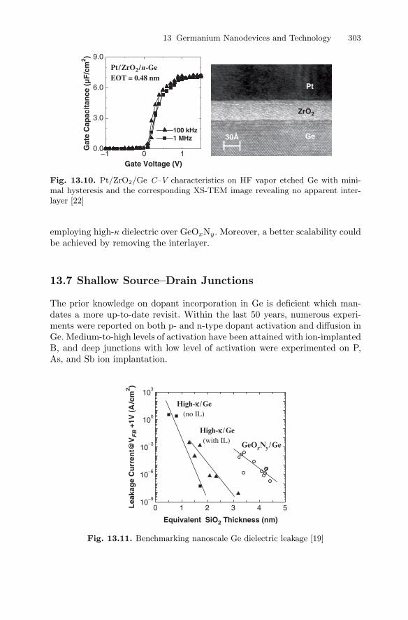
13 Germanium Nanodevices and Technology 303
−1 0 10.0
3.0
6.0
9.0
EOT = 0.48 nmPt/ZrO2/n-Ge
Gat
e C
apac
itan
ce (
µF
/cm
2 )
Gate Voltage (V)
100 kHz1 MHz
Pt
ZrO2
Ge30Å
Fig. 13.10. Pt/ZrO2/Ge C–V characteristics on HF vapor etched Ge with mini-mal hysteresis and the corresponding XS-TEM image revealing no apparent inter-layer [22]
employing high-κ dielectric over GeOxNy. Moreover, a better scalability couldbe achieved by removing the interlayer.
13.7 Shallow Source–Drain Junctions
The prior knowledge on dopant incorporation in Ge is deficient which man-dates a more up-to-date revisit. Within the last 50 years, numerous experi-ments were reported on both p- and n-type dopant activation and diffusion inGe. Medium-to-high levels of activation have been attained with ion-implantedB, and deep junctions with low level of activation were experimented on P,As, and Sb ion implantation.
0 1 2 3 4 510
−9
10−6
10−3
100
103
High-k /Ge(no IL)
GeOxNy/Ge
High-k /Ge(with IL)
Lea
kag
e C
urr
ent@
VF
B+1
V (
A/c
m2 )
Equivalent SiO2 Thickness (nm)
Fig. 13.11. Benchmarking nanoscale Ge dielectric leakage [19]

304 C.O. Chui, K.C. Saraswat
0 50 100 150 20010
16
1018
1020
1022
B (p-type)
SIMS - as-implantedSIMS - 650ºC, 10secSRP - 650ºC, 10sec
Co
nce
ntr
atio
n (
cm−3
)
Depth (nm)
0 50 100 150 20010
16
1018
1020
1022
P (n-type)
SIMS - as-implantedSIMS - 650ºC, 10secSRP - 650ºC, 10sec
Depth (nm)
Co
ncen
tration
(cm−3)
Fig. 13.12. SIMS (chemical) and SRP (electrically active) concentrations of ion-implanted B and P in Ge [23]. 49BF+
2 and 31P+ ions were implanted at 20 and18 keV, respectively, at a dose of 4 × 1015 cm−2
13.7.1 Ion Implantation Doping
Conventional ion implantation doping of various ionic species was carried outat a fixed dose and energies corresponding to a similar projected range [23].Symmetrically high levels of activation on both p- and n-type dopants in Gewere demonstrated at concentration directly applicable to advanced CMOS(Fig. 13.12). However, the fast n-type dopant diffusion was hindering any shal-low junction formation (Fig. 13.13).
0 100 200 300 400 500 600
1020
1019
1018
1017
1016
1015
Sb
AsAs
PP
Sb
650ºC
60 sec675ºC
5 sec
Ele
ctri
cal C
on
cen
trat
ion
(cm
-3)
Depth (nm)
Fig. 13.13. SRP profiles of various n-type dopants in Ge [23]

13 Germanium Nanodevices and Technology 305
13.7.2 Solid Source Diffusion Doping
As an alternative doping strategy, SSD is free from problems such as incom-plete dopant activation, channeling effects, transient enhanced diffusion, andextended defect formation even at very low energies. Besides these advantages,shallow junctions with low sheet resistance have been achieved in silicon us-ing SSD. In an attempt to obtain shallow junctions in Ge via diffusion fromheavily doped phospho-silicate glass (PSG), we have studied the SSD dop-ing in Ge [10]. PSG was deposited by low pressure chemical vapor deposition(LPCVD) in a hot wall furnace from a mixture of SiH4 and PH3 at 400C.Rapid thermal processing (RTP) was utilized to maximize the activation levelof the out-diffused dopants and minimize their redistribution.
The thermal anneal budget range of interest is highlighted in Fig. 13.14.For the 8 wt.% PSG that we used in our experiment, no appreciable out-diffusion was observed below 800C, which could be attributed to the lowdiffusivity of P inside the PSG layer at such low temperatures. The represen-tative spreading resistance probe (SRP) depth profiles after RTA at 850Care displayed in Fig. 13.15. These resultant n+/p junctions always showedthe peak concentration of about 1 × 1019 cm−3 at the surface. This high-est achievable peak concentration depends on several factors including theP concentration and diffusivity within the PSG layer, the P segregation atthe PSG/Ge interface, as well as the P solid solubility limit in Ge. As arule of thumb, in order to simultaneously lower the out-diffusion temper-ature and raise the surface peak concentration, a solid source with eitherhigher dopant concentration or diffusivity could be employed. Owing to theabsence of other extrinsic diffusion mechanisms, we extracted the intrinsicdopant diffusivity and plotted as a function of temperature (omitted here)that indicated a very good match with the published P diffusion coefficients[24] in Ge.
1017
1018
1019
1020
Pea
k C
on
cen
trat
ion
(cm
-3)
0
200
400
600
800
1000
10s900ºC
60s850ºC
20s850ºC
300s800ºC
8 wt% PSG on Ge
100s800ºC
Jun
ction
Dep
th (n
m)
Thermal Budget
Fig. 13.14. Peak electrically active concentration and junction depths obtained bySSD from 8wt.% PSG under different thermal anneal budgets [10]

306 C.O. Chui, K.C. Saraswat
0 300 600 900 120010
17
1018
1019
1020
P in Ge
850ºC, 20 sec850ºC, 60 sec
Ele
ctri
cal C
on
cen
trat
ion
(cm
-3)
Depth(nm)
Fig. 13.15. SRP profiles of out-diffused P [10]
13.8 Metal-Gated Germanium MOSFET Processes
Since the p-type dopant in Ge could be activated at a temperature as lowas 400C [25], the demand for a gate-last process for p-MOSFET fabricationis relatively low. The much higher activation temperature for n-type dopantsconversely mandates a low thermal budget self-aligned gate-last n-MOSFETprocess. However, an employment of the advanced replacement gate or dam-ascene gate process for Ge MOSFET fabrication is not always practical inmany situations.
13.8.1 The Sub-400C Conventional P-MOSFET Process
Since a standard device isolation technology has yet to be established to fabri-cate Ge MOSFETs in an integrated fashion, adopting a self-isolated transistorstructure would certainly help to expedite the technology evaluation process.A simple ring MOSFET structure was therefore chosen whose self-isolation isachieved by tying the source ring potential to ground.
The sub-400C process [25] began with the (100) oriented n-type Gewafers. Either a DI water rinsing or HF vapor etching was used in an attemptto remove native oxides, followed by the deposition of 4–5 nm ZrO2 using theultraviolet-assisted ozone oxidation. No threshold adjustment implant wasused. After the Pt gate electrode formation, a self-aligned source/drain BF+
2
implant was done. Dopant activation was then performed at 400C in N2 for30 min. Source/drain contact hole (ZrO2) etching and contact metallizationwere combined into a single lithography step. ZrO2 was first etched in chlorineplasma. While keeping the same photoresist masking, a Ti/Al metal stack was

13 Germanium Nanodevices and Technology 307
0.2 0.3 0.4 0.5 0.60
100
200
300
400
Si hi-k pFET
25µm Ge hi-k pFET (HFV)25µm Ge hi-k pFET (DIW)30µm Ge hi-k pFET (DIW)100µm Ge hi-k pFET (DIW)
Si UniversalMobility
Eff
ecti
ve M
ob
ility
(cm
2/V
-s)
Effective Field (MV/cm)
Fig. 13.16. Effective hole mobility vs. effective E-field extracted from Pt/ZrO2/Gep-MOSFETs with either DI water rinsing or HF vapor etching surface treatment [25]
e-beam evaporated followed by the liftoff process. Finally, the samples weresubjected to forming gas anneal at 300C for 30 min.
Ge p-MOSFETs with drawn channel length of 2–200 µm were all working.The shorter channel length devices exhibited relatively high IDsat but alsohigh off-state leakage, which composed primarily of the gate leakage at sucha low EOT. To minimize any error introduced by the gate leakage to theintrinsic IDsat measurements for accurate effective mobility extraction, thesePt/ZrO2/Ge p-MOSFETs were operated at gate and drain biases where thegate leakage was negligibly small. Effective hole mobility from these deviceswith different Ge surface cleaning are plotted in Fig. 13.16.
Since the effective hole mobility extracted from a limited number of devicesexhibited a slight distribution, no gate length dependence and no single prefer-ential Ge surface cleaning could be identified. In any case, these Pt/ZrO2/Gep-MOSFETs revealed roughly twofold enhancement in hole mobility over thesilicon universal mobility model and about three times higher mobility thanthat of high-κ/Si p-MOSFETs, both at low E-field. With proper optimizationof the device structure and fabrication process, it should be possible to at-tain even higher effective mobility and lower leakage. For instance, thin gatespacers together with source and drain extensions could be employed to bringthe metal contacts much closer to the channel to minimize parasitic resis-tances. Recently, variants of this high-κ on Ge concept had been subsequentlydemonstrated in Ge p-MOSFETs by other groups [26, 27] showing similarresults.
13.8.2 The Simple Self-Aligned Gate-Last n-MOSFET Process
In integrating novel channel materials like Ge, it is crucial and beneficial todevelop a simple low thermal budget process that is compatible with the Simainline equipment. Among other key criteria, standard field isolation to-gether with planar geometry is the foremost important. Embracing these two

308 C.O. Chui, K.C. Saraswat
• Channel region screen oxidation to prevent auto-doping
• S/D formation by PSG out-diffusion using RTP
• RTN in NH3 at 600˚C
• Conformal ALD of high-κ dielectric
Metal gate formed byphotoresist liftoff
• LTO deposited as the BEOL isolation ILD
• Contact hole etching (including LTO, PSG, & high-κ)
• Contact metallization
(c)
(d)
(e)
(a)
• LTO/PSG deposition
• S/D definition using dry (90%) + wet (10%) oxide etching
• Field isolation (RTN + LTO)
P-Well
P-Well
Ge Substrate
Ge Substrate
FOX
PSGLTO
PSGLTO
PSGLTO
PSGLTO
PSGLTO
PSGLTO
PSGLTO
PSGLTO
FOX
FOX FOX
P-Well
Ge Substrate
FOX FOX
P-Well
Ge Substrate
FOX
Metal MetalILDILD
FOX
P-Well
Ge Substrate
FOX FOX
• Screen oxidation
• P-Well implant
(b)
•
Fig. 13.17. The simple self-aligned gate-last Ge n-MOSFET process flow [10]
features, a simple self-aligned gate-last process has been developed [10] asdepicted in Fig. 13.17.
The starting substrates were very lightly doped (100) oriented p-type Gewafers. The field isolation was done by RTN at 600C followed by LPCVDSiO2 (LTO) deposition. After the active areas were opened, a screen oxide onthe Ge surface was thermally grown followed by p-well implant (Fig. 13.17a).An LTO-capped 8 wt.% PSG layer was then deposited. The source/drain re-gions were defined by a combinational etching of the LTO/PSG stack abovethe channel position (Fig. 13.17b). To further prevent auto-doping from the ex-posed PSG sidewalls, another screen oxide was grown on the channel surface

13 Germanium Nanodevices and Technology 309
0.0 0.5 1.00
2
4
6
8
Drain Voltage (V)
Pt/HfO2/GeOxNy/Ge
W/L= 2 µm/2 µmVGS= 0 to 1.5 V
So
urce C
urren
t (µA
/m)
0.0 0.5 1.00
2
4
6
8Pt/ZrO2/GeOxNy/Ge
W/L= 1.5 µm/ 1 µmVGS= 0 to 1.5 V
So
urc
e C
urr
ent
(µA
/µm
)
Drain Voltage (V)
Fig. 13.18. Output characteristics of Pt-gated Ge n-MOSFETs with either ZrO2
or HfO2 dielectrics [10]
prior to the source/drain formation by out-diffusion from PSG using RTP(Fig. 13.17c). The RTP was carried out at 850C for 10 s to achieve an ex-pected junction depth of about 0.28 µm. An RTN of the Ge channel was thenperformed at 600C followed by an ALD of ZrO2 or HfO2 of about 3 nm. Metalgate electrodes overlapping the source/drain were defined by photoresist liftoff(Fig. 13.17d). This gate-last process was completed by an LTO deposition forback-end-of-line isolation, contact hole etching, and metallization using 1%Si-doped Al (Fig. 13.17e). With the exception of the high-κ ALD step, thistailored five-lithography level process was launched in the mainline Si StanfordNanofabrication Facility (SNF).
Proof-of-concept Pt-gated Ge n-MOSFETs with either ZrO2 or HfO2 gatedielectric were fabricated using this self-aligned gate-last process. The ex-tracted inversion EOT (∼2.2 nm) is similar to the accumulation EOT ob-tained from simple MOS capacitors with an identical dielectric stack [21]. Thefeasibility of this simple process on novel channels has been confirmed withfunctional Ge n-MOSFETs with channel length down to 1–2 µm (Fig. 13.18).The non-linearity of the output characteristics at low drain voltage indicatedthe presence of a Schottky source/drain contact, which could be explained byeither the poor Pt electrode edge adhesion and/or the loss of ohmicity dueto deactivation of the out-diffused dopants during the interfacial RTN step.These issues could simple be solved by adapting a metal that sticks betterand a lower thermal budget GeOxNy synthesis.
Introduction of this simple self-aligned gate-last MOSFET process largelyrelaxes the stringent thermal stability requirement on novel gate stacks andchannels during dopant activation, while serving the same purpose as themore-involved replacement gate or damascene gate process. In addition, highselectivity etchings of (a) the metal gate electrode vs. the high-κ dielectric and(b) the high-κ dielectric vs. the channel are no longer essential in the presenceof the thick LTO/PSG buffer stack underneath as depicted in Fig. 13.17d.

310 C.O. Chui, K.C. Saraswat
Fig. 13.19. Extension of the novel process to fabricate complementary channelMOSFETs [10]
Fig. 13.20. Elevated source and drain junctions could be employed upon the re-placement of the insulating solid dopant source with a doped Si1−xGex alloy [10]
Many useful device structures could also be derived by extending thisversatile process. For example, complementary channel MOSFETs could berealized by selectively removing the PSG layer from the p-MOSFET areasfollowed by blanket deposition of a LTO capped borosilicate glass (BSG)film (Fig. 13.19). The complementary junctions for both p- and n-MOSFETare thus readily formed with a single RTP out-diffusion step. Moreover,heavily-doped poly-SixGe1−x alloys could be employed instead of insulat-ing doped glasses as the solid source. The resultant device structure wouldautomatically contain the doped SixGe1−x layer as the benign elevatedsource/drain junctions (Fig. 13.20), which however might require a high selec-tivity etching of the heavily-doped poly-SixGe1−x alloy vs. the lightly-dopedchannel.
13.9 Conclusions
Innovative device structures and new materials must be considered to con-tinue the historic progress in information processing and transmission. As apromising MOSFET channel material candidate, Ge offers numerous advan-tages over Si. In this chapter, we have first pointed out the technologicaldifficulties in the realization of Ge MOSFETs with classical problems such asthe lack of a sufficiently stable gate dielectric and prior knowledge on dopingGe. We have then reviewed various advanced Ge MOS technologies developedto tackle these issues including:

13 Germanium Nanodevices and Technology 311
(1) Nanoscale gate stacks with either grown germanium oxynitride or de-posited high-κ dielectrics,
(2) Shallow source/drain junctions by either ion implantation doping or solidsource diffusion doping, and
(3) Metal-gated Ge MOSFET processes using either a sub-400C conventionalp-MOSFET flow or a simple self-aligned gate-last n-MOSFET flow.
Utilizing these technologies, a sub-1 nm EOT gate stack, shallow source/drain Ge junctions, and functional metal-gated Ge MOSFETs with high-κdielectric have been demonstrated for the first time.
Acknowledgments
This work was supported by the DARPA HGI Program, the MARCO Mate-rials Structures and Devices Focus Center, and the Intel Foundation PhDFellowship. The authors would also like to acknowledge Ammar Nayfeh,Dr. Hyoungsub Kim, Dr. David Chi, Dr. Kailash Gopalakrishnan, Dr. Ro-hit Shenoy, Dr. Yonehara Takao, Dr. James P. McVittie, Prof. Paul C.McIntyre, Dr. Baylor B. Triplett, Dr. Peter B. Griffin, Prof. James D.Plummer, and Prof. Yoshio Nishi for their helps and discussions.
References
1. The International Technology Roadmap for Semiconductors, Semiconductor In-dustry Association, 2004 Update. (http://public.itrs.net/)
2. E.J. Nowak, “Maintaining the benefits of CMOS scaling when scaling bogsdown,” IBM J. Res. & Dev., vol. 46, pp. 169–180, 2002
3. M. Lundstrom, “Elementary scattering theory of the Si MOSFET,” IEEE Elec-tron Device Lett., vol. 18, pp. 361–363, 1997
4. M. Lundstrom and Z. Ren, “Essential physics of carrier transport in nanoscaleMOSFETs,” IEEE Trans. Electron Dev., vol. 49, pp. 133–141, 2002
5. A. Lochtefeld and D.A. Antoniadis, “On experimental determination of carriervelocity in deeply scaled NMOS: how close to the thermal limit?” IEEE ElectronDev. Lett., vol. 22, pp. 95–97, 2001
6. S. Takagi, “Re-examination of subband structure engineering in ultra-shortchannel MOSFETs under ballistic carrier transport,” VLSI Symp. Tech. Dig.,pp. 115–116, 2003
7. Electronic Archive of New Semiconductor Materials, Characteristics and Prop-erties, Ioffe Physico-Technical Institute. (http://www.ioffe.rssi.ru/SVA/NSM/Semicond/)
8. R. Chau, S. Datta, M. Doczy, B. Doyle, B. Jin, J. Kavalieros, A. Majum-dar, M. Metz, and M. Radosavljevic, “Benchmarking nanotechnology for high-performance and lower-power logic transistor applications,” IEEE Trans. Nan-otech., vol. 4, pp. 153–158, 2005

312 C.O. Chui, K.C. Saraswat
9. C.O. Chui, A.K. Okyay, and K.C. Saraswat, “Effective dark current suppres-sion with asymmetric MSM photodetectors in Group IV semiconductors,” IEEEPhoton. Technol. Lett., vol. 15, pp. 1585–1587, 2003
10. C.O. Chui, H. Kim, P.C. McIntyre, and K.C. Saraswat, “A germanium NMOS-FET process integrating metal gate and improved hi-k dielectrics,” IEEE IEDMTech. Digest, pp. 437–440, 2003
11. J.C. Bean, T.T. Sheng, L.C. Feldman, A.T. Fiory, and R. T. Lynch, “Pseud-morphic growth of GexSi1−x on silicon by molecular beam epitaxy,” Appl. Phys.Lett., vol. 44, pp. 102–104, 1984
12. D.J. Eaglesham and M. Cerullo, “Low-temperature growth of Ge on Si(100),”Appl. Phys. Lett., vol. 58, pp. 2276–2278, 1991
13. M.T. Currie, S.B. Samavedam, T.A. Langdo, C.W. Leitz, and E.A. Fitzgerald,“Controlling threading dislocation densities in Ge on Si using graded SiGe layersand chemical-mechanical polishing,” Appl. Phys. Lett., vol. 72, pp. 1718–1720,1998
14. Hsin-Chiao Luan, D.R. Lim, K.K. Lee, K.M. Chen, J.G. Sandland, K. Wada, andL.C. Kimerling, “High-quality Ge epilayers on Si with low threading-dislocationdensities,” Appl. Phys. Lett., vol. 75, pp. 2909–2911, 1999
15. A. Nayfeh, C.O. Chui, K.C. Saraswat, and T. Yonehara, “Effects of hydrogenannealing on heteroepitaxial-Ge layers on Si: Surface roughness and electricalquality,” Appl. Phys. Lett., vol. 85, pp. 2815–2817, 2004
16. A. Nayfeh, C.O. Chui, T. Yonehara, and K.C. Saraswat, “Fabrication of high-quality p-MOSFET in Ge grown heteroepitaxially on Si,” IEEE Electron DeviceLett., vol. 26, pp. 311–313, 2005
17. N. Sato and T. Yonehara, “Hydrogen annealed silicon-on-insulator,” Appl. Phys.Lett., vol. 65, pp. 1924–1926, 1994
18. D.J. Hymes and J.J. Rosenberg, “Growth and materials characterization of na-tive germanium oxynitride thin films on germanium,” J. Electrochem. Soc., vol.135, pp. 961–965, 1988
19. C.O. Chui, F. Ito, and K.C. Saraswat, “Scalability and electrical propertiesof germanium oxynitride MOS dielectrics,” IEEE Electron Dev. Lett., vol. 25,pp. 613–615, 2004
20. C.O. Chui, D.-I. Lee, A.A. Singh, P.A. Pianetta, and K. C. Saraswat, “Zirconia-germanium interface photo-emission spectroscopy using synchrotron radiation,”J. Appl. Phys., vol. 97, p. 113518, 2005
21. C.O. Chui, H. Kim, P.C. McIntyre, and K.C. Saraswat, “Atomic layer depo-sition of high-k dielectric for germanium MOS applications: substrate surfacepreparation,” IEEE Electron Dev. Lett., vol. 25, 2004
22. C.O. Chui, S. Ramanathan, B.B. Triplett, P.C. McIntyre, and K. C. Saraswat,“Germanium MOS capacitors incorporating ultrathin high-k gate dielectric,”IEEE Electron Dev. Lett., vol. 23, pp. 473–475, 2002
23. C.O. Chui, K. Gopalakrishnan, P.B. Griffin, J.D. Plummer, and K.C. Saraswat,“Activation and diffusion studies of ion-implanted p- and n-dopants in germa-nium,” Appl. Phys. Lett., vol. 83, 2003
24. W.C. Dunlap, Jr., “Diffusion of impurities in germanium,” Phys. Rev., vol. 94,pp. 1531–1540, 1954
25. C.O. Chui, H. Kim, D. Chi, B.B. Triplett, P.C. McIntyre, and K.C. Saraswat,“A sub-400C germanium MOSFET technology with high-k dielectric and metalgate,” IEEE IEDM Tech. Digest, pp. 437–440, 2002

13 Germanium Nanodevices and Technology 313
26. C.H. Huang, M.Y. Yang, A. Chin, W.J. Chen, C.X. Zhu, B. J. Cho, M.-F.Li, D.L. Kwong, “Very low defects and high performance Ge-on-insulator p-MOSFETs with Al2O3 gate dielectrics,” VLSI Symp. Tech. Dig., pp. 119–120,2003
27. A. Ritenour, S. Yu, M.L. Lee, N. Lu, W. Bai, A. Pitera, E. A. Fitzgerald, D.L.Kwong, and D.A. Antoniadis, “Epitaxial strained germanium p-MOSFETs withHfO2 gate dielectrics and TaN gate electrode,” IEEE IEDM Tech. Digest, pp.433–436, 2003
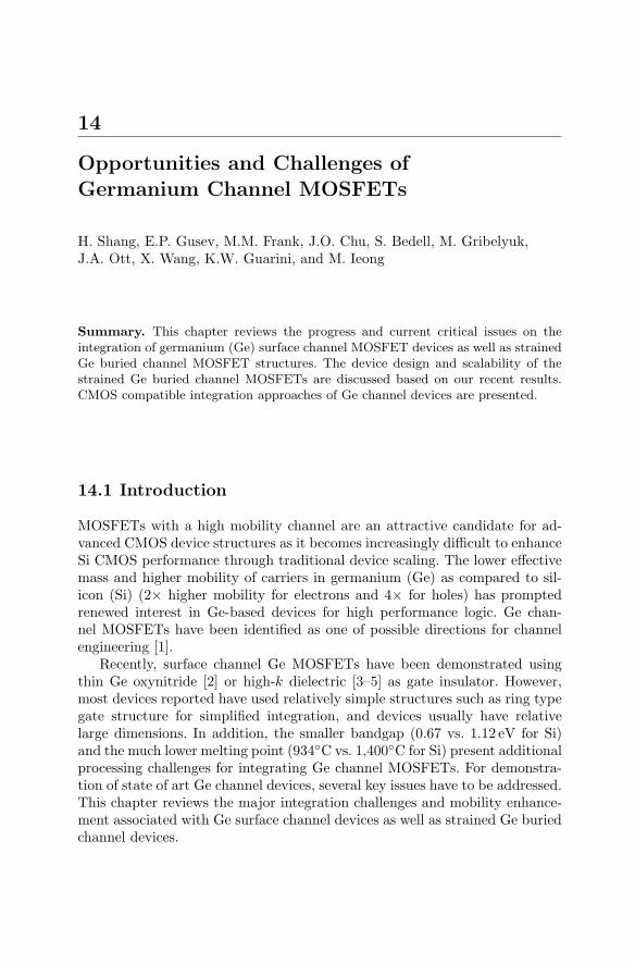
14
Opportunities and Challenges ofGermanium Channel MOSFETs
H. Shang, E.P. Gusev, M.M. Frank, J.O. Chu, S. Bedell, M. Gribelyuk,J.A. Ott, X. Wang, K.W. Guarini, and M. Ieong
Summary. This chapter reviews the progress and current critical issues on theintegration of germanium (Ge) surface channel MOSFET devices as well as strainedGe buried channel MOSFET structures. The device design and scalability of thestrained Ge buried channel MOSFETs are discussed based on our recent results.CMOS compatible integration approaches of Ge channel devices are presented.
14.1 Introduction
MOSFETs with a high mobility channel are an attractive candidate for ad-vanced CMOS device structures as it becomes increasingly difficult to enhanceSi CMOS performance through traditional device scaling. The lower effectivemass and higher mobility of carriers in germanium (Ge) as compared to sil-icon (Si) (2× higher mobility for electrons and 4× for holes) has promptedrenewed interest in Ge-based devices for high performance logic. Ge chan-nel MOSFETs have been identified as one of possible directions for channelengineering [1].
Recently, surface channel Ge MOSFETs have been demonstrated usingthin Ge oxynitride [2] or high-k dielectric [3–5] as gate insulator. However,most devices reported have used relatively simple structures such as ring typegate structure for simplified integration, and devices usually have relativelarge dimensions. In addition, the smaller bandgap (0.67 vs. 1.12 eV for Si)and the much lower melting point (934C vs. 1,400C for Si) present additionalprocessing challenges for integrating Ge channel MOSFETs. For demonstra-tion of state of art Ge channel devices, several key issues have to be addressed.This chapter reviews the major integration challenges and mobility enhance-ment associated with Ge surface channel devices as well as strained Ge buriedchannel devices.

316 H. Shang et al.
14.2 Ge Surface Channel MOSFETs
14.2.1 Gate Dielectric
One major roadblock for Ge CMOS device fabrication is that it is very difficultto obtain a stable gate dielectric. A water-soluble native Ge oxide that istypically present on the upper surface of a Ge-containing material causes theinstability of the gate dielectric.
The best-known native dielectric candidate on Ge is Ge oxynitride(GeOxNy). High quality, thin GeOxNy can be formed on Germanium by nitri-dation of a thermal grown germanium oxide. Rapid thermal oxidation (RTO)at 500–600C followed by a rapid thermal nitridation at 600–650C in am-monia (NH3) ambient is generally been practiced. NH3 is chosen as nitridingagent due to its greater ability to incorporate more nitrogen into the oxyni-tride film over other species like nitrous oxide (N2O) and nitric oxide (NO).Using this method, the resulting film thickness can be scaled down as thinas EOT of 1.9 nm with acceptable leakage and the refractive index is foundabout 1.3–1.5 [6]. Comparing with native Ge oxides (GeO and GeO2), it hasthe improved thermal and chemical stability [7, 8]. In addition, the incorpo-ration of nitrogen into Ge oxides could suppress any potential interdiffusionbetween the gate dielectric and substrate and/or the gate electrode. High per-formance Ge MOSFETs with enhanced mobility over Si MOSFETs with SiO2
were demonstrated using a relative thick GeON (EOT ∼5 nm) [2,9]. However,the most important application for high quality thin GeOxNy is perhaps thatit could serve as a stable interlayer for integration of novel high-k dielectricsinto Ge MOS devices.
The recent developments of high-quality deposition techniques, such asatomic layer deposition (ALD) and metal-organic chemical vapor deposition(MOCVD), to deposit dielectric films with high dielectric constants (on the or-der of about 4.0 or greater, typically about 7.0 or greater) for the replacementof SiO2 in Si MOSFETs has prompted activities to develop Ge MOSFETsimplementing such dielectrics. Binary metal oxides (e.g., ZrO2, HfO2) havebeen the primary choices as a high-k gate dielectric. In addition, germinate(MeGexOy), where Me stands for a metal with high ion polarazibility, e.g.,Hf, Zr, La, Y, Ta, Ti, etc., are also proposed to potentially improve the carriermobility and the interface stability.
14.2.2 Ge Surface Preparation
One of most challenging tasks for Ge/high-k MOS systems is the Ge surfacepreparation and interface control before high-k film deposition.
For Ge, specifically, it appears essential to have a surface free of germaniumoxide before high-k film deposition. A conventional solution for Si has been touse (concentrated or dilute) hydrofluoric acid (e.g., HF or DHF) to remove anynative Si oxide, while leaving an H-passivated surface. Despite being successful

14 Opportunities and Challenges of Ge Channel MOSFETs 317
for Si CMOS device fabrication, this surface passivation technique was foundto be less effective on Ge [10].
One demonstrated method to fabricate functional gate stacks is to desorbthe Ge oxide in an ultra-high vacuum (UHV) system at high temperatures(360 to 650C) followed by in situ high-k deposition [11–13]. In fact, crys-talline oxides such as CeO2 [14] and BaTiO3 [15] have been successfully grownon Ge(100) using this method in conjunction with pulsed laser deposition andmolecular beam epitaxy. The main drawback of this approach is that UHVsystems are costly and generally incompatible with standard ALD or MOCVDhigh-k deposition tools used in manufacturing. A practical solution is basedon nitridation of a wet-etched (e.g., using DHF) Ge surface prior to dielectricdeposition using either atomic N exposure or a high-temperature NH3 gastreatment [5, 16–18].
We found both the microstructure of the high-k film deposited on Ge andthe electrical property of Ge/high-k MOS capacitors are very sensitive to theGe surface preparation prior to high-k film deposition [17]. In our experiment,Ge surface is first wet cleaned, and then HfO2 is deposited on Ge substrate byALCVD. It is interesting that HfO2 grows epitaxially on the wet cleaned Gesurface with DI H2O last process, while amphorous HfO2 is observed on theGe surface treated with nitrogen passivation by RT NH3 process (at 650Cfor 1 min), as shown in Fig. 14.1. Figure 14.2 shows the C–V characteristics ofMOS capacitors for both cases. In contrast to the large frequency dispersionobserved in the DI water last sample, very little frequency dispersion showedfor the sample with nitrogen passivation. The large dispersion is probably dueto the Ge and Hf interdiffusion at the Ge–HfO2 interface, which might havebeen effectively reduced in the case of nitrogen passivation by RT NH3 beforeHfO2 deposition. However hysteresis still remains and additional traps arealso introduced during the RTNH3 process. The nitridation step also inducesfixed positive charge at the interface which causes a large negative flatbandshift and could degrade the device mobility.
Several research groups have recently reported that effective passivationcan be achieved by using SiH4 [19]. EOT as thin as 7.5 A was reported withplasma PH3 treatment and thin AlN layer [20] combined with HfO2/TaNgate stack. Besides the above-mentioned physical passivation methods, novelwet chemistries are also being studied to passivate Ge surface during pre-clean. Chlorine-passivated [21] and sulfur-passivated [22] Ge surfaces are twoexamples.
Although much progress has been made on this subject, more deep under-standing and well controlled Ge surface is needed for successful application ofhigh-k dielectric on Ge MOS devices.
14.2.3 Dopant Diffusion and Junction Leakage
Compared to bulk Si, boron diffusion is suppressed while As diffusion is en-hanced in SiGe and Ge (Fig. 14.3) [23]. This will favor the formation of ultra

318 H. Shang et al.
Al
HfO2
Ge
Fig. 14.1. High resolution TEM images of HfO2 deposited on (a) wet cleaned Gesurface with DI H2O last process; (b) RT NH3 treated Ge surface after wet clean.Crystalline HfO is observed on case (a)
shallow junctions in P channel Ge MOSFETs, while presenting a challengefor N channel Ge MOSFETs. Methods such as co-implantation have beendemonstrated to show that As diffusion in 20–75% SiGe can be reduced 2.5–3.7× [23].
The smaller bandgap in Ge has been a concern for its influence on junctionleakage and band-to-band tunneling. To investigate the junction leakage asso-ciated with the smaller bandgap in Ge, both P+/N and N+/P Ge diodes aremade by boron and phosphorous implantation. The junction leakage of bothN+/P and P+/N Ge diodes can be reduced to ∼10−4 Acm−2 with annealing,as shown in Fig. 14.4. This is considered acceptable for device operation.
On extremely scaled MOSFETs, band-to-band tunneling is a great concern[24]. The band-to-band tunneling current increases exponentially in smallerbandgap semiconductors, thus could be a more serious issue for Ge MOSFETs.Detailed study of its impact on Ge MOSFET scaling can be found in [25].

14 Opportunities and Challenges of Ge Channel MOSFETs 319
UM Ge water last
DI water last then NH3/650C/1min
Gate Bias(V)
Cap
acit
ance
(F
)C
apac
itan
ce (
F)
12x10−10
1.0x10⁻¹⁰
8.0x10⁻¹¹
6.0x10⁻¹¹
4.0x10⁻¹¹
2.0x10⁻¹¹
0.0
12x10−10
1.0x10⁻¹⁰
8.0x10⁻¹¹
6.0x10⁻¹¹
4.0x10⁻¹¹
2.0x10⁻¹¹
0.0
−2 −1 0 1
Gate Bias(V)
−2 −1 0 1
100K1Mhz10KHz
100Kz1Mhz10KHz
Fig. 14.2. The C–V characteristics of Ge/HfO2/Al MOS capacitors (a) Ge waswet cleaned only, (b) Ge was wet cleaned, then treated with RT NH3. The fre-quency dispersion is significantly reduced in (b), possibly due to the reduced Ge–Hfinterdiffusion at the interface
14.3 Strained Ge Buried Channel MOSFETs
By adding a high quality thin layer of Si on top of Ge, good quality of Si/SiO2
interface can be achieved. In addition, Si based gate dielectric and high-κ filmscan be applied on the devices. Combined with strained Ge (s-Ge) channelgrown on top of relaxed SiGe, the s-Ge buried channel devices are expectedto have improved mobility due to the very small effective hole mass (0.1m0)in s-Ge layer and the reduced surface roughness scattering. Indeed, dramatichole mobility enhancement of 4–25× has been demonstrated in s-Ge MOS-FETs [26–30] – the highest mobility enhancement for hole carriers among allavailable options. On the other hand, one of the major concerns for buriedchannel devices has been the device scalability.

320 H. Shang et al.
Fig. 14.3. B and As diffusion coefficient in Ge (600C) compared to 75% SiGe andSi (1,000C) S–Ge could benefit from a reduced As diffusion by co-implantation
14.3.1 Device Design and Scaling Prospect for StrainedGe Buried Channel Devices
It is known that the effective gate dielectric in buried channel devices is in-creased comparing with surface channel operation, resulting in worse shortchannel effects, such as larger subthreshold swing and Vt rolloff. Thus the s-Ge buried channel device must be carefully designed and evaluated to ensuregreater performance without short channel degradation [30].
To achieve maximum performance in the s-Ge buried channel MOSFETs,most carriers must be confined within the high mobility s-Ge layer. We
Fig. 14.4. Reverse junction leakage in Ge as a function of anneal temperature. Withanneal, both P + /N and N + /P junction leakage can be reduced to ∼10−4 A cm−2

14 Opportunities and Challenges of Ge Channel MOSFETs 321
Fig. 14.5. Energy band offset, layer structure, and retrograde doping profile of s-GeBC PMOSFETs used in electro-static simulation
performed 1-D electro-static simulations to determine the upper limit of theSi cap thickness whereby 90% of the total on-state carriers would be confinedin the s-Ge layer. Fig. 14.5 shows the device layer structure along with theband offset used in this simulation. A valence band offset of 450 meV betweenthe s-Ge and the Si cap is assumed [31]. Fig. 14.6a shows the ratio of carriersin the buried s-Ge layer over the total carriers at the on-state as a functionof Si cap thickness. The strong dependence of carrier confinement on the Sicap thickness is clearly shown for heavily doped channel structures. When achannel doping of 1× 1019 cm−3 is employed, the Si cap thickness must be atmost 1.5 nm in order to keep >90% of carriers in the buried Ge channel. 2-Dsimulations are also performed to investigate the scalability of sub-100 nm s-Ge BC PMOSFETs with an Si cap of 1.5 nm. Fig. 14.6b shows Vt roll-off andDIBL of s-Ge BC PMOSFETs as compared to the Si surface channel controldevice. With a retrograde doping profile of 1016 and 5×1018 cm−3. s-Ge buriedchannel PMOSFETs exhibit similar short channel characteristics as bulk SiSC devices [30].
14.3.2 Material Growth and Thermal Stability
There are two main techniques to obtain a strained Ge or high Ge content SiGelayer: chemical vapor deposition (CVD) or Ge condensation (also called ther-mal mixing [29]). Both ultra-high vacuum (UHV) CVD and PECVD methodshave been reported for s-Ge growth [26,27,30].
In our experiment, the s-Ge BC structure is grown using the low tempera-ture UHV-CVD technique with the Si cap thickness down to 1 nm. The growthof the s-Ge BC structure begins with a relaxed ∼75% SiGe buffer followed byan s-Ge channel (13 nm) and an ultra-thin Si cap (1.5 nm). TEM (Fig. 14.7)shows the high quality and atomic abruptness for both the Si cap/Ge andGe/SiGe interfaces. AFM results (RMS = 6.7 nm) show a relatively smoothsurface, which can be further improved by applying an intermediate CMP topolish the SiGe buffer layer [23, 24]. Triple axis X-ray diffraction measure-ments were used to quantify the strain in the Ge channel and the Ge content

322 H. Shang et al.
1
200
175
150
125
100
75
50
25
020 40 60 80
0
Tox=1nmTGe=10nm
Buried ChannelSurface Channel
20
40
60
80
100
120
140
160
2 3
1
0.8
0.6
0.4
rati
o=N
bc
/No
nD
IBL
(m
V)
dVtl
in (
mV
)
Channel Length Lg (nm)
0.2
0
Tsi (nm)
4
1e16cm-3
1e18cm-3
1e19cm-3
5
Fig. 14.6. (a) The ratio of carriers in buried Ge channel over the total carriers atNon = 1e13 cm−2 as a function of Si cap thickness for three channel dopings. (b) Vt
roll-off and DIBL of s-Ge BC PMOSFETs as compared to the Si SC control with aretrograde doping profile of 1016 and 5×1018 cm−3 as shown in Fig 14.5
and strain relaxation of SiGe buffer layer. Strain relaxation during the devicefabrication is a big concern. We measured the strain of the s-Ge channel afterfurnace anneals at temperatures from 550C to 700C for 30 min. As shownin Fig. 14.8, virtually no strain relaxation is observed after annealing up to600C, but there is significant relaxation at 650C and above. This will setthe upper limit of the s-Ge device processing temperatures. For an RTA-basedanneal, the strain relaxation is found similar trend as furnace anneal results.
14.3.3 Gate Stack for s-Ge MOSFETs
Achieving a high quality thin gate dielectric for s-Ge MOSFETs is provenchallenging as well. As shown above, to maintain the strain in the s-Ge chan-nel, all processing temperatures should be kept below 600C to prevent strainrelaxation [27]. Because of this constraint, low temperature deposited high-kdielectric and Si dioxide (LTO) had been used as the gate dielectric of s-GeMOSFETs [26–29].

14 Opportunities and Challenges of Ge Channel MOSFETs 323
Fig. 14.7. XTEM of a s-Ge on 75% SiGe grown by UHVCVD. Both s-Ge and thinSi cap layers are uniform and smooth
We have developed a new low temperature (400C) remote plasma ox-ide as the gate dielectric for UHVCVD grown s-Ge channel MOSFETs. Thistechnique enables us to achieve the thinnest high quality Si oxide ever re-ported on Ge. Fig. 14.9a shows the typical C–V characteristics of MOS ca-pacitors with EOT = ∼3 nm remote plasma oxide on Si. Figure 14.9b showsthe interface trap density measured using the conductance method, whereDit is found ∼2.5×1010 cm−2-eV, very close to that measure on MOS ca-pacitors with ∼3 nm thermal SiO2. Similar leakage current is found on theremote plasma oxide MOS capacitors on both Si and UHV s-Ge samples.The high quality low temperature remote plasma oxide is essential for achiev-ing high performance s-Ge channel PMOSFETs with thin SiO2 as the gatedielectric.
14.3.4 Integration of s-Ge Channel MOSFETs
Although much work have been done to demonstrate great hole mobilityenhancement in s-Ge channel PMOSFETs using simple structures to avoid
Fig. 14.8. Strain relaxation after furnace anneals at 550C to 700C for 30min. Nosignificant strain relaxation is found when T <= 600C

324 H. Shang et al.
Remote Plasma Oxide
remote Plasma SiO2
EOT=34.5A
1.2
1.0
0.8
0.6
0.4
0.2
0.0−4 −3 −2 −1 0
thermal SiO2
5
4
3
2
1
Dit=2
5*G
/w(X
1010
/cm
2 -eV
)
0−0.8 −0.6 −0.4 −0.2
VG(V)
VG(V)
C(m
F/c
m2 )
1 2
Fig. 14.9. (a) Typical C–V characteristics of Si MOS capacitor with the remoteplasma oxide formed at 400C. With this technique, as thin as 2.5 nm SiO2 can beachieved on s-Ge buried channel for high performance PMOSFETs demonstration.(b) The interface trap density is measured using the high frequency conductancetechnique. Dit of Si MOS capacitor with remote plasma oxide is found comparableto that with thermal SiO2
complicate processing issues, a compatible process to incorporate s-Ge struc-tures into standard CMOS technology is needed. One of the proposed idealCMOS structure is shown in Fig. 14.10, where PMOSFETs employ a burieds-Ge channel while NMOSFETs employ an Si or strained Si surface chan-nel. This structure requires to form a thin s-Ge channel selectively only onPMOSFET regions [32].
In our work, we use SGOI substrates with ∼30% Ge as the starting ma-terial. A standard STI process is performed to form SGOI active regions.An optional patterning step could be used to mask the NMOSFET regionswith oxide or nitride. Two techniques can be used to form an s-Ge channelselectively on the patterned SGOI regions using:

14 Opportunities and Challenges of Ge Channel MOSFETs 325
Fig. 14.10. Schematic cross section of a proposed ideal CMOS structure forthe maximum enhancement of both hole and electron mobility. The Ge channelin the pFET regions can be formed by selective Ge growth or deposition by maskingthe NFET region with oxide or nitride film
(1) Local thermal mixing (LTM). High-temperature oxidation to enrich theGe content in the SGOI layer – “TM Ge”, or
(2) Selective UHVCVD process. Growth of an s-Ge layer with a thin Si capusing UHVCVD – “UHV Ge”
In the “TM Ge” sample, Ge fraction is found ∼67% with 1.47% compres-sive strain as measured by XRD analysis. In addition, medium energy ionscattering (MEIS) analysis shows the Ge content in the SGOI layer after lo-cal thermal mixing is ∼60%. For the “UHV Ge” sample, cross section TEMimages (Fig. 14.11) confirmed the selectivity of the s-Ge layer growth, suchthat s-Ge is formed only on top of the SiGe and not on the STI regions(oxide).
Fig. 14.11. TEM image of selective s-Ge layer grown by UHVCVD method, whereGe is only grown on top of SGOI, while no Ge growth is found on top of STIregions

326 H. Shang et al.
Table 14.1. Two types of the fabricated strained Ge/SiGe PMOSFETs selectivelyformed by UHVCVD and thermal mixing techniques respectively
Ge channel Ge% in Si cap Gate oxideDevice formation channel (nm) (nm)
“TM Ge” Thermal mixing 60 none 6.5 nm HfO2
“UHV Ge” UHVCVD 100 5a 2.5 nm SiO2
a as-grown
After forming the s-Ge layer, a conventional CMOS process is used fordevice fabrication, including gate stack formation, S/D implants, and metalcontacts. For both “UHV Ge” and “TM Ge” device fabrication, we use insitu boron doped poly-Si as the gate electrode. Table 14.1 lists the physicalparameters of the two types of fabricated Ge channel MOSFETs.
“TM Ge” with HfO2 Gate Oxide
For “TM Ge” MOSFETs, the surface is first treated using RT NH3, then∼6.5 nm HfO2 is deposited by MOCVD at 500C as the gate dielectric.Figure 14.12 is the TEM image of the “TM Ge” device showing the HfO2
gate dielectric under the polysilicon gate.Figure 14.13a, b shows the linear current and transconductance character-
istics of the “TM Ge” PMOSFETs with HfO2 gate oxide, along with the Sicontrol. The channel length of both devices are 10 µm. Approximately 2.5×performance enhancement is observed in both linear and saturation regimes.Figure 14.14 shows the subthreshold characteristics of the “TM Ge” PMOS-FETs with HfO2 gate oxide along with the Si control. The subthreshold
Fig. 14.12. TEM image of the fabricated PFETs with s-SiGe channel using thermalmixing method The gate oxide is ∼65 nm HfO2 deposited using MOCVD method

14 Opportunities and Challenges of Ge Channel MOSFETs 327
L=10µm, VDS=50mV
Si/HiO2control
TMs-Ge/HiO2
L=10µm, VDS=50mVSi/HiO2control
TMs-Ge/HiO2
1×10⁻⁵
8×10⁻⁶
6×10⁻⁶
4×10⁻⁶
2×10⁻⁶
0−3.0 −25 −20 −1.5
VGS(V)
2.5X
2.5X
I DS (
A/s
qu
are)
VGS(V)
I DS (
A/s
qu
are)
−1.0 −0.5 −0.0 −0.5
8
7
6
5
4
3
2
1
0−3 −2 −1 0
Fig. 14.13. Linear current (a) and transconductance (b) characteristics of thefabricated PMOSFETs with HfO2 gate oxide on 60% SiGe channel formed by localthermal mixing, comparing with Si channel PMOSFETs control with HfO2
slope is ∼125mV dec−1 in “TM Ge”, ∼98mV dec−1 in the Si control. Thethreshold voltage in the linear region Vtlin is extracted using the constantcurrent at 70 nA square−1. We found that the Vtlin in the Si/HfO2/poly-Sicontrol is ∼ − 0.67V. In contrast, the Vtlin from the “TM Ge” device isfound ∼−0.36V, which is ∼300mV lowered from that in the Si/HfO2/poly-Sicontrol.
One of the most important issues in Si/HfO2/poly-Si PMOSFETs to-day is the high Vth due to the Fermi level pinning [33]. Because of the va-lence band offset, the Ge channel allows the Vth of HfO2/poly Si PMOS-FETs to be lowered to the appropriate Vth for high performance CMOStechnology.
VGS(V)
I DS (
A/s
qu
are)
L=10µm
Si/HiO2 controlTMs-Ge/HiO2
VDS=50mV,−1V
10−3
−3.0−2.5−2.0−1.5−1.0−0.5 0.0 0.5
10−4
10−5
10−6
10−7
10−8
10−9
10−10
10−11
Fig. 14.14. Subthreshold characteristics of PMOSFETs with HfO2 gate oxide on60% SiGe channel formed by local thermal mixing, comparing with Si channelPMOSFETs control with HfO2
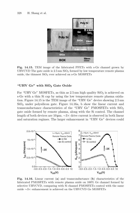
328 H. Shang et al.
Fig. 14.15. TEM image of the fabricated PFETs with s-Ge channel grown byUHVCVD The gate oxide is 2.5 nm SiO2 formed by low temperature remote plasmaoxide, the thinnest SiO2 ever achieved on s-Ge MOSFETs
“UHV Ge” with SiO2 Gate Oxide
For “UHV Ge” MOSFETs, as thin as 2.5 nm high quality SiO2 is achieved ons-Ge with a thin Si cap by using the low temperature remote plasma oxida-tion. Figure 14.15 is the TEM image of the “UHV Ge” device showing 2.5 nmSiO2 under polysilicon gate. Figure 14.16a, b show the linear current andtransconductance characteristics of the “UHV Ge” PMOSFETs with SiO2
gate oxide formed by remote plasma, along with the Si control. The channellength of both devices are 10 µm. ∼3× drive current is observed in both linearand saturation regimes. The larger enhancement in “UHV Ge” devices could
2.0×10⁻⁵
15×10−5
1.0×10⁻⁵
5.0×10⁻⁵
0.0−3.0−2.5−2.0−1.5
VGS(V) VGS(V)
I DS (
A/s
qu
are)
Gm
(mS
/sq
uar
e)
−1.0−0.5−0.0−0.5 10 −3.0−2.5−2.0−1.5−1.0−0.5−0.0−0.5 10
L=10µm, VDS=50mV
Remote Plasma Oxides-Ge
~3X ~3X
Si control
L=10µm, VDS=50mV
Remote Plasma Oxide
s-GeSi control
8
7
6
5
4
3
2
1
0
Fig. 14.16. Linear current (a) and transconductance (b) characteristics of thefabricated PMOSFETs with remote plasma oxide on 100% Ge channel formed byselective UHVCVD, comparing with Si channel PMOSFETs control with the sameoxide ∼3× enhancement is achieved on the UHVCVD Ge MOSFETs

14 Opportunities and Challenges of Ge Channel MOSFETs 329
10−3
10−4
10−5
10−6
10−7
10−8
10−9
10−10
10−11
VGS(V)−3.0 −2.5 −2.0 −1.5 −10 −0.5 0.0 0.5 1.0
I DS (
A/s
qu
are)
L=10µmremote plasma oxide
Si/ control (0.4/10)s-Ge(10/10)
VDS=50mV,−1V
Fig. 14.17. Substhreshold characteristics of PMOSFETs with remote plasma oxideon 100% Ge channel formed by selective UHVCVD
be due to the higher Ge content (100% vs. 60%) in the channel and a SiO2-based gate dielectric. On the other hand, higher subthreshold leakage currentis found on the “UHV Ge” PMOSFETs, as seen from the subthreshold char-acteristics in Fig. 14.17. This is probably due to the growth defects in the s-Gelayer and may be improved by process optimization.
It is worth to point out that in both “TM Ge” and “UHV Ge” devices,device performance enhancement over Si controls is demonstrated due to thesignificantly enhanced hole mobility.
14.4 Conclusions
Surface passivation and gate dielectric, dopant diffusion, and junction leak-age are the three most serious challenges of Ge CMOS devices. By using thes-Ge with an ultra thin Si cap, standard Si surface passivation and gate di-electric can be applied without significant modification. Table 14.2 comparess-Ge BC MOSFETs with Ge SC devices. S-Ge BC can be integrated with
Table 14.2. Comparison of s-Ge BC with Ge SC devices in critical processing issuesand mobility enhancements (+: positive; −: negative; =: equivalent)
Ge SC s-Ge BC
Gate stack − +Dopant diffusion − +Junction leakage = =Integration w. Si − +Electron mobility − +Hole mobility + ++

330 H. Shang et al.
fewer processing challenges, significantly higher hole mobility and improvedelectron mobility. These results indicate that the s-Ge BC MOSFET with anultra-thin Si cap is a promising option for future scaled CMOS devices. Weshow a CMOS-compatible integration scheme for s-Ge channel PMOSFETs,including the conventional STI isolation and scaled thin gate dielectrics forhigh performance CMOS technology. Although it is a major step towardsintegrating s-Ge channels into CMOS technology for continued performanceenhancements, much work remains to be done in the demonstration of state ofart short channel Ge PMOSFETs with sufficient performance enhancement.
Acknowledgements
The authors thank the IBM T.J. Watson Research MRL and CSS facilities fortheir help in device fabrication. In addition, we thank Dr. Shahidi Ghavam,Dr. T.C. Chen for managerial support. One of authors wish to thank Dr. H.-S.Philip Wong for valuable discussions and initial encouragement.
References
1. S. Takagi, T. Mizuno, T. Tezuka, N. Sugiyama, T. Numata, K. Usuda, Y.Moriyama, S. Nakaharai, J. Koga, A. Tanabe, N. Hirashita and T. Maeda,IEDM. Tech. Dig., p. 57, 2003.
2. H. Shang, H. Okorn-Schmidt, K.K. Chan, M. Copel, J.A. Ott, P. M. Kozlowski,S.E. Steen, S.A. Cordes, H.-S.P. Wong, E.C. Jones and W.E. Haensch, “Highmobility p-channel germanium MOSFETs with a thin Ge oxynitride gate di-electric”, in IEDM Tech. Dig., p. 441, 2002.
3. C.O. Chui, H. Kim, D. Chi, B. Triplett, P.C. McIntyre and K.C. Saraswat, “Asub-400C germanium MOSFET technology with high-k dielectric and metalgate”, in IEDM Tech. Dig., p. 437, 2002.
4. C.H. Huang, M.Y. Yang, A. Chin, W.J. Chen, C.X. Zhu, B.J. Cho, M.-F. Liand D.L. Kwong, ” Very low defects and high performance Ge-on-insulator p-MOSFET’s with Al2O3 gate dielectrics”, in VLSI Symp. Tech. Dig., pp. 119–120,2003.
5. W.P. Bai, N. Lu, J. Liu, A. Ramirez, D.L. Kwong, D. Wristers, A. Ritenour, L.Lee and D. Antoniadis, “Ge MOS characteristics with CVD HfO2 gate dielectricsand TaN gate electrode” in VLSI Symp. Tech. Dig. 2003, pp. 121–122.
6. C.O. Chui, F. Ito and K.C. Saraswat, “Scalability and Electrical properties ofGermanium oxynitride MOS dielectrics”, in IEEE Electron Device Lett., vol 25,no. 9 Sept. 2004.
7. O.J. Gregory, E.E. Crisman, L. Pruitt, D.J. Hymes and J.J. Rosenberg, “Elec-trical characterization of some native insulators on germanium” in Proc. Mater.Res. Soc. Symp., vol. 76 1987, pp.307–311.
8. D.J. Hymes and J.J. Rosenberg, “Growth and materials characterization of na-tive germanium oxynitride thin films on germanium”, J. Electrochem. Soc., vol.135, pp. 961–965, 1988.

14 Opportunities and Challenges of Ge Channel MOSFETs 331
9. H. Shang, H. Okorn-Schmidt, K.K. Chan, M. Copel, J.A. Ott, P. M. Kozlowski,S.E. Steen, S.A. Cordes, H.-S.P. Wong, E.C. Jones and W.E. Haensch et al.,“Electrical characterization of Germanium P-channel MOSFETs”, in IEEEElectron Device Lett., vol. 24, pp. 242–244, Apr. 2003.
10. D. Bodlaki et al. “Ambient stability of chemically passivated germanium inter-faces”, Surface Science 543, pp. 63–74, 2003.
11. X.-J. Zhang et al., “Thermal desorption of ultraviolet-ozone oxidized Ge (001)for substrate cleaning”, in J. Vac. Sci. Technol. A 11(5), Sep/Oct, p. 2553, 1993
12. J.J.-H. Chen, N. Bojarczuk, H. Shang, M. Copel, J. Hannon, J. Karasinski, E.Preisler, S.K. Banerjee and S. Guha, “Ultrathin Al2O3 and HfO2 gate dielectricon surface-nitrided Ge”, in IEEE Trans. Electron Dev. 51, p. 1441, 2004.
13. A. Dimoulas, G. Mavrou, G. Vellianitis, E. Evangelou, N. Boukos, M. Houssaand M. Caymax, “HfO2 high-k gate dielectrics on Ge (100) by atomic oxygenbeam deposition”, Appl. Phys. Lett. 86, 032908, 2005.
14. D.P. Norton, F.J. walker and M.F. Chisholm, Appl. Phys. Lett. 76, p. 1677,2000.
15. R.A. McKee, F.J. Walker and M.F. Chisholm, Science 293, p. 468, 2001.16. C.O. Chui, H. Kim, P. McIntyre and K.C. Saraswat, “Atomic layer deposition
of high-k dielectric for Germanium MOS applications–substrate surface prepa-ration”, in IEEE Electron Device Lett. 25, p. 274, 2004.
17. E.P. Gusev, H. Shang, M. copel, M. Gribelyuk, C. D’Emic, P. Kozlowski and T.Zabel, “Microstructure and thermal stability of HfO2 gate dielectric depositedon Ge (100)”, in Appl. Phys. Lett. 85, p. 2334, 2004.
18. N. Wu, .Q. Zhang, C. Zhu, D.S.H. Chan, M.F. Li, N. Balasubramanian, A.Chin and D.L. Kwong, et al., “Effect of surface NH3 anneal on the physical andelectrical properties of HfO2 films on Ge substrate”, in Appl. Phys. Lett. 84, p.3741, 2004.
19. N. Wu, Q. Zhang, C. Zhu, C. Yeo, S.J. Whang, D.S.H. Chan, M. F. Li, A.Chin, D.L. Kwong, A.Y. Du, C.H. Tung and N. Balasubramanian, “Alternativesurface passivation on germanium for metal-oxide-semiconductor applicationswith high-k gate dielectric”, in Appl. Phys. Lett., 85, p. 4127, 2004.
20. S.J. Whang, S.J. Lee, F. Gao, N. Wu, C.X. Zhu, J. Pan, L.J. Tang, D.L.Kwong, “Germanium p- & n-MOSFETs fabricated with novel surface passi-vation (plasma PH3 and thin AlN) and TaN/HfO2 gate stack” in IEDM Tech.Dig. 2004.
21. G.W. Anderson, M.C. Hanf, P.R. Norton, Z.H. Lu, and M.J. Graham, “TheS-passivation of Ge (100) – 1×1”, Appl. Phys. Lett. 9, p. 1123, 1995.
22. Z.H. Lu, “Air stable Cl-terminated Ge (111)”, in Appl. Phys. Lett. 68(4), 1996.23. K. Lee, F. Cardone, P. Saunders, P. Kozlowski, P. Ronsheim, H. Zhu, J. Li, J.
Chu; K. Chan, and M. Ieong, “20 nm N/sup +/ abrupt junction formation instrained Si/Si1−x/Gex/ MOS device”, in IEDM Tech. Dig., p. 481. 2003.
24. P. Solomon, D.J. Frank, J. Jopling, C. D’Emic, O. Dokumaci, P. Ronsheim,and W. Haensch, “Tunnel current measurements on P/N junction diodes andimplications for future device design”, in IEDM Tech. Dig. 2003.
25. T. Krishnamohan, Z. Krivokapic, K. Uchida, Y. Nishi, and K.C. Saraswat, “Lowdefect Ultra-thin Fully Strained-ge MOSFET on relaxed Si with high mobilityand low band-to-band tunneling”, in VLSI Symp. Tech. Dig., p. 82, 2005.
26. A. Ritenour, S. Yu, M.L. Lee, N. Lu, W. Bai, A. Pitera, E.A. Fitzgerald, D.L.Kwong, and D.A. Antoniadis, “Epitaxial strained germanium p-MOSFETs withHfO2 gate dielectric and TaN gate electrode”, in IEDM Tech. Dig., p. 433, 2003.

332 H. Shang et al.
27. M. Lee and E.A. Fitzgerald, “Optimized strained Si/strained Ge dual-channelheterostructures for high mobility p- and n-MOSFETs”, IEDM Tech. Dig., p.429, 2003.
28. T. Irisawa, S. Tokumitsu, T. Hattori, K. Nakagawa, S. Koh and Y.Shiraki, “Ultrahigh room-temperature hole Hall and effective mobility inSi0.3Ge0.7/Ge/Si0.3Ge0.7 heterostructures”, in Appl. Phys. Lett. 81, p. 847,2002.
29. T. Tezuka, S. Nakaharai, Y. Moriyama, N. Sugiyama and S. Takagi, “Selectively-formed high mobility SiGe-on-insulator pMOSFETs with Ge-rich strained sur-face channels using local condensation technique”, in VLSI Symp. Tech. Dig.,2004, p. 198, 2004.
30. H. Shang, J.O. Chu, X. Wang∗, P.M. Mooney, K. Lee, J. Ott, K. Rim, K.Chan, K. Guarini and M. Ieong, “Channel design and mobility enhancementin strained germanium buried channel MOSFETs”, in VLSI Symp. Tech. Dig.,2004, p. 204., 2004.
31. R. People, “Physics and applications of GexSi1-x/Si strained-layer heterostruc-tures”, in IEEE J. Quan. Elect, Vol. QE-22, p. 1696, 1986.
32. H. Shang, Jack O. Chu, S. Bedell, E.P. Gusev, P. Jamison∗, Y. Zhang, J.A. Ott,M. Copel, D. Sadana, K. W. Guarini, and M. Ieong, “Selectively formed highmobility strained Ge PMOSFETs for high performance CMOS”, in IEDM Tech.Dig., 2004.
33. C. Hobbs, L. Fonseca, V. Dhandapani, S. Samavedam, B. Taylor, J. Grant, L.Dip, D. Triyoso, R. Hegde, D. Gilmer, R. Garcia, D. Roan, L. lovejoy, R. Rai,L. Hebert, H. Tseng, B. White and P. Tobin, “Fermi level pinning at the polySi/metal oxide interface”, in VLSI Symp. Tech. Dig., 2003. p. 9, 2003.

15
Germanium Deep-Submicron p-FETand n-FET Devices, Fabricated onGermanium-On-Insulator Substrates
M. Meuris, B. De Jaeger, J. Van Steenbergen, R. Bonzom,M. Caymax, M. Houssa, B. Kaczer, F. Leys, K. Martens, K. Opsomer,A.M. Pourghaderi, A. Satta, E. Simoen, V. Terzieva, E. Van Moorhem,G. Winderickx, R. Loo, T. Clarysse, T. Conard, A. Delabie, D. Hellin,T. Janssens, B. Onsia, S. Sioncke, P.W. Mertens, J. Snow, S. Van Elshocht,W. Vandervorst, P. Zimmerman, D. Brunco, G. Raskin, F. Letertre,T. Akatsu, T. Billon, and M. Heyns
Summary. A key challenge in the engineering of Ge MOSFETs is to develop aproper Ge surface passivation technique prior to high-k dielectric deposition to ob-tain low interface state density and high carrier mobility. A review on some possibletreatments to passivate the Ge surface is discussed. Another important aspect isthe activation of p- and n-type dopants to form the active areas in devices. Fi-nally, Ge deep submicron n- and p-FET devices fabricated with this technique ongermanium-on-insulator substrates, yield promising device characteristics, showingthe feasibility of these substrates.
15.1 Introduction
The need for electron and hole mobility enhancement and the progress inthe development of high-k gate stacks, has lead to renewed interest in GeMOSFETs. However, before Ge devices can be used for advanced circuits,many issues of the Ge processing and device properties have to be addressed.In the first place, the mobility enhancement of Ge vs. Si, as observed in longchannel transistors, has to be proven to result in a larger drive current forshort channel transistors. Second, it must be possible to manufacture theseGe devices in a silicon-like semiconductor manufacturing environment. Lastbut not least, the reliability and yield of the Ge-based circuits, has to besufficient to allow ULSI circuits.
To study the feasibility of a Ge CMOS transistor technology, a short chan-nel transistor in bulk Ge was processed. A 200mm〈100〉 n-type bulk Ge waferswere used. The wafer specifications are similar to that of silicon wafers usedin ULSI processing. We designed a 3 masks process flow to fabricate the Gedevices, consisting only of silicon compatible process steps performed in a

334 M. Meuris et al.
0
50
100
150
200
−1 −0.8 −0.6 −0.4 −0.2 0
0.0V
−0.4V
−1.0V
−1.6V
−2.0V
I D [
µA/µ
m]
VD [V]
L = 0.18µm VG-VT
Fig. 15.1. At the left side an SEM picture of a 0.18 µm Ge pMOS transistor withfield isolation, dry etched metal gate and spacers. At the right side the correspondingtransistor characteristics
200 mm silicon prototyping line. Special care was taken to avoid the exposureof bare Ge surfaces to the aggressive wet processing steps, with the excep-tion of HF chemistry [1, 2]. A 10 nm HfO2 (200 ALD cycles) was used as agate dielectric. A detailed description of the processing can be found in [3].In Fig. 15.1, an SEM picture and the transistor characteristics is shown of apMOS transistor with 0.18 µm gate length. These results demonstrate thatthe processing of germanium in a silicon manufacturing line is possible.
In order to make Ge devices with a larger drive current than an Si device,a key challenge is to develop a proper Ge surface passivation technique toobtain low interface state density and high carrier mobility.
A second challenge to improve the device characteristics is the activationof n-type and p-type dopants with minimal diffusion. To obtain sub-45 nmdevices, low resistance in very shallow (10–20 nm) source and drain regions isa key parameter.
And another concern is the type of wafer, which will be used for the sub-45 nm devices. It is foreseen that Si technology will make use of fully depleteddevices, most probably “finfet” or “3-gate” type of structures. In order toprocess these devices, SOI is necessary. Therefore if Ge is used in scaled CMOSdevices, GeOI (germanium on insulator) wafers will be mandatory.
In this paper, these three issues are addressed.
15.2 Ge Gate Stack Capacitor
For the passivation of the capacitor gate stack on Ge several options have beenproposed in the literature. Treatments with NH3 anneal [4, 5], SiH4 anneal[6] or plasma treatment in PH3 [7] were used with mixed success. Also the
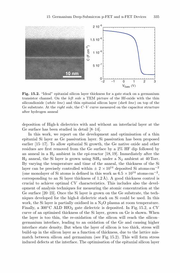
15 Germanium Deep-Submicron p-FET and n-FET Devices 335
0
5 10−7
1 10−6
1.5 10−6
2 10−6
−2 −1 0 1 2 3
C (
F.c
m−2
)VGate (V)
Fig. 15.2. “Ideal” epitaxial silicon layer thickness for a gate stack on a germaniumtransistor channel. On the left side a TEM picture of the Hf-oxide with the thinsilicondioxide (white line) and thin epitaxial silicon layer (dark line) on top of theGe substrate. At the right side, the C–V curve measured on the capacitor structureafter hydrogen anneal
deposition of High-k dielectrics with and without an interfacial layer at theGe surface has been studied in detail [8–14].
In this work, we report on the development and optimisation of a thinepitaxial Si layer as Ge passivation layer. Si passivation has been proposedearlier [15–17]. To allow epitaxial Si growth, the Ge native oxide and otherresidues are first removed from the Ge surface by a 2% HF dip followed byan anneal in a H2 ambient in the epi-reactor [18, 19]. Immediately after theH2 anneal, the Si layer is grown using SiH4 under a N2 ambient at 40 Torr.By varying the temperature and time of the anneal, the thickness of the Silayer can be precisely controlled within ± 2 × 10¹⁴ deposited Si atoms cm−2
(one monolayer of Si atoms is defined in this work as 6.5 × 10¹⁴ atoms cm−2,corresponding to an Si layer thickness of 1.2 A). A good thickness control iscrucial to achieve optimal CV characteristics. This includes also the devel-opment of analysis techniques for measuring the atomic concentration at theGe surface [20–23]. Once the Si layer is grown on the Ge substrate, the tech-niques developed for the high-k dielectric stack on Si could be used. In thiswork, the Si layer is partially oxidised in a N2O plasma at room temperature.Finally, a 300C ALD HfO2 gate dielectric is deposited. In Fig. 15.2, a CVcurve of an optimised thickness of the Si layer, grown on Ge is shown. Whenthe layer is too thin, the re-oxidation of the silicon will reach the silicon–germanium interface, leading to an oxidation of the Ge and causing higherinterface state density. But when the layer of silicon is too thick, stress willbuild-up in the silicon layer as a function of thickness, due to the lattice mis-match between silicon and germanium (see Fig. 15.2). This will form stressinduced defects at the interface. The optimisation of the epitaxial silicon layer

336 M. Meuris et al.
Table 15.1. Transistor channel mobility values of different passivation techniquesfor the Ge gate stack: the Si epitaxial layer [10], the NH3 anneal [3] and PH3 anneal[5]
p-FET n-FET
µeff (cm2 V−1 s−1) EOT (A) µeff (cm2 V−1 s−1) EOT (A)
Si [10] 170 26 10 26NH3 [3] 210 16 ∼0.2 ?PH3 [5] 125 17? 300 17?
thickness and its influence on the capacitor properties is extensively describedin [24].
The importance of the passivation of the germanium/high-k dielectric in-terface was further demonstrated in [25], where the problem of making annMOS on germanium was explained by the presence of a high interface statedensity near the conduction band of germanium. We explained that this isprobably due to a specific oxidation state of the Ge bond at the interface. Us-ing the Si passivation technique, decent channel mobility values were obtainedas well for nMOS as for pMOS devices as shown in Table 15.1.
15.3 Dopant Activation in Germanium
For making a short channel transistor device, very shallow and high conductivep- and n-type active area regions are essential. Therefore high doping (i.e.,activation) with low diffusion of the p- and n-type dopant species is necessary.In [26] it is described that boron as a p-type species can be activated atrelative low temperatures and without a measurable diffusion. However, then-type species as P and As show high diffusion coefficients at the activationtemperature for the dopant concentrations of interest in nano-electronics.
In [27,28] a more optimal implant and anneal condition for boron as a p-type species in germanium is described. The boron is easier to activate when apre-amorphization with Ge is done before the boron implantation. A completere-crystallization of the Ge amorphous layer can be obtained at temperaturesas low as 400C.
An extensive study [29, 30] of P in Ge as the n-type dopant species re-vealed that for phosphor three distinct concentration regions exist, with verydifferent behaviour. When P is implanted above 2 × 10²⁰ P at. cm−3, a largeout diffusion towards the germanium surface together with a pile-up near theprojected range of the implanted phosphor (attributed to the formation of Pclusters) is observed. When P is implanted in the region between 2×10¹⁹ and2× 1020 P at. cm−3, a large diffusion of P into the bulk of the Ge is observedwith SIMS measurements, showing a concentration dependent diffusion of P inGe. Implantations below 2×10¹⁹ P at. cm−3, result in no measurable diffusion
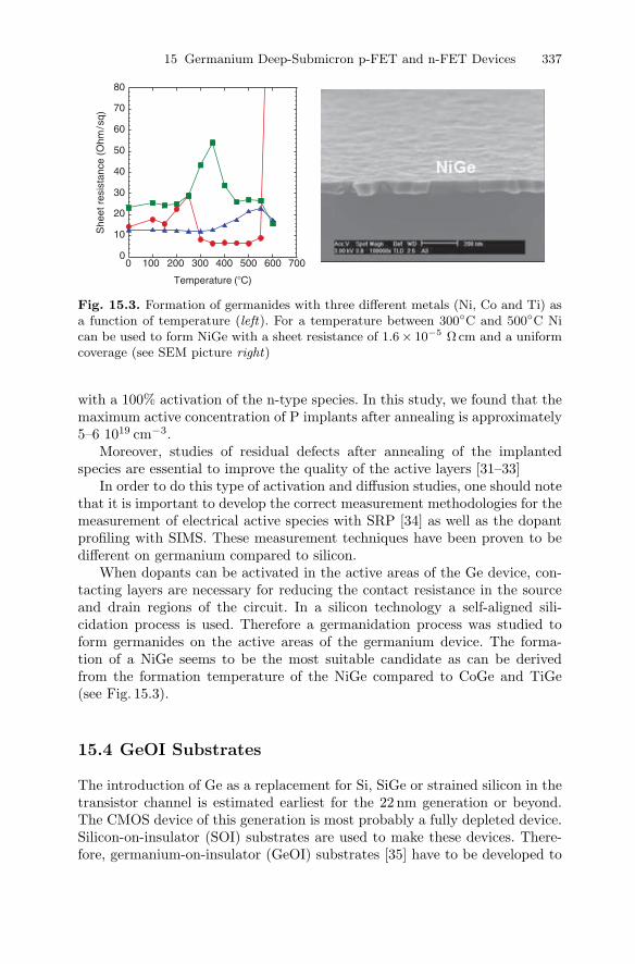
15 Germanium Deep-Submicron p-FET and n-FET Devices 337
0
10
20
30
40
50
60
70
80
0 100 200 300 400 500 600 700
She
et r
esis
tanc
e (O
hm/s
q)
Temperature (C)
Fig. 15.3. Formation of germanides with three different metals (Ni, Co and Ti) asa function of temperature (left). For a temperature between 300C and 500C Nican be used to form NiGe with a sheet resistance of 1.6× 10⁻⁵ Ωcm and a uniformcoverage (see SEM picture right)
with a 100% activation of the n-type species. In this study, we found that themaximum active concentration of P implants after annealing is approximately5–6 1019 cm−3.
Moreover, studies of residual defects after annealing of the implantedspecies are essential to improve the quality of the active layers [31–33]
In order to do this type of activation and diffusion studies, one should notethat it is important to develop the correct measurement methodologies for themeasurement of electrical active species with SRP [34] as well as the dopantprofiling with SIMS. These measurement techniques have been proven to bedifferent on germanium compared to silicon.
When dopants can be activated in the active areas of the Ge device, con-tacting layers are necessary for reducing the contact resistance in the sourceand drain regions of the circuit. In a silicon technology a self-aligned sili-cidation process is used. Therefore a germanidation process was studied toform germanides on the active areas of the germanium device. The forma-tion of a NiGe seems to be the most suitable candidate as can be derivedfrom the formation temperature of the NiGe compared to CoGe and TiGe(see Fig. 15.3).
15.4 GeOI Substrates
The introduction of Ge as a replacement for Si, SiGe or strained silicon in thetransistor channel is estimated earliest for the 22 nm generation or beyond.The CMOS device of this generation is most probably a fully depleted device.Silicon-on-insulator (SOI) substrates are used to make these devices. There-fore, germanium-on-insulator (GeOI) substrates [35] have to be developed to

338 M. Meuris et al.
0
20
40
60
80
100
0 1 2 3 4
I sou
rce(
µA/µ
m)
Vgate [V]
W = 2µm
0.5 µm 0.15 µm0.18 µm
0
100
200
300
400
500
600
700
−2 −1 0 1
L=0.5 µm L=0.25 µm L=0.18 µmI s
ourc
e(µA
/µm
)
Vgate [V]
W = 2µm
Fig. 15.4. pMOS (left) and nMOS (right) transistor characteristics of devices fabri-cated on a GeOI substrate. The excellent properties show the feasibility of the GeOIsubstrate technology
enable the possibility of making similar devices in Ge. To provide insight inthe quality of the Ge layer of GeOI substrates, transistor devices ere madein such GeOI substrates. Ge-on-insulator (GeOI) wafers from collaborationbetween SOITEC, UMICORE, LETI and IMEC were used, with a 200 nmthick Ge layer [21,36]. The gate dielectric is 10 nm HfO2 and the metal gate isa 10 nm PVD TaN/70 nm PVD TiN stack. In Fig. 15.4, the pMOS and nMOSdevice characteristics are shown. These devices, which are made in the Getop layer of the GeOI wafers, are of similar quality and performance as theones made on Ge bulk wafers. This demonstrates the feasibility of the GeOItechnology and the well-known result that the performance of Ge devices islargely dominated by the passivation process of the HiK/Ge interface.
15.5 Conclusions
An overview of the different technologies to be developed for a Ge CMOSdevice technology has been given. The major obstacle is the development of aGe gate stack with a low amount of interface states at the germanium/high-kdielectric interface. Also high dopant activation and low diffusion of p-type andn-type species have to be improved. In order to make Ge a viable technologyfor CMOS scaling, a high quality Ge on insulator substrate is necessary.
Acknowledgements
The support of the Core Partners of imec (Infineon, Intel Corp., Matsushita,Philips, Samsung, ST, Texas Instruments and TSMC) is highly acknowledged.
The support of the PLINE is acknowledged for the difficulty in processingthe Ge bulk substrates.

15 Germanium Deep-Submicron p-FET and n-FET Devices 339
Funding from FWO research project G.0273.05 is acknowledged.Funding from the EU under the ET4US contract is acknowledged.
References
1. B. Onsia et al., On the application of a thin ozone based wet chemical oxide asan interface for ALD high-k deposition, 7th International Symposium on UltraClean Process of Silicon Surfaces, 2005.
2. B. Onsia et al., A study of the influence of typical wet chemical treatmentson the germanium wafer surface, 7th International Symposium On Ultra CleanProcess of Silicon Surfaces, 2005.
3. B. De Jaeger et al., Ge deep sub-micron pFETs with etched TaN metal gateon a high-k dielectric, fabricated in a 200 mm silicon prototyping line, in: Proc.ESSDERC, 2004, pp. 189–192.
4. W.P. Bai et al., Ge MOS characteristics with CVD HfO2 gate dielectrics andTaN gate electrode, in: Proc. of the Symposium on VLSI technology, 2003, pp.121–122.
5. A. Ritenour et al., Epitaxial Strained Germanium p-MOSFETs with HfO2 GateDielectric and TaN Gate Electrode, in: Proc. IEDM, 2003, pp. 433–436.
6. N. Wu et al., Alternative surface passivation on germanium for metal-oxide-semiconductor applications with high-k gate dielectric, Appl. Phys. Lett., 85,2004, pp. 4127–4129.
7. S.J. Whang et al., Germanium p- and n-MOSFETs fabricated with novel surfacepassivation (plasma-PH3 and thin AlN) and HfO2/TaN Gate Stack, in: Proc.IEDM, 2004, pp. 307–310.
8. S. Van Elshocht et al., “Physical characterization of HfO2 deposited on Gesubstrates by MOCVD”, MRS Spring Meeting - High-k Insulators and Ferro-Electrics for Advanced Microelectronics Devices, D5.4, 2004.
9. M. Houssa et al., Electrical characteristics of Ge/GeOx(N)/HfO2 gate stacks,J. Non-Cryst. Solids, 2004.
10. S. Van Elshocht et al., Deposition of HfO2 on germanium and the impact ofsurface pretreatments, Appl. Phys. Lett., 2004, 3824.
11. S. Van Elshocht, et al. “Surface preparation techniques for high-k depositionon Ge substrates,” Proceedings of 7th International Symposium on Ultra CleanProcessing of Silicon Surfaces – UCPSS, Brussels, Belgium, Solid State Phenom.,103–104, 2004, 31.
12. A. Delabie et al., Atomic layer deposition of hafnium oxide on germanium sub-strates, J. Appl. Phys., 97, 064104 (2005).
13. Meuris et al., The future of high-k on pure germanium and its importance forGe CMOS, Mater. Sci. Semiconductor Process., 2005, p. 203.
14. S. Van Elshocht, et al., Study of CVD high-k gate oxides on high-mobilityGe and Ge/Si substrates, Thin Solid Films, 508, 2006 pp. 1–5, Proceedings ofthe Fourth International Conference on Silicon Epitaxy and Heterostructures(ICSI-4).
15. L.C. Kimerling and H-C Luan, US patent 6,352,942 (2002).
16. N.E. Posthuma et al., Surface passivation for germanium photovoltaic cells’Solar Energy Mater. Solar Cells, 88(1), 2005, 37.
17. Wu et al., Appl. Phys. Lett., 2004.
340 M. Meuris et al.
18. R. Bonzom et al., Growth Kinetics and Relaxation Mechanism of Very ThinEpitaxial Si films on (100) Germanium, presented at 2005 Spring Meeting ofthe MRS (2005).
19. F.E. Leys et al., Epitaxy solutions for Ge MOS technology, Thin Solid Films508, 2006, pp. 292–296, Proceedings of the Fourth International Conference onSilicon Epitaxy and Heterostructures (ICSI-4).
20. D. Hellin et al., ‘Determination of metallic contaminants on Ge wafers us-ing direct- and droplet sandwich etch – total reflection X-ray fluorescencespectrometry’, Spectrochim. Acta Part B 58, 2003, 2093–2104.
21. D. Hellin et al., ‘Vapor phase decomposition – droplet collection – totalreflection X-ray fluorescence spectrometry for metallic contamination analysisof Ge wafers’, Spectrochim. Acta Part B 60, 2005, 209–213.
22. D. Hellin et al., Total reflection X-ray fluorescence spectrometry for theintroduction of novel materials in clean-room production environments, IEEETrans. on Device Mater. Reliab., 5, 2005, pp. 639–651.
23. D. Hellin et al., ‘VPD-DC-TXRF for metallic contamination analysis of Gewafers’, Proceedings of the 7th International Symposium on Ultra CleanProcess of Silicon Surfaces (UCPSS 2004), 2005.
24. B. De Jaeger et al., INFOS, 2005.25. Croon et al., Proceedings of the International Conference on Microelectronic
Test Structures of 2004, 2005, p. 191.26. Chui et al., Appl. Phys. Lett., 83, 2003, 3276.27. A. Satta et al., Diffusion, activation and re-crystallization of boron implanted in
pre-amorphized and crystalline germanium, Appl. Phys. Lett., 87, 2005, 172109.28. A. Satta et al., Dopants for N and P junctions in Germanium, Proceedings of
ECS Spring Symposium 2005, 2005, p. 468.29. A. Satta et al., P implantation doping of Ge: Diffusion, activation, and
recrystallization, J. Vac. Sc. Technol. B 24, 2006, pp. 494–498.30. A. Satta et al., P implantation on doping of Ge: diffusion, activation, re-
crystallization, The 8th Int. Workshop on the Fabrication, Characterizationand Modeling of Ultra Shallow Junctions in Semiconductors, 2005.
31. E. Simoen et al., Defect removal, dopant diffusion and activation issues inion-implanted shallow junctions fabricated in crystalline germanium sub-strates, GADEST 2005(Gettering And Defect Engineering in SemiconductorTechnology) Conference 2005.
32. A. Satta et al., Ion implantation in Ge and the associated defect control, ECSDECON, 2005.
33. A. Satta et al., Shallow junction ion implantation in Ge and associated defectcontrol, J. Electrochem. Soc., 153, 2006, pp. G229–G233.
34. T. Clarysse et al., Active dopant characterization methodology for Germanium,USJ – The 8th International Workshop on the Fabrication, Characterizationand Modeling of Ultra Shallow Junctions in Semiconductors, 2005.
35. C. Deguet et al., From 100 mm to 200mm Germanium-On-Insulator (GeOI)structures realised by the smart cutTM technology, in: Proceedings of the FirstEUROSOI Workshop, pp. 31–33 2005.
36. T. Akatsu et al., 200mm Germanium-on-insulator(GeOI) by Smart Cuttechnology and recent GeOI MOSFETs achievements, IEEE International SOIConference, 2005.

16
Processing and Characterization of III–VCompound Semiconductor MOSFETs UsingAtomic Layer Deposited Gate Dielectrics
P.D. Ye, G.D. Wilk, and M.M. Frank
Summary. We demonstrate III–V compound semiconductor (GaAs, InGaAs, andGaN) based metal-oxide-semiconductor field-effect transistors (MOSFETs) withexcellent performance using an Al2O3 high-permittivity (high-k) gate dielectric,deposited by atomic layer deposition (ALD). These MOSFET devices exhibit ex-tremely low gate-leakage current, high transconductance, high dielectric breakdownstrength, a high short-circuit current-gain cut-off frequency (fT) and maximum os-cillation frequency (fMAX), as well as high output power and power added efficiency.ALD is a robust process that enables repeatability and manufacturability for com-pound semiconductor MOSFETs. In order to contribute to the fundamental un-derstanding of ALD-grown high-k/III–V gate stack quality, we discuss stack andinterface formation mechanisms in detail for Al2O3 and HfO2 gate dielectrics onGaAs.
16.1 Introduction
GaAs-based metal-oxide semiconductor field-effect transistors (MOSFETs)have been a subject of study for several decades [1–18]. GaAs-based de-vices potentially have great advantages over Si-based devices for high-speedand high-power applications, in part from an electron mobility in GaAsthat is ∼5× greater than that in Si, the availability of semi-insulatingGaAs substrates, and a higher breakdown field compared to Si. Currently,the GaAs metal-semiconductor field-effect-transistor (MESFET) or high-electron-mobility-transistor (HEMT) is the dominant device for high-speedand microwave-circuits. MESFETs or HEMTs feature gates formed by de-positing metal directly on the semiconductor, forming metal-semiconductor(Schottky-barrier) junctions, while MOSFETs have oxide layers (higher bar-rier) between the metal gate and the semiconductor channel. Compared toGaAs MESFETs or HEMTs, GaAs MOSFETs feature a larger maximumdrain current, much lower gate leakage current, a better noise margin, andmuch greater flexibility in digital IC design due to large gate voltage range.

342 P.D. Ye et al.
The main obstacle to GaAs-based MOSFET devices has been the lack ofhigh-quality, thermodynamically stable insulators on GaAs as the gate dielec-tric that can match device criteria similar to SiO2 on Si. Both GaAs-basednative oxides and deposited insulating layers have been attempted as gate di-electrics. For native oxidation of GaAs, various approaches were applied, i.e.,wet oxidation, plasma oxidation, laser-assisted oxidation, vacuum ultravio-let photochemical oxidation, etc. These approaches have had limited successat the device level, however, mainly due to instability of the native oxides ofGaAs, and due to the unacceptably high interface trap density Dit nearly uni-versally observed with native and deposited oxides. Such interface defects giverise to Fermi level pinning. For example, Fermi level pinning upon GaAs oxida-tion has been attributed to oxygen-induced displacement of surface As atoms,where doubly O-coordinated second-layer Ga atoms give rise to gap states [19].Excess interfacial As occupying AsGa antisite defects causes gap states as well[19,20]. Interfacial As may be formed via decomposition of As2O3 in the vicin-ity of GaAs, resulting from the reaction: As2O3 +2GaAs → Ga2O3 +4As [21].After decades of efforts on forming a deposited amorphous oxide on a III–V compound semiconductor using PECVD with decent interface quality [2],much progress has been made recently using in situ deposited Ga2O3(Gd2O3)or Ga2O3 and Gd2O3 dielectrics using ultrahigh-vacuum multi-chamber mole-cular beam epitaxy (MBE) [22–28] and ex situ atomic layer deposition (ALD)grown Al2O3 on III–V semiconductors [29–35]. Both methods have been shownto provide a high-quality interface with a low Dit on GaAs. Fermi level unpin-ning in the Ga2O3/GaAs system is achieved through a Ga2O/GaAs-like inter-face in which the Ga and As surface atoms are restored to near-bulk charge,preventing gap state formation [19]. Promising results have been demonstratedin GaAs MOSFETs using these techniques. Processing and properties of MBE-grown Ga2O3(Gd2O3) gate dielectrics are addressed in detail in Chap. 3.4 byKwo. Herein, we focus on ALD Al2O3. Another issue for GaAs circuits incompetition with silicon is the large defect densities which also preclude largescale integration. The emerging strategy is to use III–V compound semicon-ductors as NMOS conduction channels and Ge as PMOS conduction channels,to replace part of traditional Si or strained Si, while integrating these highmobility materials with novel dielectrics and heterogeneously integrating themon Si or silicon-on-insulator (SOI).
In order to achieve higher transconductance as well as to downsize thedevice for higher integrated density, the reduction of the gate oxide thicknessis critical, in particular for GaAs digital applications. A gate material with amuch wider band-gap providing a higher potential barrier with GaAs is ableto significantly reduce the gate leakage current for the same layer thicknessof other materials. Al2O3 has a high bandgap of ∼9 eV, which is much higherthan, e.g., for Ga2O3(∼2.45 eV) or Gd2O3(∼5.3 eV). As a high-k gate oxide onSi, Al2O3 has a dielectric constant of about 9, compared to 3.9 for SiO2. Al2O3
also has a high bulk breakdown field (8–10 MV cm−1), high thermal stability(up to at least 1,000C), and remains amorphous under typical processing

16 Characterization of III–V Compound Semiconductor MOSFETs 343
conditions of interest. It is easily wet-etched yet is robust against interfa-cial reactions and moisture absorption (i.e., it is non-hygroscopic). ALD isa robust manufacturing process which is already commonly used for high-κgate dielectrics in Si CMOS technology [36]. It is based on alternating, self-saturating surface reactions, e.g., using Al(CH3)3 and H2O for Al2O3 growth.In this manner, sub-monolayer thickness control and excellent conformalityeven on high-aspect-ratio structures may be achieved. The enormous effortsand significant advent of deposited high-quality high-k dielectrics on Si usingALD has also renewed hopes that GaAs CMOS may finally become a reality.
In this chapter, we first focus on materials aspects, characterizing thestructure and composition of Al2O3/GaAs (and, for comparison, HfO2/GaAs)stacks fabricated by ALD, to develop an understanding of the impact of ma-terial and processing conditions on dielectric film and interface formation.Through electrical characterization of Al2O3/GaAs materials systems, e.g.,leakage current density and capacitance–voltage (C–V ) measurements, wethen demonstrate a high bulk and interface quality of Al2O3 on GaAs. Wefurther demonstrate GaAs-based MOSFETs with excellent performance us-ing an ALD Al2O3 gate dielectric. These MOSFET devices exhibit negligibledrain current drift and hysteresis, extremely low gate leakage, high transcon-ductance, and good RF characteristics. Through transistor characteristics andmodeling, such as drain current hysteresis and transconductance frequency de-pendence, we evaluate the interface trap density Dit of ALD grown Al2O3 onGaAs at the device level. InGaAs MOSFETs are also demonstrated using asimilar approach. Finally, we extend our ALD work to wide bandgap semi-conductor materials, e.g., GaN. We report on a GaN MOS-HEMT using ALDAl2O3 as the gate dielectric. Compared to a conventional GaN HEMT of sim-ilar design, the MOS-HEMT exhibits several orders of magnitude lower gateleakage and several times higher breakdown voltage and channel current. Thisimplies that the ALD Al2O3/AlGaN interface is of high quality and the ALDAl2O3/AlGaN/GaN MOS-HEMT has good potential for high-power RF ap-plications. In addition, the high-quality ALD Al2O3 gate dielectric enables aneffective two-dimensional (2D) electron mobility at GaAs, InGaAs and GaN tobe measured under a high transverse field. The resulting effective 2D electronmobility is much higher than the mobility in Si.
16.2 Materials Structure and Composition
In this section, we discuss structural and chemical aspects of ALD-grownhigh-k/GaAs gate stacks, as reported in detail in [32]. In particular, the high-k/III–V interface is critical since the presence and nature of a “native ox-ide” interfacial layer (containing, e.g., Ga2O3, As2O3, etc.) may impact theelectrical quality of the stack and/or pose limits to capacitance scaling. Weaddress two ALD-grown high-k materials frequently studied on Si: Al2O3
and HfO2. Comparison of these materials helps develop an understanding of

344 P.D. Ye et al.
Ga(As)O HF-etched
GaAs
a-C
HfO2
Ga(As)O
2 nm
GaAs
a-C
Al2O3
Ga(As)O
2 nm
(c)
(d)
(a)
(b)
Fig. 16.1. Scanning transmission electron microscopy (STEM) images from 40 AAl2O3 (top) and HfO2 (bottom) deposited onto Ga(As)O-covered [(a) and (b)] andHF-etched [(c) and (d)] GaAs(100) (reproduced from [37] with permission)
the impact of materials properties on gate stack performance. We addresssuccessive stages of gate dielectric formation: starting surface, temperatureramp-up, ALD process, and anneal. Both Al2O3 and HfO2 were grown onoxide-covered (“epi-ready”) and HF-etched GaAs(100). For high-k dielectricgrowth, we followed a procedure that has yielded high-quality Al2O3/GaAsgate stacks [24–30]. All ALD work was carried out using commercial ASMPulsar2000TM or Pulsar3000TM ALD reactors. Depositions were performedusing alternating exposures of the common ALD precursors Al(CH3)3 + H2Oor HfCl4 +H2O in an N2 carrier gas at 300C. Carbon or aluminum served ascap layers for microscopy, and films were characterized by ex situ microscopiesand spectroscopies [32].
The 20–25 A thick epi-ready oxide on GaAs is porous and Ga-rich (As :Ga = 0.17) with an increased As concentration near the GaAs substrate [37].In the following, we will denote this substrate “Ga(As)O/GaAs”. During inertanneal to the ALD temperature of 300C, the epi-ready oxide remains inplace [37], consistent with the higher onset temperatures of reactions in variousgallium/arsenic oxides on GaAs (300–430C) [21,38,39]. HF-etched substrates,on the other hand, are mostly oxide-free [40]. Largely independent of surfacepreparation, as-deposited 40 A thick ALD-grown Al2O3 and HfO2 films aremostly amorphous as well as continuous (Fig. 16.1), despite a certain degree ofhigh-k agglomeration during initial growth on HF-etched GaAs. This behavioris similar to what has been observed for HF-etched Ge [41].
Interfacial layer thickness after Al2O3 and HfO2 deposition strongly de-pends on surface preparation. When native oxide removal by an initial HF wetetch is performed, both Al2O3 and HfO2 deposition result in low interfaciallayer thickness of only 3–8 A (Figs. 16.1c,d). On Ga(As)O/GaAs, interfa-cial layer thickness is ∼10 and 20–25 A, respectively (Figs. 16.1a,b). Clearly,

16 Characterization of III–V Compound Semiconductor MOSFETs 345
76 78 80 82 84
MEIS: Oxygen
H+ energy [keV]
680CAs-dep.
50 45 40 35 30
0.0
0.2
0.4
0.6
Difference spectrum
600C
As-dep.
GaAs
AsxOy
Inte
nsi
ty [
arb
itra
ry u
nit
s]
Binding energy [eV]
Fig. 16.2. X-ray photoelectron spectroscopy (XPS) data in the As 3d region from40 A Al2O3 deposited onto Ga(As)O/GaAs(100) before (top) and after (center)vacuum anneal to 600C, and difference spectrum (bottom). Inset: MEIS spectra inthe oxygen region before and after vacuum anneal to 680C. (reproduced from [37]with permission)
the initial oxide is thinned during the Al2O3 ALD growth process, point-ing to volatilization of Ga(As)O or its conversion into Al2O3. By contrast,the HfO2 growth process does not cause interface thinning, even thoughthe standard Gibbs energies of formation per O atom are nearly identical(Al2O3 : −527 kJ mol−1; HfO2 : −544 kJ mol−1) and both higher than thatfor Ga and As oxides [21,42]. The different degree of interface thinning likelyis due to the much higher reactivity of Al(CH3)3 compared to HfCl4, reflectedin standard enthalpies of formation of −74 kJ mol−1 and −990 kJ mol−1, re-spectively [42, 43]. We note that a large variety of Al precursors is available,all with different enthalpies of formation. By extension, one may expect sub-stantially different gate stack structures to be formed.
Finally, we show that thermal treatments critically impact interfacial layerthickness and composition. The interfacial layer remains Ga-rich during ALDgrowth, with As oxides still present in the case of Al2O3 on Ga(As)O/GaAs(XPS data in Fig. 16.2). During vacuum anneals at 600–680C, the As oxidesdecompose (Fig. 16.2), and most oxygen is removed from the interfacial layer,as evidenced by medium energy ion scattering (MEIS, Fig. 16.2, inset). Thisthermal behavior may be rationalized by recalling results for oxidized GaAssurfaces (without a high-k layer) in inert ambients. At 300–460C, mixed gal-lium/arsenic oxides are converted into pure gallium oxide with As precipitatesaccording to the reaction As2O3 + 2GaAs → Ga2O3 + 4 As (with partial Asdesorption in the form of As2 and As4). At ∼475C, any Ga2O present in thefilm desorbs; and at 580–630 C, the remaining Ga2O3 is volatilized accordingto Ga2O3 + 4GaAs → 3Ga2O ↑ +4As ↑. At similar temperatures, preferentialAs desorption from the GaAs substrate sets in. Assuming analogous reactionsunderneath the high-k layers, including facile out-diffusion of volatile species,

346 P.D. Ye et al.
a ∼600C anneal would thus result in (a) a Ga2O3-like interfacial layer which,upon continued heating, may be partially or completely removed, and (b) ex-cess interfacial Ga. Our findings of As oxide decomposition and oxygen lossare consistent with this reaction scheme.
The role of the O2 ambient during the ∼600C anneal employed in theelectrical studies presented in the following sections remains to be explained.TEM and electrical data indicate that no additional interfacial oxide grows.Therefore, the primary difference between oxidizing and reducing anneals maybe the oxidation and desorption of excess interfacial Ga. In addition, O2 mayimprove high-k quality, volatilizing As or Ga diffused into the layer and fillingdetrimental oxygen vacancies.
16.3 Electrical Characterization of ALD Al2O3 on GaAs
The starting materials were 2 in. Si-doped GaAs(100) wafers with a dopingconcentration of 6–8 × 1017 cm−3. HF-etched substrates were employed, toensure minimum Al2O3/GaAs interfacial layer thickness, as discussed in thepreceding section. The wafers were transferred immediately to the ALD reac-tor. Again, Al2O3 layers were deposited at a substrate temperature of 300C.An excess of each precursor was supplied alternatively to saturate the surfacesites and ensure self-limiting film growth. An inherent characteristic benefitof ALD is the linear relationship between the number of growth cycles andthe deposited thickness. In this way, once the growth rate is established for aparticular process, the desired thickness can be accurately and reproduciblyachieved by simply running a specific number of growth cycles. This featureenables extremely accurate thickness control, even for layers as thin as 10 Aor less. The 600C O2 anneals were performed ex situ in a rapid thermalannealing chamber following film deposition. A 1,000 A thick Au film weredeposited on the back side of GaAs wafers to reduce the contact resistancebetween GaAs wafers and the chuck of the measurement setup. Capacitorswere fabricated using 3,000 A Au top electrodes.
We measured the dependence of the leakage current density (JL) on thegate voltage (Vg) for a set of ALD Al2O3 samples with the oxide thicknesssystematically reduced from 50 to 12 A (Fig. 16.3). The plot shows a decreasein current density with increasing film thickness. Direct tunneling currentis observed for film thickness ≤30 A, while film with thickness ≥50 A showsno significant direct tunneling. The 12 A Al2O3 with the equivalent oxidethickness of only 4.7 A still shows well-behaved direct tunneling character-istic and does not break down at ±3V bias. Compared to state-of-the-artSiO2 on Si, the leakage current density of Al2O3 on GaAs is one order ofmagnitude lower at same electrical thickness (gate stack capacitance). TheGaAs/Al2O3 barrier height ΦB is measured as high as ∼3.2 eV, which is higherthan the Si/Al2O3 barrier height of 2.6–3.1 eV determined by the similarmethod [44].

16 Characterization of III–V Compound Semiconductor MOSFETs 347
−3 −2 −1 0 1 2 310−10
10−9
10−8
10−7
10−6
10−5
10−4
10−3
10−2
10−1
100
J L(A
/cm
2 )
Vg(volts)
1.2 nm 1.5 nm 2.0 nm 2.5 nm 3.0 nm 4.0 nm 5.0 nm
Fig. 16.3. Leakage current density JL vs. gate bias Vg for ALD Al2O3 films onGaAs with different film thickness from 12 to 50 A
Figure 16.4 shows the summary plot of EBR vs. Tox determined by vari-ous methods. The electrical properties of ALD Al2O3 films have been inves-tigated by several research groups [44–51]. Most of these studies, however,were performed on ∼1, 000 A thick films grown on Si substrates. The EBR
of 10MV cm−1 for ALD Al2O3 films with a thickness of 50–60 A is consis-tent with typical EBR values for high-quality, bulk Al2O3 of 8–10MV cm−1.A substantial EBR enhancement is observed in Fig. 16.4 as the film thicknessis reduced to below 40 A. The EBR for the 12 A film is more than a factorof 3 larger than the bulk value. This could be explained by a remnant of
10 20 30 40 50 605
10
15
20
25
30
35
EB
R (
MV
/cm
)
Tox (Å)
ALD cycle
Ellipsometry
Tunneling current (A)
Tunneling current (B)
TEM
Fig. 16.4. Breakdown electric fields vs. thicknesses for ALD films. The differentsymbols represent thickness determination by different methods

348 P.D. Ye et al.
the EBR enhancement of ultrathin films, or possibly that the relative largeleakage current density in an ultrathin oxide prevents the occurrence of hardbreakdown of oxide film at a low electric field. The high breakdown field for ul-trathin oxide on GaAs provides great opportunity for reducing the gate oxidethickness.
The typical high-frequency and low-frequency C–V curves for a capacitorwith a 50 A-thick ALD Al2O3 layer on n-type GaAs are shown in Fig. 16.5.This measurment is taken directly after film growth without any post anneal-ing treatments. The high-frequency trace, e.g., 50 kHz, shows well-behaved de-pletion at negative bias and accumulation at positive bias. The low-frequencytrace, e.g., 500 Hz, shows clear inversion (holes) at negative bias and accu-mulation at positive bias. There is a few hundred mV hysteresis in the C–Vcurves in reverse sweeping, depending on the surface preparation of GaAsbefore ALD growth. Another issue for C–V measurements on GaAs is thefrequency dispersion in accumulation. Five to ten percent per decade fre-quency dispersion at accumulation capacitance is widely observed on unan-nealed GaAs MOS capacitors. Using a two frequency method of C–V mea-surement or the four-element equivalent circuit model for ultrathin oxides, [52]we estimate Dit ∼ 1012 cm−2 eV−1. This indicates that part of frequency dis-persion may originate mostly from the parasitic resistance and capacitanceof 1017 cm−3 doping levels in the GaAs substrates instead of suspected inter-face traps. The potential difference of the metal work function and n-GaAsaffinity, the Schottky barrier height of the metal backgate on GaAs backside,and the existing hysteresis contribute to the flat-band shift on C–V curves(Fig. 16.5). A postannealing process at 600C in oxygen ambient for 30–90 s,helps to reduce hysteresis and frequency dispersion and improves the Dit tolow ∼1011 cm−2 eV−1. This is demonstrated in the following section.
−3 −2 −1 0 1 2 3
100
120
140
160
180
200
220
240
Capaci
tance
(pF
)
Bias(V)
50 KHz 5 KHz 1 KHz 500 Hz
Al2O3 50 Å
Fig. 16.5. C–V traces for a MOS diode with 50 A Al2O3 on GaAs with an n-type doping of 4–6 × 1017 cm−3 at 500 Hz (low frequency), 1, 5 and 50 kHz (highfrequency). The diameter of the measured diodes is ∼150 µm

16 Characterization of III–V Compound Semiconductor MOSFETs 349
(a) (b)
Ti/Au GateAl
2O
3 Oxide
DrainSource
Si-doped GaAs
Semi-insulating GaAs Substrate
O+ implant isolation
Undoped GaAs Buffer
0.0 0.5 1.0 1.5 2.0 2.5 3.0
0
2
4
6
8
10
12
14
16
18Vg=+2V
+1.5V
−1.5V
−1V
−0.5V
0V
+0.5V
+1V
I ds(
mA
)
Vds(V)
Al2O3 TOX=160Å
Lg=1µm
Wg=100µm
Fig. 16.6. (a) Schematic view of a depletion-mode n-channel GaAs MOSFET withALD-grown Al2O3 as gate dielectric. (b) Drain current vs. drain bias in both forward(solid lines) and reverse (dotted lines) sweep directions as a function of gate bias.(reproduced from [30] with permission)
16.4 GaAs MOSFET Fabrication and Characterization
A schematic diagram of the depletion-mode GaAs device is shown in Fig. 16.6(a). A 1,500 A undoped GaAs buffer layer and a 700 A Si-doped GaAs layer(4 × 1017 cm−3) were grown by MBE on a (100)-oriented semi-insulating 2-in. GaAs substrate. After the semiconductor epi-layer growth, the wafer wasimmediately transferred ex situ to an ASM Pulsar2000TM ALD module. TheGaAs MOSFET devices employed Al2O3 gate dielectrics of thickness rangingfrom 80 to 500 A.
A postdeposition anneal was done at 600C for 60 s in an oxygen ambient.Device isolation was achieved by oxygen implantation. Activation annealingwas performed at 450C in a helium gas ambient. Using a wet etch in dilutedHF, the oxide on the source and drain regions was removed while the gatearea was protected by photoresist. Ohmic contacts were formed by electron-beam deposition of Au/Ge/Au/Ni/Au and a lift-off process, followed by a425C anneal in a forming-gas ambient. Finally, conventional Ti/Au metalswere e-beam evaporated, followed by lift-off to form the gate electrodes. Theprocess requires four levels of lithography (alignment, isolation, ohmic andgate), all done using a contact printer. The source-to-gate and the drain-to-gate spacings are ∼0.75 µm. The sheet resistance of the source/drain regionoutside the gate and its contact resistance are measured to be 1.3 kΩ sq−1.and 1.5Ωmm. The gate lengths of the measured devices are 0.65, 0.85, 1, 2,4, 8, 20 and 40 µm.
Figure 16.6b shows the DC I–V curve of a MOSFET with a gate lengthLg of 1 µm and a gate width Wg of 100 µm. The gate voltage is varied from−1.5 to + 2.0V with 0.5 V step. The fabricated device has a pinch-off voltageof −1.5V. The maximum drain current density Idss, measured at positive bias
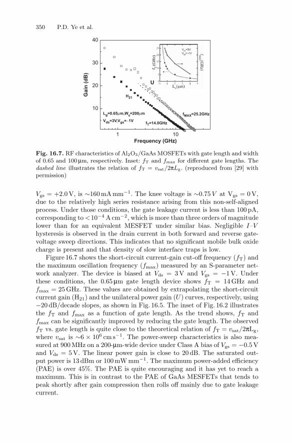
350 P.D. Ye et al.
1 10
10
20
30
40
Lg=0.65µm,Wg=200µm
Vds=3V,Vgs=−1V
U
H21
fT=14.0GHz
fMAX=25.2GHz
Gai
n (d
B)
Frequency (GHz)
Fig. 16.7. RF characteristics of Al2O3/GaAs MOSFETs with gate length and widthof 0.65 and 100 µm, respectively. Inset: fT and fmax for different gate lengths. Thedashed line illustrates the relation of fT = vsat/2πLg. (reproduced from [29] withpermission)
Vgs = +2.0V, is ∼160mA mm−1. The knee voltage is ∼0.75V at Vgs = 0V,due to the relatively high series resistance arising from this non-self-alignedprocess. Under those conditions, the gate leakage current is less than 100 pA,corresponding to <10−4 Acm−2, which is more than three orders of magnitudelower than for an equivalent MESFET under similar bias. Negligible I–Vhysteresis is observed in the drain current in both forward and reverse gate-voltage sweep directions. This indicates that no significant mobile bulk oxidecharge is present and that density of slow interface traps is low.
Figure 16.7 shows the short-circuit current-gain cut-off frequency (fT) andthe maximum oscillation frequency (fmax) measured by an S-parameter net-work analyzer. The device is biased at Vds = 3 V and Vgs = −1 V. Underthese conditions, the 0.65 µm gate length device shows fT = 14GHz andfmax = 25GHz. These values are obtained by extrapolating the short-circuitcurrent gain (H21) and the unilateral power gain (U) curves, respectively, using−20 dB/decade slopes, as shown in Fig. 16.5. The inset of Fig. 16.2 illustratesthe fT and fmax as a function of gate length. As the trend shows, fT andfmax can be significantly improved by reducing the gate length. The observedfT vs. gate length is quite close to the theoretical relation of fT = vsat/2πLg,where vsat is ∼6 × 106 cm s−1. The power-sweep characteristics is also mea-sured at 900 MHz on a 200-µm-wide device under Class A bias of Vgs = −0.5Vand Vds = 5V. The linear power gain is close to 20 dB. The saturated out-put power is 13 dBm or 100mW mm−1. The maximum power-added efficiency(PAE) is over 45%. The PAE is quite encouraging and it has yet to reach amaximum. This is in contrast to the PAE of GaAs MESFETs that tends topeak shortly after gain compression then rolls off mainly due to gate leakagecurrent.

16 Characterization of III–V Compound Semiconductor MOSFETs 351
−2.0 −1.5 −1.0 −0.5 0.0 0.5 1.0 1.5 2.00
20
40
60
80
100
120
140
160
180
200
0
10
20
30
40
50
60
70
80
90
100
g m(m
S/m
m)
I ds(
mA
/mm
)
Vgs(V)
Lg=1µm
Wg=100µm
Vds=3V
Fig. 16.8. Drain current vs. gate bias in both forward (empty squares) and reverse(filled squares) sweep directions. Circles are transconductances vs. gate bias at Vds =3V. (reproduced from [30] with permission)
Figure 16.8 illustrates the drain current as a function of gate bias in thesaturation region. The slope of the drain current shows that the peak ex-trinsic transconductance (gm) of the 1 µm gate length device is typically∼100mS mm−1. It can be improved to ∼130mS mm−1 by reducing the gatelength to 0.65 µm. The theoretical intrinsic gm in saturation regime can be es-timated to be ∼280mS mm−1 by gm = υsat ·Cox, where υsat is ∼6×106 cm s−1.Considering the series resistance of the device Rs ∼ 2.5Ωmm, the theoreticalextrinsic gm is ∼165mS mm−1 which is ∼20% off from the measured peakgm value. We ascribe this reduction of gm to the existing interface traps andthe reduction of mobility and saturation velocity at the interface. It is alsopossible to give a rough estimation of Dit using the hysteresis from Ids vs.Vgs traces [30]. For ∆Vgs of 30 mV shown in Fig. 16.8, the estimated Dit is6× 1010/cm2-eV, which is at the lower side of the Dit evaluation. We ascribethe smaller hysteresis observed at the device level here, compared to C–Vmeasurements described above, to the very small gate area and more leakagecurrent in oxide after full device process.
Figure 16.9a shows the peak gm as a function of frequency, measured fromDC to several GHz, under typical operating conditions (Vds = 3 V, Vgs =−1V). The measurements are performed by three different experimental set-ups. The DC and RF (MHz–GHz) measurements are performed by a standardparameter analyzer and a microwave network analyzer, respectively. Data inthe kHz range is obtained by a signal generator and a lock-in amplifier. It canbe seen that the gm remains essentially constant for frequencies above 20 Hz,indicating that efficient charge modulation in the channel can be achieved overthe entire useful frequency range of the device. Furthermore, note that thereis about a 20% decrease in gm from 20 Hz down to DC. Figure 16.9b shows themodel calculation based on all available device parameters. The y-axis is themaximum change of gm(gm min/gm max) between DC and GHz frequencies.

352 P.D. Ye et al.
(a) (b)
100
101
102
103
104
105
106
107
108
109
0
25
50
75
100
125
150
175
200
dc gm(0)
dropfrom f
T
Data measuredfrom microwave network analyzer
data measuredfrom signalgenerator
g m(m
S/m
m)
f (Hz)
Lg=0.65µm
Wg=100µm
Vds=3V
−4 −3 −2 −1 00.0
0.2
0.4
0.6
0.8
1.0
g m m
in/g
m m
ax
Vgs(V)
N=4E17/cm3 Tox=160Å
Dit=1E10/cm2eV
Dit=1E11/cm2eV
Dit=2E11/cm2eV
Dit=5E11/cm2eV
Dit=1E12/cm2eV
Dit=2E12/cm2eV
Dit=5E12/cm2eV
Dit=1E13/cm2eV
Fig. 16.9. (a) Peak transconductance gm vs. frequency from DC to several GHz.The gm is essentially constant for frequencies above 20Hz. Vgs is biased at thepeak gm. (b) Model calculations of gm due to the effects of Dit. Eighty percent ofgm min g−1
m max at −2 V < Vgs < 0V, as shown in (a), corresponds to Dit between5 × 1011 to 1012 cm−2 eV−1. gm min is gm at DC and gm max is the maximum gm ata few GHz before fT in real devices. (reproduced from [30] with permission)
If the device has very low Dit, e.g., 1 × 1010 cm−2 eV−1 as the solid line inFig. 16.9(b), then gm is almost constant. The maximum change of gm is nearzero and gm min/gm max is 1. The model calculation of our devices in gm givesan upper limit for Dit of 5 × 1011 cm−2 eV−1.
16.5 InGaAs MOSFET Fabrication and Characterization
InAs has a room temperature electron mobility as high as 20,000 cm2 Vs−1.Although InAs layers can be formed on GaP or InP substrates, the tech-nology is not mature for commercialization. InGaAs has a mobility betweenInAs and GaAs. InGaAs is widely used in compound semiconductors to im-prove the channel mobility, and thereby improve the device performance.In0.53Ga0.47As layers, which are lattice-matched to InP, are used as electronchannels for InP HEMTs. The strained thin layer of In0.2Ga0.8As is widelyused for pseudomorphic HEMTs (p-HEMTs). A depletion-mode n-channelAl2O3/In0.2Ga0.8As/GaAs MOSFET was fabricated using a process similarto that described earlier in this chapter, on GaAs MOSFETs. A 1,500 A un-doped GaAs buffer layer, a 140 A Si-doped GaAs layer (2× 1018 cm−3), and a135 A Si-doped In0.2Ga0.8As layer (1×1018 cm−3) were subsequently grown byMBE on a (100)-oriented semi-insulating 2-in. GaAs substrate. Figure 16.10shows the DC I–V curve of an InGaAs MOSFET with a gate length Lg of1 µm and a gate width Wg of 100 µm. The gate voltage was varied from -4.0 to+3.0V with 1.0 V steps. Figure 16.10 has 1.0V steps for the gate voltage. Thefabricated device has a pinch-off voltage of −4.0 V. The maximum drain cur-rent density Idss, measured at positive bias Vgs = +3.0V, is ∼330mA mm−1.

16 Characterization of III–V Compound Semiconductor MOSFETs 353
0.0 0.5 1.0 1.5 2.0 2.5 3.00
5
10
15
20
25
30
35Lg=1µm
Wg=100µm
−4V
Vg=+3V
−3V
−2V
−1V
0V
+1V
+2V
I ds(
mA
)
Vds(V)
Fig. 16.10. Drain current vs. drain bias as a function of gate bias (reproducedfrom [33] with permission)
The knee voltage is ∼1.0V at Vgs = 0V, due to the relatively high seriesresistance arising from this non-self-aligned process. Under those conditions,the gate leakage current is less than 100 pA, corresponding to <10−4 Acm−2.Much more accumulation current (∼200mA mm−1) is observed in InGaAsMOSFET at positive gate bias, compared to GaAs MOSFET. It might in-dicate a better interface on InGaAs or the Dit at conduction band edge ofAl2O3/In0.2Ga0.8As is better than that at Al2O3/GaAs. Since there is noSchottky barrier between metal-InGaAs or metal-InAs, the MOS structurediscussed here could be the only way to realize InGaAs or InAs MOSFETs.
16.6 GaN MOS-HEMT Fabrication and Characterization
One of the major factors that limit the performance and reliability of GaNHEMTs for high-power radio-frequency (RF) applications is their relativelyhigh gate leakage. The gate leakage reduces the breakdown voltage and thepower-added efficiency while increasing the noise figure. To help solve theproblem, significant progress has been made on MIS-HEMTs and MOS-HEMTs using SiO2 [53–57], Si3N4 [58, 59], Al2O3 [60, 61] (formed by elec-tron cyclotron resonance plasma oxidation of Al), and other oxides [62].However these gate dielectrics and their associated processes may not be read-ily scalable for low-cost and high-yield manufacture. The thickness control ofthe ALD films, and thus scalability, is much superior than those of the plasma-enhanced-chemical-vapor-deposition (PECVD) grown SiO2 and Si3N4. Thequality of the ALD Al2O3 is also much higher than those deposited by othermethods, i.e., sputtering and electron-beam deposition, in terms of uniformity,defect density and stoichiometric ratio of the films.
ALD Al2O3/AlGaN/GaN MOS-HEMT process is similar with the de-vice process we discussed above. A 40 nm undoped AlN buffer layer, a 3 µm

354 P.D. Ye et al.
0 20 40 60 80 1000
50
100
150
200
250
300
350
400
5V
−4V−3V−2V
−1V0
1V
2V
3V4V
Vgs=6V GaN MOS-HEMT
Al2O3 16nm
Lg=5µm
I ds(
mA
/mm
)
Vds(V)
Fig. 16.11. Measured I–V characteristics of a GaN MOS-HEMT using ALD Al2O3.The negative output conductance under high gate biases (Vgs ≥ 0) is due to selfheating. (reproduced from [34] with permission)
undoped GaN layer, and a 30 nm undoped Al0.2Ga0.8N layer were sequentiallygrown by metal-organic chemical vapor deposition on a 2-in. sapphire sub-strate. A 16 nm thick Al2O3 layer was deposited at 300C then followed by an-nealing at 600C for 60 s in oxygen ambient. Device isolation was achieved bynitrogen implantation. Using a wet etch in diluted HF, the oxide on the sourceand drain regions was removed while the gate region was protected by photore-sist. Ohmic contacts were formed by electron-beam deposition of Ti/Al/Ni/Auand a lift-off process, followed by an 850C anneal in a nitrogen ambient, whichalso activated the previously implanted nitrogen. Finally, Ni/Au metals weree-beam evaporated and lifted off to form the gate electrodes.
Figure 16.11 shows that the I–V characteristics of the MOS-HEMT arewell behaved over a drain bias Vds of 0–100 V and a gate bias Vgs of −4 to6 V. The pinch-off voltage is consistently −4V. The maximum drain currentdensity Ids/Wg at Vgs = 6V is approximately 375 mA mm−1. The off-statethree-terminal breakdown voltage is approximately 145 V. The results indicatethat ALD Al2O3 is an effective gate dielectric for AlGaN/GaN devices. Ourdevices have no widely observed abnormal I–V characteristics at positive gatebiases, i.e., PECVD grown SiO2 GaN MOS-HEMTs [48], which are mostlyrelated with the bulk traps in PECVD grown dielectrics or interface traps atinsulating films on GaN.
Figures 16.12a,b illustrate the saturated (Vds = 10 V) drain current den-sity and intrinsic transconductance gm as a function of gate bias for both theMOS-HEMT and the HEMT. The drain current density of the HEMT is lim-ited to 190 mA mm−1 at Vgs = 2 V. By contrast, the drain current density ofthe MOS-HEMT is 450 mA mm−1 at Vgs = 8V and can be further increasedunder higher Vgs. The combination of higher breakdown voltage and higherdrain current imply that the output power of the MOS-HEMT can be muchhigher than that of the HEMT. Using Ids/Wg = e ns υsat = 450mA mm−1
and a saturated velocity υsat = 5 × 106 cm s−1, the sheet carrier density

16 Characterization of III–V Compound Semiconductor MOSFETs 355
(a) (b)
400
300
200
100
0
I ds(
mA
/mm
)
86420−2−4
Vgs(V)
MOS-HEMT
HEMT
120
100
80
60
40
20
0
g m (
mS/
mm
)
86420−2−4Vgs(V)
HEMTMOSHEMT
Fig. 16.12. Measured (a) transfer and (b) transconductance characteristics mea-sured with the MOS-HEMT (solid line) and HEMT (dashed line) in saturation(Vds = 10V). (reproduced from [34] with permission)
ns is estimated to be 6 × 1012 cm−2, which is within the range of valuescommonly observed for the heterojunction between undoped Al0.2Ga0.8Nand GaN. Figure 16.12b shows that the peak gm is 100 and 120 mS mm−1
for the MOS-HEMT and the HEMT, respectively. The gm was calculatedfrom the measured extrinsic transconductance by accounting for the para-sitic source resistance Rs of 5.4 and 5.9 Ω mm for the MOS-HEMT and theHEMT, respectively. The Rs values were measured on test structures fabri-cated alongside the MOS-HEMT and the HEMT according to the transmis-sion line method (TLM). These gm values are in agreement with theoreticalestimates according to gm = υsat · CMOS−HEMT or gm = υsat · CHEMT. Usingυsat = 5 × 106 cm s−1, CMOS−HEMT = 16pF, and CHEMT = 21pF, gm wasestimated to be 102 and 133 mS mm−1 for the MOS-HEMT and the HEMT,respectively. The sheet resistances measured on TLM test structures are 700and 950Ω sq.−1 for the MOS-HEMT and the HEMT, respectively.
The present Al2O3/AlGaN/GaN heterojunction enables us to measure theeffective 2D electron mobility µeff at the AlGaN/GaN heterojunction underhigh electron density and high transverse field as shown in Fig. 16.13. The 2Delectron mobility is governed by Coulomb scattering and phonon scatteringunder low transverse field. It is dominated by interface roughness scatteringand phonon scattering under strong accumulation. The resulting mobility of1,200 cm2 Vs−1 under low transverse fields is consistent with the value ob-tained from the Hall measurement. The mobility of 640 cm2 V s−1 under ahigh transverse field of 0.6 MVcm−1 is much higher than 400 cm2 V s−1, theuniversal mobility of Si MOSFETs under the same field. It is also higher thanthe surface mobility of GaAs or InGaAs MOSFETs we observed earlier. Suchan improvement can be attributed to the higher quality of the AlGaN/GaNsemiconductor–semiconductor interface than that of the oxide–semiconductorinterfaces. The details how to obtain the µeff vs. Eeff are described in [33]and [34].
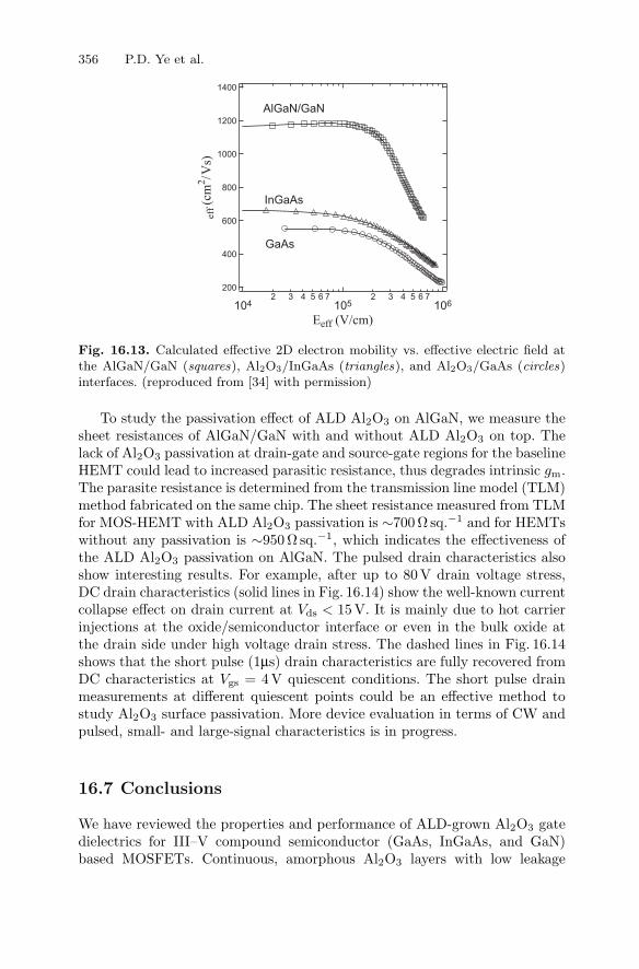
356 P.D. Ye et al.
1400
1200
1000
800
600
400
200
eff
(cm
2/V
s)
1042 3 4 5 6 7
1052 3 4 5 6 7
106
Eeff (V/cm)
AlGaN/GaN
InGaAs
GaAs
Fig. 16.13. Calculated effective 2D electron mobility vs. effective electric field atthe AlGaN/GaN (squares), Al2O3/InGaAs (triangles), and Al2O3/GaAs (circles)interfaces. (reproduced from [34] with permission)
To study the passivation effect of ALD Al2O3 on AlGaN, we measure thesheet resistances of AlGaN/GaN with and without ALD Al2O3 on top. Thelack of Al2O3 passivation at drain-gate and source-gate regions for the baselineHEMT could lead to increased parasitic resistance, thus degrades intrinsic gm.The parasite resistance is determined from the transmission line model (TLM)method fabricated on the same chip. The sheet resistance measured from TLMfor MOS-HEMT with ALD Al2O3 passivation is ∼700Ω sq.−1 and for HEMTswithout any passivation is ∼950Ω sq.−1, which indicates the effectiveness ofthe ALD Al2O3 passivation on AlGaN. The pulsed drain characteristics alsoshow interesting results. For example, after up to 80 V drain voltage stress,DC drain characteristics (solid lines in Fig. 16.14) show the well-known currentcollapse effect on drain current at Vds < 15V. It is mainly due to hot carrierinjections at the oxide/semiconductor interface or even in the bulk oxide atthe drain side under high voltage drain stress. The dashed lines in Fig. 16.14shows that the short pulse (1µs) drain characteristics are fully recovered fromDC characteristics at Vgs = 4V quiescent conditions. The short pulse drainmeasurements at different quiescent points could be an effective method tostudy Al2O3 surface passivation. More device evaluation in terms of CW andpulsed, small- and large-signal characteristics is in progress.
16.7 Conclusions
We have reviewed the properties and performance of ALD-grown Al2O3 gatedielectrics for III–V compound semiconductor (GaAs, InGaAs, and GaN)based MOSFETs. Continuous, amorphous Al2O3 layers with low leakage

16 Characterization of III–V Compound Semiconductor MOSFETs 357
0 2 4 6 8 10 12 140
50
100
150
200
250
300 MOS-HEMT Vg=4V step - 1VLg=0.65µm
DC 1µs
I ds(
mA
/mm
)
Vds(V)
Fig. 16.14. Output I–V characteristics of MOS-HEMT under DC (solid line) and1 µs pulsed-gate bias (dashed line). The pulse width is 1 µs with 10% duty cycle
current and high breakdown strength may be grown by ALD. Through a com-bination of surface preparation (e.g., HF etching), choice of a reactive ALDprecursor, and thermal processing at ∼600C, Al2O3/GaAs stacks with lowinterfacial layer thickness can be fabricated. For GaAs MOSFET, submicrongate-length devices exhibit an extrinsic transconductance up to 130 mS mm−1,with negligible I–V hysteresis and a gate leakage current density less than10−4 Acm−2. The RF characteristics of an 0.65 µm gate-length device showsan fT of 14 GHz and an fmax of 25 GHz. Through the drain current hys-teresis, we obtain 6 × 1010 cm−2 eV−1 as the lower limit of the interface trapdensity (Dit) of Al2O3/GaAs. The upper limit of Dit of 5 × 10¹¹/cm2 eVis obtained by transconductance vs. frequency measurements and modeling.InGaAs MOSFET shows a stronger accumulation current, indicating a bet-ter interface between Al2O3 and InGaAs. ALD Al2O3 process also provideshigh-quality gate dielectric and surface passivation for AlGaN/GaN HEMTs.The resulted MOS-HEMT shows favorable characteristics when compared toMOS-HEMTs with other gate insulators. These results suggest new opportu-nities for providing processing alternatives, including high-κ gate dielectricsand passivation layers, by ALD for III–V semiconductor devices.
Acknowledgments
The authors would like to thank B. Yang, K.K. Ng, J.D. Bude, M. Hong, H.-J.L. Gossmann, M. Frei, J. Kwo, J.P. Mannaerts, J.C.M. Hwang, S. Halder,D.A. Muller, D. Starodub, T. Gustafsson, E. Garfunkel, Y.J. Chabal, H.C.Lin, and Y. Tokuda for their contributions.
358 P.D. Ye et al.
References
1. T. Mimura and M. Fukuta, “Status of the GaAs Metal-Oxide-SemiconductorTechnology”, IEEE Trans. Electron Devices, vol. ED-27, pp. 1147–1155, 1980,and references therein
2. “Physics and Chemistry of III–V Compound Semiconductor Interfaces”, Ed.C.W. Wilmsen, Plenum, New York, 1985, and references therein
3. “Semiconductor-insulator interfaces”, M. Hong, C.T. Liu, H. Reese, and J. Kwoin “Encyclopedia of Electrical and Electronics Engineering”, volume 19, pp.87–100, Ed. J.G. Webster, Published by John Wiley & Sons, New York, 1999,and references therein
4. S. Tiwari, S.L. Wright, and J. Batey, “Unpinned GaAs MOS capacitors andtransistors”, IEEE Electron Devices Lett., 9, pp. 488–490, 1988
5. C.L. Chen, F.W. Smith, B.J. Clifton, L.J. Mahoney, M.J. Manfra, and A.R.Calawa, “High-Power-Density GaAs MISFET’s with a low-temperature-grownepitaxial layer as the insulator”, IEEE Electron Devices Lett., 12, pp. 306–308,1991
6. Y.H. Jeong, K.H. Choi, and S.K. Jo, “Sulfide treated GaAs MISFET’s withgate insulator of photo-CVD grown P3N5 film”, IEEE Electron Devices Lett.,15, pp. 251–253, 1994
7. E.I. Chen, N. Holonyak, and S.A. Maranowski, “AlxGa1-xAs-GaAs metal-oxidesemiconductor field effect transistors formed by lateral water vapor oxidation ofAlAs”, Appl. Phys. Lett., 66, pp. 2688–2690, 1995
8. J.Y. Wu, H.H. Wang, Y.H. Wang, and M.P. Houng, “A GaAs MOSFET with aliquid phase oxidized gate”, IEEE Electron Devices Lett., 20, pp. 18–20, 1999
9. T. Waho and F. Yanagawa, “A GaAs MISFET using an MBE-grown CaF2 gateinsulator layer”, IEEE Electron Devices Lett., 9, pp. 548–549, 1988
10. G.W. Pickrell, J.H. Epple, K.L. Chang, K.C. Hsieh, and K.Y. Cheng, “Improve-ment of wet-oxidized AlxGa1−xAs(x∼1) through the use of AlAs/GaAs digitalalloys”, Appl. Phys. Lett., 76, pp. 2544–2546, 2000
11. J.C. Ferrer, Z. Liliental-Weber, H. Reese, Y.J. Chiu, and E. Hu, “Improvementof the interface quality during thermal oxidation of Al0.98Ga0.02As layers dueto the presence of low-temperature-grown GaAs”, Appl. Phys. Lett., 77, pp.205–207, 2000
12. S. Yokoyama, K. Yukitomo, M. Hirose, Y. Osaka, A. Fischer, and K. Ploog,“GaAs MOS structures with Al2O3 grown by molecular beam reaction”, Surf.Sci., 86, pp. 835–840, 1979
13. J. Reed, G.B. Gao, A. Bochkarev, and H. Morkoc, “Si3N4/Si/Ge/GaAs metal-insulator-semiconductor structures grown by in situ chemical vapor deposition”,J. Appl. Phys., 75, pp.1826–1828, 1994
14. B.J. Skromme, C.J. Sandroff, E. Yablonovitch, and T. Gmitter, Appl. Phys.Lett. 51, 2022 (1987)
15. G.G. Fountain, R.A. Rudder, S.V. Hattangady, R.J. Markunas, and J.A.Hutchby, IEDM Tech, Dig. 887 (1989)
16. M. Akazawa, H. Ishii, and H.Hasegawa, Jpn. J. Appl. Phys., Part 1 30, 3744(1991)
17. A. Callegari, P.D. Hoh, D.A. Buchanan, and D. Lacey, Appl. Phys. Lett. 54,332 (1989)
18. S.D. Offsey, J.M. Woodall, A.C. Warren, P.D. Kirchner, T.I. Chappell, and G.D.Pettit, Appl. Phys. Lett. 48, 475 (1986)

16 Characterization of III–V Compound Semiconductor MOSFETs 359
19. M.J. Hale, S.I. Yi, J.Z. Sexton, A.C. Kummel, and M. Passlack, J. Chem. Phys.119, 6719 (2003)
20. W.E. Spicer, Z. Liliental-Weber, E. Weber, N. Newman, T. Kendelewicz, R. Cao,C. McCants, P. Mahowald, K. Miyano, and I. Lindau, J. Vac. Sci. Technol. B6, 1245 (1988)
21. K. Eguchi and T. Katoda, Jpn. J. Appl. Phys. 24, 1043 (1985)22. M. Hong, M. Passlack, J.P. Mannaerts, J. Kwo, S.N.G. Chu, N. Moriya, S.Y.
Hou, and V.J. Fratello, “Low interface state density oxide-GaAs structures fab-ricated by in situ molecular beam epitaxy”, J. Vac. Sci. Technol. B, 14, pp.2297–2300, 1996
23. M. Passlack, M. Hong, J.P. Mannaerts, R.L. Opila, S.N.G. Chu, N. Moriya, F.Ren, J.R. Kwo, “ Low Dit, thermodynamically stable Ga2O3-GaAs interfaces:Fabrication, characterization, and modeling”, IEEE Trans. Electron Devices,44, pp. 214–225, 1997
24. M. Hong, J. Kwo, A.R. Kortan, J.P. Mannaerts, and A.M. Sergent, “Epitax-ial cubic Gadolinium oxide as a dielectric for Gallium Arsenide passivation”,Science, 283, pp. 1897–1900, 1999
25. J. Kwo, D.W. Murphy, M. Hong, R.L. Opila, J.P. Mannaerts, A.M. Sergent, andR.L. Masaitis, “Passivation of GaAs using (Ga2O3)1−x(Gd2O3)x, 0 < x < 1.0films”, Appl. Phys. Lett., 75, pp. 1116–1118, 1999
26. F. Ren, M. Hong, W.S. Hobson, J.M. Kuo, J.R. Lothian, J.P. Mannaerts, J.Kwo, S.N.G. Chu, Y.K. Chen, and A.Y. Cho, “Demonstration of enhancement-mode p- and n-channel GaAs MOSFETs with Ga2O3(Gd2O3) as gate oxide”,Solid-State Electron., 41, pp. 1751–1753, 1997
27. Y.C. Wang, M. Hong, J.M. Kuo, J.P. Mannaerts, J. Kwo, H.S. Tsai, J.J. Kra-jewski, Y.K. Chen, and A.Y. Cho, “Demonstration of submicron depletion-modeGaAs MOSFET’s with negligible drain current drift and hysteresis”, IEEE Elec-tron Devices Lett., 20, pp. 457–459, 1999
28. M. Passlack, J.K. Abrokwah, R. Droopad, Z. Yu, C. Overgaard, S. I. Yi, M.Hale, J. Sexton, and A.C. Kummel, “Self-aligned GaAs p-channel enhancementmode MOS heterostructure field-effect transistor”, IEEE Electron Devices Lett.,23, pp. 508–510, 2002
29. P.D. Ye, G.D. Wilk, J. Kwo, B. Yang, H.-J.L. Gossmann, M. Frei, S.N.G. Chu,J.P. Mannaerts, M. Sergent, M. Hong, K. Ng, J. Bude, “GaAs MOSFET withoxide gate dielectric grown by atomic layer deposition”, IEEE Electron DeviceLett., 24, No.4, 209 (April 2003)
30. P.D. Ye, G.D. Wilk, J. Kwo, B. Yang, H.-J.L. Gossmann, M.R. Frei, S.N.G. Chu,S. Nakahara, J.P. Mannaerts, M. Sergent, M. Hong, K. Ng, J. Bude, “GaAs-based MOSFETs with Al2O3 gate dielectrics grown by atomic layer deposition”,J. Electronic Mater., 33, No.8, 912–915 (Aug 2004)
31. P.D. Ye, G.D. Wilk, B. Yang, J. Kwo, S.N.G. Chu, S. Nakahara, H.-J.L. Goss-mann, J.P. Mannaerts, M. Hong, K. Ng, J. Bude, “GaAs MOSFET with nm-thindielectric grown by atomic layer deposition”, Appl. Phys. Lett. 83, 180 (2003)
32. P.D. Ye, G.D. Wilk, B. Yang, S.N.G. Chu, H.-J.L. Gossmann, K. Ng, J. Bude,“Improvement of GaAs MESFET drain breakdown voltage by oxide surfacepassivation grown by atomic layer deposition”, Solid State Electron., 49, Issue5, 790–794 (May 2005)
33. P.D. Ye, G.D. Wilk, B. Yang, J. Kwo, H.-J.L. Gossmann, M. Hong, K. Ng, J.Bude, “Depletion-mode InGaAs MOSFET with oxide gate dielectric grown byatomic layer deposition”, Appl. Phys. Lett. 84, January 17 (2004)

360 P.D. Ye et al.
34. P.D. Ye, B. Yang, K.K. Ng, J. Bude, G.D. Wilk, S. Halder and J.C.M. Hwang“GaN MOS-HEMT with atomic layer deposition Al2O3 as gate dielectric”, Appl.Phys. Lett. 86, 063501 (2005).
35. P.D. Ye, G.D. Wilk, E. Tois, and J.J. Wang, “Formation and characterizationof nanometer scale metal-oxide-semiconductor structures on GaAs using low-temperature atomic layer deposition”, Appl. Phys. Lett. 87, (July 4, 2005).
36. G.D. Wilk, R.M. Wallace, and J.M. Anthony, “High-k gate dielectrics: Currentstatus and materials properties considerations”, J. Appl. Phys., 89, pp. 5243–5275, 2001.
37. Martin M. Frank, Glen D. Wilk, Dmitri Starodub, Torgny Gustafsson, EricGarfunkel, Yves J. Chabal, John Grazul, and David A. Muller, “HfO2 and Al2O3
gate dielectrics on GaAs grown by atomic layer deposition”, Appl. Phys. Lett.86, 152904 (2005)
38. K. Tone, M. Yamada, Y. Ide, and Y. Katayama, Jpn. J. Appl. Phys., Part 231, L721 (1992)
39. F. Schroder, W. Storm, M. Altebockwinkel, L. Wiedmann, and A. Bennighoven,J. Vac. Sci. Technol. B 10, 1291 (1992)
40. S. Adachi and D. Kikuchi, J. Electrochem. Soc. 147, 4618 (2000)41. A. Delabie, R.L. Puurunen, B. Brijs, M. Caymax, T. Conard, B. Onsia, O.
Richard, W. Vandervorst, C. Zhao, M.M. Viitanen, H.H. Brongersma, M. deRidder, L.V. Goncharova, E. Garfunkel, T. Gustafsson, W. Tsai, M.M. Heyns,and M. Meuris, J. Appl. Phys., submitted
42. D.R. Lide, CRC Handbook of Chemistry and Physics, 85 ed. (CRC Press, BocaRaton, 2004)
43. I. Barin and O. Knacke, Thermochemical Properties of Inorganic Substances.(Springer-Verlag, Berlin, 1973)
44. M.D. Groner, J.W. Elam, F.H. Fabreguette, and S.M. George, Thin Solid Films413, 186 (2002)
45. W.S. Yang, Y.K. Kim, S.Y. Yang, J.H. Choi, H.S. Park, S.I. Lee, J.B. Yoo, Surf.Coat. Tech. 131, 79 (2000)
46. G.S. Higashi and C.G. Fleming, Appl. Phys. Lett. 55, 1963 (1989)47. J. Fan, K. Sugioka, K. Toyoda, Jpn. J. Appl. Phys. 30, L1139 (1991)48. H. Kattelus, M. Ylilammi, J. Saarilahti, J. Antson, S. Lindfors, Thin Solid Films
225, 296 (1993)49. K. Kukli, M. Ritala, M. Leskela and J. Jokinene, J. Vac. Sci. Technol. A 15,
2214 (1997)50. P. Ericsson, S. Bengtsson, and J. Skarp, Microelectron. Eng. 36, 91 (1997)51. V.E. Drozd, A.P. Baraban and I.O. Nikiforova, Appl. Surf. Sci. 82/83, 583
(1994)52. Zhijiong Luo and T.P. Ma, “A New Method to Extract EOT of Ultrathin Gate
Dielectric With High Leakage Current”, IEEE Electron Device Lett., 25, No.9,655 (2004)
53. M. Asif Khan, X. Hu, G. Sumin, A. Lunev, J. Yang, R. Gaska, and M.S. Shur,IEEE Electron Devices Lett. 21, 63 (2000)
54. M. Asif Khan, X. Hu, A. Tarakji, G. Simin, J. Yang, R. Gaska, and M.S. Shur,Appl. Phys. Lett, 77, 1339 (2000)
55. G. Simon, X. Hu, N. Ilinskaya, A. Kumar, A. Koudymov, J. Zhang, M.A. Khan,R. Gaska, and M.S. Shur, Electronics Lett. 36, 2043 (2000)
56. A. Koudymov, X. Hu, K. Simin, G. Simin, M. Ali, J. Yang, and M. Asif Khan,IEEE Electron Devices Lett., 23, 449 (2002)

16 Characterization of III–V Compound Semiconductor MOSFETs 361
57. G. Simin, A. Koudymov, H. Fatima, J. Zhang, J. Yang, and M. Asif Khan, X.Hu, A. Tarakji, R. Gaska, and M.S. Shur, IEEE Electron Devices Lett. 23, 458(2002)
58. G. Simon, X. Hu, N. Ilinskaya, J. Zhang, A. Tarakji, A. Kumar, J. Yang, M.Asif Khan, R. Gaska, and M.S. Shur, IEEE Electron Devices Lett. 22, 53 (2001)
59. X. Hu, A. Koudymov, G. Simon, J. Yang, M. Asif Khan, A. Tarakji, M.S. Shur,and R. Gaska, Appl. Phys. Lett, 79, 2832 (2000)
60. S. Ootomo, T. Hashizume, and H. Hasegawa, phys. stat. sol. (c) 1, 90 (2002).61. T. Hashizume, S. Ootomo, and H. Hasegawa, Appl. Phys. Lett. 83, 2952 (2003)62. R. Mehandru, B. Luo, J. Kim, F. Ren, B.P. Gila, A.H. Onstine, C.R. Abernathy,
S.J. Pearton, D. Gotthold, R. Birkhahn, B. Peres, R. Fitch, J. Gillespie, T.Jenkins, J. Sewell, D. Via and A. Crespo, Appl. Phys. Lett. 82, 2530 (2003)

17
Fabrication of MBE High-κ MOSFETsin a Standard CMOS Flow
L. Pantisano, T. Conard, T. Scram, W. Deweerd, S. De Gendt, M. Heyns,Z.M. Rittersma, C. Marchiori, M. Sousa, J. Fompeyrine, and J.-P. Locquet
Summary. For the first time MOSFET transistor performance featuring dielectricLanthanum Hafnium Oxide (LHO) deposited by molecular beam epitaxy are pre-sented. These dielectrics were deposited on a SiO2-like surface and integrated into aconventional etched-gate flow featuring TaN as gate electrode. The results for refer-ence HfO2 deposited in the same MBE tool are comparable to standard (atomic layerdeposited) HfO2 in the same process flow. Long-channel LHO devices exhibit rea-sonably good performance, while short-channel devices are sensitive to some processissues. LHO devices exhibit excellent leakage and minimal Vt-instability comparedto HfO2.
17.1 Introduction
In the recent years tremendous research efforts have been focused on the in-vestigation of so-called high-κ gate dielectrics for the potential replacement ofSiO2 in advanced CMOS technologies [1–3]. The high-κ oxides allow the fur-ther increase of the gate capacitance without paying the price of an increasedleakage current (and thus dissipated power). Several materials have been suc-cessfully used as high-κ dielectrics [1] using deposition techniques such asPVD (physical vapor deposition)-based or CVD (chemical vapor deposition)-based [2]. These materials were integrated in conventional MOSFET usingeither conventional etched gate or replacement-gate with either poly-Si [3] ormetal as gate dielectrics.
For the first time in this paper we report results on n-channel MOS-FET with LHO integrated in a conventional etched-gate flow. This paperis organized as following. After the section on the device fabrication is-sues, the electrical results in these devices are discussed. Due to nonideali-ties during the fabrication process, there is a significant difference betweenthe long- and short-channel devices. These devices further exhibit negligiblehysteresis.

364 L. Pantisano et al.
SHORT TITLE
TiSi2
8” p-(n-) SiSTI isolation
PVD TaN / TiN
LDD/ Spacer Dep /HDD ImplantActivation @ 900 ºC (LHO) or 1000 ºC spike (HfO2)
Surface preparationSiON
High-k deposition LHO
HfO2No PDA
Gate Patterning EtchPolymerremoval
standardNo chemistry found
HF-last + Flash O2
Fig. 17.1. Processing steps for gate stack integration
17.2 Device Fabrication
La2Hf2O7 (LHO in the following) devices were fabricated using a conventionaletched-gate scheme (see Fig. 17.1). Bare Si(001) wafer with an “HF-last” or“SiON” surface treatment were used as starting surface. Before deposition, thesurface of the wafers was cleaned in situ, either using a moderate or a hightemperature-degassing step. The 8 in. molecular beam epitaxy (MBE) toolfrom RIBER (France) is equipped with an atomic oxygen source from OxfordApplied Research (UK). Either LHO or HfO2 were deposited in this experi-ment as described in earlier publications [4]. The oxide target thickness was inthe 3–6 nm range in both cases. No postdeposition anneal was performed. The10 nm TaN were deposited after 2 weeks from the deposition. Figure 17.1 sum-marizes the process flow. 70 nm TiN was used as a contact metal. After resistdeposition for patterning a standard etching was done. Since LHO dissolvesin water, no resist cleaning was done. Note that an encapsulating spacer wasused [5] to protect the metal gate during subsequent processing. The processwas completed by junction implant (LDD, HDD, and spacer). TiSi junctionswere used in this work. A “conservative” junction activation annealing stepwas done at 900 C for 10 s. As final fabrication step these devices have seena forming gas annealing at 520C for 30 min.
17.2.1 TEM Pictures and Salient Features
The fabrication of these devices was problematic, as shown in Fig. 17.2 forHfO2 and Fig. 17.3 for LHO. For HfO2 (see Fig. 17.2) the interfacial layerthickness varies between 11 and 14 A, being thicker close to edge of the gate

17 Fabrication of MBE High-κ Mosfets 365
Fig. 17.2. TEM picture of an HfO2 device. The inset shows a magnification of thechannel region
(i.e., bird’s beaks). Despite the poor contrast the HfO2 thickness is of theorder of 3 nm (as expected). Due to an unoptimized silicidation, a large recessis observable. This effect has a severe impact on the series resistance of theMOSFET considered, as will be discussed in the following sections.
Similar observation can be made for the LHO sample (see Fig. 17.3). Theinterfacial oxide thickness is in the order of 7 A. Note that the LHO is 4 nmunder the spacers. The drain and source junctions further show a quite steepetching, with further recess and bad uniformity.
17.3 Device Characterization
Most of the devices tested were yielding and operational. However in mostcases it was found that long-channel devices did not have ideal MOSFET char-acteristics, conversely to many similar lots processed the same way. It is likelythat some of the differences observed are linked to the process flow and/orpossible interfacial oxide regrowth during processing. Some of the electrical
Fig. 17.3. TEM picture of an LHO device. The inset shows a magnification of thechannel

366 L. Pantisano et al.
0.0
262422201816
2 3 4 57
8
1012H F-Last / H fO 2
−1.2
−1.0
−0.8
−0.6
−0.2
0.0
V FB
(V)
EOT (Å)
3 6−1.4
−0.4
SiON / LaHfO
HF-Last / LaHfO
11
Fig. 17.4. Vfb vs. EOT plot for all n-MOS capacitors. Devices are square capacitorswith an area of 702 µm2. Frequency was 100 KHz, Amplitude 30mV. Either HfO2
or LHO (two flavors of surface preparation were considered)
data may point toward this interpretation. We emphasize that the analysisis rather difficult since conventional CV measurements on small devices (toassess the EOT and Vfb) are too noisy since the measured capacitance is veryclose to the measurement setup noise floor. In other words, large devices arebehaving differently from the small area ones.
17.3.1 Large Area Capacitors
The behavior of large area capacitors is shown in Fig. 17.4 for all p-Si sam-ples considered. The sample labels refer to the sample list in Table 17.1.The flatband voltage Vfb for HfO2/TaN is very close to the one found inALD-deposited HfO2 dielectrics (Vfb∼− 0.55V ) for similar substrate dopingconcentrations. The Vfb for LHO/TaN is much higher (Vfb∼ − 1.2V). For agiven material and starting surface the Vfb vs. EOT plot is flat indicating thatlittle fixed charge is present in the film. The LHO devices processed on n-Siexhibit very similar EOT’s. (Figs. 17.5 and 17.6).
17.3.2 Low Leakage in LHO Devices
For the same nominal high-κ thickness the leakage is much lower in LHO com-pared to HfO2 (Figs. 17.7 and Fig. 17.8). This may be due to several factors:
1. LHO is amorphous. From the Vt-instability data, lower preexisting defectsare expected in these layers (see Fig. 17.14 later on) thus a lower leakageis expected.
2. In contrast the HfO2 is (poly)crystalline and the conduction is expectedto be mediated by defects/impurities.

17 Fabrication of MBE High-κ Mosfets 367
Table 17.1. Summary of peak mobility and CET found in all the splits considered
CET Gm MobilityWafer Interface Dielectric Activation (A) (AV−2) (cm2V s−1)
2 SiON 4nm LHO “900C,10 s” 23.4 310 132.53 4 nm LHO 24.7 250 101.24 5 nm LHO 26.6 270 101.55 6 nm LHO 30.4 200 65.86 HF-last 4 nm LHO “900C,10 s” 26 500 192.37 5 nm LHO 31.2 350 112.28 6 nm LHO 37.7 250 66.310 HF-last 5 nm HfO “1,000C, spike” 23.9 200 83.711 4 nm HfO 23 220 95.712 3 nm HfO 19.1 370 193.7
Results are for square 10 × 10 µm2 MOSFET. Whenever possible the results werecorrected for series resistance
3. For substrate injection (VG > 0) the thickness (and composition) of theinterfacial layer plays a dominant role in the injection mechanism. A thickinterfacial SiO2 is partly responsible for the little dependence on the high-κthickness in Fig. 17.8b.
17.3.3 Long-Channel MOSFET with HFO2 as Gate Dielectric
Long-channel MOSFET with gate length L = 1, 5, and 10 µm (WidthW = 10 µm) were used for evaluation of MOSFET characteristics likeVt, channel doping concentration, electron (hole) mobility, gate leakage in
16
14
12
10
8
6
4
2
0
Cap
acita
nce
(fF
/m2 )
-2.0 -1.5 -1.0 -0.5 0.0 0.5 1.0
Gate Bias (V)
1V
70x70 um2 SiON starting surface
4nm LHO
5nm LHO
6nm LHO
Fig. 17.5. CV characteristics for SiON/LHO capacitors measured on nine locationson wafer. Both p- and n-Si devices were considered

368 L. Pantisano et al.
16
14
12
10
8
6
4
2
0
Cap
acita
nce
(fF
/m2 )
-2.0 -1.5 -1.0 -0.5 0.0 0.5 1.0
Gate Bias (V)
1V
70x70 um2 HF-last starting surface
4nm LHO5nm LHO
6nm LHO
Fig. 17.6. CV characteristics for HF-last/LHO capacitors measured on nine loca-tions on wafer. Both p- and n-Si devices were considered
inversion (accumulation) as well as process debugging/issues. The standardmeasurement template consists in measuring (on the same samples) split CVsand IV in linear and saturation regime. This is usually done both with manualand fully automatic batch measurements.
Despite the small areas considered, after taking the parasitic capacitancesinto account, good results can be demonstrated for EOT’s below 3 nm.
Results on MBE HfO2 are similar to ALD HfO2 only for the thinnestsamples. A good behavior was observed both in manual and automatic mea-surements. Results for output conductance Gds and transconductance Gm areshown in Fig. 17.9 and the extracted mobility is shown in Fig. 17.10. Note
10−9
10−8
10−7
10−6
10−5
10−4
10−3
10−2
10−1
10−9
10−8
10−7
10−6
10−5
10−4
10−3
10−2
10−1
Cur
rent
Den
sity
(A
/cm
2 )
−5 −4 −3 −2 −1 0
Gate Bias (V)
Cur
rent
Den
sity
(A
/cm
2 )
−5 −4 −3 −2 −1 0
Gate Bias (V)
4nm HfO2
3nm HfO2
HF-last /HfO2/TaN
4nm LHO
5nm LHO
6nm LHO
HF-last /La2Hf5O7/TaN
5nm HfO2
Fig. 17.7. Gate leakage mechanisms measured in accumulation for several MBElayers. The devices considered are (overlapping) capacitors with 5 × 5 µm2 area

17 Fabrication of MBE High-κ Mosfets 369
Cur
rent
Den
sity
(A
/cm
2 )
2.01.00.0−1.0
Gate Bias (V)
10−7
10−6
10−5
10−4
10−3
10−2
10−1
10−7
10−6
10−5
10−4
10−3
10−2
10−1
Cur
rent
Den
sity
(A
/cm
2 )
2.01.00.0−1.0
Gate Bias (V)
4nm LHO25nm HfO2
4nm HfO2
3nm HfO2
5nm LHO2
6nm LHO2
Fig. 17.8. Gate leakage mechanisms measured in inversion for several MBE layers.The devices considered are MOSFET with area 10 × 10 µm2
that the series resistance considered is rather high (roughly 700Ω – expected∼100Ω). This seems well correlated with the issues shown in the TEM pic-tures. Manual and automatic results were collected also for thicker samples,exhibiting a lower overall mobility (not shown).
17.3.4 Long-Channel MOSFET with LHO as Gate Dielectric
The TEM images (see Fig. 17.3) clearly suggest that the process flow wasnot optimized for the LHO devices. Especially in the region close to thesource and drain junctions a large recess can be observed as well as an oxide
800
600
400
200
0
Gm
(A
/V2 )
2.01.51.00.50.0
Gate Bias(V)
0.6
0.5
0.4
0.3
0.2
0.1
0.0
Gds (S
)
L=1, 5, 10um
3nm HfO
Fig. 17.9. Normalized transconductance Gm and conductance Gds for devices witha channel width of 10 µm and length ranging from 1 to 10 µm. Series resistance wasa fitting parameter ∼700Ω
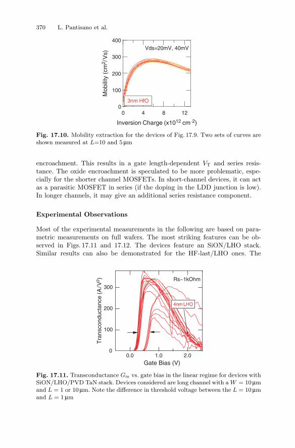
370 L. Pantisano et al.
400
300
200
100
0M
obili
ty (
cm2 /
Vs)
12840
Inversion Charge (x1012 cm−2)
Vds=20mV, 40mV
3nm HfO
Fig. 17.10. Mobility extraction for the devices of Fig. 17.9. Two sets of curves areshown measured at L=10 and 5 µm
encroachment. This results in a gate length-dependent VT and series resis-tance. The oxide encroachment is speculated to be more problematic, espe-cially for the shorter channel MOSFETs. In short-channel devices, it can actas a parasitic MOSFET in series (if the doping in the LDD junction is low).In longer channels, it may give an additional series resistance component.
Experimental Observations
Most of the experimental measurements in the following are based on para-metric measurements on full wafers. The most striking features can be ob-served in Figs. 17.11 and 17.12. The devices feature an SiON/LHO stack.Similar results can also be demonstrated for the HF-last/LHO ones. The
300
200
100
0
Tra
nsco
nduc
tanc
e (A
/V2 )
2.01.00.0Gate Bias (V)
Rs~1kOhm
4nm LHO
Fig. 17.11. Transconductance Gm vs. gate bias in the linear regime for devices withSiON/LHO/PVD TaN stack. Devices considered are long channel with a W = 10 µmand L = 1 or 10 µm. Note the difference in threshold voltage between the L = 10 µmand L = 1 µm

17 Fabrication of MBE High-κ Mosfets 371
20
15
10
5
0
Cap
acita
nce
(fF
/m2 )
2.01.00.0
Gate Bias (V)
consistent with Id-Vg
L=1umL=10um
4nm LHO
5nm LHO
6nm LHO
Fig. 17.12. Gate-to-channel capacitance Cgc vs. gate bias for the devices ofFig. 17.11 (SiON/LHO/PVD TaN stack). Devices considered are long channel witha W = 10 µm and L = 1 or 10 µm. Note the difference in threshold voltage betweenthe L = 10 µm and L = 1 µm
unoptimized process flow gives a length-dependent threshold voltage whichdiffers significantly from square devices to the ones with W/L = 10/1. Thiseffect precludes any series resistance extraction as well as mobility extrac-tion. Furthermore, despite the difficulty to measure the Cgc, in 10× 1 devicesof Fig. 17.12, it seems that the total CET is lower for short devices com-pared to long ones. This is consistent with (a) the poor Gm performanceobserved in Fig. 17.11 and (b) with the oxide regrowth in the TEM analysis(see Fig. 17.3).
17.3.5 Performance Comparison of MBE Materials WithALD in the ASAP Flow
Despite all the troubles and the issues linked with the processing of MBEmaterials, good performances were obtained in terms of leakage and MOSFETGm. In Fig. 17.13 the leakage at operating conditions (JG@VT + 1) is plottedas a function of the normalized Gm for all the long-channel samples considered.Two facts are of great importance in Fig. 17.13:
– For a given EOT the leakage for MBE samples is always lower than theirALD counterpart. As a tentative explanation the impurities content in theMBE film is lower.
– Normalized Gm (and thus the mobility) is higher for the MBE HfO2 com-pared to the ALD case (for similar EOT). This may have many causes.However it may be due to the (HfO2-thickness dependent) interfacial layercomposition changes during junction activation anneal. Similar high elec-tron mobilities were found also in PVD-deposited materials, as recentlyreported by Lee et al. [6].

372 L. Pantisano et al.
1.E−10
1.E−08
1.E−06
1.E−04
1.E−02
1.E+00
1.E+02
0 100 200 300 400 500 600
Linear Gm [uA/V2]
Leak
age
Cur
rent
[A/c
m² ]
SiON/LaHfOHf-Last/LaHfOHF-Last/HfO2ALD HfO2 mg030343
mgp030342SiO2
open: MBEclosed: ALD
1.5nm HfO2
open: MBE
closed: ALD
Fig. 17.13. High-κ performance plot chart featuring a comparison between the nor-malized transconductance and the gate current at operating conditions JG@VT + 1.The dashed line represents the SiON/poly-Si samples. ALD HfO2/PVD TaN samplesare shown. Experimental points with HfO2/poly-Si are also shown for comparison.Conversely from Table 17.1 and Fig. 17.9, for the sake of simplicity in this plot theseries resistance has been kept at zero
17.3.6 Threshold Voltage Instability
The threshold voltage instability has been measured using the pulsed tech-nique described in [7]. The transient ID-VG traces are shown in Fig. 17.14. Notethat these measurements were collected in 100 µs time range. The thresh-old voltage instability seems of little concern for LHO compared to HfO2
(Fig. 17.15).
17.4 Conclusions
For the first time transistor results on Lanthanum Hafnium Oxide (LHO)deposited by MBE are presented. The results for reference HfO2 deposited inthe same MBE tool are comparable to standard ALD HfO2.
Long-channel LHO devices exhibit reasonably good performance with mo-bility comparable to the HfO2 ones and featuring a much lower leakage. Short-channel devices are sensitive to some process issues linked to the etchingscheme considered. Similar to other amorphous high-κ layers, LHO devicesexhibit excellent leakage and minimal Vt-instability compared to HfO2.

17 Fabrication of MBE High-κ Mosfets 373
−1.0 −0.5 0.0 0.5 1.0 1.5 2.0 2.50.0
0.5
1.0
1.5
2.0
2.5
3.0
0.90 0.95 1.00 1.05 1.10 1.15 1.200.5
1.0
1.5
2.0
mg04041 W05
5nm LaHfO/TaN
Dra
in C
urre
nt I d
[µA
/m]
Gate Voltage Vg [V]
Id1 Id2 Id3 Id4 Id5
Dra
in C
urre
ntI d
[A/m
]
Gate Voltage Vg [V]
Fig. 17.14. Fast ID-VG traces for 5 nm LHO. The total measurement time is in theorder of few 100 µs
Acknowledgments
M. Claes, M. Demand, M. Houssa, M. Aoulaiche, G. Lujan, L-A. Ragnarsson,E. Rohr from IMEC are gratefully acknowledged for processing and charac-terization support. A. Guiller, H. Siegwart, D. Caimi, D. Webb, C. Rossel,and R. Germann from IBM are gratefully acknowledged for processing andcharacterization support. A. Dimoulas (NCSR “Democritos,” Athens, Greece)
1.0 1.2 1.4 1.6 1.8 2.0−100
−50
0
50
100
150
200
Shi
ft∆V
T [m
V]
Max. Gate Voltage Vg [V]
SiON/LaHfO 4nm 5nm 6nmHF-Last/LaHfO 4nm 5nm 6nmHF-Last/HfO2 4nm
Fig. 17.15. Summary of experimental findings for all the MBE layers consideredso far. The total measurement time is in the order of few 100 µs

374 L. Pantisano et al.
is acknowledged for discussion and support. These results were collected inthe framework of the European Project INVEST.
References
1. Many papers in recent International Electron devices meeting and VLSI sym-posium deal with the high-k integration. For a recent review see High-κ GateDielectrics (ed. by M. Houssa, IOP, London, 2003)
2. G.D. Wilk, R.M. Wallace, and J.M. Anthony, “High-k Gate Dielectrics: CurrentStatus and Materials Properties Considerations”, J. Appl. Phys., 89 5243 (2001)
3. D.A. Buchanan, E.P. Gusev, E. Cartier, et al., “80 nm Poly-Silicon Gatedn-FETs with Ultra-Thin Al 203 Gate Dielectric for ULSI Applications,” IEDMTech. Dig., 223–226 (2000)
4. J.W. Seo, J. Fompeyrine, A. Guiller, G. Norga, C. Marchiori, H. Siegwart, andJ.-P. Locquet, Appl. Phys. Lett., 83, 5211 (2003) and A. Dimoulas, G. Vellianitis,G. Mavrou, G. Apostopoulos, A. Travlos, C. Wiemer, M. Fanciulli, and Z.M.Rittersma, Appl. Phys. Lett. 85, 3205 (2004)
5. T. Schram, S. Beckx, S. De Gendt, J. Vertommen, and S. Lee, Solid State Tech.,61–64 (2003)
6. J.C. Lee, High-k dielectrics and MOSFET characteristics, IEDM, 95–98, 20037. A. Kerber, E. Cartier, L. Pantisano, M. Rosmeulen, R. Degraeve, T. Kauerauf,
G. Groeseneken, H.E. Maes, U. Schwalke, Int. Rel. Phys. Symp., (IEEE, NJ,2003), 41–45

Index
AC inversion capacitance, 118
Activation annealing, 349
Al2O3/Ge capacitor fabrication, 149
Al2O3 dielectrics, 140
Al2O3/AlGaN/GaN heterojunction,355
Al/Al2O3/Ge capacitors
charge trapping measurements for,154
electrical characterization of, 152–154
high-frequency C–V characteristicsfor, 153
leakage current density characteristicsof, 154
Al/HfO2/Ge capacitors
electrical characterization of, 155–159
surface nitridation of, 156
ALD reactor, 346
ALD-HfO2/Ge devices, degradation ofinterface quality of, 119
ALD-grown Al2O3
C–V characteristics, 249
electrical characterization of, 346
leakage current, 249
MOS diode, fabrication of, 249
structure and composition, 246
AlN surface passivation, 135–137
Aluminium–phosphorus oxide mixture,140
Amorphous silica, 280
Amorphous zirconia
dielectric intensity, 282
IR spectrum, 276
number of atoms, 282Angle-resolved XPS analysis, 129Annealing, 234Anodic etching method, 92Atomic force microscopy (AFM), 23,
33, 142, 237, 299Atomic layer chemical vapor deposition
(ALCVD), 149Atomic layer deposition (ALD), 183,
301, 316, 342HfO2 film, deposition of
Bragg–Brentano analysis, 188, 190characterization of, 188, 189epitaxial growth, 189–192grazing incidence, 186interfacial layer (IL) development,
187–189properties, 187
Lu2O3 film, deposition, 192–194Atomic-beam deposition
system, 143technique, 150, 151
Atomistic simulations, 166Attenuated total reflectance Fourier
transform infrared (ATR/FT-IR)spectrometry, 36
Auger Electron Spectroscopy (AES),75, 142
Ballistic electron emission microscopy(BEEM), 185
Ballistic ratios, on channels, 297Band offset engineering, 175–178Band-to-band tunneling, 318

376 Index
Bi-axial tensile strain, 7films, 11for enhancing hole mobility, 7
Bipolar electrochemical etching (BEE)technique, 92
Bixbyite lutetia, 274, 275Bonded SOI (BSOI), 53Born charges, 271, 279Borosilicate glass (BSG) film, 310Bragg–Brentano analysis, of HfO2 film,
188Brillouin zone center, 270Bulk strained fabrication of, 49Buried oxide (BOX), 48
C–V hysteresisperformance of, 117reduction of, 159
CET-Jg characteristics, 117Chain-to-chain interaction, 104Channel mobility, 352Charge carrier mobility, 43–45Charge modulation, 351Charge pumping measurement, 132Charge trapping characterization, 134Chemical vapor deposition (CVD), 217,
363Chemical–mechanical polishing (CMP),
298Clausius–Mossotti relation, 286CMOS
gate insulators for, 140integration processes and architec-
tures, 44scaling of
challenges, 293–294channel materials, 295–297drive current saturation, 295Ge vs Si, 296Monte Carlo simulations, 297power dissipation and gate length,
294transistor channels, 48
CMOSFET, performances of, 11560Coγ-irradiation, 215Conduction band offset (CBO), 121,
199Coulomb interactions, 75Coulomb scattering, 355
Covalently bonded material, 174Croce–Nevot factor, 185Cross-sectional transmission electron
microscopy (XTEM), 146Crystal Originated Particles (COP), 63CVD deposition process, 126
Dangling bond (DB) defects, 214Defect density and stoichiometric ratio,
353Deionized (DI) water, 80, 84, 142Density functional theory, 166DHF-cleaned germanium substrates,
122Diels–Alder reaction, 101Dimer antibonding states, 173Direct tunneling current, 346Double-gate (DG) FET, 294, 296Drain current density, 352, 354Drain current drift, 343Drain current hysteresis, 343Dual gate-MOSFETs, 22
Electron energy loss spectroscopy(EELS), 142
Electron injection barrier, 175, 178Electron mobility degradation, 44Electron spectroscopy for chemical
analysis (ESCA), 74Electron spin resonance (ESR)
point defects, identification of, 216Si/high-κ insulator studies, 215
Electron traps, 134Electron-beam deposition, 354Electron-beam evaporation, 151Electronic noise measurement, 28Electronically saturated interface
structure, 175Electropositive elements, 170Enthalpies of formation, 345Epitaxial crystallization, 118Equivalent oxide thickness (EOT), 140,
153, 155, 230, 263, 300, 309, 317
Fermi level pinning, 342Fermi surface pinning, 232Fermi-level unpinning, 229, 232, 253FLASH memories, 288Flat band voltage, 153

Index 377
Flat single crystal germanium surfaces,wet chemical treatment of, 83–89
Fourier-transform infrared (FTIR)spectroscopy, 73, 75, 77, 100, 105
Fully depleted sSOI (FDsSOI) devices,60
Ga2O3(Gd2O3) gate oxide and GaASand MOS diodes, 232–236dielectric films, 241leakage currents, 238–240single crystal, 239–241thermodynamic stability of, 236–239
GaASbinary oxide dielectrics for, 233film deposition, using ALD, 183high-κ dielectrics for
ALD-grown Al2O3 as, 246–250deposition, 182–183electrical properties, 197Ga2O3(Gd2O3), 232–246
GaAs MOS capacitors, 348GaAs MOSFETs, 231, 236
depletion-mode, 243–246enhancement mode, 242fabrication and characterization of,
349–352GaN MOS-HEMT, fabrication and
characterization of, 353–356GaN MOSFET’s, 230, 231
Gd2O3 growth, 250–251RHEED patterns, 251surface passivation, 252
Gas phase oxidation, 105Gas source molecular beam epitaxy
(GSMBE), 237Gate dielectrics, 353Gate insulator, 139Gate leakage current, 130, 341, 350, 353Gate stack
capacitance, 346structures, 345
gate tunnelling current, 1Gd2O3 film, 182Ge buried Channel MOSFETs, 319
carrier ratio, 322doping profile, 321gate dielectric, 322–323material growth, 321–322
PMOSFET fabricationcharacteristics of, 327–329CMOS structure, 325s-Ge layer growth, 325“TM Ge”, 326–328“UHV Ge”, 328–329
scaling concern, 320, 321Si cap thickness, 321strain measurement, 322
Ge condensation effect, 52Ge MOS capacitors
capacitor fabrication process, 149surface nitridation, effect of, 147–149
Ge MOSFETsburied channel, 321–329investigate using gate dielectrics, 116Monte Carlo simulations, 297n-MOSFET fabrication, 307
output characteristics, 309self-aligned gate-last process,
308–310p-MOSFET fabrication, 306
effective hole mobility, 307gate leakage, 307sub-400C process, 306
surface channel, 316–319Ge oxynitride (GeOxNy), 316Ge pMOS transistor, 334Ge surface channel MOSFETs
C–V characteristics, 319band-to-band tunneling, 318dopant diffusion, 317–319gate dielectric, 316HfO2 deposition, 318nitrogen passivation, 317surface preparation, 316–317
Ge surface passivation, 118Ge-channel MOSFETs, 140Germanium (Ge)
dopant activation, 336–337film deposition, using ALD, 183, 302gate stack passivation
channel mobility values, 336Si layer growth, 335
heteroepitaxial growth on Sichallenges, 298–299CVD growth, 299hydrogen annealing, 299lattice-mismatch, 298

378 Index
HfO2 film depositionC–V characteristics, 263film thickness, Ge vs Si, 259MIS capacitors, characteristics, 265surface orientation, effects of,
261–262TEM micrographs, 260
high-κ dielectricsdeposition, 181–182, 194–197electrical properties, 194–198
ion implantation doping, 304nanoscale gate stacks on, 300
dielectric leakages, 302, 303high-permittivity dielectrics,
300–301oxynitride dielectrics, 300
properties of, 213solid source doping, 305Y2O3 MIS capacitorsC–V characteristics, 263, 264capacitance characteristics, 266SIMS profiles, 266TEM micrograph, 263Zerbst plot, 264, 266
Germanium nanowires, 102, 103Germanium On Insulator (GOI)
substrates, 337–338buried insulator, 63devices fabricated characteristics, 338fabrication of, 63introduction to, 60–61manufacturing routes, 61–62validations at device level, 64
Germanium oxynitride dielectrics, 300Germanium quantum dots, 103Germanium surfaces
alkylation of hydrogen terminated,104
chlorine passivation of, 99–101hydrogenation of, 83–84methods for cleaning, 74, 141–144nitridation and oxynitridation of,
93–97organic molecules as passivating
agent of, 101–103oxidation of, 76sulfur passivation of, 97–98surface characterization, 73surface passivation, 73
wet chemical pretreatment for, 76wet chemical treatment of, 83–89
Germanium wafers, 142, 151Germinate (MeGexOY ), 316Gibbs energy, 345Glazing incidence X-ray reflectivity
(GIXR), 258Global strain, 49–51Global strain Si MOSFETs, advantages
of, 12Global strain technology, 11Grignard reagents, 104
H-passivation, degree of, 105Hall measurement, 355HEMT technologies, 230Heteroepitaxy, 297Hf–germanide bonds, formation of, 119HF-etched substrates, 346Hf-silicate, nitride based, 212HfO2 Ge MOS capacitor, J–V
characteristics of, 127HfO2/Ge capacitor fabrication, 149–151High κ MOS capacitor, 234High band to band tunneling (BTBT),
295High Coulomb scattering rate, 230High electron mobility transistors
(HEMTs), 243, 341High frequency inversion C–V , 120High mobility semiconductor layers, 66High-κ dielectrics
agglomeration, degree of, 344band offset measurement, 198–200barrier energies, determination of,
185–186characterization techniques, 184–185deposition methods, 116, 128, 182electrical properties of, 194–198for Ge based devices, 181–182on GaAs, 182–183properties of, 269stack structure, determination of, 184
High-κ gate dielectrics, 343High-k Ge MOSFETs, 134High-k oxides
deposition of metal ions, 168electrically inactive interface, 175growth of, 165, 168

Index 379
High-k/GaAs gate stacks, 343High-k/Ge system
development of, 116epitaxial growth of, 118interface quality of, 116, 118issues and requirements for, 117surface nitridation of, 122technological progress in, 115use of, 140
High-intrinsic carrier concentration, 120High-resolution transmission electron
microscopy (HRTEM), 237High-temperature anneal treatment,
150Hole mobility enhancement factor, 7Hybrid orientation technology (HOT),
47Hydrofluoric (HF) acid treatment, 83Hydrogen annealing, 299Hydrogermylation reaction, 103Hysteresis loop voltage, 236
Inductive coupled plasma Augerelectron spectroscope (ICP-AES),23
Inelastic mean free path (IMFP), 129InGaAs MOSFETs
fabrication and characterization,352–353
inversion-channel, 243Inter-band scattering, suppression of, 11Inter-valley scattering, suppression of, 5Interdiffused interface, 155Interface roughness, scattering, 355Interface state density, 115, 153, 158Interface trap density Dit, 24, 149, 231,
233, 235, 343Interfacial dislocation, 118Interfacial layer formation, 141, 146Internal photoemission spectroscopy
(IPE), 183, 198International Technology Roadmap for
Semiconductors (ITRS), 211, 293Inversion-layer
holes, transport properties of, 11subband energy splitting, effect of, 5
Ion implantation doping, on Ge, 304Ion intensity ratio, 146Ion-induced defects, 142
Ion-sputtering-induced roughening, 76Ionic crystal, 174Island formation of, 298Isopropyl alcohol (IPA), 33Isotropic oxidation, 26
K-band spectrometer, 216Kohn–Sham DFT approach, 272
La2Hf2O7 (LHO) devices, fabricationof, 364
Langmuir isotherm model, 104Lanthanum aluminate (LaAlO3)
alloys, 285amorphous
dielectric intensities, 283, 284radial distribution functions, 283
IR spectrum, 279predictions about, 277Raman modes, 278
Lanthanum Hafnium Oxide (LHO), 372Lanthanum, adsorption of, 173Large area capacitors, 366Layer transfer techniques, Ge Donor
substrate for, 53, 62–63Leakage current
characteristics, 121density, 158, 346, 348
Linear response theory, in high k oxides,270–272
Local density approximation (LDA), 98Local strain evaluation techniques, 14Local strain technology for MOSFETs,
13Local thermal mixing (LTM), 325, 327Lock-in amplifier, 351Long-channel LHO devices, 372Long-channel MOSFET, 367Longitudinal optical (LO) phonon
modes, 75, 82, 272Low energy ion scattering (LEIS), 184Low-leakage gate stacks, 141Low-pressure chemical vapor deposition
(LPCVD), 149, 305, 308Low-temperature oxide (LTO) gate, 141LSI devices, integration and perfor-
mance of, 21
Materials research, computationalapproach for, 166

380 Index
Medium-energy ion scattering (MEIS)analysis, 126, 151, 325, 345
MEIS spectra, 233Metal gate electrode, 309Metal organic chemical vapor deposition
(MOCVD), 144, 182, 220, 316Metal work function, 348Metal-Gated Germanium MOSFET
processes, 306–310Metal-organic precursor, 125Metal-semiconductor field-effect-
transistor (MESFET), 341Microwave network analyzer, 351Microwave-exited high-density plasma
oxidation, 22–24Midgap bulk semiconductor traps, 116MIS capacitors, 257, 259MOCVD HfO2 deposition, 136Molecular beam deposition of HfO2, 146Molecular beam epitaxy (MBE), 150,
168, 182, 298, 342, 364Molecular dynamics simulations, 165Monte Carlo (DAMOCLESTM)
simulations, of Ge MOSFET, 297Moore’s law, 61, 211MOS capacitor
C–V measurements of, 118characteristics of, 126–127Tungsten-gated, 300
MOS channelscarrier velocity in, 2local strain technology for, 13
MOS diode, 236C–V curves, 234leakage current density curve, 233
MOS fabrication, 141MOSFET
BTI characteristics of, 133channel mobility of, 139charge trapping in, 133device characterization, 365drive current capability of, 115fabrication, 234, 236GaAs-based, 341Ge-channel, 140high performance (HP), 130high-k deposition, 129high-k Ge, 115long-channel, 367
low operation power (LOP), 130miniaturization of, 21noise characteristics of, 28static characteristics of, 24
Multiple gate transistors, 59Multiple Hydrogen Annealing for
Heteroepitaxy (MHAH), 299Multiple internal reflection (MIR)
spectroscopy, 75
n-Channel MOSFETsdependence of electron mobility in, 6mobility enhancement in, 3–6
Native oxide passivation layer, 142NBTI degradation, 134Near-infrared photo-detectors, 61Nitride interfacial layer, 126NMOS transistors, 47, 49, 60Nonuniform interfacial layer, 126
Optical band gap, 115Optical phonon modes, 82Organometallic reagents, 104Oxide band structure, 176Oxide–semiconductor interfaces, 355Oxygen implantation, 349
Pb-type centers, 214, 223p-Channel MOSFETs, mobility
enhancement in, 7–10p-MOS capacitors, gate leakage currents
of, 130p-MOSFETs
electron mobility in, 128hole mobility of, 127I d–Vd characteristics of, 25, 127
Partially depleted (PD) transistors, 51Phonon eigenvector, 271Phonon scattering, 6, 355Phospho-silicate glass (PSG), 305Phosphorus (P), as Ge dopant, 336Photoresist, 306, 309, 349Physical vapor deposition (PVD), 363Piezo-resistance effect, 5Pinch-off voltage, 349, 352Plasma-PH3 surface passivation,
135–137Plasma-enhanced nitridation technique,
96

Index 381
Plasma-enhanced-chemical-vapor-deposition (PECVD), 353
PMOS transistors, 47, 49Point defects, in high-κ metal oxides
ESR measurementsK-band ESR spectra, 221, 222
experimental studiescapacitance-voltage curves, 218electrical analysis, 217–220interface trap density, 219
identification using ESR, 216sample studied, 217
Porous germanium substrate, elec-trochemical hydrogenation of,91
Postdeposition annealing (PDA), 125,132, 144, 146, 213, 217
Postmetal annealing, thermal stabilityof, 131
Power-added efficiency (PAE), 350Pseudomorphic HEMTs (p-HEMTs),
352Pt-gated Ge n-MOSFETs, 309Pt-gated MOS capacitors, 301
Quantum confinement effects, 127Quantum mechanics, theorems of, 166Quantum yield (Y ) spectra, 186Quantum-mechanical effects, 159Quantum-mechanical leakage currents,
165Quasi-ballistic transport models, 2Quasi-ionic interaction, 175
Radio frequency (RF) discharge sources,150
Raman modes, 276–278Raman spectroscopy, 57, 77Rapid thermal annealing, 58, 141, 346Rapid thermal oxidation (RTO), 316Rapid thermal processing (RTP), 305,
309Rare-earth aluminates, 277–279Reflection high-energy electron diffrac-
tion (RHEED), 142, 173, 237,239
Reoxidation/hydrocarbon insertion, 101Residual surface oxygen, 143Rietveld refinement, 185
S-parameter network analyzer, 350Scanning tunneling microscopy (STM),
23, 73, 76, 83Scanning tunneling spectroscopy (STS),
76Schottky barrier, 243, 341, 348, 353Schottky plot, 199, 200Second harmonic generation (SHG), 84,
99Semi-insulating GaAs substrates, 341Semiconductor epi-layer growth, 349Semiconductor Industry Association
(SIA), 211semiconductor surfaces, reconstruction
of, 135Semiconductor–semiconductor interface,
355Series resistance extraction, 371Sesquioxides, 274SGOI
architectures, 55short channel devices, 60
Shallow trench isolation (STI), 49Sheet carrier density, 354Short-channel
devices, 372effects, 2
Short-circuit current-gain cut-offfrequency, 350
Si CMOS scaling, 230, 293Si interlayer passivation, 133Si MOS capacitor, 324Si MOSFETs, piezo-resistance effect on,
5Si p-channel MOSFETs, dependence of
hole mobility in, 8Si(001) surface
atomic and electronic topology of,170
chemical bonding in, 174metal adsorption on, 168–174Zintl–Klemm concept to, 170
Si(110) surfacecrystalline orientations for bulk
substrates, 44hydrogen termination of, 35–38suppressed of microroughness on, 27
Si-oxynitride, 212SiGe Layer On Insulator (SGOI), 51

382 Index
Silane surface passivation, 128Silicon crystalline orientations
for bulk substrates, 44for SOI substrates, 45
Silicon dimer, 171, 176silicon passivation (SP), 128Silicon substrate, chemistry of, 167–168Silicon surface orientation, 24Silicon-on-insulator (SOI), 342
architectures, 48, 66materials, applications of, 43substrates, 337wafers
fabrication of, 45, 48strained, 48
SIMOX technology, 52, 57SiO2 gate dielectric formation, 158Solid-state transformation, 173Source/drain dopants, 131Split-CV measurement, 132SrTiO3 and Si(001), interface of,
174–175sSOI wafers, 59Stanford Nanofabrication Facility
(SNF), 309Strain-application techniques, 14Strain-induced energy, 10Strained Si on Insulator (sSOI), 51,
57–60Strained-Si CMOS technology
impact of mobility Enhancement on,2–3
performance enhancement in, 1principle and the device application
of, 2Strained-Si-directly-On-Insulator
(SSDOI) MOSFETs, 11Strained-Si-On-Insulator (Strained-SOI)
MOSFETs, 11“Stranski–Krastanow” (S–K) growth,
298Surface microroughness
degradation of, 32evaluation of, 23for improving of current drivability,
29in ultrapure Water, 31–33suppression by IPA/UPW Solution,
33
Surface nitridationeffect of, 124–125for reducing leakage current density,
153Surface passivation layer, 141Surface preparation techniques, 146Surface pretreatment with NH3,
144–149Surface roughness scattering, probabil-
ity of, 7Surface silicon passivation, 128
Tetrakis-diethylaminohafnium, 220, 221Thermal annealing, 58, 124Thermal desorption spectroscopy
(TDS), 35Thermally activated hydrogermylation,
103Thermodynamic instability, of Ge oxide,
116Threshold voltage instability, 372time-of-flight secondary ion mass
spectrometry (TOF-SIMS), 144Transistor channel mobility, 43Transition-metal
aluminates, 277–279dioxides, 273–274
Transmission electron microscopy(TEM), 184, 246, 258, 299
Transmission line method (TLM), 355,356
Transverse optical (TO) phonon modes,75, 82, 272
Trap density Ge/HfO2 interface,219–220
Trapped charge density, 154Tungsten-gated MOS capacitors, 300Tunneling leakage current, 120, 212
UHV/MBE system, 232ULSI devices, leakage current in, 21Ultra-high vacuum (UHV) environment,
74, 79, 105Ultrahigh vacuum annealing, 142Ultrahigh vacuum chemical-vapor-
deposition (UHVCVD), 298Ultrathin films, microscopic screening,
287interface model, 288

Index 383
phonon modes, 288polarization, change in, 288–289
Uni-axial compressive strain, 7, 10, 13Uni-axial mechanical strain, 8UV micro-Raman, 59UV ozone oxidation, 141, 151UV/corona ion charging, 215
Valence band offset (VBO), 121, 135,176, 199
velocity saturation effect, 2Voltage drain stress, 356
W/HfO2/Ge capacitors electricalcharacterization of, 155–159
Wafer bonding interface, 48Wafer fabrication, deviation in, 46Wet chemical
etching, 142methods, 74, 140pretreatment, 76
X-ray absorption near edge spectroscopy(XANES), 100
X-ray diffraction (XRD), 184, 185, 299X-ray photoelectron spectroscopy
(XPS), 73, 142, 247, 248, 258X-ray photoemission spectroscopy
(XPS), 74, 301X-ray reflectivity (XRR), 184
application of, 184experimenital setup, 185
XSAM-800 spectrometer, 185
Yttria, IR spectra, 276
Ziconia (ZrO2), dielectric intensity, 273Zintl–Klemm concept, 171, 173Zirconium silicates, 286
ab initio studies, 286dielectric constant calculation,
286–288