snx4hc138 3-line to 8-line decoders/demultiplexers
TRANSCRIPT

SNx4HC138 3-Line To 8-Line Decoders/Demultiplexers
1 Features• Targeted Specifically for High-Speed Memory
Decoders and Data-Transmission Systems• Wide Operating Voltage Range (2 V to 6 V)• Outputs Can Drive Up To 10 LSTTL Loads• Low Power Consumption, 80-µA Maximum ICC• Typical tpd = 15 ns• ±4-mA Output Drive at 5 V• Low Input Current of 1-µA Maximum• Active Low Outputs ( Selected Output is Low)• Incorporate Three Enable Inputs to Simplify
Cascading or Data Reception
2 Applications• LED Displays• Servers• White Goods• Power Infrastructure• Building Automation• Factory Automation
3 DescriptionThe SNx4HC138 devices are designed to be used in high-performance memory-decoding or data-routing applications requiring very short propagation delay times. In high-performance memory systems, these decoders can be used to minimize the effects of system decoding. When employed with high-speed memories using a fast enable circuit, the delay times of these decoders and the enable time of the memory are usually less than the typical access time of the memory. This means that the effective system delay introduced by the decoders is negligible.
Device InformationPART NUMBER PACKAGE(1) BODY SIZE (NOM)
SN74HC138D SOIC (16) 9.90 mm x 3.90 mm
SN74HC138DB SSOP (16) 6.20 mm x 5.30 mm
SN74HC138N PDIP (16) 19.32 mm x 6.35 mm
SN74HC138NS SO (16) 10.20 mm x 5.30 mm
SN74HC138PW TSSOP (16) 5.00 mm x 4.40 mm
SN54HC138J CDIP (16) 21.34 mm x 6.92 mm
SN54HC138W CFP (16) 10.16 mm x 6.73 mm
SN54HC138FK LCCC (20) 8.89 mm x 8.89 mm
(1) For all available packages, see the orderable addendum at the end of the data sheet.
Pin numbers shown are for the D, DB, J, N, NS, PW, and W packages.
Functional Block DIagram
SN54HC138, SN74HC138SCLS107G – DECEMBER 1982 – REVISED OCTOBER 2021
An IMPORTANT NOTICE at the end of this data sheet addresses availability, warranty, changes, use in safety-critical applications, intellectual property matters and other important disclaimers. PRODUCTION DATA.

Table of Contents1 Features............................................................................12 Applications..................................................................... 13 Description.......................................................................14 Revision History.............................................................. 25 Pin Configuration and Functions...................................3
Pin Functions.................................................................... 36 Specifications.................................................................. 4
6.1 Absolute Maximum Ratings........................................ 46.2 ESD Ratings: SN74HC138......................................... 46.3 Recommended Operating Conditions.........................46.4 Thermal Information: SN74HC138..............................56.5 Thermal Information: SN54HC138..............................56.6 Electrical Characteristics.............................................56.7 Electrical Characteristics: SN74HC138...................... 66.8 Electrical Characteristics: SN54HC138...................... 66.9 Switching Characteristics............................................66.10 Switching Characteristics: SN74HC138....................76.11 Switching Characteristics: SN54HC138....................76.12 Typical Characteristic................................................7
7 Parameter Measurement Information............................ 88 Detailed Description........................................................9
8.1 Overview..................................................................... 98.2 Functional Block Diagram........................................... 98.3 Feature Description.....................................................98.4 Device Functional Modes..........................................10
9 Application and Implementation.................................. 119.1 Application Information..............................................119.2 Typical Application.................................................... 11
10 Power Supply Recommendations..............................1211 Layout...........................................................................12
11.1 Layout Guidelines................................................... 1211.2 Layout Example...................................................... 12
12 Device and Documentation Support..........................1312.1 Documentation Support.......................................... 1312.2 Related Links.......................................................... 1312.3 Receiving Notification of Documentation Updates..1312.4 Support Resources................................................. 1312.5 Trademarks.............................................................1312.6 Electrostatic Discharge Caution..............................1312.7 Glossary..................................................................13
13 Mechanical, Packaging, and Orderable Information.................................................................... 13
4 Revision HistoryNOTE: Page numbers for previous revisions may differ from page numbers in the current version.
Changes from Revision E (September 2003) to Revision F (September 2016) Page• Added ESD Ratings table, Feature Description section, Device Functional Modes, Application and
Implementation section, Power Supply Recommendations section, Layout section, Device and Documentation Support section, and Mechanical, Packaging, and Orderable Information section................... 1
• Deleted Ordering Information table; see POA at the end of the data sheet....................................................... 1• Changed RθJA values from 73 to 87.3 (D), from 82 to 104.3 (DB), from 67 to 54.8 (N), from 64 to 91.1 (NS),
and from 108 to 114.6 (PW)................................................................................................................................5
Changes from Revision F (September 2016) to Revision G (October 2021) Page• Updated the ESD ratings table to fit modern data sheet standards....................................................................4
SN54HC138, SN74HC138SCLS107G – DECEMBER 1982 – REVISED OCTOBER 2021 www.ti.com
2 Submit Document Feedback Copyright © 2021 Texas Instruments Incorporated
Product Folder Links: SN54HC138 SN74HC138
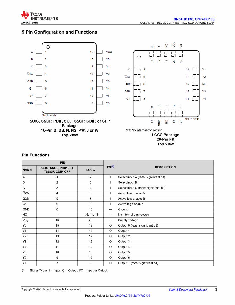
5 Pin Configuration and Functions
SOIC, SSOP, PDIP, SO, TSSOP, CDIP, or CFP Package
16-Pin D, DB, N, NS, PW, J or WTop View
NC: No internal connectionLCCC Package
20-Pin FKTop View
Pin FunctionsPIN
I/O(1) DESCRIPTIONNAME SOIC, SSOP, PDIP, SO,
TSSOP, CDIP, CFP LCCC
A 1 2 I Select input A (least significant bit)
B 2 3 I Select input B
C 3 4 I Select input C (most significant bit)
G2A 4 5 I Active low enable A
G2B 5 7 I Active low enable B
G1 6 8 I Active high enable
GND 8 10 — Ground
NC — 1, 6, 11, 16 — No internal connection
VCC 16 20 — Supply voltage
Y0 15 19 O Output 0 (least significant bit)
Y1 14 18 O Output 1
Y2 13 17 O Output 2
Y3 12 15 O Output 3
Y4 11 14 O Output 4
Y5 10 13 O Output 5
Y6 9 12 O Output 6
Y7 7 9 O Output 7 (most significant bit)
(1) Signal Types: I = Input, O = Output, I/O = Input or Output.
www.ti.comSN54HC138, SN74HC138
SCLS107G – DECEMBER 1982 – REVISED OCTOBER 2021
Copyright © 2021 Texas Instruments Incorporated Submit Document Feedback 3
Product Folder Links: SN54HC138 SN74HC138

6 Specifications6.1 Absolute Maximum Ratingsover operating free-air temperature range (unless otherwise noted)(1)
MIN MAX UNITVCC Supply voltage range –0.5 7 V
IIK Input clamp current(2) VI < 0 or VI > VCC ±20 mA
IOK Output clamp current(2) VO < 0 or VO > VCC ±20 mA
IO Continuous output current VO = 0 to VCC ±25 mA
Continuous current through VCC or GND ±50 mA
TJ Junction temperature 150 °C
Tstg Storage temperature –65 150 °C
(1) Stresses beyond those listed under Absolute Maximum Ratings may cause permanent damage to the device. These are stress ratings only, which do not imply functional operation of the device at these or any other conditions beyond those indicated under Recommended Operating Conditions. Exposure to absolute-maximum-rated conditions for extended periods may affect device reliability.
(2) The input and output voltage ratings may be exceeded if the input and output current ratings are observed.
6.2 ESD Ratings: SN74HC138VALUE UNIT
V(ESD) Electrostatic dischargeHuman-body model (HBM), per ANSI/ESDA/JEDEC JS-001(1) ±2000
VCharged device model (CDM), per ANSI/ESDA/JEDEC JS-002(2) ±1000
(1) JEDEC document JEP155 states that 500-V HBM allows safe manufacturing with a standard ESD control process.(2) JEDEC document JEP157 states that 250-V CDM allows safe manufacturing with a standard ESD control process.
6.3 Recommended Operating Conditionsover operating free-air temperature range (unless otherwise noted)(1)
MIN NOM MAX UNITVCC Supply voltage 2 5 6 V
VIH High-level input voltage
VCC = 2 V 1.5
VVCC = 4.5 V 3.15
VCC = 6 V 4.2
VIL Low-level input voltage
VCC = 2 V 0.5
VVCC = 4.5 V 1.35
VCC = 6 V 1.8
VI Input voltage 0 VCC V
VO Output voltage 0 VCC V
Δt/Δv Input transition rise or fall time
VCC = 2 V 1000
nsVCC = 4.5 V 500
VCC= 6 V 400
Cpd Power dissipation capacitance (no load) 85 pF
TA Operating free-air temperatureSN54HC138 –55 125
°CSN74HC138 –40 85
(1) All unused inputs of the device must be held at VCC or GND to ensure proper device operation. See TI application report, Implications of Slow or Floating CMOS Inputs (SCBA004).
SN54HC138, SN74HC138SCLS107G – DECEMBER 1982 – REVISED OCTOBER 2021 www.ti.com
4 Submit Document Feedback Copyright © 2021 Texas Instruments Incorporated
Product Folder Links: SN54HC138 SN74HC138

6.4 Thermal Information: SN74HC138
THERMAL METRIC(1)
SN74HC138UNITD (SOIC) DB (SSOP) N (PDIP) NS (SO) PW (TSSOP)
16 PINS 16 PINS 16 PINS 16 PINS 16 PINSRθJA Junction-to-ambient thermal resistance 87.3 104.3 54.8 91.1 141.6 °C/W
RθJC(top) Junction-to-case (top) thermal resistance 45.8 54.7 42.1 49.5 49.5 °C/W
RθJB Junction-to-board thermal resistance 44.8 54.9 34.8 51.5 59.6 °C/W
ψJT Junction-to-top characterization parameter 14.2 17.7 27 17.8 6.9 °C/W
ψJBJunction-to-board characterization parameter 44.5 54.4 34.7 51.2 59.1 °C/W
(1) For more information about traditional and new thermal metrics, see the Semiconductor and IC Package Thermal Metrics application report.
6.5 Thermal Information: SN54HC138
THERMAL METRIC(1)
SN54HC138(2)
UNITJ (CDIP) W (CFP) FK (LCCC)16 PINS 16 PINS 20 PINS
RθJA Junction-to-ambient thermal resistance — — — °C/W
RθJC(top) Junction-to-case (top) thermal resistance 45.4 68.1 49 °C/W
RθJB Junction-to-board thermal resistance — 118.4 47.7 °C/W
ψJT Junction-to-top characterization parameter — — 7.2 °C/W
ψJB Junction-to-board characterization parameter 62.5 — — °C/W
RθJC(bot) Junction-to-case (bottom) thermal resistance 17.7 9 — °C/W
(1) For more information about traditional and new thermal metrics, see the Semiconductor and IC Package Thermal Metrics application report.
(2) RθJC follows MIL-STD-883, and RθJB follows JESD51.
6.6 Electrical CharacteristicsTA = 25°C (unless otherwise noted)
PARAMETER TEST CONDITIONS MIN TYP MAX UNIT
VOH VI = VIH or VIL
IOH = –20 µA
VCC = 2 V 1.9 1.998
V
VCC = 4.5 V 4.4 4.499
VCC = 6 V 5.9 5.999
IOH = –4 mA, VCC = 4.5 V 3.98 4.3
IOH= –5.2 mA, VCC = 6 V 5.48 5.8
VOL VI= VIH or VIL
IOL = 20 µA
VCC = 2 V 0.002 0.1
V
VCC = 4.5 V 0.001 0.1
VCC = 6 V 0.001 0.1
IOL = 4 mA, VCC = 4.5 V 0.17 0.26
IOL = 5.2 mA, VCC = 6 V 0.15 0.26
II VI = VCC or 0, VCC = 6 V ±0.1 ±100 nA
ICC VI = VCC or 0, IO = 0, VCC = 6 V 8 µA
Ci VCC = 2 V to 6 V 3 10 pF
www.ti.comSN54HC138, SN74HC138
SCLS107G – DECEMBER 1982 – REVISED OCTOBER 2021
Copyright © 2021 Texas Instruments Incorporated Submit Document Feedback 5
Product Folder Links: SN54HC138 SN74HC138

6.7 Electrical Characteristics: SN74HC138over operating free-air temperature range (unless otherwise noted)
PARAMETER TEST CONDITIONS MIN TYP MAX UNIT
VOH VI = VIH or VIL
IOH = –20 µA
VCC = 2 V 1.9
V
VCC = 4.5 V 4.4
VCC = 6 V 5.9
IOH = –4 mA, VCC = 4.5 V 3.84
IOH= –5.2 mA, VCC = 6 V 5.34
VOL VI= VIH or VIL
IOL = 20 µA
VCC = 2 V 0.1
V
VCC = 4.5 V 0.1
VCC = 6 V 0.1
IOL = 4 mA, VCC = 4.5 V 0.33
IOL = 5.2 mA, VCC = 6 V 0.33
II VI = VCC or 0, VCC = 6 V ±1000 nA
ICC VI = VCC or 0, IO = 0, VCC = 6 V 80 µA
Ci VCC = 2 V to 6 V 10 pF
6.8 Electrical Characteristics: SN54HC138over operating free-air temperature range (unless otherwise noted)
PARAMETER TEST CONDITIONS VCC MIN TYP MAX UNIT
VOH VI = VIH or VIL
IOH = –20 µA
VCC = 2 V 1.9
V
VCC = 4.5 V 4.4
VCC = 6 V 5.9
IOH = –4 mA, VCC = 4.5 V 3.7
IOH= –5.2 mA, VCC = 6 V 5.2
VOL VI= VIH or VIL
IOL = 20 µA
VCC = 2 V 0.1
V
VCC = 4.5 V 0.1
VCC = 6 V 0.1
IOL = 4 mA, VCC = 4.5 V 0.4
IOL = 5.2 mA, VCC = 6 V 0.4
II VI = VCC or 0, VCC = 6 V ±1000 nA
ICC VI = VCC or 0, IO = 0, VCC = 6 V 160 µA
Ci VCC = 2 V to 6 V 10 pF
6.9 Switching CharacteristicsTA = 25°C and CL = 50 pF (unless otherwise noted; see Section 7)
PARAMETER TEST CONDITIONS MIN TYP MAX UNIT
tpd
From A, B, or C (input) to any Y (output)
VCC = 2 V 67 180
ns
VCC = 4.5 V 18 36
VCC = 6 V 15 31
From enable (input) to any Y (output)
VCC = 2 V 66 155
VCC = 4.5 V 18 31
VCC = 6 V 15 26
tt To any output
VCC = 2 V 38 75
nsVCC = 4.5 V 8 15
VCC = 6 V 6 13
SN54HC138, SN74HC138SCLS107G – DECEMBER 1982 – REVISED OCTOBER 2021 www.ti.com
6 Submit Document Feedback Copyright © 2021 Texas Instruments Incorporated
Product Folder Links: SN54HC138 SN74HC138

6.10 Switching Characteristics: SN74HC138over recommended operating free-air temperature range and CL = 50 pF (unless otherwise noted; see Section 7)
PARAMETER TEST CONDITIONS MIN TYP MAX UNIT
tpd
From A, B, or C (input) to any Y (output)
VCC = 2 V 225
ns
VCC = 4.5 V 45
VCC = 6 V 38
From enable (input) to any Y (output)
VCC = 2 V 195
VCC = 4.5 V 39
VCC = 6 V 33
tt To any output
VCC = 2 V 95
nsVCC = 4.5 V 19
VCC = 6 V 16
6.11 Switching Characteristics: SN54HC138over recommended operating free-air temperature range and CL = 50 pF (unless otherwise noted; see Section 7)
PARAMETER TEST CONDITIONS MIN TYP MAX UNIT
tpd
From A, B, or C (input) to any Y (output)
VCC = 2 V 270
ns
VCC = 4.5 V 54
VCC = 6 V 46
From enable (input) to any Y (output)
VCC = 2 V 235
VCC = 4.5 V 47
VCC = 6 V 40
tt To any output
VCC = 2 V 110
nsVCC = 4.5 V 22
VCC = 6 V 19
6.12 Typical Characteristic
Supply Voltage VCC (V)
Pro
pa
ga
tio
n D
ela
y F
rom
A, B
, C
to
an
y Y
(n
s)
2 2.5 3 3.5 4 4.5 5 5.5 615
20
25
30
35
40
45
50
55
60
65
70
D001
Figure 6-1. Typical Propagation Delay vs Supply Voltage
www.ti.comSN54HC138, SN74HC138
SCLS107G – DECEMBER 1982 – REVISED OCTOBER 2021
Copyright © 2021 Texas Instruments Incorporated Submit Document Feedback 7
Product Folder Links: SN54HC138 SN74HC138

7 Parameter Measurement Information
VOLTAGE WAVEFORM
INPUT RISE AND FALL TIMES
50%50%10%10%
90% 90%VCC
0 V
tr t
Input
f
VOLTAGE WAVEFORMS
PROPAGATION DELAY AND OUTPUT TRANSITION TIMES
50%
50%50%10%10%
90% 90%
VCC
VOH
VOL
0 V
tr t
Input
f
In-Phase
Output
50%
tPLH tPHL
50% 50%10% 10%
90%90%VOH
VOL
tt rf
tPHL tPLH
Out-of-Phase
Output
Test
Point
From Output
Under Test
CL = 50 pF
(see Note A)
LOAD CIRCUIT
NOTES: A. CL includes probe and test-fixture capacitance.
B. Phase relationships between waveforms were chosen arbitrarily. All input pulses are supplied by generators having the following
characteristics: PRR ≤ 1 MHz, ZO = 50 Ω, tr = 6 ns, tf = 6 ns.
C. The outputs are measured one at a time with one input transition per measurement.
D. tPLH and tPHL are the same as tpd.
Figure 7-1. Load Circuit and Voltage Waveforms
SN54HC138, SN74HC138SCLS107G – DECEMBER 1982 – REVISED OCTOBER 2021 www.ti.com
8 Submit Document Feedback Copyright © 2021 Texas Instruments Incorporated
Product Folder Links: SN54HC138 SN74HC138

8 Detailed Description8.1 OverviewThe SNx4HC138 devices are 3-to-8 decoders and demultiplexers. The three input pins, A, B, and C, select which output is active. The selected output is pulled LOW, while the remaining outputs are all HIGH. The conditions at the binary-select inputs at the three enable inputs select one of eight output lines. Two active-low and one active-high enable inputs reduce the requirement for external gates or inverters when expanding. A 24-line decoder can be implemented without external inverters, and a 32-line decoder requires only one inverter. An enable input can be used as a data input for demultiplexing applications.
8.2 Functional Block Diagram
Pin numbers shown are for the D, DB, J, N, NS, PW, and W packages.
8.3 Feature DescriptionThis device features three binary inputs to select a single active-low output. Three enable pins are also available to enable or disable the outputs. One active high enable and two active low enable pins are available, and any enable pin can be deactivated to force all outputs high. All three enable pins must be active for the output to be enabled.
www.ti.comSN54HC138, SN74HC138
SCLS107G – DECEMBER 1982 – REVISED OCTOBER 2021
Copyright © 2021 Texas Instruments Incorporated Submit Document Feedback 9
Product Folder Links: SN54HC138 SN74HC138

8.4 Device Functional ModesTable 8-1 lists the functions of the SNx4HC138 devices.
Table 8-1. Function TableINPUTS
OUTPUTSENABLE SELECT
G1 G2A G2B C B A Y0 Y1 Y2 Y3 Y4 Y5 Y6 Y7X H X X X X H H H H H H H HX X H X X X H H H H H H H HL X X X X X H H H H H H H HH L L L L L L H H H H H H HH L L L L H H L H H H H H HH L L L H L H H L H H H H HH L L L H H H H H L H H H HH L L H L L H H H H L H H HH L L H L H H H H H H L H HH L L H H L H H H H H H L HH L L H H H H H H H H H H L
SN54HC138, SN74HC138SCLS107G – DECEMBER 1982 – REVISED OCTOBER 2021 www.ti.com
10 Submit Document Feedback Copyright © 2021 Texas Instruments Incorporated
Product Folder Links: SN54HC138 SN74HC138

9 Application and ImplementationNote
Information in the following applications sections is not part of the TI component specification, and TI does not warrant its accuracy or completeness. TI’s customers are responsible for determining suitability of components for their purposes, as well as validating and testing their design implementation to confirm system functionality.
9.1 Application InformationThe SN74HC138 is useful as a scanning column selector for an LED Matrix display as it can be used for the low side drive of the LED string. The decoder functionality ensures that no more than one output is pulled to a low-level logic voltage so that only a single column is enabled at any point in time.
9.2 Typical Application
SN74HC595B
SN74HC138
0V
3.3V
3.3V 0V
SER
SRCLK
RCLK
GPIO Inputs
GPIO Inputs
A
B
C
HIGH
HIGH
HIGH
Y0 Y7
QA
QH
Copyright © 2016, Texas Instruments Incorporated
Figure 9-1. LED Matrix Driver Application
9.2.1 Design Requirements
These devices use CMOS technology and have balanced output drive. Take care to avoid bus contention because it can drive currents that would exceed maximum limits. The high drive also creates fast edges into light loads, so routing and load conditions must be considered to prevent ringing.
9.2.2 Detailed Design Procedure
1. Recommended Input Conditions• For switch time specifications, see propagation delay times in Section 6.9.• For input voltage level specifications for control inputs, see VIH and VIL in Section 6.6.
2. Recommended Output Conditions• Outputs must not be pulled above VCC or below GND.
www.ti.comSN54HC138, SN74HC138
SCLS107G – DECEMBER 1982 – REVISED OCTOBER 2021
Copyright © 2021 Texas Instruments Incorporated Submit Document Feedback 11
Product Folder Links: SN54HC138 SN74HC138

9.2.3 Application Curve
Supply Voltage VCC (V)
Lo
gic
Le
vel (V
)
2 2.4 2.8 3.2 3.6 4 4.4 4.8 5.2 5.6 60
0.5
1
1.5
2
2.5
3
3.5
4
4.5
5
D002
VIH MINVIL MAX
Figure 9-2. Input High and Input Low Thresholds vs Supply Voltage
10 Power Supply RecommendationsThe power supply can be any voltage between the minimum and maximum supply voltage rating located in the Section 6.3.
Each VCC terminal must have a good bypass capacitor to prevent power disturbance. A 0.1-µF bypass capacitor is recommended to be placed close to the VCC terminal. It is acceptable to parallel multiple bypass capacitors to reject different frequencies of noise; 0.1-µF and 1-µF capacitors are commonly used in parallel. The bypass capacitor must be installed as close to the power terminal as possible for best results.
11 Layout11.1 Layout GuidelinesReflections and matching are closely related to loop antenna theory, but different enough to warrant their own discussion. When a PCB trace turns a corner at a 90° angle, a reflection can occur. This is primarily due to the change of width of the trace. At the apex of the turn, the trace width is increased to 1.414 times its width. This upsets the transmission line characteristics, especially the distributed capacitance and self–inductance of the trace (resulting in the reflection). It is a given that not all PCB traces can be straight, and so they have to turn corners. Figure 11-1 shows progressively better techniques of rounding corners. Only the last example maintains constant trace width and minimizes reflections.
11.2 Layout ExampleWORST BETTER BEST
1W min.
W
2W
Figure 11-1. Trace Example
SN54HC138, SN74HC138SCLS107G – DECEMBER 1982 – REVISED OCTOBER 2021 www.ti.com
12 Submit Document Feedback Copyright © 2021 Texas Instruments Incorporated
Product Folder Links: SN54HC138 SN74HC138

12 Device and Documentation Support12.1 Documentation Support12.1.1 Related Documentation
For related documentation see the following:
Implications of Slow or Floating CMOS Inputs (SCBA004)
12.2 Related LinksThe table below lists quick access links. Categories include technical documents, support and community resources, tools and software, and quick access to sample or buy.
Table 12-1. Related LinksPARTS PRODUCT FOLDER SAMPLE & BUY TECHNICAL
DOCUMENTSTOOLS & SOFTWARE
SUPPORT & COMMUNITY
SN54HC138 Click here Click here Click here Click here Click here
SN74HC138 Click here Click here Click here Click here Click here
12.3 Receiving Notification of Documentation UpdatesTo receive notification of documentation updates, navigate to the device product folder on ti.com. In the upper right corner, click on Alert me to register and receive a weekly digest of any product information that has changed. For change details, review the revision history included in any revised document.
12.4 Support ResourcesTI E2E™ support forums are an engineer's go-to source for fast, verified answers and design help — straight from the experts. Search existing answers or ask your own question to get the quick design help you need.
Linked content is provided "AS IS" by the respective contributors. They do not constitute TI specifications and do not necessarily reflect TI's views; see TI's Terms of Use.
12.5 TrademarksTI E2E™ is a trademark of Texas Instruments.All trademarks are the property of their respective owners.12.6 Electrostatic Discharge Caution
This integrated circuit can be damaged by ESD. Texas Instruments recommends that all integrated circuits be handled with appropriate precautions. Failure to observe proper handling and installation procedures can cause damage.ESD damage can range from subtle performance degradation to complete device failure. Precision integrated circuits may be more susceptible to damage because very small parametric changes could cause the device not to meet its published specifications.
12.7 GlossaryTI Glossary This glossary lists and explains terms, acronyms, and definitions.
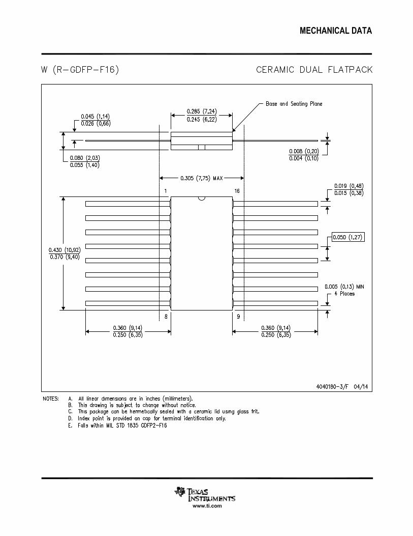
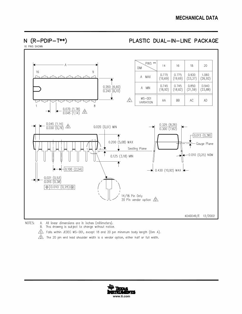
13 Mechanical, Packaging, and Orderable InformationThe following pages include mechanical, packaging, and orderable information. This information is the most current data available for the designated devices. This data is subject to change without notice and revision of this document. For browser-based versions of this data sheet, refer to the left-hand navigation.
www.ti.comSN54HC138, SN74HC138
SCLS107G – DECEMBER 1982 – REVISED OCTOBER 2021
Copyright © 2021 Texas Instruments Incorporated Submit Document Feedback 13
Product Folder Links: SN54HC138 SN74HC138

PACKAGE OPTION ADDENDUM
www.ti.com 5-Nov-2021
Addendum-Page 1
PACKAGING INFORMATION
Orderable Device Status(1)
Package Type PackageDrawing
Pins PackageQty
Eco Plan(2)
Lead finish/Ball material
(6)
MSL Peak Temp(3)
Op Temp (°C) Device Marking(4/5)
Samples
5962-8406201VEA ACTIVE CDIP J 16 1 Non-RoHS& Green
SNPB N / A for Pkg Type -55 to 125 5962-8406201VEASNV54HC138J
5962-8406201VFA ACTIVE CFP W 16 1 Non-RoHS& Green
SNPB N / A for Pkg Type -55 to 125 5962-8406201VFASNV54HC138W
84062012A ACTIVE LCCC FK 20 1 Non-RoHS& Green
SNPB N / A for Pkg Type -55 to 125 84062012ASNJ54HC138FK
8406201EA ACTIVE CDIP J 16 1 Non-RoHS& Green
SNPB N / A for Pkg Type -55 to 125 8406201EASNJ54HC138J
8406201FA ACTIVE CFP W 16 1 Non-RoHS& Green
SNPB N / A for Pkg Type -55 to 125 8406201FASNJ54HC138W
JM38510/65802B2A ACTIVE LCCC FK 20 1 Non-RoHS& Green
SNPB N / A for Pkg Type -55 to 125 JM38510/65802B2A
JM38510/65802BEA ACTIVE CDIP J 16 1 Non-RoHS& Green
SNPB N / A for Pkg Type -55 to 125 JM38510/65802BEA
M38510/65802B2A ACTIVE LCCC FK 20 1 Non-RoHS& Green
SNPB N / A for Pkg Type -55 to 125 JM38510/65802B2A
M38510/65802BEA ACTIVE CDIP J 16 1 Non-RoHS& Green
SNPB N / A for Pkg Type -55 to 125 JM38510/65802BEA
SN54HC138J ACTIVE CDIP J 16 1 Non-RoHS& Green
SNPB N / A for Pkg Type -55 to 125 SN54HC138J
SN74HC138D ACTIVE SOIC D 16 40 RoHS & Green NIPDAU Level-1-260C-UNLIM -40 to 85 HC138
SN74HC138DBR ACTIVE SSOP DB 16 2000 RoHS & Green NIPDAU Level-1-260C-UNLIM -40 to 85 HC138
SN74HC138DE4 ACTIVE SOIC D 16 40 RoHS & Green NIPDAU Level-1-260C-UNLIM -40 to 85 HC138
SN74HC138DG4 ACTIVE SOIC D 16 40 RoHS & Green NIPDAU Level-1-260C-UNLIM -40 to 85 HC138
SN74HC138DR ACTIVE SOIC D 16 2500 RoHS & Green NIPDAU | SN Level-1-260C-UNLIM -40 to 85 HC138
SN74HC138DRE4 ACTIVE SOIC D 16 2500 RoHS & Green NIPDAU Level-1-260C-UNLIM -40 to 85 HC138

PACKAGE OPTION ADDENDUM
www.ti.com 5-Nov-2021
Addendum-Page 2
Orderable Device Status(1)
Package Type PackageDrawing
Pins PackageQty
Eco Plan(2)
Lead finish/Ball material
(6)
MSL Peak Temp(3)
Op Temp (°C) Device Marking(4/5)
Samples
SN74HC138DRG4 ACTIVE SOIC D 16 2500 RoHS & Green NIPDAU Level-1-260C-UNLIM -40 to 85 HC138
SN74HC138DT ACTIVE SOIC D 16 250 RoHS & Green NIPDAU Level-1-260C-UNLIM -40 to 85 HC138
SN74HC138N ACTIVE PDIP N 16 25 RoHS & Green NIPDAU | SN N / A for Pkg Type -40 to 85 SN74HC138N
SN74HC138NE4 ACTIVE PDIP N 16 25 RoHS & Green NIPDAU N / A for Pkg Type -40 to 85 SN74HC138N
SN74HC138NSR ACTIVE SO NS 16 2000 RoHS & Green NIPDAU Level-1-260C-UNLIM -40 to 85 HC138
SN74HC138PW ACTIVE TSSOP PW 16 90 RoHS & Green NIPDAU Level-1-260C-UNLIM -40 to 85 HC138
SN74HC138PWR ACTIVE TSSOP PW 16 2000 RoHS & Green NIPDAU | SN Level-1-260C-UNLIM -40 to 85 HC138
SN74HC138PWRE4 ACTIVE TSSOP PW 16 2000 RoHS & Green NIPDAU Level-1-260C-UNLIM -40 to 85 HC138
SN74HC138PWRG4 ACTIVE TSSOP PW 16 2000 RoHS & Green NIPDAU Level-1-260C-UNLIM -40 to 85 HC138
SN74HC138PWT ACTIVE TSSOP PW 16 250 RoHS & Green NIPDAU Level-1-260C-UNLIM -40 to 85 HC138
SNJ54HC138FK ACTIVE LCCC FK 20 1 Non-RoHS& Green
SNPB N / A for Pkg Type -55 to 125 84062012ASNJ54HC138FK
SNJ54HC138J ACTIVE CDIP J 16 1 Non-RoHS& Green
SNPB N / A for Pkg Type -55 to 125 8406201EASNJ54HC138J
SNJ54HC138W ACTIVE CFP W 16 1 Non-RoHS& Green
SNPB N / A for Pkg Type -55 to 125 8406201FASNJ54HC138W
(1) The marketing status values are defined as follows:ACTIVE: Product device recommended for new designs.LIFEBUY: TI has announced that the device will be discontinued, and a lifetime-buy period is in effect.NRND: Not recommended for new designs. Device is in production to support existing customers, but TI does not recommend using this part in a new design.PREVIEW: Device has been announced but is not in production. Samples may or may not be available.OBSOLETE: TI has discontinued the production of the device.
(2) RoHS: TI defines "RoHS" to mean semiconductor products that are compliant with the current EU RoHS requirements for all 10 RoHS substances, including the requirement that RoHS substancedo not exceed 0.1% by weight in homogeneous materials. Where designed to be soldered at high temperatures, "RoHS" products are suitable for use in specified lead-free processes. TI mayreference these types of products as "Pb-Free".RoHS Exempt: TI defines "RoHS Exempt" to mean products that contain lead but are compliant with EU RoHS pursuant to a specific EU RoHS exemption.Green: TI defines "Green" to mean the content of Chlorine (Cl) and Bromine (Br) based flame retardants meet JS709B low halogen requirements of <=1000ppm threshold. Antimony trioxide basedflame retardants must also meet the <=1000ppm threshold requirement.

PACKAGE OPTION ADDENDUM
www.ti.com 5-Nov-2021
Addendum-Page 3
(3) MSL, Peak Temp. - The Moisture Sensitivity Level rating according to the JEDEC industry standard classifications, and peak solder temperature.
(4) There may be additional marking, which relates to the logo, the lot trace code information, or the environmental category on the device.
(5) Multiple Device Markings will be inside parentheses. Only one Device Marking contained in parentheses and separated by a "~" will appear on a device. If a line is indented then it is a continuationof the previous line and the two combined represent the entire Device Marking for that device.
(6) Lead finish/Ball material - Orderable Devices may have multiple material finish options. Finish options are separated by a vertical ruled line. Lead finish/Ball material values may wrap to twolines if the finish value exceeds the maximum column width.
Important Information and Disclaimer:The information provided on this page represents TI's knowledge and belief as of the date that it is provided. TI bases its knowledge and belief on informationprovided by third parties, and makes no representation or warranty as to the accuracy of such information. Efforts are underway to better integrate information from third parties. TI has taken andcontinues to take reasonable steps to provide representative and accurate information but may not have conducted destructive testing or chemical analysis on incoming materials and chemicals.TI and TI suppliers consider certain information to be proprietary, and thus CAS numbers and other limited information may not be available for release.
In no event shall TI's liability arising out of such information exceed the total purchase price of the TI part(s) at issue in this document sold by TI to Customer on an annual basis.
OTHER QUALIFIED VERSIONS OF SN54HC138, SN54HC138-SP, SN74HC138 :
• Catalog : SN74HC138, SN54HC138
• Automotive : SN74HC138-Q1, SN74HC138-Q1
• Military : SN54HC138
• Space : SN54HC138-SP
NOTE: Qualified Version Definitions:
• Catalog - TI's standard catalog product
• Automotive - Q100 devices qualified for high-reliability automotive applications targeting zero defects
• Military - QML certified for Military and Defense Applications
• Space - Radiation tolerant, ceramic packaging and qualified for use in Space-based application

TAPE AND REEL INFORMATION
*All dimensions are nominal
Device PackageType
PackageDrawing
Pins SPQ ReelDiameter
(mm)
ReelWidth
W1 (mm)
A0(mm)
B0(mm)
K0(mm)
P1(mm)
W(mm)
Pin1Quadrant
SN74HC138DBR SSOP DB 16 2000 330.0 16.4 8.35 6.6 2.4 12.0 16.0 Q1
SN74HC138DR SOIC D 16 2500 330.0 16.4 6.5 10.3 2.1 8.0 16.0 Q1
SN74HC138DR SOIC D 16 2500 330.0 16.8 6.5 10.3 2.1 8.0 16.0 Q1
SN74HC138DRG4 SOIC D 16 2500 330.0 16.4 6.5 10.3 2.1 8.0 16.0 Q1
SN74HC138NSR SO NS 16 2000 330.0 16.4 8.2 10.5 2.5 12.0 16.0 Q1
SN74HC138PWR TSSOP PW 16 2000 330.0 12.4 6.9 5.6 1.6 8.0 12.0 Q1
SN74HC138PWR TSSOP PW 16 2000 330.0 12.4 6.9 5.6 1.6 8.0 12.0 Q1
SN74HC138PWRG4 TSSOP PW 16 2000 330.0 12.4 6.9 5.6 1.6 8.0 12.0 Q1
SN74HC138PWT TSSOP PW 16 250 330.0 12.4 6.9 5.6 1.6 8.0 12.0 Q1
PACKAGE MATERIALS INFORMATION
www.ti.com 5-Jan-2022
Pack Materials-Page 1

*All dimensions are nominal
Device Package Type Package Drawing Pins SPQ Length (mm) Width (mm) Height (mm)
SN74HC138DBR SSOP DB 16 2000 853.0 449.0 35.0
SN74HC138DR SOIC D 16 2500 340.5 336.1 32.0
SN74HC138DR SOIC D 16 2500 364.0 364.0 27.0
SN74HC138DRG4 SOIC D 16 2500 340.5 336.1 32.0
SN74HC138NSR SO NS 16 2000 853.0 449.0 35.0
SN74HC138PWR TSSOP PW 16 2000 853.0 449.0 35.0
SN74HC138PWR TSSOP PW 16 2000 364.0 364.0 27.0
SN74HC138PWRG4 TSSOP PW 16 2000 853.0 449.0 35.0
SN74HC138PWT TSSOP PW 16 250 853.0 449.0 35.0
PACKAGE MATERIALS INFORMATION
www.ti.com 5-Jan-2022
Pack Materials-Page 2

TUBE
*All dimensions are nominal
Device Package Name Package Type Pins SPQ L (mm) W (mm) T (µm) B (mm)
84062012A FK LCCC 20 1 506.98 12.06 2030 NA
JM38510/65802B2A FK LCCC 20 1 506.98 12.06 2030 NA
M38510/65802B2A FK LCCC 20 1 506.98 12.06 2030 NA
SN74HC138D D SOIC 16 40 507 8 3940 4.32
SN74HC138DE4 D SOIC 16 40 507 8 3940 4.32
SN74HC138DG4 D SOIC 16 40 507 8 3940 4.32
SN74HC138N N PDIP 16 25 506 13.97 11230 4.32
SN74HC138N N PDIP 16 25 506 13.97 11230 4.32
SN74HC138N N PDIP 16 25 506.1 9 600 5.4
SN74HC138NE4 N PDIP 16 25 506 13.97 11230 4.32
SN74HC138NE4 N PDIP 16 25 506 13.97 11230 4.32
SN74HC138NE4 N PDIP 16 25 506.1 9 600 5.4
SN74HC138PW PW TSSOP 16 90 530 10.2 3600 3.5
SNJ54HC138FK FK LCCC 20 1 506.98 12.06 2030 NA
PACKAGE MATERIALS INFORMATION
www.ti.com 5-Jan-2022
Pack Materials-Page 3

www.ti.com
PACKAGE OUTLINE
C
8.27.4 TYP
14X 1.27
16X 0.510.35
2X8.89
0.15 TYP
0 - 10
0.30.1
2.00 MAX
(1.25)
0.25GAGE PLANE
1.050.55
A
10.410.0
NOTE 3
B 5.45.2
NOTE 4
4220735/A 12/2021
SOP - 2.00 mm max heightNS0016ASOP
NOTES: 1. All linear dimensions are in millimeters. Dimensions in parenthesis are for reference only. Dimensioning and tolerancing per ASME Y14.5M. 2. This drawing is subject to change without notice. 3. This dimension does not include mold flash, protrusions, or gate burrs. Mold flash, protrusions, or gate burrs shall not exceed 0.15 mm, per side. 4. This dimension does not include interlead flash. Interlead flash shall not exceed 0.25 mm, per side.
1 16
0.25 C A B
98
PIN 1 IDAREA
SEATING PLANE
0.1 C
SEE DETAIL A
DETAIL ATYPICAL
SCALE 1.500

www.ti.com
EXAMPLE BOARD LAYOUT
0.07 MAXALL AROUND
0.07 MINALL AROUND
14X (1.27)
(R0.05) TYP
(7)
16X (1.85)
16X (0.6)
4220735/A 12/2021
SOP - 2.00 mm max heightNS0016ASOP
NOTES: (continued) 5. Publication IPC-7351 may have alternate designs. 6. Solder mask tolerances between and around signal pads can vary based on board fabrication site.
METAL SOLDER MASKOPENING
NON SOLDER MASKDEFINED
SOLDER MASK DETAILS
OPENINGSOLDER MASK METAL
SOLDER MASKDEFINED
LAND PATTERN EXAMPLESCALE:7X
SYMM
1
8 9
16
SEEDETAILS
SYMM

www.ti.com
EXAMPLE STENCIL DESIGN
(7)(R0.05) TYP
16X (1.85)
16X (0.6)
14X (1.27)
4220735/A 12/2021
SOP - 2.00 mm max heightNS0016ASOP
NOTES: (continued) 7. Laser cutting apertures with trapezoidal walls and rounded corners may offer better paste release. IPC-7525 may have alternate design recommendations. 8. Board assembly site may have different recommendations for stencil design.
SOLDER PASTE EXAMPLEBASED ON 0.125 mm THICK STENCIL
SCALE:7X
SYMM
SYMM
1
8 9
16


www.ti.com
PACKAGE OUTLINE
C
14X 0.65
2X4.55
16X 0.300.19
TYP6.66.2
1.2 MAX
0.150.05
0.25GAGE PLANE
-80
BNOTE 4
4.54.3
A
NOTE 3
5.14.9
0.750.50
(0.15) TYP
TSSOP - 1.2 mm max heightPW0016ASMALL OUTLINE PACKAGE
4220204/A 02/2017
1
89
16
0.1 C A B
PIN 1 INDEX AREA
SEE DETAIL A
0.1 C
NOTES: 1. All linear dimensions are in millimeters. Any dimensions in parenthesis are for reference only. Dimensioning and tolerancing per ASME Y14.5M. 2. This drawing is subject to change without notice. 3. This dimension does not include mold flash, protrusions, or gate burrs. Mold flash, protrusions, or gate burrs shall not exceed 0.15 mm per side. 4. This dimension does not include interlead flash. Interlead flash shall not exceed 0.25 mm per side.5. Reference JEDEC registration MO-153.
SEATINGPLANE
A 20DETAIL ATYPICAL
SCALE 2.500

www.ti.com
EXAMPLE BOARD LAYOUT
0.05 MAXALL AROUND
0.05 MINALL AROUND
16X (1.5)
16X (0.45)
14X (0.65)
(5.8)
(R0.05) TYP
TSSOP - 1.2 mm max heightPW0016ASMALL OUTLINE PACKAGE
4220204/A 02/2017
NOTES: (continued) 6. Publication IPC-7351 may have alternate designs. 7. Solder mask tolerances between and around signal pads can vary based on board fabrication site.
LAND PATTERN EXAMPLEEXPOSED METAL SHOWN
SCALE: 10X
SYMM
SYMM
1
8 9
16
15.000
METALSOLDER MASKOPENING
METAL UNDERSOLDER MASK
SOLDER MASKOPENING
EXPOSED METALEXPOSED METAL
SOLDER MASK DETAILS
NON-SOLDER MASKDEFINED
(PREFERRED)
SOLDER MASKDEFINED

www.ti.com
EXAMPLE STENCIL DESIGN
16X (1.5)
16X (0.45)
14X (0.65)
(5.8)
(R0.05) TYP
TSSOP - 1.2 mm max heightPW0016ASMALL OUTLINE PACKAGE
4220204/A 02/2017
NOTES: (continued) 8. Laser cutting apertures with trapezoidal walls and rounded corners may offer better paste release. IPC-7525 may have alternate design recommendations. 9. Board assembly site may have different recommendations for stencil design.
SOLDER PASTE EXAMPLEBASED ON 0.125 mm THICK STENCIL
SCALE: 10X
SYMM
SYMM
1
8 9
16


MECHANICAL DATA
MSSO002E – JANUARY 1995 – REVISED DECEMBER 2001
POST OFFICE BOX 655303 • DALLAS, TEXAS 75265
DB (R-PDSO-G**) PLASTIC SMALL-OUTLINE
4040065 /E 12/01
28 PINS SHOWN
Gage Plane
8,207,40
0,550,95
0,25
38
12,90
12,30
28
10,50
24
8,50
Seating Plane
9,907,90
30
10,50
9,90
0,38
5,605,00
15
0,22
14
A
28
1
2016
6,506,50
14
0,05 MIN
5,905,90
DIM
A MAX
A MIN
PINS **
2,00 MAX
6,90
7,50
0,65 M0,15
0°–8°
0,10
0,090,25
NOTES: A. All linear dimensions are in millimeters.B. This drawing is subject to change without notice.C. Body dimensions do not include mold flash or protrusion not to exceed 0,15.D. Falls within JEDEC MO-150

IMPORTANT NOTICE AND DISCLAIMERTI PROVIDES TECHNICAL AND RELIABILITY DATA (INCLUDING DATA SHEETS), DESIGN RESOURCES (INCLUDING REFERENCE DESIGNS), APPLICATION OR OTHER DESIGN ADVICE, WEB TOOLS, SAFETY INFORMATION, AND OTHER RESOURCES “AS IS” AND WITH ALL FAULTS, AND DISCLAIMS ALL WARRANTIES, EXPRESS AND IMPLIED, INCLUDING WITHOUT LIMITATION ANY IMPLIED WARRANTIES OF MERCHANTABILITY, FITNESS FOR A PARTICULAR PURPOSE OR NON-INFRINGEMENT OF THIRD PARTY INTELLECTUAL PROPERTY RIGHTS.These resources are intended for skilled developers designing with TI products. You are solely responsible for (1) selecting the appropriate TI products for your application, (2) designing, validating and testing your application, and (3) ensuring your application meets applicable standards, and any other safety, security, regulatory or other requirements.These resources are subject to change without notice. TI grants you permission to use these resources only for development of an application that uses the TI products described in the resource. Other reproduction and display of these resources is prohibited. No license is granted to any other TI intellectual property right or to any third party intellectual property right. TI disclaims responsibility for, and you will fully indemnify TI and its representatives against, any claims, damages, costs, losses, and liabilities arising out of your use of these resources.TI’s products are provided subject to TI’s Terms of Sale or other applicable terms available either on ti.com or provided in conjunction with such TI products. TI’s provision of these resources does not expand or otherwise alter TI’s applicable warranties or warranty disclaimers for TI products.TI objects to and rejects any additional or different terms you may have proposed. IMPORTANT NOTICE
Mailing Address: Texas Instruments, Post Office Box 655303, Dallas, Texas 75265Copyright © 2022, Texas Instruments Incorporated