sinusoidal oscillators /1
TRANSCRIPT

04/03/2019
1
1
Sinusoidal Oscillators /1
• A sinusoidal oscillator is a system described by two conjugate
imaginary poles
• A linear amplifier can be closed within a feedback loop in order to
build an oscillator, if Barkhausen condition is satisfied, i.e. the
system shows a pair of conjugate imaginary poles
0)()(1 jAjf
RL
)j(A
)j(f
2
Sinusoidal Oscillators /2• Barkhausen condition means that system oscillation is self-sustained, i.e.
the loop gain is equal to 1 (Zi is the input impedance of block A):
• The complex condition corresponds to 2 real conditions:
or
RL
)j(A
)j(f
Zi
Zi
Vi
ii VjAjfV )()(
0)]()(Im[
1)]()(Re[
jAjf
jAjf
2)]()([
1)()(
kjAjfArg
jAjf

04/03/2019
2
3
Resonant networks - 1
• The transfer function of a resonant network contains a pair of
conjugate complex poles (at least a L-C pair is needed)
• The resonance frequency is defined as the frequency where
the transfer function is real (and also maximum)
• Please, let’s consider a series resonant network as the
following one.
I
4
Resonant networks - 2
If we evaluate the current flowing in the loop: I(j)= V (j)Y(j)
) ) ) CLs1sCR
sC
sLsC
1R
1
sV
sIsY
2
The network poles of the transfer function Y(s) are:
)LC
LCRCRCS
2
42
2,1

04/03/2019
3
5
Resonant networks - 3
)
jCR
L
L
R
LCL
R
L
R
LC
LCRCRCS
2
22
2,1
411
2
1
222
4
The cutoff radian frequency 0 is evaluated as the modulus of
the conjugate complex poles:
LC
1220
6
Resonant networks - 4
C
L
R
1
LC
RL
R
L
RI2/1
LI2/1
P
EQ 0
2
20
diss
imm0
The quality factor Q of the resonant network is defined as the ratio:
where Eimm is the average energy stored in the network at radian
frequency 0, and Pdiss is the average dissipated power in network
resistors (i.e. the average power loss)
Poles can be expressed as a function of Q and 0:
LC
1220
20
2
02,14
11
241
2 Qj
L
R
L
CRj
L
RS

04/03/2019
4
7
Resonant networks - 5
Phase (degrees) and Modulus (dB) of the transfer function by
considering R (losses) as a parameter: a steeper phase and a
higher modulus is found around 0
R: 101
8
Resonant networks - 6
R: 10.1

04/03/2019
5
9
Resonant networks - 7
The -3dB bandwidth of the resonant network transfer function
can be related in a simple way to the quality factor Q
For instance, if we consider the series resonant network
previously presented, we have at resonant frequency:
that is just the maximum value for the transfer function
Let’s evaluate the frequency at which 3dB power attenuation
is obtained
)R
1Y 0
10
Resonant networks - 8
The modulus of the transfer function can be expressed as:
)
)
2
2
2o222
2
2222
22
1LR
1
LC
11LR
1
C
1LR
1jY
LjCj
1R
1jY

04/03/2019
6
11
Resonant networks - 9
L22
L
LLR
0
0
odB3
dB3
odB3
dB3
2o
2dB3
The fractional bandwidth (FBW) is defined as the ratio of the
bilateral -3dB bandwidth (BW = 2) on the resonance radian
frequency. We find:
Q
1
L2
R2BWFBW
00
12
Resonant networks - 10
As the Q factor increases, a steeper phase transition as well as a
lower -3dB bandwidth (i.e. more frequency selectivity) are
obtained
Both the above mentioned property can be exploited in order to
design a frequency-stable oscillator:
1) Frequency selectivity allows decreasing of the effect of
amplifier additive noise: lower phase noise is obtained, we’ll see
later…
2) Steep phase transition of the resonant network makes the
oscillation frequency less dependent on amplifier characteristics
variation

04/03/2019
7
13
Resonant networks - 11
)
0d
dS 0F
The frequency stability coefficient SF gives us an idea of the
variation speed of the phase of the transfer function around
the resonance frequency:
An approximate estimation can be obtained for a resonant
network showing quality factor Q:
Q2SF
14
Resonant networks - 12
From expressions above, we can see that resistive loss has
to be reduced in order to increase the Q factor
Resistive loss is due to:
1) Loss in passive components.
2) Real parts of active device (BJT or MOS) impedances

04/03/2019
8
15
Passive component models - 1
Capacitor, inductors, and transformers are affected by both
loss and self-resonance:
• Loss is accounted for in the model by means of a resistor
• In order to account for self-resonance, a dual component has
to be inserted in the model (L C)
16
Passive component models - 2
Ideal capacitor
Lossy capacitor
Lossy capacitor with self-resonance
A RF capacitor shows a set of harmonic self-resonance frequencies:
It can be used only below the lowest resonance frequency.

04/03/2019
9
17
Passive component models - 3
• Loss is caused by finite resistance of both
dielectrics and conductors
• In capacitors, the capacitance is increased by
increasing area and / or by lowering plates mutual
distance: in both cases, for a given dielectric
material, resistance is lowered
• Moreover, in capacitors also radiation loss has to
be considered, as the e.m. field is not confined
18
Passive component models - 4
• The presence of an inductor in the capacitor model
allows modeling of both magnetic loss of access
metallic pins, and cavity resonance modes
• Inductor loss is due to conductor electric loss and,
at higher frequencies, to the so-called skin effect that
produces series resistance increase
• The presence of a capacitor in the inductor model
allows modeling of mutual parasitic capacitance
between inductor coils
04/03/2019
10
19
Passive component models - 5
• As a consequence of loss effect, the quality factor of real
networks is lowered and therefore frequency selectivity (-3dB
bandwidth is increased)
• A quality factor Q is considered also for the single passive
component (L and C)
20
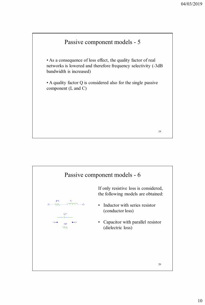
Passive component models - 6
If only resistive loss is considered,
the following models are obtained:
• Inductor with series resistor
(conductor loss)
• Capacitor with parallel resistor
(dielectric loss)

04/03/2019
11
21
Passive component models - 7
PPC
PCC
SLL
CsR1
R)s(Z
sLR)s(Z
The Q factor of a component (an inductor, for
instance) with series model can be defined as the
ratio of reactance on resistance sLsL
R
LQ
pCpC CRQ The Q factor of a component (a capacitor, for
instance) with parallel model can be defined as
the ratio of susceptance on conductance
22
Passive component models - 8
It is possible to consider a parallel
model for the inductor
and a series model for the capacitor
LjRLjR
LjRZ sL
ppL
ppLpL
At a fixed frequency we can write:

04/03/2019
12
23
Passive component models - 9
)
2
2
pL
2
p
2
pL
2
P
2
2
pL
2
pLppL
2
P
2
2
pL
2
P
2
2
pL
2
pLppL
2
P
2
2
P
22
pL
2
pLppL
2
P
2
2
ppL
ppLppL
ppL
ppL
pL
Q
11Q
R
Q
11
Lj
R
L1R
RLjRL
R
L1R
RLjRL
LR
RLjRL
LjR
LjRLjR
LjR
LjRZ
24
Passive component models - 10
2
pL
2
2
pLS
p
2
pS
2
2
pL
2
ppL
Q
R
Q
11Q
RR
L
Q
11
LL
Q
11Q
R
Q
11
LjZ
The quality factor is dependent
on frequency: it is lowered as
frequency increases: see RF
components datasheets

04/03/2019
13
25
Passive component models - 11
L - R MODEL C - R MODEL
QS = LS / RS QS = 1 / ( RS CS)
QP = RP / LP QP = RP CP
RP = RS (1 + QS2) RS = RP / (1 + QP
2)
LP = LS (1 + 1 / QS2) CS = CP (1 + 1 / QP
2)
TRANSFORMATIONS TABEL
26
Colpitts network - 1
R1 and R2 contain loading of the BJT used to close the
oscillator loop (we’ll see later), and the quality factor model
of capacitors C1 and C2

04/03/2019
14
27
Colpitts network - 2
The Vout/Iin transfer function is evaluated, as the BJT can be
considered as a voltage-controlled current source
) ) ) ) 21212211In
Out
CCsGGsCGsCGsL
1s
I
V
The poles of the network and the resonance frequency are
evaluated from coefficients of transfer function denominator
) ) ) )
0GG
CCGLGsGCGCLsCLCs
CCsGGsCGsCGsLsD
12
212112212
213
21212211
28
Colpitts network - 3
The resonance frequency is evaluated by putting to 0 the imaginary
part of denominator:
The real part of complex poles is needed in order to find the Q factor.
It is evaluated by exploiting the relation between poles and
polynomial coefficients:
)
21
2121
21
21
2121
212120
2121021300
CC
CCL
1
CC
GG
CC
CCL
1
CLC
CCGLG
0CCGLGjCLCjjD
) ) ) )
2021
121
21
12*221
12
212112212
213
21212211
1
CLC
GGs
CLC
GGsss
0GG
CCGLGsGCGCLsCLCs
CCsGGsCGsCGsLsD
( 0)
04/03/2019
15
29
Colpitts network - 4
The real part of complex poles is derived by considering the sum
of poles:
21
1221*221
CC
GCGCsss
21
12
21
1221
2021
12
21
12212
CC
GG
CC
GCGC1
CLC
GG
CC
GCGCsRe2
) ) )
) )2121
12
222
1
2121
122121211212
CCCC
GCGC
CCCC
GCGCCCCCGCCG
121
12212 s
CC
GCGCsRe2
)
)12
222
1
21210
2
0
GCGC
CCCC
sRe2Q
30
Under the hypothesis:
Qc1 >> Qc2 => Q Qc2
VOut(0) = - Iin(0) / [(C1+C2)(G2/C2 + G1/C1) – (G1 + G2)]
=- Iin(0) / [(C1/C2) G2 + [(C2/C1) G1]
C1 >> C2 => VOut(0) = - Iin(0) / [(C1/C2) G2]
)
) )
) )
)2c21c1
212c1c
12
222
1
21210
210
210
12
222
1
21210
2
0
QCQC
CCQQ
GCGC
CCCC
)GG/(
)GG/(
GCGC
CCCC
sRe2Q
Colpitts network - 5

04/03/2019
16
31
Colpitts network - 6
Yin = [s3 LC1C2 + s2 LG C2 + s (C1+C2) + G] / [s2 L C1 + s L G + 1]
Zin = R [(1 - 02L C1) + j 0 G L] / [1 - 0
2L C2] per 0
Rin = R [1 - 02L C1] / [1 - 0
2L C2] = R (C1/C2)2
Xin = 0 L / [1 - 02L C2] = - (Qc2/Qc1) 0 L
Input impedance
evaluation:
32
Sinusoidal Oscillators /3
• Barkhausen condition is never perfectly fulfilled: indeed, poles can
shift both horizontally (oscillation vanishing or saturating), and
vertically (oscillation frequency variation)
• Stability coefficient SF allows evaluation of oscillation frequency
sensitivity to both noise and interference
• If we suppose that Barkhausen condition is satisfied for a frequency
f0’ different from f0, we can consider a first-order Taylor series
expansion of the phase if transfer function:
• Lower frequency shift is obtained for higher SF value
FS
d
d
1'
)'()(0)'(
00
0000
0

04/03/2019
17
33
Sinusoidal Oscillators /4
COLPITTS OSCILLATOR (RLC)
34
Sinusoidal Oscillators /5
COLPITTS OSCILLATOR (RLC)
• The Colpitts oscillator is composed of an amplifier stage (common
emitter) and a Colpitts network
• The amplifier produces 180° phase shift at all frequencies (under the
hypothesis that the high cut-off frequency is much greater than f0), the
Colpitts network only at the resonance frequency: the Barkhausen
condition is fulfilled at the resonance frequency provided that the loop
gain is just equal to 1 at f0
• The presence of a Radio Frequency Coil (RFC) allows to double the
maximum output dynamic

04/03/2019
18
35
Sinusoidal Oscillators /6
COLPITTS OSCILLATOR (RLC)
• Oscillation condition on loop gain modulus is applied by exploiting
Colpitts network properties. Non-idealities of the amplifier block are
moved into the Colpitts network:
• where R1’= RL // ro // R1 RL, R2’= R3 // R4 // r // R2 (R1 and R2 are used
to model capacitors loss, i.e. Ri = Qci / 0 Ci, i=1, 2)
+
-
G
C1C2 R1'R2'
Iout
36
Sinusoidal Oscillators /7
COLPITTS OSCILLATOR (RLC)
• Under the hypothesis that Qc1 >> Qc2, the overall loop gain is equal to:
– Vbe = - Iout RL C2/C1
• On the other hand, the output current of the amplifier block is:
– Iout = -gm Vbe
• Barkhausen condition is fulfilled if:
– gm = IQ / VT = C1/ (RL C2)
• In order to increase frequency stability of the oscillator, a quartz is used as
a reactive element in the Colpitts network
04/03/2019
19
37
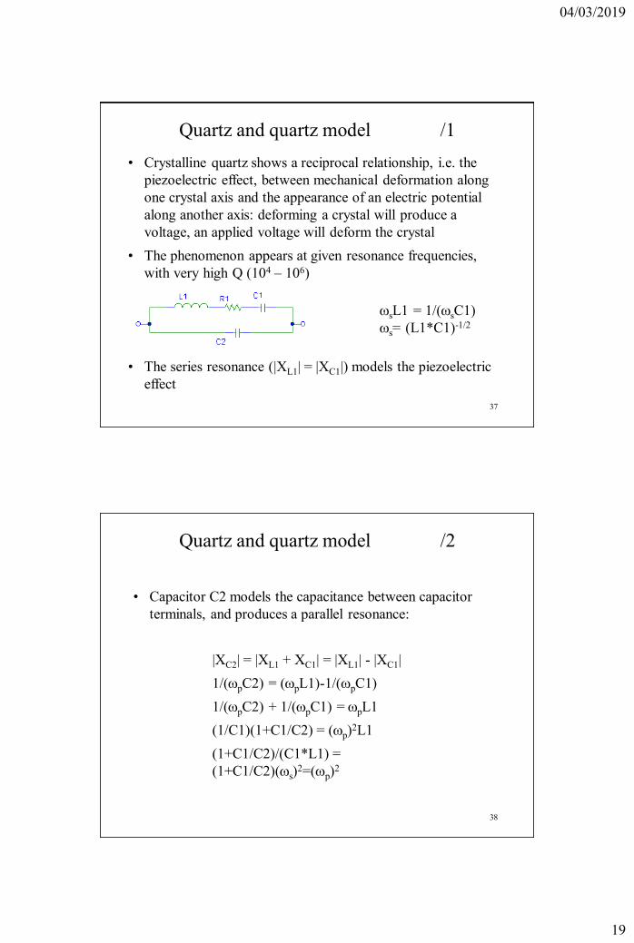
Quartz and quartz model /1
sL1 = 1/(sC1)
s= (L1*C1)-1/2
• Crystalline quartz shows a reciprocal relationship, i.e. the
piezoelectric effect, between mechanical deformation along
one crystal axis and the appearance of an electric potential
along another axis: deforming a crystal will produce a
voltage, an applied voltage will deform the crystal
• The phenomenon appears at given resonance frequencies,
with very high Q (104 – 106)
• The series resonance (|XL1| = |XC1|) models the piezoelectric
effect
38
Quartz and quartz model /2
• Capacitor C2 models the capacitance between capacitor
terminals, and produces a parallel resonance:
|XC2| = |XL1 + XC1| = |XL1| - |XC1|
1/(pC2) = (pL1)-1/(pC1)
1/(pC2) + 1/(pC1) = pL1
(1/C1)(1+C1/C2) = (p)2L1
(1+C1/C2)/(C1*L1) =
(1+C1/C2)(s)2=(p)
2

04/03/2019
20
39
Quartz and quartz model /3
p= s (1+C1/C2)1/2
If C1<<C2, a Taylor-series expansion can be considered:
(1+C1/C2)1/2= 1+(1/2)(C1/C2)
Difference between resonance frequencies p and s is:
= p - s
= (1/2)(C1/C2) s
From quartz reactance diagram above shown, it can be seen
that an inductive impedance is found between s and p
40
Sinusoidal Oscillators /7
WIEN OSCILLATOR (RC)

04/03/2019
21
41
Sinusoidal Oscillators /8
WIEN OSCILLATOR (RC)
• The amplifier block A is a non-inverting feedback amplifier showing
gain: A(j) = 1 + R2 / R1.
• If an ideal operational amplifier is considered, the input impedance is
much greater than the one of the resonant network, and the output
impedance is much lower than the load
• The loss of the resonant is evaluated, and than Barkhausen condition is
applied:
1R
RR
1CRj3CR
CRj)j(A)j(f
1
21
222
42
Sinusoidal Oscillators /9
WIEN OSCILLATOR (RC)
• The network resonance frequency is found when denominator is purely
imaginary, and therefore we get the following expression:
• From Barkhausen condition on module, the gain of operational
amplifier has to be equal to 3
• A low value of SF (=2/3) is found
CR
10
04/03/2019
22
43
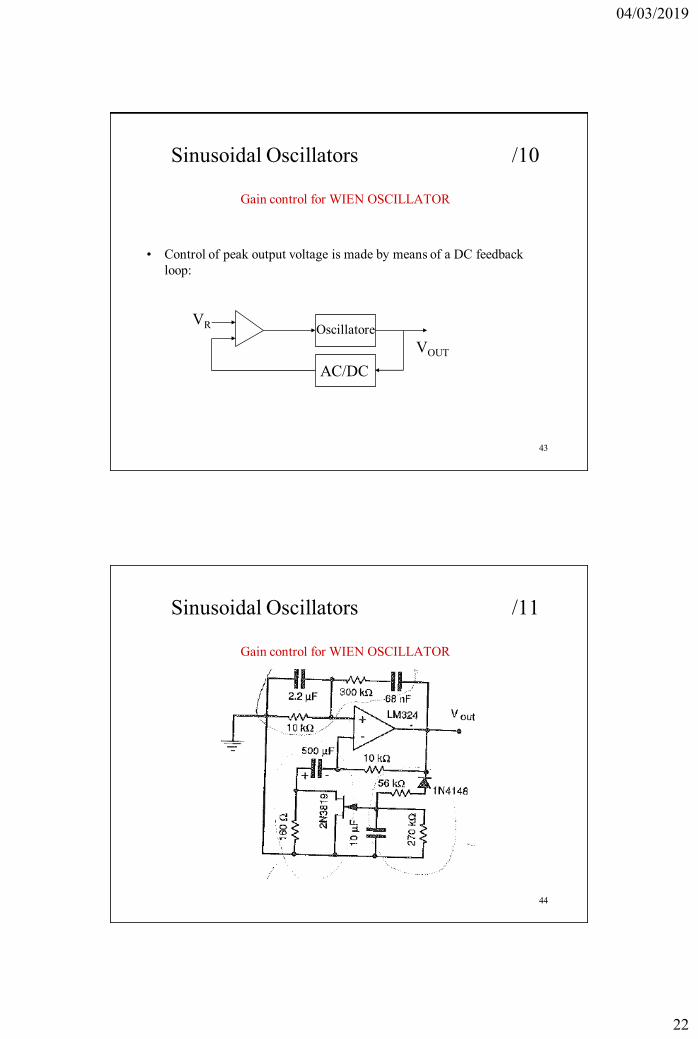
Sinusoidal Oscillators /10
Gain control for WIEN OSCILLATOR
• Control of peak output voltage is made by means of a DC feedback
loop:
VR
VOUT
AC/DC
Oscillatore
44
Sinusoidal Oscillators /11
Gain control for WIEN OSCILLATOR

04/03/2019
23
45
Sinusoidal Oscillators /12
Gain control for WIEN OSCILLATOR
• Diode and low-pass filter allow reading of the negative peak of the
waveform, so to change the bias point (VGS) of the JFET
• The JFET is biased at IDS = 0 (see the 500uF capacitor), and therefore
its resistance is changed by controlling VGS
• For instance, if waveform peak is rising, VGS is lowered, and JFET
resistance becomes greater so that the overall value of R1 is increased,
so lowering the gain of operational amplifier
46
Pierce Oscillator
quarzo

04/03/2019
24
47
DC Analysis
• The amplifier is in CE connection
• The needed output dynamic is 12 Vpp
• The oscillation frequency is 12 MHz
• The power supply is Vcc = 12V, the load R0 = 50
48
Bias point choice
• Component NPN BFG92A/X is used
• IQ = 3 mA is the bias current
• R3 = 0.67 K, R1 = 9.2 K, R2 = 2.8 K

04/03/2019
25
49
Small-signal model (Colpitts network)
Qy LjZ
)Cj/1(||R)Cj/1(||r||R||RZ 1Tot121B
)Cj/1(||RZ eq0inC
50
Oscillation conditions /1
beYBC
BCbem V
ZZZ
ZZVg
Ceq1C
eq1
eq1Q
Tot0ineq1
eq1
eq1Q
20
11
)CC
CC(L
1
RRCC
1
)CC
CC(L
1

04/03/2019
26
51
Oscillation conditions /2
1)C/GC/G)(CC()GG(
g
1Toteq0ineq1Tot0in
m
1C/C
Rg
eq1
0inm
52
Matching network use

04/03/2019
27
53
Tapped resonant circuits /1
b) Tapped-capacitor circuita) Tapped-inductor circuit
C1
L1RSRL
C2
L2
RL
C L
RS
54
Tapped resonant circuits /2
• A first Parallel->Series transformation (resistance is
lowered):
22C
L2
2C
LLS
222C
22C
2S2
Q
R
Q1
1RR
CQ
Q1CC
C1
RLS
C2SL

04/03/2019
28
55
Tapped resonant circuits /3
• A second Series -> Parallel transformation
(resistance is enhanced):
RTOTCL )
) ) ) 2
2C
2C
L22C
2C
L2CLSTOT
S21
S21
2C
2C
S21
S21
Q
QR
Q1
Q1RQ1RR
CC
CC
Q1
Q
CC
CCC
56
Tapped resonant circuits /4
• The 2nd transformation produces a parallel resonant circuit, where
input resistance is just the matching resistance at resonance
• I we consider Q expressions we find;
• The matching network produces multiplication of load resistance for a
factor depending on the ratio of capacitances
2
1
2L
2
1
21LTOT
C
C1R
C
CCRR

04/03/2019
29
57
Tapped resonant circuits /5
• Qtot = 2Q = 2f0 / BW is chosen (in order to account for partition due to
matched load).
• C value is calculated:
• L value is calculated :
• QC2 value is calculated :
Design procedure
S0
tot
R
QC
C
1L
20
1R/R
Q1Q
LS
2tot
2C
58
Tapped resonant circuits /6
• C2 value is calculated :
• C2S value is calculated :
• C1 value is calculated :
Design procedure
CC
CCC
S2
S21
L0
2C2
R
QC
22C
22C
2S2Q
Q1CC

04/03/2019
30
59
Tapped resonant circuits /7
• We need to match a 50 load to a 4K source resistance at 3.0 MHz
resonance frequency, with a loaded Q = 7.5.
• Unloaded Q value is: Qtot = 2·7.5 = 15.
• Overall capacitance is: C = 15 / (0RS) = 200 pF.
• Tuning inductance is: L = 1 / (02 C) = 14 uH.
• If the other expressions previously presented are applied, we find:
– QC2 = 1.34
– C2 = 1.4 nF
– C2S = 2.2 nF
– C1 = 0.22 nF
Design example
60
Tapped resonant circuits /8
Design example
1.0 1.5 2.0 2.5 3.0 3.5 4.0 4.5 5.0
freq, MHz
-10
-8
-6
-4
-2
0
dB
(S(1
,1))

04/03/2019
31
61
Matching network design /1
• The resonance frequency of the network is
chosen slightly lower (9/10) than the one of the
oscillator, so that the network is a capacitor at
the oscillation frequency (Ceq)
• Rin0 is given by the chosen output dinamic and
is equal to 2 K
62
• If we arbitrarily choose for the network Q = 50, we get:
• We choose:
• From network resonance frequency expression:
Matching network design /2
9.7R
RQQ
0in
0C2C nF2.5CC S22
H1L1
pF217)10/9(L
1C
201

04/03/2019
32
63
• At oscillator resonance frequency, the network
admittance is:
pF41C100/19Ceq
Matching network design /3
pF227CCC
CCC 3
S23
S23
C100/19jGC'
CjGL
1CjGY 00in2
0
20
00in
12
0
00in
64
• From condition on loop gain, we get:
• And the hypothesis: C1 >> Ceq is verified
• Oscillator resonance frequency is fixed by the
quartz, that shows inductive impedance at 0
Matching network design /4
nF46.9RgCC 0inmeq1

04/03/2019
33
65
Tapped resonant circuits /9
If we consider the tapped-inductor network, and let’s do a first
Parallel->Series transformation (load resistance RL is lowered)
Again, the transformed component values are found starting
from Q and L2
66
Tapped resonant circuits /10
22L
L2
2L
LLS
222L
22L
2S2
Q
R
Q1
1RR
LQ1
QLL
From first transformation:
The 2nd transformation (S P ) produces a parallel
resonant circuit, where input resistance is just the
matching resistance at resonance

04/03/2019
34
67
Tapped resonant circuits /11
The 2nd transformation (S P ) produces a parallel
resonant circuit, where input resistance is just the
matching resistance at resonance
68
Tapped resonant circuits /12
) )
) ) ) 2
2L
2L
L22L
2L
L2LLSTOT
S212L
2L
S21TOT
Q
QR
Q1
Q1RQ1RR
LLQ
Q1LLL
:
In S P (and P S also) transformations, Q is of course unchanged:
We can exploit such property to evaluate the parallel equivalent
resistance RTOT:

04/03/2019
35
69
Tapped resonant circuits /13
2
2
1L
2
2
21LTOT
L
L1R
L
LLRR
:
If we use Q expressions:
The matching network produces multiplication of load resistance
for a factor depending on the ratio of inductances
.
70
LC Oscillators /1
• The LC oscillator is made of a differential pair (with resistive degeneration if
needed) closed in positive feedback loop, with a tuned load L-C. The
capacitor C is often electronically changed (it is a varactor): the oscillator
shows a resonant radian frequency equal to 1/(L∙C)

04/03/2019
36
71
LC Oscillators /2
• The output resistance of the differential pair in positive feedback loop is
quite equal -1/gm of the transistor, as it can be seen from the equivalent
BARTLETT circuit for the differential pair for differential mode:
) mm
2 g/1/11g
1I/VRout
Rpigm Vpi
V2 = -V1
V2V1
II1 I2
I2 = I1
+
V
-
r gmV
72
LC Oscillators /3
• The equivalent negative resistance allows compensation of
tuned load loss: in integrated process (for instance SiGe),
inductors show low Q values (<20)
• Such loss compensation, allows to fulfill Barkhausen
condition on gain module