current-mode resistorless sinusoidal oscillators and a...
TRANSCRIPT
Indian Journal of Engineering & Materials Sciences
Vol. 23, February 2016, pp. 7-19
Current-mode resistorless sinusoidal oscillators and a dual-phase square-wave
generator using current-controlled current-differencing transconductance
amplifiers and grounded capacitors
Hung-Chun Chien*
Department of Electronic Engineering, Jinwen University of Science and Technology,
No 99, Anzhong Rd, Xindian Dist, New Taipei City, 23154, Taiwan
Received 3 February 2015; accepted 28 December 2015
In this paper, two new designs for current-mode (CM) resistorless sinusoidal oscillators based on current-controlled
current-differencing transconductance amplifiers (CCCDTAs) are presented. Each of the proposed oscillators employs a
single CCCDTA along with two grounded capacitors, and the oscillation condition and frequency can be orthogonally
controlled using the bias currents of the CCCDTA. This paper also presents a CCCDTA-based CM resistorless dual-phase
square-wave generator derived from the proposed oscillator. This paper first presents a literature review of previous designs
and then describes the applied CCCDTA as well as the relevant formulations of the proposed circuits followed by non-ideal
problems, sensitivity analyses, and computer simulation examples and results. Simulation tests of the proposed circuits
were conducted using the HSPICE program. Simulation results confirmed the theoretical analyses and validated the
proposed circuits.
Keywords: Current-controlled current-differencing transconductance amplifier (CCCDTA), Current-mode (CM) circuit,
Resistorless circuit, Sinusoidal oscillator, Square-wave generator
In electronic and electrical engineering, sinusoidal
oscillators are crucial circuits and have numerous
applications in communication modules,
instrumentation equipment, measurement interfaces,
power conversion feedback control circuits, and
portable medical devices. In early active-RC
sinusoidal oscillator designs, the operational amplifier
(OA)-based sinusoidal oscillator was the dominant
topology and these well-known topologies were
applied widely in numerous electronic circuit
systems1. However, OA-based sinusoidal oscillators
still do not satisfy the strict demands for current
sinusoidal oscillator designs because they exhibit
complex circuitry, cannot be operated at high
frequencies, and lack electronic tuning properties
required for circuit outputs. To realise optimal current
sinusoidal oscillators, four main design criteria must
be met: (1) orthogonal control of the oscillation
condition and frequency; (2) an electronic tuning law
for controlling the oscillation condition and
frequency; (3) a resistorless circuit configuration
containing grounded capacitors; and (4) no extra
buffer circuits for cascading applications. In early
designs, operational transconductance amplifier
(OTA)-based sinusoidal oscillators were widely
considered to have achieved the demand for the
electronic tuning of the oscillation condition and
frequency2.
In 2003, an active device called the current-
differencing transconductance amplifier (CDTA) was
introduced3, and a modified version called the current-
controlled current-differencing transconductance
amplifier (CCCDTA) was subsequently reported4.
CDTAs and CCCDTAs are preferred to OTAs in CM
circuit designs because they are current input and
current output active devices, whereas OTAs are
voltage input and current output active devices.
Previous studies have presented various types of
CDTA- and CCCDTA-based sinusoidal oscillator,
including single-phase, quadrature, and multiphase
sinusoidal oscillators. A CDTA-based CM quadrature
sinusoidal oscillator was constructed using two
CDTA-based CM allpass filters cascaded in a closed
loop5. In 2009, another CDTA-based design was
implemented using two CTDAs, a resistor, and two
capacitors to realise a dual-mode (DM) (voltage and
current output modes) quadrature sinusoidal
oscillator6. Tangsrirat and Tanjaroen introduced a CM
——————
*E-mail: [email protected]
INDIAN J. ENG. MATER. SCI., FEBRUARY 2016
8
resistorless CDTA-based quadrature sinusoidal
oscillator constructed using three CDTAs and two
capacitors7. Three CM resistorless schemes were also
suggested, combining two CCCDTAs and two
capacitors8.
Furthermore, a study presented a DM resistorless
third-order quadrature sinusoidal oscillator that
consisted of three CCCDTAs along with three
capacitors9. In addition to resistorless realisations
7-9,
several CDTA- and CCCDTA-based solutions for
reducing the number of active devices used have been
presented10-13
. Studies have reported results regarding
CDTA- and CCCDTA-based multiphase sinusoidal
oscillator designs. A study proposed three CM CDTA-
based three-phase sinusoidal oscillators14
. In 2007,
three CDTAs and two capacitors were used to create a
CM four-phase sinusoidal oscillator15
. An additional
approach involved employing two CCCDTAs and two
capacitors16
. Furthermore, two studies have proposed
CDTA- and CCCDTA-based CM multiphase
sinusoidal oscillators17-18
. In addition to quadrature
and multiphase oscillators5-18
, studies have reported
several CDTA- and CCCDTA-based single-phase
sinusoidal oscillators19-21
. Amongst them, the first
single-phase sinusoidal oscillator to adopt a single
CDTA was introduced in a VM topology19
. Biolek et
al.20
reported a CM solution. Both of the presented
circuits perform favourably well and enable the
oscillation condition and frequency to be controlled
orthogonally by tuning diverse circuit parameters, but
they contain excessive floating passive components
and lack an electronic manner for tuning the
oscillation frequency19-20
. Consequently, a recent
study21
presented an improved design, which contains
a single CCCDTA and two capacitors and enables the
oscillation condition and frequency to be orthogonally
controlled using the bias currents of the CCCDTA.
However, this circuit still includes a capacitor in a
floating connection. Although several configurations
of CDTA- and CCCDTA-based single-phase
sinusoidal oscillators exist19-21
, two new
configurations for CM resistorless single-phase
sinusoidal oscillators are proposed in this paper to
augment the catalogue of CDTA- and CCCDTA-
based sinusoidal oscillators. A review of the relevant
literature indicated that no oscillator topology
presented in this paper was previously published. This
study also presents a CCCDTA-based CM resistorless
dual-phase square-wave generator derived from the
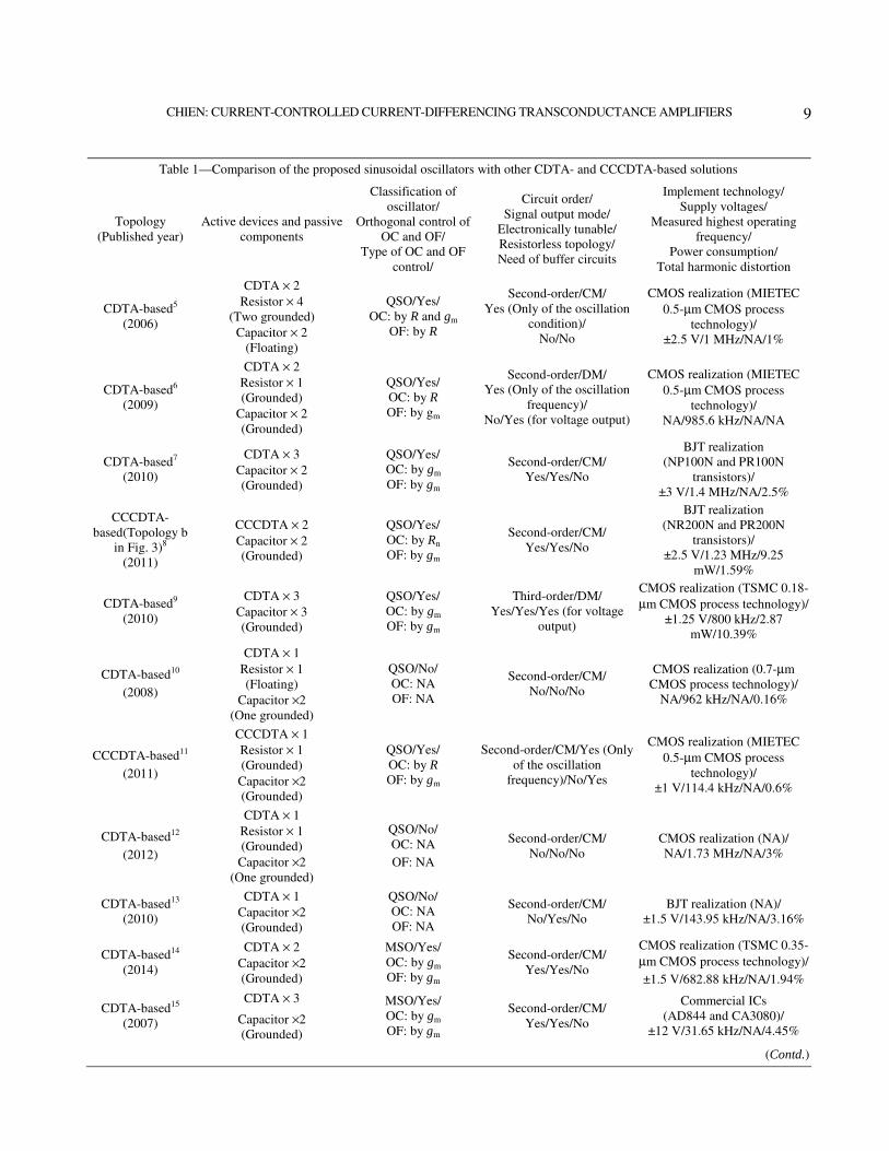
proposed oscillator as an extended design. Table 1
shows a comparison of the designs in this study and
the previous CDTA- and CCCDTA-based designs,
accentuating the novelty of the proposed sinusoidal
oscillators. Compared with previously reported
CDTA- and CCCDTA-based single-phase sinusoidal
oscillators19-21
, the proposed designs provide the
following advantages: (1) a resistorless and all-
grounded capacitor configuration, which is
advantageous from the standpoint of integrated circuit
implementation; (2) all-grounded capacitor designs
for reducing parasitic capacitance effects on the
circuit; (3) an explicit current output from a high-
output impedance terminal, which facilitates
cascading applications with other CM circuits not
requiring external buffer circuits; (4) orthogonal
control of the oscillation condition and frequency,
with electronic tuning performed by varying the bias
currents of the CCCDTA; (5) adequate active and
passive sensitivity performance levels.
Proposed Current-Mode Resistorless Sinusoidal
Oscillators and Square-wave Generator
The CCCDTA is a versatile CM active device and
its design concept originated from the CDTA.
Compared with the CDTA3, the most crucial feature
of the CCCDTA is that its intrinsic input resistances
can be adjusted by using its bias current. However,
these intrinsic resistances are equal and are controlled
by the same bias current of the CCCDTA4; thus, they
limit the flexibility of the CCCDTA in some circuit
applications. Consequently, an improved topology in
which the intrinsic resistances at the two current input
terminals (p and n terminals) can be independently
adjusted by tuning the diverse bias currents of the
CCCDTA was introduced to overcome this problem21
.
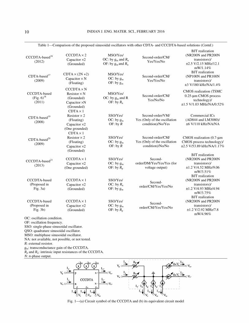
The circuit symbol and equivalent circuit model of the
CCCDTA in this study are shown in Fig. 1. The
terminals p and n represent the two current inputs
with finite intrinsic input resistances (Rp and Rn), and
the x+, x-, z, and zc terminals are the high-impedance
current outputs. The terminal characteristics of an
ideal CCCDTA are described in Eq. (1). Using this
notation, Eq. (1) shows that the currents in the z and zc
terminals are the difference between the two input
currents Ip and In and that the voltage at the z terminal
is converted to the output currents, Ix+ and Ix-, by a
transconductance gain (gm), which can be controlled
by the bias current IB2 of the CCCDTA. The intrinsic
input resistances, Rp and Rn, of the CCCDTA (Fig. 1)
are controllable by using the bias currents, IB1 and IB3,
CHIEN: CURRENT-CONTROLLED CURRENT-DIFFERENCING TRANSCONDUCTANCE AMPLIFIERS
9
Table 1—Comparison of the proposed sinusoidal oscillators with other CDTA- and CCCDTA-based solutions
Topology
(Published year)
Active devices and passive
components
Classification of
oscillator/
Orthogonal control of
OC and OF/
Type of OC and OF
control/
Circuit order/
Signal output mode/
Electronically tunable/
Resistorless topology/
Need of buffer circuits
Implement technology/
Supply voltages/
Measured highest operating
frequency/
Power consumption/
Total harmonic distortion
CDTA-based5
(2006)
CDTA × 2
Resistor × 4
(Two grounded)
Capacitor × 2
(Floating)
QSO/Yes/
OC: by R and gm
OF: by R
Second-order/CM/
Yes (Only of the oscillation
condition)/
No/No
CMOS realization (MIETEC
0.5-µm CMOS process
technology)/
±2.5 V/1 MHz/NA/1%
CDTA-based6
(2009)
CDTA × 2
Resistor × 1
(Grounded)
Capacitor × 2
(Grounded)
QSO/Yes/
OC: by R
OF: by gm
Second-order/DM/
Yes (Only of the oscillation
frequency)/
No/Yes (for voltage output)
CMOS realization (MIETEC
0.5-µm CMOS process
technology)/
NA/985.6 kHz/NA/NA
CDTA-based7
(2010)
CDTA × 3
Capacitor × 2
(Grounded)
QSO/Yes/
OC: by gm
OF: by gm
Second-order/CM/
Yes/Yes/No
BJT realization
(NP100N and PR100N
transistors)/
±3 V/1.4 MHz/NA/2.5%
CCCDTA-
based(Topology b
in Fig. 3)8
(2011)
CCCDTA × 2
Capacitor × 2
(Grounded)
QSO/Yes/
OC: by Rn
OF: by gm
Second-order/CM/
Yes/Yes/No
BJT realization
(NR200N and PR200N
transistors)/
±2.5 V/1.23 MHz/9.25
mW/1.59%
CDTA-based9
(2010)
CDTA × 3
Capacitor × 3
(Grounded)
QSO/Yes/
OC: by gm
OF: by gm
Third-order/DM/
Yes/Yes/Yes (for voltage
output)
CMOS realization (TSMC 0.18-
µm CMOS process technology)/
±1.25 V/800 kHz/2.87
mW/10.39%
CDTA-based10
(2008)
CDTA × 1
Resistor × 1
(Floating)
Capacitor ×2
(One grounded)
QSO/No/
OC: NA
OF: NA
Second-order/CM/
No/No/No
CMOS realization (0.7-µm
CMOS process technology)/
NA/962 kHz/NA/0.16%
CCCDTA-based11
(2011)
CCCDTA × 1
Resistor × 1
(Grounded)
Capacitor ×2
(Grounded)
QSO/Yes/
OC: by R
OF: by gm
Second-order/CM/Yes (Only
of the oscillation
frequency)/No/Yes
CMOS realization (MIETEC
0.5-µm CMOS process
technology)/
±1 V/114.4 kHz/NA/0.6%
CDTA-based12
(2012)
CDTA × 1
Resistor × 1
(Grounded)
Capacitor ×2
(One grounded)
QSO/No/
OC: NA
OF: NA
Second-order/CM/
No/No/No
CMOS realization (NA)/
NA/1.73 MHz/NA/3%
CDTA-based13
(2010)
CDTA × 1
Capacitor ×2
(Grounded)
QSO/No/
OC: NA
OF: NA
Second-order/CM/
No/Yes/No
BJT realization (NA)/
±1.5 V/143.95 kHz/NA/3.16%
CDTA-based14
(2014)
CDTA × 2
Capacitor ×2
(Grounded)
MSO/Yes/
OC: by gm
OF: by gm
Second-order/CM/
Yes/Yes/No
CMOS realization (TSMC 0.35-
µm CMOS process technology)/
±1.5 V/682.88 kHz/NA/1.94%
CDTA-based15
(2007)
CDTA × 3
Capacitor ×2
(Grounded)
MSO/Yes/
OC: by gm
OF: by gm
Second-order/CM/
Yes/Yes/No
Commercial ICs
(AD844 and CA3080)/
±12 V/31.65 kHz/NA/4.45%
(Contd.)
INDIAN J. ENG. MATER. SCI., FEBRUARY 2016
10
Table 1—Comparison of the proposed sinusoidal oscillators with other CDTA- and CCCDTA-based solutions (Contd.)
CCCDTA-based16
(2012)
CCCDTA × 2
Capacitor ×2
(Grounded)
MSO/Yes/
OC: by gm and Rn
OF: by gm and Rn
Second-order/CM/
Yes/Yes/No
BJT realization
(NR200N and PR200N
transistors)/
±2.5 V/2.15 MHz/12.1
mW/1.14%
CDTA-based17
(2009)
CDTA × (2N +2)
Capacitor × N
(Floating)
MSO/Yes/
OC: by gm
OF: by gm
Second-order/CM/
Yes/Yes/No
BJT realization
(NP100N and PR100N
transistors)/
±3 V/180 kHz/NA/1.4%
CCCDTA-based
(Fig. 6)18
(2011)
CCCDTA × N
Resistor × N
(Grounded)
Capacitor ×N
(Grounded)
MSO/Yes/
OC: by gm and R
OF: by Rn
Second-order/CM/
Yes/No/No
CMOS realization (TSMC
0.25-µm CMOS process
technology)/
±1.5 V/1.03 MHz/NA/0.52%
CDTA-based19
(2008)
CDTA × 1
Resistor × 2
(Floating)
Capacitor ×2
(One grounded)
SSO/Yes/
OC: by gm
OF: by R
Second-order/VM/
Yes (Only of the oscillation
condition)/No/Yes
Commercial ICs
(AD844 and LM3080)/
±6 V/110 kHz/NA/NA
CDTA-based20
(2009)
CDTA × 1
Resistor × 2
(Floating)
Capacitor ×2
(Grounded)
SSO/Yes/
OC: by gm
OF: by R
Second-order/CM/
Yes (Only of the oscillation
condition)/No/No
CMOS realization (0.7-µm
CMOS process technology)/
±2.5 V/53.89 kHz/NA/1.17%
CCCDTA-based21
(2013)
CCCDTA × 1
Capacitor ×2
(One grounded)
SSO/Yes/
OC: by gm
OF: by Rp
Second-
order/DM/Yes/Yes/Yes (for
voltage output)
BJT realization
(NR200N and PR200N
transistors)/
±1.2 V/4.52 MHz/9.06
mW/3.51%
CCCDTA-based
(Proposed in
Fig. 3a)
CCCDTA × 1
Capacitor ×2
(Grounded)
SSO/Yes/
OC: by Rn
OF: by gm
Second-
order/CM/Yes/Yes/No
BJT realization
(NR200N and PR200N
transistors)/
±1.2 V/4.93 MHz/4.94
mW/3.75%
CCCDTA-based
(Proposed in
Fig. 3b)
CCCDTA × 1
Capacitor ×2
(Grounded)
SSO/Yes/
OC: by gm
OF: by Rp
Second-
order/CM/Yes/Yes/No
BJT realization
(NR200N and PR200N
transistors)/
±1.2 V/2.92 MHz/7.8
mW/4.96%
OC: oscillation condition.
OF: oscillation frequency.
SSO: single-phase sinusoidal oscillator.
QSO: quadrature sinusoidal oscillator.
MSO: multiphase sinusoidal oscillator.
NA: not available, not possible, or not tested.
R: external resistor.
gm: transconductance gain of the CCCDTA.
Rp and Rn: intrinsic input resistances of the CCCDTA.
N: n-phase output.
Fig. 1—(a) Circuit symbol of the CCCDTA and (b) its equivalent circuit model
CHIEN: CURRENT-CONTROLLED CURRENT-DIFFERENCING TRANSCONDUCTANCE AMPLIFIERS
11
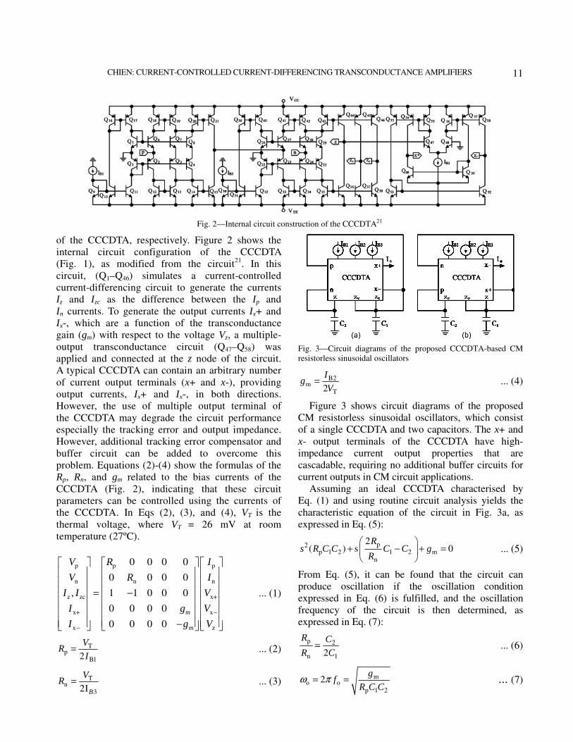
Fig. 2—Internal circuit construction of the CCCDTA21
of the CCCDTA, respectively. Figure 2 shows the
internal circuit configuration of the CCCDTA
(Fig. 1), as modified from the circuit21
. In this
circuit, (Q1–Q46) simulates a current-controlled
current-differencing circuit to generate the currents
Iz and Izc as the difference between the Ip and
In currents. To generate the output currents Ix+ and
Ix-, which are a function of the transconductance
gain (gm) with respect to the voltage Vz, a multiple-
output transconductance circuit (Q47–Q58) was
applied and connected at the z node of the circuit.
A typical CCCDTA can contain an arbitrary number
of current output terminals (x+ and x-), providing
output currents, Ix+ and Ix-, in both directions.
However, the use of multiple output terminal of
the CCCDTA may degrade the circuit performance
especially the tracking error and output impedance.
However, additional tracking error compensator and
buffer circuit can be added to overcome this
problem. Equations (2)-(4) show the formulas of the
Rp, Rn, and gm related to the bias currents of the
CCCDTA (Fig. 2), indicating that these circuit
parameters can be controlled using the currents of
the CCCDTA. In Eqs (2), (3), and (4), VT is the
thermal voltage, where VT = 26 mV at room
temperature (27ºC).
pp p
nn n
z zc x+
x+ x
x z
0 0 0 0
0 0 0 0
1 1 0 0 0,
0 0 0 0
0 0 0 0
m
m
RV I
RV I
I I V
gI V
gI V
−
−
= − −
... (1)
Tp
B12
VR
I= ... (2)
Tn
32IB
VR = ... (3)
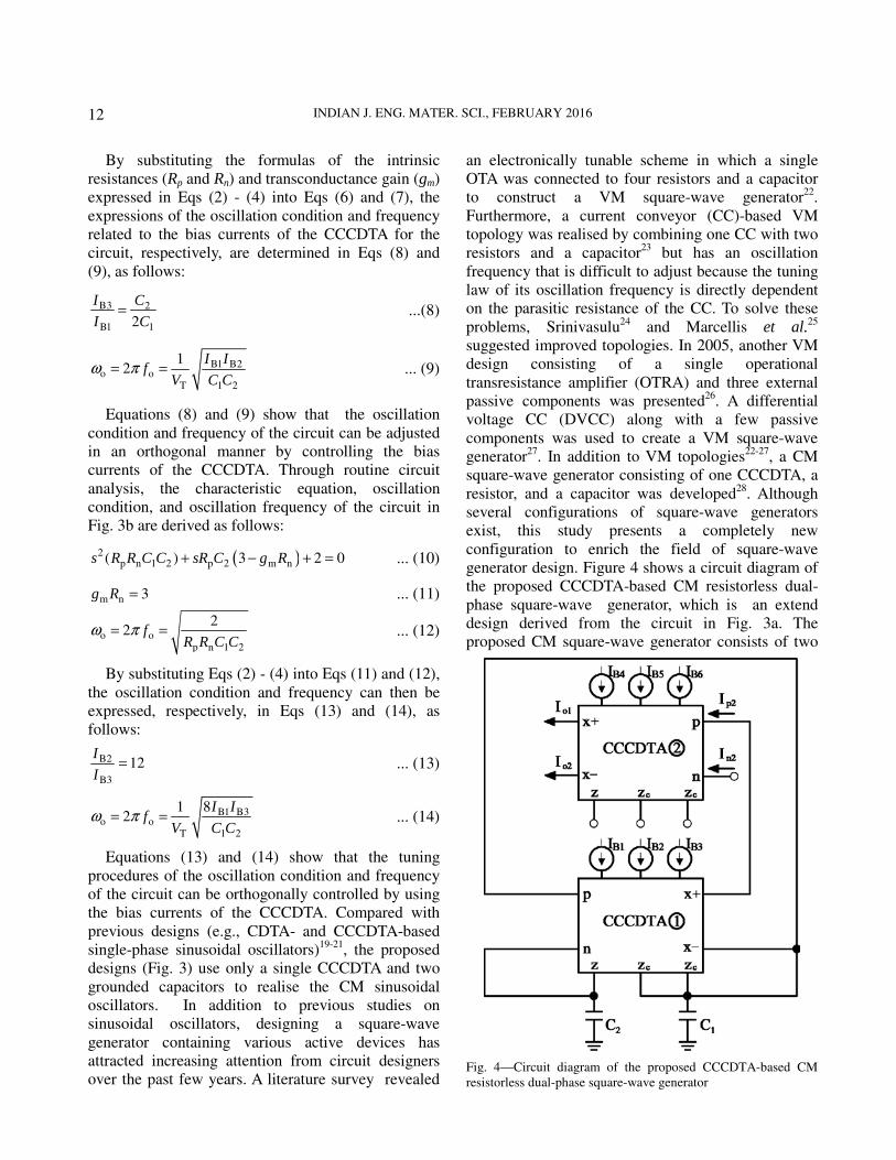
Fig. 3—Circuit diagrams of the proposed CCCDTA-based CM
resistorless sinusoidal oscillators
B2m
T2
Ig
V= ... (4)
Figure 3 shows circuit diagrams of the proposed
CM resistorless sinusoidal oscillators, which consist
of a single CCCDTA and two capacitors. The x+ and
x- output terminals of the CCCDTA have high-
impedance current output properties that are
cascadable, requiring no additional buffer circuits for
current outputs in CM circuit applications.
Assuming an ideal CCCDTA characterised by
Eq. (1) and using routine circuit analysis yields the
characteristic equation of the circuit in Fig. 3a, as
expressed in Eq. (5):
p2p 1 2 1 2 m
n
2( ) s 0
Rs R C C C C g
R
+ − + =
... (5)
From Eq. (5), it can be found that the circuit can
produce oscillation if the oscillation condition
expressed in Eq. (6) is fulfilled, and the oscillation
frequency of the circuit is then determined, as
expressed in Eq. (7):
p 2
n 12
R C
R C= ... (6)
mo o
p 1 2
2g
fR C C
ω π= = ... (7)
INDIAN J. ENG. MATER. SCI., FEBRUARY 2016
12
By substituting the formulas of the intrinsic
resistances (Rp and Rn) and transconductance gain (gm)
expressed in Eqs (2) - (4) into Eqs (6) and (7), the
expressions of the oscillation condition and frequency
related to the bias currents of the CCCDTA for the
circuit, respectively, are determined in Eqs (8) and
(9), as follows:
B3 2
B1 12
I C
I C= ...(8)
B1 B2o o
T 1 2
12
I If
V C Cω π= = ... (9)
Equations (8) and (9) show that the oscillation
condition and frequency of the circuit can be adjusted
in an orthogonal manner by controlling the bias
currents of the CCCDTA. Through routine circuit
analysis, the characteristic equation, oscillation
condition, and oscillation frequency of the circuit in
Fig. 3b are derived as follows:
( )2p n 1 2 p 2 m n( ) 3 2 0s R R C C sR C g R+ − + = ... (10)
m n 3g R = ... (11)
o op n 1 2
22 f
R R C Cω π= = ... (12)
By substituting Eqs (2) - (4) into Eqs (11) and (12),
the oscillation condition and frequency can then be
expressed, respectively, in Eqs (13) and (14), as
follows:
B2
B3
12I
I= ... (13)
B1 B3o o
T 1 2
812
I If
V C Cω π= = ... (14)
Equations (13) and (14) show that the tuning
procedures of the oscillation condition and frequency
of the circuit can be orthogonally controlled by using
the bias currents of the CCCDTA. Compared with
previous designs (e.g., CDTA- and CCCDTA-based
single-phase sinusoidal oscillators)19-21
, the proposed
designs (Fig. 3) use only a single CCCDTA and two
grounded capacitors to realise the CM sinusoidal
oscillators. In addition to previous studies on
sinusoidal oscillators, designing a square-wave
generator containing various active devices has
attracted increasing attention from circuit designers
over the past few years. A literature survey revealed
an electronically tunable scheme in which a single
OTA was connected to four resistors and a capacitor
to construct a VM square-wave generator22
.
Furthermore, a current conveyor (CC)-based VM
topology was realised by combining one CC with two
resistors and a capacitor23
but has an oscillation
frequency that is difficult to adjust because the tuning
law of its oscillation frequency is directly dependent
on the parasitic resistance of the CC. To solve these
problems, Srinivasulu24
and Marcellis et al.25
suggested improved topologies. In 2005, another VM
design consisting of a single operational
transresistance amplifier (OTRA) and three external
passive components was presented26
. A differential
voltage CC (DVCC) along with a few passive
components was used to create a VM square-wave
generator27
. In addition to VM topologies22-27
, a CM
square-wave generator consisting of one CCCDTA, a
resistor, and a capacitor was developed28
. Although
several configurations of square-wave generators
exist, this study presents a completely new
configuration to enrich the field of square-wave
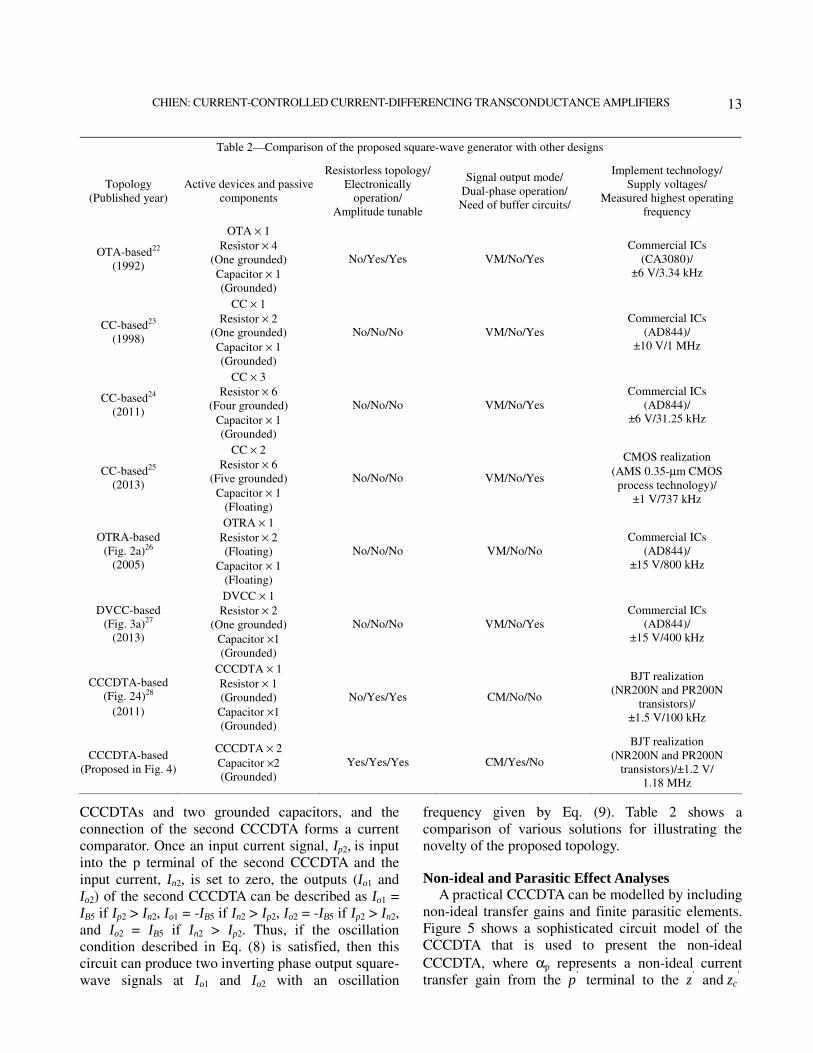
generator design. Figure 4 shows a circuit diagram of
the proposed CCCDTA-based CM resistorless dual-
phase square-wave generator, which is an extend
design derived from the circuit in Fig. 3a. The
proposed CM square-wave generator consists of two
Fig. 4—Circuit diagram of the proposed CCCDTA-based CM
resistorless dual-phase square-wave generator
CHIEN: CURRENT-CONTROLLED CURRENT-DIFFERENCING TRANSCONDUCTANCE AMPLIFIERS
13
CCCDTAs and two grounded capacitors, and the
connection of the second CCCDTA forms a current
comparator. Once an input current signal, Ip2, is input
into the p terminal of the second CCCDTA and the
input current, In2, is set to zero, the outputs (Io1 and
Io2) of the second CCCDTA can be described as Io1 =
IB5 if Ip2 > In2, Io1 = -IB5 if In2 > Ip2, Io2 = -IB5 if Ip2 > In2,
and Io2 = IB5 if In2 > Ip2. Thus, if the oscillation
condition described in Eq. (8) is satisfied, then this
circuit can produce two inverting phase output square-
wave signals at Io1 and Io2 with an oscillation
frequency given by Eq. (9). Table 2 shows a
comparison of various solutions for illustrating the
novelty of the proposed topology.
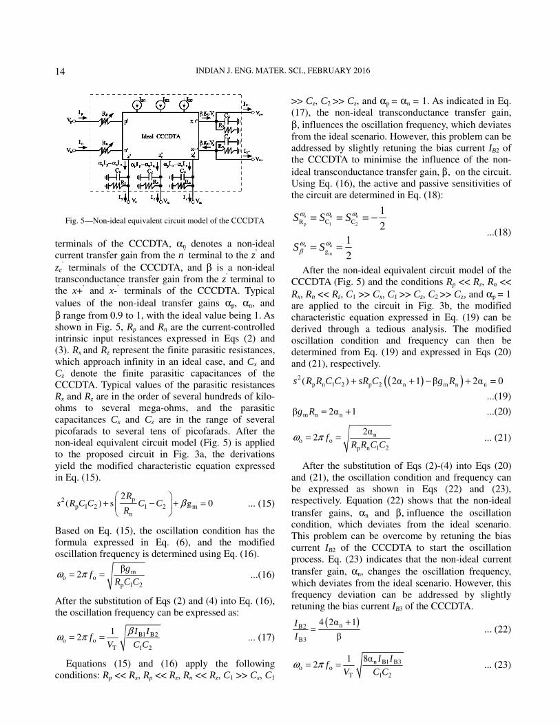
Non-ideal and Parasitic Effect Analyses A practical CCCDTA can be modelled by including
non-ideal transfer gains and finite parasitic elements.
Figure 5 shows a sophisticated circuit model of the
CCCDTA that is used to present the non-ideal
CCCDTA, where αp represents a non-ideal current
transfer gain from the p’ terminal to the z
’ and zc
’
Table 2—Comparison of the proposed square-wave generator with other designs
Topology
(Published year)
Active devices and passive
components
Resistorless topology/
Electronically
operation/
Amplitude tunable
Signal output mode/
Dual-phase operation/
Need of buffer circuits/
Implement technology/
Supply voltages/
Measured highest operating
frequency
OTA-based22
(1992)
OTA × 1
Resistor × 4
(One grounded)
Capacitor × 1
(Grounded)
No/Yes/Yes VM/No/Yes
Commercial ICs
(CA3080)/
±6 V/3.34 kHz
CC-based23
(1998)
CC × 1
Resistor × 2
(One grounded)
Capacitor × 1
(Grounded)
No/No/No VM/No/Yes
Commercial ICs
(AD844)/
±10 V/1 MHz
CC-based24
(2011)
CC × 3
Resistor × 6
(Four grounded)
Capacitor × 1
(Grounded)
No/No/No VM/No/Yes
Commercial ICs
(AD844)/
±6 V/31.25 kHz
CC-based25
(2013)
CC × 2
Resistor × 6
(Five grounded)
Capacitor × 1
(Floating)
No/No/No VM/No/Yes
CMOS realization
(AMS 0.35-µm CMOS
process technology)/
±1 V/737 kHz
OTRA-based
(Fig. 2a)26
(2005)
OTRA × 1
Resistor × 2
(Floating)
Capacitor × 1
(Floating)
No/No/No VM/No/No
Commercial ICs
(AD844)/
±15 V/800 kHz
DVCC-based
(Fig. 3a)27
(2013)
DVCC × 1
Resistor × 2
(One grounded)
Capacitor ×1
(Grounded)
No/No/No VM/No/Yes
Commercial ICs
(AD844)/
±15 V/400 kHz
CCCDTA-based
(Fig. 24)28
(2011)
CCCDTA × 1
Resistor × 1
(Grounded)
Capacitor ×1
(Grounded)
No/Yes/Yes CM/No/No
BJT realization
(NR200N and PR200N
transistors)/
±1.5 V/100 kHz
CCCDTA-based
(Proposed in Fig. 4)
CCCDTA × 2
Capacitor ×2
(Grounded)
Yes/Yes/Yes CM/Yes/No
BJT realization
(NR200N and PR200N
transistors)/±1.2 V/
1.18 MHz
INDIAN J. ENG. MATER. SCI., FEBRUARY 2016
14
Fig. 5—Non-ideal equivalent circuit model of the CCCDTA
terminals of the CCCDTA, αn denotes a non-ideal
current transfer gain from the n’ terminal to the z
’ and
zc’ terminals of the CCCDTA, and β is a non-ideal
transconductance transfer gain from the z’ terminal to
the x+’ and x-
’ terminals of the CCCDTA. Typical
values of the non-ideal transfer gains αp, αn, and
β range from 0.9 to 1, with the ideal value being 1. As
shown in Fig. 5, Rp and Rn are the current-controlled
intrinsic input resistances expressed in Eqs (2) and
(3). Rx and Rz represent the finite parasitic resistances,
which approach infinity in an ideal case, and Cx and
Cz denote the finite parasitic capacitances of the
CCCDTA. Typical values of the parasitic resistances
Rx and Rz are in the order of several hundreds of kilo-
ohms to several mega-ohms, and the parasitic
capacitances Cx and Cz are in the range of several
picofarads to several tens of picofarads. After the
non-ideal equivalent circuit model (Fig. 5) is applied
to the proposed circuit in Fig. 3a, the derivations
yield the modified characteristic equation expressed
in Eq. (15).
p2p 1 2 1 2 m
n
2( ) s g 0
Rs R C C C C
Rβ
+ − + =
... (15)
Based on Eq. (15), the oscillation condition has the
formula expressed in Eq. (6), and the modified
oscillation frequency is determined using Eq. (16).
mo o
p 1 2
β2
gf
R C Cω π= = ...(16)
After the substitution of Eqs (2) and (4) into Eq. (16),
the oscillation frequency can be expressed as:
B1 B2o o
T 1 2
12
I If
V C C
βω π= = ... (17)
Equations (15) and (16) apply the following
conditions: Rp << Rx, Rp << Rz, Rn << Rz, C1 >> Cx, C1
>> Cz, C2 >> Cz, and αp = αn = 1. As indicated in Eq.
(17), the non-ideal transconductance transfer gain,
β, influences the oscillation frequency, which deviates
from the ideal scenario. However, this problem can be
addressed by slightly retuning the bias current IB2 of
the CCCDTA to minimise the influence of the non-
ideal transconductance transfer gain, β, on the circuit.
Using Eq. (16), the active and passive sensitivities of
the circuit are determined in Eq. (18):
o o o
p 1 2
o o
m
R C C
g
1
2
1
2
S S S
S S
ω ω ω
ω ωβ
= = = −
= =
...(18)
After the non-ideal equivalent circuit model of the
CCCDTA (Fig. 5) and the conditions Rp << Rz, Rn <<
Rx, Rn << Rz, C1 >> Cx, C1 >> Cz, C2 >> Cz, and αp = 1
are applied to the circuit in Fig. 3b, the modified
characteristic equation expressed in Eq. (19) can be
derived through a tedious analysis. The modified
oscillation condition and frequency can then be
determined from Eq. (19) and expressed in Eqs (20)
and (21), respectively.
( )( )2p n 1 2 p 2 n m n n( ) 2α 1 β 2α 0s R R C C sR C g R+ + − + =
...(19)
m n nβ 2α 1g R = + ...(20)
no o
p n 1 2
2α2 f
R R C Cω π= = ... (21)
After the substitution of Eqs (2)-(4) into Eqs (20)
and (21), the oscillation condition and frequency can
be expressed as shown in Eqs (22) and (23),
respectively. Equation (22) shows that the non-ideal
transfer gains, αn and β, influence the oscillation
condition, which deviates from the ideal scenario.
This problem can be overcome by retuning the bias
current IB2 of the CCCDTA to start the oscillation
process. Eq. (23) indicates that the non-ideal current
transfer gain, αn, changes the oscillation frequency,
which deviates from the ideal scenario. However, this
frequency deviation can be addressed by slightly
retuning the bias current IB3 of the CCCDTA.
( )nB2
B3
4 2α 1
β
I
I
+= ... (22)
n B1 B3o o
T 1 2
8α12
I If
V C Cω π= = ... (23)
CHIEN: CURRENT-CONTROLLED CURRENT-DIFFERENCING TRANSCONDUCTANCE AMPLIFIERS
15
Based on Eq. (21), the active and passive sensitivities
of the circuit can be derived using Eq. (24).
o o o o
p n 1 2
o
n
R R C C
1
2
1
2
S S S S
S
ω ω ω ω
ωα
= = = = −
=
... (24)
Equations (18) and (24) indicate that the values of
all of the active and passive sensitivities are low and
do not exceed 50% in magnitude; thus, the circuits
exhibit adequate active and passive sensitivity
performance levels. Keep in mind that to minimize
the influence of the parasitic elements on the
proposed circuits, the following conditions must be
satisfied in the design procedures: Rp << Rx, Rp << Rz,
Rn << Rx, Rn << Rz, C1 >> Cx, C1 >> Cz, and C2 >> Cz.
Computer Simulation Examples and Results
This section presents computer simulations
performed using the HSPICE program to verify the
validity of the proposed circuits (Figs 3 and 4). The
CCCDTA was employed in a bipolar implementation
(Fig. 2) by using the process parameters of the
NR200N and PR200N bipolar transistors of the
AT&T ALA400 transistor array29
with the following
supply voltages: VCC = −VEE = 1.2 V. For examples,
the circuit in Fig. 3a was designed to have an
oscillation frequency of fo = 100 kHz using the
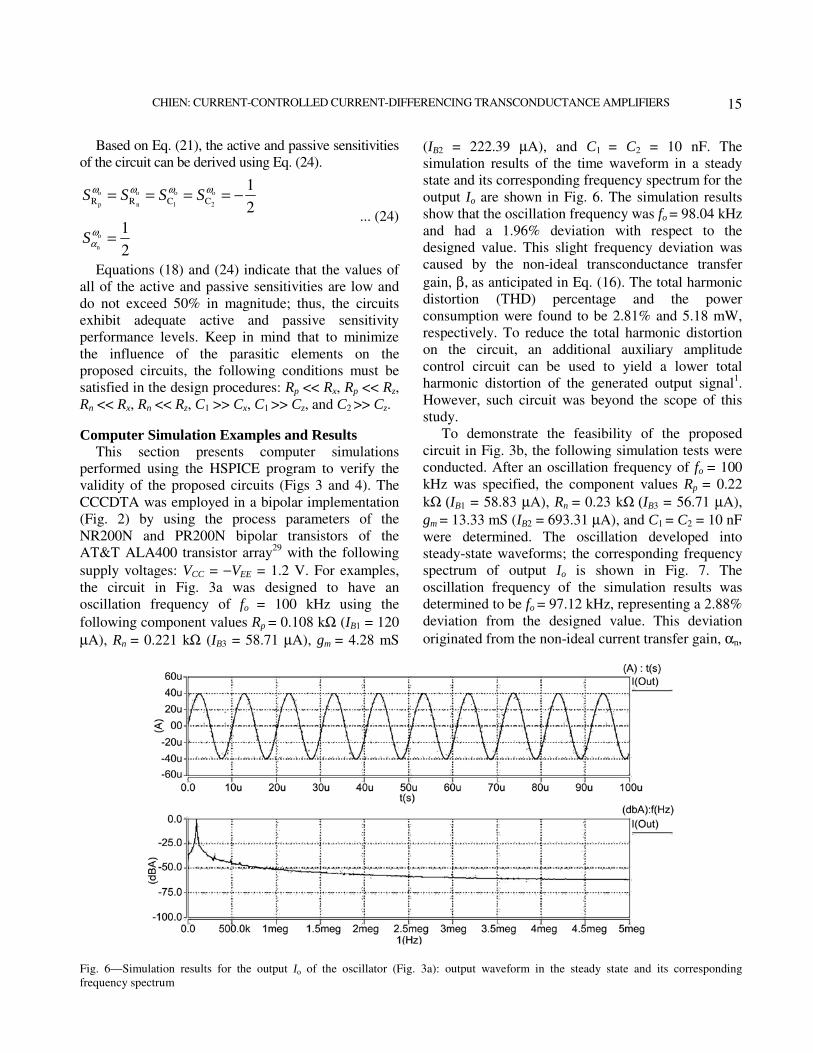
following component values Rp = 0.108 kΩ (IB1 = 120
µA), Rn = 0.221 kΩ (IB3 = 58.71 µA), gm = 4.28 mS
(IB2 = 222.39 µA), and C1 = C2 = 10 nF. The
simulation results of the time waveform in a steady
state and its corresponding frequency spectrum for the
output Io are shown in Fig. 6. The simulation results
show that the oscillation frequency was fo = 98.04 kHz
and had a 1.96% deviation with respect to the
designed value. This slight frequency deviation was
caused by the non-ideal transconductance transfer
gain, β, as anticipated in Eq. (16). The total harmonic
distortion (THD) percentage and the power
consumption were found to be 2.81% and 5.18 mW,
respectively. To reduce the total harmonic distortion
on the circuit, an additional auxiliary amplitude
control circuit can be used to yield a lower total
harmonic distortion of the generated output signal1.
However, such circuit was beyond the scope of this
study.
To demonstrate the feasibility of the proposed
circuit in Fig. 3b, the following simulation tests were
conducted. After an oscillation frequency of fo = 100
kHz was specified, the component values Rp = 0.22
kΩ (IB1 = 58.83 µA), Rn = 0.23 kΩ (IB3 = 56.71 µA),
gm = 13.33 mS (IB2 = 693.31 µA), and C1 = C2 = 10 nF
were determined. The oscillation developed into
steady-state waveforms; the corresponding frequency
spectrum of output Io is shown in Fig. 7. The
oscillation frequency of the simulation results was
determined to be fo = 97.12 kHz, representing a 2.88%
deviation from the designed value. This deviation
originated from the non-ideal current transfer gain, αn,
Fig. 6—Simulation results for the output Io of the oscillator (Fig. 3a): output waveform in the steady state and its corresponding
frequency spectrum
INDIAN J. ENG. MATER. SCI., FEBRUARY 2016
16
as anticipated in Eq. (21). The THD was 3.81% for
the current output, and the power consumption was
7.95 mW.
Because of the limitation of the CCCDTA maximal
slew rate, the highest oscillation frequency of the
circuits was limited; the following component values
were used for the circuit in Fig. 3a: Rp = 0.108 kΩ
(IB1 = 120 µA), Rn = 0.221 kΩ (IB3 = 58.71 µA),
gm = 1.15 mS (IB2 = 59.67 µA), and C1 = C2 = 0.1 nF.
Figure 8a shows the simulation results for the output
waveform of the circuit. The oscillation frequency
was recorded as fo = 4.93 MHz, indicating a 5.01%
frequency deviation from the theoretical calculation.
In consideration of the highest oscillation frequency
of the circuit in Fig. 3b, a specific simulation was
conducted using the component values Rp = 0.09
kΩ (IB1 = 145 µA), Rn = 0.23 kΩ (IB3 = 56.71 µA),
gm = 13.33 mS (IB2 = 693.31 µA), and C1 = C2 = 0.5
nF. The output waveform is shown in Fig. 8b. The
oscillation frequency was determined to be fo = 2.92
MHz, deviating from the theoretical value by 6.41%.
The simulation results (Fig. 8) indicated that the
highest oscillation frequency of the circuits occurred
at several megahertz.
Fig. 7—Simulation results for the output Io of the oscillator (Fig. 3b): output waveform in the steady state and its corresponding
frequency spectrum
Fig. 8—Simulation results for the highest applicable oscillations of the (a) oscillator in Fig. 3a and (b) oscillator in Fig. 3b
CHIEN: CURRENT-CONTROLLED CURRENT-DIFFERENCING TRANSCONDUCTANCE AMPLIFIERS
17
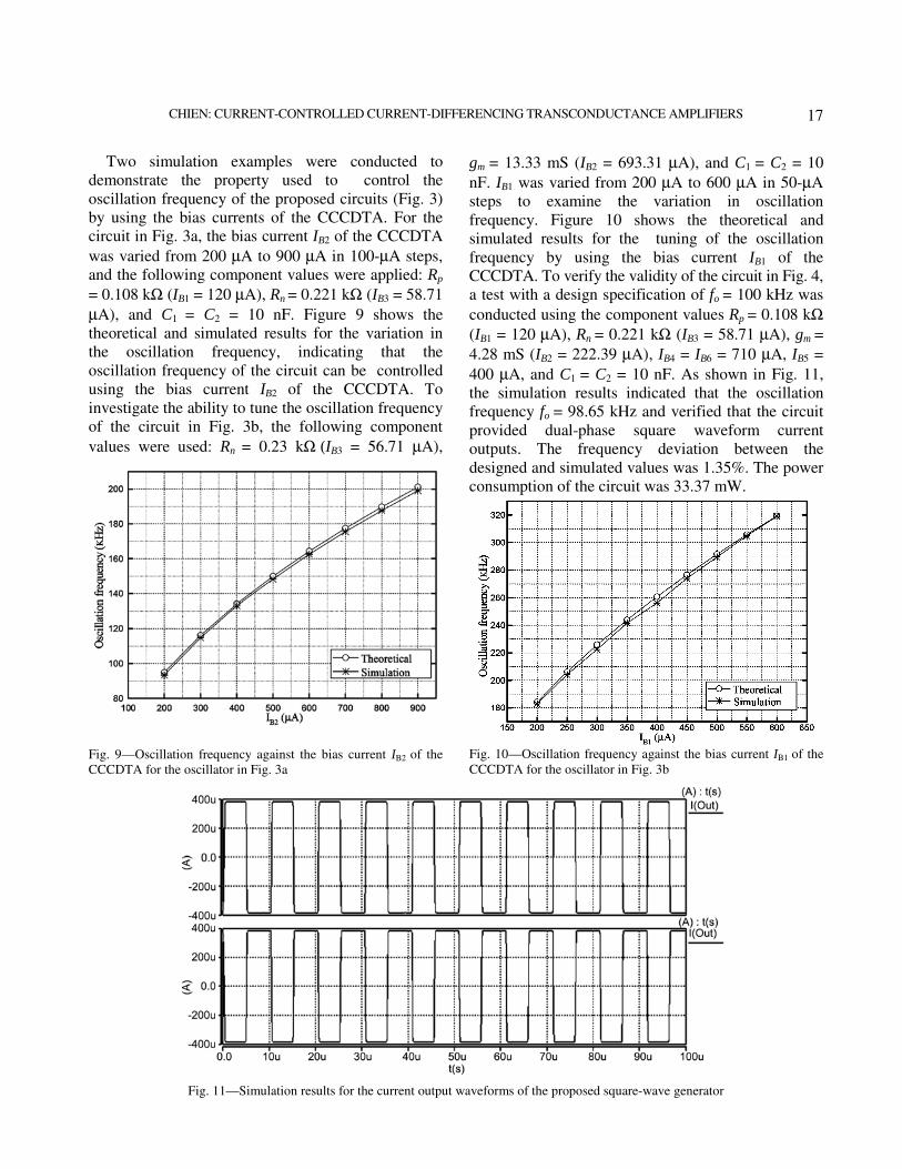
Two simulation examples were conducted to
demonstrate the property used to control the
oscillation frequency of the proposed circuits (Fig. 3)
by using the bias currents of the CCCDTA. For the
circuit in Fig. 3a, the bias current IB2 of the CCCDTA
was varied from 200 µA to 900 µA in 100-µA steps,
and the following component values were applied: Rp
= 0.108 kΩ (IB1 = 120 µA), Rn = 0.221 kΩ (IB3 = 58.71
µA), and C1 = C2 = 10 nF. Figure 9 shows the
theoretical and simulated results for the variation in
the oscillation frequency, indicating that the
oscillation frequency of the circuit can be controlled
using the bias current IB2 of the CCCDTA. To
investigate the ability to tune the oscillation frequency
of the circuit in Fig. 3b, the following component
values were used: Rn = 0.23 kΩ (IB3 = 56.71 µA),
gm = 13.33 mS (IB2 = 693.31 µA), and C1 = C2 = 10
nF. IB1 was varied from 200 µA to 600 µA in 50-µA
steps to examine the variation in oscillation
frequency. Figure 10 shows the theoretical and
simulated results for the tuning of the oscillation
frequency by using the bias current IB1 of the
CCCDTA. To verify the validity of the circuit in Fig. 4,
a test with a design specification of fo = 100 kHz was
conducted using the component values Rp = 0.108 kΩ
(IB1 = 120 µA), Rn = 0.221 kΩ (IB3 = 58.71 µA), gm =
4.28 mS (IB2 = 222.39 µA), IB4 = IB6 = 710 µA, IB5 =
400 µA, and C1 = C2 = 10 nF. As shown in Fig. 11,
the simulation results indicated that the oscillation
frequency fo = 98.65 kHz and verified that the circuit
provided dual-phase square waveform current
outputs. The frequency deviation between the
designed and simulated values was 1.35%. The power
consumption of the circuit was 33.37 mW.
Fig. 10—Oscillation frequency against the bias current IB1 of the
CCCDTA for the oscillator in Fig. 3b
Fig. 11—Simulation results for the current output waveforms of the proposed square-wave generator
Fig. 9—Oscillation frequency against the bias current IB2 of the
CCCDTA for the oscillator in Fig. 3a
INDIAN J. ENG. MATER. SCI., FEBRUARY 2016
18
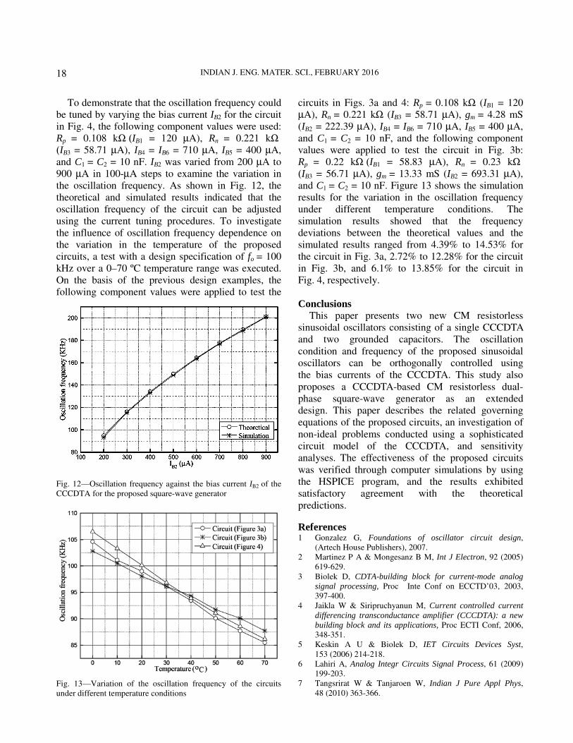
To demonstrate that the oscillation frequency could
be tuned by varying the bias current IB2 for the circuit
in Fig. 4, the following component values were used:
Rp = 0.108 kΩ (IB1 = 120 µA), Rn = 0.221 kΩ (IB3 = 58.71 µA), IB4 = IB6 = 710 µA, IB5 = 400 µA,
and C1 = C2 = 10 nF. IB2 was varied from 200 µA to
900 µA in 100-µA steps to examine the variation in
the oscillation frequency. As shown in Fig. 12, the
theoretical and simulated results indicated that the
oscillation frequency of the circuit can be adjusted
using the current tuning procedures. To investigate
the influence of oscillation frequency dependence on
the variation in the temperature of the proposed
circuits, a test with a design specification of fo = 100
kHz over a 0–70 ºC temperature range was executed.
On the basis of the previous design examples, the
following component values were applied to test the
circuits in Figs. 3a and 4: Rp = 0.108 kΩ (IB1 = 120
µA), Rn = 0.221 kΩ (IB3 = 58.71 µA), gm = 4.28 mS
(IB2 = 222.39 µA), IB4 = IB6 = 710 µA, IB5 = 400 µA,
and C1 = C2 = 10 nF, and the following component
values were applied to test the circuit in Fig. 3b:
Rp = 0.22 kΩ (IB1 = 58.83 µA), Rn = 0.23 kΩ (IB3 = 56.71 µA), gm = 13.33 mS (IB2 = 693.31 µA),
and C1 = C2 = 10 nF. Figure 13 shows the simulation
results for the variation in the oscillation frequency
under different temperature conditions. The
simulation results showed that the frequency
deviations between the theoretical values and the
simulated results ranged from 4.39% to 14.53% for
the circuit in Fig. 3a, 2.72% to 12.28% for the circuit
in Fig. 3b, and 6.1% to 13.85% for the circuit in
Fig. 4, respectively.
Conclusions
This paper presents two new CM resistorless
sinusoidal oscillators consisting of a single CCCDTA
and two grounded capacitors. The oscillation
condition and frequency of the proposed sinusoidal
oscillators can be orthogonally controlled using
the bias currents of the CCCDTA. This study also
proposes a CCCDTA-based CM resistorless dual-
phase square-wave generator as an extended
design. This paper describes the related governing
equations of the proposed circuits, an investigation of
non-ideal problems conducted using a sophisticated
circuit model of the CCCDTA, and sensitivity
analyses. The effectiveness of the proposed circuits
was verified through computer simulations by using
the HSPICE program, and the results exhibited
satisfactory agreement with the theoretical
predictions.
References 1 Gonzalez G, Foundations of oscillator circuit design,
(Artech House Publishers), 2007.
2 Martinez P A & Mongesanz B M, Int J Electron, 92 (2005)
619-629.
3 Biolek D, CDTA-building block for current-mode analog
signal processing, Proc Inte Conf on ECCTD’03, 2003,
397-400.
4 Jaikla W & Siripruchyanun M, Current controlled current
differencing transconductance amplifier (CCCDTA): a new
building block and its applications, Proc ECTI Conf, 2006,
348-351.
5 Keskin A U & Biolek D, IET Circuits Devices Syst,
153 (2006) 214-218.
6 Lahiri A, Analog Integr Circuits Signal Process, 61 (2009)
199-203.
7 Tangsrirat W & Tanjaroen W, Indian J Pure Appl Phys,
48 (2010) 363-366.
Fig. 12—Oscillation frequency against the bias current IB2 of the
CCCDTA for the proposed square-wave generator
Fig. 13—Variation of the oscillation frequency of the circuits
under different temperature conditions
CHIEN: CURRENT-CONTROLLED CURRENT-DIFFERENCING TRANSCONDUCTANCE AMPLIFIERS
19
8 Sakul C, Jaikla W & Dejhan K, Radioengineering, 20 (2011)
890-896.
9 Horng J W, Lee H & Wu J Y, Radioengineering, 19 (2010)
326-330.
10 Jaikla W, Siripruchyanun M, Bajer J & Biolek D,
Radioengineering, 17 (2008) 33-40.
11 Prasad D, Bhaskar D R & Singh A K, Radioengineering,
20 (2011) 354-359.
12 Jin J & Wang C, Int J Electron Commun, 66 (2012)
933-936.
13 Li Y, Radioengineering, 19 (2010) 667-671.
14 Summart S, Thongsopa C & Jaikla W, J Circuits Syst
Comput, 23 (2014) 15 pages.
15 Tangsrirat W, Indian J Eng Mater Sci, 14 (2007) 289-294.
16 Jaikla W & Lahiri A, Int J Electron Commun, 66 (2012)
214-218.
17 Tangsrirat W, Tanjaroen W & Pukkalanun T, Int J Electron
Commun, 63 (2009) 616-622.
18 Jaikla W & Prommee P, Radioengineering, 20 (2011)
594-599.
19 Prasad D, Bhaskar D R & Singh A K, WSEAS Trans
Electron, 5 (2008) 257-259.
20 Biolek D, Keskin A U & Biolkova V, IET Circuits Devices
Syst, 4 (2009) 496-502.
21 Chien H C & Wang J M, Microelectron J, 44 (2013)
216-224.
22 Filanovsky I M, Int J Electron, 72 (1992) 151-160.
23 Cicekoglu M O & Kuntman H, Microelectron J, 29 (1998)
983-989.
24 Srinivasulu A, Int J Circuit Theor Appl, 39 (2011)
679-686.
25 Marcellis A D, Carlo C D, Ferri G & Stornelli V,
Int J Circuit Theor Appl, 41 (2013) 1-13.
26 Hou C L, Chien H C & Lo Y K, IET Circuit Devices Syst,
152 (2005) 718-722.
27 Chien H C, Int J Electron, 100 (2013) 227-244.
28 P Silapan & M Siripruchyanun, Analog Integr Circuit Signal
Process, 68 (2011) 111-128.
29 D R Frey, IET Circuits Devices Syst, 140 (1993)
406-416.