shadow overlap ion-beam lithography vol. xx, no. x for
TRANSCRIPT

Shadow Overlap Ion-beam Lithographyfor NanoarchitecturesYeonho Choi,† Soongweon Hong,† and Luke P. Lee*
Biomolecular Nanotechnology Center, Berkeley Sensor and Actuator Center, Departmentof Bioengineering, UniVersity of California at Berkeley, Berkeley, California 94720
Received June 15, 2009; Revised Manuscript Received August 3, 2009
ABSTRACT
Precisely constructed nanoscale devices and nanoarchitectures with high spatial resolution are critically needed for applications in high-speed electronics, high-density memory, efficient solar cells, optoelectronics, plasmonics, optical antennas, chemical sensors, biologicalsensors, and nanospectroscopic imaging. Current methods of classical optical lithography are limited by the diffraction effect of light fornanolithography, and the state of art of e-beam or focused ion beam lithography limit the throughput and further reduction less than fewnanometers for large-area batch fabrication. However, these limits can be surpassed surprisingly by utilizing the overlap of two shadowimages. Here we present shadow overlap of ion-beam lithography (SOIL), which can combine the advantages of parallel processing, tunablecapability of geometries, cost-effective method, and high spatial resolution nanofabrication technique. The SOIL method relies on the overlapof shadows created by the directional metal deposition and etching angles on prepatterned structures. Consequently, highly tunable patternscan be obtained. As examples, unprecedented nanoarchitectures for optical antennas are demonstrated by SOIL. We expect that SOIL canhave a significant impact not only on nanoscale devices, but also large-scale (i.e., micro and macro) three-dimensional innovative lithography.
Noble metal nanostructures have received increasing interestin nanoscale electronics,1,2 photonics,2-7,12 plasmonics,2-13
and biotechnology3-6 due to their unique physical, optical,chemical, and mechanical properties, which can be tunedby the structure, material, and size.7 Consequently, thedevelopment of cost-effective, high-throughput, and tunablefabrication techniques are essential.
The standard lithography techniques include optical pho-tolithography,14,15 holographic lithography,16 electron beamlithography (EBL),17-19 and focused ion-beam lithography(FIB).20,21 However, since typical optical photolithographyis limited in its resolution due to the diffraction of light, itis necessary to overcome this limit without complicatedmethods such as immersion techniques, double patterning,or other nonlinear techniques.14 Although EBL and FIB allowthe fabrication of arbitrarily shaped nanostructures with highspatial resolution, the serial processing of these techniquesinherently shows serious challenges in high-throughput andis responsible for their high cost. Nanosphere lithography(NSL),22-25 laser interference lithography (LIL),25,26 andshadow-based nanofabrication27,28 can be good alternativeparallel and low-cost lithography methods, but in generalthese techniques are seriously limited to specific fabricatedshapes such as prisms and disks.
Here, we present the shadow overlap of ion-beam lithog-raphy (SOIL), which is a tunable and parallel nanolitho-
graphic method. It is based on simple prepatterned micro/nanostructure arrays, shadows, and overlaps between shadowsobtained by the angle of metal deposition using directionale-beam evaporation or ion-beam milling. This technique canprovide several benefits to overcome the limitations of thepreviously described systems. First, this method has poten-tially a single digit of nanoscale spatial resolution since thenanostructures are fabricated by using the shadow area ofprepatterned structures, which are generated by the direc-tional metal layer deposition and etching. For example, abow-tie structure with a gap of 10 nm or less is easilyachieved with this lithographic technique (Figure 2a).Second, we can make many different shapes of nanostructurearrays, since the shadow shape or area can be changed withdifferent prepatterned structures, the angle of metal depositionand etching, or the number of deposition cycles. Third, thistechnique allows batch nanofabrication; we can fabricate thesame nanostructure in arrays over a large-area at one time.Fourth, SOIL is a relatively simple and cost-effective method.
The general concept of SOIL is illustrated schematicallyin Figure 1a. A metal layer is deposited with a specific angleon the substrate. As expected, metal is selectively coveredon the surface of the substrate due to the shadows createdby the angle of deposition and prepatterned structure.Because of the regular prepatterned array, a shadow of onestructure can overlap the neighboring structure, and the metaldeposited area becomes different from that of a singlestructure due to the shadow-structure overlap. Analogous tothe angled deposition result, directional ion-beam etching
* To whom correspondence should be addressed. E-mail: [email protected]. Phone: (510)642-5855.
† Equally contributed to this work.
NANOLETTERS
XXXXVol. xx, No. x
-
10.1021/nl901911p CCC: $40.75 XXXX American Chemical Society
Dow
nloa
ded
by U
OF
CA
LIF
OR
NIA
BE
RK
EL
EY
on
Sept
embe
r 15
, 200
9 | h
ttp://
pubs
.acs
.org
P
ublic
atio
n D
ate
(Web
): S
epte
mbe
r 15
, 200
9 | d
oi: 1
0.10
21/n
l901
911p

can remove metal layer except where a shadow is cast. Thefinal nanostructure remains in the shadowed area and has acompletely different shape compared to the conventionallyfabricated nanostructure using angle deposition and etchingbecause of the shadow-structure overlap. Moreover, a varietyof nanostructure shapes can be fabricated by controlling thekey factors, which are the zenith angle (i.e., the angle fromthe normal direction on the substrate to the deposition oretching direction in the cross-section view), the number ofdeposition or etching cycles, and the azimuth angle (i.e., theangle between the crystal line of the prepatterned array andthe directions of the deposition and etching in the top view)(Figure 1b)
As a demonstration, polystyrene (PS) beads were selectedas prepattern array for several reasons. (i) The selectivity
and uniformity in size; from tens of nanometers to severalmicrometers, PS beads have a wide range in size and a highlyuniform distribution in each size. (ii) Large-area uniformpattern; it is critical to get a uniform prepattern in a large-area to fabricate highly uniform nanostructures array bySOIL. As reported in many literatures, large-area, uniform,closed-packed patterning (over 1 cm2) has been accom-plished.24,29,30 (iii) Size tunability by isotropic dry etching;the size is easily controlled by oxygen plasma etching (i.e.,isotropic etching) while its shape remains a sphere. Conse-quently, the interparticle distance in the array can becontrolled, which is one of the key factors of SOIL.
The transparency of the substrate is important for opticalcharacterization of the fabricated SOIL pattern and futureapplications in optics. In order to satisfy this prerequisite, amicroscope glass slide was selected as a substrate. Surfactant-free carboxyl-terminated PS nanospheres with a diameter of477 nm were self-assembled on top of the glass substrateby using a drop-casting method (Supporting InformationFigure S1I). Because the capability to fabricate various typesof nanostructures by SOIL comes from the shadows and theoverlap of the shadows induced by the directional metaldeposition and etching, PS beads were isotropically etchedwith oxygen plasma to reduce their size by 85% (i.e., 405nm in diameter) thus making space between them (Support-ing Information Figure S1 II). Twenty nanometers of goldwas directionally deposited with zenith angles of 10, 20, 30,and 40° based on the normal direction to the substrate(Supporting Information Figure S1 III). During depositions,gold was covered on a glass substrate except in the shadowarea created by PS beads. Since this shadow is dependenton the deposition angle, the gold-patterned area is changedby the zenith angle also. A directional dry etching by ion-beam milling was applied to remove the gold film. Whilethe etching was in progress, the shadows protected the goldstructure (Supporting Information Figure S1 IV and V). Theoverlap of the deposition and etching shadows with hexago-nally patterned PS bead array allowed us to generate manydifferent nanostructure patterns.
We investigated fabricating nanostructures by SOIL as afunction of the gold deposition angle and the number ofdeposition times. The zenith angle of ion-beam milling wasfixed at 0°, which was the normal direction on the substrate.In the top view, the azimuth angle is one of the keyfabrication parameters. Since the drop-casting method wasused to obtain PS bead arrays in this work, PS bead arraysat each grain boundary showed different directions. However,as representative examples, we show two extreme casesnamed “matching” and “mis-matching”, which indicates thecases of the minimum and maximum (i.e., 0 and 30°,respectively) azimuth angle (Figure 2). At low zenith angle,a nanocrescent array was fabricated regardless azimuth angle.In this regime, no advantage of SOIL can be obtainedbecause there is no shadow overlap effect. However, as thezenith angle of the gold deposition increased, the metaldeposition shadows from the neighboring PS beads startedinterfering with the etching shadow (i.e., the overlap ofdeposition and etching shadow). As a result, many different
Figure 1. The schematics and representative patterns by SOIL. (a)Schematic diagrams of the representative patterns based on spheresand cylinders. (b) Illustration of the representative nanostructures (left,nanobulls; right, nanodouble axes) by SOIL using PS nanospherearrays, and corresponding SEM images. (c) The schematic and SEMimages of the fabricated nanoarchitecture by SOIL using pillar array.The scale bar corresponds 500 nm.
B Nano Lett., Vol. xx, No. x, XXXX
Dow
nloa
ded
by U
OF
CA
LIF
OR
NIA
BE
RK
EL
EY
on
Sept
embe
r 15
, 200
9 | h
ttp://
pubs
.acs
.org
P
ublic
atio
n D
ate
(Web
): S
epte
mbe
r 15
, 200
9 | d
oi: 1
0.10
21/n
l901
911p
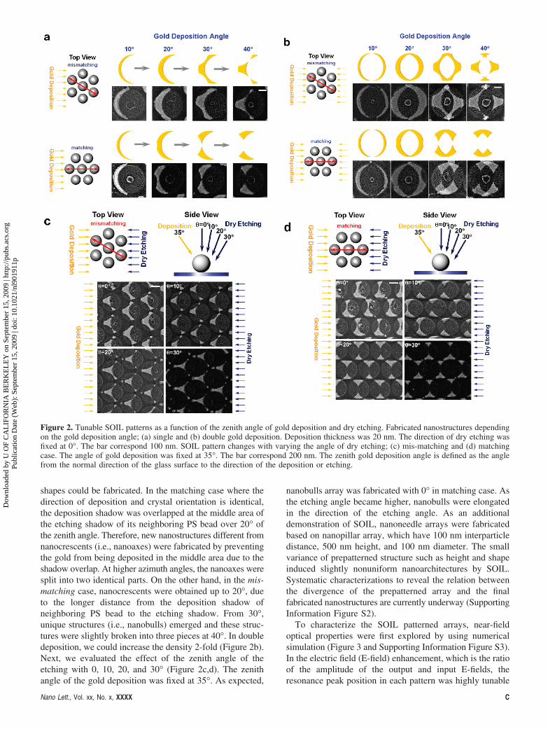
shapes could be fabricated. In the matching case where thedirection of deposition and crystal orientation is identical,the deposition shadow was overlapped at the middle area ofthe etching shadow of its neighboring PS bead over 20° ofthe zenith angle. Therefore, new nanostructures different fromnanocrescents (i.e., nanoaxes) were fabricated by preventingthe gold from being deposited in the middle area due to theshadow overlap. At higher azimuth angles, the nanoaxes weresplit into two identical parts. On the other hand, in the mis-matching case, nanocrescents were obtained up to 20°, dueto the longer distance from the deposition shadow ofneighboring PS bead to the etching shadow. From 30°,unique structures (i.e., nanobulls) emerged and these struc-tures were slightly broken into three pieces at 40°. In doubledeposition, we could increase the density 2-fold (Figure 2b).Next, we evaluated the effect of the zenith angle of theetching with 0, 10, 20, and 30° (Figure 2c,d). The zenithangle of the gold deposition was fixed at 35°. As expected,
nanobulls array was fabricated with 0° in matching case. Asthe etching angle became higher, nanobulls were elongatedin the direction of the etching angle. As an additionaldemonstration of SOIL, nanoneedle arrays were fabricatedbased on nanopillar array, which have 100 nm interparticledistance, 500 nm height, and 100 nm diameter. The smallvariance of prepatterned structure such as height and shapeinduced slightly nonuniform nanoarchitectures by SOIL.Systematic characterizations to reveal the relation betweenthe divergence of the prepatterned array and the finalfabricated nanostructures are currently underway (SupportingInformation Figure S2).
To characterize the SOIL patterned arrays, near-fieldoptical properties were first explored by using numericalsimulation (Figure 3 and Supporting Information Figure S3).In the electric field (E-field) enhancement, which is the ratioof the amplitude of the output and input E-fields, theresonance peak position in each pattern was highly tunable
Figure 2. Tunable SOIL patterns as a function of the zenith angle of gold deposition and dry etching. Fabricated nanostructures dependingon the gold deposition angle; (a) single and (b) double gold deposition. Deposition thickness was 20 nm. The direction of dry etching wasfixed at 0°. The bar correspond 100 nm. SOIL pattern changes with varying the angle of dry etching; (c) mis-matching and (d) matchingcase. The angle of gold deposition was fixed at 35°. The bar correspond 200 nm. The zenith gold deposition angle is defined as the anglefrom the normal direction of the glass surface to the direction of the deposition or etching.
Nano Lett., Vol. xx, No. x, XXXX C
Dow
nloa
ded
by U
OF
CA
LIF
OR
NIA
BE
RK
EL
EY
on
Sept
embe
r 15
, 200
9 | h
ttp://
pubs
.acs
.org
P
ublic
atio
n D
ate
(Web
): S
epte
mbe
r 15
, 200
9 | d
oi: 1
0.10
21/n
l901
911p
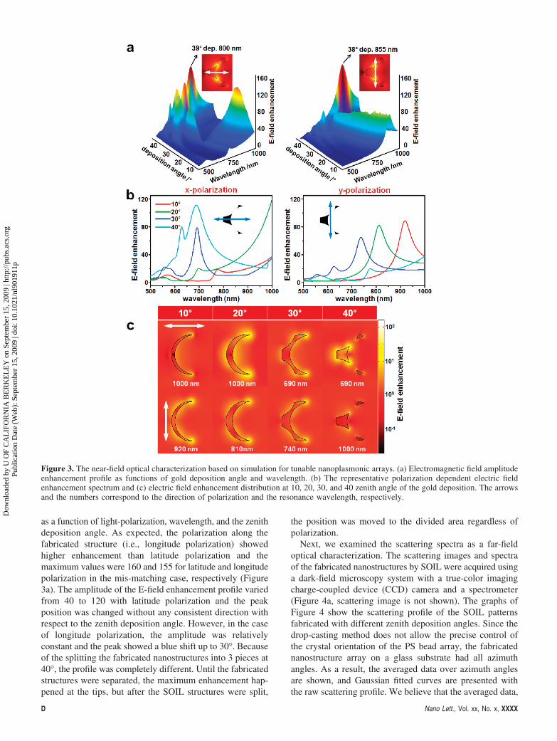
as a function of light-polarization, wavelength, and the zenithdeposition angle. As expected, the polarization along thefabricated structure (i.e., longitude polarization) showedhigher enhancement than latitude polarization and themaximum values were 160 and 155 for latitude and longitudepolarization in the mis-matching case, respectively (Figure3a). The amplitude of the E-field enhancement profile variedfrom 40 to 120 with latitude polarization and the peakposition was changed without any consistent direction withrespect to the zenith deposition angle. However, in the caseof longitude polarization, the amplitude was relativelyconstant and the peak showed a blue shift up to 30°. Becauseof the splitting the fabricated nanostructures into 3 pieces at40°, the profile was completely different. Until the fabricatedstructures were separated, the maximum enhancement hap-pened at the tips, but after the SOIL structures were split,
the position was moved to the divided area regardless ofpolarization.
Next, we examined the scattering spectra as a far-fieldoptical characterization. The scattering images and spectraof the fabricated nanostructures by SOIL were acquired usinga dark-field microscopy system with a true-color imagingcharge-coupled device (CCD) camera and a spectrometer(Figure 4a, scattering image is not shown). The graphs ofFigure 4 show the scattering profile of the SOIL patternsfabricated with different zenith deposition angles. Since thedrop-casting method does not allow the precise control ofthe crystal orientation of the PS bead array, the fabricatednanostructure array on a glass substrate had all azimuthangles. As a result, the averaged data over azimuth anglesare shown, and Gaussian fitted curves are presented withthe raw scattering profile. We believe that the averaged data,
Figure 3. The near-field optical characterization based on simulation for tunable nanoplasmonic arrays. (a) Electromagnetic field amplitudeenhancement profile as functions of gold deposition angle and wavelength. (b) The representative polarization dependent electric fieldenhancement spectrum and (c) electric field enhancement distribution at 10, 20, 30, and 40 zenith angle of the gold deposition. The arrowsand the numbers correspond to the direction of polarization and the resonance wavelength, respectively.
D Nano Lett., Vol. xx, No. x, XXXX
Dow
nloa
ded
by U
OF
CA
LIF
OR
NIA
BE
RK
EL
EY
on
Sept
embe
r 15
, 200
9 | h
ttp://
pubs
.acs
.org
P
ublic
atio
n D
ate
(Web
): S
epte
mbe
r 15
, 200
9 | d
oi: 1
0.10
21/n
l901
911p

white light excitation (i.e., unpolarized light), and inherentdifference of near-field and far-field optical characteristiccould make slightly the different results between simulationand experiment. The scattering spectra had a major singlepeak which existed in the range from 580 to 680 nm. As thezenith deposition angle increased, the scattering peaksconsistently increased (i.e., red-shifted) in the single deposi-tion case. On the other hand, in the case of double deposition,the peak position shifts to longer wavelengths up to 30° ofthe deposition angle; however, after 30°, it became blueshifted.
In conclusion, we have demonstrated a cost-effective, high-throughput, and tunable lithography method with high spatialresolution by the shadow overlap from the directional metaldeposition and etching in prepatterned polystyrene arrays.We found that various types of nanostructure arrays couldbe easily fabricated in large areas by changing the zenithand azimuth angle of the metal deposition and etching andthe number of metal deposition times. Moreover, tunable anduniform nanostructure arrays with high spatial resolution suchas bow-tie shape with 10 nm gap or modified crescent shapewere achieved in parallel processing by SOIL. The fabricatedstructures showed high electromagnetic (EM) field enhance-ment and polarization dependent EM field distributions inthe near-field, and the scattering peak position was tuned asa function of the deposition angle. Since it is obvious thatdifferent prepatterned arrays such as pillars or pyramids cangenerate completely different shapes by overlapping twoshadows, this lithographic method can potentially be ex-tended to fabricate a wide variety of nanostructure arrayswith different prepatterned arrays. We believe that our SOILmethod will have major impacts on the fields of photonics,nanoelectronics, and future quantitative chemical or biomo-lecular sensing.
Acknowledgment. We thank Liz Y. Wu for metaldeposition. This work is supported by DARPA SERS S&TFundamental Program under LLNL (Code No. B573237),DARPA MF3 (Award No. HR0011-06-1-0050) and Centerfor Nanostructured Materials and Technology (CNMT) underthe 21st Century Frontier Research Programs of the Koreagovernment.
Supporting Information Available: Fabrication method,Ordered pillar array based SOIL pattern, Further simulationresults. This material is available free of charge via theInternet at http://pubs.acs.org.
References(1) Cui, Y.; Lieber, C. M. Science 2001, 291, 851–853.(2) Ozbay, E. Science 2006, 311, 189–193.(3) Barnes, W. L.; Dereux, A.; Ebbesen, T. W. Nature 2003, 424, 824–
830.(4) Alivisatos, P. Nat. Biotechnol. 2004, 22, 47–52.(5) Anker, J. N.; et al. Nat. Mater. 2008, 7, 442–453.(6) Rosi, N. L.; Mirkin, C. A. Chem. ReV. 2005, 105, 1547–1562.(7) Bohren, C. F.; Huffman, D. R. Absorption and scattering of light by
small particles; Wiley: New York: 1983.(8) Jackson, J. B.; Halas, N. J. Proc. Natl. Acad. Sci. U.S.A. 2004, 101,
17930–17935.(9) Lu, Y.; et al. Nano Lett. 2005, 5, 119–124.
(10) Liu, G. L.; et al. AdV. Mater. 2005, 17, 2683–2688.(11) Choi, D.; et al. Lab Chip 2009, 9, 239–243.
Figure 4. The far-field optical characterization for the fabricatedSOIL pattern arrays. (a) The experimental configuration and themeasured extinction coefficients as a function of gold depositionangle at (b) 10, (c) 20, (d) 30, and (e) 40° (left, single deposition;right, double deposition). (f) Rayleigh scattering resonance peakchange.
Nano Lett., Vol. xx, No. x, XXXX E
Dow
nloa
ded
by U
OF
CA
LIF
OR
NIA
BE
RK
EL
EY
on
Sept
embe
r 15
, 200
9 | h
ttp://
pubs
.acs
.org
P
ublic
atio
n D
ate
(Web
): S
epte
mbe
r 15
, 200
9 | d
oi: 1
0.10
21/n
l901
911p

(12) Liu, G. L.; et al. Nat. Methods 2007, 4, 1015–1017.(13) Choi, Y.; et al. Nano Lett. 2009, 9, 85–90.(14) Takashi, I.; Okazaki, S. Nature 2000, 406, 1027–1031.(15) Moreau, W. M. Semiconductor Lithography: principles and materials;
Plenum: New York, 1988.(16) Campbell, M.; et al. Nature 2000, 404, 53–56.(17) Craighead, H. G.; et al. Appl. Phys. Lett. 1983, 42, 38–40.(18) Quake, S. R.; Scherer, A. Science 2000, 290, 1536–1540.(19) Haynes, C. L.; et al. J. Phys. Chem. B 2003, 107, 7337–7342.(20) Tong, H. D.; et al. Nano Lett. 2004, 4, 283–287.(21) Li, J.; et al. Nature 2001, 412, 166–169.
(22) Jensen, T. R.; et al. J. Phys. Chem. B 2000, 104, 10549–10556.(23) Whitney, A. V.; et al. Nano Lett. 2004, 4, 1507–1511.(24) Kosiorek, A.; et al. Nano Lett. 2004, 4, 1359–1363.(25) Vogelaar, L.; et al. AdV. Mater. 2001, 13, 1551–1554.(26) Zheng, M.; et al. Appl. Phy. Lett. 2001, 79, 2606–2608.(27) Douglas, K.; Devaud, G.; Clark, N. A. Science 1992, 257, 642–64.(28) Philipp, G.; et al. Microelectron. Eng. 1999, 46, 157–160.(29) Kempa, K. Nano Lett. 2003, 3, 13–18.(30) Hsu, C. M.; et al. Appl. Phys. Lett. 2008, 93, 133109.
NL901911P
F Nano Lett., Vol. xx, No. x, XXXX
Dow
nloa
ded
by U
OF
CA
LIF
OR
NIA
BE
RK
EL
EY
on
Sept
embe
r 15
, 200
9 | h
ttp://
pubs
.acs
.org
P
ublic
atio
n D
ate
(Web
): S
epte
mbe
r 15
, 200
9 | d
oi: 1
0.10
21/n
l901
911p