semiconductor device modeling and characterization – ee5342 lecture 7 – spring 2011
DESCRIPTION
Semiconductor Device Modeling and Characterization – EE5342 Lecture 7 – Spring 2011. Professor Ronald L. Carter [email protected] http://www.uta.edu/ronc/. First Assignment. e-mail to [email protected] In the body of the message include subscribe EE5342 - PowerPoint PPT PresentationTRANSCRIPT

Semiconductor Device Modeling and
Characterization – EE5342 Lecture 7 – Spring 2011
Professor Ronald L. [email protected]
http://www.uta.edu/ronc/

©rlc L07-07Feb2011
2
First Assignment
• e-mail to [email protected]– In the body of the message include
subscribe EE5342 • This will subscribe you to the
EE5342 list. Will receive all EE5342 messages
• If you have any questions, send to [email protected], with EE5342 in subject line.

©rlc L07-07Feb2011
3
Second Assignment
• Submit a signed copy of the document that is posted at
www.uta.edu/ee/COE%20Ethics%20Statement%20Fall%2007.pdf

©rlc L07-07Feb2011
4
Schedule Changes Due to the University Closures last week• Plan to meet until noon some days in the next few weeks. This way we will make up the lost time. The first extended class will be Wednesday, February 9.
• The MT will be postponed until Wednesday, February 16. All other due dates and tests will remain the same.

©rlc L07-07Feb2011
5
Equipartitiontheorem• The thermodynamic energy per
degree of freedom is kT/2Consequently,
sec/cm10*m
kT3v
and ,kT23
vm21
7rms
thermal2

©rlc L07-07Feb2011
6
Carrier velocitysaturation1
• The mobility relationship v = mE is limited to “low” fields
• v < vth = (3kT/m*)1/2 defines “low”
• v = moE[1+(E/Ec)b]-1/b, mo = v1/Ec for Si
parameter electrons holes v1 (cm/s) 1.53E9 T-0.87 1.62E8 T-
0.52
Ec (V/cm) 1.01 T1.55 1.24 T1.68
b 2.57E-2 T0.66 0.46 T0.17

©rlc L07-07Feb2011
7
vdrift [cm/s] vs. E [V/cm] (Sze2, fig. 29a)
©rlc L07-07Feb2011
8
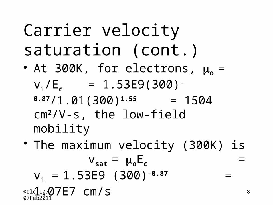
Carrier velocitysaturation (cont.)• At 300K, for electrons, mo = v1/Ec
= 1.53E9(300)-
0.87/1.01(300)1.55 = 1504 cm2/V-s, the low-field mobility
• The maximum velocity (300K) is vsat = moEc
= v1 =
1.53E9 (300)-0.87 = 1.07E7 cm/s

©rlc L07-07Feb2011
9
Diffusion ofcarriers• In a gradient of electrons or holes, p and n are not zero
• Diffusion current,`J =`Jp +`Jn (note Dp and Dn are diffusion coefficients)
kji
kji
zn
yn
xn
qDnqDJ
zp
yp
xp
qDpqDJ
nnn
ppp

©rlc L07-07Feb2011
10
Diffusion ofcarriers (cont.)• Note (p)x has the magnitude of
dp/dx and points in the direction of increasing p (uphill)
• The diffusion current points in the direction of decreasing p or n (downhill) and hence the - sign in the definition of`Jp and the + sign in the definition of`Jn

©rlc L07-07Feb2011
11
Diffusion ofCarriers (cont.)

©rlc L07-07Feb2011
12
Current densitycomponents
nqDJ
pqDJ
VnqEnqEJ
VpqEpqEJ
VE since Note,
ndiffusion,n
pdiffusion,p
nnndrift,n
pppdrift,p

©rlc L07-07Feb2011
13
Total currentdensity
nqDpqDVJ
JJJJJ
gradient
potential the and gradients carrier the
by driven is density current total The
npnptotal
.diff,n.diff,pdrift,ndrift,ptotal

©rlc L07-07Feb2011
14
Doping gradient induced E-field• If N = Nd-Na = N(x), then so is Ef-Efi
• Define f = (Ef-Efi)/q = (kT/q)ln(no/ni)
• For equilibrium, Efi = constant, but• for dN/dx not equal to zero, • Ex = -df/dx =- [d(Ef-Efi)/dx](kT/q)
= -(kT/q) d[ln(no/ni)]/dx= -(kT/q) (1/no)
[dno/dx] = -(kT/q) (1/N)[dN/dx], N > 0

©rlc L07-07Feb2011
15
Induced E-field(continued)• Let Vt = kT/q, then since
• nopo = ni2 gives no/ni = ni/po
• Ex = - Vt d[ln(no/ni)]/dx= - Vt d[ln(ni/po)]/dx
= - Vt d[ln(ni/|N|)]/dx, N = -Na < 0
• Ex = - Vt (-1/po)dpo/dx = Vt(1/po)dpo/dx
= Vt(1/Na)dNa/dx
©rlc L07-07Feb2011
16
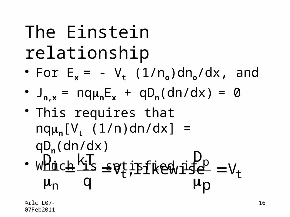
The Einsteinrelationship• For Ex = - Vt (1/no)dno/dx, and
• Jn,x = nqmnEx + qDn(dn/dx) = 0• This requires that
nqmn[Vt (1/n)dn/dx] = qDn(dn/dx)
• Which is satisfied ift
pt
n
n Vp
D likewise ,V
qkTD

©rlc L07-07Feb2011
17
Direct carriergen/recomb
gen rec
-
+ +
-
Ev
Ec
Ef
Efi
E
k
Ec
Ev
(Excitation can be by light)

©rlc L07-07Feb2011
18
Direct gen/recof excess carriers• Generation rates, Gn0 = Gp0
• Recombination rates, Rn0 = Rp0
• In equilibrium: Gn0 = Gp0 = Rn0 = Rp0
• In non-equilibrium condition:n = no + dn and p = po + dp, where
nopo=ni2
and for dn and dp > 0, the recombination rates increase to R’n and R’p

©rlc L07-07Feb2011
19
Direct rec forlow-level injection• Define low-level injection as
dn = dp < no, for n-type, and dn = dp < po, for p-type
• The recombination rates then areR’n = R’p = dn(t)/tn0, for p-
type, and R’n = R’p = dp(t)/tp0, for n-type
• Where tn0 and tp0 are the minority-carrier lifetimes

©rlc L07-07Feb2011
20
Shockley-Read-Hall Recomb
Ev
Ec
Ef
Efi
E
k
Ec
Ev
ET
Indirect, like Si, so intermediate state

©rlc L07-07Feb2011
21
S-R-H trapcharacteristics1
• The Shockley-Read-Hall Theory requires an intermediate “trap” site in order to conserve both E and p
• If trap neutral when orbited (filled) by an excess electron - “donor-like”
• Gives up electron with energy Ec - ET
• “Donor-like” trap which has given up the extra electron is +q and “empty”

©rlc L07-07Feb2011
22
S-R-H trapchar. (cont.)• If trap neutral when orbited (filled)
by an excess hole - “acceptor-like” • Gives up hole with energy ET - Ev
• “Acceptor-like” trap which has given up the extra hole is -q and “empty”
• Balance of 4 processes of electron capture/emission and hole capture/ emission gives the recomb rates

©rlc L07-07Feb2011
23
References *Fundamentals of Semiconductor Theory and
Device Physics, by Shyh Wang, Prentice Hall, 1989.
**Semiconductor Physics & Devices, by Donald A. Neamen, 2nd ed., Irwin, Chicago.
M&K = Device Electronics for Integrated Circuits, 3rd ed., by Richard S. Muller, Theodore I. Kamins, and Mansun Chan, John Wiley and Sons, New York, 2003.
• 1Device Electronics for Integrated Circuits, 2 ed., by Muller and Kamins, Wiley, New York, 1986.
• 2Physics of Semiconductor Devices, by S. M. Sze, Wiley, New York, 1981.
• 3 Physics of Semiconductor Devices, Shur, Prentice-Hall, 1990.