section 27. usb on-the-go (otg)ww1.microchip.com/downloads/en/devicedoc/61126f.pdf · section 27....
TRANSCRIPT

Section 27. USB On-The-Go (OTG)
USB
On-The-G
o (O
TG)
27
HIGHLIGHTSThis section of the manual contains the following major topics:
27.1 Introduction .................................................................................................................. 27-227.2 Control Registers ......................................................................................................... 27-427.3 Operation ................................................................................................................... 27-3627.4 Host Mode Operation................................................................................................. 27-5127.5 Interrupts.................................................................................................................... 27-5927.6 I/O Pins ...................................................................................................................... 27-6227.7 Operation in Debug and Power-Saving Modes.......................................................... 27-6427.8 Effects of a Reset....................................................................................................... 27-6627.9 Related Application Notes.......................................................................................... 27-67
© 2011 Microchip Technology Inc. DS61126F-page 27-1
PIC32 Family Reference Manual
27.1 INTRODUCTIONThe PIC32 USB OTG module includes the following features:
• USB Full-Speed Support for Host and Device• Low-Speed Host Support• USB On-The-Go (OTG) Support• Integrated Signaling Resistors• Integrated Analog Comparators for VBUS Monitoring• Integrated USB Transceiver• Transaction Handshaking Performed by Hardware• Endpoint Buffering Anywhere in System RAM• Integrated Bus Master to Access System RAM and Flash• USB OTG module does not require the PIC32 DMA module for its operation
The USB OTG module contains analog and digital components to provide a USB 2.0 full-speedand low-speed embedded host, full-speed device, or OTG implementation with a minimum ofexternal components. This module in Host mode is intended for use as an embedded host andtherefore does not implement a UHCI or OHCI controller.
The USB OTG module consists of the clock generator, the USB voltage comparators, the trans-ceiver, the Serial Interface Engine (SIE), a dedicated USB Bus Master, pull-up and pull-downresistors and the register interface. A block diagram of the USB OTG module is presented inFigure 27-1.
The clock generator provides the 48 MHz clock, which is required for USB full-speed andlow-speed communication. The voltage comparators monitor the voltage on the VBUS pin todetermine the state of the bus. The transceiver provides the analog translation between the USBbus and the digital logic. The SIE is a state machine that transfers data to and from the endpointbuffers, and generates the hardware protocol for data transfers. The USB Bus Master transfersdata between the data buffers in RAM and the SIE. The integrated pull-up and pull-down resistorseliminate the need for external signaling components. The register interface allows the CPU toconfigure and communicate with the module.
Note: This family reference manual section is meant to serve as a complement to devicedata sheets. Depending on the device variant, this manual section may not apply toall PIC32 devices.
Please consult the note at the beginning of the “USB On-The-Go (OTG)” chapterin the current device data sheet to check whether this document supports the deviceyou are using.
Device data sheets and family reference manual sections are available fordownload from the Microchip Worldwide Web site at: http://www.microchip.com
IMPORTANT: The implementation and use of the USB specifications, as well as otherthird-party specifications or technologies, may require licensing; including,but not limited to, USB Implementers Forum, Inc. (also referred to asUSB-IF). The user is fully responsible for investigating and satisfying anyapplicable licensing obligations.
DS61126F-page 27-2 © 2011 Microchip Technology Inc.

Section 27. USB On-The-Go (OTG)U
SB O
n-The-Go
(OTG
)
27
Figure 27-1: PIC32 USB OTG Interface Diagram
Note 1: PB clock is only available on this pin for select EC modes.2: Pins can be used as digital inputs when USB is not enabled.3: This bit field is contained in the OSCCON register.4: This bit field is contained in the OSCTRM register.5: USB PLL UFIN requirements: 4 MHz ≤ UFIN ≤ 5 MHz.6: This bit field is contained in the DEVCFG2 register.7: A 48 MHz clock is required for proper USB operation.8: Pins can be used as GPIO when the USB OTG module is disabled.9: Pin is pulled high internally when USB OTG module is enabled.
OSC1
OSC2
Primary Oscillator
8 MHz Typical
FRCOscillator
TUN<5:0>(4)
PLL
48 MHz USB Clock(7)
Div x
UPLLEN(6)
(PBOUT)(1)
UFRCEN(3)
(POSC)
FUPLLIDIV(6)
UFIN(5)
Div 2
VUSB
D+(2)
D-(2)
ID(8,9)
VBUS
Transceiver
SIE
VBUSON(8)
Comparators
USBSRP Charge
SRP Discharge
Registersand
ControlInterface
Transceiver Power 3.3V
To Clock Generator for Core and Peripherals
Sleep or Idle
Sleep
USBEN
USB Suspend
CPU Clock Not POSC
USB OTG Module
Voltage
SystemRAM
USB Suspend
Full-Speed Pull-up
Host Pull-down
Low-Speed Pull-up
Host Pull-down
ID Pull-up
Bus Master
24xPLL
© 2011 Microchip Technology Inc. DS61126F-page 27-3

PIC32 Family Reference Manual
27.2 CONTROL REGISTERSThe USB OTG module includes the following Special Function Registers (SFRs):
• U1OTGIR: USB OTG Interrupt Status RegisterThis register records changes on the ID, data and VBUS pins, enabling software to determinewhich event caused an interrupt. The interrupt bits are cleared by writing a ‘1’ to the correspondinginterrupt.
• U1OTGIE: USB OTG Interrupt Enable RegisterThis register enables the corresponding interrupt status bits defined in the U1OTGIR registerto generate an interrupt.
• U1OTGSTAT: USB OTG Status RegisterThis register provides access to the status of the VBUS voltage comparators and thedebounced status of the ID pin.
• U1OTGCON: USB OTG Control RegisterThis register controls the operation of the VBUS pin, and the pull-up and pull-down resistors.
• U1PWRC: USB Power Control RegisterThis register controls the power-saving modes, as well as the module enable/disablecontrol.
• U1IR: USB Interrupt RegisterThis register contains information on pending interrupts. Once an interrupt bit is set, it canbe cleared by writing a ‘1’ to the corresponding bit.
• U1IE: USB Interrupt Enable Register(1)
The values in this register provide gating of the various interrupt signals onto the USB inter-rupt signal. These values do not interact with the USB OTG module. Setting any of thesebits enables the corresponding interrupt source in the U1IR register.
• U1EIR: USB Error Interrupt Status RegisterThis register contains information on pending error interrupt values. Once an interrupt bit isset, it can be cleared by writing a ‘1’ to the corresponding bit.
• U1EIE: USB Error Interrupt Enable Register(1)
The values in this register provide gating of the various interrupt signals onto the USBinterrupt signal. These values do not interact with the USB OTG module. Setting any ofthese bits enables the respective interrupt source in the U1EIR register, if the UERRIE bit(U1IE<1>) is also set.
• U1STAT: USB Status Register(1)
U1STAT is a 16-deep First In, First Out register (FIFO). It is read-only by the CPU andread/write by the USB OTG module. U1STAT is only valid when the TRNIF bit (U1IR<3>) isset.
• U1CON: USB Control RegisterThis register provides miscellaneous control and information about the module.
• U1ADDR: USB Address RegisterU1ADDR is a read/write register from the CPU side and read-only from the USB OTG mod-ule side. Although the register values affect the settings of the USB OTG module, thecontent of the registers does not change during access.
In Device mode, this address defines the USB device address as assigned by the host dur-ing the SETUP phase. The firmware writes the address in response to the SETUP request.The address is automatically reset when a USB bus Reset is detected. In Host mode, themodule transmits the address provided in this register with the corresponding token packet.This allows the USB OTG module to uniquely address the connected device.
DS61126F-page 27-4 © 2011 Microchip Technology Inc.

Section 27. USB On-The-Go (OTG)U
SB O
n-The-Go
(OTG
)
27
• U1FRML: USB Frame Number Low Register and U1FRMH: USB Frame Number High RegisterU1FRML and U1FRMH are read-only registers. The frame number is formed by concatenat-ing the two 8-bit registers. The high-order byte is in the U1FRMH register, and the low-orderbyte is in U1FRML.
• U1TOK: USB Token RegisterU1TOK is a read/write register required when the module operates as a host. It is used tospecify the token type, PID<3:0> (Packet ID), and the endpoint, EP<3:0>, being addressedby the host processor. Writing to this register triggers a host transaction.
• U1SOF: USB SOF Threshold RegisterU1SOF is a read/write register that contains the count bits of the Start of Frame (SOF)threshold value, and are used in Host mode only.
To prevent colliding a packet data with the SOF token that is sent every 1 ms, the USB OTGmodule will not send any new transactions within the last U1SOF byte times. The USB OTGmodule will complete any transactions that are in progress. In Host mode, the SOF interruptoccurs when this threshold is reached, not when the SOF occurs. In Device mode, the inter-rupt occurs when a SOF is received. Transactions started within the SOF threshold are heldby the USB OTG module until after the SOF token is sent.
• U1BDTP1: USB BDT Register, U1BDTP2: USB BDT PAGE 2 Register, and U1BDTP3: USB BDT PAGE 3 RegisterThese registers are read/write registers that define the upper 23 bits of the 32-bit baseaddress of the Buffer Descriptor Table (BDT) in the system memory. The BDT is forced tobe 512 byte-aligned. This register allows relocation of the BDT in real time.
• U1CNFG1: USB Configuration 1 RegisterU1CNFG1 is a read/write register that controls the Debug and Idle behavior of the module.The register must be preprogrammed prior to enabling the module.
• U1EP0-U1EP15: USB Endpoint Control RegistersThese registers control the behavior of the corresponding endpoint.
27.2.1 Associated RegistersRefer to Section 6. “Oscillators” (DS61112) for information on the register bits used to enablethe USB PLL and/or USB FRC clock sources.
Refer to Section 8. “Interrupts” (DS61108) for information on the register bits used to enableand identify the USB OTG module interrupts.
Refer to Section 32. “Configuration” (DS61124) for information on the configuration bits usedto enable the USB PLL and set the appropriate divisor. This section also describes the bits thatcan be used to reclaim the USBID and VBUSON pins if the USB OTG module will only be operatedin a mode that does not require them.
27.2.2 Clearing USB OTG InterruptsUnlike other device-level interrupts, the USB OTG interrupt status flags are not freely writable insoftware. All USB OTG flag bits are implemented as hardware-set-only bits. These bits can onlybe cleared in software by writing a ‘1’ to their locations. Writing a ‘0’ to a flag bit has no effect.
Note: Throughout this section, a bit that can only be cleared by writing a ‘1’ to its locationis referred to as “Write ‘1’ to clear bit”. In register descriptions, this function isindicated by the descriptor ‘K’.
© 2011 Microchip Technology Inc. DS61126F-page 27-5
PIC32 Family Reference Manual
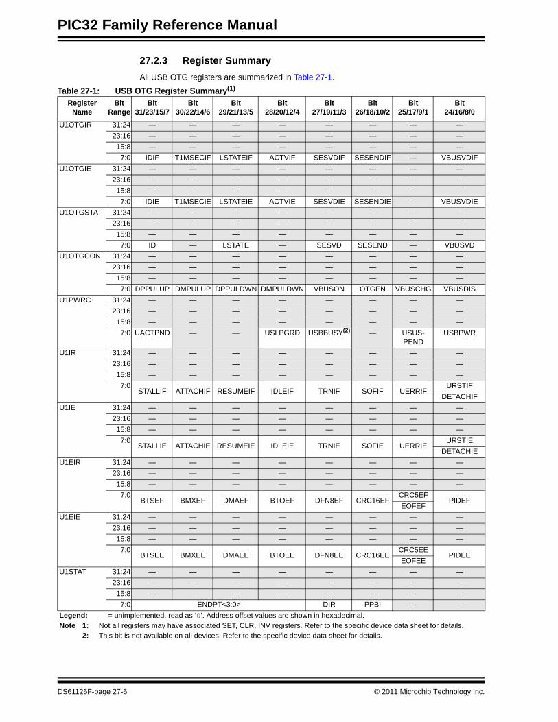
27.2.3 Register SummaryAll USB OTG registers are summarized in Table 27-1.
Table 27-1: USB OTG Register Summary(1)
RegisterName
Bit Range
Bit31/23/15/7
Bit30/22/14/6
Bit29/21/13/5
Bit28/20/12/4
Bit27/19/11/3
Bit26/18/10/2
Bit25/17/9/1
Bit24/16/8/0
U1OTGIR 31:24 — — — — — — — —23:16 — — — — — — — —
15:8 — — — — — — — —7:0 IDIF T1MSECIF LSTATEIF ACTVIF SESVDIF SESENDIF — VBUSVDIF
U1OTGIE 31:24 — — — — — — — —23:16 — — — — — — — —
15:8 — — — — — — — —7:0 IDIE T1MSECIE LSTATEIE ACTVIE SESVDIE SESENDIE — VBUSVDIE
U1OTGSTAT 31:24 — — — — — — — —23:16 — — — — — — — —
15:8 — — — — — — — —7:0 ID — LSTATE — SESVD SESEND — VBUSVD
U1OTGCON 31:24 — — — — — — — —23:16 — — — — — — — —
15:8 — — — — — — — —7:0 DPPULUP DMPULUP DPPULDWN DMPULDWN VBUSON OTGEN VBUSCHG VBUSDIS
U1PWRC 31:24 — — — — — — — —23:16 — — — — — — — —
15:8 — — — — — — — —7:0 UACTPND — — USLPGRD USBBUSY(2) — USUS-
PENDUSBPWR
U1IR 31:24 — — — — — — — —23:16 — — — — — — — —
15:8 — — — — — — — —7:0
STALLIF ATTACHIF RESUMEIF IDLEIF TRNIF SOFIF UERRIFURSTIF
DETACHIFU1IE 31:24 — — — — — — — —
23:16 — — — — — — — —15:8 — — — — — — — —
7:0STALLIE ATTACHIE RESUMEIE IDLEIE TRNIE SOFIE UERRIE
URSTIEDETACHIE
U1EIR 31:24 — — — — — — — —23:16 — — — — — — — —
15:8 — — — — — — — —7:0
BTSEF BMXEF DMAEF BTOEF DFN8EF CRC16EFCRC5EF
PIDEFEOFEF
U1EIE 31:24 — — — — — — — —23:16 — — — — — — — —
15:8 — — — — — — — —7:0
BTSEE BMXEE DMAEE BTOEE DFN8EE CRC16EECRC5EE
PIDEEEOFEE
U1STAT 31:24 — — — — — — — —23:16 — — — — — — — —
15:8 — — — — — — — —7:0 ENDPT<3:0> DIR PPBI — —
Legend: — = unimplemented, read as ‘0’. Address offset values are shown in hexadecimal.Note 1: Not all registers may have associated SET, CLR, INV registers. Refer to the specific device data sheet for details.
2: This bit is not available on all devices. Refer to the specific device data sheet for details.
DS61126F-page 27-6 © 2011 Microchip Technology Inc.
Section 27. USB On-The-Go (OTG)U
SB O
n-The-Go
(OTG
)
27
U1CON 31:24 — — — — — — — —23:16 — — — — — — — —
15:8 — — — — — — — —7:0
JSTATE SE0PKTDIS
USBRST HOSTEN RESUME PPBRSTUSBEN
TOKBUSY SOFENU1ADDR 31:24 — — — — — — — —
23:16 — — — — — — — —15:8 — — — — — — — —
7:0 LSPDEN DEVADDR<6:0>U1BDTP1 31:24 — — — — — — — —
23:16 — — — — — — — —15:8 — — — — — — — —
7:0 BDTPTRL<15:9> —U1FRML 31:24 — — — — — — — —
23:16 — — — — — — — —15:8 — — — — — — — —
7:0 FRML<7:0>U1FRMH 31:24 — — — — — — — —
23:16 — — — — — — — —15:8 — — — — — — — —
7:0 — — — — — FRMH<2:0>U1TOK 31:24 — — — — — — — —
23:16 — — — — — — — —15:8 — — — — — — — —
7:0 PID<3:0> EP<3:0>U1SOF 31:24 — — — — — — — —
23:16 — — — — — — — —15:8 — — — — — — — —
7:0 CNT<7:0>U1BDTP2 31:24 — — — — — — — —
23:16 — — — — — — — —15:8 — — — — — — — —
7:0 BDTPTRH<23:16>U1BDTP3 31:24 — — — — — — — —
23:16 — — — — — — — —15:8 — — — — — — — —
7:0 BDTPTRU<31:24>U1CNFG1 31:24 — — — — — — — —
23:16 — — — — — — — —15:8 — — — — — — — —
7:0 UTEYE UOEMON USBFRZ USBSIDL — — — UASUSPND(2)
U1EP0 31:24 — — — — — — — —23:16 — — — — — — — —
15:8 — — — — — — — —7:0 LSPD RETRYDIS — EPCONDIS EPRXEN EPTXEN EPSTALL EPHSHK
U1EP1 31:24 — — — — — — — —23:16 — — — — — — — —
15:8 — — — — — — — —7:0 — — — EPCONDIS EPRXEN EPTXEN EPSTALL EPHSHK
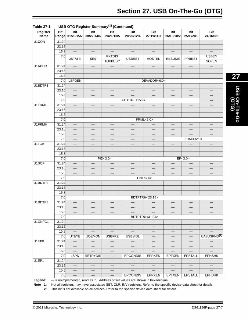
Table 27-1: USB OTG Register Summary(1) (Continued)Register
NameBit
RangeBit
31/23/15/7Bit
30/22/14/6Bit
29/21/13/5Bit
28/20/12/4Bit
27/19/11/3Bit
26/18/10/2Bit
25/17/9/1Bit
24/16/8/0
Legend: — = unimplemented, read as ‘0’. Address offset values are shown in hexadecimal.Note 1: Not all registers may have associated SET, CLR, INV registers. Refer to the specific device data sheet for details.
2: This bit is not available on all devices. Refer to the specific device data sheet for details.
© 2011 Microchip Technology Inc. DS61126F-page 27-7

PIC32 Family Reference Manual
U1EP2 31:24 — — — — — — — —23:16 — — — — — — — —
15:8 — — — — — — — —7:0 — — — EPCONDIS EPRXEN EPTXEN EPSTALL EPHSHK
U1EP3 31:24 — — — — — — — —23:16 — — — — — — — —
15:8 — — — — — — — —7:0 — — — EPCONDIS EPRXEN EPTXEN EPSTALL EPHSHK
U1EP4 31:24 — — — — — — — —23:16 — — — — — — — —
15:8 — — — — — — — —7:0 — — — EPCONDIS EPRXEN EPTXEN EPSTALL EPHSHK
U1EP5 31:24 — — — — — — — —23:16 — — — — — — — —
15:8 — — — — — — — —7:0 — — — EPCONDIS EPRXEN EPTXEN EPSTALL EPHSHK
U1EP6 31:24 — — — — — — — —23:16 — — — — — — — —
15:8 — — — — — — — —7:0 — — — EPCONDIS EPRXEN EPTXEN EPSTALL EPHSHK
U1EP7 31:24 — — — — — — — —23:16 — — — — — — — —
15:8 — — — — — — — —7:0 — — — EPCONDIS EPRXEN EPTXEN EPSTALL EPHSHK
U1EP8 31:24 — — — — — — — —23:16 — — — — — — — —
15:8 — — — — — — — —7:0 — — — EPCONDIS EPRXEN EPTXEN EPSTALL EPHSHK
U1EP9 31:24 — — — — — — — —23:16 — — — — — — — —
15:8 — — — — — — — —7:0 — — — EPCONDIS EPRXEN EPTXEN EPSTALL EPHSHK
U1EP10 31:24 — — — — — — — —23:16 — — — — — — — —
15:8 — — — — — — — —7:0 — — — EPCONDIS EPRXEN EPTXEN EPSTALL EPHSHK
U1EP11 31:24 — — — — — — — —23:16 — — — — — — — —
15:8 — — — — — — — —7:0 — — — EPCONDIS EPRXEN EPTXEN EPSTALL EPHSHK
U1EP12 31:24 — — — — — — — —23:16 — — — — — — — —
15:8 — — — — — — — —7:0 — — — EPCONDIS EPRXEN EPTXEN EPSTALL EPHSHK
U1EP13 31:24 — — — — — — — —23:16 — — — — — — — —
15:8 — — — — — — — —7:0 — — — EPCONDIS EPRXEN EPTXEN EPSTALL EPHSHK
Table 27-1: USB OTG Register Summary(1) (Continued)Register
NameBit
RangeBit
31/23/15/7Bit
30/22/14/6Bit
29/21/13/5Bit
28/20/12/4Bit
27/19/11/3Bit
26/18/10/2Bit
25/17/9/1Bit
24/16/8/0
Legend: — = unimplemented, read as ‘0’. Address offset values are shown in hexadecimal.Note 1: Not all registers may have associated SET, CLR, INV registers. Refer to the specific device data sheet for details.
2: This bit is not available on all devices. Refer to the specific device data sheet for details.
DS61126F-page 27-8 © 2011 Microchip Technology Inc.

Section 27. USB On-The-Go (OTG)U
SB O
n-The-Go
(OTG
)
27
U1EP14 31:24 — — — — — — — —23:16 — — — — — — — —
15:8 — — — — — — — —7:0 — — — EPCONDIS EPRXEN EPTXEN EPSTALL EPHSHK
U1EP15 31:24 — — — — — — — —23:16 — — — — — — — —
15:8 — — — — — — — —7:0 — — — EPCONDIS EPRXEN EPTXEN EPSTALL EPHSHK
Table 27-1: USB OTG Register Summary(1) (Continued)Register
NameBit
RangeBit
31/23/15/7Bit
30/22/14/6Bit
29/21/13/5Bit
28/20/12/4Bit
27/19/11/3Bit
26/18/10/2Bit
25/17/9/1Bit
24/16/8/0
Legend: — = unimplemented, read as ‘0’. Address offset values are shown in hexadecimal.Note 1: Not all registers may have associated SET, CLR, INV registers. Refer to the specific device data sheet for details.
2: This bit is not available on all devices. Refer to the specific device data sheet for details.
© 2011 Microchip Technology Inc. DS61126F-page 27-9

PIC32 Family Reference Manual
27.2.4 Register DefinitionsThis section provides a detailed description of each USB OTG register.
Register 27-1: U1OTGIR: USB OTG Interrupt Status RegisterU-0 U-0 U-0 U-0 U-0 U-0 U-0 U-0— — — — — — — —
bit 31 bit 24
U-0 U-0 U-0 U-0 U-0 U-0 U-0 U-0— — — — — — — —
bit 23 bit 16
U-0 U-0 U-0 U-0 U-0 U-0 U-0 U-0— — — — — — — —
bit 15 bit 8
R/K-0 R/K-0 R/K-0 R/K-0 R/K-0 R/K-0 U-0 R/K-0IDIF T1MSECIF LSTATEIF ACTVIF SESVDIF SESENDIF — VBUSVDIF
bit 7 bit 0
Legend:R = Readable bit W = Writable bit P = Programmable bit r = Reserved bitU = Unimplemented bit K = Write ‘1’ to clear -n = Bit Value at POR: (‘0’, ‘1’, x = unknown)
bit 31-8 Unimplemented: Read as ‘0’bit 7 IDIF: ID State Change Indicator bit
Write a ‘1’ to this bit to clear the interrupt.1 = Change in ID state detected0 = No change in ID state detected
bit 6 T1MSECIF: 1 Millisecond Timer bit Write a ‘1’ to this bit to clear the interrupt.1 = 1 millisecond timer has expired0 = 1 millisecond timer has not expired
bit 5 LSTATEIF: Line State Stable Indicator bitWrite a ‘1’ to this bit to clear the interrupt.1 = USB line state has been stable for 1 ms, but different from last time0 = USB line state has not been stable for 1 ms
bit 4 ACTVIF: Bus Activity Indicator bitWrite a ‘1’ to this bit to clear the interrupt. 1 = Activity on the D+, D-, ID or VBUS pins has caused the device to wake-up0 = Activity has not been detected
bit 3 SESVDIF: Session Valid Change Indicator bit Write a ‘1’ to this bit to clear the interrupt. 1 = VBUS voltage has dropped below the session end level0 = VBUS voltage has not dropped below the session end level
bit 2 SESENDIF: B-Device VBUS Change Indicator bitWrite a ‘1’ to this bit to clear the interrupt. 1 = A change on the session end input was detected0 = No change on the session end input was detected
bit 1 Unimplemented: Read as ‘0’bit 0 VBUSVDIF: A-Device VBUS Change Indicator bit
Write a ‘1’ to this bit to clear the interrupt. 1 = Change on the session valid input detected0 = No change on the session valid input detected
DS61126F-page 27-10 © 2011 Microchip Technology Inc.

Section 27. USB On-The-Go (OTG)U
SB O
n-The-Go
(OTG
)
27
Register 27-2: U1OTGIE: USB OTG Interrupt Enable RegisterU-0 U-0 U-0 U-0 U-0 U-0 U-0 U-0
— — — — — — — —
bit 31 bit 24
U-0 U-0 U-0 U-0 U-0 U-0 U-0 U-0
— — — — — — — —
bit 23 bit 16
U-0 U-0 U-0 U-0 U-0 U-0 U-0 U-0
— — — — — — — —
bit 15 bit 8
R/W-0 R/W-0 R/W-0 R/W-0 R/W-0 R/W-0 U-0 R/W-0
IDIE T1MSECIE LSTATEIE ACTVIE SESVDIE SESENDIE — VBUSVDIE
bit 7 bit 0
Legend:R = Readable bit W = Writable bit P = Programmable bit r = Reserved bit
U = Unimplemented bit -n = Bit Value at POR: (‘0’, ‘1’, x = Unknown)
bit 31-8 Unimplemented: Read as ‘0’
bit 7 IDIE: ID Interrupt Enable bit1 = ID interrupt enabled0 = ID interrupt disabled
bit 6 T1MSECIE: 1 Millisecond Timer Interrupt Enable bit1 = 1 millisecond timer interrupt enabled0 = 1 millisecond timer interrupt disabled
bit 5 LSTATEIE: Line State Interrupt Enable bit1 = Line state interrupt enabled0 = Line state interrupt disabled
bit 4 ACTVIE: Bus Activity Interrupt Enable bit1 = ACTIVITY interrupt enabled0 = ACTIVITY interrupt disabled
bit 3 SESVDIE: Session Valid Interrupt Enable bit1 = Session valid interrupt enabled0 = Session valid interrupt disabled
bit 2 SESENDIE: B-Session End Interrupt Enable bit1 = B-session end interrupt enabled0 = B-session end interrupt disabled
bit 1 Unimplemented: Read as ‘0’
bit 0 VBUSVDIE: A-VBUS Valid Interrupt Enable bit1 = A-VBUS valid interrupt enabled0 = A-VBUS valid interrupt disabled
© 2011 Microchip Technology Inc. DS61126F-page 27-11
PIC32 Family Reference Manual
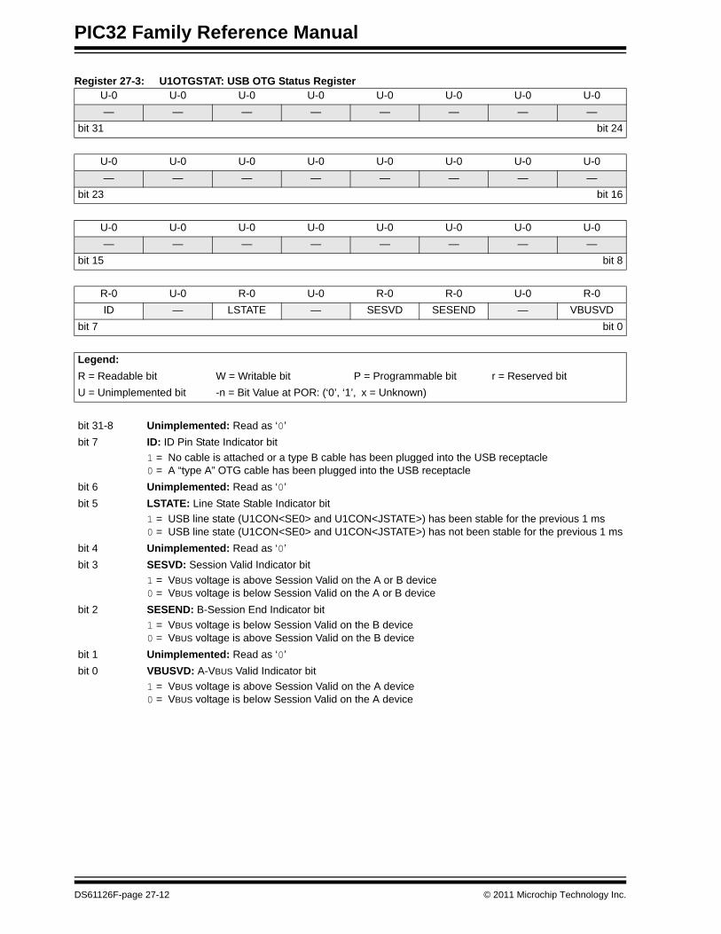
Register 27-3: U1OTGSTAT: USB OTG Status RegisterU-0 U-0 U-0 U-0 U-0 U-0 U-0 U-0— — — — — — — —
bit 31 bit 24
U-0 U-0 U-0 U-0 U-0 U-0 U-0 U-0— — — — — — — —
bit 23 bit 16
U-0 U-0 U-0 U-0 U-0 U-0 U-0 U-0— — — — — — — —
bit 15 bit 8
R-0 U-0 R-0 U-0 R-0 R-0 U-0 R-0ID — LSTATE — SESVD SESEND — VBUSVD
bit 7 bit 0
Legend:R = Readable bit W = Writable bit P = Programmable bit r = Reserved bitU = Unimplemented bit -n = Bit Value at POR: (‘0’, ‘1’, x = Unknown)
bit 31-8 Unimplemented: Read as ‘0’bit 7 ID: ID Pin State Indicator bit
1 = No cable is attached or a type B cable has been plugged into the USB receptacle0 = A “type A” OTG cable has been plugged into the USB receptacle
bit 6 Unimplemented: Read as ‘0’bit 5 LSTATE: Line State Stable Indicator bit
1 = USB line state (U1CON<SE0> and U1CON<JSTATE>) has been stable for the previous 1 ms0 = USB line state (U1CON<SE0> and U1CON<JSTATE>) has not been stable for the previous 1 ms
bit 4 Unimplemented: Read as ‘0’bit 3 SESVD: Session Valid Indicator bit
1 = VBUS voltage is above Session Valid on the A or B device0 = VBUS voltage is below Session Valid on the A or B device
bit 2 SESEND: B-Session End Indicator bit1 = VBUS voltage is below Session Valid on the B device0 = VBUS voltage is above Session Valid on the B device
bit 1 Unimplemented: Read as ‘0’bit 0 VBUSVD: A-VBUS Valid Indicator bit
1 = VBUS voltage is above Session Valid on the A device0 = VBUS voltage is below Session Valid on the A device
DS61126F-page 27-12 © 2011 Microchip Technology Inc.

Section 27. USB On-The-Go (OTG)U
SB O
n-The-Go
(OTG
)
27
Register 27-4: U1OTGCON: USB OTG Control RegisterU-0 U-0 U-0 U-0 U-0 U-0 U-0 U-0
— — — — — — — —
bit 31 bit 24
U-0 U-0 U-0 U-0 U-0 U-0 U-0 U-0
— — — — — — — —
bit 23 bit 16
U-0 U-0 U-0 U-0 U-0 U-0 U-0 U-0
— — — — — — — —
bit 15 bit 8
R/W-0 R/W-0 R/W-0 R/W-0 R/W-0 R/W-0 R/W-0 R/W-0
DPPULUP DMPULUP DPPULDWN DMPULDWN VBUSON OTGEN VBUSCHG VBUSDIS
bit 7 bit 0
Legend:R = Readable bit W = Writable bit P = Programmable bit r = Reserved bit
U = Unimplemented bit -n = Bit Value at POR: (‘0’, ‘1’, x = Unknown)
bit 31-8 Unimplemented: Read as ‘0’
bit 7 DPPULUP: D+ Pull-Up Enable bit1 = D+ data line pull-up resistor is enabled0 = D+ data line pull-up resistor is disabled
bit 6 DMPULUP: D- Pull-Up Enable bit1 = D- data line pull-up resistor is enabled0 = D- data line pull-up resistor is disabled
bit 5 DPPULDWN: D+ Pull-Down Enable bit1 = D+ data line pull-down resistor is enabled0 = D+ data line pull-down resistor is disabled
bit 4 DMPULDWN: D- Pull-Down Enable bit1 = D- data line pull-down resistor is enabled0 = D- data line pull-down resistor is disabled
bit 3 VBUSON: VBUS Power-on bit1 = VBUS line is powered0 = VBUS line is not powered
bit 2 OTGEN: OTG Functionality Enable bit1 = DPPULUP, DMPULUP, DPPULDWN and DMPULDWN bits are under software control0 = DPPULUP, DMPULUP, DPPULDWN and DMPULDWN bits are under USB hardware control
bit 1 VBUSCHG: VBUS Charge Enable bit1 = VBUS line is charged through a pull-up resistor0 = VBUS line is not charged through a resistor
bit 0 VBUSDIS: VBUS Discharge Enable bit1 = VBUS line is discharged through a pull-down resistor0 = VBUS line is not discharged through a resistor
© 2011 Microchip Technology Inc. DS61126F-page 27-13

PIC32 Family Reference Manual
Register 27-5: U1PWRC: USB Power Control RegisterU-0 U-0 U-0 U-0 U-0 U-0 U-0 U-0— — — — — — — —
bit 31 bit 24
U-0 U-0 U-0 U-0 U-0 U-0 U-0 U-0— — — — — — — —
bit 23 bit 16
U-0 U-0 U-0 U-0 U-0 U-0 U-0 U-0— — — — — — — —
bit 15 bit 8
HS, HC-x U-0 U-0 R/W-0 R/W-0 U-0 R/W-0 R/W-0UACTPND — — USLPGRD USBBUSY(1) — USUSPEND USBPWR
bit 7 bit 0
Legend:HC = Cleared by hardware HS = Set by hardwareR = Readable bit W = Writable bit P = Programmable bit r = Reserved bitU = Unimplemented bit -n = Bit Value at POR: (‘0’, ‘1’, x = Unknown)
bit 31-8 Unimplemented: Read as ‘0’bit 7 UACTPND: USB Activity Pending bit
1 = USB bus activity has been detected; but an interrupt is pending, it has not been generated yet0 = An interrupt is not pending
bit 6-5 Unimplemented: Read as ‘0’bit 4 USLPGRD: USB Sleep Entry Guard bit
1 = Sleep entry is blocked if USB bus activity is detected or if a notification is pending0 = USB OTG module does not block Sleep entry
bit 3 USBBUSY: USB OTG module Busy bit(1)
1 = USB OTG module is active or disabled, but not ready to be enabled0 = USB OTG module is not active and is ready to be enabledNote : When USBPWR = 0 and USBBUSY = 1, status from all other registers is invalid and writes
to all USB OTG module registers produce undefined results.bit 2 Unimplemented: Read as ‘0’bit 1 USUSPEND: USB Suspend Mode bit
1 = USB OTG module is placed in Suspend mode(The 48 MHz USB clock will be gated off. The transceiver is placed in a low-power state.)
0 = USB OTG module operates normallybit 0 USBPWR: USB Operation Enable bit
1 = USB OTG module is turned on0 = USB OTG module is disabled
(Outputs held inactive, device pins not used by USB, analog features are shut down to reducepower consumption.)
Note 1: This bit is not available on all devices. Refer to the specific device data sheet for details.
DS61126F-page 27-14 © 2011 Microchip Technology Inc.
Section 27. USB On-The-Go (OTG)U
SB O
n-The-Go
(OTG
)
27
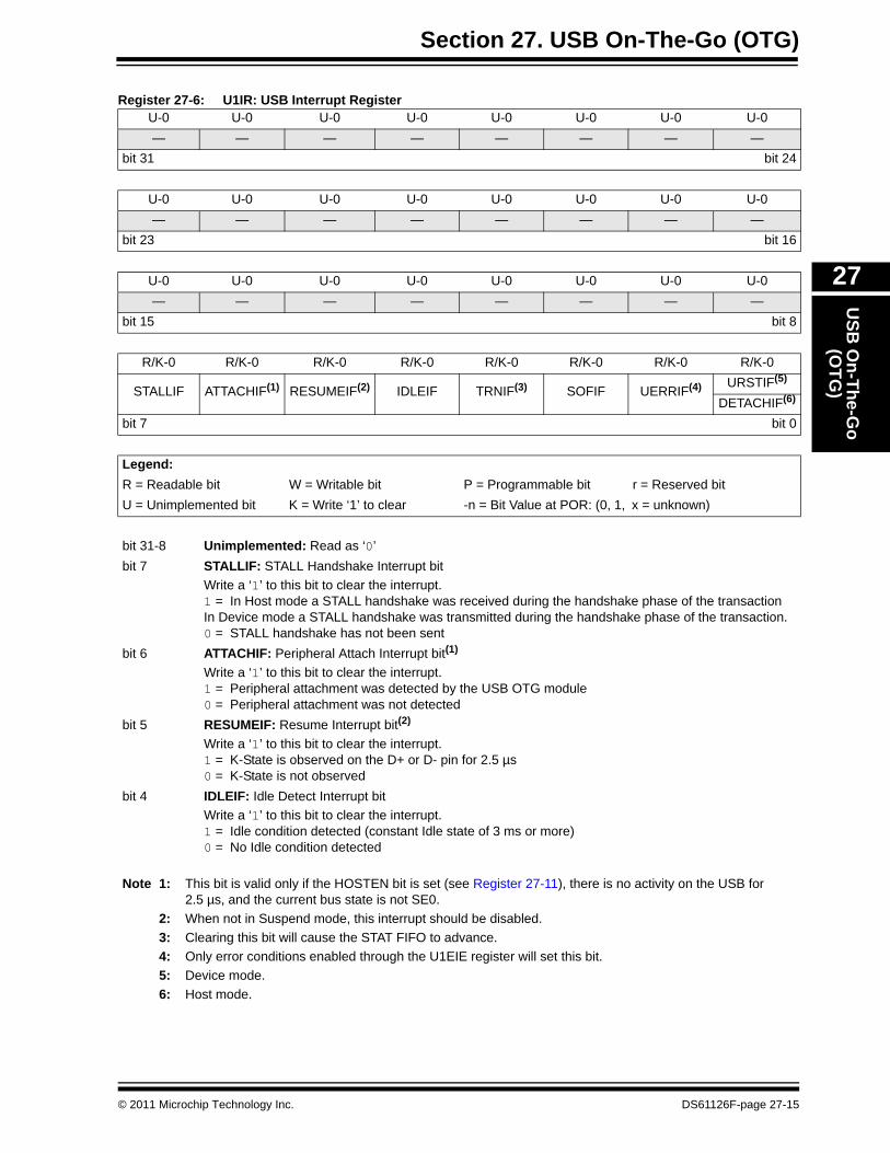
Register 27-6: U1IR: USB Interrupt RegisterU-0 U-0 U-0 U-0 U-0 U-0 U-0 U-0— — — — — — — —
bit 31 bit 24
U-0 U-0 U-0 U-0 U-0 U-0 U-0 U-0— — — — — — — —
bit 23 bit 16
U-0 U-0 U-0 U-0 U-0 U-0 U-0 U-0— — — — — — — —
bit 15 bit 8
R/K-0 R/K-0 R/K-0 R/K-0 R/K-0 R/K-0 R/K-0 R/K-0
STALLIF ATTACHIF(1) RESUMEIF(2) IDLEIF TRNIF(3) SOFIF UERRIF(4) URSTIF(5)
DETACHIF(6)
bit 7 bit 0
Legend:R = Readable bit W = Writable bit P = Programmable bit r = Reserved bitU = Unimplemented bit K = Write ‘1’ to clear -n = Bit Value at POR: (0, 1, x = unknown)
bit 31-8 Unimplemented: Read as ‘0’bit 7 STALLIF: STALL Handshake Interrupt bit
Write a ‘1’ to this bit to clear the interrupt. 1 = In Host mode a STALL handshake was received during the handshake phase of the transactionIn Device mode a STALL handshake was transmitted during the handshake phase of the transaction.0 = STALL handshake has not been sent
bit 6 ATTACHIF: Peripheral Attach Interrupt bit(1)
Write a ‘1’ to this bit to clear the interrupt. 1 = Peripheral attachment was detected by the USB OTG module0 = Peripheral attachment was not detected
bit 5 RESUMEIF: Resume Interrupt bit(2)
Write a ‘1’ to this bit to clear the interrupt. 1 = K-State is observed on the D+ or D- pin for 2.5 µs0 = K-State is not observed
bit 4 IDLEIF: Idle Detect Interrupt bitWrite a ‘1’ to this bit to clear the interrupt. 1 = Idle condition detected (constant Idle state of 3 ms or more)0 = No Idle condition detected
Note 1: This bit is valid only if the HOSTEN bit is set (see Register 27-11), there is no activity on the USB for 2.5 µs, and the current bus state is not SE0.
2: When not in Suspend mode, this interrupt should be disabled.3: Clearing this bit will cause the STAT FIFO to advance.4: Only error conditions enabled through the U1EIE register will set this bit.5: Device mode.6: Host mode.
© 2011 Microchip Technology Inc. DS61126F-page 27-15

PIC32 Family Reference Manual
bit 3 TRNIF: Token Processing Complete Interrupt bit(3)
Write a ‘1’ to this bit to clear the interrupt. 1 = Processing of current token is complete; a read of the U1STAT register will provide endpoint
information0 = Processing of current token not complete
bit 2 SOFIF: SOF Token Interrupt bitWrite a ‘1’ to this bit to clear the interrupt. 1 = SOF token received by the peripheral or the SOF threshold reached by the host0 = SOF token was not received nor threshold reached
bit 1 UERRIF: USB Error Condition Interrupt bit(4)
Write a ‘1’ to this bit to clear the interrupt. 1 = Unmasked error condition has occurred0 = Unmasked error condition has not occurred
bit 0 URSTIF: USB Reset Interrupt bit (Device mode)(5)
1 = Valid USB Reset has occurred0 = No USB Reset has occurredDETACHIF: USB Detach Interrupt bit (Host mode)(6)
1 = Peripheral detachment was detected by the USB OTG module0 = Peripheral detachment was not detected
Register 27-6: U1IR: USB Interrupt Register (Continued)
Note 1: This bit is valid only if the HOSTEN bit is set (see Register 27-11), there is no activity on the USB for 2.5 µs, and the current bus state is not SE0.
2: When not in Suspend mode, this interrupt should be disabled.3: Clearing this bit will cause the STAT FIFO to advance.4: Only error conditions enabled through the U1EIE register will set this bit.5: Device mode.6: Host mode.
DS61126F-page 27-16 © 2011 Microchip Technology Inc.

Section 27. USB On-The-Go (OTG)U
SB O
n-The-Go
(OTG
)
27
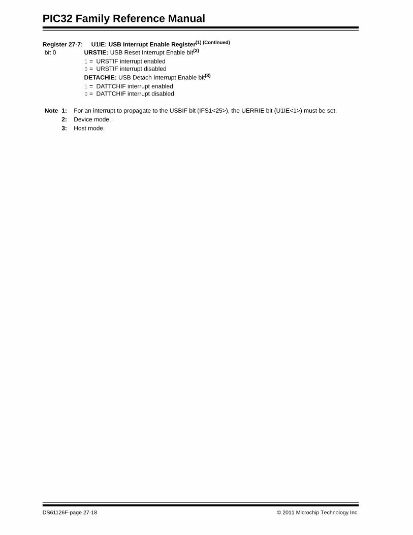
Register 27-7: U1IE: USB Interrupt Enable Register(1)
U-0 U-0 U-0 U-0 U-0 U-0 U-0 U-0— — — — — — — —
bit 31 bit 24
U-0 U-0 U-0 U-0 U-0 U-0 U-0 U-0— — — — — — — —
bit 23 bit 16
U-0 U-0 U-0 U-0 U-0 U-0 U-0 U-0— — — — — — — —
bit 15 bit 8
R/W-0 R/W-0 R/W-0 R/W-0 R/W-0 R/W-0 R/W-0 R/W-0
STALLIE ATTACHIE RESUMEIE IDLEIE TRNIE SOFIE UERRIEURSTIE(2)
DETACHIE(3)
bit 7 bit 0
Legend:R = Readable bit W = Writable bit P = Programmable bit r = Reserved bitU = Unimplemented bit -n = Bit Value at POR: (‘0’, ‘1’, x = Unknown)
bit 31-8 Unimplemented: Read as ‘0’bit 7 STALLIE: STALL Handshake Interrupt Enable bit
1 = STALL interrupt enabled0 = STALL interrupt disabled
bit 6 ATTACHIE: ATTACH Interrupt Enable bit1 = ATTACH interrupt enabled0 = ATTACH interrupt disabled
bit 5 RESUMEIE: RESUME Interrupt Enable bit1 = RESUME interrupt enabled0 = RESUME interrupt disabled
bit 4 IDLEIE: Idle Detect Interrupt Enable bit1 = Idle interrupt enabled0 = Idle interrupt disabled
bit 3 TRNIE: Token Processing Complete Interrupt Enable bit1 = TRNIF interrupt enabled0 = TRNIF interrupt disabled
bit 2 SOFIE: SOF Token Interrupt Enable bit1 = SOFIF interrupt enabled0 = SOFIF interrupt disabled
bit 1 UERRIE: USB Error Interrupt Enable bit1 = USB Error interrupt enabled0 = USB Error interrupt disabled
Note 1: For an interrupt to propagate to the USBIF bit (IFS1<25>), the UERRIE bit (U1IE<1>) must be set.2: Device mode.3: Host mode.
© 2011 Microchip Technology Inc. DS61126F-page 27-17
PIC32 Family Reference Manual
bit 0 URSTIE: USB Reset Interrupt Enable bit(2)
1 = URSTIF interrupt enabled0 = URSTIF interrupt disabledDETACHIE: USB Detach Interrupt Enable bit(3)
1 = DATTCHIF interrupt enabled0 = DATTCHIF interrupt disabled
Register 27-7: U1IE: USB Interrupt Enable Register(1) (Continued)
Note 1: For an interrupt to propagate to the USBIF bit (IFS1<25>), the UERRIE bit (U1IE<1>) must be set.2: Device mode.3: Host mode.
DS61126F-page 27-18 © 2011 Microchip Technology Inc.
Section 27. USB On-The-Go (OTG)U
SB O
n-The-Go
(OTG
)
27
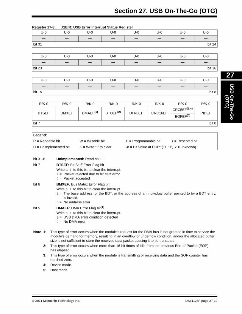
Register 27-8: U1EIR: USB Error Interrupt Status RegisterU-0 U-0 U-0 U-0 U-0 U-0 U-0 U-0
— — — — — — — —
bit 31 bit 24
U-0 U-0 U-0 U-0 U-0 U-0 U-0 U-0
— — — — — — — —
bit 23 bit 16
U-0 U-0 U-0 U-0 U-0 U-0 U-0 U-0
— — — — — — — —
bit 15 bit 8
R/K-0 R/K-0 R/K-0 R/K-0 R/K-0 R/K-0 R/K-0 R/K-0
BTSEF BMXEF DMAEF(1) BTOEF(2) DFN8EF CRC16EFCRC5EF(3,4)
PIDEFEOFEF(5)
bit 7 bit 0
Legend:R = Readable bit W = Writable bit P = Programmable bit r = Reserved bit
U = Unimplemented bit K = Write ‘1’ to clear -n = Bit Value at POR: (‘0’, ‘1’, x = unknown)
bit 31-8 Unimplemented: Read as ‘0’
bit 7 BTSEF: Bit Stuff Error Flag bitWrite a ‘1’ to this bit to clear the interrupt. 1 = Packet rejected due to bit stuff error0 = Packet accepted
bit 6 BMXEF: Bus Matrix Error Flag bitWrite a ‘1’ to this bit to clear the interrupt. 1 = The base address, of the BDT, or the address of an individual buffer pointed to by a BDT entry,
is invalid. 0 = No address error
bit 5 DMAEF: DMA Error Flag bit(1)
Write a ‘1’ to this bit to clear the interrupt. 1 = USB DMA error condition detected0 = No DMA error
Note 1: This type of error occurs when the module’s request for the DMA bus is not granted in time to service the module’s demand for memory, resulting in an overflow or underflow condition, and/or the allocated buffer size is not sufficient to store the received data packet causing it to be truncated.
2: This type of error occurs when more than 16-bit-times of Idle from the previous End-of-Packet (EOP) has elapsed.
3: This type of error occurs when the module is transmitting or receiving data and the SOF counter has reached zero.
4: Device mode.5: Host mode.
© 2011 Microchip Technology Inc. DS61126F-page 27-19

PIC32 Family Reference Manual
bit 4 BTOEF: Bus Turnaround Time-Out Error Flag bit(2)
Write a ‘1’ to this bit to clear the interrupt. 1 = Bus turnaround time-out has occurred0 = No bus turnaround time-out
bit 3 DFN8EF: Data Field Size Error Flag bitWrite a ‘1’ to this bit to clear the interrupt. 1 = Data field received is not an integral number of bytes0 = Data field received is an integral number of bytes
bit 2 CRC16EF: CRC16 Failure Flag bitWrite a ‘1’ to this bit to clear the interrupt. 1 = Data packet rejected due to CRC16 error0 = Data packet accepted
bit 1 CRC5EF: CRC5 Host Error Flag bit(3,4)
Write a ‘1’ to this bit to clear the interrupt. 1 = Token packet rejected due to CRC5 error0 = Token packet acceptedEOFEF: EOF Error Flag bit(5)
1 = EOF error condition detected0 = No EOF error condition
bit 0 PIDEF: PID Check Failure Flag bit1 = PID check failed0 = PID check passed
Register 27-8: U1EIR: USB Error Interrupt Status Register (Continued)
Note 1: This type of error occurs when the module’s request for the DMA bus is not granted in time to service the module’s demand for memory, resulting in an overflow or underflow condition, and/or the allocated buffer size is not sufficient to store the received data packet causing it to be truncated.
2: This type of error occurs when more than 16-bit-times of Idle from the previous End-of-Packet (EOP) has elapsed.
3: This type of error occurs when the module is transmitting or receiving data and the SOF counter has reached zero.
4: Device mode.5: Host mode.
DS61126F-page 27-20 © 2011 Microchip Technology Inc.

Section 27. USB On-The-Go (OTG)U
SB O
n-The-Go
(OTG
)
27
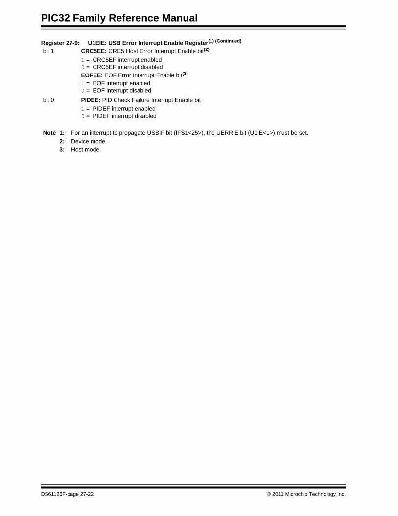
Register 27-9: U1EIE: USB Error Interrupt Enable Register(1)
U-0 U-0 U-0 U-0 U-0 U-0 U-0 U-0
— — — — — — — —
bit 31 bit 24
U-0 U-0 U-0 U-0 U-0 U-0 U-0 U-0
— — — — — — — —
bit 23 bit 16
U-0 U-0 U-0 U-0 U-0 U-0 U-0 U-0
— — — — — — — —
bit 15 bit 8
R/W-0 R/W-0 R/W-0 R/W-0 R/W-0 R/W-0 R/W-0 R/W-0
BTSEE BMXEE DMAEE BTOEE DFN8EE CRC16EECRC5EE(2)
PIDEEEOFEE(3)
bit 7 bit 0
Legend:R = Readable bit W = Writable bit P = Programmable bit r = Reserved bit
U = Unimplemented bit -n = Bit Value at POR: (‘0’, ‘1’, x = Unknown)
bit 31-8 Unimplemented: Read as ‘0’
bit 7 BTSEE: Bit Stuff Error Interrupt Enable bit1 = BTSEF interrupt enabled0 = BTSEF interrupt disabled
bit 6 BMXEE: Bus Matrix Error Interrupt Enable bit1 = BMXEF interrupt enabled0 = BMXEF interrupt disabled
bit 5 DMAEE: DMA Error Interrupt Enable bit1 = DMAEF interrupt enabled0 = DMAEF interrupt disabled
bit 4 BTOEE: Bus Turnaround Time-out Error Interrupt Enable bit1 = BTOEF interrupt enabled0 = BTOEF interrupt disabled
bit 3 DFN8EE: Data Field Size Error Interrupt Enable bit1 = DFN8EF interrupt enabled0 = DFN8EF interrupt disabled
bit 2 CRC16EE: CRC16 Failure Interrupt Enable bit1 = CRC16EF interrupt enabled0 = CRC16EF interrupt disabled
Note 1: For an interrupt to propagate USBIF bit (IFS1<25>), the UERRIE bit (U1IE<1>) must be set.2: Device mode.3: Host mode.
© 2011 Microchip Technology Inc. DS61126F-page 27-21
PIC32 Family Reference Manual
bit 1 CRC5EE: CRC5 Host Error Interrupt Enable bit(2)
1 = CRC5EF interrupt enabled0 = CRC5EF interrupt disabledEOFEE: EOF Error Interrupt Enable bit(3)
1 = EOF interrupt enabled0 = EOF interrupt disabled
bit 0 PIDEE: PID Check Failure Interrupt Enable bit1 = PIDEF interrupt enabled0 = PIDEF interrupt disabled
Register 27-9: U1EIE: USB Error Interrupt Enable Register(1) (Continued)
Note 1: For an interrupt to propagate USBIF bit (IFS1<25>), the UERRIE bit (U1IE<1>) must be set.2: Device mode.3: Host mode.
DS61126F-page 27-22 © 2011 Microchip Technology Inc.

Section 27. USB On-The-Go (OTG)U
SB O
n-The-Go
(OTG
)
27
Register 27-10: U1STAT: USB Status Register(1)
U-0 U-0 U-0 U-0 U-0 U-0 U-0 U-0— — — — — — — —
bit 31 bit 24
U-0 U-0 U-0 U-0 U-0 U-0 U-0 U-0— — — — — — — —
bit 23 bit 16
U-0 U-0 U-0 U-0 U-0 U-0 U-0 U-0— — — — — — — —
bit 15 bit 8
R-x R-x R-x R-x R-x R-x U-0 U-0ENDPT<3:0> DIR PPBI — —
bit 7 bit 0
Legend:R = Readable bit W = Writable bit P = Programmable bit r = Reserved bitU = Unimplemented bit -n = Bit Value at POR: (‘0’, ‘1’, x = Unknown)
bit 31-8 Unimplemented: Read as ‘0’bit 7-4 ENDPT<3:0>: Encoded Number of Last Endpoint Activity bits
(Represents the number of the BDT, updated by the last USB transfer.)1111 = Endpoint 151110 = Endpoint 14•••0001 = Endpoint 10000 = Endpoint 0
bit 3 DIR: Last BD Direction Indicator bit1 = Last transaction was a transmit transfer (TX)0 = Last transaction was a receive transfer (RX)
bit 2 PPBI: Ping-Pong BD Pointer Indicator bit1 = The last transaction was to the ODD BD bank0 = The last transaction was to the EVEN BD bank
bit 1-0 Unimplemented: Read as ‘0’
Note 1: The U1STAT register is a window into a 4 byte FIFO maintained by the USB OTG module. U1STAT value is only valid when the TRNIF bit (U1IR<3>) is active. Clearing the TRNIF bit (U1IR<3>) advances the FIFO. Data in register is invalid when the TRNIF bit (U1IR<3>) = 0.
© 2011 Microchip Technology Inc. DS61126F-page 27-23
PIC32 Family Reference Manual
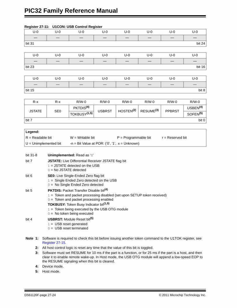
Register 27-11: U1CON: USB Control RegisterU-0 U-0 U-0 U-0 U-0 U-0 U-0 U-0
— — — — — — — —
bit 31 bit 24
U-0 U-0 U-0 U-0 U-0 U-0 U-0 U-0
— — — — — — — —
bit 23 bit 16
U-0 U-0 U-0 U-0 U-0 U-0 U-0 U-0
— — — — — — — —
bit 15 bit 8
R-x R-x R/W-0 R/W-0 R/W-0 R/W-0 R/W-0 R/W-0
JSTATE SE0PKTDIS(4)
USBRST HOSTEN(2) RESUME(3) PPBRSTUSBEN(4)
TOKBUSY(1,5) SOFEN(5)
bit 7 bit 0
Legend:R = Readable bit W = Writable bit P = Programmable bit r = Reserved bit
U = Unimplemented bit -n = Bit Value at POR: (‘0’, ‘1’, x = Unknown)
bit 31-8 Unimplemented: Read as ‘0’
bit 7 JSTATE: Live Differential Receiver JSTATE flag bit1 = JSTATE detected on the USB0 = No JSTATE detected
bit 6 SE0: Live Single-Ended Zero flag bit1 = Single Ended Zero detected on the USB0 = No Single Ended Zero detected
bit 5 PKTDIS: Packet Transfer Disable bit(4)
1 = Token and packet processing disabled (set upon SETUP token received)0 = Token and packet processing enabledTOKBUSY: Token Busy Indicator bit(1,5)
1 = Token being executed by the USB OTG module0 = No token being executed
bit 4 USBRST: Module Reset bit(5)
1 = USB reset generated0 = USB reset terminated
Note 1: Software is required to check this bit before issuing another token command to the U1TOK register, see Register 27-15.
2: All host control logic is reset any time that the value of this bit is toggled.3: Software must set RESUME for 10 ms if the part is a function, or for 25 ms if the part is a host, and then
clear it to enable remote wake-up. In Host mode, the USB OTG module will append a low-speed EOP to the RESUME signaling when this bit is cleared.
4: Device mode.5: Host mode.
DS61126F-page 27-24 © 2011 Microchip Technology Inc.

Section 27. USB On-The-Go (OTG)U
SB O
n-The-Go
(OTG
)
27
bit 3 HOSTEN: Host Mode Enable bit(2)
1 = USB host capability enabled0 = USB host capability disabled
bit 2 RESUME: RESUME Signaling Enable bit(3)
1 = RESUME signaling activated0 = RESUME signaling disabled
bit 1 PPBRST: Ping-Pong Buffers Reset bit1 = Reset all Even/Odd buffer pointers to the EVEN BD banks0 = Even/Odd buffer pointers not being Reset
bit 0 USBEN: USB OTG Module Enable bit(4)
1 = USB OTG module and supporting circuitry enabled0 = USB OTG module and supporting circuitry disabledSOFEN: SOF Enable bit(5)
1 = SOF token sent every 1 ms0 = SOF token disabled
Register 27-11: U1CON: USB Control Register (Continued)
Note 1: Software is required to check this bit before issuing another token command to the U1TOK register, see Register 27-15.
2: All host control logic is reset any time that the value of this bit is toggled.3: Software must set RESUME for 10 ms if the part is a function, or for 25 ms if the part is a host, and then
clear it to enable remote wake-up. In Host mode, the USB OTG module will append a low-speed EOP to the RESUME signaling when this bit is cleared.
4: Device mode.5: Host mode.
© 2011 Microchip Technology Inc. DS61126F-page 27-25

PIC32 Family Reference Manual
Register 27-12: U1ADDR: USB Address RegisterU-0 U-0 U-0 U-0 U-0 U-0 U-0 U-0
— — — — — — — —
bit 31 bit 24
U-0 U-0 U-0 U-0 U-0 U-0 U-0 U-0
— — — — — — — —
bit 23 bit 16
U-0 U-0 U-0 U-0 U-0 U-0 U-0 U-0
— — — — — — — —
bit 15 bit 8
R/W-0 R/W-0 R/W-0 R/W-0 R/W-0 R/W-0 R/W-0 R/W-0
LSPDEN DEVADDR<6:0>
bit 7 bit 0
Legend:R = Readable bit W = Writable bit P = Programmable bit r = Reserved bit
U = Unimplemented bit -n = Bit Value at POR: (‘0’, ‘1’, x = Unknown)
bit 31-8 Unimplemented: Read as ‘0’
bit 7 LSPDEN: Low-Speed Enable Indicator bit1 = Next token command to be executed at low-speed0 = Next token command to be executed at full-speed
bit 6-0 DEVADDR<6:0>: 7-bit USB Device Address bits
DS61126F-page 27-26 © 2011 Microchip Technology Inc.

Section 27. USB On-The-Go (OTG)U
SB O
n-The-Go
(OTG
)
27
Register 27-13: U1FRML: USB Frame Number Low RegisterU-0 U-0 U-0 U-0 U-0 U-0 U-0 U-0
— — — — — — — —
bit 31 bit 24
U-0 U-0 U-0 U-0 U-0 U-0 U-0 U-0
— — — — — — — —
bit 23 bit 16
U-0 U-0 U-0 U-0 U-0 U-0 U-0 U-0
— — — — — — — —
bit 15 bit 8
R-0 R-0 R-0 R-0 R-0 R-0 R-0 R-0
FRML<7:0>
bit 7 bit 0
Legend:R = Readable bit W = Writable bit P = Programmable bit r = Reserved bit
U = Unimplemented bit -n = Bit Value at POR: (‘0’, ‘1’, x = Unknown)
bit 31-8 Unimplemented: Read as ‘0’
bit 7-0 FRML<7:0>: The 11-bit Frame Number Lower bitsThe register bits are updated with the current frame number whenever a SOF TOKEN is received.
© 2011 Microchip Technology Inc. DS61126F-page 27-27
PIC32 Family Reference Manual
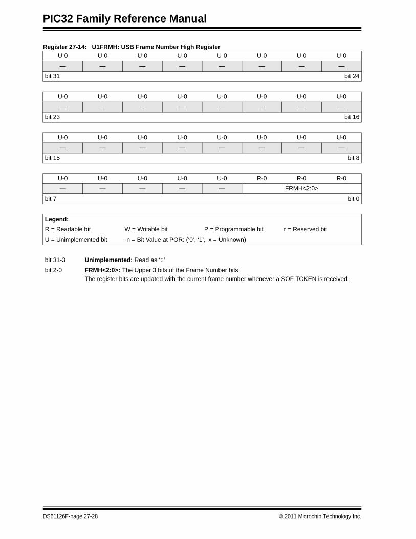
Register 27-14: U1FRMH: USB Frame Number High RegisterU-0 U-0 U-0 U-0 U-0 U-0 U-0 U-0
— — — — — — — —
bit 31 bit 24
U-0 U-0 U-0 U-0 U-0 U-0 U-0 U-0
— — — — — — — —
bit 23 bit 16
U-0 U-0 U-0 U-0 U-0 U-0 U-0 U-0
— — — — — — — —
bit 15 bit 8
U-0 U-0 U-0 U-0 U-0 R-0 R-0 R-0
— — — — — FRMH<2:0>
bit 7 bit 0
Legend:R = Readable bit W = Writable bit P = Programmable bit r = Reserved bit
U = Unimplemented bit -n = Bit Value at POR: (‘0’, ‘1’, x = Unknown)
bit 31-3 Unimplemented: Read as ‘0’
bit 2-0 FRMH<2:0>: The Upper 3 bits of the Frame Number bitsThe register bits are updated with the current frame number whenever a SOF TOKEN is received.
DS61126F-page 27-28 © 2011 Microchip Technology Inc.
Section 27. USB On-The-Go (OTG)U
SB O
n-The-Go
(OTG
)
27
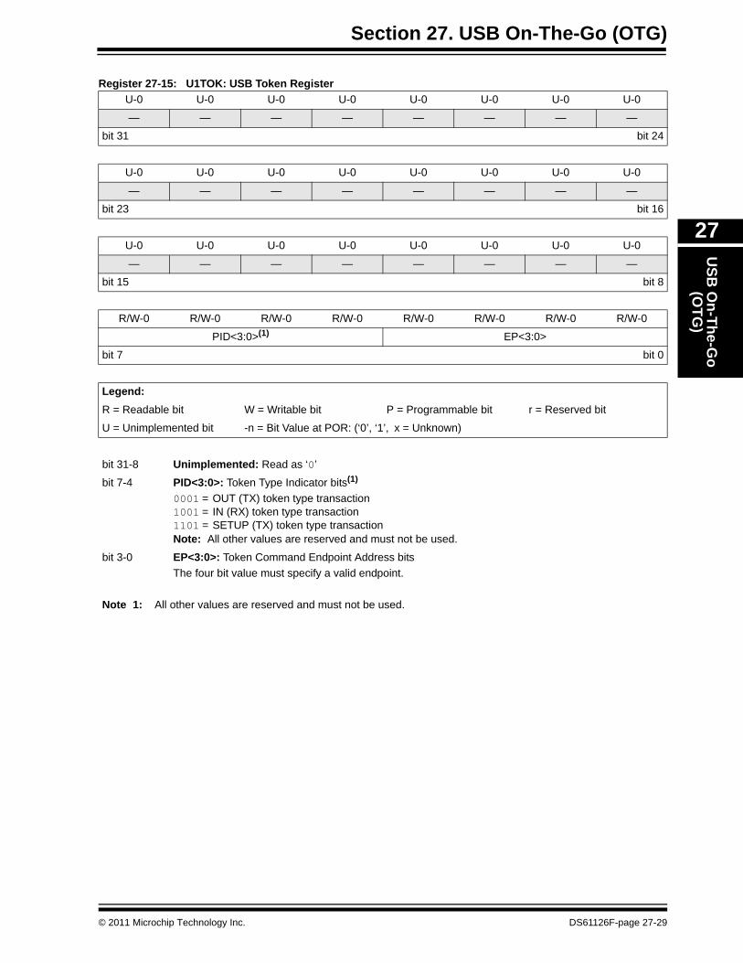
Register 27-15: U1TOK: USB Token RegisterU-0 U-0 U-0 U-0 U-0 U-0 U-0 U-0
— — — — — — — —
bit 31 bit 24
U-0 U-0 U-0 U-0 U-0 U-0 U-0 U-0
— — — — — — — —
bit 23 bit 16
U-0 U-0 U-0 U-0 U-0 U-0 U-0 U-0
— — — — — — — —
bit 15 bit 8
R/W-0 R/W-0 R/W-0 R/W-0 R/W-0 R/W-0 R/W-0 R/W-0
PID<3:0>(1) EP<3:0>
bit 7 bit 0
Legend:R = Readable bit W = Writable bit P = Programmable bit r = Reserved bit
U = Unimplemented bit -n = Bit Value at POR: (‘0’, ‘1’, x = Unknown)
bit 31-8 Unimplemented: Read as ‘0’
bit 7-4 PID<3:0>: Token Type Indicator bits(1) 0001 = OUT (TX) token type transaction1001 = IN (RX) token type transaction1101 = SETUP (TX) token type transactionNote: All other values are reserved and must not be used.
bit 3-0 EP<3:0>: Token Command Endpoint Address bits The four bit value must specify a valid endpoint.
Note 1: All other values are reserved and must not be used.
© 2011 Microchip Technology Inc. DS61126F-page 27-29

PIC32 Family Reference Manual
Register 27-16: U1SOF: USB SOF Threshold RegisterU-0 U-0 U-0 U-0 U-0 U-0 U-0 U-0
— — — — — — — —
bit 31 bit 24
U-0 U-0 U-0 U-0 U-0 U-0 U-0 U-0
— — — — — — — —
bit 23 bit 16
U-0 U-0 U-0 U-0 U-0 U-0 U-0 U-0
— — — — — — — —
bit 15 bit 8
R/W-0 R/W-0 R/W-0 R/W-0 R/W-0 R/W-0 R/W-0 R/W-0
CNT<7:0>
bit 7 bit 0
Legend:R = Readable bit W = Writable bit P = Programmable bit r = Reserved bit
U = Unimplemented bit -n = Bit Value at POR: (‘0’, ‘1’, x = Unknown)
bit 31-8 Unimplemented: Read as ‘0’
bit 7-0 CNT<7:0>: SOF Threshold Value bitsTypical values of the threshold are:0100 1010 = 64-byte packet0010 1010 = 32-byte packet0001 1010 = 16-byte packet0001 0010 = 8-byte packet
DS61126F-page 27-30 © 2011 Microchip Technology Inc.

Section 27. USB On-The-Go (OTG)U
SB O
n-The-Go
(OTG
)
27
Register 27-17: U1BDTP1: USB BDT RegisterU-0 U-0 U-0 U-0 U-0 U-0 U-0 U-0
— — — — — — — —
bit 31 bit 24
U-0 U-0 U-0 U-0 U-0 U-0 U-0 U-0
— — — — — — — —
bit 23 bit 16
U-0 U-0 U-0 U-0 U-0 U-0 U-0 U-0
— — — — — — — —
bit 15 bit 8
R/W-0 R/W-0 R/W-0 R/W-0 R/W-0 R/W-0 R/W-0 U-0
BDTPTRL<15:9> —
bit 7 bit 0
Legend:R = Readable bit W = Writable bit P = Programmable bit r = Reserved bit
U = Unimplemented bit -n = Bit Value at POR: (‘0’, ‘1’, x = Unknown)
bit 31-8 Unimplemented: Read as ‘0’
bit 7-1 BDTPTRL<15:9>: BDT Base Address Low bitsThis 7-bit value provides address bits 15 through 9 of the BDT base address, which defines the BDT’sstarting location in the system memory. The 32-bit BDT base address is 512 byte aligned.
bit 0 Unimplemented: Read as ‘0’
© 2011 Microchip Technology Inc. DS61126F-page 27-31
PIC32 Family Reference Manual
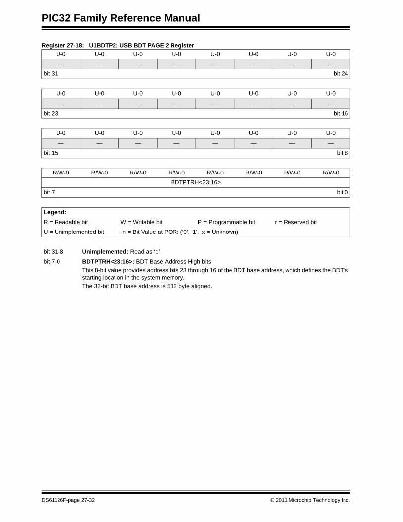
Register 27-18: U1BDTP2: USB BDT PAGE 2 RegisterU-0 U-0 U-0 U-0 U-0 U-0 U-0 U-0
— — — — — — — —
bit 31 bit 24
U-0 U-0 U-0 U-0 U-0 U-0 U-0 U-0
— — — — — — — —
bit 23 bit 16
U-0 U-0 U-0 U-0 U-0 U-0 U-0 U-0
— — — — — — — —
bit 15 bit 8
R/W-0 R/W-0 R/W-0 R/W-0 R/W-0 R/W-0 R/W-0 R/W-0
BDTPTRH<23:16>
bit 7 bit 0
Legend:R = Readable bit W = Writable bit P = Programmable bit r = Reserved bit
U = Unimplemented bit -n = Bit Value at POR: (‘0’, ‘1’, x = Unknown)
bit 31-8 Unimplemented: Read as ‘0’
bit 7-0 BDTPTRH<23:16>: BDT Base Address High bitsThis 8-bit value provides address bits 23 through 16 of the BDT base address, which defines the BDT’sstarting location in the system memory. The 32-bit BDT base address is 512 byte aligned.
DS61126F-page 27-32 © 2011 Microchip Technology Inc.

Section 27. USB On-The-Go (OTG)U
SB O
n-The-Go
(OTG
)
27
Register 27-19: U1BDTP3: USB BDT PAGE 3 RegisterU-0 U-0 U-0 U-0 U-0 U-0 U-0 U-0
— — — — — — — —
bit 31 bit 24
U-0 U-0 U-0 U-0 U-0 U-0 U-0 U-0
— — — — — — — —
bit 23 bit 16
U-0 U-0 U-0 U-0 U-0 U-0 U-0 U-0
— — — — — — — —
bit 15 bit 8
R/W-0 R/W-0 R/W-0 R/W-0 R/W-0 R/W-0 R/W-0 R/W-0
BDTPTRU<31:24>
bit 7 bit 0
Legend:R = Readable bit W = Writable bit P = Programmable bit r = Reserved bit
U = Unimplemented bit -n = Bit Value at POR: (‘0’, ‘1’, x = Unknown)
bit 31-8 Unimplemented: Read as ‘0’
bit 7-0 BDTPTRU<31:24>: BDT Base Address Upper bitsThis 8-bit value provides address bits 31 through 24 of the BDT base address, which defines the BDT’sstarting location in the system memory. The 32-bit BDT base address is 512 byte aligned.
© 2011 Microchip Technology Inc. DS61126F-page 27-33

PIC32 Family Reference Manual
Register 27-20: U1CNFG1: USB Configuration 1 RegisterU-0 U-0 U-0 U-0 U-0 U-0 U-0 U-0
— — — — — — — —
bit 31 bit 24
U-0 U-0 U-0 U-0 U-0 U-0 U-0 U-0
— — — — — — — —
bit 23 bit 16
U-0 U-0 U-0 U-0 U-0 U-0 U-0 U-0
— — — — — — — —
bit 15 bit 8
R/W-0 R/W-0 R/W-0 R/W-0 U-0 U-0 U-0 R/W-0
UTEYE UOEMON USBFRZ USBSIDL — — — UASUSPND(1)
bit 7 bit 0
Legend:R = Readable bit W = Writable bit P = Programmable bit r = Reserved bit
U = Unimplemented bit -n = Bit Value at POR: (‘0’, ‘1’, x = Unknown)
bit 31-8 Unimplemented: Read as ‘0’
bit 7 UTEYE: USB Eye-Pattern Test Enable bit1 = Eye-Pattern Test enabled0 = Eye-Pattern Test disabled
bit 6 UOEMON: USB OE Monitor Enable bit1 = OE signal active; it indicates intervals during which the D+/D- lines are driving0 = OE signal inactive
bit 5 USBFRZ: Freeze in Debug Mode bit1 = When emulator is in Debug mode, module freezes operation0 = When emulator is in Debug mode, module continues operation
bit 4 USBSIDL: Stop in Idle Mode bit1 = Discontinue module operation when device enters Idle mode0 = Continue module operation in Idle mode
bit 3-1 Unimplemented: Read as ‘0’
bit 0 UASUSPND: Automatic Suspend Enable bit(1)
1 = USB OTG module automatically suspends upon entry to Sleep mode. See the USUSPEND bit(U1PWRC<1>) in Register 27-5.
0 = USB OTG module does not automatically suspend upon entry to Sleep mode. Software must usethe USUSPEND bit (U1PWRC<1>) to suspend the module, including the USB 48 MHz clock
Note 1: This bit is not available on all devices. Refer to the specific device data sheet for details.
DS61126F-page 27-34 © 2011 Microchip Technology Inc.
Section 27. USB On-The-Go (OTG)U
SB O
n-The-Go
(OTG
)
27
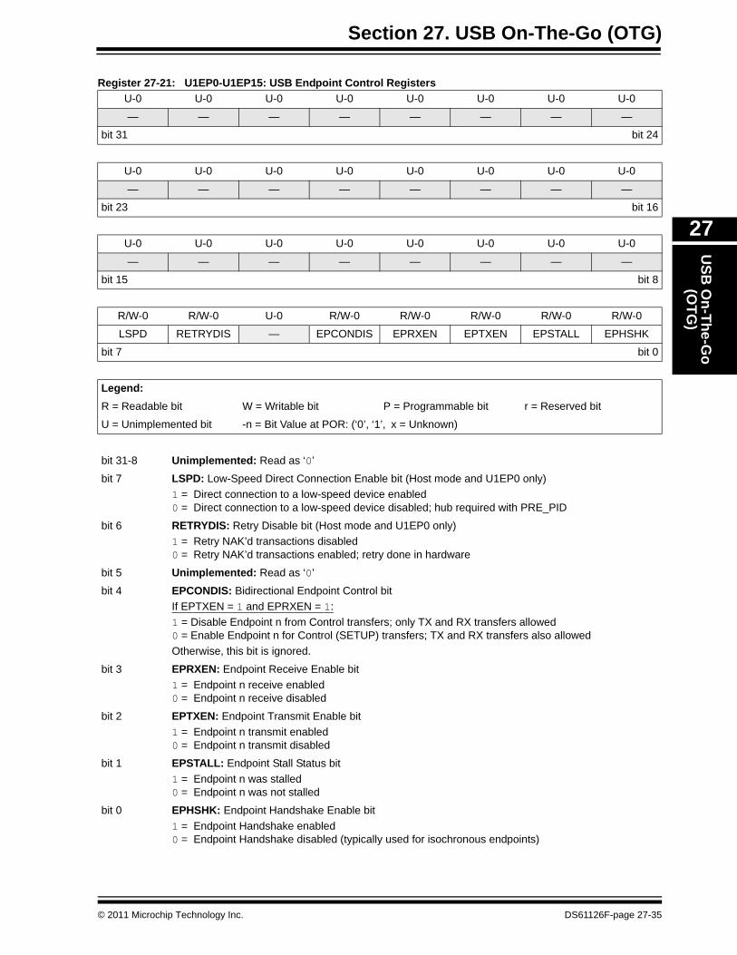
Register 27-21: U1EP0-U1EP15: USB Endpoint Control RegistersU-0 U-0 U-0 U-0 U-0 U-0 U-0 U-0
— — — — — — — —
bit 31 bit 24
U-0 U-0 U-0 U-0 U-0 U-0 U-0 U-0
— — — — — — — —
bit 23 bit 16
U-0 U-0 U-0 U-0 U-0 U-0 U-0 U-0
— — — — — — — —
bit 15 bit 8
R/W-0 R/W-0 U-0 R/W-0 R/W-0 R/W-0 R/W-0 R/W-0
LSPD RETRYDIS — EPCONDIS EPRXEN EPTXEN EPSTALL EPHSHK
bit 7 bit 0
Legend:R = Readable bit W = Writable bit P = Programmable bit r = Reserved bit
U = Unimplemented bit -n = Bit Value at POR: (‘0’, ‘1’, x = Unknown)
bit 31-8 Unimplemented: Read as ‘0’
bit 7 LSPD: Low-Speed Direct Connection Enable bit (Host mode and U1EP0 only)1 = Direct connection to a low-speed device enabled0 = Direct connection to a low-speed device disabled; hub required with PRE_PID
bit 6 RETRYDIS: Retry Disable bit (Host mode and U1EP0 only)1 = Retry NAK’d transactions disabled0 = Retry NAK’d transactions enabled; retry done in hardware
bit 5 Unimplemented: Read as ‘0’
bit 4 EPCONDIS: Bidirectional Endpoint Control bitIf EPTXEN = 1 and EPRXEN = 1:1 = Disable Endpoint n from Control transfers; only TX and RX transfers allowed0 = Enable Endpoint n for Control (SETUP) transfers; TX and RX transfers also allowedOtherwise, this bit is ignored.
bit 3 EPRXEN: Endpoint Receive Enable bit1 = Endpoint n receive enabled0 = Endpoint n receive disabled
bit 2 EPTXEN: Endpoint Transmit Enable bit1 = Endpoint n transmit enabled0 = Endpoint n transmit disabled
bit 1 EPSTALL: Endpoint Stall Status bit1 = Endpoint n was stalled0 = Endpoint n was not stalled
bit 0 EPHSHK: Endpoint Handshake Enable bit1 = Endpoint Handshake enabled0 = Endpoint Handshake disabled (typically used for isochronous endpoints)
© 2011 Microchip Technology Inc. DS61126F-page 27-35

PIC32 Family Reference Manual
27.3 OPERATIONThis section contains a brief overview of USB operation, followed by USB OTG moduleimplementation specifics, and module initialization requirements.
27.3.1 USB 2.0 Operation OverviewUSB is an asynchronous serial interface with a tiered star configuration. USB is implemented asa master/slave configuration. On a given bus, there can be multiple (up to 127) slaves (devices),but there is only one master (host).
27.3.2 Modes of OperationThe following USB implementation modes are described in this overview:
• Host mode- USB Standard Host mode: The USB implementation that is typically used for a
personal computer- Embedded Host mode: The USB implementation that is typically used for a
microcontroller• Device mode – the USB implementation that is typically used for a peripheral such as a
thumb drive, keyboard or mouse• OTG Dual Role mode – the USB implementation in which an application may dynamically
switch its role as either host or device
27.3.2.1 HOST MODE
The host is the master in a USB system and is responsible for identifying all devices connectedto it (enumeration), initiating all transfers, allocating bus bandwidth and supplying power to anybus-powered USB devices connected directly to it.
27.3.2.1.1 USB Standard HostIn USB Standard Host mode, the following features and requirements are relevant:
• Large variety of devices are supported• Supports all USB transfer types • USB hubs are supported (allows connection of multiple devices simultaneously)• Device drivers can be updated to support new devices • Type ‘A’ receptacle is used for each port• Each port must be able to deliver a minimum of 100 mA for a configured or unconfigured
device, and optionally, up to 500 mA for a configured device• Full-speed and low-speed protocols must be supported (high-speed can be supported)
27.3.2.1.2 Embedded HostIn Embedded Host mode, the following features and requirements are relevant:
• Only supports a specific list of devices, referred to as a Targeted Peripheral List (TPL)• Only required to support those transfer types that are required by devices in the TPL• USB hub support is optional• Device drivers are not required to be updatable• Type ‘A’ receptacle is used for each port• Only those speeds required by devices in the TPL must be supported• Each port must be able to deliver a minimum of 100 mA for a configured or unconfigured
device, and optionally, up to 500 mA for a configured device
Note: A good understanding of USB can be gained from documents that are available onthe USB implementers web site. In particular, refer to “Universal Serial BusSpecification, Revision 2.0” (http://www.usb.org/developers/docs).
Note: High-speed mode is not supported by the USB OTG module.
DS61126F-page 27-36 © 2011 Microchip Technology Inc.
Section 27. USB On-The-Go (OTG)U
SB O
n-The-Go
(OTG
)
27
27.3.2.2 DEVICE MODE
USB devices accept commands and data from the host and respond to requests for data. USBdevices perform peripheral functions, e.g., a mouse or other I/O, or data storage.
The following characteristics generally describe a USB device:
• Functionality may be class-specific or vendor-specific• Draws 100 mA or less from the bus before configuration• Can draw up to 500 mA from the bus after successful negotiation with the host• Can support low-speed, full-speed, or high-speed protocol (high-speed support requires
implementation of full-speed protocol to enumerate)• Supports control and data transfers as required for implementation• Optionally supports Session Request Protocol (SRP)• Can be bus-powered or self-powered
27.3.2.3 OTG DUAL ROLE MODE
An OTG dual role device supports both USB host and device functionality. OTG dual role devicesuse a micro-AB receptacle. This allows a micro-A or a micro-B plug to be attached. Both themicro-A and micro-B plugs have an additional pin, the ID pin, to signify which plug type was con-nected. The plug type connected to the receptacle determines the default role of the host ordevice. An OTG device will perform the role of a host when a micro-A plug is detected. When amicro-B plug is detected, the role of a USB device is performed.
When an OTG device is directly connected to another OTG device using an OTG cable (micro-Ato micro-B), Host Negotiation Protocol (HNP) can be used to swap the roles of host and devicebetween the two without disconnecting and reconnecting the cable. To differentiate between thetwo OTG devices, the term “A-device” refers to the device connected to the micro-A plug and“B-device” refers to the device connected to the micro-B plug.
27.3.2.3.1 A-Device, the Default HostIn OTG dual role, operating as a host, the following features and requirements describe anA-device:
• Supports the devices on the TPL (class support is not allowed)• Required to support those transaction types that are required by devices in the TPL• USB hub support is optional• Device drivers are not required to be updatable• A single micro-AB receptacle is used• Full-speed protocol must be supported (high-speed and/or low-speed protocol can be
supported)• USB port must be able to deliver a minimum of 8 mA for a configured or unconfigured
device, and optionally, up to 500 mA for a configured device• Supports HNP; the host can switch roles to become a device• Supports at least one form of SRP• A-device supplies VBUS power when the bus is powered, even if the roles are swapped
using HNP
© 2011 Microchip Technology Inc. DS61126F-page 27-37

PIC32 Family Reference Manual
27.3.2.3.2 B-Device, the Default DeviceIn OTG dual role, operating as a USB device, the following features and requirements describea B-Device:
• Class- or vendor-specific functionality• Draws 8 mA or less before configuration• Is typically self-powered, due to low-current requirements, but can draw up to 500 mA after
successful negotiation with the host• A single micro-AB receptacle is used• Must support full-speed protocol (support of low-speed and/or high-speed protocol is
optional• Supports control transfers, and supports data transfers as they are required for
implementation• Supports both forms of SRP – VBUS pulsing and data-line pulsing• Supports HNP• B-device does not supply VBUS power, even if the roles are swapped using HNP
27.3.3 ProtocolUSB communication requires the use of specific protocols. The following subsections provide anoverview of communication via USB.
27.3.3.1 BUS TRANSFERS
Communication on the USB bus occurs through transfers between a host and a device. Eachtransfer type has unique features. An embedded or OTG host can implement only the control andthe data transfer(s) it will use.
The following four transfer types are possible on the bus:
• Control
Control transfer is used to identify a device during enumeration and to control it during oper-ation. A percentage of the USB bandwidth is ensured to be available to control transfers. Thedata is verified by a cyclic redundancy check (CRC) and reception by the target is verified.
• Interrupt
Interrupt transfer is a scheduled transfer of data in which the host allocates time slots for thetransfers as required by the device’s configuration. This time slot allocation results in thedevice being polled in a periodic manner. The data is verified by a CRC and reception by thetarget is acknowledged.
• Isochronous
Isochronous transfer is a scheduled transfer of data in which the host allocates time slots forthe transactions as required by the device’s configuration. Reception of the data is notacknowledged, but the data integrity is verified by the device using a CRC. This transfer typeis typically used for audio and video.
• Bulk
Bulk transfer is used to move large amounts of data where the time of the transaction is notensured. Time for this type of transfer is allocated from time that has not been allocated tothe other three transfer types. The data is verified by a CRC and reception is acknowledged.
The following transfer speeds are defined in “Universal Serial Bus Specification, Revision 2.0”:
• 480 Mbps – high-speed• 12 Mbps – full-speed• 1.5 Mbps – low-speed
Note: Dual-role devices that do not support full OTG functionality are possible usingmultiple USB receptacles; however, there may be special requirements if thesedevices are to be made USB-compliant. Refer to the USB IF (implementers forum)for details.
DS61126F-page 27-38 © 2011 Microchip Technology Inc.
Section 27. USB On-The-Go (OTG)U
SB O
n-The-Go
(OTG
)
27
The USB OTG module supports full-speed operation in Host and Device modes, and supportslow-speed operation in Host mode.
Information contrasting the timeliness, data integrity, data size and speed of each transfer, ortransaction, type is shown in Table 27-2.
27.3.3.2 BANDWIDTH ALLOCATION
Control transfers, or transactions, are guaranteed to be at least 10% of the available bandwidthwithin a given frame. The remainder is available for allocation to Interrupt and Isochronous trans-fers. Bulk transfers are allocated from any bandwidth not allocated to control, interrupt or isochro-nous transfers. Bulk transfers are not assured bandwidth. However, in practice, they have thegreatest bandwidth since frames are rarely completely allocated.
27.3.3.3 ENDPOINTS AND USB DESCRIPTORS
All data transferred on the bus is sent or received through endpoints. USB supports devices withup to 16 endpoints. Each endpoint can have transmit (TX) and/or receive (RX) functionality. Eachendpoint uses one transaction type. Endpoint 0 is the default control transfer endpoint.
27.3.4 Physical Bus Interface
27.3.4.1 BUS SPEED SELECTION
The USB specification defines full-speed operation as 12 Mbps and low-speed operation as 1.5Mbps. A data line pull-up resistor is used to identify a device as full-speed or low-speed. Forfull-speed operation, the D+ line is pulled up; for low-speed operation, the D- line is pulled up.
27.3.4.2 VBUS CONTROL
VBUS is the 5V USB power supplied by the host, or a hub, to operate bus-powered devices. Theneed for VBUS control depends on the role of the application. If VBUS power must be enabled anddisabled, the control must be managed by firmware.
The following list describes the VBUS operation:
• Standard host typically supplies power to the bus at all times• Host may switch off VBUS to save power• USB device never powers the bus – VBUS pulsing may be supported as part of the SRP• OTG A-device supplies power to the bus, and typically turns off VBUS to conserve power• OTG B-device can pulse VBUS for SRP
Table 27-2: Transaction Types (Full-Speed Operation)
Transaction Type Timeliness Ensured Data Integrity Ensured Maximum Packet Size
Maximum Throughput(1)
Control Yes Yes 64 0.83 MB/s
Interrupt Yes Yes 64 1.22 MB/s
Isochronous Yes No 1023 1.28 MB/s
Bulk No Yes 64 1.22 MB/s
Note 1: These numbers reflect the theoretical maximum data throughput, including protocol overhead, on an other-wise empty bus. The bit stuffing overhead required by the Non-Return to Zero Inverted (NRZI) encoding is not included in the calculations.
Note: The PIC32 device does not supply the VBUS power. Refer to the specific device datasheet for VBUS electrical parameters.
© 2011 Microchip Technology Inc. DS61126F-page 27-39

PIC32 Family Reference Manual
27.3.5 PIC32 USB OTG Implementation SpecificsThis section details how the USB specification requirements are implemented in the PIC32 USBOTG module.
27.3.5.1 BUS SPEED
The PIC32 USB OTG module supports the following speeds:
• Full-speed operation as a host and a device• Low-speed operation as a host
27.3.5.2 ENDPOINTS AND DESCRIPTORS
All USB endpoints are implemented as buffers in RAM. The CPU and USB OTG module haveaccess to the buffers. To arbitrate access to these buffers between the USB OTG module andCPU, a semaphore flag system is used. Each endpoint can be configured for TX and/or RX, andeach has an ODD and an EVEN buffer, resulting in up to four buffers per endpoint.
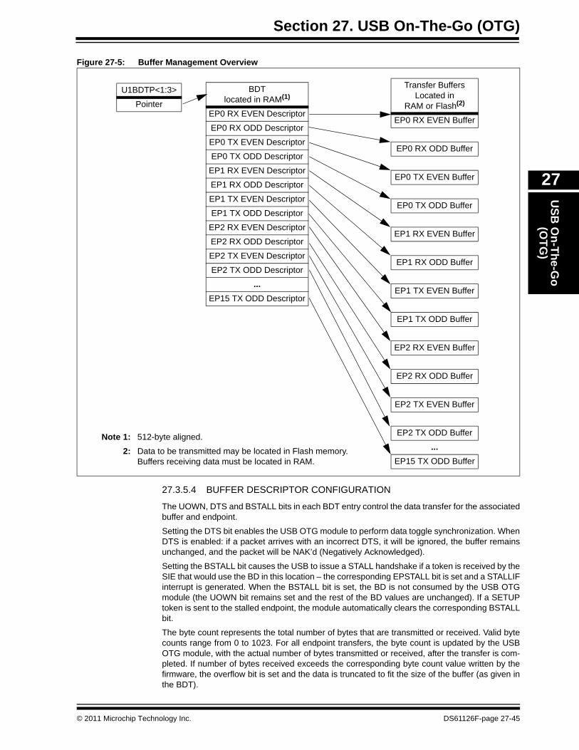
Use of the Buffer Descriptor Table (BDT) allows the buffers to be located anywhere in RAM, andprovides status flags and control bits. The BDT contains the address of each endpoint data buf-fer, as well as information about each buffer (see Figure 27-2, Figure 27-3 and Figure 27-4).Each BDT entry is called a Buffer Descriptor (BD) and is 8 bytes long. Four descriptor entries areused for each endpoint. All endpoints, ranging from endpoint 0 to the highest endpoint in use,must have four descriptor entries. Even if all of the buffers for an endpoint are not used, fourdescriptor entries are required for each endpoint.
The USB OTG module calculates a buffer’s location in memory using the BDT Pointer registers.The base of the BDT is held in registers U1BDTP1 through U1BDTP3. The address of thedesired buffer is found by using the endpoint number, the type (RX/TX) and the ODD/EVEN bitto index into the BDT. The address held by this entry is the address of the desired data buffer.See 27.3.5.3 “Buffer Management”.
Each of the 16 endpoints owns two descriptor pairs: two for packets to transmit, and two for pack-ets received. Each pair manages two buffers, an EVEN and an ODD, requiring a maximum of 64descriptors (16*2*2).
Having EVEN and ODD buffers for each direction allows the CPU to access data in one bufferwhile the USB OTG module transfers data to or from the other buffer. The USB OTG modulealternates between buffers, clearing the UOWN bit in the buffer descriptor automatically whenthe transaction for that buffer is complete. The use of alternating buffers maximizes data through-put by allowing CPU data access in parallel with data transfer. This technique is referred to asping-pong buffering. Figure 27-5 illustrates how the endpoints are mapped in the BDT.
27.3.5.2.1 Endpoint Control Each endpoint is controlled by an Endpoint Control register, U1EPn, that configures the transferdirection, the handshake, and the stalling properties of the endpoint. The Endpoint Controlregister also allows support of control transfers.
27.3.5.2.2 Host Endpoints
The host performs all transactions through a single endpoint (Endpoint 0). All other endpointsshould be disabled and other endpoint buffers are not be used.
27.3.5.2.3 Device EndpointsEndpoint 0 must be implemented for a USB device to be enumerated and controlled. Devicestypically implement additional endpoints to transfer data.
Note: The contents of the U1BDTP1-U1BDTP3 registers provide the upper 23 bits of the32-bit address; therefore, the BDT must be aligned to a 512 byte boundary (seeFigure 27-2). This address must be the physical (not virtual) memory address.
Note: In Host mode, Endpoint 0 has additional bits for auto-retry and hub support.
DS61126F-page 27-40 © 2011 Microchip Technology Inc.

Section 27. USB On-The-Go (OTG)U
SB O
n-The-Go
(OTG
)
27
27.3.5.3 BUFFER MANAGEMENT
The buffers are shared between the CPU and the USB OTG module, and are implemented insystem memory. So, a simple semaphore mechanism is used to distinguish current ownership ofthe BD, and associated buffers, in memory. This semaphore mechanism is implemented by theUOWN bit in each BD.
The USB OTG module clears the UOWN bit automatically when the transaction for that buffer iscomplete. When the UOWN bit is clear, the descriptor is owned by the CPU – which may modifythe descriptor and buffer as necessary.
Software must configure the BDT entry for the next transaction, then set the UOWN bit to returncontrol to the USB OTG module.
A BD is only valid if the corresponding endpoint has been enabled in the U1EPn register. TheBDT is implemented in data memory, and the BDs are not modified when the USB OTG moduleis reset. Initialize the BDs prior to enabling them through the U1EPn. At a minimum, the UOWNbits must be cleared prior to being enabled.
In Host mode, BDT initialization is required before the U1TOK register is written, which triggersa transfer.
Figure 27-2: BDT Address Generation BDTBA<22:0> ENDPOINT<3:0> DIR PPBI FIELD
31:9 8:5 4 3 2:0
bit 31-9 BDTBA<22:0>: BDT Base Address bitsThe 23-bit value is made up of the contents of the U1BDTP3, U1BDTP2 and U1BDTP1 registers.
bit 8-5 ENDPOINT<3:0>: Transfer Endpoint Number bits1111 = Endpoint 151110 = Endpoint 14•••0001 = Endpoint 10000 = Endpoint 0
bit 4 DIR: Transfer Direction bit1 = Transmit: SETUP/OUT for host, IN for function0 = Receive: IN for host, SETUP/OUT for function
bit 3 PPBI: Ping-Pong Pointer bit1 = ODD buffer0 = EVEN buffer
bit 2-0 Manipulated by the USB OTG moduleUsed to access fields within the BD.
© 2011 Microchip Technology Inc. DS61126F-page 27-41

PIC32 Family Reference Manual
27.3.5.3.4 Buffer Descriptor FormatThe buffer descriptor is used in the following formats:
• Control• Status
Buffer descriptor control format, in which software writes the descriptor and hands it to hardware,is shown in Figure 27-3.
Figure 27-3: USB Buffer Descriptor Control Format: Software to Hardware Address Offset +0
31 26 25 16 15 8 7 6 5 4 3 2 1 0
— BYTE_COUNT<9:0> —
UO
WN
DAT
A0/
1K
EEP
NIN
CD
TSB
STA
LL
—
Address Offset +431 0
BUFFER_ADDRESS<31:0>(1)
Address Offset +0bit 31-26 Reservedbit 25-16 BYTE_COUNT<9:0>: Byte Count bits
Byte count represents the number of bytes to be transmitted or the maximum number of bytes to bereceived during a transfer.
bit 15-8 Reservedbit 7 UOWN: USB Own bit
1 = USB OTG module owns the BD and its corresponding bufferCPU must not modify the BD or the buffer.
0 = CPU owns the BD and its corresponding bufferUSB OTG module ignores all other fields in the BD.
USBFRZ is writable in Debug Exception mode only, it is forced to ‘0’ in normal mode.
Note: This bit can be programmed by either the CPU or the USB OTG module, and it must be initializedby the user to the desired value prior to enabling the USB endpoint.
bit 6 DATA0/1: Data Toggle Packet bit1 = Transmit a Data 1 packet or Check received PID = DATA1, if DTS = 10 = Transmit a Data 0 packet or Check received PID = DATA0, if DTS = 1
bit 5 KEEP: BD Keep Enable bit1 = USB will keep the BD indefinitely once UOWN is set
U1STAT FIFO will not be updated and TRNIF bit will not be set at the end of each transaction.0 = USB will hand back the BD once a token has been processed
bit 4 NINC: DMA Address Increment Disable bit1 = DMA address increment disabled0 = DMA address increment enabled
bit 3 DTS: Data Toggle Synchronization Enable bit1 = Data Toggle Synchronization is enabled – data packets with incorrect sync value will be ignored0 = No Data Toggle Synchronization is performed
Note: Expected value of DATA PID (DATA0/DATA1) specified in the DATA0/1 field.
DS61126F-page 27-42 © 2011 Microchip Technology Inc.

Section 27. USB On-The-Go (OTG)U
SB O
n-The-Go
(OTG
)
27
bit 2 BSTALL: Buffer Stall Enable bit1 = Buffer STALL enabled
STALL handshake issued if a token is received that would use the BD in the given location (UOWN bitremains set, BD value is unchanged).Corresponding EPSTALL bit will get set on any STALL handshake.
0 = Buffer STALL disabledbit 1-0 Reserved
Address Offset +4bit 31-0 BUFFER_ADDRESS<31:0>: Buffer Address bits(1)
Starting point address of the endpoint packet data buffer.
Note 1: The individual buffer addresses in the BDT must be physical memory addresses.
© 2011 Microchip Technology Inc. DS61126F-page 27-43

PIC32 Family Reference Manual
Buffer descriptor status format, in which hardware writes the descriptor and hands it back tosoftware, is shown in Figure 27-4.
Figure 27-4: USB Buffer Descriptor Status Format: Hardware to Software Address Offset +0
31 26 25 16 15 8 7 6 5 4 3 2 1 0
— BYTE_COUNT<9:0> —
UO
WN
DAT
A0/
1 PID<3:0> —
Address Offset +4
31 0
BUFFER_ADDRESS<31:0>
Address Offset +0bit 31-26 Reservedbit 25-16 BYTE_COUNT<9:0>: Byte Count bits
Byte count reflects the actual number of bytes received or transmitted.bit 15-8 Reservedbit 7 UOWN: USB Own bit
1 = USB OTG module owns the BD and its corresponding bufferCPU must not modify the BD or the buffer.
0 = CPU owns the BD and its corresponding buffer
Note: This bit can be programmed by either the CPU or the USB OTG module, and it must be initializedby the user to the desired value prior to enabling the USB endpoint.
bit 6 DATA0/1: Data Toggle Packet bit1 = Data 1 packet received0 = Data 0 packet received
Note: This bit is unchanged when a packet is transmitted.bit 5-2 PID<3:0>: Packet Identifier bits
The current token PID when a transfer completes.The values written back are the token PID values from the USB specification: 0x1 for an OUT token, 0x9 for an IN token or 0xd for a SETUP token.In Host mode, this field is used to report the last returned PID or a transfer status indication.The possible values returned are: 0x3 DATA0, 0xb DATA1, 0x2 ACK, 0xe STALL, 0xa NAK, 0x0 Bus Time-out and 0xf Data Error.
bit 1-0 Reserved
Address Offset +4bit 31-0 BUFFER_ADDRESS<31:0>: Buffer Address bits
Starting point address of the endpoint packet data buffer.
DS61126F-page 27-44 © 2011 Microchip Technology Inc.
Section 27. USB On-The-Go (OTG)U
SB O
n-The-Go
(OTG
)
27
Figure 27-5: Buffer Management Overview
27.3.5.4 BUFFER DESCRIPTOR CONFIGURATION
The UOWN, DTS and BSTALL bits in each BDT entry control the data transfer for the associatedbuffer and endpoint.
Setting the DTS bit enables the USB OTG module to perform data toggle synchronization. WhenDTS is enabled: if a packet arrives with an incorrect DTS, it will be ignored, the buffer remainsunchanged, and the packet will be NAK’d (Negatively Acknowledged).
Setting the BSTALL bit causes the USB to issue a STALL handshake if a token is received by theSIE that would use the BD in this location – the corresponding EPSTALL bit is set and a STALLIFinterrupt is generated. When the BSTALL bit is set, the BD is not consumed by the USB OTGmodule (the UOWN bit remains set and the rest of the BD values are unchanged). If a SETUPtoken is sent to the stalled endpoint, the module automatically clears the corresponding BSTALLbit.
The byte count represents the total number of bytes that are transmitted or received. Valid bytecounts range from 0 to 1023. For all endpoint transfers, the byte count is updated by the USBOTG module, with the actual number of bytes transmitted or received, after the transfer is com-pleted. If number of bytes received exceeds the corresponding byte count value written by thefirmware, the overflow bit is set and the data is truncated to fit the size of the buffer (as given inthe BDT).
U1BDTP<1:3>
Pointer
BDTlocated in RAM(1)
EP0 RX EVEN Descriptor
EP0 RX ODD Descriptor
EP0 TX EVEN Descriptor
EP0 TX ODD Descriptor
EP1 RX EVEN Descriptor
EP1 RX ODD Descriptor
EP1 TX EVEN Descriptor
EP1 TX ODD Descriptor
EP2 RX EVEN Descriptor
EP2 RX ODD Descriptor
EP2 TX EVEN Descriptor
EP2 TX ODD Descriptor
...EP15 TX ODD Descriptor
Transfer BuffersLocated in
RAM or Flash(2)
EP0 RX EVEN Buffer
EP0 RX ODD Buffer
EP0 TX EVEN Buffer
EP0 TX ODD Buffer
EP1 RX EVEN Buffer
EP1 RX ODD Buffer
EP1 TX EVEN Buffer
EP1 TX ODD Buffer
EP2 RX EVEN Buffer
EP2 RX ODD Buffer
EP2 TX EVEN Buffer
EP2 TX ODD Buffer
...EP15 TX ODD Buffer
Note 1: 512-byte aligned.
2: Data to be transmitted may be located in Flash memory.Buffers receiving data must be located in RAM.
© 2011 Microchip Technology Inc. DS61126F-page 27-45
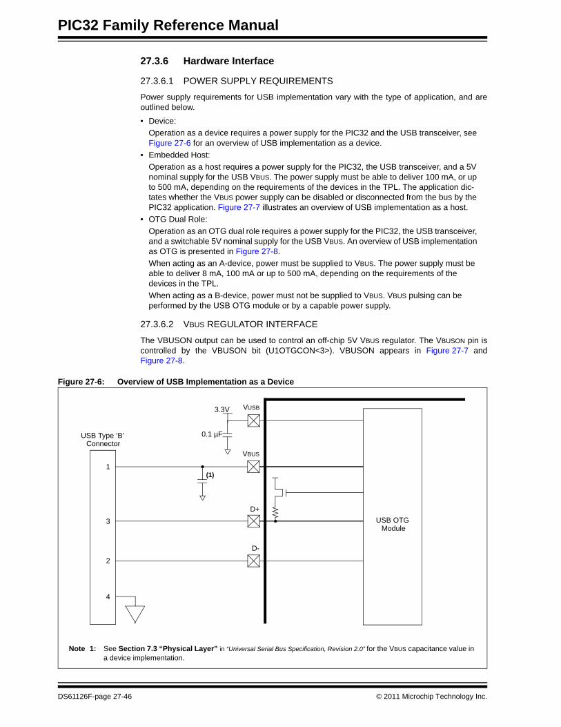
PIC32 Family Reference Manual
27.3.6 Hardware Interface
27.3.6.1 POWER SUPPLY REQUIREMENTS
Power supply requirements for USB implementation vary with the type of application, and areoutlined below.
• Device:Operation as a device requires a power supply for the PIC32 and the USB transceiver, see Figure 27-6 for an overview of USB implementation as a device.
• Embedded Host:Operation as a host requires a power supply for the PIC32, the USB transceiver, and a 5V nominal supply for the USB VBUS. The power supply must be able to deliver 100 mA, or up to 500 mA, depending on the requirements of the devices in the TPL. The application dic-tates whether the VBUS power supply can be disabled or disconnected from the bus by the PIC32 application. Figure 27-7 illustrates an overview of USB implementation as a host.
• OTG Dual Role:Operation as an OTG dual role requires a power supply for the PIC32, the USB transceiver, and a switchable 5V nominal supply for the USB VBUS. An overview of USB implementation as OTG is presented in Figure 27-8. When acting as an A-device, power must be supplied to VBUS. The power supply must be able to deliver 8 mA, 100 mA or up to 500 mA, depending on the requirements of the devices in the TPL. When acting as a B-device, power must not be supplied to VBUS. VBUS pulsing can be performed by the USB OTG module or by a capable power supply.
27.3.6.2 VBUS REGULATOR INTERFACE
The VBUSON output can be used to control an off-chip 5V VBUS regulator. The VBUSON pin iscontrolled by the VBUSON bit (U1OTGCON<3>). VBUSON appears in Figure 27-7 andFigure 27-8.
Figure 27-6: Overview of USB Implementation as a Device
VUSB
D+
D-
VBUS
USB OTG
USB Type ‘B’Connector
2
3
1
4
3.3V
0.1 µF
(1)
Note 1: See Section 7.3 “Physical Layer” in “Universal Serial Bus Specification, Revision 2.0” for the VBUS capacitance value ina device implementation.
Module
DS61126F-page 27-46 © 2011 Microchip Technology Inc.
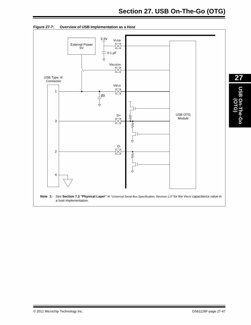
Section 27. USB On-The-Go (OTG)U
SB O
n-The-Go
(OTG
)
27
Figure 27-7: Overview of USB Implementation as a Host
VUSB
D+
D-
VBUS
USB OTG
External Power
USB Type ‘A’Connector
2
3
1
4
VBUSON
5V
3.3V
0.1 µF
(1)
Note 1: See Section 7.3 “Physical Layer” in “Universal Serial Bus Specification, Revision 2.0” for the VBUS capacitance value ina host implementation.
Module
© 2011 Microchip Technology Inc. DS61126F-page 27-47
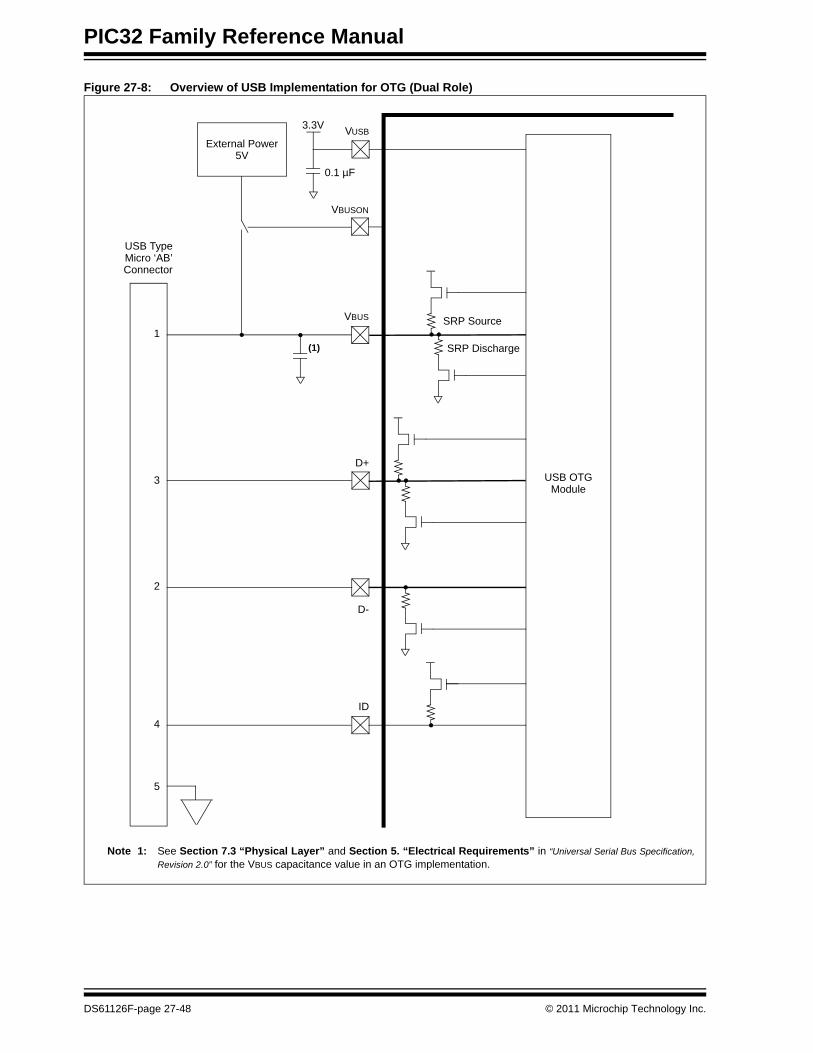
PIC32 Family Reference Manual
Figure 27-8: Overview of USB Implementation for OTG (Dual Role)
VUSB
D+
D-
VBUS
USB OTG
External Power
2
3
1
5
VBUSON
5V
SRP Source
SRP Discharge
4ID
3.3V
USB TypeMicro ‘AB’Connector
0.1 µF
(1)
Note 1: See Section 7.3 “Physical Layer” and Section 5. “Electrical Requirements” in “Universal Serial Bus Specification,Revision 2.0” for the VBUS capacitance value in an OTG implementation.
Module
DS61126F-page 27-48 © 2011 Microchip Technology Inc.
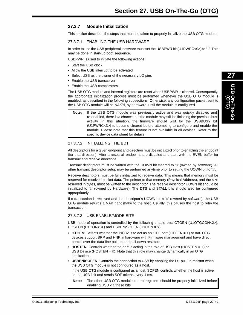
Section 27. USB On-The-Go (OTG)U
SB O
n-The-Go
(OTG
)
27
27.3.7 Module InitializationThis section describes the steps that must be taken to properly initialize the USB OTG module.
27.3.7.1 ENABLING THE USB HARDWARE
In order to use the USB peripheral, software must set the USBPWR bit (U1PWRC<0>) to ‘1’. Thismay be done in start-up boot sequence.
USBPWR is used to initiate the following actions:
• Start the USB clock• Allow the USB interrupt to be activated• Select USB as the owner of the necessary I/O pins• Enable the USB transceiver• Enable the USB comparators
The USB OTG module and internal registers are reset when USBPWR is cleared. Consequently,the appropriate initialization process must be performed whenever the USB OTG module isenabled, as described in the following subsections. Otherwise, any configuration packet sent tothe USB OTG module will be NAK’d, by hardware, until the module is configured.
27.3.7.2 INITIALIZING THE BDT
All descriptors for a given endpoint and direction must be initialized prior to enabling the endpoint(for that direction). After a reset, all endpoints are disabled and start with the EVEN buffer fortransmit and receive directions.
Transmit descriptors must be written with the UOWN bit cleared to ‘0’ (owned by software). Allother transmit descriptor setup may be performed anytime prior to setting the UOWN bit to ‘1’.
Receive descriptors must be fully initialized to receive data. This means that memory must bereserved for received packet data. The pointer to that memory (Physical Address), and the sizereserved in bytes, must be written to the descriptor. The receive descriptor UOWN bit should beinitialized to ‘1’ (owned by Hardware). The DTS and STALL bits should also be configuredappropriately.
If a transaction is received and the descriptor’s UOWN bit is ‘0’ (owned by software), the USBOTG module returns a NAK handshake to the host. Usually, this causes the host to retry thetransaction.
27.3.7.3 USB ENABLE/MODE BITS
USB mode of operation is controlled by the following enable bits: OTGEN (U1OTGCON<2>),HOSTEN (U1CON<3>) and USBEN/SOFEN (U1CON<0>).
• OTGEN: Selects whether the PIC32 is to act as an OTG part (OTGEN = 1) or not. OTG devices support SRP and HNP in hardware with Firmware management and have direct control over the data-line pull-up and pull-down resistors.
• HOSTEN: Controls whether the part is acting in the role of USB Host (HOSTEN = 1) or USB Device (HOSTEN = 0). Note that this role may change dynamically in an OTG application.
• USBEN/SOFEN: Controls the connection to USB by enabling the D+ pull-up resistor when the USB OTG module is not configured as a host.If the USB OTG module is configured as a host, SOFEN controls whether the host is active on the USB link and sends SOF tokens every 1 ms.
Note: If the USB OTG module was previously active and was quickly disabled andre-enabled, there is a chance that the module may still be finishing the previous busactivity. In this situation, the firmware should wait for the USBBUSY bit(U1PWRC<3>) to become cleared before attempting to configure and enable themodule. Please note that this feature is not available in all devices. Refer to thespecific device data sheet for details.
Note: The other USB OTG module control registers should be properly initialized beforeenabling USB via these bits.
© 2011 Microchip Technology Inc. DS61126F-page 27-49

PIC32 Family Reference Manual
27.3.8 Device OperationAll communication on the USB is initiated by the host. Therefore, in device mode, when USB isenabled USBEN = 1 (U1CON<0>), endpoint 0 must be ready to receive control transfers. Initial-ization of the remaining endpoints, descriptors and buffers can be delayed until the host selectsa configuration for the device. Refer to Chapter 9 of “Universal Serial Bus Specification,Revision 2.0” for more information on this subject.
The following steps are performed to respond to a USB transaction:
1. Software pre-initializes the appropriate BDs, and sets the UOWN bits to ‘1’ to be ready fora transaction.
2. Hardware receives a TOKEN PID (IN, OUT, SETUP) from the USB host, and checks theappropriate BD.
3. If the transaction will be transmitted (IN), the module reads packet data from data memory.4. Hardware receives a DATA PID (DATA0/1), and sends or receives the packet data.5. If a transaction is received (SETUP, OUT), the module writes packet data to data memory.6. The module issues, or waits for, a handshake PID (ACK, NAK, STALL), unless the endpoint
is setup as an isochronous endpoint (EPHSHK bit UEPMx<0> is cleared).7. The module updates the BD, and writes the UOWN bit to ‘0’ (SW owned).8. The module updates the U1STAT register, and sets the TRNIF interrupt.9. Software reads the U1STAT register, and determines the endpoint and direction for the
transaction.10. Software reads the appropriate BD, completes all necessary processing, and clears the
TRNIF interrupt.
27.3.8.1 RECEIVING AN IN TOKEN IN DEVICE MODE
Perform the following steps when an IN token is received in Device mode:
1. Attach to a USB host and enumerate as described in Chapter 9 of “Universal Serial BusSpecification, Revision 2.0”.
2. Populate the data buffer with the data to send to the host. 3. In the appropriate (EVEN or ODD) transmit buffer descriptor for the desired endpoint:
a) Set up the control bit fields with the correct data toggle (DATA0/1) value and the bytecount of the data buffer.
b) Set up the address bit field with the starting address of the data buffer.c) Set the UOWN bit field to ‘1’.
4. When the USB OTG module receives an IN token, it automatically transmits the data inthe buffer. Upon completion, the module updates the status bit fields, and sets the transfercomplete interrupt bit, TRNIF(U1IR<3>).
27.3.8.2 RECEIVING AN OUT TOKEN IN DEVICE MODE
Perform the following steps when an OUT token is received in Device mode:
1. Attach to a USB host and enumerate as described in Chapter 9 of “Universal Serial BusSpecification, Revision 2.0”.
2. Create a data buffer with the amount of data you are expecting from the host. 3. In the appropriate (EVEN or ODD) transmit buffer descriptor for the desired endpoint:
a) Set up the control bit fields with the correct data toggle (DATA0/1) value and the bytecount of the data buffer.
b) Set up the address bit field with the starting address of the data buffer.c) Set the UOWN bit of the control bit field to ‘1’.
4. When the USB OTG module receives an OUT token, it will automatically transfer the datathe host sent into the buffer. Upon completion, the module updates the status bit fields,and sets the transfer complete interrupt bit, TRNIF(U1IR<3>).
Note: For transmitted (IN) transactions (host reading data from the device), the read datamust be ready when the Host begins USB signaling. Otherwise, the USB OTGmodule will send a NAK handshake if UOWN is ‘0’.
DS61126F-page 27-50 © 2011 Microchip Technology Inc.
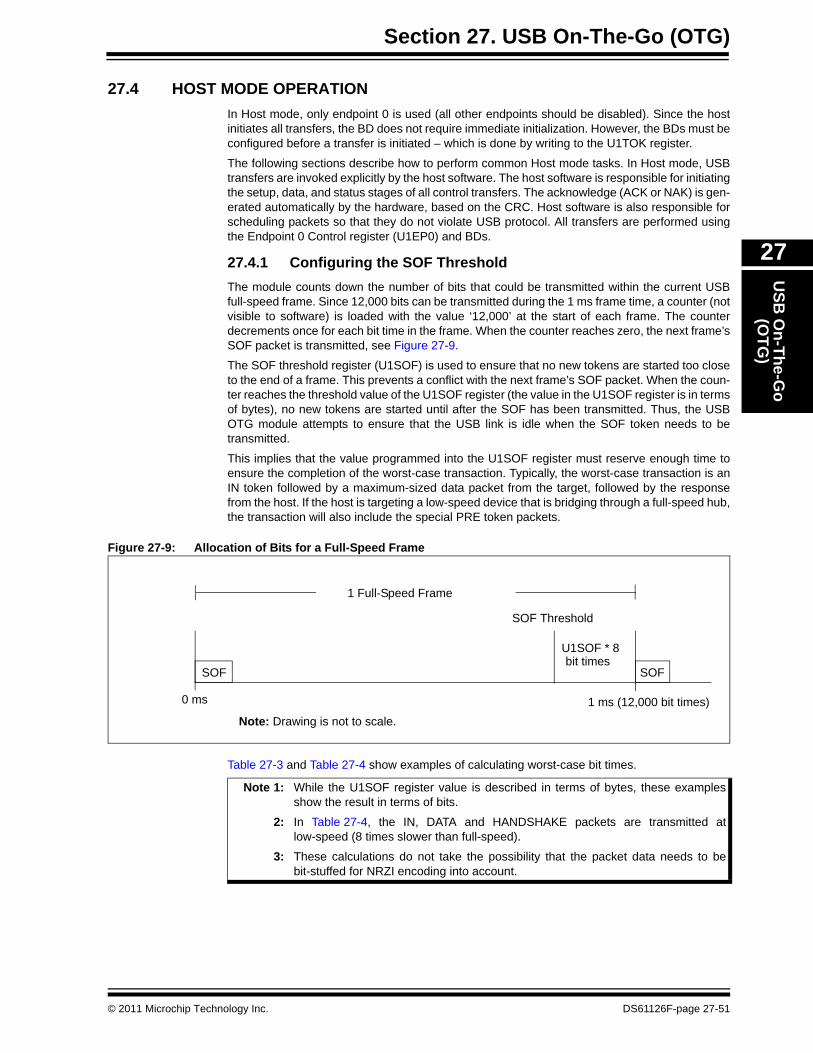
Section 27. USB On-The-Go (OTG)U
SB O
n-The-Go
(OTG
)
27
27.4 HOST MODE OPERATION In Host mode, only endpoint 0 is used (all other endpoints should be disabled). Since the hostinitiates all transfers, the BD does not require immediate initialization. However, the BDs must beconfigured before a transfer is initiated – which is done by writing to the U1TOK register.
The following sections describe how to perform common Host mode tasks. In Host mode, USBtransfers are invoked explicitly by the host software. The host software is responsible for initiatingthe setup, data, and status stages of all control transfers. The acknowledge (ACK or NAK) is gen-erated automatically by the hardware, based on the CRC. Host software is also responsible forscheduling packets so that they do not violate USB protocol. All transfers are performed usingthe Endpoint 0 Control register (U1EP0) and BDs.
27.4.1 Configuring the SOF Threshold The module counts down the number of bits that could be transmitted within the current USBfull-speed frame. Since 12,000 bits can be transmitted during the 1 ms frame time, a counter (notvisible to software) is loaded with the value ‘12,000’ at the start of each frame. The counterdecrements once for each bit time in the frame. When the counter reaches zero, the next frame’sSOF packet is transmitted, see Figure 27-9.
The SOF threshold register (U1SOF) is used to ensure that no new tokens are started too closeto the end of a frame. This prevents a conflict with the next frame’s SOF packet. When the coun-ter reaches the threshold value of the U1SOF register (the value in the U1SOF register is in termsof bytes), no new tokens are started until after the SOF has been transmitted. Thus, the USBOTG module attempts to ensure that the USB link is idle when the SOF token needs to betransmitted.
This implies that the value programmed into the U1SOF register must reserve enough time toensure the completion of the worst-case transaction. Typically, the worst-case transaction is anIN token followed by a maximum-sized data packet from the target, followed by the responsefrom the host. If the host is targeting a low-speed device that is bridging through a full-speed hub,the transaction will also include the special PRE token packets.
Figure 27-9: Allocation of Bits for a Full-Speed Frame
Table 27-3 and Table 27-4 show examples of calculating worst-case bit times.
SOF SOF
U1SOF * 8bit times
0 ms 1 ms (12,000 bit times)Note: Drawing is not to scale.
SOF Threshold
1 Full-Speed Frame
Note 1: While the U1SOF register value is described in terms of bytes, these examplesshow the result in terms of bits.
2: In Table 27-4, the IN, DATA and HANDSHAKE packets are transmitted atlow-speed (8 times slower than full-speed).
3: These calculations do not take the possibility that the packet data needs to bebit-stuffed for NRZI encoding into account.
© 2011 Microchip Technology Inc. DS61126F-page 27-51

PIC32 Family Reference Manual
.
Table 27-3: Example of SOF Threshold Calculation: Full-SpeedPacket Fields Bits
IN SYNC, PID, ADDR, ENDP, CRC5, EOP 35
Turnaround(1) — 8
DATA SYNC, PID, DATA(2), CRC16, EOP 547
Turnaround — 2
HANDSHAKE SYNC, PID, EOP 19
Inter-packet — 2
Total 613
Note 1: Inter-packet delay of 2. An additional 5.5 bit times of latency is added to represent a worst-case propagation delay through 5 hubs.
2: Using 64 bytes maximum packet size for this example calculation.
Table 27-4: Example of SOF Threshold Calculation: Low-Speed Via HubPacket Fields Bits FS Bits
PRE SYNC, PID 16 16
Hub setup — 4 4
IN SYNC, PID, ADDR, ENDP, CRC5, EOP 35 280
Turnaround(1) — 8 8
DATA SYNC, PID, DATA(2), CRC16, EOP 99 792
Turnaround — 2 2
PRE SYNC, PID 16 16
HANDSHAKE SYNC, PID, EOP 19 152
Inter-packet — 2 2
Total 1272
Note 1: Inter-packet delay of 2. An additional 5.5 bit times of latency is added to represent a worst-case propagation delay through 5 hubs.
2: Packets limited to 8 bytes maximum in Low-Speed mode.
Note: Refer to Section 5.11.3 “Calculating Bus Transaction Times” in “Universal Serial Bus Specification,Revision 2.0” for details on calculating bus transaction time.
DS61126F-page 27-52 © 2011 Microchip Technology Inc.

Section 27. USB On-The-Go (OTG)U
SB O
n-The-Go
(OTG
)
27
27.4.2 Enabling Host Mode and Discovering a Connected DeviceTo enable Host mode, perform the following steps:
1. Enable Host mode, the HOSTEN bit (U1CON<3>) = 1. This enables the D+ and D- pull-down resistors, and disables the D+ and D- pull-upresistors. To reduce noise on the bus, disable the SOF packet generation by writing theSOF enable bit to ‘0’, the SOFEN bit (U1CON<0>) = 0.
2. Enable the device attach interrupt, the ATTACHIE bit (U1IE<6> = 1). 3. Wait for the device attach interrupt, the ATTACHIF bit (U1IR<6>).
This is signaled by the USB device changing the state of D+ or D- from ‘0’ to ‘1’ (SE0 toJSTATE). After it occurs, wait for the device power to stabilize (10 ms is minimum, 100 msis recommended).
4. Check the state of the JSTATE and SE0 bits in the control register U1CON. If the JSTATE bit (U1CON<7>) is ‘0’, the connecting device is low-speed; otherwise, thedevice is full-speed.
5. If the connecting device is low-speed, set the low-speed enable bit in the address register,the LSPDEN bit (U1ADDR<7>= 1), and the low-speed bit in the Endpoint 0 Controlregister, the LSPD bit (U1EP0<7> = 1). But, if the device is full-speed, clear these bits.
6. Reset the USB device by sending the Reset signaling for at least 50 ms (USBRST bit(U1CON<4>) = 1). After 50 ms, terminate the Reset (USBRST bit (U1CON<4>) = 0).
7. Enable SOF packet generation to keep the connected device from going into Suspend(SOFEN bit (U1CON<0>) = 1).
8. Wait 10 ms for the device to recover from Reset.9. Perform enumeration as described in Chapter 9 of “Universal Serial Bus Specification,
Revision 2.0”.
27.4.2.1 HOST TRANSACTIONS
When acting as a host, a transaction consists of the following:
1. Software configures the appropriate BD, and sets the UOWN bit to ‘1’ (HW owned).2. Software checks the state of the TOKBUSY bit (U1CON<5>) to verify that any previous
transaction has completed.3. Software writes the address of the target device in the U1ADDR register.4. Software writes the endpoint number and the desired TOKEN PID (IN, OUT or SETUP) to
the U1TOK register.5. Hardware reads the BD to determine the appropriate action, and to obtain the pointer to
data memory.6. Hardware issues the correct TOKEN PID (IN, OUT, SETUP) on the USB link.7. If the transaction is a transmit transaction (OUT, SETUP), the USB OTG module reads the
packet data out of data memory. Then the module follows with the desired DATA PID(DATA0/DATA1) and packet data.
8. If the transaction is a receive transaction (IN), the USB OTG module waits to receive theDATA PID and packet data. Hardware writes the packet data to memory.
9. Hardware issues or waits for a Handshake PID (ACK, NAK or STALL), unless the endpointis set up as an Isochronous Endpoint (EPHSHK bit (U1EPx<0>) is cleared).
10. Hardware updates the BD, and writes the UOWN bit to ‘0’ (SW owned).11. Hardware updates the U1STAT register, and sets the TRNIF bit (U1IR<3>) interrupt.12. Hardware reads the next BD (EVEN or ODD) to see whether it is owned by the USB OTG
module. If it is, hardware begins the next transaction.13. Software should read the U1STAT register, and then clear the TRNIF interrupt.
If Software does not set the UOWN bit to ‘1’ in the appropriate BD prior to writing the U1TOKregister, the module will read the descriptor and do nothing.
© 2011 Microchip Technology Inc. DS61126F-page 27-53
PIC32 Family Reference Manual
27.4.3 Completing a Control Transaction to a Connected DeviceComplete all of the following steps to discover a connected device:
1. Set up the Endpoint Control register for bidirectional control transfers,U1EP0<4:0> = 0x0D.
2. Place an 8-byte device setup packet in the appropriate memory buffer. See Chapter 9 of“Universal Serial Bus Specification, Revision 2.0” for information on the device frameworkcommand set.
3. Initialize the current (EVEN or ODD) TX EP0 BD to transfer the 8-byte device frameworkcommand (for example, a GET DEVICE DESCRIPTOR command). a) Set the BD control offset 0 to 0x8008 (UOWN bit set, byte count of 8).b) Set the BD data buffer address (BD0ADR) to the starting address of the 8-byte
memory buffer containing the command, if it is not already initialized.4. Set the USB address of the target device in the address register U1ADDR<6:0>. After a
USB bus Reset, the device USB address will be zero. After enumeration, it must be set toanother value, between 1 and 127, by the host software.
5. Write the token register with a SETUP command to Endpoint 0, the target device’s defaultcontrol pipe (U1TOK = 0xD0). This will initiate a SETUP token on the bus followed by adata packet. The device handshake will be returned in the PID field of BD status after thepackets complete. When the module updates BD status, a transfer done interrupt will beasserted (U1IR<TRNIF>). This completes the setup stage of the setup transfer asdescribed in Chapter 9 of the USB specification.
6. To initiate the data stage of the setup transaction (for example, get the data for the GETDEVICE DESCRIPTOR command), set up a buffer in memory to store the received data.
7. Initialize the current (EVEN or ODD) RX or TX (RX for IN, TX for OUT) EP0 BD to transferthe data. a) Set the BD control UOWN bit to ‘1’, data toggle (DTS) to DATA1 and byte count to the
length of the data buffer. b) Set the BD data buffer address (BD0ADR) to the starting address of the data buffer
if it is not already initialized.8. Write the Token register with the appropriate IN or OUT token to Endpoint 0 (the target
device’s default control pipe), for example, an IN token for a GET DEVICE DESCRIPTORcommand (U1TOK = 0x90). This will initiate an IN token on the bus followed by a datapacket from the device to the host. When the data packet completes, the BD status is writtenand a transfer done interrupt will be asserted (TRNIF bit (U1IR<3>)). For control transferswith a single packet data phase, this completes the data phase of the setup transaction. Ifmore data needs to be transferred, return to step 6.
9. To initiate the status stage of the setup transaction, set up a buffer in memory to receiveor send the zero length status phase data packet.
10. Initialize the current (EVEN or ODD) TX EP0 BD to transfer the status data. a) Set the BD control to 0x8000 (UOWN bit to ‘1’, data toggle (DTS) to DATA0 and byte
count to ‘0’). b) Set the BDT buffer address field to the start address of the data buffer.
11. Write the Token register with the appropriate IN or OUT token to Endpoint 0, (the targetdevice’s default control pipe) for example, an OUT token for a GET DEVICE DESCRIPTORcommand (U1TOK = 0x10). This will initiate a token on the bus, followed by a zero lengthdata packet from the host to the device. When the data packet completes, the BD isupdated with the handshake from the device, and a transfer done interrupt (TRNIF bit(U1IR<3>)) will be asserted . This completes the status phase of the setup transaction.
Note: Some devices can only effectively respond to one transaction per frame.
DS61126F-page 27-54 © 2011 Microchip Technology Inc.
Section 27. USB On-The-Go (OTG)U
SB O
n-The-Go
(OTG
)
27
27.4.4 Data Transfer with a Target DeviceComplete all of the following steps to discover and configure a connected device.
1. Write the EP0 Control register (U1EPn) to enable transmit and receive transfers as appro-priate with handshaking enabled (unless isochronous transfers are to be used). If the tar-get device is a low-speed device, also set the Low-Speed Enable bit, the LSPD bit(U1EPn<7>). If you want the hardware to automatically retry indefinitely if the targetdevice asserts a NAK on the transfer, clear the Retry Disable bit, RETRYDIS (U1EPn<6>).
2. Set up the current Buffer Descriptor (EVEN or ODD) in the appropriate direction to transferthe desired number of bytes.
3. Set the address of the target device in the address register (U1ADDR<6:0>). 4. Write the Token register (U1TOK) with an IN or OUT token as appropriate for the desired
endpoint. This triggers the module’s transmit state machines to begin transmitting thetoken and the data.
5. Wait for the transfer done interrupt (TRNIF bit (U1IR<3>)). This will indicate that the BDhas been released back to the microprocessor and the transfer has completed. If the retrydisable bit is set, the handshake (ACK, NAK, STALL or ERROR (0xf)) will be returned inthe BD PID field. If a stall interrupt occurs, then the pending packet must be dequeued andthe error condition in the target device cleared. If a detach interrupt occurs (SE0 for morethan 2.5 μs), then the target has detached (DETACHIF bit (U1IR<0>)).
6. Once the transfer done interrupt (TRNIF bit (U1IR<3>)) occurs, the BD can be examinedand the next data packet queued by returning to step 2.
27.4.4.1 USB LINK STATES
Three possible link states are described in the following subsections:
• Reset• Idle and Suspend• Resume Signaling
27.4.4.1.1 ResetAs a host, software is required to drive Reset signaling. It may do this by setting the USBRST bit(U1CON<4>). As per the USB specification, the host must drive the Reset for at least 50 ms. (Thisdoes not have to be continuous Reset signaling. Refer to “Universal Serial Bus Specification, Revi-sion 2.0” for more information.) Following Reset, the host must not initiate any downstream trafficfor another 10 ms.
As a device, the USB OTG module will assert the URSTIF bit (U1IR<0>) interrupt when it hasdetected Reset signaling for 2.5 μs. Software must perform any Reset initialization processing atthis time. This includes setting the Address register to 0x00 and enabling Endpoint 0. TheURSTIF interrupt will not be set again until the Reset signaling has gone away and then has beendetected again for 2.5 μs.
Note: Use of automatic indefinite retries can lead to a deadlock condition if the devicenever responds.
Note: USB speed, transceiver and pull-ups should only be configured during the modulesetup phase. It is not recommended to change these settings while the module isenabled.
© 2011 Microchip Technology Inc. DS61126F-page 27-55
PIC32 Family Reference Manual
27.4.4.1.2 Idle and SuspendThe Idle state of the USB is a constant J state. When the USB has been Idle for 3 ms, a deviceshould go into Suspend state. During active operation, the USB host will send a SOF token every1 ms, preventing a device from going into Suspend state.
Once the USB link is in the Suspend state, a USB host or device must drive resume signalingprior to initiating any bus activity. (The USB link may also be disconnected).
As a USB host, software should consider the link in Suspend state as soon as software clearsthe SOFEN bit (U1CON<0>).
As a USB device, hardware will set the IDLEIF bit (U1IR<4>) interrupt when it detects a constantIdle on the bus for 3 ms. Software should consider the link in Suspend state when the IDLEIFinterrupt is set.
When a Suspend condition has been detected, the software may wish to place the USB hard-ware in a Suspend mode by setting the USUSPEND bit (U1PWRC<1>). The hardware Suspendmode gates the USB OTG module’s 48 MHz clock and places the USB transceiver in aLow-Power mode.
Additionally, the user may put the PIC32 into Sleep mode while the link is suspended.
27.4.4.1.3 Driving Resume SignalingIf software wants to wake the USB from Suspend state, it may do so by setting the RESUME bit(U1CON<2>). This will cause the hardware to generate the proper resume signaling (includingfinishing with a low-speed EOP if in host mode).
A USB device should not drive resume signaling unless the Idle state has persisted for at least5 ms. The USB host also must have enabled the function for remote wake-up.
Software must set RESUME for 1-15 ms if a USB device, or greater than 20 ms if a USB host,then clear it to enable remote wake-up. For more information on RESUME signaling, seeSection 7.1.7.7, 11.9, and 11.4.4 in “Universal Serial Bus Specification, Revision 2.0”.
Writing RESUME will automatically clear the special hardware Suspend (low-power) state.
If the part is acting as a USB host, software should, at minimum, set the SOFEN bit (U1CON<0>)after driving its resume signaling. Otherwise, the USB link would return right back to the Suspendstate after 3 ms of inactivity. Also, software must not initiate any downstream traffic for 10 msfollowing the end of resume signaling.
27.4.4.1.4 Receiving Resume SignalingWhen the USB logic detects resume signaling on the USB bus for 2.5 μs, hardware will set theresume interrupt bit, RESUMEIF (U1IR<5>).
A device receiving resume signaling must prepare itself to receive normal USB activity. A hostreceiving resume signaling must immediately start driving resume signaling of its own. Thespecial hardware Suspend (low-power) state is automatically cleared upon receiving any activityon the USB link.
Reception of any activity on the USB link (this may be due to resume signaling or a link discon-nect) while the PIC32 is in Sleep mode will cause the ACTVIF bit (U1OTGIR<4>) interrupt to beset. This will cause wake-up from Sleep.
27.4.4.2 SRP SUPPORT
SRP support is not required by non-OTG applications. SRP may only be initiated at full-speed.Refer to the On-The-Go Supplement specification for more information regarding SRP.
An OTG A-device or embedded host may decide to power-down the VBUS supply when it is notusing the USB link. Software may do this by clearing the VBUSON bit (U1OTGCON<3>). Whenthe VBUS supply is powered down, the A-device is said to have ended a USB session.
Note: When the A-device powers down the VBUS supply, the B-device must disconnect itspull-up resistor.
DS61126F-page 27-56 © 2011 Microchip Technology Inc.

Section 27. USB On-The-Go (OTG)U
SB O
n-The-Go
(OTG
)
27
An OTG A-device or embedded host may repower the VBUS supply at any time to initiate a newsession. An OTG B-device may also request that the OTG A-device repower the VBUS supply toinitiate a new session. This is the purpose of the SRP.
Prior to requesting a new session, the B-device must first check that the previous session hasdefinitely ended. To do this, the B-device must check that:
1. VBUS supply is below the session end voltage.2. Both D+ and D- have been low for at least 2 ms.
The B-device will be notified of condition 1 by the SESENDIF bit (U1OTGIR<2>) interrupt.
Software can use the LSTATEIF bit (U1OTGIR<5>) and the 1 ms timer to identify condition 2.
The B-device may aid in achieving condition 1 by discharging the VBUS supply through a resistor.Software may do this by setting the VBUSDIS bit (U1OTGCON<0>).
After these initial conditions are met, the B-device may begin requesting the new session. TheB-device then proceeds by pulsing the D+ data line. Software should do this by setting the DPPULUPbit (U1OTGCON<7>). The data line should be held high for 5-10 ms.
After data line pulsing, the B-device should complete SRP signaling by pulsing the VBUS supply.This should be done in software by setting the VBUSCHG bit (U1OTGCON<1>).
When an A-device detects SRP signaling (either via the ATTACHIF bit (U1IR<6>) interrupt or viathe SESVDIF bit (U1OTGIR<3>) interrupt), the A-device must restore the VBUS supply by settingthe VBUSON bit (U1OTGCON<3>).
The B-device should not monitor the state of the VBUS supply while performing VBUS supplypulsing. Afterwards, if the B-device does detect that the VBUS supply has been restored (via theSESVDIF bit (U1OTGIR<3>) interrupt), it must reconnect to the USB link by pulling up D+. TheA-device must complete the SRP by enabling VBUS and driving Reset signaling.
Refer to the On-The-Go supplement in “Universal Serial Bus Specification, Revision 2.0” foradditional details.
27.4.4.3 HNP
An OTG application with a micro-AB receptacle must support HNP. The HNP allows an OTGB-device to temporarily become the USB host. The A-device must first enable HNP in theB-device. The HNP may only be initiated at full-speed.
After being enabled for HNP by the A-device, the B-device can request to become the host anytime that the USB link is in Suspend state by simply indicating a disconnect. Software mayaccomplish this by clearing the DPPULUP bit (U1OTGCON<7>).
When the A-device detects the disconnect condition (via the URSTIF (U1IR<0>) interrupt), theA-device may allow the B-device to take over as host. The A-device does this by signalingconnect as a full-speed device. Software may accomplish this by disabling host operation,HOSTEN = 0 (U1CON<3>), and connecting as a device (USB_EN = 1). If the A-device insteadresponds with resume signaling, the A-device will remain as host.
When the B-device detects the connect condition (via the ATTACHIF bit (U1IR<6>)), theB-device becomes host. The B-device drives Reset signaling prior to using the bus.
When the B-device has finished in its role as host, it stops all bus activity and turns on its D+pull-up resistor by disabling host operations (HOSTEN = 0) and reconnecting as a device(USB_EN = 1).
© 2011 Microchip Technology Inc. DS61126F-page 27-57
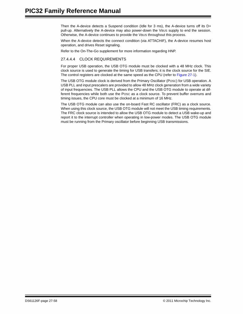
PIC32 Family Reference Manual
Then the A-device detects a Suspend condition (Idle for 3 ms), the A-device turns off its D+pull-up. Alternatively the A-device may also power-down the VBUS supply to end the session.Otherwise, the A-device continues to provide the VBUS throughout this process.
When the A-device detects the connect condition (via ATTACHIF), the A-device resumes hostoperation, and drives Reset signaling.
Refer to the On-The-Go supplement for more information regarding HNP.
27.4.4.4 CLOCK REQUIREMENTS
For proper USB operation, the USB OTG module must be clocked with a 48 MHz clock. Thisclock source is used to generate the timing for USB transfers; it is the clock source for the SIE.The control registers are clocked at the same speed as the CPU (refer to Figure 27-1).
The USB OTG module clock is derived from the Primary Oscillator (POSC) for USB operation. AUSB PLL and input prescalers are provided to allow 48 MHz clock generation from a wide varietyof input frequencies. The USB PLL allows the CPU and the USB OTG module to operate at dif-ferent frequencies while both use the POSC as a clock source. To prevent buffer overruns andtiming issues, the CPU core must be clocked at a minimum of 16 MHz.
The USB OTG module can also use the on-board Fast RC oscillator (FRC) as a clock source.When using this clock source, the USB OTG module will not meet the USB timing requirements.The FRC clock source is intended to allow the USB OTG module to detect a USB wake-up andreport it to the interrupt controller when operating in low-power modes. The USB OTG modulemust be running from the Primary oscillator before beginning USB transmissions.
DS61126F-page 27-58 © 2011 Microchip Technology Inc.
Section 27. USB On-The-Go (OTG)U
SB O
n-The-Go
(OTG
)
27
27.5 INTERRUPTS The USB OTG module uses interrupts to signal USB events such as a change in status, datareceived and buffer empty events, to the CPU. Software must be able to respond to these interruptsin a timely manner.
27.5.1 Interrupt ControlEach interrupt source in the USB OTG module has an interrupt flag bit and a correspondingenable bit. In addition, the UERRIF bit (U1IR<1>) is a logical OR of all the enabled error flagsand is read-only. The UERRIF bit can be used to check the USB OTG module for events whilein an Interrupt Service Routine (ISR).
27.5.2 USB OTG module Interrupt Request GenerationThe USB OTG module can generate interrupt requests from a variety of events. To interfacethese interrupts to the CPU, the USB interrupts are combined such that any enabled USB inter-rupt will cause a generic USB interrupt (if the USB interrupt is enabled) to the interrupt controller,see Figure 27-11. The USB ISR must then determine which USB event(s) caused the CPU inter-rupt and service them appropriately. There are two layers of interrupt registers in the USB OTGmodule. The top level of bits consists of overall USB status interrupts in the U1OTGIR and U1IRregisters. The U1OTGIR and U1IR bits are individually enabled through the corresponding bitsin the U1OTGIE and U1IE registers. In addition, the USB Error Condition bit (UERRIF) passesthrough any interrupt conditions in the U1EIR register enabled via the U1EIE register bits.
27.5.3 Interrupt TimingInterrupts for transfers are generated at the end of the transfer. Figure 27-10 illustrates some typ-ical event sequences that can generate a USB interrupt and when that interrupt is generated.There is no mechanism by which software can manually set an interrupt bit.
The values in the Interrupt Enable registers (U1IE, U1EIE, U1OTGIE) only affect the propagationof an interrupt condition to the CPU’s interrupt controller. Even though an interrupt is not enabled,interrupt flag bits can still be polled and serviced.
27.5.4 Interrupt ServicingOnce an interrupt bit has been set by the USB OTG module (in U1IR, U1EIR or U1OTGIR), itmust be cleared by software by writing a ‘1’ to the appropriate bit position to clear the interrupt.The USB Interrupt bit, USBIF (IFS1<25>), must be cleared before the end of the ISR.
© 2011 Microchip Technology Inc. DS61126F-page 27-59

PIC32 Family Reference Manual
Figure 27-10: Typical Events for USB Interrupts
USB <USBRST>
ACKSETUP TOKEN DATA
URSTIFInterrupt Generated
TRNIFInterrupt Generated
IN TOKEN DATA
ACKOUT TOKEN DATA
TRNIFInterrupt Generated
TRNIFInterrupt Generated
Control
ACK
= Host = Function
SOF
SOFIFInterrupt Generated
DS61126F-page 27-60 © 2011 Microchip Technology Inc.

Section 27. USB On-The-Go (OTG)U
SB O
n-The-Go
(OTG
)
27
Figure 27-11: USB Interrupt Logic
DMAEFDMAEE
BTOEFBTOEE
DFN8EFDFN8EE
CRC16EFCRC16EE
CRC5EF/EOFEFCRC5EE/EOFEE
PIDEFPIDEE
ATTACHIFATTACHIE
RESUMEIFRESUMEIE
IDLEIFIDLEIE
TRNIFTRNIE
SOFIFSOFIE
DETACHIF/URSTIFDETACHIE/URSTIE
USB Interrupt
STALLIF STALLIE
BTSEFBTSEE
T1MSECIFT1MSECIE
LSTATEIFLSTATEIE
ACTVIFACTVIE
SESVDIFSESVDIE
SESENDIFSESENDIE
VBUSVDIFVBUSVDIE
IDIFIDIE
UERRIFUERRIE
BMXEFBMXEE
© 2011 Microchip Technology Inc. DS61126F-page 27-61
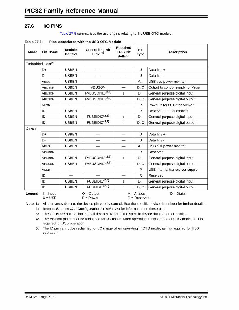
PIC32 Family Reference Manual
27.6 I/O PINSTable 27-5 summarizes the use of pins relating to the USB OTG module.
Table 27-5: Pins Associated with the USB OTG Module
Mode Pin Name Module Control
Controlling Bit Field(1)
Required TRIS Bit Setting
Pin Type Description
Embedded Host(4)
D+ USBEN — — U Data line +
D- USBEN — — U Data line -
VBUS USBEN — — A, I USB bus power monitor
VBUSON USBEN VBUSON — D, O Output to control supply for VBUS
VBUSON USBEN FVBUSONIO(2,3) 1 D, I General purpose digital input
VBUSON USBEN FVBUSONIO(2,3) 0 D, O General purpose digital output
VUSB — — — P Power in for USB transceiver
ID USBEN — — R Reserved; do not connect
ID USBEN FUSBIDIO(2,3) 1 D, I General purpose digital input
ID USBEN FUSBIDIO(2,3) 0 D, O General purpose digital output
Device
D+ USBEN — — U Data line +
D- USBEN — — U Data line -
VBUS USBEN — — A, I USB bus power monitor
VBUSON — — — R Reserved
VBUSON USBEN FVBUSONIO(2,3) 1 D, I General purpose digital input
VBUSON USBEN FVBUSONIO(2,3) 0 D, O General purpose digital output
VUSB — — — P USB internal transceiver supply
ID — — — R Reserved
ID USBEN FUSBIDIO(2,3) 1 D, I General purpose digital input
ID USBEN FUSBIDIO(2,3) 0 D, O General purpose digital output
Legend: I = Input O = Output A = Analog D = DigitalU = USB P = Power R = Reserved
Note 1: All pins are subject to the device pin priority control. See the specific device data sheet for further details.2: Refer to Section 32. “Configuration” (DS61124) for information on these bits.3: These bits are not available on all devices. Refer to the specific device data sheet for details.4: The VBUSON pin cannot be reclaimed for I/O usage when operating in Host mode or OTG mode, as it is
required for USB operation.5: The ID pin cannot be reclaimed for I/O usage when operating in OTG mode, as it is required for USB
operation.
DS61126F-page 27-62 © 2011 Microchip Technology Inc.

Section 27. USB On-The-Go (OTG)U
SB O
n-The-Go
(OTG
)
27
OTG(4,5)
D+ USBEN — — U Data line +
D- USBEN — — U Data line -
VBUS USBEN VBUSCHG, VBUSDIS
— A, I/O USB bus power monitor
VBUSON USBEN VBUSCHG, VBUSDIS, VBUSON
— D, O USB Host and OTG bus power control output
VBUSON USBEN FVBUSONIO(2,3) 1 D, I General purpose digital input
VBUSON USBEN FVBUSONIO(2,3) 0 D, O General purpose digital output
VUSB — — — P Power in for USB transceiver
ID USBEN — — D, I OTG mode host/device select input
ID USBEN FUSBIDIO(2,3) 1 D, I General purpose digital input
ID USBEN FUSBIDIO(2,3) 0 D, O General purpose digital output
USB Disabled
D+ USBEN — 1 D, I General purpose digital input
D- USBEN — 1 D, I General purpose digital input
VBUS USBEN — — R Reserved
VBUSON USBEN — 0 D, O General purpose digital input
VBUSON USBEN — 1 D, I General purpose digital output
VUSB USBEN — — R Reserved
ID USBEN — 1 D, I General purpose digital input
ID USBEN — 0 D, O General purpose digital output
Table 27-5: Pins Associated with the USB OTG Module (Continued)
Mode Pin Name Module Control
Controlling Bit Field(1)
Required TRIS Bit Setting
Pin Type Description
Legend: I = Input O = Output A = Analog D = DigitalU = USB P = Power R = Reserved
Note 1: All pins are subject to the device pin priority control. See the specific device data sheet for further details.2: Refer to Section 32. “Configuration” (DS61124) for information on these bits.3: These bits are not available on all devices. Refer to the specific device data sheet for details.4: The VBUSON pin cannot be reclaimed for I/O usage when operating in Host mode or OTG mode, as it is
required for USB operation.5: The ID pin cannot be reclaimed for I/O usage when operating in OTG mode, as it is required for USB
operation.
© 2011 Microchip Technology Inc. DS61126F-page 27-63

PIC32 Family Reference Manual
27.7 OPERATION IN DEBUG AND POWER-SAVING MODES
27.7.1 Operation in SleepUse of Sleep mode is only recommended in two cases:
• USB OTG module is disabled• USB OTG module is in a Suspend state
Placing the USB OTG module in Sleep mode while the bus is active can result in violatingUSB protocol.
When the device enters Sleep mode, the clock to the USB OTG module is maintained. The effecton the CPU clock source is dependent on the USB and CPU clock configuration.
• If the CPU and USB were using the Primary Oscillator (POSC) source, the CPU is discon-nected from the clock source when entering Sleep and the oscillator is left in Enabled state for the USB OTG module.
• If the CPU was using a different clock source, that clock source is disabled on entering Sleep, and the USB clock source is left Enabled.
To further reduce power consumption, the USB OTG module can be placed in Suspend mode.This can be done prior to placing the CPU in Sleep using the USUSPEND bit (U1PWRC<1>) orit can be done automatically when the CPU enters Sleep using the UASUSPND bit(U1CNFG1<0>).
• If the CPU and USB were using the Primary Oscillator (POSC) source, the oscillator is disabled when the CPU enters Sleep.
• If the CPU was not sharing POSC with the USB OTG module, POSC will be disabled when the USB OTG module enters Suspend. The CPU clock source will be disabled when the CPU enters Sleep.
27.7.1.1 BUS ACTIVITY COINCIDENT WITH ENTERING SLEEP MODE
Software is unable to predict bus activity therefore even when software has determined that theUSB link is in a state safe for entering Sleep, bus activity can still occur, potentially placing USB ina non-safe link state. The bits, USLPGRD (U1PWRC<4>) and UACTPND (U1PWRC<7>) can beused to prevent this. Before entering the sensitive code region, software can set the GUARD bit sothat hardware will prevent the device from entering Sleep mode (by generating a wake-up event)if activity is detected or if there is a notification pending. UACTPND should be polled to ensure nointerrupt is pending before attempting to enter Sleep.
27.7.2 Operation in Idle ModeWhen the device enters Idle mode, the behavior of the USB OTG module is determined by thePSIDL bit.
27.7.2.1 IDLE OPERATION WITH PSIDL CLEARED
When the bit is clear, the clock to the CPU is gated off but the clock to the USB OTG module ismaintained when in Idle mode. The USB OTG module can therefore continue operation while theCPU is Idle. When enabled USB interrupts are generated they will bring the CPU out of Idle.
27.7.2.2 IDLE OPERATION WITH PSIDL SET
When the PSIDL bit is set, the clock to the CPU and the clock to the USB OTG module are bothgated off. In this mode the USB OTG module does not continue normal operation and has lowerpower consumption. Any USB activity can be used to generate an interrupt to bring the CPU outof Idle.
To further increase power savings, the CPU clock source and USB clock sources can beswitched to FRC before entering Idle mode. This will cause the POSC module to power down.When the POSC module is re-enabled, start-up delays will apply. This mode of operation shouldonly be used when the bus is idle.
Note: The UASUSPND feature is not available on all devices. Refer to the specific devicedata sheet for details.
DS61126F-page 27-64 © 2011 Microchip Technology Inc.

Section 27. USB On-The-Go (OTG)U
SB O
n-The-Go
(OTG
)
27
27.7.3 Operation in Debug Modes
27.7.3.1 EYE PATTERN
To assist with USB hardware debugging and testing, an eye pattern test generator is incorpo-rated into the module. This pattern is generated by the module when the UTEYE bit(U1CNFG1<7>) is set. The USB OTG module must be enabled, USBPWR bit (PWRC<0> = 1),the USB 48 MHz clock must be enabled, SUSPEND bit (U1PWRC<1>) = 0, and the module isnot in Freeze mode.
Once the UTEYE bit is set, the module will start transmitting a J-K-J-K bit sequence. The bitsequence will be repeated indefinitely while the Eye Pattern Test mode is enabled, as shown inFigure 27-12.
Figure 27-12: Eye Pattern Generation Timing
Note: The UTEYE bit should never be set while the module is connected to an actual USBsystem. The Eye Pattern Test mode is intended for board verification to aid withUSB certification tests.
VUSB Value VUSB Value
usb_clk
UTEYE Bit
Output Enabled
D-
D+
Resampled UTEYE
UTEYE Resampled by Two USB Clock Edges
Every 4th USB Clock
Every 4th USB Clock
© 2011 Microchip Technology Inc. DS61126F-page 27-65

PIC32 Family Reference Manual
27.8 EFFECTS OF A RESETAll forms of Reset force the USB OTG module registers to the default state.
27.8.1 Device Reset (MCLR)A device Reset forces all USB OTG module registers to their Reset state. This turns the USBOTG module off.
27.8.2 Power-on Reset (POR)A POR forces all USB OTG module registers to their Reset state. This turns the USB OTGmodule off.
27.8.3 Watchdog Timer Reset (WDT)A WDT Reset forces all USB OTG module registers to their Reset state. This turns the USB OTGmodule off.
Note: The USB OTG module cannot ensure the state of the BDT, nor that of the packetdata buffers contained in RAM, following a Reset.
DS61126F-page 27-66 © 2011 Microchip Technology Inc.

Section 27. USB On-The-Go (OTG)U
SB O
n-The-Go
(OTG
)
27
27.9 RELATED APPLICATION NOTESThis section lists application notes that are related to this section of the manual. Theseapplication notes may not be written specifically for the PIC32 device family, but the concepts arepertinent and could be used with modification and possible limitations. The current applicationnotes related to the USB On-The-Go (OTG) module are:
Title Application Note #USB Embedded Host Stack AN1140
USB Embedded Host Stack Programmer’s Guide AN1141
USB Mass Storage Class on an Embedded Host AN1142
Using a USB Flash Drive with an Embedded Host AN1145
USB HID Class on an Embedded Device AN1163
USB CDC Class on an Embedded Device AN1164
USB Generic Function on an Embedded Device AN1166
USB Mass Storage Class on an Embedded Device AN1169
USB Device Stack for PIC32 Programmer’s Guide AN1176
Note: Please visit the Microchip web site (www.microchip.com) for additional applicationnotes and code examples for the PIC32 family of devices.
© 2011 Microchip Technology Inc. DS61126F-page 27-67

PIC32 Family Reference Manual
27.10 REVISION HISTORY
Revision A (February 2008)This is the initial released version of this document.
Revision B (April 2008)Revised status to Preliminary; Revised U-0 to r-x; Revised Figure 27-1; Revised Table 27-5.
Revision C (July 2008)Revised Registers 27-23 (IFS1) and 27-24 (IEC1); Revised Figures 27-3 and 27-4; ChangeReserved bits from “Maintain as” to “Write”.
Revision D (July 2009)This revision includes the following changes:
• Changed all references to DMA Controller to Bus Master• Updated Section 27.2.19 “Associated Registers”• USB Register Summary (Table 27-1):
- Removed all references to the Clear, Set and Invert registers- Removed references to the OSCON, IFS1, IEC1 and DEVCFG2 registers- Added the USBBUSY and UASUSPND bits- Added the Address Offset column- Added Notes 1, 2 and 3, which describe the Clear, Set and Invert registers
• Added Notes describing the Clear, Set and Invert registers to the following registers:- U1OTGIR- U1OTGIE- U1OTGCON- U1PWRC- U1IR- U1IE- U1EIR- U1EIE- U1STAT- U1CON- U1ADDR- U1FRML- U1FRMH- U1TOK- U1SOF- U1BDTP1, U1BDTP2 and U1BDTP3- U1CNFG1- U1EPn (where n = 0 through 15)
• Added the USBBUSY bit definition to the U1PWRC: USB Power Control Register (Register 27-5)
• Added the UASUSPND bit definition to the U1CNFG1: USB Configuration 1 Register (Register 27-20)
• Removed these registers: OSCCON, IFS1, IEC1 and DEVCFG2• Updated the last column of BDT Address Generation (Figure 27-2) from FSOTG to FIELD• Added Note 1 and Note 2 to Buffer Management Overview (Figure 27-5)• Added a note after the last paragraph in 27.3.7 “Module Initialization”• Added the FVBUSONIO and FUSBIDIO controlling bit fields to Table 27-5: Pins Associated
with the USB Module• Changed references to the USBSIDL bit to PSIDL in 27.7.2 “Operation in Idle Mode”
DS61126F-page 27-68 © 2011 Microchip Technology Inc.
Section 27. USB On-The-Go (OTG)U
SB O
n-The-Go
(OTG
)
27
Revision D (July 2009) (Continued)• Removed Section 27.7.3.2 “USB OE Monitor”• Added Note 4 and Note 5 to Table 27-5• Added applications note AN1140, AN1142 and AN1145 to 27.9 “Related Application
Notes”
Revision E (August 2009)This revision includes the following changes:
• USB Register Summary (Table 27-1):- Removed Notes 1, 2 and 3, which described the Clear, Set and Invert registers
• Removed Notes describing the Clear, Set and Invert registers from the following registers:- U1OTGIR- U1OTGIE- U1OTGCON- U1PWRC- U1IR- U1IE- U1EIR- U1EIE- U1STAT- U1CON- U1ADDR- U1FRML- U1FRMH- U1TOK- U1SOF- U1BDTP1, U1BDTP2 and U1BDTP3- U1CNFG1- U1EPn (where n = 0 through 15)
Revision F (April 2011)This revision includes the following changes:
• Changed the document running header from PIC32MX Family Reference Manual to PIC32 Family Reference Manual
• Changed all occurrences of PIC32MX to PIC32• Updated all r-0 and r-x bits as U-0 bits in Register 27-1 through Register 27-21• Updated UACTPND bit as HS, HC-x in Register 27-5• Added a note in Figure 27-1 indicating that the ID pin is pulled high internally when the USB
OTG module is enabled• Reorganized the Control Register section (see 27.2 “Control Registers”)• Added a note to the Table 27-1 about the Set, Clear and Invert registers and removed the
Address column• Minor updates to text and formatting have been incorporated throughout the document
© 2011 Microchip Technology Inc. DS61126F-page 27-69
PIC32 Family Reference Manual
NOTES:
DS61126F-page 27-70 © 2011 Microchip Technology Inc.
Note the following details of the code protection feature on Microchip devices:• Microchip products meet the specification contained in their particular Microchip Data Sheet.
• Microchip believes that its family of products is one of the most secure families of its kind on the market today, when used in the intended manner and under normal conditions.
• There are dishonest and possibly illegal methods used to breach the code protection feature. All of these methods, to our knowledge, require using the Microchip products in a manner outside the operating specifications contained in Microchip’s Data Sheets. Most likely, the person doing so is engaged in theft of intellectual property.
• Microchip is willing to work with the customer who is concerned about the integrity of their code.
• Neither Microchip nor any other semiconductor manufacturer can guarantee the security of their code. Code protection does not mean that we are guaranteeing the product as “unbreakable.”
Code protection is constantly evolving. We at Microchip are committed to continuously improving the code protection features of ourproducts. Attempts to break Microchip’s code protection feature may be a violation of the Digital Millennium Copyright Act. If such actsallow unauthorized access to your software or other copyrighted work, you may have a right to sue for relief under that Act.
Information contained in this publication regarding deviceapplications and the like is provided only for your convenienceand may be superseded by updates. It is your responsibility toensure that your application meets with your specifications.MICROCHIP MAKES NO REPRESENTATIONS ORWARRANTIES OF ANY KIND WHETHER EXPRESS ORIMPLIED, WRITTEN OR ORAL, STATUTORY OROTHERWISE, RELATED TO THE INFORMATION,INCLUDING BUT NOT LIMITED TO ITS CONDITION,QUALITY, PERFORMANCE, MERCHANTABILITY ORFITNESS FOR PURPOSE. Microchip disclaims all liabilityarising from this information and its use. Use of Microchipdevices in life support and/or safety applications is entirely atthe buyer’s risk, and the buyer agrees to defend, indemnify andhold harmless Microchip from any and all damages, claims,suits, or expenses resulting from such use. No licenses areconveyed, implicitly or otherwise, under any Microchipintellectual property rights.
© 2011 Microchip Technology Inc
Trademarks
The Microchip name and logo, the Microchip logo, dsPIC, KEELOQ, KEELOQ logo, MPLAB, PIC, PICmicro, PICSTART, PIC32 logo, rfPIC and UNI/O are registered trademarks of Microchip Technology Incorporated in the U.S.A. and other countries.
FilterLab, Hampshire, HI-TECH C, Linear Active Thermistor, MXDEV, MXLAB, SEEVAL and The Embedded Control Solutions Company are registered trademarks of Microchip Technology Incorporated in the U.S.A.
Analog-for-the-Digital Age, Application Maestro, CodeGuard, dsPICDEM, dsPICDEM.net, dsPICworks, dsSPEAK, ECAN, ECONOMONITOR, FanSense, HI-TIDE, In-Circuit Serial Programming, ICSP, Mindi, MiWi, MPASM, MPLAB Certified logo, MPLIB, MPLINK, mTouch, Omniscient Code Generation, PICC, PICC-18, PICDEM, PICDEM.net, PICkit, PICtail, REAL ICE, rfLAB, Select Mode, Total Endurance, TSHARC, UniWinDriver, WiperLock and ZENA are trademarks of Microchip Technology Incorporated in the U.S.A. and other countries.
SQTP is a service mark of Microchip Technology Incorporated in the U.S.A.
All other trademarks mentioned herein are property of their respective companies.
© 2011, Microchip Technology Incorporated, Printed in the U.S.A., All Rights Reserved.
Printed on recycled paper.
ISBN: 978-1-61341-090-5
DS61126F-page 27-71
Microchip received ISO/TS-16949:2002 certification for its worldwide headquarters, design and wafer fabrication facilities in Chandler and Tempe, Arizona; Gresham, Oregon and design centers in California and India. The Company’s quality system processes and procedures are for its PIC® MCUs and dsPIC® DSCs, KEELOQ® code hopping devices, Serial EEPROMs, microperipherals, nonvolatile memory and analog products. In addition, Microchip’s quality system for the design and manufacture of development systems is ISO 9001:2000 certified.

DS61126F-page 27-72 © 2011 Microchip Technology Inc.
AMERICASCorporate Office2355 West Chandler Blvd.Chandler, AZ 85224-6199Tel: 480-792-7200 Fax: 480-792-7277Technical Support: http://www.microchip.com/supportWeb Address: www.microchip.comAtlantaDuluth, GA Tel: 678-957-9614 Fax: 678-957-1455BostonWestborough, MA Tel: 774-760-0087 Fax: 774-760-0088ChicagoItasca, IL Tel: 630-285-0071 Fax: 630-285-0075ClevelandIndependence, OH Tel: 216-447-0464 Fax: 216-447-0643DallasAddison, TX Tel: 972-818-7423 Fax: 972-818-2924DetroitFarmington Hills, MI Tel: 248-538-2250Fax: 248-538-2260IndianapolisNoblesville, IN Tel: 317-773-8323Fax: 317-773-5453Los AngelesMission Viejo, CA Tel: 949-462-9523 Fax: 949-462-9608Santa ClaraSanta Clara, CA Tel: 408-961-6444Fax: 408-961-6445TorontoMississauga, Ontario, CanadaTel: 905-673-0699 Fax: 905-673-6509
ASIA/PACIFICAsia Pacific OfficeSuites 3707-14, 37th FloorTower 6, The GatewayHarbour City, KowloonHong KongTel: 852-2401-1200Fax: 852-2401-3431Australia - SydneyTel: 61-2-9868-6733Fax: 61-2-9868-6755China - BeijingTel: 86-10-8528-2100 Fax: 86-10-8528-2104China - ChengduTel: 86-28-8665-5511Fax: 86-28-8665-7889China - ChongqingTel: 86-23-8980-9588Fax: 86-23-8980-9500China - Hong Kong SARTel: 852-2401-1200 Fax: 852-2401-3431China - NanjingTel: 86-25-8473-2460Fax: 86-25-8473-2470China - QingdaoTel: 86-532-8502-7355Fax: 86-532-8502-7205China - ShanghaiTel: 86-21-5407-5533 Fax: 86-21-5407-5066China - ShenyangTel: 86-24-2334-2829Fax: 86-24-2334-2393China - ShenzhenTel: 86-755-8203-2660 Fax: 86-755-8203-1760China - WuhanTel: 86-27-5980-5300Fax: 86-27-5980-5118China - XianTel: 86-29-8833-7252Fax: 86-29-8833-7256China - XiamenTel: 86-592-2388138 Fax: 86-592-2388130China - ZhuhaiTel: 86-756-3210040 Fax: 86-756-3210049
ASIA/PACIFICIndia - BangaloreTel: 91-80-3090-4444 Fax: 91-80-3090-4123India - New DelhiTel: 91-11-4160-8631Fax: 91-11-4160-8632India - PuneTel: 91-20-2566-1512Fax: 91-20-2566-1513Japan - YokohamaTel: 81-45-471- 6166 Fax: 81-45-471-6122Korea - DaeguTel: 82-53-744-4301Fax: 82-53-744-4302Korea - SeoulTel: 82-2-554-7200Fax: 82-2-558-5932 or 82-2-558-5934Malaysia - Kuala LumpurTel: 60-3-6201-9857Fax: 60-3-6201-9859Malaysia - PenangTel: 60-4-227-8870Fax: 60-4-227-4068Philippines - ManilaTel: 63-2-634-9065Fax: 63-2-634-9069SingaporeTel: 65-6334-8870Fax: 65-6334-8850Taiwan - Hsin ChuTel: 886-3-6578-300Fax: 886-3-6578-370Taiwan - KaohsiungTel: 886-7-213-7830Fax: 886-7-330-9305Taiwan - TaipeiTel: 886-2-2500-6610 Fax: 886-2-2508-0102Thailand - BangkokTel: 66-2-694-1351Fax: 66-2-694-1350
EUROPEAustria - WelsTel: 43-7242-2244-39Fax: 43-7242-2244-393Denmark - CopenhagenTel: 45-4450-2828 Fax: 45-4485-2829France - ParisTel: 33-1-69-53-63-20 Fax: 33-1-69-30-90-79Germany - MunichTel: 49-89-627-144-0 Fax: 49-89-627-144-44Italy - Milan Tel: 39-0331-742611 Fax: 39-0331-466781Netherlands - DrunenTel: 31-416-690399 Fax: 31-416-690340Spain - MadridTel: 34-91-708-08-90Fax: 34-91-708-08-91UK - WokinghamTel: 44-118-921-5869Fax: 44-118-921-5820
Worldwide Sales and Service
02/18/11