sc418 - hytic.net · the sc418 is a synchronous ecospeedtm buck regulator which incorporates...
TRANSCRIPT
© 2010 Semtech Corporation 1
SC418EcoSpeedTM DC-DC Buck Controller
with Programmable LDO
FeaturesPower system
Input voltage — 3V to 28VIntegrated bootstrap switchProgrammable LDO output — 200mA1% reference tolerance -40 to +85 °CSelectable internal/external bias power supplyEcoSpeedTM architecture with pseudo-fixed fre-quency adaptive on-time control
Logic input/output control Independent control EN for LDO and switcher Programmable VIN UVLO thresholdPower good outputSelectable power save modeProgrammable ultrasonic power save mode
ProtectionsOver-voltage/under-voltageTC compensated RDS(ON) sensed current limitThermal shutdownSmart power save
Output capacitor typesHigh ESR — SP, POSCAP, OSCON Ceramic capacitors
Package — 3 x 3mm, 20-pin MLPQ Lead-free and halogen freeRoHS and WEEE compliant
ApplicationsOffice automation and computingNetworking and telecommunication equipmentPoint-of-load power supplies and module replacement
••••••
•••••
••••
••
DescriptionThe SC418 is a synchronous EcoSpeedTM buck regulator which incorporates Semtech’s advanced, patented adap-tive on-time control architecture to provide excellent light-load efficiency and fast transient response. It fea-tures an integrated bootstrap switch and programmable LDO in a 3 x 3mm package. The device is highly efficient and uses minimal PCB area.
The SC418 supports using standard capacitor types such as electrolytic or special polymer, in addition to ceramic, at switching frequencies up to 1MHz. The programmable frequency, synchronous operation, and programmable power-save provide high efficiency operation over a wide load range.
Additional features include cycle-by-cycle current limit, soft-start, under and over-voltage protection, program-mable over-current protection, soft shutdown, selectable power-save modes, and programmable ultrasonic power-save. The device also provides separate enable inputs for the PWM controller and LDO as well as a power good output for the PWM controller.
The input voltage can range from 3V to 28V. The wide input voltage range, programmable frequency, and pro-grammable LDO make the device extremely flexible and easy to use in a broad range of applications. Support is provided for single cell or multi-cell battery systems in addition to traditional DC power supply applications.
July 27, 2010
POWER MANAGEMENT
Typical Application Circuit
VDDA
PGOOD
EN
TON
ENL
1µFVEXT or VLDO
PGNDAGND
VLDO
ENABLE LDORTON
SC418VDDP
VLDO
FBL
0.1µF
1µF
ENABLEPGOOD
PSV
PSV
LX
ILIM RILIM
+VOUT
COUTL1
VOUT
FB
CINDH
BST
DL
VINVINVEXT or VLDO

SC418
2
Pin Configuration Ordering Information
Marking Information
418yywwxxxx
AGND PAD
1
2
3
4
FB
VOUT
FBL
VDDA
5
6 7 8 9 10
DH
PGND
PSV
DL
VDDP
PGOOD15
14
13
12
11
1617181920
NC
LX
BS
T
VLD
O
VIN
ILIM
TON
EN
L
EN
AG
ND
Top View Notes:1) Available in tape and reel only. A reel contains 3000 devices. 2) Lead-free packaging only. Device is WEEE and RoHS compliant
and halogen-free.
yyww = Date Codexxxx = Semtech Lot Number
MLPQ-UT20
Device Package
SC418ULTRT(1)(2) MLPQ-UT20
SC418EVB Evaluation Board

SC418
3
Absolute Maximum Ratings(1)
LX to PGND (V). . . . . . . . . . . . . . . . . . . . . . . . . . . . . . -0.3 to +30
LX to PGND (V) (transient — 100ns) . . . . . . . . . . . -2 to +30
DH, BST to PGND (V) . . . . . . . . . . . . . . . . . . . . . . . . -0.3 to +35
DH, BST to LX (V) . . . . . . . . . . . . . . . . . . . . . . . . . . . . -0.3 to +6
DL to PGND (V) . . . . . . . . . . . . . . . . . . . . . . . . . . . . . . -0.3 to +6
VIN to PGND (V) . . . . . . . . . . . . . . . . . . . . . . . . . . . . . . -0.3 to +30
EN, FB, FBL, ILIM to AGND (V) . . . . . . . -0.3 to +(VDDA + 0.3)
PGOOD, PSV, TON to AGND (V) . . . . . -0.3 to +(VDDA + 0.3)
VLDO, VOUT to AGND (V) . . . . . . . . . . -0.3 to +(VDDA + 0.3)
TON to AGND (V). . . . . . . . . . . . . . . . . . . -0.3 to +(VDDA -1.5)
ENL to AGND (V) . . . . . . . . . . . . . . . . . . . . . . . . . . . . . -0.3 to VIN
VDDP to PGND, VDDA to AGND (V) . . . . . . . . . . 0.3 to +6
VDDA to VDDP (V) . . . . . . . . . . . . . . . . . . . . . . . . . . . -0.3 to +0.3
AGND to PGND (V) . . . . . . . . . . . . . . . . . . . . . . . . . -0.3 to +0.3
Recommended Operating Conditions
Input Voltage (V) . . . . . . . . . . . . . . . . . . . . . . . . . . . . . 3.0 to 28
VDDA to AGND, VDDP to PGND (V) . . . . . . . . . . . 4.5 to 5.5Power-save/Ultrasonic Power-save supported
VDDA to AGND, VDDP to PGND(2) (V) . . . . . . . . . . 3.0 to 4.5Power-save/Ultrasonic Power-save not supported
VOUT to PGND (V) . . . . . . . . . . . . . . . . . . . . . . . . . . . 0.5 to 5.5
Thermal Information
Storage Temperature (°C) . . . . . . . . . . . . . . . . . . . . -60 to +150
Maximum Junction Temperature (°C) . . . . . . . . . . . . . . . 150
Operating Junction Temperature (°C) . . . . . . . . -40 to +125
Thermal resistance, junction to ambient(2) (°C/W) . . . . . 50
Peak IR Reflow Temperature (°C) . . . . . . . . . . . . . . . . . . . . 260
Exceeding the above specifications may result in permanent damage to the device or device malfunction. Operation outside of the parameters specified in the Electrical Characteristics section is not recommended.
NOTES:(1) This device is ESD sensitive. Use of standard ESD handling precautions is required. (2) Calculated from package in still air, mounted to 3 x 4.5 (in), 4 layer FR4 PCB with thermal vias under the exposed pad per JESD51 standards.
Unless specified: VIN =12V, VDDA = VDDP = 5V, TA = +25°C for Typ, -40 to +85 °C for Min and Max, TJ < 125°C, Typical Application Circuit
Electrical Characteristics
Parameter Conditions Min Typ Max Units
Input Supplies
Input Supply Voltage 3 28 V
VIN UVLO Threshold(1)
Sensed at ENL pin, rising edge 2.40 2.60 2.95V
Sensed at ENL pin, falling edge 2.235 2.40 2.565
VIN UVLO Hysteresis Sensed at ENL pin; EN = 5V 0.2 V
VDDA UVLO ThresholdMeasured at VDDA pin, rising edge 2.50 2.90 3.05
VMeasured at VDDA pin, falling edge 2.40 2.70 2.90
VDDA UVLO Hysteresis 0.2 V
VIN Supply Current
Shutdown mode; ENL , EN = 0V 8.5 20.0
μAStandby mode; VDDA = VDDP = ENL = 5V,EN = 0V, ignore LDO FB resistor bias current
130

SC418
4
Electrical Characteristics (continued)
Parameter Conditions Min Typ Max Units
Input Supplies (continued)
VDDA + VDDP Supply Current
ENL , EN = 0V 3 7 μA
EN = 5V, RPSV = 115kΩ, VFB > 500mV(2) 1.5
mAEN = 5V, PSV = open (float), VFB > 500mV(2) 0.4
Operating fSW = 250kHz, PSV = VDDA, no load(2) 10
FB Comparator ThresholdStatic VIN and load, 0 to +85 °C 0.496 0.500 0.504 V
Static VIN and load, -40 to +85 °C 0.495 0.505 V
Frequency Range Continuous mode operation 1000 kHz
Timing
On-Time
Forced continuous mode operation, VIN = 15V, VOUT = 5V, RTON = 300kΩ, VDDA = 5V
2385 2650 2915 ns
VDDA < 4.5V (3)
Minimum On-Time (2) 80 ns
Minimum Off-Time(2) 250 ns
Ultrasonic Frequency(2) Minimum switching frequency, RPSV = 115kΩ 25 kHz
Soft-Start
Soft-Start Ramp Time(2) VOUT ramp from zero to programmed value 850 μs
Analog Inputs/Outputs
VOUT Input Resistance 500 kΩ
Current Sense
Zero Cross Detector ThresholdLX - PGND, VDDA = 5V -3 0 +3 mV
VDDA = 3.3V(4) n/a n/a n/a
Power Good
Power Good ThresholdUpper limit, VFB > internal 500mV reference +20 %
Lower limit, VFB < internal 500mV reference -10 %
Start-Up Delay TimeIncludes Soft-Start Ramp Time, VDDA = 5V, 2
msIncludes Soft-Start Ramp Time, VDDA = 3.3V (2) 1
Fault (noise immunity) Delay Time(2) 5 µs
Leakage PGOOD = high impedance (open) 1 µA

SC418
5
Electrical Characteristics (continued)
Parameter Conditions Min Typ Max Units
Power Good On Resistance 10 Ω
Fault Protection
ILIM Source Current 9 10 11 μA
ILIM Source Current Temperature Coefficient (2) 0.41 %/°C
ILIM Comparator Offset With respect to AGND -8 0 +8 mV
Output Under-Voltage ThresholdVFB with respect to internal 500mV reference,
8 consecutive cycles-25 %
Smart Power-Save Protection Threshold(2) VFB with respect to internal 500mV reference +10 %
Over-Voltage Protection Threshold VFB with respect to internal 500mV reference +20 %
Over-Voltage Fault Delay(2) 5 μs
Over-Temperature Shutdown(2) 10°C hysteresis 150 °C
Logic Inputs/Outputs
Logic Input High Voltage - EN, ENL (5) 1.0 V
Logic Input High Voltage - PSVForced continuous mode operation;
PSV with respect to VDDA-0.4 V
Logic Input Low Voltage - EN, ENL With respect to AGND 0.4 V
EN Input Bias Current EN = VDDA or AGND -10 +10 μA
ENL Input Bias Current VIN = 28V -1 11 +18 μA
FB, FBL Input Bias Current FB, FBL = VDDA or AGND -1 +1 μA
PSV Input Bias Current PSV = VDDA 1 μA
Linear Dropout Regulator
FBL Accuracy VLDO load = 10mA 0.735 0.75 0.765 V
Current Limit
Start-up and foldback; VLDO < 90% of programmed value
115mA
Operating 135 200
VLDO to VOUT Switch-over Threshold (6) -140 +140 mV
VLDO to VOUT Non-switch-over Threshold (6) -450 +450 mV
VLDO to VOUT Switch-over ResistanceVLDO = VOUT = 5V
VLDO = VOUT = 3.3V (2)
2.02.2
Ω
LDO Drop Out Voltage(7) VIN to VVLDO, VVLDO = 5V, VLDO load = 100mA 1.2 V

SC418
6
Electrical Characteristics (continued)
Parameter Conditions Min Typ Max Units
High-Side Driver (DH, BST, LX)
Peak Current(2) VDDP = 5V 2.0 A
On Resistance
RDH_PULL-UP, LX < 0.5V, VDDP = 5V 3.0 6.0 Ω
RDH_PULL-UP, LX > 0.5V, VDDP = 5V 1.0 2.0 Ω
RDH_PULL-DOWN, VDDP = 5V 0.6 1.2 Ω
Rise Time(2) CDH-LX = 3nF, VDDP = 5V 22 ns
Fall Time(2) CDH-LX = 3nF, VDDP = 5V 12 ns
Propagation Delay(2) From FB Comparator Input to DH 30 45 60 ns
Shoot-thru Protection Delay(2) 10 20 30 ns
Bootstrap Switch Resistance 10 Ω
Low-Side Driver (DL, VDDP, PGND)
Peak Current(2) VDDP = 5V 4.0 A
On ResistanceRDL_PULL-UP, VDDP = 5V 1.3 2.1 Ω
RDL_PULL-DOWN, VDDP = 5V 0.50 0.86 Ω
Rise Time(2) CDL = 3nF, VDDP = 5V 7 ns
Fall Time(2) CDL = 3nF, VDDP = 5V 3.5 ns
Notes:(1) VIN UVLO is programmable using a resistor divider from VIN to ENL to AGND. The ENL voltage is compared to an internal reference.(2) Guaranteed by design.(3) For VDDA less than 4.5V, the On-Time may be limited by the VDDA supply voltage and by VIN. See the TON Limitations and VDDA Supply
Voltage section in the Applications Information.(4) The Zero Cross Detector and the Power-Save and Ultrasonic Power-Save features are not supported for VDDA less than 4.5V. (5) The ENL pin will enable the LDO with 1.0V typical. The ENL pin’s VIN ULVO function will disable the switcher unless the ENL pin exceeds the
VIN UVLO Threshold.(6) The switch-over threshold is the maximum voltage differential between the VLDO and VOUT pins which ensures that VLDO will internally
switch-over to VOUT. The non-switch-over threshold is the minimum voltage differential between the VLDO and VOUT pins which ensures that VLDO will not switch-over to VOUT.
(7) The LDO drop out voltage is the voltage at which the LDO output drops 2% below the nominal regulation point.

SC418
7
RILIM
100nF
RPSV(2)100nF
SC418TO
N
VOUT
FBL
DL
VDDA
PGOOD
ENL
BST
PSV
EN
VDDP
AGN
D
FB
DH
VLD
O
N/C
LXVIN
ILIM
PGND
Q1
EN
PGOOD
ENABLE LDO
5V
VIN
VIN
Q2
RFB1
L1
RFB2
10nF
5V
VOUT+
RTON
RLDO2
RLDO1
1µF
VLDO
1
2
3
4
5 11
12
13
14
15
6 7 8 9 10
20 19 18 17 16
COUT1+
COUT2
1µF
154kΩ
12V to 1.05V @ 10A, 250kHz
CFF
PAD
11kΩ
10kΩ
100pF
56.2kΩ
CIN1 CIN2100nF
10kΩ
Component Value Manufacturer Part Number Web
CIN1, CIN2 10µF/25V Murata GRM32DR71E106KA12L www.murata.com
www.panasonic.comCOUT1, COUT2 220µF/15mΩ/6.3V Panasonic EEFUE0J221
www.vishay.com
L1 (option 1) 0.88µH/2.3mΩ NEC-Tokin MPC1040LR88C
Key Components
www.irf.comQ1 IRF7821 I.R. IRF7821
www.irf.comQ2 IRF7832 I.R. IRF7832
10kΩ
Note 2 - RPSV: Use 115kΩ for Ultrasonic operation Remove RPSV for Power-Save operation Connect PSV pin to VDDA for Forced Continuous Mode operation
Note 1 - 5V: Connect VDDA/VDDP to external 3.3V or 5V supply for external bias Connect VDDA/VDDP to VLDO for self-biased operation
L1 (option 2) 1.0µH/2.3mΩ Vishay IHLP4040DZER1ROM11
www.nec-tokin.com
Detailed Application Circuit

SC418
8
Efficiency vs. Load — Forced Continuous Mode
50
60
70
80
90
100
0 1 2 3 4 5 6 7 8 9 10
Effic
ienc
y (%
)
IOUT (A)
85%
Internally biased at VLDO = 5V, VIN = 12V, VOUT = 1.050V
Characteristics in this section are based on using the Detailed Application Circuit.
Efficiency vs. Load — Ultrasonic Power-save Mode
20
40
60
80
100
0.01 0.1 1 10 IOUT (A)
Effic
ienc
y (%
)
Internally biased at VLDO = 5V, VIN = 12V, VOUT = 1.050V, RPSV = 115kΩ
VOUT vs. Load — Ultrasonic Power-save Mode
0.950
0.975
1.000
1.025
1.050
1.075
1.100
0 1 2 3 4 5 6 7 8 9 10IOUT (A)
V OU
T (V)
Internally biased at VLDO = 5V, VIN = 12V, VOUT = 1.050V, RPSV = 115kΩ
Efficiency vs. Load — Power-save Mode
60
70
80
90
100
0.01 0.1 1 10IOUT (A)
Effic
ienc
y (%
)
Externally biased at VDDA = VDDP = 5V, VIN = 12V, VOUT = 1.050V
VOUT vs. Load — Power-save Mode
0.950
0.975
1.000
1.025
1.050
1.075
1.100
0 1 2 3 4 5 6 7 8 9 10IOUT (A)
V OU
T (V)
Externally biased at VDDA = VDDP = 5V, VIN = 12V, VOUT = 1.050V
VOUT vs. Load — Forced Continuous Mode
0.950
0.975
1.000
1.025
1.050
1.075
1.100
0 1 2 3 4 5 6 7 8 9 10
V OU
T (V)
IOUT (A)
Internally biased at VLDO = 5V, VIN = 12V, VOUT = 1.050V
Typical Characteristics

SC418
9
Characteristics in this section are based on using the Detailed Application Circuit.
Power-Save Mode — No Load
Time (2µs/div)
VOUT
(50mV/div)
LX
(10V/div)
IOUT
(5A/div)
PGOOD
(5V/div)
Externally biased at VDDA/VDDP = 5V, VIN = 12V, VOUT = 1.050V
Ultrasonic Powersave Mode — No Load
Time (5µs/div)
VOUT
(50mV/div)
DH
(10V/div)
LX
(10V/div)
DL
(5V/div)
Forced Continuous Mode — No Load
Time (2µs/div)
VOUT
(50mV/div)
DH
(10V/div)
LX
(10V/div)
DL
(5V/div)
Internally biased at VLDO = 5V, VIN = 12V, VOUT = 1.050V, IOUT = 0A
Enabled Loaded Output — Power Good True
VOUT
(500mV/div)
LX
(10V/div)
PGOOD
(5V/div)
Time (400µs/div)
Transient Response — Load Rising
Time (40µs/div)
Externally biased at VDDA/VDDP = 5V, VIN = 12V, VOUT = 1.050V, IOUT = 0A to 10A
VOUT
(50mV/div)
LX
(10V/div)
IOUT
(5A/div)
PGOOD
(5V/div)
Transient Response — Load Falling
Time (40µs/div)
VOUT
(500mV/div)
LX
(5A/div)
PGOOD
(5V/div)
IOUT
(5A/div)
Typical Characteristics (continued)
Internally biased at VLDO = 5V, VIN = 12V, VOUT = 1.050V, IOUT = 0A
Internally biased at VLDO = 5V, VIN = 12V, VOUT = 1.050V, RPSV = 115k Ω Externally biased at VDDA/VDDP = 5V, VIN = 12V, VOUT = 1.050V, IOUT = 10A to 0A

SC418
10
Typical Characteristics (continued)
Characteristics in this section are based on using the Detailed Application Circuit.
Frequency vs. Load — Power-Save Mode
200
220
240
260
280
300
320
0 1 2 3 4 5 6 7 8 9 10 IOUT (A)
Freq
uenc
y (k
Hz)
Internally biased at VLDO = 5V, VIN = 12V, VOUT = 1.050V
VRIPPLE vs. Load — Forced Continuous Mode
0.00
0.05
0.10
0.15
0.20
0 1 2 3 4 5 6 7 8 9 10IOUT (A)
VOUTP-P
Internally biased at VLDO = 5V, VIN = 12V, VOUT = 1.050V
V RIP
PLE
(Vp-
p)
Output Over-Current Response — Normal Operation
Time (100µs/div)
VOUT
(500mV/div)
LX
(5A/div)
PGOOD
(5V/div)
VIN = 12V, VOUT = 1.05V, VLDO = 5V , IOUT ramped to trip point
IOUT
(5A/div)
Frequency vs. Load — Ultrasonic Power-Save Mode
0
50
100
150
200
250
300
0 1 2 3 4 5 6 7 8 9 10IOUT (A)
Freq
uenc
y (k
Hz)
Internally biased at VLDO = 5V, VIN = 12V, VOUT = 1.050V, RPSV = 115kΩ
Externally biased at VDDA/VDDP = 5V, VIN = 12V, VOUT = 1.050V
0
50
100
150
200
250
300
0 1 2 3 4 5 6 7 8 9 10 IOUT (A)
Freq
uenc
y (k
Hz)
Frequency vs. Load — Forced Continuous Mode

SC418
11
Pin Descriptions
Pin # Pin Name Pin Function
1 FBFeedback input for switching regulator — connect to an external resistor divider from output — used to program the output voltage.
2 FBLFeedback input for the LDO — connect to an external resistor divider from VLDO to AGND — used to pro-gram the LDO output.
3 VDDASupply input for internal analog circuits — connect to external 3.3V or 5V supply, or configure the LDO for 3.3V or 5V and connect to VLDO — also the sense input for VDDA UVLO.
4 VOUTSwitcher output voltage sense pin — also the input to the internal switch-over MOSFET between VOUT and VLDO. The voltage at this pin must be less than or equal to the voltage at the VDDA pin.
5 NC No Connection
6 VINInput supply voltage — connect to the same supply used for the high-side MOSFET. Connect a 100nF ca-pacitor from this pin to AGND.
7 VLDO LDO output — The voltage at this pin must be less than or equal to the voltage at the VDDA pin.
8 BSTBootstrap pin — connect a 100nF minimum capacitor from BST to LX to develop the floating voltage for the high-side gate drive.
9 DH High-side gate drive output
10 LX Switching (phase) node
11 PGND Power ground
12 DL Low-side gate drive output
13 VDDP Supply input for the DH and DL gate drives — connect to the same 3.3V or 5V supply used for VDDA.
14 PSVPower-save programming input — connect a resistor to AGND to set a minimum (ultrasonic) power-save frequency — float pin to select power-save with no minimum frequency — pull up to VDDA to disable power-save and select forced continuous mode.
15 PGOODOpen-drain Power Good indicator — high impedance indicates the switching regulator output is good. An external pull-up resistor is required.
16 ILIM Current limit sense pin — used to program the current limit by connecting a resistor from ILIM to LX.
17 ENEnable input for switching regulator — logic low disables the switching regulator — logic high enables the switching regulator.
18 AGND Analog ground
19 TON ON time programming input — set the on-time by connecting through a resistor to AGND.
20 ENLEnable input for the LDO and VIN UVLO input for the switching regulator — connect ENL to AGND to disable the LDO — drive to logic high (>3V) to enable the LDO and inhibit VIN UVLO — connect to resistor divider from VIN to AGND to program the VIN UVLO threshold.
PAD AGND Analog ground

SC418
12
Block Diagram
8
VDDA UVLO
Soft Start
FB
AGND
On-timeGenerator
Control & Status
PGOOD
Gate DriveControl
VIN
TON
VOUT
Zero Cross Detector
Current Limit ILIM
ENL
FBL
VLDO Switchover MUX
A
YB LDO
VLDO
BST
FB Comparator
VDDA
LX
EN
VLDO Switchover Comparator
DL
6
16
20
2
7
4
19
1
3 15 17
10
A
VDDP
VDDP
VIN
VDDA
PSV
14
PGND11
DL12
DH9
VDDP
13
Bootstrap Switch
Reference
VIN ULVOdetect
A = connected to pins 18 and PAD
DL
VIN
VIN ULVO
VIN ULVO

SC418
13
Synchronous Buck ConverterThe SC418 is a step down synchronous DC-DC buck con-troller with a programmable LDO. It provides high effi-ciency operation in a space saving 3x3 (mm) 20-pin package. The programmable operating frequency range of 200kHz to 1MHz enables optimizing the configuration for PCB area and efficiency.
The controller uses a pseudo-fixed frequency adaptive on-time control. This allows fast transient response which permits the use of smaller output capacitors.
In addition to the following information, the user can click on the applicable link to go to the SC418 online C-SIM design and simulation tool, which will lead the user through the design process.
Input Voltage RequirementsThe SC418 requires three input supplies for normal opera-tion: VIN, VDDA, and VDDP. VIN operates over the wide range of 3V to 28V. VDDA and VDDP require a 3.3V or 5V supply which can be from an external source or from the internal LDO configured to 3.3V or 5V. VDDA and VDDP should derive from the same source voltage. Power-save operation and Ultrasonic Power-save are not supported for VDDA/VDDP below 4.5V.
Psuedo-fixed Frequency Adaptive On-time ControlThe PWM control method used by the SC418 is pseudo- fixed frequency, adaptive on-time, as shown in Figure 1. The ripple voltage generated at the output capacitor ESR is used as a PWM ramp signal. This ripple is used to trigger the on-time of the controller.
Q1
Q2
L
COUT
ESR
+
CIN
VOUT
FB ThresholdVFB
VLX
VLX
TON
FB
VIN
Figure 1 — PWM Control Method, VOUT Ripple
The adaptive on-time is determined by an internal one-shot timer. When the one-shot is triggered by the output ripple, the device sends a single on-time pulse to the high-side MOSFET. The pulse period is determined by VOUT and VIN. The period is proportional to output voltage and inversely proportional to input voltage. With this adaptive on-time configuration, the device automatically antici-pates the on-time needed to regulate VOUT for the present VIN condition and at the selected frequency.
The advantages of adaptive on-time control are:
Predictable operating frequency compared to other variable frequency methods. Reduced component count by eliminating the error amplifier and compensation components.Reduced component count by removing the need to sense and control inductor current.Fast transient response — the response time is controlled by a fast comparator instead of a typi-cally slow error amplifier.Reduced output capacitance due to fast tran-sient response.
One-Shot Timer and Operating FrequencyOne-shot timer operation is shown in Figure 2. The FB comparator output goes high when VFB is less than the internal 500mV reference. This feeds into the DH gate drive and turns on the high-side MOSFET, and also starts the one-shot timer. The one-shot timer uses an internal
•
•
•
•
•
Applications Information

SC418
14
comparator and a capacitor. One comparator input is con-nected to VOUT, the other input is connected to the capacitor. When the on-time begins, the internal capaci-tor charges from zero volts through a current which is proportional to VIN. When the capacitor voltage reaches VOUT, the on-time is completed and the high-side MOSFET turns off.
Gate DrivesFB Comparator
One-Shot Timer
On-time = K x RTON x (VOUT/VIN)
VOUT
VIN
FB500mV
Q1
Q2
L
COUT
VIN
ESR+
VOUTVLX
FB
DH
DL
RTON
+
-
Figure 2 — On-Time Generation
This method automatically produces an on-time that is proportional to VOUT and inversely proportional to VIN. Under steady-state conditions, the switching frequency can be determined from the on-time by the following equation.
INON
OUTSW VT
Vf
The SC418 uses an external resistor to set the on-time which indirectly sets the frequency. The on-time can be pro-grammed to provide an operating frequency from 200kHz to 1MHz using a resistor between the TON pin and ground. The resistor value is selected by the following equation.
OUT
INONTON VpF25
V)ns10T(R
The maximum RTON value allowed is shown by the follow-ing equation.
A15V
R MIN_INMAX_TON
Immediately after the on-time, the DL output drives high to energize the low-side MOSFET. DL has a minimum high time of ~250ns, after which DL continues to stay high until one of the following occurs:
VFB falls below the 500mV reference•
The Zero Cross Detector trips if power-save is active
TON Limitations and VDDA Supply VoltageFor VDDA below 4.5V, the TON accuracy may be limited by VIN. The previous RTON equation is accurate if VIN satis-fies the below relation over the entire VIN range:
VIN < (VDDA - 1.6V) x 10
If VIN exceeds ((VDDA - 1.6V) x 10) for all or part of the VIN range, the previous RTON equation is not accurate. In all cases where VIN > ((VDDA - 1.6V) x 10), the RTON equation must be modifi ed as follows.
OUT
ONTON V25pF
101.6V)(V5V10ns)(TR
Note that when VIN is greater than ((VDDA - 1.6V) x 10), the actual on-time is fixed and does not vary with VIN. When operating in this condition, the switching frequency will vary inversely with VIN rather than approximating fixed frequency.
When a large capacitor is placed in parallel with R1 (CTOP) VOUT is shown by the following equation.
2
TOP12
12
2TOP1RIPPLE
2
1OUT
CRRRR1
)CR(12
VRR15.0V
The switcher output voltage can be programmed higher than 5V with careful design. In this case the VOUT pin cannot connect directly to the switcher output due to its the maximum voltage rating. An additional resistor divider network is required to connect from the switcher output to the VOUT pin. The voltage at the VOUT pin should be at least 500mV lower than the VDDA supply, to prevent the VLDO switch-over function. For example, the voltage at the VOUT pin can be 4V if VDDA is set for 5V. When the SC418 operates from an external power source and the LDO is disabled by grounding the ENL pin, the voltage at the VOUT pin can be as high as shown in Recommended Operating Conditions. Note that RTON must be adjusted higher by the same divider ratio to
•Applications Information (continued)
SC418
15
maintain the desired on-time; on-time is calculated according to the voltage at the VOUT pin.
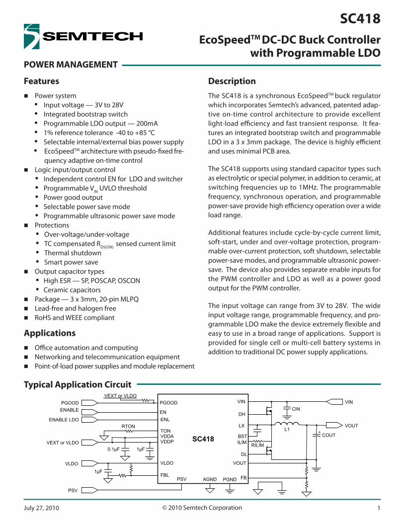
VOUT Voltage SelectionThe switcher output voltage is regulated by comparing VOUT as seen through a resistor divider at the FB pin to the internal 500mV reference voltage (see Figure 3).
R1
To FB pin
R2
VOUT
Figure 3 — Output Voltage Selection
Note that this control method regulates the valley of the output ripple voltage, not the DC value. The DC value of VOUT is offset by the output ripple according to the follow-ing equation.
2V
RR15.0V RIPPLE
2
1OUT
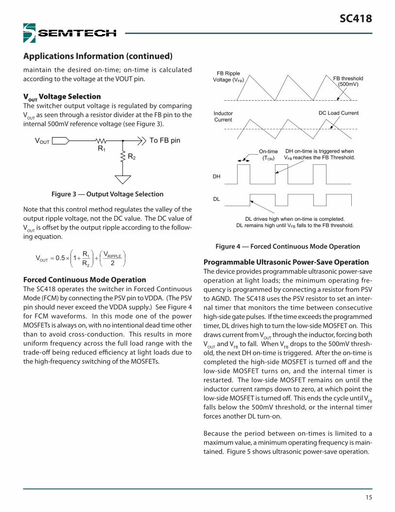
Forced Continuous Mode OperationThe SC418 operates the switcher in Forced Continuous Mode (FCM) by connecting the PSV pin to VDDA. (The PSV pin should never exceed the VDDA supply.) See Figure 4 for FCM waveforms. In this mode one of the power MOSFETs is always on, with no intentional dead time other than to avoid cross-conduction. This results in more uniform frequency across the full load range with the trade-off being reduced efficiency at light loads due to the high-frequency switching of the MOSFETs.
FB Ripple Voltage (VFB) FB threshold
DL
DH
Inductor Current
DC Load Current
DH on-time is triggered when VFB reaches the FB Threshold.
(500mV)
On-time (TON)
DL drives high when on-time is completed. DL remains high until VFB falls to the FB threshold.
Figure 4 — Forced Continuous Mode Operation
Programmable Ultrasonic Power-Save Operation The device provides programmable ultrasonic power-save operation at light loads; the minimum operating fre-quency is programmed by connecting a resistor from PSV to AGND. The SC418 uses the PSV resistor to set an inter-nal timer that monitors the time between consecutive high-side gate pulses. If the time exceeds the programmed timer, DL drives high to turn the low-side MOSFET on. This draws current from VOUT through the inductor, forcing both VOUT and VFB to fall. When VFB drops to the 500mV thresh-old, the next DH on-time is triggered. After the on-time is completed the high-side MOSFET is turned off and the low-side MOSFET turns on, and the internal timer is restarted. The low-side MOSFET remains on until the inductor current ramps down to zero, at which point the low-side MOSFET is turned off. This ends the cycle until VFB falls below the 500mV threshold, or the internal timer forces another DL turn-on.
Because the period between on-times is limited to a maximum value, a minimum operating frequency is main-tained. Figure 5 shows ultrasonic power-save operation.
Applications Information (continued)

SC418
16
FB Ripple Voltage (VFB)
FB threshold(500mV)
Inductor Current
DH
DL
(0A)
minimum frequency
After the programmable time-out, DL drives high if VFB has not reached the FB threshold.
DH On-time is triggered when VFB reaches the FB Threshold
On-time (TON)
programmable time-out
Figure 5 — Ultrasonic Power-Save Operation
The equation for determining the RPSV resistor value is shown next. The desired minimum frequency is fSWMIN.
SWMINPSV fpF350
1R
Note: the Power-save and Ultrasonic Power-save features are not supported for VDDA less than 4.5V.
Power-Save Mode OperationThe device provides power-save operation at light loads with no minimum operating frequency, selected by float-ing the PSV pin (no connection). In this mode of opera-tion, the zero cross comparator monitors inductor current via the voltage across the low-side MOSFET during the off-time. If the inductor current falls to zero for 8 consecu-tive switching cycles, the controller enters power-save operation. It will then turn off the low-side MOSFET on each subsequent cycle, provided that the current crosses zero. After the low-side MOSFET is off, both high-side and low-sides MOSFETs remain off until VFB drops to the 500mV threshold. While the MOSFETs are off the load is supplied by the output capacitor. If the inductor current does not reach zero on any switching cycle, the controller immedi-ately exits power-save and returns to forced continuous
mode. Figure 6 shows power-save operation at light loads. Note: the Power-save and Ultrasonic Power-save features are not supported for VDDA less than 4.5V.
FB Ripple Voltage
(VFB) FB threshold
DL
DH
Inductor Current
Zero (0A)
DH On-time is triggered when VFB reaches the FB Threshold.
(500mV)
On-time (TON)
DL drives high when on-time is completed. DL remains high until inductor current reaches zero.
Dead time varies according to load
Figure 6 — Power-Save Operation
Smart Power-Save ProtectionActive loads may leak current from a higher voltage into the switcher output. Under light load conditions with power-save enabled, this can force VOUT to slowly rise and reach the over-voltage threshold, resulting in a hard shut-down. Smart power-save prevents this condition. When the FB voltage exceeds 10% above nominal (exceeds 550mV), the device immediately disables power-save and DL drives high to turn on the low-side MOSFET. This draws current from VOUT through the inductor and causes VOUT to fall. When VFB drops back to the 500mV trip point, a normal TON switching cycle begins. This method prevents a hard OVP shutdown and cycles energy from VOUT back to VIN. It also minimizes operating power by avoiding forced con-duction mode operation. Figure 7 shows typical wave-forms for the Smart Power-save feature.
Applications Information (continued)
SC418
17
FB threshold
High-side Drive (DH)
Low-sideDrive (DL)
VOUT drifts up to due to leakage current flowing into COUT
DH and DL off
DL turns on when Smart PSAVE threshold is reached
Smart Power Save Threshold (550mV)
DL turns off when FB threshold is reached
Single DH on-time pulse after DL turn-off
VOUT discharges via inductor and low-side MOSFET
Normal DL pulse after DH on-time pulse
Normal VOUT ripple
Figure 7 — Smart Power-Save
SmartDriveTM
For each DH pulse, the DH driver initially turns on the high-side MOSFET at a slower speed, allowing a softer, smooth turn-off of the low-side diode. Once the diode is off and the LX voltage has risen 0.5V above PGND, the SmartDrive circuit automatically drives the high-side MOSFET on at a rapid rate. This technique reduces switch-ing noise while maintaining high efficiency, reducing the need for snubbers or series resistors in the gate drive.
Enable Input for Switching RegulatorThe EN input is a logic level input. When EN is low (grounded), the switching regulator is off and in its lowest power state. When EN is low and VDDA is above the VDDA UVLO threshold, the output of the switching regulator soft-discharges into the VOUT pin through an internal 15Ω resistor. When EN is a logic high (>1V) the switching regulator is enabled.
The EN input has internal resistors — 2MΩ pullup to VDDA, and a 1MΩ pulldown to AGND. These resistors will normally cause the EN voltage to be near the logic high trip point as VDDA reaches the VDDA UVLO threshold. To prevent undesired toggling of EN and erratic startup performance, the EN pin should not be allowed to float as open-circuit.
Note that the LDO enable pin (ENL) can also disable the switching regulator through the VIN UVLO function. Refer to the ENL Pin and VIN UVLO section.
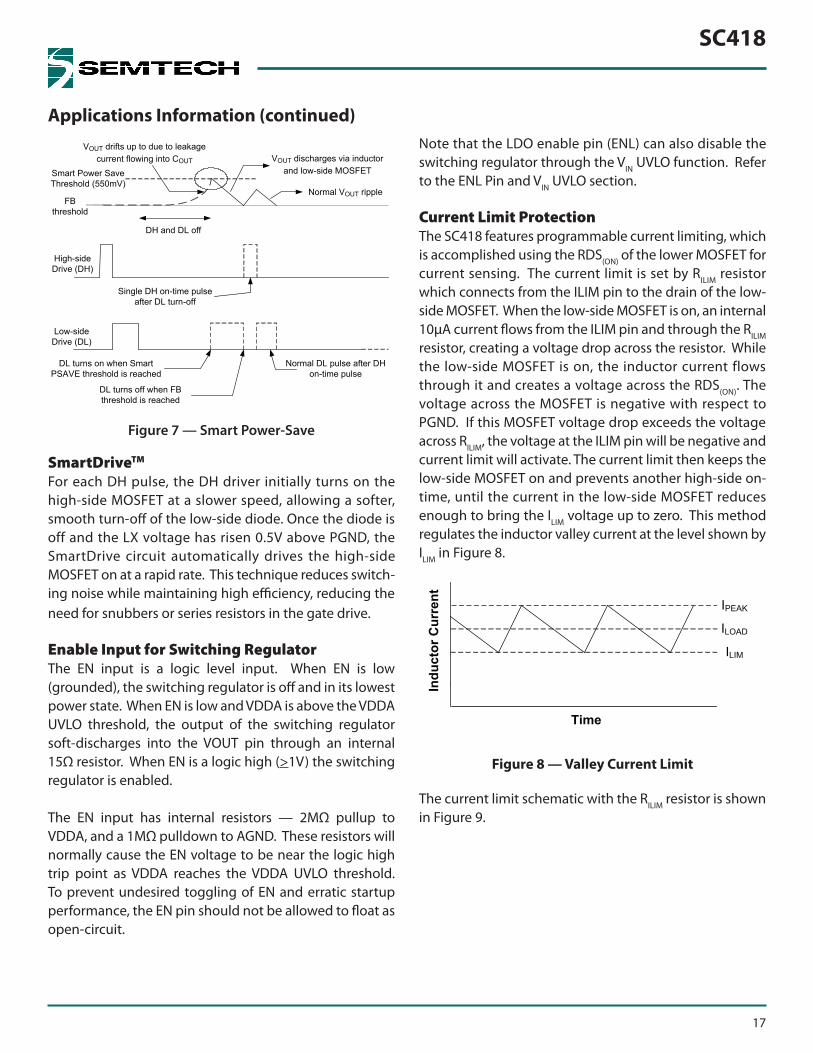
Current Limit ProtectionThe SC418 features programmable current limiting, which is accomplished using the RDS(ON) of the lower MOSFET for current sensing. The current limit is set by RILIM resistor which connects from the ILIM pin to the drain of the low-side MOSFET. When the low-side MOSFET is on, an internal 10μA current flows from the ILIM pin and through the RILIM resistor, creating a voltage drop across the resistor. While the low-side MOSFET is on, the inductor current flows through it and creates a voltage across the RDS(ON). The voltage across the MOSFET is negative with respect to PGND. If this MOSFET voltage drop exceeds the voltage across RILIM, the voltage at the ILIM pin will be negative and current limit will activate. The current limit then keeps the low-side MOSFET on and prevents another high-side on-time, until the current in the low-side MOSFET reduces enough to bring the ILIM voltage up to zero. This method regulates the inductor valley current at the level shown by ILIM in Figure 8.
Time
IPEAK
ILOAD
ILIM
Indu
ctor
Cur
rent
Figure 8 — Valley Current Limit
The current limit schematic with the RILIM resistor is shown in Figure 9.
Applications Information (continued)

SC418
18
VOUT
VIN
+CIN
Q2+D2
RILIM
CBST
Q1
L
PGNDDL
ILIMLXDH
BST
COUT
Figure 9 — Valley Current Limit
Setting the valley current limit to 10A results in a peak inductor current of 10A plus peak ripple current. In this situation the average current through the inductor is 10A plus one-half the peak-to-peak ripple current.
The RILIM value is calculated by the next equation.
A10IRR LIMDSON
ILIM
The internal 10μA current source is temperature compen-sated at 4100ppm in order to provide tracking with the RDSON.
Note that MOSFET RDS(ON) increases significantly if the VDDP voltage is 3.3V compared to 5.0V. When selecting the RILIM value, use the RDS(ON) value that corresponds to the VDDP voltage used in the application.
Soft-Start of PWM RegulatorSoft-start is achieved in the PWM regulator by using an internal voltage ramp as the reference for the FB compara-tor. The voltage ramp is generated using an internal charge pump which drives the reference from zero to 500mV in 1.2mV increments, using an internal 500kHz oscillator. When the ramp voltage reaches 500mV, the ramp is ignored and the FB comparator switches over to a fixed 500mV threshold. During soft-start the output voltage tracks the internal ramp, which limits the start-up inrush current and provides a controlled soft-start profile. Typical soft-start ramp time is 850μs.
During soft-start the regulator turns off the low-side MOSFET on any cycle if the inductor current falls to zero, regardless of the psave setting. This prevents negative inductor current, allowing the device to start into a pre-biased output.
Power Good OutputThe PGOOD (power good) output is an open-drain output which requires a pull-up resistor. When the voltage at the FB pin is 10% below the nominal voltage, PGOOD is pulled low. It remains low until the FB voltage returns above -8% of nominal. During start-up PGOOD is held low and will not be allowed to transition high until the PGOOD start-up delay fime has passed and soft-start is completed (when VFB reaches 500mV). The delay time starting from EN going high is typically 2ms for VDDA = 5V and 1ms for VDDA = 3.3V.
PGOOD will transition low if the FB voltage exceeds +20% of nominal (600mV), which is also the over-voltage shut-down threshold. PGOOD also pulls low if the EN pin is low when VDDA is present.
Output Over-Voltage ProtectionOVP (Over-voltage protection) becomes active as soon as the device is enabled. The OVP threshold is set at 500mV + 20% (600mV). When VFB exceeds the OVP threshold, DL latches high and the low-side MOSFET is turned on. DL remains high and the controller remains off until the EN input is toggled or VDDA is cycled. There is a 5μs delay built into the OVP detector to prevent false transitions. PGOOD is also low after an OVP event.
Output Under-Voltage ProtectionWhen VFB falls 25% below its nominal voltage (falls to 375mV) for eight consecutive clock cycles, the switcher is shut off and the DH and DL drives are pulled low to tri-state the MOSFETs. The controller stays off until EN is toggled or VDDA is cycled.
VDDA UVLO and PORThe VDDA Under-Voltage Lock-Out (UVLO) circuitry inhib-its switching and tri-states the DH/DL drivers until VDDA rises above 2.9V. When VDDA exceeds 2.9V, an internal POR (Power-On Reset) resets the fault latch and the soft-start counter and then the SC418 begins the soft-start
Applications Information (continued)
SC418
19
cycle. The switcher will shut off if VDDA falls below 2.7V. VDDP does not have ULVO protection.
Note that the VDDA UVLO will not stop MOSFET switching until the VDDA voltage falls to 2.7V. During this time the gate driver voltages will track the VDDA supply. Not all MOSFETs will operate or switch effectively at drive levels of 2.7V. For this reason, it is not recommended to rely on VDDA UVLO to shutdown the switcher unless the MOSFETs are capable of operating with 2.7V drive.
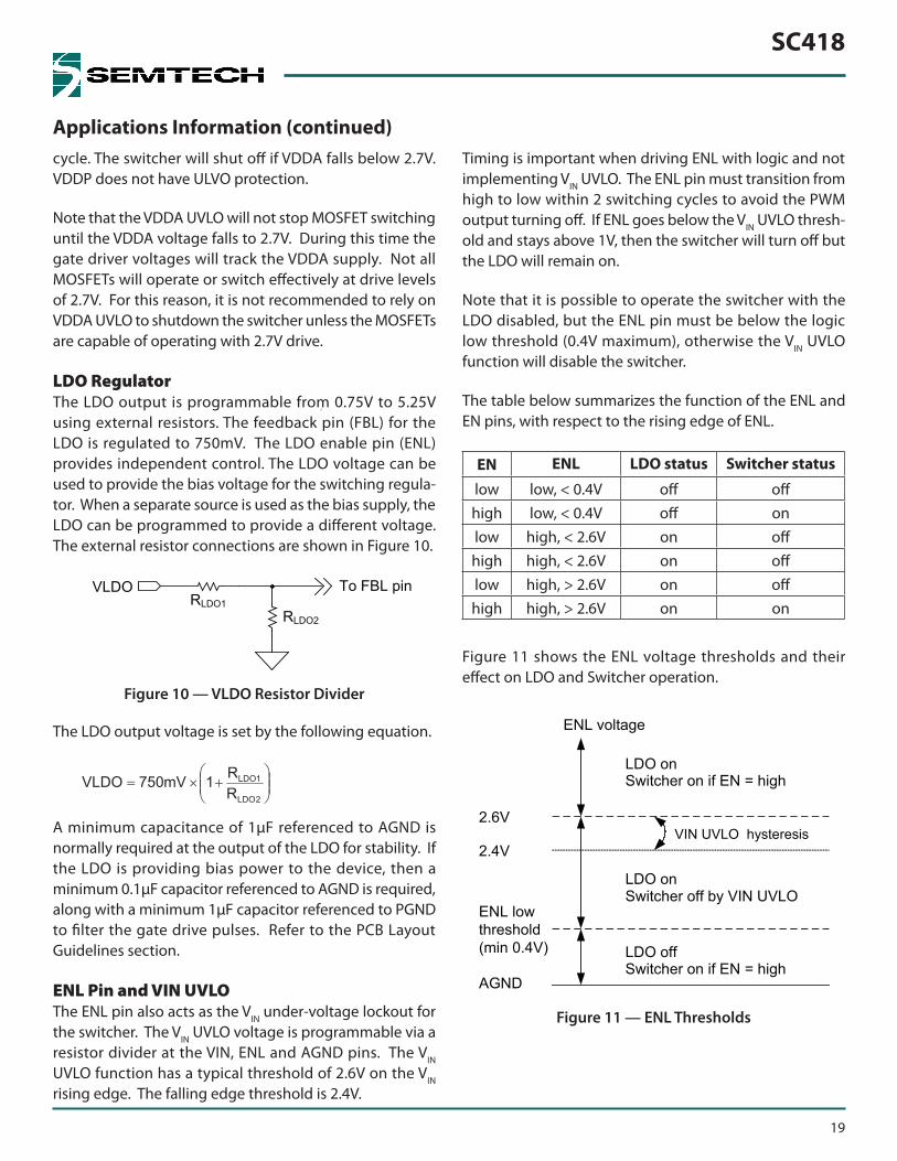
LDO RegulatorThe LDO output is programmable from 0.75V to 5.25V using external resistors. The feedback pin (FBL) for the LDO is regulated to 750mV. The LDO enable pin (ENL) provides independent control. The LDO voltage can be used to provide the bias voltage for the switching regula-tor. When a separate source is used as the bias supply, the LDO can be programmed to provide a different voltage. The external resistor connections are shown in Figure 10.
VLDO To FBL pin
RLDO2
RLDO1
Figure 10 — VLDO Resistor Divider
The LDO output voltage is set by the following equation.
2LDO
1LDO
RR1mV750VLDO
A minimum capacitance of 1μF referenced to AGND is normally required at the output of the LDO for stability. If the LDO is providing bias power to the device, then a minimum 0.1μF capacitor referenced to AGND is required, along with a minimum 1μF capacitor referenced to PGND to filter the gate drive pulses. Refer to the PCB Layout Guidelines section.
ENL Pin and VIN UVLOThe ENL pin also acts as the VIN under-voltage lockout for the switcher. The VIN UVLO voltage is programmable via a resistor divider at the VIN, ENL and AGND pins. The VIN UVLO function has a typical threshold of 2.6V on the VIN
rising edge. The falling edge threshold is 2.4V.
Timing is important when driving ENL with logic and not implementing VIN UVLO. The ENL pin must transition from high to low within 2 switching cycles to avoid the PWM output turning off. If ENL goes below the VIN UVLO thresh-old and stays above 1V, then the switcher will turn off but the LDO will remain on.
Note that it is possible to operate the switcher with the LDO disabled, but the ENL pin must be below the logic low threshold (0.4V maximum), otherwise the VIN UVLO function will disable the switcher.
The table below summarizes the function of the ENL and EN pins, with respect to the rising edge of ENL.
EN ENL LDO status Switcher status
low low, < 0.4V off offhigh low, < 0.4V off onlow high, < 2.6V on offhigh high, < 2.6V on offlow high, > 2.6V on offhigh high, > 2.6V on on
Figure 11 shows the ENL voltage thresholds and their effect on LDO and Switcher operation.
AGND
ENL low threshold (min 0.4V)
2.6V
2.4V
LDO on
LDO on
LDO off
VIN UVLO hysteresis
ENL voltage
Switcher on if EN = high
Switcher on if EN = high
Switcher off by VIN UVLO
Figure 11 — ENL Thresholds
Applications Information (continued)

SC418
20
Applications Information (continued)ENL Logic Control of PWM Operation When the ENL input exceeds the VIN UVLO threshold of 2.6V, internal logic checks the PGOOD signal. If PGOOD is high, the switcher is already running and the LDO will start without affecting the switcher. If PGOOD is low, the device disables PWM switching until the LDO output has reached 90% of its final value. This delay prevents the additional current needed by the DH and DL gate drives from over-loading the LDO at start-up.
In some cases it is desirable to use the VIN UVLO feature for the switcher without using the LDO. This can be done by connecting the FBL pin directly to VDDA. This disables the LDO, allowing the ENL pin to be used only for VIN UVLO for the switcher.
LDO Start-upBefore LDO start-up, the device checks the status of the following signals to ensure proper operation can be maintained.
ENL pinVLDO outputVIN input voltage
When the ENL pin is high and VIN is available, the LDO will begin start-up. During the initial phase, when VLDO is near zero, the LDO initiates a current-limited start-up (typically 115mA) to charge the output capacitor. When VLDO has reached 90% of the final value (as sensed at the FBL pin), the LDO current limit is increased to 200mA and the LDO output is quickly driven to the nominal value. The LDO start-up is shown in Figure 12.
VVLDO Final
90% of VVLDO Final
Constant current startup
Voltage regulating with ~200mA current limit
Figure 12 — LDO Start-Up
1.2.3.
LDO Switch-Over OperationThe SC418 includes a switch-over function for the LDO. The switch-over function is designed to increase efficiency by using the more efficient DC-DC converter to power the LDO output, avoiding the less efficient LDO regulator when possible. The switch-over function connects the VLDO pin directly to the VOUT pin through an internal switch. When the switch-over is complete the LDO is turned off, which reduces operating power loss. If the LDO output is used to bias the SC418, then after switch-over the device is self-powered from the switching regulator with the LDO turned off.
After the switcher completes soft-start, the switch-over logic waits for 32 switching cycles before it starts the switch-over. There are two methods of completing the switch-over of VLDO to VOUT.
In the first method, the LDO is already in regulation when the DC-DC converter is enabled. As soon as the PGOOD output goes high, the 32 cycle count is started. The volt-ages at the VLDO and VOUT pins are then compared; if the two voltages are within ±300mV of each other, the VLDO pin connects to the VOUT pin using an internal switch, and the LDO is turned off.
In the second method, the DC-DC converter is already running and the LDO is enabled. In this case the 32 cycle count is started as soon as the LDO reaches 90% of its final value. At this time, the VLDO and VOUT pins are compared, and if within ±300mV the switch-over occurs and the LDO is turned off.
Switch-over Limitations on VOUT and VLDOBecause the internal switch-over circuit always compares the VOUT and VLDO pins at start-up, there are limitations on permissible combinations of VOUT and VLDO. Consider the case where VOUT is programmed to 1.5V and VLDO is programmed to 1.8V. After start-up, the device would connect VOUT to VLDO and disable the LDO, since the two voltage are within the ±300mV switch-over window. To avoid unwanted switch-over, the minimum difference between VOUT and VLDO should be ±500mV.

SC418
21
Applications Information (continued)It is not recommended to use the switch-over feature for an output voltage of 3.3V or less since this does not provide sufficient voltage for the gate-source drive to the internal p-channel switch-over MOSFET.
It is not recommended to use the switch-over feature in cases where the device is powered from 3.3V which is ini-tially derived from the LDO. If the switch-over was used, then the 3.3V switcher output would pass through the switch-over MOSFET to power the VDDA/VDDP pins. The RDS(ON) of the switch-over device, typically 2.2 ohms at 3.3V, will cause a voltage drop across the device. The VDDA/VDDP pins would be typically 200mV or more below the 3.3V rail, due to the IR drop caused by the VDDA/VDDP current. If this voltage drop becomes large enough, the VDDA voltage will drop near the VDDA UVLO threshold, causing the device to shutdown.
Switch-over MOSFET Parasitic DiodesThe switch-over MOSFET contains parasitic diodes that are inherent to its construction, as shown in Figure 13.
Switchover MOSFET
Parasitic diode Parasitic diode
VDDA
VLDO VOUT
Switchover control
Figure 13— Switch-over MOSFET Parasitic Diodes
It is important to prevent forward bias of these diodes. The following two conditions must be satisfied in order for the parasitic diodes to stay off.
VDDA > VLDO VDDA > VOUT
If either VLDO or VOUT is higher than VDDA, then the respec-tive diode will turn on and the SC418 operating current will then flow through this diode. This has the potential of damaging the device.
Note that if the VDDA supply is 3.3V then both the LDO and switching regulator outputs are limited to 3.3V maximum. Trying to obtain higher voltages such as 5V
••
will forward-bias one of the parasitic diodes and could damage the device.
Using the Internal LDO to Bias the SC418The following steps must be followed when using the internal LDO to bias the device.
Connect VDDA and VDDP to VLDO before enabling the LDO.Any external load on VLDO should not exceed 40mA until the LDO voltage has reached 90% of final value.
When the switch-over feature is used and the VDDA/VDDP power comes from VOUT, the EN and ENL inputs must be used carefully. Do not connect the EN pin directly to VDDA or another supply voltage. If this is done, driving the ENL pin low (to AGND) will turn off the LDO and the LDO switch-over MOSFET, but the switcher will continue oper-ating. VOUT will feed into the LDO output and the VDDA/VDDP supplies through the internal parasitic diode. This can potentially damage the device, and also prevents the switcher from shutting off until the VDDA supply drops below the VDDA UVLO threshold. For these applications a dedicated logic signal is required to drive EN low and disable the switcher. This signal can be combined with the ENL signal if needed.
Design ProcedureWhen designing a switch mode supply the input voltage range, load current, switching frequency, and inductor ripple current must be specified.
The maximum input voltage (VINMAX) is the highest speci-fied input voltage. The minimum input voltage ( VINMIN) is determined by the lowest input voltage after evaluating the voltage drops due to connectors, fuses, switches, and PCB traces.
The following parameters define the design.
Nominal output voltage (VOUT)Static or DC output toleranceTransient responseMaximum load current (IOUT)
There are two values of load current to evaluate — con-tinuous load current and peak load current. Continuous
•
•
••••

SC418
22
Applications Information (continued)load current relates to thermal stresses which drive the selection of the inductor and input capacitors. Peak load current determines instantaneous component stresses and filtering requirements such as inductor saturation, output capacitors, and design of the current limit circuit.
The following values are used in this design.
VIN = 12V + 10%VOUT = 1.05V + 4%fSW = 250kHzLoad = 10A maximum
Frequency Selection Selection of the switching frequency requires making a trade-off between the size and cost of the external filter components (inductor and output capacitor) and the power conversion efficiency.
The desired switching frequency is 250kHz.
A resistor, RTON is used to program the on-time (indirectly setting the frequency) using the following equation.
OUT
INONTON VpF25
V)ns10T(R
To select RTON, use the maximum value for VIN, and for TON use the value associated with maximum VIN.
SWINMAX
OUTON fV
VT
TON = 318 ns at 13.2VIN, 1.05VOUT, 250kHz
Substituting for RTON results in the following solution.
RTON = 154.9kΩ, use RTON = 154kΩ
Inductor Selection In order to determine the inductance, the ripple current must first be defined. Low inductor values result in smaller size but create higher ripple current which can reduce efficiency. Higher inductor values will reduce the ripple current/voltage and for a given DC resistance are more efficient. However, larger inductance translates directly into larger packages and higher cost. Cost, size, output ripple, and efficiency are all used in the selection process.
••••
The ripple current will also set the boundary for power-save operation. The switching will typically enter power-save mode when the load current decreases to 1/2 of the ripple current. For example, if ripple current is 4A then Power-save operation will typically start for loads less than 2A. If ripple current is set at 40% of maximum load current, then power-save will start for loads less than 20% of maximum current.
The inductor value is typically selected to provide a ripple current that is between 25% to 50% of the maximum load current. This provides an optimal trade-off between cost, efficiency, and transient performance.
During the DH on-time, voltage across the inductor is (VIN - VOUT). The following equation for determining induc-tance is shown.
RIPPLE
ONOUTIN
IT)VV(L
In this example the inductor ripple current is set equal to 50% of the maximum load current. Thus ripple current will be 50% x 10A or 5A.
To find the minimum inductance needed, use the VIN and TON values that correspond to VINMAX.
H77.0A5
ns318)05.12.13(L
A slightly larger value of 0.88µH is selected. This will decrease the maximum IRIPPLE to 4.4A.
Note that the inductor must be rated for the maximum DC load current plus 1/2 of the ripple current.
The ripple current under minimum VIN conditions is also checked using the following equations.
ns384ns10V
VRpF25TINMIN
OUTTONVINMIN_ON
LT)VV(I ONOUTIN
RIPPLE
A25.4H088
ns384)05.18.10(I VINMIN_RIPPLE

SC418
23
Applications Information (continued)Capacitor Selection The output capacitors are chosen based on required ESR and capacitance. The maximum ESR requirement is con-trolled by the output ripple requirement and the DC toler-ance. The output voltage has a DC value that is equal to the valley of the output ripple plus 1/2 of the peak-to-peak ripple. Change in the output ripple voltage will lead to a change in DC voltage at the output.
The design goal is for the output voltage regulation to be ±4% under static conditions. The internal 500mV refer-ence tolerance is 1%. Allowing 1% tolerance from the FB resistor divider, this allows 2% tolerance due to VOUT ripple. Since this 2% error comes from 1/2 of the ripple voltage, the allowable ripple is 4%, or 42mV for a 1.05V output.
The maximum ripple current of 4.4A creates a ripple voltage across the ESR. The maximum ESR value allowed is shown by the following equations.
A4.4mV42
IVESRRIPPLEMAX
RIPPLEMAX
ESRMAX = 9.5 mΩ
The output capacitance is chosen to meet transient requirements. A worst-case load release, from maximum load to no load at the exact moment when inductor current is at the peak, determines the required capaci-tance. If the load release is instantaneous (load changes from maximum to zero in < 1µs), the output capacitor must absorb all the inductor’s stored energy. This will cause a peak voltage on the capacitor according to the following equation.
2
OUT
2
PEAK
2
RIPPLEMAXOUT
MINVV
I21IL
COUT
Assuming a peak voltage VPEAK of 1.150 (100mV rise upon load release), and a 10A load release, the required capaci-tance is shown by the next equation.
22
2
MIN05.115.1
4.42110H88.0
COUT
COUTMIN = 595µF
If the load release is relatively slow, the output capacitance can be reduced. At heavy loads during normal switching, when the FB pin is above the 500mV reference, the DL output is high and the low-side MOSFET is on. During this time, the voltage across the inductor is approximately -VOUT. This causes a down-slope or falling di/dt in the inductor. If the load di/dt is not faster than the -di/dt in the inductor, then the inductor current will tend to track the falling load current. This will reduce the excess induc-tive energy that must be absorbed by the output capaci-tor, therefore a smaller capacitance can be used.
The following can be used to calculate the needed capaci-tance for a given dILOAD/dt. Peak inductor current is shown by the next equation.
ILPK = IMAX + 1/2 x IRIPPLEMAX
ILPK = 10 + 1/2 x 4.4 = 12.2A
dtdlCurrentLoadofchangeofRate LOAD
IMAX = maximum load release = 10A
OUTPK
LOAD
MAX
OUT
LPK
LPKOUTVV2
dtdlI
VIL
IC
Example
sA5.2
dtdlLOAD
This would cause the output current to move from 10A to zero in 4µs as shown by the following equation.
05.115.12
s15.2
1005.1
2.12H88.02.12COUT
COUT = 379µF
Note that COUT is much smaller in this example, 379µF compared to 595µF based on a worst-case load release. To

SC418
24
Applications Information (continued)meet the two design criteria of minimum 379µF and maximum 9mΩ ESR, select two capacitors rated at 220µF and 15mΩ ESR.
It is recommended that an additional small capacitor be placed in parallel with COUT in order to filter high frequency switching noise.
Stability ConsiderationsUnstable operation is possible with adaptive on-time con-trollers, and usually takes the form of double-pulsing or ESR loop instability.
Double-pulsing occurs due to switching noise seen at the FB input or because the FB ripple voltage is too low. This causes the FB comparator to trigger prematurely after the 250ns minimum off-time has expired. In extreme cases the noise can cause three or more successive on-times. Double-pulsing will result in higher ripple voltage at the output, but in most applications it will not affect opera-tion. This form of instability can usually be avoided by providing the FB pin with a smooth, clean ripple signal that is at least 10mVp-p, which may dictate the need to increase the ESR of the output capacitors. It is also impera-tive to provide a proper PCB layout as discussed in the Layout Guidelines section.
Another way to eliminate doubling-pulsing is to add a small capacitor across the upper feedback resistor, as shown in Figure 14. This capacitor should be left unpopu-lated unless it can be confirmed that double-pulsing exists. Adding the CTOP capacitor will couple more ripple into FB to help eliminate the problem. An optional con-nection on the PCB should be available for this capacitor.
VOUT To FB pin
R2
R1
CTOP
Figure 14 — Capacitor Coupling to FB Pin
ESR loop instability is caused by insufficient ESR. The details of this stability issue are discussed in the ESR Requirements section. The best method for checking sta-bility is to apply a zero-to-full load transient and observe the output voltage ripple envelope for overshoot and ringing. Ringing for more than one cycle after the initial step is an indication that the ESR should be increased.
One simple way to solve this problem is to add trace resis-tance in the high current output path. A side effect of adding trace resistance is decreased load regulation.
ESR RequirementsA minimum ESR is required for two reasons. One reason is to generate enough output ripple voltage to provide 10mVp-p at the FB pin (after the resistor divider) to avoid double-pulsing.
The second reason is to prevent instability due to insuffi-cient ESR. The on-time control regulates the valley of the output ripple voltage. This ripple voltage is the sum of the two voltages. One is the ripple generated by the ESR, the other is the ripple due to capacitive charging and dis-charging during the switching cycle. For most applica-tions the minimum ESR ripple voltage is dominated by the output capacitors, typically SP or POSCAP devices. For stability the ESR zero of the output capacitor should be lower than approximately one-third the switching fre-quency. The formula for minimum ESR is shown by the following equation.
swOUTMIN fC2
3SRE
Using Ceramic Output CapacitorsWhen applications use ceramic output capacitors, the ESR is normally too small to meet the previously stated ESR criteria. In these applications it is necessary to add a small virtual ESR network composed of two capacitors and one resistor, as shown in Figure 15.

SC418
25
Applications Information (continued)
R1
R2FB pin
CC COUT
L
Low-side
High-side CLRL
Figure 15 — Virtual ESR Ramp Current
This network creates a ramp voltage across CL, analogous to the ramp voltage generated across the ESR of a stan-dard capacitor. This ramp is then capacitively coupled into the FB pin via capacitor CC.
Dropout PerformanceThe output voltage adjust range for continuous-conduc-tion operation is limited by the fixed 250ns (typical) minimum off-time of the one-shot. When working with low input voltages, the duty-factor limit must be calcu-lated using worst-case values for on and off times.
The duty-factor limitation is shown by the following equation.
)MAX(OFF)MIN(ON
)MIN(ON
TTT
DUTY
The inductor resistance and MOSFET on-state voltage drops must be included when performing worst-case dropout duty-factor calculations.
System DC Accuracy (VOUT Controller)Three factors affect VOUT accuracy: the trip point of the FB error comparator, the ripple voltage variation with line and load, and the external resistor tolerance. The error comparator offset is trimmed so that under static condi-tions it trips when the feedback pin is 500mV, + 1%.
The on-time pulse from the SC418 in the design example is calculated to give a pseudo-fixed frequency of 250kHz. Some frequency variation with line and load is expected. This variation changes the output ripple voltage. Because adaptive on-time converters regulate to the valley of the output ripple, ½ of the output ripple appears as a DC regu-lation error. For example, if the output ripple is 50mV with VIN = 6 volts, then the measured DC output will be 25mV above the comparator trip point. If the ripple increases to 80mV with VIN = 25V, then the measured DC output will be 40mV above the comparator trip. The best way to mini-mize this effect is to minimize the output ripple.
To compensate for valley regulation, it may be desirable to use passive droop. Take the feedback directly from the output side of the inductor and place a small amount of trace resistance between the inductor and output capaci-tor. This trace resistance should be optimized so that at full load the output droops to near the lower regulation limit. Passive droop minimizes the required output capaci-tance because the voltage excursions due to load steps are reduced as seen at the load.
The use of 1% feedback resistors contributes up to 1% error. If tighter DC accuracy is required, 0.1% resistors should be used.
The output inductor value may change with current. This will change the output ripple and therefore will have a minor effect on the DC output voltage. The output ESR also affects the output ripple and thus has a minor effect on the DC output voltage.
Switching Frequency VariationsThe switching frequency will vary depending on line and load conditions. The line variations are a result of fixed propagation delays in the on-time one-shot, as well as unavoidable delays in the external MOSFET switching. As VIN increases, these factors make the actual DH on-time slightly longer than the ideal on-time. The net effect is that frequency tends to falls slightly with increasing input voltage.
The switching frequency also varies with load current as a result of the power losses in the MOSFETs and the induc-
SC418
26
Applications Information (continued)tor. For a conventional PWM constant-frequency con-verter, as load increases the duty cycle also increases slightly to compensate for IR and switching losses in the MOSFETs and inductor. A adaptive on-time converter must also compensate for the same losses by increasing the effective duty cycle (more time is spent drawing energy from VIN as losses increase). Because the on-time is essentially constant for a given VOUT/VIN combination, to offset the losses the off-time will reduce slightly as load increases. The net effect is that switching frequency increases slightly with increasing load.
PCB Layout Guidelines As with any switch-mode converter, good PCB layout is essential to achieving high performance. The following guidelines will provide an optimum PCB layout.
The device layout can be considered in four parts.
Grounding for PGND and AGNDPower components Low-noise analog circuitsBypass capacitors
Grounding for PGND and AGNDA ground plane layer for PGND is recommended to minimize the effects of switching noise, resis-tive losses, and to maximize heat removal from the power components. A separate ground plane or island should be used for AGND and all associated components. The AGND island should avoid overlapping switching signals on other layers (DH/DL/BST/LX).Connect PGND and AGND together with a zero ohm resistor or copper trace. Make the connec-tion near the AGND and PGND pins of the IC.
Power ComponentsUse short, wide connections between the power components.
Input capacitors and high-side MOSFETsHigh-side and Low-side MOSFETs and inductor (LX connection). Use wide copper traces to provide high current carrying capacity and for heat dissipation. Inductor and output capacitors.
••••
•
•
•
••
•
All PGND connections — the input capacitors, low-side MOSFETs, output capacitors, and the PGND pin of the SC418.
An inner layer ground plane is recom-mended. Each power component requires a short, low impedance connection to the PGND plane.Place vias to the PGND plane directly near the component pins.
Use short wide traces for the pin connections from the SC418 (LX, DH, DL and BST). Do not route these traces near the sensitive low-noise analog signals (FB, FBL, TON, VOUT).
Low-noise Analog CircuitsLow-noise analog circuits are sensitive circuits that are referenced to AGND. Due to their high impedance and sensitivity to noise, it is important that these circuits be kept away from the switching signals.
Use a plane or solid area for AGND. Place all components connected to AGND above this area.
Use short direct traces for the AGND con-nections to all components. Place vias to the AGND plane directly near the component pins.
Proper routing of the VOUT sense trace is essential since it feeds into the FB resistor divider. Noise on the FB waveform will cause instability and multiple pulsing.
Connect the VOUT sense trace directly to the output capacitor or a ceramic bypass capacitor. Route this trace over to the VOUT pin, carefully avoiding all switching signals and power components. Route this trace in a quiet layer if possible. Route this trace away from the switch-ing traces and components, even if the trace is longer. Avoid shorter trace routing through the power switching area.If a bypass capacitor is used at the IC side of the VOUT sense trace, it should be placed near the FB resistor divider.
•
•
•
•

SC418
27
Applications Information (continued)All components connected to the FB pin must be located near the pin. The FB traces should be kept small and not routed near any noisy switch-ing connections or power components.Place the RILIM resistor near the IC. For an accu-rate ILIM current sense connection, route the RILIM trace directly to the drain of the low-side MOSFET (LX). Use an inner routing layer if needed. Place the RTON resistor near the TON pin. Route RTON to the TON pin and to AGND using short traces and avoid all switching signals.For the LDO components
The FBL resistors should be placed near the FBL pin. The area of the FBL traces should be minimized, avoiding all switch-ing connections.
The top FBL resistor must route directly to the LDO output capacitor. The LDO load current should not flow through this trace.
Bypass CapacitorsThe device requires bypass capacitors for the following pins.
VDDA pin with respect to AGND. This 0.1μF minimum capacitor must be placed and routed close to the IC pins, on the same layer as the IC.VDDP with respect to PGND. This 1μF minimum capacitor must be placed and routed close to the IC pins and on the same layer as the IC.BST pin with respect to LX. This 0.1μF minimum capacitor must be placed near the IC, on either side of the PCB. Use short traces for the routing between the capacitor and the IC.VLDO pin with respect to AGND.
This is the LDO output capacitor.The placement of this capacitor is not critical, however for routing it is important that the top FBL resistor connects directly to this capacitor, and that the LDO load current does not flow through this trace.If VLDO is not used to power the device then a minimum 1μF capacitor referenced to AGND is required. If VLDO is used to power the device then
•
•
•
•
•
•
•
•
the VDDA and VDDP capacitors also function as the LDO output capacitor. For VDDA, a minimum 0.1μF capacitor ref-erenced to AGND is required. For VDDP, a minimum 1μF capacitor referenced to PGND is required.
VIN pin with respect to AGND. This 0.1μF minimum capacitor must be placed and routed close to the IC pins. This capacitor provides noise filtering for the input to the internal LDO.
•
SC418
28
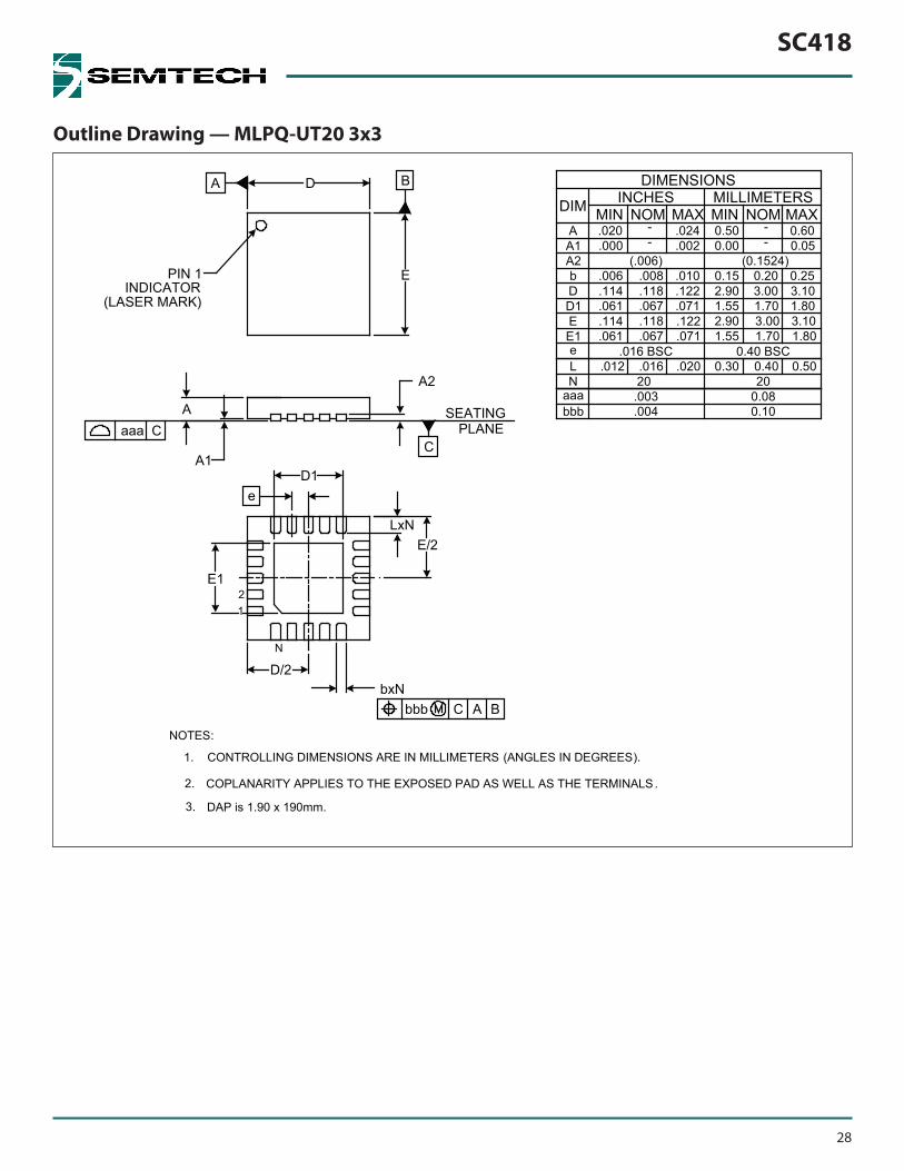
Outline Drawing — MLPQ-UT20 3x3
e
12
N
PIN 1INDICATOR
(LASER MARK)
A1
A
A2
C
SEATING PLANE
E/2
D/2
b .006 .008 .010 0.15 0.20 0.25
LxN
bxN
D1
E1
COPLANARITY APPLIES TO THE EXPOSED PAD AS WELL AS THE TERMINALS.2.
CONTROLLING DIMENSIONS ARE IN MILLIMETERS (ANGLES IN DEGREES).1.
INCHESDIMENSIONS
NOM
e
bbbaaa
A1A2
D1
E1
DIM
NL
E
MIN
D
A
MILLIMETERSMAXMINMAX NOM
E
BD
.114 .118 3.00.122 2.90 3.10
NOTES:
bbb C A B
aaa C
.003
.061
20
.067
.000
.020--
(.006)
0.0820
.071 1.55
.024
.002 0.000.50
1.801.70
0.050.60
(0.1524)--
.004 0.10
1.552.90
1.70 1.803.00 3.10
0.40 BSC.016 BSC0.30.012 .020.016 0.40 0.50
.122.118.114
.071.067.061
A
DAP is 1.90 x 190mm.3.

SC418
29
Land Pattern — MLPQ-UT20 3x3
THIS LAND PATTERN IS FOR REFERENCE PURPOSES ONLY.CONSULT YOUR MANUFACTURING GROUP TO ENSURE YOURCOMPANY'S MANUFACTURING GUIDELINES ARE MET.
NOTES:1.
C
Z
R
YX
G
P
H
.146
.004
.008
.031
.083
.067
.016
3.70
0.200.80
0.10
1.70
0.40
2.10
DIM(2.90)
MILLIMETERS
DIMENSIONS
(.114)INCHES
CONTROLLING DIMENSIONS ARE IN MILLIMETERS (ANGLES IN DEGREES).
2.
K .067 1.70
THERMAL VIAS IN THE LAND PATTERN OF THE EXPOSED PADSHALL BE CONNECTED TO A SYSTEM GROUND PLANE.
FUNCTIONAL PERFORMANCE OF THE DEVICE.FAILURE TO DO SO MAY COMPROMISE THE THERMAL AND/OR
3.
H
K
R
(C)
XP
Y
GZ

SC418
30
Contact Information
Semtech CorporationPower Management Products Division200 Flynn Road, Camarillo, CA 93012
Phone: (805) 498-2111 Fax: (805) 498-3804
www.semtech.com
© Semtech 2010
All rights reserved. Reproduction in whole or in part is prohibited without the prior written consent of the copyright owner. The information presented in this document does not form part of any quotation or contract, is believed to be accurate and reliable and may be changed without notice. No liability will be accepted by the publisher for any conse-quence of its use. Publication thereof does not convey nor imply any license under patent or other industrial or intellec-tual property rights. Semtech assumes no responsibility or liability whatsoever for any failure or unexpected operation resulting from misuse, neglect improper installation, repair or improper handling or unusual physical or electrical stress including, but not limited to, exposure to parameters beyond the specified maximum ratings or operation outside the specified range.
SEMTECH PRODUCTS ARE NOT DESIGNED, INTENDED, AUTHORIZED OR WARRANTED TO BE SUITABLE FOR USE IN LIFE-SUPPORT APPLICATIONS, DEVICES OR SYSTEMS OR OTHER CRITICAL APPLICATIONS. INCLUSION OF SEMTECH PRODUCTS IN SUCH APPLICATIONS IS UNDERSTOOD TO BE UNDERTAKEN SOLELY AT THE CUSTOMER’S OWN RISK. Should a customer purchase or use Semtech products for any such unauthorized application, the customer shall indemnify and hold Semtech and its officers, employees, subsidiaries, affiliates, and distributors harmless against all claims, costs damages and attorney fees which could arise.
Notice: All referenced brands, product names, service names and trademarks are the property of their respective owners.