rotman lens design_chrisp_ieee mw mag dec 2008
DESCRIPTION
expain how to use RLD software to design rotman lens design .TRANSCRIPT

138 December 2008
Since its invention in the early 1960s [1], the RotmanLens has proven itself to be a useful beamformer fordesigners of electronically scanned arrays. Inherent in
its design is a true time delay phase shift capability that isindependent of frequency and removes the need for costlyphase shifters to steer a beam over wide angles. The RotmanLens has a long history in military radar, but it has also beenused in communication systems.
Recently, the United States Army Research Laboratoryfunded a project to generate software for designing RotmanLenses as part of an initiative to develop low-cost electronicscanning arrays for communication systems operating fromC band (4–8 GHz) up to Ka Band (27.5–31 GHz) [2], [3]. Thebroadband performance of Rotman Lenses meets a key needof allowing the same antenna system to serve multiple func-tions, thus further reducing cost, complexity, and weight. Theproject focused on microstrip and stripline designs due totheir relative simplicity of construction compared to precisely-machined waveguides.
This article uses the developed software to design andanalyze a microstrip Rotman Lens for the Ku band. The ini-tial lens design will come from a tool based on geometricaloptics (GO). A second stage of analysis will be performedusing a full wave finite difference time domain (FDTD)solver. The results between the first-cut design tool and thecomprehensive FDTD solver will be compared, and some of
the design trades will be explored to gauge their impact onthe performance of the lens.
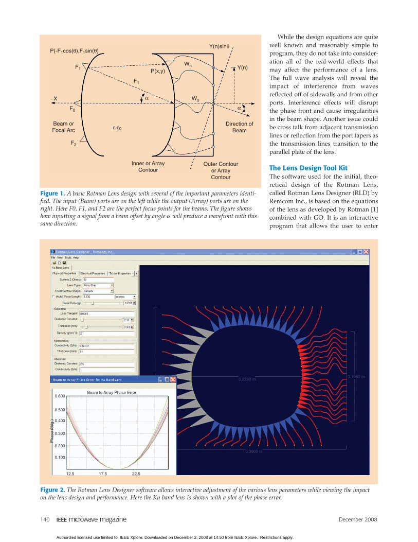
Rotman Lenses BrieflyA Rotman Lens is a parallel plate device used to feed anantenna array. It has a carefully chosen shape and appropri-ate length transmission lines to produce a wave front acrossthe output that is phased by the time delay in the signaltransmission. Each input port will produce a distinct beam,shifted in angle at the output, so sweeping the beam requiresfeeding a different port or feeding combinations of ports. Ageneral layout is shown in Figure 1, where the input (beam)ports are to the left and the output (array) ports are at theright. By design, there are three perfect focus beams withother beam ports surrounding them that have slightly lessthan perfect focus.
The design of the lens is controlled by a series of equa-tions that set the focal points and array positions. Theinputs during the design of the system can include thedesired scan angle of the array, the frequency and band-width of the lens, the number of beams and array ele-ments desired, and the spacing of those elements. Otherfactors in the design will include the fabrication tech-nique (typically microstrip, stripline, or waveguide) andrequired size. The lenses can be fairly large, on the orderof hundreds of square wavelengths, so high dielectricconstant substrates are often used to reduce the size and,in some cases, the weight of the lens. A single lens willtypically produce a fan beam, depending on the antennaarray used, so several lenses can be stacked to shape thebeam in a second direction.
Rotman Lens Design and Simulation in Software■ Christopher W. Penney
Christopher W. Penney ([email protected]) is with Remcom Inc., State College, Pennsylvania, USA.
Digital Object Identifier 10.1109/MMM.2008.929774
Authorized licensed use limited to: IEEE Xplore. Downloaded on December 2, 2008 at 14:50 from IEEE Xplore. Restrictions apply.
140 December 2008
While the design equations are quitewell known and reasonably simple toprogram, they do not take into consider-ation all of the real-world effects thatmay affect the performance of a lens.The full wave analysis will reveal theimpact of interference from wavesreflected off of sidewalls and from otherports. Interference effects will disruptthe phase front and cause irregularitiesin the beam shape. Another issue couldbe cross talk from adjacent transmissionlines or reflection from the port tapers asthe transmission lines transition to theparallel plate of the lens.
The Lens Design Tool KitThe software used for the initial, theo-retical design of the Rotman Lens,called Rotman Lens Designer (RLD) byRemcom Inc., is based on the equationsof the lens as developed by Rotman [1]combined with GO. It is an interactiveprogram that allows the user to enter
Figure 1. A basic Rotman Lens design with several of the important parameters identi-fied. The input (Beam) ports are on the left while the output (Array) ports are on theright. Here F0, F1, and F2 are the perfect focus points for the beams. The figure showshow inputting a signal from a beam offset by angle α will produce a wavefront with thissame direction.
P(-F1cos(θ),F1sin(θ)
F1
F1
Wn
Wo
Y(n)sinθ
Y(n)P(x,y)
F2
F0
Beam orFocal Arc
Inner or ArrayContour
Outer Contouror ArrayContour
Direction ofBeam
−X α
α
εrε0
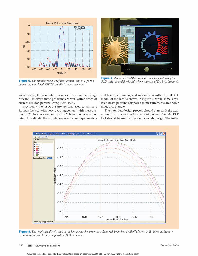
Figure 2. The Rotman Lens Designer software allows interactive adjustment of the various lens parameters while viewing the impacton the lens design and performance. Here the Ku band lens is shown with a plot of the phase error.
Beam to Array Phase Error
Pha
se (
deg.
) 0.400
0.500
0.600
0.300
0.200
0.100
12.5 17.5 22.5
0.3909 m
0.2360 m0.1960 m
Authorized licensed use limited to: IEEE Xplore. Downloaded on December 2, 2008 at 14:50 from IEEE Xplore. Restrictions apply.

December 2008 141
and modify a variety of parameters while viewing theimpact on the lens shape and performance. Output valuessuch as the phase error or array factor of the lens will updatein real time as the parameters are adjusted, while other val-ues such as S-parameters and insertion loss can be comput-ed once a lens shape is set. A screen shot of the software isshown in Figure 2, where an example lens is shown alongwith some of the menus and an output plot. The designprocess implemented in the software is based in large parton that developed by Hansen [4]. The software assumes thatparasitic coupling and transmission line and material dis-persion are negligible while dummy load effectiveness isideal. Effects included are the direct and singly reflected
rays propagating between ports and the impact of dielectriclosses. The port voltage standing wave ratio (VSWR) isapproximated as are the transmission line losses.
The full wave solver used is XFDTD v7.0 from RemcomInc. The initial design from the RLD program may beimported into XFDTD as a computer aided design (CAD)file as shown in Figure 3. The more rigorous FDTD simula-tion will take into account most of the factors approximatedby the simpler RLD software. An FDTD solver breaks thegeometry into many small samples and updates the electricand magnetic fields on the edges of these samples as a func-tion of time. The sample size must be one-tenth of a wave-length or less, so for geometries of many hundreds of square
Figure 4. Shown is the geometry of an X-band Rotman Lens sim-ulated with XFDTD and compared to measured results. Theresults were previously published in [5].
15
10
0
Figure 5. The array factor for the Rotman Lens of Figure 4 com-paring simulated XFDTD results to measurements.
0 MeasuredXFDTD
Beam 10 Antenna Pattern
dB
−10
−20
−30
−40
−50−80 −60 −40 −20 0
Angle (°)20 40 60 80
Figure 3. The initial design from RLD is imported into XFDTD as a CAD object and the project parameters are set. Here the beam andarray ports are labeled for reference. The white portions of the geometry are the metal while the red portion is the dielectric substrate.
Beams Array
+5+8
−5−8
0
Authorized licensed use limited to: IEEE Xplore. Downloaded on December 2, 2008 at 14:50 from IEEE Xplore. Restrictions apply.
142 December 2008
wavelengths, the computer resources needed are fairly sig-nificant. However, these problems are well within reach ofcurrent desktop personal computers (PCs).
Previously, the XFDTD software was used to simulateRotman Lenses with very good agreement with measure-ments [5]. In that case, an existing X-band lens was simu-lated to validate the simulation results for S-parameters
and beam patterns against measured results. The XFDTDmodel of the lens is shown in Figure 4, while some simu-lated beam patterns compared to measurements are shownin Figures 5 and 6.
The intended design process should start with the defi-nition of the desired performance of the lens, then the RLDtool should be used to develop a rough design. The initial
Figure 6. The impulse response of the Rotman Lens in Figure 4comparing simulated XFDTD results to measurements.
0 MeasuredXFDTD
Beam 10 Impulse ResponsedB
−10
−20
−30
−40
−50−80 −60 −40 −20 0
Angle (°)20 40 60 80
Figure 7. Shown is a 10-GHz Rotman Lens designed using theRLD software and fabricated (photo courtesy of Dr. Erik Lenzing).
Figure 8. The amplitude distribution of the lens across the array ports from each beam has a roll off of about 3 dB. Here the beam toarray coupling amplitude computed by RLD is shown.
Beam to Array Coupling Amplitude
−12.5
−16.0
12.5 15.0 17.5 20.0Array Port Number
22.5 25.0
−15.5
−15.0
−14.5
−14.0
−13.5
−13.0
Am
plitu
de (
dB)
Authorized licensed use limited to: IEEE Xplore. Downloaded on December 2, 2008 at 14:50 from IEEE Xplore. Restrictions apply.

December 2008 143
design can be tuned for best theoretical performance with-in RLD, and then the design can be exported for fabrica-tion or further analysis. The full wave XFDTD solver maythen be used to verify the RLD results and perform finetuning, as needed on the design. On its own, the RLDdesigner has been used to develop a C-band lens for theU.S. Army that was fabricated. The measured results forthe lens showed good agreement with those from the GO-based RLD software [3]. Also, an X-band lens with a cen-ter frequency of 10 GHz was designedusing RLD, and good results with fullwave simulations and measurementswere found [6]. Figure 7 shows boththe RLD model of the X-band lens onscreen and an actual fabricated lensconstructed from the RLD model.
An Example Lens Design
Geometrical Optics SolverTo demonstrate the software, a realisticexample lens will be designed andsimulated. The design parameters arebased on those used previously by theArmy Research Lab [2]. The lens willhave eleven beams and a scan angle of±25° at a center frequency of 16 GHzwith a 4 GHz bandwidth. There will be16 array ports suitable for a 16-elementantenna array, and the element spacingwill be 13 mm or about 0.7 wave-lengths.
With the above design parameters,some choices can be made for the otherparameters of the lens. We will chooseto make the lens as a microstrip with a50 � impedance transmission lines anda Duroid substrate of 0.5 mm thicknessand a dielectric value of 2.33. The lenswill have a circular curvature on thebeam port side and moderately round-ed sidewalls ending in a number ofdummy ports to absorb energy andreduce reflections. To obtain better per-formance, the beam and array ports willbe adjusted so that each tapered line ispointing toward the center of the lenson the opposite side rather than beingnormal to the lens surface. This is
described as port pointing and improves the response of theouter beams, as we will show later. As for the size and focallength of the lens, the width will be fixed at 236 mm, orabout 19.5 wavelengths. This size is chosen to match thewidth of the lens constructed in [2].
Once the main parameters are set, a lens is created that willrequire tuning to obtain the desired performance. Typically,the tuning involves viewing an output quantity such as thephase error across the array port or the array factor (beampattern) while adjusting the focal ratio of the lens. The focalratio is a factor that is related the curvature of the lens and, asthe name implies, focuses the lens. A poorly focused lens willproduce a messy beam pattern, while a properly focused lenswill yield a distinct beam. For the array factor, a set of sym-metrical beams, shifted in angle, with low side lobes isdesired. A final design with well-focused beams was reachedwith a focal ratio of 1.099.
Figure 9. Plotted is the S-parameter magnitude over the frequency range of the lens atarray port −1 with beam 0 active.
S-Parameter MagnitudeBeam 0 to Array −1
Frequency (GHz)
Mag
nitu
de (
dB)
14 15 16 17 18
RLD
XFDTD
−10
−11
−12−13
−14−15
−16−17
−18
−19
−20
Figure 10. The phase generated by the full wave FDTD solver at the array ports is lin-ear over the entire frequency range of the lens.
Phase at Array Ports from Beam 00
−500
−1,000
−1,500
−2,000
−2,500
−3,000
−3,50014 15 16
Frequency (GHz)
Array +8
Array +4
Array −1
Array −5
Pha
se (
°)
17 18
Since its invention in the early1960s, the Rotman Lens has provenitself to be a useful beamformer fordesigners of electronically scannedarrays.
Authorized licensed use limited to: IEEE Xplore. Downloaded on December 2, 2008 at 14:50 from IEEE Xplore. Restrictions apply.

144 December 2008
Forming good beams also produces low phase erroracross the array ports, and for this lens, the error is less thanone degree for every port. The lens is designed with anamplitude distribution that rolls off about 3 dB from the cen-ter of the array ports to the edges, as shown in Figure 8. Eachplot shows the distribution across the output from one of thebeam ports.
The sidewall curvature is arbitrarily set at a unitless valueof 0.75, which produces a slightly curved edge. Since thedummy ports are assumed to be ideal, there will be littlechange in the output plots generated by RLD between differ-ent sidewall curvature settings. The impact of the sidewallcurvature will have to be examined in more detail by the fullwave solver. The aperture width of the dummy ports ischosen to be about the same as that of the beam ports, giving16 dummy ports per sidewall. Again, the impact of the sidesand number of dummy ports will need to be examined withthe full wave solver later.
One other interesting parameter that can be varied is thetaper angle of the ports, which transition the transmission
lines to the lens. The angle of this taper region will affect theVSWR of the ports. A default setting of 11° is chosen for theinitial design, and later, the impact of this parameter will beexamined using the full wave solver.
Transmission lines are added to all ports with the most crit-ical ones being those attached to the array ports. The relativelengths of these lines are set by the design equations, and anyerror in those lengths will throw off the phasing. However, afixed length of line may be added to each and is typicallyneeded to be able to route the lines as needed to the antenna
array while maintaining good separationdistances between the lines. The RLDsoftware will construct the lines but doesnot include any effects of crosstalkbetween lines. So, some care must beused to avoid getting the lines very closetogether and simulation with the fullwave solver will be needed to ensurethere are no issues related to the lines.
Once the final design is reached, thelens can be exported as a CAD file for usein fabrication or for loading into anothersolver. In this case, the lens will be sent tothe FDTD solver for further analysis.
Full Wave SolverThe metal portion of the lens design istypically imported as a CAD file into theFDTD software. The dielectric substrateand the ports at the ends of each linemust be added. As the lines are designedwith 50 � impedance, the ports will eachcontain a voltage source with 50 �
source impedance as well. For the S-parameter analysis, one beam port at atime will be chosen as active. The inputsignal to the active port is a broadbandGaussian pulse, which will excite fre-quencies over the entire bandwidth ofthe lens. The results collected will betime-domain signals of voltage and cur-rent at each port, which are then trans-formed to the frequency domain to giveS-parameters, impedance, and otheroutput quantities.
A critical step in the FDTD analysisis the creation of the FDTD mesh. In
Figure 11. (a) The S-parameter magnitude across the array ports at the center frequencyof the lens shows a 3 dB taper from the center to the edges. (b) The phase across the arrayports is close to linear. The plots are at the center frequency of 16 GHz.
Magnitude Across Array PortsBeam 0 Active
Phase Across Array PortsBeam 0 Active
RLD
XFDTD
Array Port No.
(a)
(b)
Array Port No.
RLD
XFDTD
−8 −7 −6 −5 −4 −3 −2 −1 1 2 3 4 5 6 7 8
−8 −7 −6 −5 −4 −3 −2 −1 1 2 3 4 5 6 7 8
S-P
aram
eter
(dB
)
−11
−13
−15
−17
−19
−21
−23
−25
Pha
se (
°)
−45
−35
−25
−15
−5
5
15
25
35
45
While the design equations arequite well known and reasonablysimple to program, they do not takeinto consideration all of the real-world effects that may affect theperformance of a lens.
Authorized licensed use limited to: IEEE Xplore. Downloaded on December 2, 2008 at 14:50 from IEEE Xplore. Restrictions apply.

December 2008 145
general, good results require that each transmission line isseveral cells across to give accurate sampling of the fields. Arecent advancement added to the XFDTD solver is a featurethat locates the edges of all geometry objects and adjusts themesh size local to that object to ensure that the object’s edgesare clearly defined by an FDTD cell edge. This feature isknown as fixed-point extraction, and it creates a precise meshwith nonuniform cell dimensions with minimal user inter-vention. The benefit of this approach is that it can save sig-nificant amounts of computer memory for most structuresand greatly simplifies the meshing process for the user. Forthe example lens created here, the meshcontains about 45 million cells with amaximum cell size of 0.5 mm and a min-imum cell size of 0.1 mm. The calcula-tion requires about 1.4 GB of memory tosolve. While these calculations would fiton a standard 32-b desktop PC, we willrun the simulations using a much fasterhardware minicluster, where a pair ofNVIDIA FX 5600 GPU cards has beenspecially programmed to simulate theFDTD equations. The simulations typi-cally require 40,000–60,000 steps in timeto reach convergence, and executiontimes on the hardware cluster are typi-cally between one and one-half and twohours. As the geometry structures aresymmetrical about the centerline, itwould have been possible to cut thegeometry in half and mirror it using anappropriate boundary condition. Thisapproach would save a significantamount of memory and cut the simula-tion time, but given the speed of thehardware platform, the setup time forthe user to create the mirrored geometrywould have negated the simulationtime savings. If the geometry structureof the Rotman Lens were so large thatthe FDTD mesh would not fit in memo-ry, this mirroring approach becomesessential to run the calculation.
ResultsAfter finishing the lens design and set-ting up and running a few simulationsfor several different beams, we can beginto compare results between the GOsolver and the full wave solver. We are
interested in several output quantities, including the S-para-meters at the array ports and the beam patterns generated bythe array. We will compare the S-parameter magnitude andphase, both as a function of frequency and as a function ofarray port, to ensure that the response matches our designgoals.
The most basic data that can be compared between thetwo programs is the array port S-parameters. Each array portwill have transmission S-parameter from each beam port thatvaries as a function of frequency. In Figure 9, we can see thatthe S-parameter magnitude results from the GO solver forthe center beam are linear and nearly constant with frequen-cy. The full wave solver results are based on the voltage andcurrent values received at the array port. They are clearlymore complex but still fairly constant across the frequencyrange showing good transmission for any frequency. There isan offset in the results where the GO results are several dBlower than the full wave solution caused by the worst-case
Figure 12. (a) For beam −3 active the magnitude across the array ports (top) showssome variation in the full wave solution that is not present in the geometrical optics solu-tion. In part the variations could be from sidewall reflections. (b) The phase shift acrossthe array ports is very close to linear.
Magnitude Across Array PortsBeam −3 Active
Phase Across Array PortsBeam −3 Active
RLD
XFDTD
Array Port No.
(a)
(b)
Array Port No.
Pha
se (
°)S
-Par
amet
er (
dB)
RLD
XFDTD
−11
−13
−15
−17
−19
−21
−23
−25
600.00
400.00
200.00
−200.00
−400.00
−600.00
0.00
1 2 3 4 5 6 7 8 9 10 11 12 13 14 15 16
1 2 3 4 5 6 7 8 9 10 11 12 13 14 15 16
In addition to constant magnituderesponse versus frequency, it isdesirable to have linear phaseresponse with frequency as well.
Authorized licensed use limited to: IEEE Xplore. Downloaded on December 2, 2008 at 14:50 from IEEE Xplore. Restrictions apply.

assumptions made in the RLD softwareabout the losses in the lens. Results forother beam and array combinations aresimilar.
In addition to constant magnituderesponse versus frequency, it is desir-able to have linear phase response withfrequency as well. In Figure 10, thephase of the S-parameter is plotted andwe can see that for several array ports,the phase shift as a function of frequen-cy from the full wave solver is quite lin-ear. Note that the phase response wasunrolled to give a linear plot ratherthan a saw-tooth pattern that wouldcome out by default. The results forother beam and array ports and fromthe GO solver are similar.
After comparing the frequencyresponse, we can look at the results atthe designed center frequency of thelens as a function of array port. Theseresults are obtained by extracting themagnitude and phase data at the cen-ter frequency from the frequency-domain S-parameter data generated bythe software. This process is handledby user-generated scripts that are sup-ported within the software for dataprocessing.
First, the center frequency S-parame-ter magnitude across the array ports forbeam 0 (center port) active are com-pared. Our design called for a 3 dB roll-off of the magnitude toward the ends ofthe array, and this does appear to be the
Figure 13. The array factor for the lens shows a strong central beam and very closeagreement is found between the geometrical optics and full wave solutions. The top plotis for the center beam while the lower plot is for one of the offset beams.
Array Factor for Beam 0A
rray
Fac
tor
Arr
ay F
acto
r
RLD
XFDTD
RLD
XFDTD
Array Factor for Beam −3
0
0
−5
−10
−15
−20
−25
−30
−35
−5
−10
−15
−20
−25
−30
−35−100 −50 0 50 100
−100 −50 0 50 100Degrees
Degrees
Figure 14. The current propagating across the lens fromthe −5 port (lowest left) shows the wave front will hitmany of the dummy ports with similar amplitude levels asthe array ports.
Figure 15. Several variations were made to the lens sidewalls,including (a) and (b) decreasing and increasing the curvature and(c) and (d) changing the size and number of dummy ports.
0.2360m 0.2360m
0.2360m0.2360m
(a) (b)
(d)(c)
146 December 2008
Authorized licensed use limited to: IEEE Xplore. Downloaded on December 2, 2008 at 14:50 from IEEE Xplore. Restrictions apply.
December 2008 147
case as shown in Figure 11(a). Again theGO results are lower due to higher loss-es assumed, but the shape of the plotsshows decent roll-off. For beam 0, thephase response [Figure 11(b)] should beflat across the array ports since each isabout the same distance from the centerbeam port. The results indicate thiswithin about ±5° of variation. Similarly,for beam −3 (see Figure 3 for beam loca-tions), the magnitude response acrossthe array ports shows the desired roll-off, although in the full wave results,there are some discontinuities in thecurve at the outer array ports (seeFigure 12). The phase response for beam−3 is quite linear across the array andthere is high correlation between theGO and full wave results.
During the design process, the shapeof the array factor was used to tune thelens. The array factor is computed asthe pattern that would be generated bya linear array of elements at the outputport locations. The factor is extractedfrom the full wave solver data by takingthe Fourier transform of the time-domain port voltage at each outputport location and using the complexfrequency-domain voltages as thesources for the linear array. Again, thispostprocessing is handled by a user-generated script in the software, andthe magnitudes are normalized to thepeak value. For beam 0, the array factorcomparison between the GO and fullwave solvers are nearly identical, withonly slight variations in the side lobelevels. For beam −3, the array factorresults have more variation in the sidelobes, but the main beam and majorside lobes show very good agreement.The array factor plots for the two beamsare shown in Figure 13.
Based on these results, it appearsthe GO solver is providing a very gooddesign for the lens as the agreementwith the full wave solver is close.However, since the GO solver makes anumber of simplifying assumptions, itmight be interesting to try some varia-tions of the lens design to see theimpact on the results as compared tothe full wave solution. One seeminglymajor simplification is that only directand singly reflected rays are includedin the GO solution, and absorption by
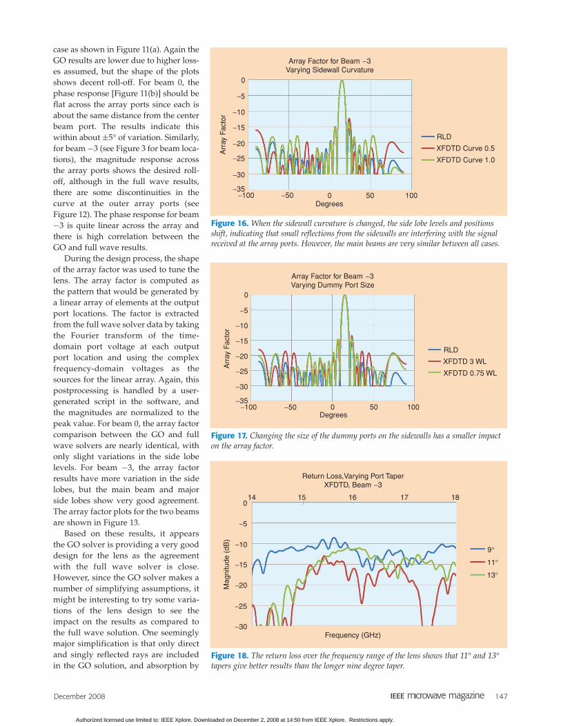
Figure 16. When the sidewall curvature is changed, the side lobe levels and positionsshift, indicating that small reflections from the sidewalls are interfering with the signalreceived at the array ports. However, the main beams are very similar between all cases.
−5
−10
−15
−20
−25
−30
−35−100 −50 0 50 100
Arr
ay F
acto
r
RLD
XFDTD Curve 0.5
XFDTD Curve 1.0
0
Array Factor for Beam −3Varying Sidewall Curvature
Degrees
Figure 17. Changing the size of the dummy ports on the sidewalls has a smaller impacton the array factor.
−5
−10
−15
−20
−25
−30
−35−100 −50 0 50 100
Arr
ay F
acto
r
RLD
XFDTD 3 WL
XFDTD 0.75 WL
0
Array Factor for Beam −3Varying Dummy Port Size
Degrees
Figure 18. The return loss over the frequency range of the lens shows that 11° and 13°tapers give better results than the longer nine degree taper.
Frequency (GHz)
9°
11°
13°
14 15 16 17 18
Return Loss,Varying Port TaperXFDTD, Beam −3
−5
−10
−15
−20
−25
−30
Mag
nitu
de (
dB)
0
Authorized licensed use limited to: IEEE Xplore. Downloaded on December 2, 2008 at 14:50 from IEEE Xplore. Restrictions apply.

148 December 2008
the dummy ports is considered to be ideal. In our previousresults, the center beam agreement was much betterbetween codes than the offset (beam −3) port. Certainly, theradiation from the lower beams will have much greaterinteraction with the sidewalls than the center beam. To showthis more clearly, the propagation of current on the lens sur-face from the lowest beam port (beam −5) is shown inFigure 14, and it is clear that a good portion of the highamplitude signal will hit the sidewall and go into thedummy terminals.
To gain a better perspective on the design choices, wewill vary both the curvature of the sidewalls and the sizeand number of dummy ports in our original lens designand compare results. First, the sidewall curvature will beincreased and decreased while keeping the dummy portaperture size fixed, as shown in Figure 15(a) and (b). This
causes the flatter sidewall case to lose one dummy port. Totest the impact of dummy port size, the sidewall curvaturewill remain the same while the dummy port aperture sizeis varied, as shown in Figure 15(c) and (d). The originaldummy port apertures were sized at 1.1 wavelengths inwidth, giving 15 ports on each sidewall. We’ll nowincrease the port size to 3 wavelengths to drop the numberper sidewall to six and decrease the port size to 0.75 wave-lengths to increase the number of ports per sidewall to 22.The GO results for all cases are virtually the same as theoriginal design since the sidewall changes have littleimpact on the equations used in that solver. The full waveresults show that the variations in the lens sidewall curva-ture shift the levels in the minor side lobes (Figure 16) thatare down more than 15 dB from the main beam. However,the main beam shape and position remain constant, so the
fields reflected from the sidewalls arefairly weak. Similarly, changing thedummy port sizes has some impact onthe side lobe levels, but no visibleimpact on the main beam (Figure 17).Changing the dummy port sizes hadvery little impact on the magnitude ofthe signal reaching the array ports forany of the beams simulated. This indi-cates that the sidewalls are not con-tributing strong reflections that aredisturbing beam patterns and littleenergy is lost to the dummy ports.
Another simplifying assumption ofthe GO solver relates to the calculationof losses and VSWR in the ports. Themost relevant characteristic of thedesign that relates to the port VSWR isthe shape of the transition regionbetween the transmission lines and the
Figure 19. (a) The lens has ports that are attached normal to the lens curve. This can result in beam ports that point toward the side-walls of the lens. (b) By turning on port pointing in the RLD software, each port is tilted so it is focused toward the center of the oppo-site side of the lens.
(a) (b)
Figure 20. With no port pointing used, the array factor for beam −3 degrades resultingin a poorly defined main beam with higher side lobes. In contrast, the lens with pointedports has a smoother beam (shown in Figure 13).
−5
−10
−15
−20
−25
−30
−35
Arr
ay F
acto
r
RLD No Pointing
XFDTD No Pointing
0
Array Factor for Beam −3
−100 −50 0 50 100Degrees
Authorized licensed use limited to: IEEE Xplore. Downloaded on December 2, 2008 at 14:50 from IEEE Xplore. Restrictions apply.

December 2008 149
lens. This shape is controlled by theport taper adjustment in the GO solver,which specifies an angle for the taper.The default design used a taper angle of11°, which gives a port length of about50 mm. We will adjust the port taperangle up and down to 13° and 9°, whichgives taper lengths of 40 and 60 mm,respectively. Here we will look at thereturn loss from the ports as a functionof frequency since that is the factor thatwill be most affected by the change. TheGO solver gives a constant return lossof about −12 dB for all the ports acrossthe entire frequency range. When thefull wave results are computed, theyshow significant variation in the returnloss (Figure 18). Although all results areacceptable, it appears the 11° and 13°taper angles give better return loss(lower reflection) across the frequencyrange than the 9° taper.
As a final investigation, let’s look into the matter of portpointing. With no port pointing, the beam and array portsare attached normally to the lens surface. In some cases,this can result in the outer beam ports pointing moretoward the sidewalls than toward the array ports. It hasbecome customary to attach the ports so they are pointedtoward the center of the opposite side of the lens. Examplesof each configuration are shown in Figure 19. It makessense that having the ports pointed toward the desiredlocation will result in better lens performance, and this iseasy to see in Figure 20, where the array factor for beam −3is plotted with no pointing. Previously, with port pointingapplied (Figure 13), this beam showed a clean array factorwith a well formed beam. Now with pointing turned off,the array factor is nonsymmetrical with higher side lobes.The agreement between the GO and full wave solvers ismuch lower here too as the fields propagated by the beamport will have much more interaction with the sidewalland dummy ports. This is a good indication that usingpointing will result in better lens performance and reducedlosses to the sidewalls.
A further question to ask related to pointing is whetherpointing the port toward the center of the opposite side of thelens will give the best performance for every situation. Toexperiment with this, the port angle for beam −3 with respectto the default pointing direction is parameterized in the fullwave solver (Figure 21), and the resulting array factors foreach case are compared. The middle position in Figure 21 isthe pointing position and rotations of ±5° and 10° are appliedto the port. Following the simulation, the results show thatincreasing the pointing angle by 5° for this beam in this lensdid give a very slightly more symmetrical beam pattern withlower side lobes. While the improvement is small in this exam-ple, it could be that for another lens, a more significantimprovement might be possible. However, the overall conclu-
sion is that the default pointing works quite well and is cer-tainly preferred over nonpointing ports.
ConclusionIn this article, two software tools for the design and simula-tion of Rotman Lenses were compared using a realistic exam-ple of a Ku-Band lens. The performance of the simpler, GOtool was found to be quite good compared to the more rigor-ous full wave solution. While the GO tool makes a number ofsimplifying assumptions, the results from several parametersweeps indicate that those assumptions are valid. For theexample studied here, the main area where the GO assump-tions affect the results, the reflections from the sidewalls, didnot significantly alter the beam patterns generated by thelens. In other lens designs, the impact of the simplifyingassumptions of the GO solver may be greater, so validationwith the full wave solver is certainly recommended. Overall,the two products provide a simple means to generate andfully analyze these complex devices.
References[1] W. Rotman and R. Turner, “Wide-angle microwave lens for line source
applications,” IEEE Trans. Antennas Propagat., vol. 11, no. 6, pp. 623–632,Nov. 1963.
[2] O. Kilic and S. Weiss, “Dielectric Rotman Lens design for multi-functionRF antenna applications,” in Proc. 2004 IEEE AP-S Int. Symp., June 2004,vol. 1, pp. 659–662.
[3] S. Weiss, S. Keller, and C. Ly, “Development of simple affordable beam-formers for army platforms,” presented at 2007 GOMACTech Conf., LakeBuena Vista, FL, Mar. 2007.
[4] R.C. Hansen, “Design trades for Rotman Lenses,” IEEE Trans. AntennasPropagat., vol. 39, no. 4, pp. 464–472, Apr. 1991.
[5] C.W. Penney, R.J. Luebbers, and E. Lenzing, “Broad band Rotman Lenssimulations in FDTD,” in Proc. 2005 IEEE AP-S Int. Symp., July 2005, vol.2B, pp. 51–54.
[6] S. Albarano III, E.H. Lenzing, C.W. Penney, and R.J. Luebbers, “Combinedanalytical-FDTD approach to Rotman Lens design,” presented at the 22thAnnual Review of Progress in Applied Computational Electromagnetics,Miami, FL, Mar. 2006.
Figure 21. Several shifted variations for the port at beam −3 are shown to demonstratethe range of values simulated. When performing the simulations, only one port at a timewas connected with the associated transmission line.
Authorized licensed use limited to: IEEE Xplore. Downloaded on December 2, 2008 at 14:50 from IEEE Xplore. Restrictions apply.