rockwell international thousand oaks-ca …ad-a113 007 rockwell international thousand oaks-ca...
TRANSCRIPT

AD-A113 007 ROCKWELL INTERNATIONAL THOUSAND OAKS-CA MICROELECTR-ETC F/6 2012GAAS SURFACE PASS! RATION FOR DEVICE APPLICATIONS UlDEC 81 R W GRANT. K R ELLIOTT, S P KOWALCZYK F33615-78-C-1891
UNCLASSIFIED ERC41OS1.41ITR AFWAL-TR-81-1209 NM.

wiliw11111I25 amLA111.III P R LU TE.4 CHART
MIRCP EOUINTS HR

AFWAL-TR-81-1209
GaAs SURFACE PASSIVATION FORO. DEVICE APPLICATIONS
R.W. Grant, K.R. Elliott, &P. Kowalczyk, D.L. Miller and4 J.R. Waldrop
Rockwell' International Microelectronics ResarcndDevelopment Center
~ 1049 Camino, Doe RiotThousand Oaks, CA 91360
December 1961
Interim Report for Period I April 1980 - 30 Septmber 1980
ip
- isv puW us dIbm umkwmid
DTICF1 LECTE !..
1 A -irUem PerL b s;a2 Jf04 am 089
LI8 0' O

I. -I
NOTICE
When Government drawings, specifications, or other data re used for any putPOsother than in connection with a definitely related Government procurement operation,the United Sttes Government thereby incurs no responsibility nor any obligation whatso-ever; and the fact that the government may have formulated, furnished, or in my waysupplied the soid dravings, specifications, or other data, is not to be regarded by implica-tion or otherwise i in any manner licensing the holder or any other person or corporation,or conveying any righlts or permission to manufacturejuse, or sell any patented inventionthat may in any way be related thereto.
This report has been reviewed by the Office of Public Affairs (ASD/PA) and isreleaseable to the National Technical Information Service (NTIS). At NTIS, it will beavailable to the general public, including foreign nations.
This technical report has been reviewed and is approved for publication.
DIETRICH W. LANGERProject EngineerElectronic Research BranchAvionics Laboratory
FOR THE COMMANDER
PHILIP 9. STOVER, ChiefElectronic Research BranchAvionics Laboratory
"If your addies has changed, if you wish to be removed from our mailing list, orif the addreuoe is no longer employed by your orgenization plem notify AFWAL/AADRW-PAFB, OH 45433 to help us maintain a current mailing list."
Copies of this report should not be returned ulss return is required by securitycsde on, ntractual obligations, or notice on a spef document

UNCLASSIFIEDIguRmTV CLASI"CATION OF TI46 PAG6 .1 Alme_
REPOT DOCUAUINTATiON PAGE n _ _ _ _MS__MC__s
I. EXPORT NUM89M . L ACCOIImON N& I I Nl's CATALOG NUmESP
AFWAL-TR-81-1209 1 '(4. TITLE (da OWO) S. TYPE OF REPORT & PEIOO COVERED
Interim Technical ReportGaAs SURFACE PASSIVATION FOR DEVICE for 1 Apr 80 - 30 Sep 80APPLICATIONS *. PERFORMING ORE. REPORT 14M0eR
ERC41051.41ITR7. AUTMO(s) 8. ONTRACT OW ANNUM 6 (s)
R.W. Grant, K.R. Elliott, S.P. Kowalczyk,D.L. Miller and J.R. Waldrop F33615-78-C-1591
9. PERFORMING ORGANIZATION NAME AND ADORESS I0. PNGlnAMO ELMNT. PNOJECr. TASK
Rockwell International UNIT NUNjIRS
Microelectronics Research & Development Center 61102F/2305R/R1/82P.O. Box 1085, Thousand Oaks, CA 91360
It. CONTROLLING OFFICE NAME AND AOORS 1l. REPORT DATE
Air Force Avionics Laboratory December 1981ATTN: AFWAL/AADR It I"VG-M OF PAGE
Wright Patterson AFB, OH 45433 6714L MONITORING AGENCY NAME 0 AUOR5WISSI dlMe fWIIIM COINMI OMC*) IL SECURITY CLASL (of hl. itw)
UNCLASSIFIED
IS. OC I.ICATION/OO, WRAINNG
I. DISTRIDJTION STATEMENT (ofWe Emvpf)
Approved for public release; distribution unlimited.
17. OISTRI8UTION STATEMENT (ol 0A" mb E In Wh 3. It dffomm IN RN= I
IL SUPPLE TARY NOTES
"i. g, woaoe RO note m W6V deg eas MqRMY OI EeIpr Wk mn*)
Gallium Arsenide Surface PassivationOxidation XPSGallium Aluminum Arsenide MBEInsulation
ML ASITACT (C10m 11e10O #"We I& mep o IN"000616 4114 ib.)
This document is the Interim Report #4 which covers the period 4/1/80through 9/30/80 for contract No. F33615-78-C-1591 entitled, "GaAs SurfacePassivation for Device Applications." C-V and I-V measurements are reportedfor several GaAs (100) MIS samples of both n- and p-type. The insulatorswere formed by thermal oxidation of MSE grown AllxGa As layers or byevaporation of S1Ox. A photochemical process was deve/oped to deposit S1O2on room temperature samples.
Powm
00 1 jAd1 3 M OITION OF I NV 6 ISGU .TE UNCLASSIFIEDSECUITV CLAINIICATIOW O Tis Prt (WGsm Wee Etwme)
" iml ii mm l i l II . .. . . . . . ll .. .. l ... .. . . .. . .. . . ... . .:. . .. .. . ... ../ L

TABLE OF CONTENTS
Section Pag
SUMMARY ....................... viIii
I. INTRODUCTION ................. . * .1.. . . .. * ...... . . 1II. SAMPLE PREPARATION..... ........... ...... .. ........... **.. 3
1. MBE Samples ............................. 3
2. Deposited Insulators. 73. XPS Study of Aluminum Oxide Growth ........................ 13
111 . SAMPLE ANALYSIS .................**......*......................... 18
1. C-V and I-V Measurements ........... ... 6 ....... ....... 18a. MBE amples ........ 0............................. 18b. Deposited Insulator Samples ........................... 28
2. Depth Profile of Sample No. 411 ........................... 37
IV. DISCUSSION OF PREVIOUS MBE RESULTS ............................. 42REFERENCES ....................... . . . . . . . ....... *........ 46
APPENDIX.*.*. *.. ...... . . . . . . . . . . . . . . . . ...... 48
Accesslon ForNTIS GRA&I
DTIC TABUnannounced ElJust if fea c-t
By
-Distribut ion/
._ Avatlbt litv CQ,:,:.,
Avatl.~I'Dist I -1
IrNII'CTED
iii

LIST OF ILLUSTRATIONS
Figure Page
1 Schematic illustration of structure for three MBE samples ...... 4
2 Idealized flat-band diagram constructed assuming that- 88% of energy gap discontinuity Is associated with theconduction-band edge (Ec) and - 12% with the valence bandedge (Ev)...................................................... 6
3 XPS spectrum of evaporated SiOx,................................ 10
4 XPS spectra in binding-energy region of Si 2p line for (top)SiOx material before evaporation (middle) SiOx after vacuumevaporation and (bottom) SiO x after evaporation in 02 withpresence of UV lgt...................... 11
5 XPS spectra in region of Al 2p line for (A) evaporationof Al in 02 with UV light present, and (B) oxidation ofAl film in (A) at - 510 0 C.................................... 14
6 XPS spectra in region of Al 2p line for (C) additional Alevaporated in 0 onto the surface characterized as spectrum(B) In Fig. 5 wfile this surface was at 520C and (D)oxidation of sample in (C) at - 520 0C.......................... 15
7 XPS spectra in region of Al 2p line. Spectrum labeled (D) isrepeated from Fig. 6 for reference. Spectrum (E) was obtainedafter deposition of Al onto the sample at room temperaturewhile in the presence of an 02 plasma discharge ................ 16
8 C-V measurements for Sample No. 491............................ 20
9 C-V measurements for Sample No. 490............................ 21
10 C-V measurements for Sample No. 493............................ 23
11 C-V measurements at 1 tHz for sample No. 411 after threesequential oxidations, (top) 0.5 min oxidation, (middle)10 min oxidation, and (bottom) 60 min oxidation ................ 24
12 C-V measurements at 1 MHz for same sample as in Fig. 11,(top) 330 min oxidation, (bottom) 1575 min oxidation ........... 26
13 C-V measurements at 1 MHz for same sample as in Figs. 11and 12 after 10,455 min oxidation............................. 27
Iv
LIST OF ILLUSTRATIONSI
Figure Page
14 C-V measurements at 1 MHz for sample X1 ........................ 29
15 I-V measurements for sample Xl (p-type) ........................ 31
16 Comparison of leakage currents for vacuum evaporatedSiOx and photochemically produced SiO 2 insulators .............. 32
17 C-V measurements at 1 MHz for sample X2 (p-type) ............... 33
18 C-V measurements at 1 MHz for sample X3 (p-type) ............... 34
19 C-V measurements at 1 MHz for sample X4 (n-type)............... 35
20 C-V measurements at 1 MHz for sample X5 (n-type) ............... 36
21 C-V measurements at 1 MHz for sample X3 (n-type).Data obtained by B. Bayraktaroglu (WPAFB)...................... 38
22 G-V measurements at 100 kHz for sample X3 (n-type).Data obtained by B. Bayraktaroglu (WPAFB) ...................... 39
23 Depth profile obtained with SAM for sample #411 afteroxidation in 02 at 4000C for 10,455 mln ........................ 40
24 C-V measurements for thermally oxidized MBE grown sampleof AlAs/graded AlxGa1.xAs/GaAs replotted from Ref. 1........... 44
LIST OF TABLES
Table Page
1 Deposited SlOx experiments..........................
v
IJ

SUMARY / -
Three new MBE grown samples of graded .xGaxAs on GaAs (100) have
been prepared and characterized in an effort to develop a practical dielectric
for GaAs surface passivation. In addition a systematic C-V study of a pre-
viously grown MBE structure as a function of oxidation time was carried out.
In all cases, the thermal oxide produced on these samples appears to have
excessive leakage which may be the cause for the absence of any observed
inversion. An analysis of previously published results on thermally oxidized
MBE grown graded layers of Al1.xGaxAs )on GaAs suggests that these results may
not be completely understood. Current results suggest that other Insulators
should be Investigated as possible substitutes for the thermally grown oxides.
Several device structures Involving deposited iO on GaAs (100)
surfaces of known composition did not produce satisfactory C-V results from a
passivation criteria. A novel photochemical process was developed to deposit
nearly stoichiometric SiO'mon GaAs surfaces at room temperature. Several
methods of depositing Al oxides were investigated; deposition in the pre-
sence of an d" plasma discharge was found to producel relatively thick layers
of an intermediate A. oxide..
vi

SECTION I
INTRODUCTION
This is the fourth interim report for Contract No. F33615-78-C-1591
which is entitled "GaAs Surface Passivation for Device Applications.* The
time period 04/01/80 to 09/30/80 is covered in this report. A goal of this
program is to develop a practical dielectric for GaAs surface passivation
which would be useful in a GaAs MIS device technology. In December 1979, the
program underwent a major redirection. The initial approach which was aimed
at developing an amorphous GaPO4 dielectric by thermal oxidation of a heavily
phosphorous implanted GaAs layer was stopped. Since that time two different
approaches have been pursued.
The first approach involves attempts to reproduce the promising
capacitance-voltage (C-V) results of Tsang et al. 1 In this approach MBE grown
structures of graded Al1.xGaxAs epitaxial layers on GaAs are thermally
oxidized to produce a dielectric layer. Results reported in the literaturel
have been interpreted as demonstrating the achievement of inversion and the
presence of a low fixed interface state charge density (<2 x 1010 cm-2).
The second approach utilizes information on interface chemistry and
potential obtained by surface analytical techniques in an attempt to control
interface properties. After preparation of a GaAs surface with known surface
chemistry, a dielectric is deposited to form a MIS structure. C-V and
current-voltage (I-V) measurements are the primary means used to characterize
the electrical properties of the MIS structures obtained by both approaches.
1/
a I I II I l l I I~ ll ll i .. . ... ... .. ,, ,. -. ,. L,-, .. . -

In Section I of this fourth interim report, the preparation of both
the MBE grown samples and deposited insulator samples is discussed. Section
III discusses C-V and I-V analyses of the samples and the results of some
depth profiles obtained for one of the MBE grown samples. Section IV presents
some additional analysis of the previously published1 C-V results for the
thermal oxidation of MBE grown Al1 .xGaxAs layers.
4.

SECTION II
SAMPLE PREPARATION
1. NBE Samples
Three samples were prepared by MBE during this reporting period. All
were grown at Thousand Oaks by using our MBE apparatus. The details of the
apparatus and growth procedure are as previously reported, except for the
changes in sample configuration discussed here. These samples were grown for
use in experiments which attempted to duplicate the Inversion behavior ob-
tained by using a GaAs-Al1.xGaxAs-oxidized AlAs structure as reported by Tsang
et al. 1 A diagram of the samples grown is shown in Fig. 1.
All three MBE samples were grown at 620C substrate temperature,
rather than the 5800C used in earlier runs.2 This is because data accumulated
in a number of laboratories have shown that All.xGaxAs grown by MBE at 6200C
and above is markedly superior to material grown at lower temperatures in
terms of carrier mobility, luminescence, and deep-level content. Therefore,
it was hoped that Al..xGaxAs grown at this higher substrate temperature would
yield better HIS structures than the material used for our previous samples.
A second change was made in using Si, rather than Sn, as the doping
for the n-type GaAs buffer layers. This was done to eliminate doping of the
* AllxGaxAS graded transition layer due to the well-known Sn surface segrega-
tion phenomenon. In MBE growth of GaAs, Sn is incorporated into the growing
film from a surface accumulation, which rides along on the growth surface.
3

w E
4i X La v4L. a3
w 4-
LU)
-2 - -Q
-C ILC-0
4c3
41)
CN UU
w ~L.
4h us )9L '
~19 g

This mechanism delays the transient response of the system to changes in
dopant flux, and also makes Sn doping sensitive to substrate temperature,
alloy composition, and As/Ga flux ratio. Therefore, a Sn-doped sample of the
type prepared for these experiments (and also used by Tsang et al) 1 would be
expected to have n-type doping extending into the AllxGaxAs graded region.
The depth of this unintentional doping will depend on the details of the
growth process. The use of Si as a dopant eliminates this effect. Therefore,
in these samples, the doping ends abruptly at the GaAs-AllxGaxAs interface.
A third change was to grow samples having a p-type buffer layer.
This was done to take advantage of the difference in band discontinuities for
the conduction- and valence-bands in the GaAs-AllxGaxAs heterojunction. The
band structure for these samples is shown in Fig. 2, for an idealized case
which does not show band-bending effects for clarity. The important point of
this illustration is that the discontinuity in the conduction band at the
GaAs-AllxGaxAs interface is considerably larger than the corresponding dis-
continuity in the valence band. This diagram assumes that approximately 88% of
the bandgap difference falls in the conduction band, with the remaining 12% in
the valence band for all All-xGaxAs/GaAs heterojunctions; Dingle et a13 have
determined this distribution for a AIo.2Gao.BAs/GaAs heterojunction. Therefore,
it may be easier to invert p-type GaAs by confining electrons in the GaAs with
the larger (0.33 eV in this case) conduction-band discontinuity then to invert
n-type GaAs by confining holes with the smaller (0.05 eV) valence-band discon-
*tinuity. This assumes that injection of minority carriers into the Al1 lGa As
is largely responsible for a lack of inversion in these structures.
5
i

GAAs AL GAl.xAs OXIDIZED
X- 0.5 1.0 ALAs
2.15 EV1.143 EV 1.79 EV
Fig. 2 idealized flat-band diagram constructed assuing that u88% of energygap discontinuity is associated with the conduction-band edge (Ec)and -12% with the valence band edge (E.).

The AlAs top layer was oxidized in a separate furnace following
growth. The samples were contained in a molybdenum holder which was placed in
a quartz tube. The tube was flushed with gaseous 02 (99.6% purity) for
several minutes before Inserting into a tube furnace which was maintained at
400 ± 100C. A small flow of 02 was maintained during the oxidation. These
oxidation conditions were chosen to duplicate the work reported in Ref. I as
nearly as possible.
An additional set of experiments was carried out on a portion of the
MBE prepared sample No. 411 (this sample was described in the previous interim
report2 and had been stored in a vacuum box for - 4 months prior to this set
of experiments). The sample was oxidized sequentially for increasing lengths
of time under the conditions noted in the preceeding paragraph. After each
oxidation a row of metal dots was evaporated into the sample surface through a
contact mask and C-V data were collected (results are presented in Section
Ill-1-a). The rationale behind this set of experiments was to correlate C-V
results with depth of oxidation for a single sample.
2. Deposited Insulators
During this reporting period, ten samples of bulk GaAs (100), which
had deposited insulators, were also prepared and investigated. The samples
were prepared within the ultra-high vacuum x-ray photoemission spectroscopy
(XPS) apparatus which was described in the previous interim report.2 Ten
samples were prepared in sets of two during five independent experiments. The
five sets of samples are Identified as Xl through X5. For each preparation,
7

one n(- I x 1017 cm- 3 ) and one p(- 2 x 101 6 cm-3) sample were prepared. The
initial surface treatments were chosen to produce surfaces which had either a
few monolsyers of Ga203 present or were clean (prepared by heating the samples
to - 5606C) as monitored by XPS. Surfaces of these two types are known to
have substantially differe,,t surface potentials.4
The Insulator was prepared by evaporating SiO x onto the sample
surfaces within the XPS sample preparation chamber. In most cases the samples
were at room temperature, however for sample "X2" the sample was at - 4600C.
As discussed in the next paragraph, the composition of the insulator, as
determined by the S14+/ reduced Si ratio, could be varied substantially by
changing the ambient for the SiO x deposition. In Table 1, the initial surface
preppration conditions, the ambient condition during the SiO x deposition, and
the insulator composition as determined by XPS analysis are summarized for
samples Xl through XS.
8
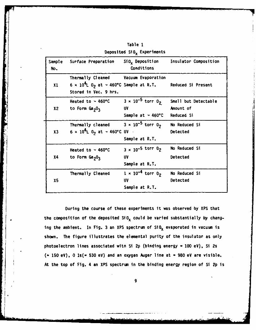
Table 1
Deposited SiO x Experiments
Sample Surface Preparation SiO x Deposition Insulator Composition
No. Conditions
Thermally Cleaned Vacuum EvaporationXl 6 x 10⁴L 02 at - 4600C Sample at R.T. Reduced Si Present
Stored in Vac. 9 hrs.
Heated to - 4600C 3 x 10⁻⁵ torr 02 Small but Detectable
X2 to Form Ga20 UV Amount of
Sample at - 460 0C Reduced Si
Thermally cleaned 3 x 1O- 5 torr 02 No Reduced Si
X3 6 x 10⁴L 02 at- 460C UV Detected
Sample at R.T.
Heated to - 4600C 3 x 10- 5 torr 02 No Reduced Si
X4 to Form Ga203 UV Detected
Sample at R.T.
Thermally Cleaned I x 10-4 torr 02 No Reduced Si
X5 UV Detected
Sample at R.T.
During the course of these experiments it was observed by XPS that
the composition of the deposited SiO x could be varied substantially by chang-
ing the ambient. In Fig. 3 an XPS spectrum of SiO x evaporated in vacuum is
shown. The figure illustrates the elemental purity of the Insulator as only
photoelectron lines associated wltn Si 2p (binding energy - 100 eV), Si 2s
(- 150 eV), 0 ls(- 530 eV) and an oxygen Auger line at - 980 eV are visible.
At the top of Fig. 4 an XPS spectrum in the binding energy region of Si 2p is
9
LI.

C3
CM
.6L
L
30
LL.
C4.
100

4-
IxSTARTING MATERIAL
3
2
2. -- . ..
VACUUM EVAP]S
xI O SURFACEIX1r-4TORRFLOE
a~ 1 Me ELECTRONS
... ",)-.
2
1 o**.. .*. .. 'I.
107 105 103 101 99 97 95
maera beor evpoato (mdde " afe" aum"vprto
and ,v
SX~x ": . • SRFAC__11

shown for the SiO x starting material (before evaporation). By using the chem-
ical shift scale of Adachi and Helms,5 the major Si 2p peak is identified as
S 4+ while the less intense peak is associated with SiP. Evaporation of this
same starting material in vacuum (or in - 10- 5 torr 02) produces a film which
contains reduced Si (spectrum in middle of Fig. 4). From the chemical shift
scale of Ref. 5, this reduced form of Si is most likely Si2+. Photochemical
reactions can be induced by ultraviolet (UV) excitation (see for e.g., the
discussion of A1203 growth on GaAs by evaporation of Al in 02 by Yokoyama et
al). 6 This possibility was investigated for the SiO deposition. Evaporation
of the SiO source material with the sample preparation chamber filled to
10-4-10- 5 torr of 02 which was illuminated by UV radiation produced in a film
with only one detectable Si oxidation state as indicated by the two XPS spec-
tra shown at the bottom of Fig. 4. This sample charged positively under
illumination by the XPS x-ray beam and consequently the relative binding-
energy scale cannot be compared directly with the spectra at the top and
middle of Fig. 4. The sample charging effect is easily observed by flooding
the sample surface with 5 eV electrons and noting the large shift in the ap-
parent Si 2p binding energy (see bottom of Fig. 4). The relative binding
energy difference between the Si 2p and 0 ls photoelectron peaks indicates
that this sample is S10 2 to within the analysis limits of the XPS technique.
The dielectric properties of the deposited SiO x improve markedly as
the amount of reduced Si is decreased. This observation will be noted further
in Section 111-1-b.
12

3. XPS Study of Aluminum Oxide Growth
Thermal oxidation of aluminum usually results in polycrystalline
oxide films of poor quality.7 We thus initiated a study to investigate the
growth of aluminum oxide by other methods with the desire to find a method
which would allow growth of Al oxide at room temperature. The preparation
methods were compared by using XPS. The initial studies include (A) slow
evaporation of Al in 02 background under UV Irradiation (Hg lamp), (B) and (D)
heating of film at - 510C under 02 exposure, (C) deposition of Al during 02
exposure on a heated substrate, and (E) deposition of Al under conditions of
02 plasma discharge onto a room temperature substrate. The XPS spectra in the
Al 2p region are shown in Figs. 5-7. The Al metal 2p level has a binding
energy of - 72.6 eV relative to the Fermi level. All spectra in Figs. 5-7 are
referenced to Al metal. Figure 5 shows the results for deposition under UV
Irradiation. This film is mostly Al metal but also has at least two different
oxides with chemical shifts of - 3.0 and - 2.0 eV, the former being similar to
the characteristic 2 2.8 eV shift of bulk A1203 and the latter being some
intermediate form of oxide. A slower deposition rate could possibly yield a
film that is totally oxide. Heating this film to - 5100C in 5 x 10⁻⁵ torr 02
almost totally converts this film to the intermediate oxide. Another film
investigated was one prepared by Al deposition in 1 x 10⁻⁴ torr 02 onto a
substrate at - 520C. This preparation leads to a mixture of Al metal and Al
oxide with the - 3.0 eV chemical shift and is thus similar to bulk oxide.
Again the deposition rate was probably too fast for total oxidation. Further
heating this film converts the film almost totally to aluminum oxide. The
13

.* cliC
IC 4
M22
*C CIO
* Cc
on C 4
4.1 0U
*CL -r-
LAL
an~
14-l

C4.3
044
2.L
CDC
U 060
.0L'0
A~r W~05J
Lin 41 &
4n- ou~
#AN C
4.DJ
x L. 0-LA c-4LI 4- 4 4
0
CCY
oC C1
LOE.
* n a. V^C4n. 2AITSNRNo

a--
41
.04
4J9-1
0410
O4j
0 ,-
C. 4LL
0
009, C CLcc wU C"
-F 4-
7- 6. 00
0 wO 4.)
:1~~~- % . aLAWa CL wl
00
*L Cox ieCAi. + 4.)

third preparation was Al deposition through a plasma discharge in 02 onto a
room temperature substrate. This sample was totally an aluminum oxide,
however, the chemical shift was - 1.4 eV. The intermediate oxide (with
chemical shift of - 1.4 eV) is typical of the initial stages of Al metal
oxidation at low 02 exposures9'10 and low temperatures.8 This is the first
observation in which a relatively thick film of the intermediate oxide was
prepared at room temperature. These investigations have shown that the
oxidation of Al is more complex than might first be expected. It is premature
to speculate on the chemical nature of the intermediate Al oxides.
In a previous report, 2 an investigation of the interaction of Al*
with native oxide on GaAs (100) was described. This initial work was extended
to include several other metals as part of an independent study. A manuscript
based on this work, which has been accepted for publication in Applied Physics
Letters, is reproduced in the Appendix. This work will also be discussed in
the Physics of Compound Semiconductor Interfaces Conference, January 27-29,
1981.
17

SECTION III
SAMPLE ANALYSIS
In the first part of this section, C-V and I-V measurements on samples
prepared as discussed in Sections I-1 and 11-2 are described. To facilitate
these measurements, metal dots of 10 and/or 20 ml diameters, were evaporated
onto the sample surfaces through a contact mask. The metal dots were - 200 A Cr
followed by - 2000 A of Au. The last part of this section describes depth
profiles for an oxidized portion of the MBE prepared sample No. 411.
1. C-V and I-V Measurements
a. MBE Samples
One promising approach to making a MIS structure on GaAs with a low
interface state density has been to grow a lattice matched AlxGal.xAs layer as
an insulator.1'11 Since such structures typically show large leakage
currents, an oxide is grown thermally to seal the structure against such
leakage.
As noted in Section 11-1 and the last interim report, 2 we have grown
a number of these samples in an attempt to reproduce the results of W.T. Tsang
et al1. C-V curves published by Tsang et al1 apparently show inversion and
accumulation with a low interface state density. However, as discussed in
Section IV of this report, these results may be controversial since they give a
18

smaller change in the surface potential for inversion than expected theo-
retically.
The results of C-V and I-V measurements on the MBE samples is
reported in this section. In the previous interim report 2 initial studies on
sample No. 411 were presented. In this report several new samples labeled No.
490, No. 491, and No. 493 have been investigated. Samples No. 490 and No. 493
are p-type whereas sample No. 491 is n-type.
The results for sample No. 491 are shown in Fig. 8. The C-V plot is
reminiscent 2 of data taken for sample No. 411. There is a large hysteresis
which depends on the direction of the scanning voltage. This hysteresis is
consistent with charge storage at the interface and has been discussed in the
previous report. 2 The effect of a longer oxidation anneal is shown in the
figure. There is only a small change between a 200 min and a 1040 min oxida-
tion which indicates a slightly thicker insulator for the longer oxidation.
These results indicate a complete oxidation of the AlAs and suggest that a
significant portion of the AllxGaxAs is also oxidized under these conditions.
The I-V measurements for sample No. 491 with a 200 min oxidation
indicate a leakage current of 10-9 amps at 6 volts forward bias for a 20 mil
dia. dot. The thickness of the insulating layer is not known but can be
estimated to be in excess of 2000 A.
The C-V characteristics for sample 490 are indicated in Fig. 9.
Although at first glance the sample appears to be going into inversion,
further analysis has shown that a more likely explanation is that the sample
19

00
% co
L)LA.Sb A
02

4)
EcoU
LAL
(jd) 0
21.'4
slum

has depleted through to the substrate. Such an interpretation was shown to be
correct by analyzing the C-V characteristics for a device with the thermal
oxide removed and a contact to the All.xGaxAs epilayer. The device was very
leaky but yielded a capacitance consistent with the width of the GaAs layer.
Sample No. 493 was similar to No. 490 but with a thicker, more
heavily doped GaAs layer. C-V measurements are shown in Fig. 10. There is a
small flat-band voltage shift of -0.6 volts for these samples which indicates
a positive interface charge. The samples show a small amount of hysteresis
but do not give any indication of inversion. The I-V curves indicate
breakdown at very low forward voltages of about -2 to -4 volts. Typically for
a forward voltage of -2 volts, currents of 3 x 10⁻⁸ amps are observed for a 20
mil diameter device. The thickness of the insulator is not known with great
certainty.
In the previous interim report,2 preparation and initial characteri-
zation of the MBE grown sample No. 411 was described (this sample is an at-
tempt to reproduce the structure reported in Ref. 1). A portion of this sam-
ple was oxidized sequentially for increasing lengths of time in an attempt to
move the oxide interface through the AlI.xGaxAs layer. After each sequential
oxidation a row of 10 mil dia dots was evaporated onto the sample and C-V
measurements were carried out at 1 MHz. The total accumulated oxidation times
were 10, 60, 330, 1575, and 10,455 min respectively. C-V measurements on the
initial sample (this sample has been superficially oxidized for - 0.5 min and
stored In a vacuum box since preparation) showed considerable nonuniformity In
behavior for different capacitors. A selected example Is shown in Fig. 11
22
I

CL
CA4-)-
4.3
C;-
o00N *1
CVLqkCuC
(id) 3
02

8
44_20 -10 V (Vol ts)
10-
RUN 1 -20 - 410 VOLTS.RUN 2 :-20 4 +10 VOLTS
5- RUN 3 STORED IN DARK 20 MNH. -20 *+10 VOLTS
-20 -10 0 10V (volts)
10-
RUN 1 : -20 -+10 VOLTS
L
5 RUN 4 MICROSCOPE LIGHT ON (30 SEC.). -20 -* +10 VOLTS
V (volts)
Fig. 11 c-v measurements at 1 -MHz for sample No. 411 after three sequentialoxidations, (top) 0.5 min oxidation, (middle) 10 min oxidation, and(bottom) 60 min oxidation.
* 24

(top). For the other five series of experiments, the uniformity of
characteristics was markedly better. In Fig. 11 (middle), a C-V measurement
is shown following the 10 min oxidation. The "oxide" capacitance has
increased substantially and there is a large hysteresis and shift of the flat-
band voltage due to interface charge storage (the interface charge decreases
noticeably after storage in the dark for many minutes). Figure 11 (bottom) is
a C-V measurement after 60 min of oxidation. Little change in characteristics
was observed as compared to the 10 min oxidation. It was observed that the
charge storage effect could be "erased" by exposure to microscope light.
Figure 12 (top) is a C-V measurement taken after 330 min of oxidation. Little
change in the C-V characteristics was observed as compared to the previous 2
sets of measurements. It was observed that the flat-band voltage was nearly a
linear function of forward-bias voltage applied to the sample. Figure 12
(bottom) is a C-V measurement obtained after 1575 min of oxidation. The C-V
characteristics are similar to the results for the previous 3 sets of
measurements, although an increase in oxide capacitance is observed which may
be significant. Figure 13 shows C-V measurements obtained after 10,455 min of
oxidation. The devices after this amount of oxidation were considerably more
leaky than the previous devices and forward breakdown occurred at - 8 volts.
A depth profile of this sample taken after the 10,455 min oxidation is
reported in Section 111-2.
In summary, sample No. 493 shows the most satisfactory C-V curves,
showing minimal hysteresis compared to the other structures. A persistent
problem with these devices is that the thermal oxide is very leaky,
25

SAW~LE 41110- 0NLDA
5 RIN 2-20 0 0OVOLTS
-20 -10 0 10V (VOLTS)
141
'a. 02, 400*C, 1575 MIN.RUN 1 -2D + 10 VOLTSRIM 2 :-20 4+10 VOLTS
6- RUN 3 :+10 -20 VOLTS
-20 -10V (VOLTS).
Fig. 12 C-V measurements at 1 MHz for same sample as in Fig. 11, (top) 330min oxidation, (bottom) 1575 min oxidation.
26

SAMPLE 411
12-1,55mv
10
-
RUN 1: -20 -+10 VOLTS
6- RUN 2: -20 - 10 VOLTS
RUN 3: +10 --20 VOLTS
20-10 10
V (VOLTS)
Fig. 13 C-V measurements at 1 M~z for same sample as in Figs. 11 and 12 after10,455 min oxidation.
27

effectively preventing inversion in any of the devices at present. One
approach which is being investigated is the use of various other insulators as
a substitute for the thermal oxide.
b. Deposited Insulator Samples
As discussed in Section 11-2 several samples were prepared and
studied after SiO x deposition in the XPS apparatus. Results of C-V and I-V
measurements on these samples are presented here. Both p-type and n-type
samples were prepared.
In the first of these samples, X1, a few monolayers of Ga2 03 were
formed by heating the GaAs surface to - 4600C during exposure to 6 x 10⁴ L of
oxygen. This was followed by vacuum evaporation of - 1000 A of SiO x. Metal
dots were subsequently evaporated onto the samples and 1 MHz C-V measurements
and I-V measurements were performed.
Typical results are shown in Fig. 14 for C-V measurements on these
samples. For the p-type sample a deep depletion curve is observed for a large
positive bias. Although the estimated change in the surface potential is
large enough for inversion to occur, leakage through the oxide apparently
prevents accumulation of electrons in the inversion layer. 12 At reverse bias
the device appears to go into accumulation. The n-type sample shows a C-V
curve which is not interpretable by standard methods. Although the curve
shows some indication of deep depletion, no accumulation or inversion behavior
is identifiable.
28

20MI DI.
40 -7o~~
30?
40
30
-30-20 -10 0.1V (VOLTS)
Fig. 14 c-v measurements at 1 M4Hz for sample XI.
29
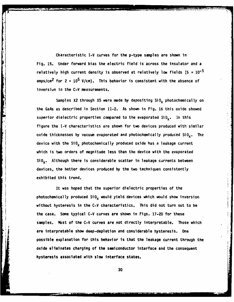
Characteristic I-V curves for the p-type samples are shown In
Fig. 15. Under forward bias the electric field is across the insulator and a
relatively high current density is observed at relatively low fields (5 x 10⁻⁵
amps/cm2 for 2 x 10⁵ V/cm). This behavior is consistent with the absence of
inversiun in the C-V measurements.
Samples X2 through X5 were made by depositing Si0 x photochemically on
the GaAs as described in Section 11-2. As shown in Fig. 16 this oxide showed
superior dielectric properties compared to the evaporated SiO x. In this
figure the I-V characteristics are shown for two devices produced with similar
oxide thicknesses by vacuum evaporated and photochemically produced SiO x. The
device with the SiO x photochemically produced oxide has a leakage currentwhich is two orders of magnitude less than the device with the evaporated
SiO x. Although there is considerable scatter in leakage currents between
devices, the better devices produced by the two techniques consistently
exhibited this trend.
It was hoped that the superior dielectric properties of the
photochemically produced SiO would yield devices which would show inversion
without hysteresis in the C-V characteristics. This did not turn out to be
the case. Some typical C-V curves are shown in Figs. 17-20 for these
samples. Most of the C-V curves are not directly interpretable. Those which
f are interpretable show deep-depletion and considerable hysteresis. One
possible explanation for this behavior is that the leakage current through the
oxide eliminates charging of the semiconductor Interface and the consequent
hysteresis associated with slow interface states.
30

10-
FORWARD
L20NL DIA.
'~10-8
10-9
iO1O~V (VOLTS)
02 6 10
Fig. 15 I-V measurements for sample X1 (p-type).
31

10-6
VACUUMEVAPORATED
10-7
-0.020 IN. DJA.
10-8 -METAL DOTON GAs (100)P-TYPE (2x10¹⁶cpf3)
-1019
10-11-
PHOTOCHEMI CALLYPRODUCED
10-12
10-13.1- 6-
0 2-4- 8-10V (VOLTS)
Fig. 16 Comparison of leakage currents for vacuum~ evaporated Si0,x and
photochemnically produced SiO 2 insulators.
32
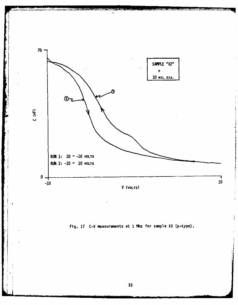
70
SAPL "28P~i~
RUN 1: 10 -- 10 VOLTS
RUN 2: -10 -10 VOLTSI
0-10 10
V (VOLTS)
Fig. 17 c-v measurements at 1 14Hz for sample X2 (p-type).
33

SAMPLE 'X3*
RUN 1: -20 - +20 VOLTS (RAmp-1.5 v/s) [20 MIL DIA.
RUN 2. +20 --20 VOLTS (RAmw -1.5 v/s)
RUN 3: -20 -+20 VOLTS (RAqp- '0.3 v/s)
RUN 4:. +20 --20 VOLTs (RAM4P -0.3 vls)
+20-20
Fig. 18 C-V measurements at 1 MHz for sample X3 (p-type).
34

75
-% SAMPLE IV4
20 MIL-DIA.
0--10 V (VOLTS) 10
Fig. 19 C-V measurements at 1 M4Hz for sample X4 (n-type).
35

100
IN
0.I
15vo~s +15
Fig. 20 c-v measurements at 1 MHz for sample X5 (n-type).
36

One of the samples, X3, which showed good leakage characteristics was
sent for evaluation to Dr. B. Bayraktaroglu at the Air Force Wright
Aeronautical Laboratories (AFSC) where frequency dependent C-V and G-V
measurements were made.13 Hysteresis in the C-V and G-V curves was observed.
The C-V curves were difficult to study due to the small change in capacitance
with applied voltage. The G-V curves produced distinct peaks at all test
frequencies. Such peaks indicate the presence of states at the interface.
,* Typical examples of some of these data are shown in Figs. 21 and 22.
In conclusion, none of the SiO x insulating layers currently inves-
tigated was capable of satisfactorily passivating the GaAs surface suitably
for device applications. Inversion was not observed for any device while only
devices with unacceptably large leakage showed interpretable C-V curves
without hysteresis.
2. Depth Profile of Sample No. 411
At the conclusion of the series of sequential oxidations carried out
on Sample No. 411 (see Sections II-1 and III-1-a) a scanning Auger microprobe
(SAM) depth profile was obtained by a series of sputter-Auger analysis
steps. The SAM instrumentation has been previously described.2 The result of
this Ar+ sputtering depth profile is presented in Fig. 23.
The sputter time axis of Fig. 23 is related to depth within the
sample and the sputter rate is - 20 A/min. The graded Al1 xGaxAs layer is
37

503
11M*
3 oSEC WTe BETWEEN
I READINS
U
Fig. 21 c-v measurements at I Mtiz for sample X3 (n-type). Data obtained byB. Bayraktaroglu (WPAFB).
38

X3N
100 k~z1V STEPS1 SEC. WAIT BETWEEN
READI NGS
0[I a U
Fig. 22 G-V measurements at 100 kHz for sample X3 (n-type). Data obtainedby B. Bayraktaroglu (WPAFB).
39

%.(%
4.)
*Q %
1 404-)-
r- 00 3
%*- CDE
to L0)
C~CJO0N Q
a= CDl
CDC
400
reached after sputtering - 4 x 10³ s while the GaAs layer is reached after
9 X 10³ s of sputtering. The important result is that the oxygen signal
extends all the way to the GaAs layer and seems to decrease at approximately
the same rate as the Al signal. Therefore, after 10,455 min of oxidation,
this sample appeared to be oxidized completely through the graded Al1 xGaxAs
layer.
Ah XPS depth profile was also obtained on this same sample.
Difficulties experienced in aligning the sputter crater and the x-ray beam
made this profile a bit more difficult to interpret although the basic
conclusions are the same as those drawn from the SAM profile (Fig. 23). The
XPS data obtained within the graded All.xGaxAs layer showed that the Al was
oxidized while the Ga was not oxidized. Although this result could be an
artifact of the sputtering process our previous experience suggests that this
explanation is unlikely.
41
SECTION IV
DISCUSSIONS OF PREVIOUS MBE RESULTS
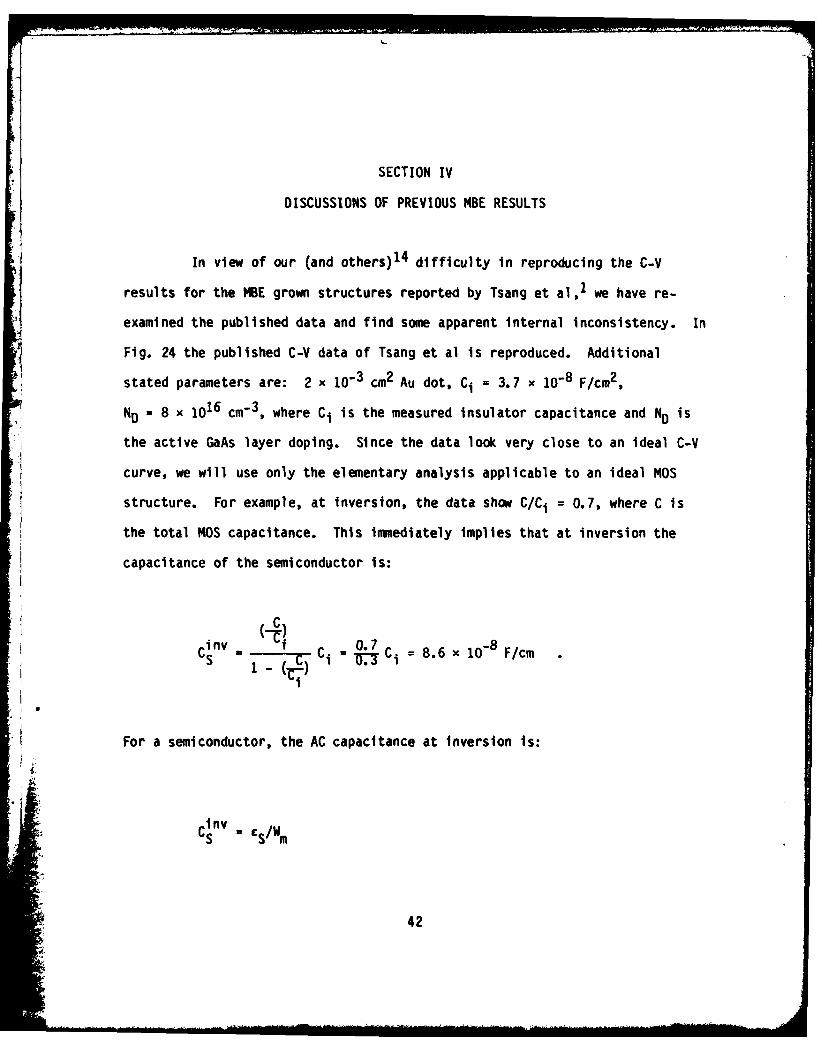
In view of our (and others)14 difficulty in reproducing the C-V
results for the MBE grown structures reported by Tsang et al, 1 we have re-
examined the published data and find some apparent internal inconsistency. In
Fig. 24 the published C-V data of Tsang et al is reproduced. Additional
stated parameters are: 2 x 10⁻³ cm2 Au dot, Ci = 3.7 x 10⁻⁸ F/cm2,
ND = 8 x 1016 cm-3 , where Ci is the measured insulator capacitance and ND is
the active GaAs layer doping. Since the data look very close to an ideal C-V
curve, we will use only the elementary analysis applicable to an ideal MOS
structure. For example, at inversion, the data show C/Ci = 0.7, where C is
the total MOS capacitance. This immediately implies that at inversion the
capacitance of the semiconductor is:
C
fly 1 C0.7 8C ) C-i Ci =8.6 x 10- F/cm
For a semiconductor, the AC capacitance at inversion is:
C invCs cs/Wm
42

where Wm is the depletion width and eS . 1.11 x 10⁻¹² F/cm2 , the dielectric
constant for GaAs. Thus, Wm - 1.11 x 10⁻²/8.6 x 10-8 = 1.29 x 10⁻⁵ cm
1290 A is the measured value for Wn"
This value for Wm must be consistent with:
Wm= (2sV tnv/qND )l12
which is the depletion width at inversion as a function of doping. For GaAs,
Yin v - 1.4 V, thus,S
= nv 2i 17 3
ND 2csV S /qWm 2 1.13 x 10 cm 3
is the actual measured value for ND. This is consistent with the stated value
of 8 x 1016 cm-3.
The other parameter directly available from Fig. 24 is the gate
voltage, Vg, at inversion, which is measured as 2.1 V. This value of Vg
should be compatable with:
invlVg - (Q8/Ci) + nv
43

QS -2x10 10 4:3i-2
VFB O-O.1V
1.07
C'CTOTA. AlAs -oxidized 1000OA
Al xialXAs 1200A____________ X 0.5-1.0
1 M~z
0.5-- GaAs
N D =801016 cm-3
[Wi. T. Tsang. M. Olmstead, IR. P. H. Chang; Appi. Phys. Lett 3,408. 1979]
-6 -4 -2 0 2 4 6 8
VOLTS
Fig. 24 c-v measurements for thermally oxidized MBE grown sample ofAlAs/graded A1xGal...As/GaAs replotted from Ref. 1.
44

which states that the voltage across the insulator and semiconductor equals
the gate voltage at inversion, QB = (2"qNDV~nv)l/2 = 2.3 x - Co ul/cm2.
Thus (QB/Ci) = 6.3 V (5.4 V for the quoted 8 x 1016 cm-3 doping). In the
absence of significant interface charge, which the data show to be the case,
this simple analysis indicates that although the capacitance values measured
for "flatband" and "inversion" are consistent with the stated oxide thickness
and n-type layer doping, the gate bias at inversion should be - 7 V rather
than the - 2V shown. Interface charge would increase Vg thus our calculated
Vg is a minimum value. We presently have no explanation for the low gate
voltage at inversion shown in the data.
- 4
-1 ~'
• 45

REFERENCES
1. W.T. Tsang, M. Olmstead, and R.P.H. Chang, Appl. Phys. Lett. 34, 408
(1979).
2. R.W. Grant, J.R. Oliver, S.P. Kowalczyk, J.R. Waldrop and D.L. Miller,
Technical Report AFWAL-TR-80-1104.
3. R. Dingle, W. Wiegmann, and C.H. Henry, Phys. Rev. Lett. 33, 827 (1974).
4. R.W. Grant, S.P. Kowalczyk, J.R. Waldrop, and W.A. Hill, in The Physics
of MOS Insulators, p. 202 (Pergamon Press, New York, 1980) edited by G.
Lucovsky, S.T. Pantelides, and F.L. Galeener.
5. T. Adachi and C.R. Helms, J. Electrochem Soc. 127, 1617 (1980).
6. S. Yokoyama, K. Yukitomo, M. Hirose, and Y. Osaka, Thin Solid Films 56,
81 (1979).
7. P. Kofstad, High-Temperature Oxidation of Metals (Wiley, New York, 1966).
8. A.F. Carley and M.W. Roberts, Proc. R. Soc. Lond A363, 403 (1978).
4
i 46
°*,

9. S.A. Flodstrom, R.Z. Bachrach, R.S. Bauer, and S.B.M. Hagstrom, Phys.
Rev. Letters 37, 1282 (1976).
10. A. Bianconi, R.Z. Bachrach, S.8.M. Hagstrom and S.A. Flodstrom, Phys.
Rev. 19, 2837 (1979).
11. H.C. Casey, Jr., A.Y. Cho, and E.H. Iicollian, Appl. Phys. Lett. 32, 678
(1978).
12. For a discussion of C-V measurements and their interpretation, see A.S.
Grove, B.E. Deal, E.H. Snow, and C.T. Sah, Solid St. Electronics 8, 145
* (1965).
13. G-V measurements are discussed in the literature by E.H. Nicollian and A.
Goetzberger, Bell Syst. Tech. Jour. 46, 1055 (1967).
14. H.C. Casey, Jr., A.Y. Cho, and H. t'brkoc; G.Y. Robinson, L.P. Erickson,
* T.E. Brady, and T.R. Ohnstein, work reported at the "Workshop on
Dielectric Systems for the III-V Compounds -1980" San Diego, Calif.
May 20-21, 1980.
* 47

APPENDIX
The manuscript reproduced here will be published in the February 1,
1981 is.,e of Applied Physics Letters.
48'
48
REACTIVITY AND INTERFACE CHEMISTRY DURING SCHOTTKY-BARRIER FORMATION:
METALS ON THIN NATIVE OXIDES OF GaAs INVESTIGATED BY XPS
Steven P. Kowalczyk, J. R. Waldrop and R. W. Grant
Rockwell International Electronics Research Center
Thousand Oaks, CA 91360
ABSTRACT
The room temperature interfacial chemical reactions of overlayers of
several diverse metals (Au, Cu, Al, Mg, Cr, and Ti) with thin native oxide
films (- 10 A) on GaAs (100) surfaces were investigated with x-ray
photoelectron spectroscopy (XPS). The reactivity of these metals with the
native oxides of GaAs ranged from inert to complete reduction of the oxides
and is well predicted by bulk thermodynamic free energies of formation.
Variations in band bending during Schottky-barrier formation were monitored by
XPS. The implication of the observed interface chemistry for Schottky-barrier
modeling is discussed.
Schottky-barrier junctions are the basis of a large number of com-
pound semiconductor electronic devices, including microwave diodes, FET's,
solar cells, photodetectors, and CCD's; thus, knowledge of interfacial
49I

phenomena occurring during formation of Schottky-barrier contacts is of
significant importance. A fundamental understanding of these phenomena is
especially crucial as the prospect of very large scale integrated circuit
technology becomes imminent. The primary experimental thrust of surface
science experiments has been limited to ideal (abrupt) contacts, that is,
metals deposited under ultra-high vacuum (UHV) conditions on atomically clean
and crystallographically ordered semiconductor surfaces.1-5 However, typical
fabrication procedures for a Schottky-barrier device generally are such that a
native oxide film is present on the semiconductor surface prior to metal
deposition. For this reason modeling of practical Schottky-barrier devices
generally assumes the presence of a thin (10-100 A) interfacial insulator film
between the metal and semiconductor.6
This letter reports x-ray photoelectron spectroscopy (XPS) investiga-
tions of Schottky-barrier formation at GaAs (100) interfaces in the presence
of a thin native oxide surface layer. GaAs surfaces that had two different
initial oxides were studied. The room temperature chemistry was investigated
for the metals Au, Cu, Al, Mg, Cr, and Ti with an interfacial oxide layer
during sequential stages of contact formation. A range of reactivity was
found, from chemically inert (Cu and Au) to complete consumption of the native
oxide layer (Al, Mg, Cr, and Ti). We have also used XPS to monitor the GaAs
interface band bending during Schottky-barrier formation and find that the
Schottky-barrier height is relatively independent of the composition of the
initial thin native oxide layer.
s0

The ability of XPS to detect the chemical state of the component
atomic species in a molecule or solid is well known,7 including numerous ap-
plications to surface chemistry.8 ,9 The surface sensitivity of XPS is due to
its - 25 A sampling depth. The capability of XPS to monitor surface - or
interface - potentials to high accuracy is less well known.10,11 Chemical
information is obtained from chemical shifts of core-level binding energies.
These shifts are the result of changes of valence-electron distribution. For
example, the binding energy of the As 3d level in As203 is - 3.4 eV higher
than in GaAs. For a semiconductor, band bending rigidly shifts all core-level
binding energies with respect to the Fermi level, thus one can monitor the
potential shift of a particular valence state to measure interface
potentials. Details of potential-shift measurement and its application to
interface potentials can be found in Ref. 11. The present work utilizes both
capabilities.
The XPS instrumentation used for these measurements is a HP 5950A
electron spectrometer with monochromatized AlKa (hv = 1486.6 eV) x-ray source
and UHV modifications ((9 x 10-11 torr). The sample treatment chamber in-
cluded an evaporator and a quartz crystal thickness monitor for controlled
metal depositions. The sample holder incorporates a resistive heater capable
of producing sample temperatures up to 1000C.
The samples were all bulk grown n-type (- 5 x 1016 cm- 3 ) GaAs 1 2 which
had been wafered and polished to give a (100) surface. Two types of GaAs
(100) surfaces were prepared. Each surface was first treated with a standard
sulfuric 4:1:1 (H2SO4, H202, H20) etch for approximately 1 minute, quenched in
51

H20, then inserted into the introduction chamber of the XPS spectrometer
system within a few minutes. XPS analysis of relative peak heights shows that
this procedure results in a - 10 A thick mixed oxide consisting of both As203
and Ga203 (see Fig. 1) and an associated large surface band bending (- 0.7
eV). 1 1 A second set of samples with a different type of oxide was prepared by
heating the above mixed oxide to - 4500C in a vacuum of 10-9 torr for - 5
minutes. Such sample heating could occur during a device processing step.
This heat treatment results in a surface oxide layer with about the same
thickness but solely with the composition Ga203 from the reaction:
As203 + 2 GaAs + Ga203 + 2 As2 t (1)
in which additional GaAs substrate is consumed.11 The Ga203 covered surface
is associated with a low band bending (- 0.3 eV).11 ,13 The difference in
surface potential is - 0.4 eV between these two surfaces. A sample with each
of the oxides was prepared for deposition of the metals Au, Cu, Al, Mg, Ti,
and Cr. Three regimes of deposited metal thickness were studied: (1)
submonolayer, (2) - 1-3 monolayer and (3) thick, > 50 A.
In Fig. 1 the XPS Ga 3d, As 3d, and Al 2p core-level peaks are shown
for the initial mixed oxide surface, (a), and for four successive Al metal
depositions, (b)-(e), which were made onto a mixed-oxide covered GaAs
substrate. The peaks arising from the Ga and As in the GaAs substrate
(labeled Ga(GaAs) and As (GaAs)) are clearly distinguishable from the
chemically shifted Ga and As contributions arising from the thin oxide film
52

(labeled Ga(ox) and As(ox)). With the first two depositions of Al, - 5 A,
(b)-(c), the Al consumes As203 and becomes A1203 via the room temperature
solid-state reaction:
2 A1 + As203 + A1203 + As2 +, (2)
the Ga203 is unaffected. The elemental As produced is apparently desorbed
from the surface. Once the As203 is entirely consumed, additional Al,
deposited in (d)-(e), reacts with the Ga203 via the reaction:
2 Al + Ga203 + A1203 + 2 Ga . (3)
In spectrum (e) the elemental Ga produced by this reaction is apparent as a
low binding-energy peak at - 18.3 eV; also, only when both oxides are
completely reduced is metallic Al observed, as in (d) and (e). The total
amount of Al deposited was - 40 A.A similar sequence of depositions were made
for Ti, Cr, Au, and Cu metal overlayers. Ti and Cr were more reactive than A
in that both oxides were reduced simultaneously rather than sequentially, the
chemical behavior was otherwise similar. For Au and Cu deposition, on the
other hand, neither oxide was chemically affected, no reduction of oxide was
observed. All surfaces which had the mixed As203 and Ga203 oxides exhibited
little change of surface band bending upon deposition of metal overlayers.
In Fig. 2 a series of Ga 3d peaks (a)-(e) from GaAs substrates that
had the Ga203 surface are shown for a - 15 A deposition, labeled (2), of Al,
534

Ti, Cr, Au, and Cu, respectively. In all the initial spectra, labeled (1),
the pronounced shoulder on the high binding-energy side of the Ga(GaAs) main
peaks is due to the Ga203 oxide film. In this series of spectra both chemical
effects and a GaAs band-bending change are evident as a result of metal
deposition. For example, in cases (a)-(d) a binding-energy shift of the main
Ga(GaAs) peaks to - 0.4 eV lower binding energy is readily discernable. As
discussed earlier, this type of shift corresponds to a change in band-bending
potential in the GaAs. In this case, we are observing a change in interface
band bending in the GaAs as a Schottky-barrier contact is being formed by the
presence of a metal. For Al, Ti, and Cr, (a)-(c) this band-bending change is
accompanied by Ga203 reduction and the formation of Ga alloys or compounds
with the deposited metal, as evidenced by disappearance at the Ga(ox) shoulder
and the appearance of the low binding-energy structure. Although not shown,
Mg metal overlayers had identical behavior. Once again, Au and Cu produced no
chemical reaction with the Ga203 layer, although a significant increase in
GaAs band bending still occurs.
The driving force for these chemical reactions is the change in free
energy of formation AG. The use of bulk AG values provides a useful rule-of-
thumb 9 for predicting all of the interfacial reactions observed in this
work. However, because this predictive guide is based on bulk thermodynamic
properties and does not consider interfacial contributions it should be
employed with caution.
Our results have several implications for understanding the formation
of Schottky-barrier contacts. Two of the important aspects of this work are
54

that, (1) the chemical reactivity and (2) the pinning position of the surface
Fermi level can both be contactlessly monitored in the same XPS measurement
during contact formation. Figure 1 shows that an initial layer of native
oxide is completely consumed by reaction with certain deposited metals at room
temperature to thus produce a new and different oxide (such as A1203 in Fig.
1). Figure 2 demonstrates another important concept, namely that a band-
bending variation can occur during Schottky-barrier contact formation in the
presence of a surface oxide. If a surface is prepared with a low surface band
bending (such as the Ga203 surface of Fig. 2), the deposition of metal on the
thin native oxide layer acts to shift the surface Fermi level to result in a
higher band bending and thus a higher Schottky-barrier height. This new
pinning position is approximately the same whether there is a chemical
reaction (Ti, Cr, Al, Mg) or not (Au and Cu). Thus the distinct interfacial
native oxide which is conventionally assumed in present Schottky models either
does not exist or does not insulate the semiconductor from the effects of a
metal overlayer. Therefore the interfacial oxide layer as is presently used
in modeling Schottky-barrier heights is not appropriate for GaAs.
Since GaAs is a prototypical covalent compound semiconductor, we
expect that the observed interface effects are general phenomena on compound
semiconductor surfaces. We note that the metals which react with native
oxides may be preferred in actual devices because they would have presumably
better contact adhesive properties.
55

ACK NOWL EDGMENT
This work was supported in part by WPAFB Contract No. F33615-78-C-
1591. We thank Dr. Peter Asbeck for informative discussion.
56

REFERENCES
1. R. H. Williams, V. Montgomery, and R. R. Varma, J. Phys. C 11, 1735(1978).__
2. J. R. Waldrop and R. W. Grant, Appi. Phys. Lett. 34, 630 (1979).
3. P. W. Chye, I. Lindau, P. Planetta, C. M. Garner, C. Y. Su, and W. E.Spicer, Phys. Rev. B 18, 5545 (1978).
4. K. Okuno, T. Ito, M. Iwami, and A. Hiraki, Sol. St. Conm. 34, 493 (1980).
5. L. J. Brillson, Phys. Rev. B 18, 2431 (1978).
6. See, for example, S. M. Sze, Physics of Semiconductor Devices, (Wiley-Intersclence, New York 1969).
7. K. Siegbahn, C. Nordling, A. Fahlman, R. Nordberg, K. Hamrin, J. Hedman,G. Johansson, T. Bergmark, S.-E. Karlsson, I. Lindgren, and B. Llndberg,ESCA Atomic, Molecular, and Solid State Structure Studied by Means ofElectron Spectroscopy, (Nova Acta Regiae Soc. Scl. Upsallensis ser. IV,20, 1967).
8. C. R. Brundle, Sur. Sci. 48, 99 (1975).
9. N. Winograd, W. E. Baltinger, J. W. Amy, and J. A. Munarin, Science 184,565 (1974).
10. E. A. Kraut, R. W. Grant, J. R. Waldrop and S. P. Kowalczyk, Phys. Rev.Lett. 44 1620 (1980).
11. R. W. Grant, S. P. Kowalczyk, J. R. Waldrop and W. A. Hill, in Physics ofMOS Insulators ed. S. Pantelides, (American Institute of Physics, New
olrk, to be published).
12. From Crystal Specialities, Inc.
13. A Ga 0 surface layer can alternatively be prepared by heating the initialoxdi io - 570C in UHV for several minutes to produce a clean surface(which gives a caracteristtc LEED pattern) and subsequent oxidation byexposure to 10" L 02 at 4800C.
57

IV
*11Is .1
I1*cz
SrCZ
No C:-4. ac.O
C0-q
4z 4,- .!e
/1 *I.amoft1O
ii4 ICIII.Y
U.
01~) S.linfl0

20 a) . Al
10 .(2)
(1)V x2.5
02 (b) (1) f, Ti
o (-'2).
/ i _-...2.510 - \ XAu20
~~(1)' , l
0 'r
" 10 (
*1 ' \'N x2.5.
0!
(d) Au10 */ \(2)
10 Cu
* 0AM
22 20 .18
BINDING ENERGY (eV)
Fig. 2 The Ga 3d spectra of heat treated n-GaAs (100) with Ga ,0 surfacelayer. (1) Before metal deposition and (2) after metat 4eposition.Metals: (a) Al, (b) Ti, (c) Cr, (d) Au and (e) Cu.
.59