processors, fpgas, and asics - columbia universitysedwards/classes/2008/4840/processors.pdf ·...
TRANSCRIPT

Processors, FPGAs, and ASICs
Prof. Stephen A. Edwards
Columbia University
Spring 2008
Processors, FPGAs, and ASICs – p.
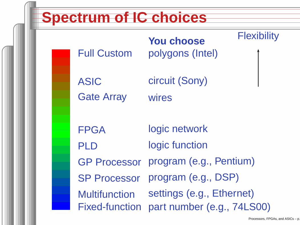
Spectrum of IC choices
Full Custom
ASIC
Gate Array
FPGA
PLD
GP Processor
SP Processor
MultifunctionFixed-function
You choosepolygons (Intel)
circuit (Sony)
wires
logic network
logic function
program (e.g., Pentium)
program (e.g., DSP)
settings (e.g., Ethernet)part number (e.g., 74LS00)
Flexibility
Processors, FPGAs, and ASICs – p.

NMOS Transistor Cross Section
pn+
n+
Al
oxpoly Al
Processors, FPGAs, and ASICs – p.

Inverter Transistors and Layout
x
x
Vdd
Vssx
Vss
Vdd
x
Processors, FPGAs, and ASICs – p.
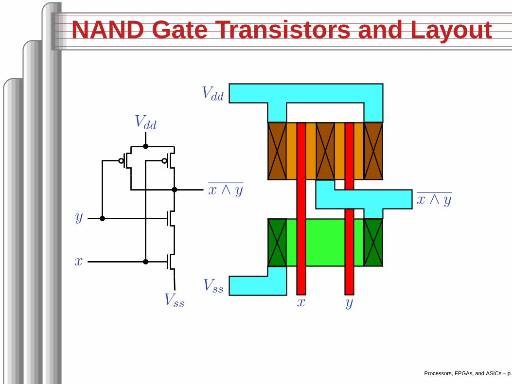
NAND Gate Transistors and Layout
x ∧ y
x
y
Vdd
Vss x yVss
Vdd
x ∧ y
Processors, FPGAs, and ASICs – p.

Full-custom ICs
Processors, FPGAs, and ASICs – p.

Standard Cell ASICs
Processors, FPGAs, and ASICs – p.

Standard Cell ASICs
Processors, FPGAs, and ASICs – p.

Channeled Gate Arrays
Processors, FPGAs, and ASICs – p.

Channeled Gate Arrays
Processors, FPGAs, and ASICs – p. 10

Sea-of-Gates Gate Arrays
Processors, FPGAs, and ASICs – p. 11

FPGAs: Floorplan
DLL DLL
DLLDLL
BLO
CK
RA
MB
LOC
K R
AM
BLO
CK
RA
MB
LOC
K R
AM
I/O LOGIC
CLBs CLBs
CLBs CLBs
DS077_01_052102
Processors, FPGAs, and ASICs – p. 12
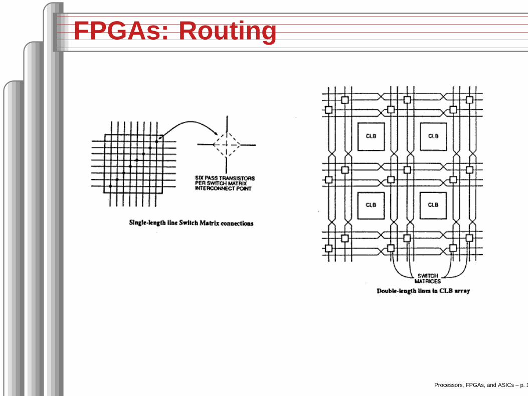
FPGAs: Routing
Processors, FPGAs, and ASICs – p. 13

FPGAs: CLB
I3
I4
I2
I1
Look-UpTable
D
CK
EC
Q
R
S
I3
I4
I2
I1
O
O
Look-UpTable
D
CK
EC
Q
R
SXQ
X
XB
CE
CLK
CIN
BX
F1
F2
F3
SR
BY
F5IN
G1
G2
YQ
Y
YB
COUT
G3
G4
F4
Carryand
ControlLogic
Carryand
ControlLogic
Processors, FPGAs, and ASICs – p. 14

PLAs/CPLDs: The 22v10
0 4 8 12 16 20 24 28
Increments
FirstFuseNumbers
32 36 40
Macro-cell
R = 5809P = 5808
R = 5811P = 5810
R = 5813P = 5812
R = 5815P = 5814
Asynchronous Reset
23
22
21
20
1
2
3
4
(to all registers)
396
0
440
880
924
1452
1496
2112
I/O/Q
I/O/Q
I/O/Q
I/O/Q
I
I
I
CLK/I
Macro-cell
Macro-cell
Macro-cell
Processors, FPGAs, and ASICs – p. 15

Example: Euclid’s Algorithm
int gcd(int m, int n){int r;while ((r = m % n) != 0) {
m = n;n = r;
}return n;
}
Processors, FPGAs, and ASICs – p. 16
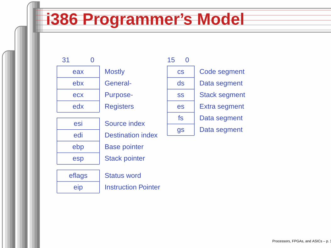
i386 Programmer’s Model
31 0
eax Mostly
ebx General-
ecx Purpose-
edx Registers
esi Source index
edi Destination index
ebp Base pointer
esp Stack pointer
eflags Status word
eip Instruction Pointer
15 0
cs Code segment
ds Data segment
ss Stack segment
es Extra segment
fs Data segment
gs Data segment
Processors, FPGAs, and ASICs – p. 17

Euclid on the i386
gcd: pushl %ebpmovl %esp,%ebppushl %ebxmovl 8(%ebp),%eaxmovl 12(%ebp),%ecxjmp .L6
.L4: movl %ecx,%eaxmovl %ebx,%ecx
.L6: cltdidivl %ecxmovl %edx,%ebxtestl %edx,%edxjne .L4movl %ecx,%eaxmovl -4(%ebp),%ebxleaveret
Processors, FPGAs, and ASICs – p. 18
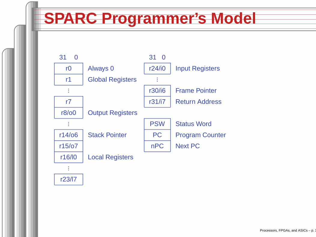
SPARC Programmer’s Model
31 0
r0 Always 0
r1 Global Registers...
r7
r8/o0 Output Registers...
r14/o6 Stack Pointer
r15/o7
r16/l0 Local Registers...
r23/l7
31 0
r24/i0 Input Registers...
r30/i6 Frame Pointer
r31/i7 Return Address
PSW Status Word
PC Program Counter
nPC Next PC
Processors, FPGAs, and ASICs – p. 19

SPARC Register Windows
The outputregisters of thecalling procedurebecome the inputsto the calledprocedure
The global registersremain unchanged
The local registersare not visibleacross procedures
r8/o0...r15/o7r16/l0...r23/l7
r8/o0 r24/i0... ...r15/o7 r31/i7r16/l0...r23/l7
r8/o0 r24/i0... ...r15/o7 r31/i7r16/l0...r23/l7r24/i0...r31/i7
Processors, FPGAs, and ASICs – p. 20

Euclid on the SPARC
gcd:save %sp, -112, %spmov %i0, %o1b .LL3mov %i1, %i0mov %i0, %o1b .LL3mov %i1, %i0
.LL5:mov %o0, %i0
.LL3:mov %o1, %o0call .rem, 0mov %i0, %o1cmp %o0, 0bne .LL5mov %i0, %o1retrestore
Processors, FPGAs, and ASICs – p. 21
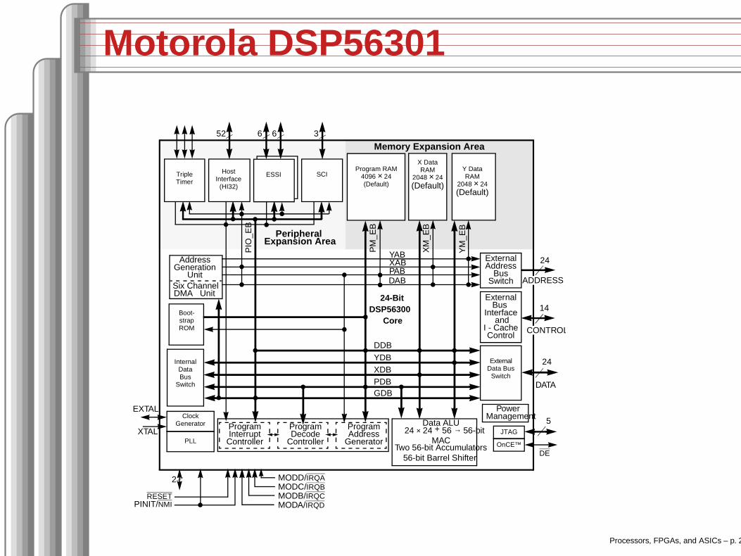
Motorola DSP56301
Figure 1-1. DSP56301 Block Diagram
PLL OnCE™
ClockGenerator
Internal DataBus
Switch
Program RAM4096 × 24(Default)
YABXABPAB
YDBXDBPDBGDB
MODC/IRQBMODB/IRQC
ExternalData Bus
Switch
14
MODA/IRQD
DSP56300
652
24-Bit
24
24
X DataRAM
2048 × 24(Default)
Y DataRAM
2048 × 24(Default)
DDB
DAB
Memory Expansion Area
Peripheral
Core
YM
_EB
XM
_EB
PM
_EB
PIO
_EB
Expansion Area
6
SCI
JTAG
3
RESET
MODD/IRQA
PINIT/NMI
2
Boot-strapROM
EXTAL
XTAL
ADDRESS
CONTROL
DATA
TripleTimer
HostInterface
(HI32)
ESSI
AddressGeneration
UnitSix ChannelDMA Unit
ProgramInterrupt
Controller
ProgramDecode
Controller
ProgramAddress
Generator
Data ALU24 × 24 + 56 → 56-bit
Two 56-bit Accumulators56-bit Barrel Shifter
PowerManagement
ExternalBus
Interface and
I - CacheControl
ExternalAddress
BusSwitch
5
DE
MAC
Processors, FPGAs, and ASICs – p. 22

DSP 56000 Programmer’s Model
55 4847 2423 0x1 x0 Sourcey1 y0 Registers
a2 a1 a0 Accumulatorb2 b1 b0 Accumulator
15 0r7...r4r3...r0
15 0n7...n4n3...n0
15 0m7...m4m3...m0
AddressRegisters
15 0Program CounterStatus RegisterLoop AddressLoop Count
15 PC Stack...0
15 SR Stack...0
Stack pointer
Processors, FPGAs, and ASICs – p. 23
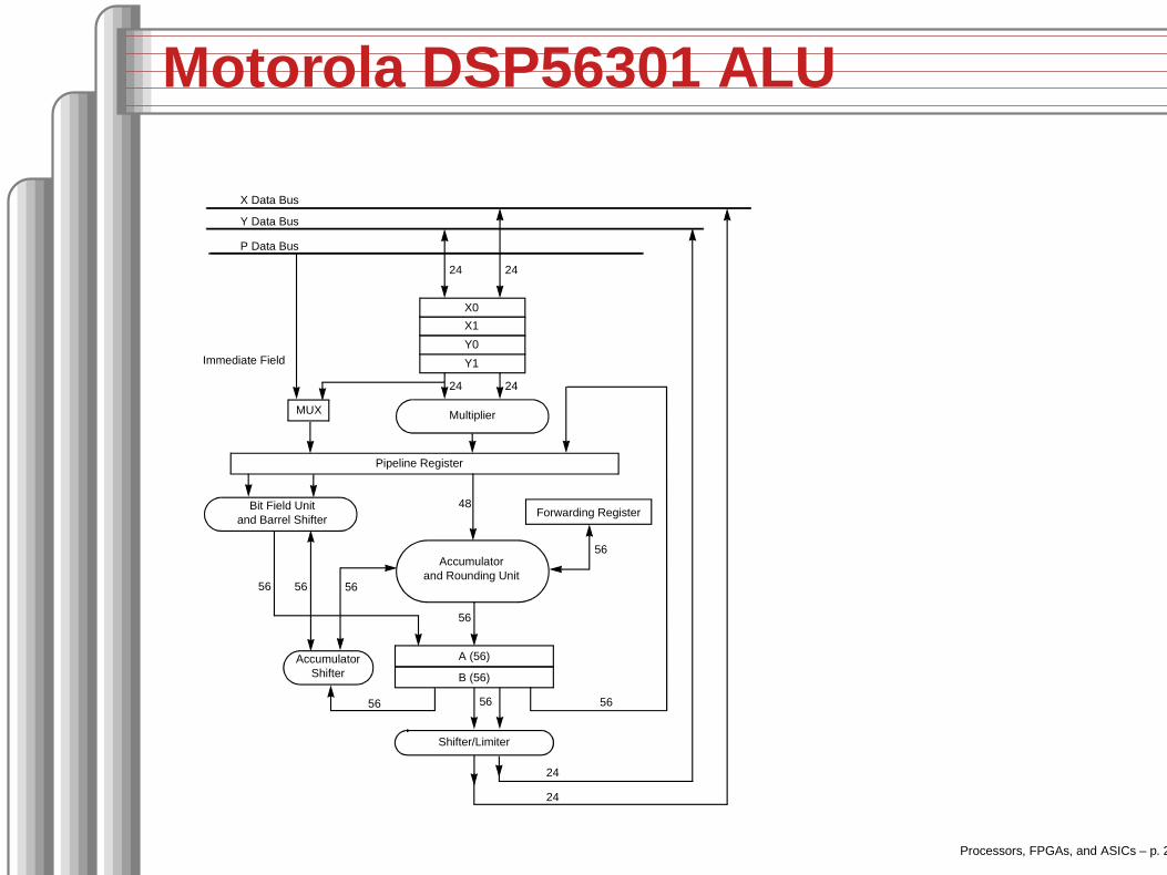
Motorola DSP56301 ALU
Bit Field Unit and Barrel Shifter
AccumulatorShifter
Immediate Field
48
56
24
24
56
56
56
56
X Data Bus
Y Data Bus
2424
X0
X1
Y0
Y1
24 24
Multiplier
Accumulatorand Rounding Unit
A (56)
B (56)
Shifter/Limiter
Pipeline Register
P Data Bus
MUX
56
56
Forwarding Register
56
Processors, FPGAs, and ASICs – p. 24

Motorola DSP56301 AGU
N0
N1
N2
N3 M3
M2
M1
M0
AddressALU
AddressALU
R0
R1
R2
R3 R7
R6
R5
R4 M4
M5
M6
M7 N7
N6
N5
N4
Triple Multiplexer
Low Address ALU High Address ALU
XAB YAB PAB
Program Address Bus
EP
Global Data Bus
Processors, FPGAs, and ASICs – p. 25

FIR Filter in 56000
move #samples, r0move #coeffs, r4move #n-1, m0move m0, m4movep y:input, x:(r0)clr a x:(r0)+, x0 y:(r4)+, y0
rep #n-1mac x0,y0,a x:(r0)+, x0 y:(r4)+, y0
macr x0,y0,a (r0)-movep a, y:output
Processors, FPGAs, and ASICs – p. 26

TI TMS320C6000 VLIW DSP
ÁÁÁÁÁ
ÁÁÁÁÁ
ÁÁÁÁÁ
ÁÁÁÁÁ
ÁÁÁÁÁ
ÁÁÁÁÁ
ÁÁÁÁÁ
ÁÁÁÁÁ
ÁÁÁÁÁ
ÁÁÁÁÁ
ÁÁÁÁÁ
ÁÁÁÁÁ
ÁÁÁÁÁ
ÁÁÁÁÁ
ÁÁÁÁÁ
ÁÁÁÁÁ
ÁÁÁÁÁ
ÁÁÁÁÁ
ÁÁÁÁÁ
ÁÁÁÁÁ
ÁÁÁÁÁ
ÁÁÁÁÁ
ÁÁÁÁÁ
ÁÁÁÁÁ
ÁÁÁÁÁ
ÁÁÁÁÁ
ÁÁÁÁÁ
ÁÁÁÁÁ
ÁÁÁÁÁ
ÁÁÁÁÁ
ÁÁÁÁÁ
ÁÁÁÁÁ
ÁÁÁÁÁ
ÁÁÁÁ
ÁÁÁÁ
ÁÁÁÁ
ÁÁÁÁ
ÁÁÁÁ
ÁÁÁÁ
ÁÁÁÁ
ÁÁÁÁ
ÁÁÁÁ
ÁÁÁÁ
ÁÁÁÁ
ÁÁÁÁ
ÁÁÁÁ
ÁÁÁÁ
ÁÁÁÁ
ÁÁÁÁ
ÁÁÁÁ
ÁÁÁÁ
ÁÁÁÁ
ÁÁÁÁ
ÁÁÁÁ
ÁÁÁÁ
ÁÁÁÁ
ÁÁÁÁ
ÁÁÁÁ
ÁÁÁÁ
ÁÁÁÁ
ÁÁÁÁ
ÁÁÁÁ
ÁÁÁÁ
ÁÁÁÁ
ÁÁÁÁ
ÁÁÁÁ
2X
1X
.L2
.S2
.M2
.D2
(B0–B15)
(A0–A15)
ÁÁ
ÁÁÁ
ÁÁÁ
ÁÁÁÁ
ÁÁÁÁÁÁÁÁÁÁ
ÁÁÁÁ
ÁÁ
ÁÁÁÁÁÁÁÁÁÁ
ÁÁ
ÁÁÁ
ÁÁ
ÁÁÁ
ÁÁÁ
ÁÁ .D1
.M1
ÁÁÁÁ
ÁÁ
ÁÁÁ
ÁÁÁÁÁÁ
ÁÁÁÁÁ
.S1
ÁÁÁÁÁ
ÁÁ
Á
.L1
long src
dst
src2
src1
ÁÁ
ÁÁÁÁ
ÁÁÁÁÁ
ÁÁÁÁ
src1
src1
src1
src1
src1
src1
src1
8
8
8
8
88
long dst
long dstdst
dst
dst
dst
dst
dst
dst
src2
src2
src2
src2
src2
src2
src2
long src
Controlregister
fileÁ
DA1
DA2
ST1
LD1
LD2
ST2
32
32
Data path A
Data path B
Register file A
Register file B
long srclong dst
long dstlong src
Processors, FPGAs, and ASICs – p. 27

FIR in One ’C6 Assembly Instruction
Load a halfword (16 bits)Do this on unit D1
FIRLOOP:LDH .D1 *A1++, A2 ; Fetch next sample
|| LDH .D2 *B1++, B2 ; Fetch next coeff.
|| [B0] SUB .L2 B0, 1, B0 ; Decrement count
|| [B0] B .S2 FIRLOOP ; Branch if non-zero
|| MPY .M1X A2, B2, A3 ; Sample × Coeff.
|| ADD .L1 A4, A3, A4 ; Accumulate result
Use the cross pathPredicated instruction (only if B0 non-zero)
Run these instruction in parallel
Processors, FPGAs, and ASICs – p. 28
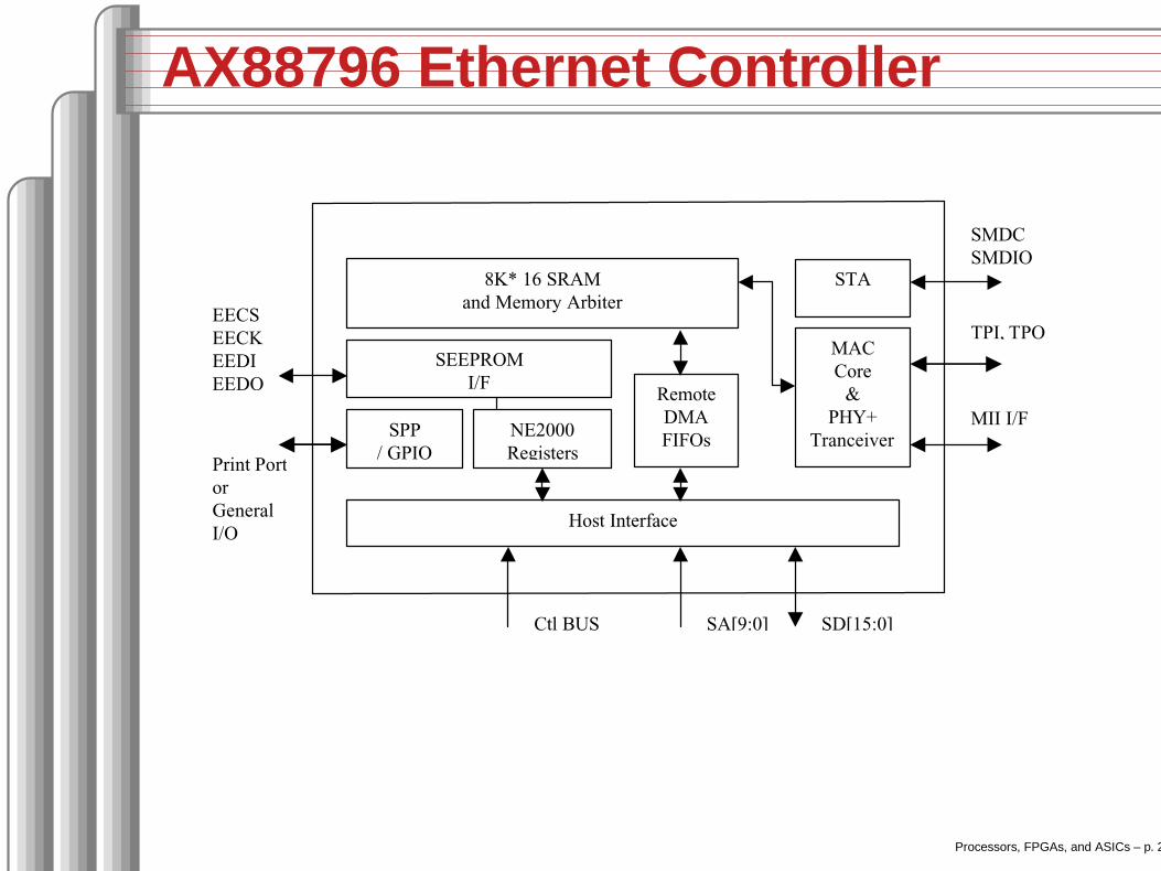
AX88796 Ethernet Controller
Local Bus Fast Ethernet Controller
MAC
Core
&
PHY+
Tranceiver
8K* 16 SRAM
and Memory Arbiter
Remote
DMA
FIFOs NE2000
Registers
Host Interface
STA
SEEPROM
I/F
SD[15:0] SA[9:0] Ctl BUS
MII I/F
EECS
EECK
EEDI
EEDO
TPI, TPO
SPP
/ GPIO Print Port
or
General
I/O
SMDC
SMDIO
Processors, FPGAs, and ASICs – p. 29

Ethernet Controller Registers
Local Bus Fast Ethernet Controller
PAGE 0 (PS1=0,PS0=0)
OFFSET READ WRITE
00H Command Register
( CR )
Command Register
( CR )
01H Page Start Register
( PSTART )
Page Start Register
( PSTART )
02H Page Stop Register
( PSTOP )
Page Stop Register
( PSTOP )
03H Boundary Pointer
( BNRY )
Boundary Pointer
( BNRY )
04H Transmit Status Register
( TSR )
Transmit Page Start Address
( TPSR )
05H Number of Collisions Register
( NCR )
Transmit Byte Count Register 0
( TBCR0 )
06H Current Page Register
( CPR )
Transmit Byte Count Register 1
( TBCR1 )
07H Interrupt Status Register
( ISR )
Interrupt Status Register
( ISR )
08H Current Remote DMA Address 0
( CRDA0 )
Remote Start Address Register 0
( RSAR0 )
09H Current Remote DMA Address 1
( CRDA1 )
Remote Start Address Register 1
( RSAR1 )
0AH Reserved Remote Byte Count 0
( RBCR0 )
0BH Reserved Remote Byte Count 1
( RBCR1 )
0CH Receive Status Register
( RSR )
Receive Configuration Register
( RCR )
Processors, FPGAs, and ASICs – p. 30

Philips SAA7114H Video Decoder
Processors, FPGAs, and ASICs – p. 31

SAA7114H Registers, page 1 of 7 (!)
Processors, FPGAs, and ASICs – p. 32

Fixed-function: The 7400 series
handbook, halfpage
MNA212
1Y1A
31B
1
2
2Y2A
62B
4
5
3Y3A
83B
9
10
4Y4A
114B
12
13Q0
D0
CP
OE
Q1
D1
Q2
D2
Q3
D3
Q4
D4
Q5
D5
Q6
D6
Q7
D7
D
CP Q
D
CP Q
D
CP Q
D
CP Q
D
CP Q
D
CP Q
D
CP Q
D
CP Q
7400 74374Quad NAND Gate Octal D Flip-Flop
Processors, FPGAs, and ASICs – p. 33