printed electrolyte-gated transistors and circuits for
TRANSCRIPT

Printed Electrolyte-Gated Transistors and Circuits
for Flexible Electronics
A DISSERTATION
SUBMITTED TO THE FACULTY OF THE GRADUATE SCHOOL
OF THE UNIVERSITY OF MINNESOTA
BY
Mingjing Ha
IN PARTIAL FULFILLMENT OF THE REQUIREMENTS
FOR THE DEGREE OF
DOCTOR OF PHILOSOPHY
Advisor: C. Daniel Frisbie
April, 2013

© Mingjing Ha, 2013

i
Acknowledgements
First of all, I would like to sincerely thank my advisor, Prof. Dan Frisbie, for his
inspiration, guidance and support throughout my PhD research. I greatly appreciate his
encouragement every time when I’m facing challenges; his ideas and suggestions which
lead to every breakthrough of my projects; and his patience and understanding through all
the time. Without these, this thesis would not be possible. His knowledge, enthusiasms
and dedications to research and education have influenced me deeply. The four and half
years working with him become a great journey for me.
I also would like to express my great gratitude to many people who have helped me on
my thesis research. I thank Prof. Chris Kim and Dr. Wei Zhang for the helpful
discussions and collaborations on circuit design and modeling; Prof. Mark Hersam, Dr.
Alexander Green and other group members (Northwestern University) for the discussions
and collaborations on carbon nanotubes studies; Prof. Chris Leighton, Dr. Mike Manno
and Dr. Shun Wang for the help and valuable discussions on the study of transport
mechanisms in polymer semiconductors; Prof. Russell Holmes, Dr. Kaiyuan Cheng, Dr.
Richa Pandey for discussions on optical characterizations on my devices and assisting on
the instruments; Dr. Mike Renn for teaching me all the knowledge about aerosol jet
printing, and the tremendous support for allowing me use all the tools in his lab for more
than two years.
I thank all of my colleagues in Frisbie group for the helpful, inspiring discussions,
sharing their research experiences, and all the assistance on my experiments, Dr. Yu Xia,
Dr. Jeongho Cho, Dr. Jiyoul Lee and Wei Xie on device fabrications and
characterizations; Dr. Vivek Kalihari, Dr. Dave Ellison, Yanfei Wu on AFM
characterizations; Dr. Sipei Zhang, Dr. Keun Hyung Lee and Dr. Bryan Paulsen for
discussions on electrolyte and polymer synthesis; Dr. Moon Sung Kang, Salil Bapat, Dr.
Bryan Boudouris, Dr. Yan Liang, Dr. Liang Luo, Dr. Daniele Braga, and all the former
and present Frisbie group members for their help and support. I also would like to thank
Prof. Yoshihiro Iwasa and his group (Tohoku University), Optomec. Inc., Soligie, Inc.,

ii
and NanoC, Inc., for the great collaboration experiences. I thank all my friends who made
my years in Minnesota an enjoyable memory.
Last but not the least, I thank my parents, Guiyun Sun and Chongxi Ha, for their
support and trust through all these years. I thank my husband, Yuanpeng Li for being
there all the time. Every single achievement in my life belongs to them too.

iii
To my mother, father and husband.

iv
Abstract
Printed electronics has broad potential applications due to its low fabrication cost,
compatibility with flexible substrates, and its suitability for applications where large
footprints are required. However, the supply voltages of printed circuits are high in
general due to limitations of both the electronic properties of printable materials and the
coarse dimensions of printed transistors. This thesis aims to demonstrate low-voltage
operation of printed circuits by employing a printable electrolyte, a so-called ion gel, with
very large specific capacitance (on the order of F/cm2) as the gate insulator. Ion gels are
composites formed by the self-assembly of triblock copolymers, e.g. poly(styrene-b-
methyl methacrylate-b-styrene) (PS-PMMA-PS), in an ionic liquid, e.g. 1-ethyl-3-
methylimidazolium bis(trifluoromethylsulfonyl)amide ([EMI][TFSA]). These ion gels
and other functional materials, such as semiconductors and conductive polymers were
fabricated by aerosol jet printing to form electrolyte-gated transistors (EGTs) and circuits
on plastic substrates. This thesis demonstrates that these printed devices can achieve low-
voltage operation, fast switching speed, remarkable operational stability, and can realize
electronic functions of logic gates, capacitor, electrochromic device, etc.
To explore the trade-off between supply voltage and switching speed, this thesis
studied EGTs consisted of high capacitance ion gel and high mobility carbon nanotubes
(CNTs), which together enable the fast switching speed at low voltages. The CNT EGTs
were ambipolar and could be used to make complimentary-like inverters and circuits.
Five-stage ring oscillators printed on flexible substrate achieved above 2 kHz frequency,

v
corresponding to less than 50 s delay time. The impact of key parameters on delay times
were studied, including the EGT channel length, ionic conductivity of the ion gel,
parasitic capacitance and resistance. With these understandings, the architecture of EGT
was optimized, and ring oscillators with stage delay as short as 1.2 s time was
successfully demonstrated at voltages < 3 V. These results represent a significant
improvement in the performance of printed electronics. Fabrication and characterization
of inverters and NAND gates, device operational stability and power consumption were
also discussed.
To demonstrate integration of EGTs, a flexible circuit with 23 EGTs, 12 capacitors, 20
resistors and an electrochromic (EC) display pixel operates at a voltage as low as 1 V was
fabricated on plastic substrates. All of the key components were aerosol jet printed from
liquid inks, such as the ion gel, poly (3-hexylthiophene) (P3HT), a semiconductor, and
the conductive polymer, poly(3,4-ethylenedioxythiophene):poly(styrenesulfonate)
(PEDOT:PSS). Characteristics and operation mechanisms of each device were discussed
respectively. The circuit operated continuously for 100 min with no degradation. Overall,
this thesis demonstrates that high reproducibility of device fabrication is possible and that
EGTs may be used to achieve conventional electronic function at low voltage on plastics.

vi
Table of Contents
Table of Contents .......................................................................................................... vi
List of Tables................................................................................................................. ix
List of Figures ................................................................................................................ x
Introduction ................................................................................................... 1 Chapter 1
1.1 Motivation ............................................................................................................ 1
1.2 Review of the Thesis ............................................................................................ 5
Organic Thin Film Transistors and Applications.......................................... 8 Chapter 2
2.1 Charge Transport in Organic Semiconductors ..................................................... 9
2.1.1 HOMO and LUMO Energy Levels ........................................................... 9
2.1.2 Electron-lattice Interaction and Polarons ................................................ 12
2.1.3 Models of Charge Carrier Transport: Band vs. Hopping ........................ 14
2.2 Organic Thin Film Transistors (OTFTs) ............................................................ 19
2.2.1 Operation Mechanism ............................................................................. 19
2.2.2 Characteristics of OTFT .......................................................................... 22
2.3 Electrolyte-Gated Transistors (EGTs)................................................................ 25
2.3.1 Introduction of Electrolyte ...................................................................... 25
2.3.2 Operation Mechanisms of EGTs ............................................................. 28
2.3.3 Applications of EGTs. ............................................................................. 30
2.3.4 Electrochromic (EC) Displays. ............................................................... 32
Carbon Nanotube Transistors and Applications ......................................... 34 Chapter 3
3.1 Introduction ........................................................................................................ 34
3.2 Structures and Characteristics of Carbon Nanotubes ......................................... 34
3.2.1 Structures of Carbon Nanotubes ............................................................. 35
3.2.2 Electronic Properties of Carbon Nanotubes ............................................ 37
3.2.3 Deposition of Carbon Nanotubes ............................................................ 40
3.2.4 Purification of CNTs ............................................................................... 45
3.2.5 CNT Network .......................................................................................... 47

vii
3.3 Electronic Devices Based on CNTs ................................................................... 48
3.3.1 Thin Film Transistors Based on CNTs .................................................... 49
3.3.2 Scaling of CNT FETs .............................................................................. 52
3.3.3 CNT Circuits and Other Applications ..................................................... 54
Printed and Flexible Circuits and Applications .......................................... 58 Chapter 4
4.1 Introduction ........................................................................................................ 58
4.2 Fabrication of Flexible Circuits ......................................................................... 59
4.2.1 Deposition Methods from Gas-phase ...................................................... 59
4.2.2 Transfer-printing ..................................................................................... 62
4.2.3 Deposition Methods from Liquid-phase ................................................. 64
4.3 Printing Techniques for Electronics ................................................................... 65
4.4 Performance and Applications of Flexible and Printed Circuits ........................ 70
4.4.1 Operation Speed of Flexible and Printed Circuits ................................... 70
4.4.2 Complimentary Circuits: Low Power Operation .................................... 73
4.4.3 Other Applications: Displays, RFID, and Sensors .................................. 74
Printed Flexible Electrolyte-gated CNT Transistors and Digital Circuits .. 78 Chapter 5
5.1 Introduction ........................................................................................................ 78
5.2 Printed Electrolyte-gated Ambipolar CNT EGTs .............................................. 79
5.2.1 Device Architecture................................................................................. 79
5.2.2 CNT EGT Performance ........................................................................... 81
5.2.3 Reproducibility of Printed CNT EGTs.................................................... 82
5.3 Inverters Based on Printed CNT EGTs .............................................................. 85
5.3.1 Electrical Characterizations..................................................................... 85
5.3.2 Operational Stability of Printed CNT Inverters ...................................... 87
5.4 Ring Oscillator ................................................................................................... 89
5.4.1 Electrical Characterizations..................................................................... 89
5.4.2 Operational Stability of Printed CNT Ring Oscillators .......................... 91
5.5 Parasitic Capacitance ......................................................................................... 92
5.5.1 Estimation of Parasitic Capacitance and Parasitic Resistance ................ 92

viii
5.5.2 Reduction of Parasitic Capacitance ......................................................... 94
5.6 NAND Gate Based on Printed CNT Transistors................................................ 95
5.7 Conclusions ........................................................................................................ 97
Printed Fast Electrolyte-gated CNT Ring Oscillators ................................. 98 Chapter 6
6.1 Introduction: ....................................................................................................... 98
6.2 Printed CNT EGTs and Inverters ....................................................................... 99
6.2.1 Printed CNT EGTs with Reduced Channel Lengths ............................... 99
6.2.2 Transistor Performance with Various VD .............................................. 102
6.2.3 Printed CNT Inverters with Reduced Channel Lengths ........................ 103
6.2.4 Switching Time of Inverters .................................................................. 106
6.3 Ring Oscillator Performance with Optimized Circuit Parameters ................... 110
6.4 Parasitic Resistance of Printed Gate Electrode ................................................ 113
6.5 Conclusions ...................................................................................................... 116
Printed Flexible Circuit with Integrated Electrochromic Pixel ................. 118 Chapter 7
7.1 Introduction ...................................................................................................... 118
7.2 Device Fabrication and Characterization ......................................................... 119
7.2.1 Circuit Diagram and Design .................................................................. 119
7.2.2 Printed EGTs ......................................................................................... 123
7.2.3 Printed Capacitors ................................................................................. 127
7.2.4 Printed EC Pixel .................................................................................... 132
7.2.5 Printed Resistors and Crossovers .......................................................... 136
7.3 Printed Circuit Performance ............................................................................. 138
7.4 Conclusions ...................................................................................................... 143
Future Research ........................................................................................ 145 Chapter 8
8.1 Power Consumption of Printed Circuits .......................................................... 145
8.1.1 Modification of the Electrolyte Material. .............................................. 149
8.1.2 Modification of Semiconducting CNTs. ............................................... 150
8.2 Capacitor with Large Capacitance and Its Applications .................................. 151
References .................................................................................................................. 154

ix
List of Tables
Table 4.1 Comparison of common printing techniques. .................................................. 66 Table 5.1 Key parameters of transistors printed on flexible polyimide and on SiO2
substrates ................................................................................................................... 83

x
List of Figures
Figure 2.1 A schematic of and Bonds. The blue lines are bonds and the yellow
clouds are bonds. ................................................................................................... 10 Figure 2.2 The bonding-antibonding interaction between the HOMO and LUMO levels.
................................................................................................................................... 11 Figure 2.3 Band and Hopping Transport. ........................................................................ 13 Figure 2.4 A schematic of positive charge induced polaron. ........................................... 14
Figure 2.5 Energy band and band gap.. ............................................................................ 16
Figure 2.6 Mott variable range hopping........................................................................... 18 Figure 2.7 Architectures of thin film transistors. ............................................................. 20
Figure 2.8 Operation mechanism of p-type OTFT. ......................................................... 21 Figure 2.9 Transfer and output characteristics of an OTFT. ............................................ 23 Figure 2.10 Chemical structure of solid polymer electrolyte........................................... 26 Figure 2.11 Chemical structures of common ionic liquids and polymers for ion gel. ..... 27
Figure 2.12 Operation mechanism of EGT. ..................................................................... 29 Figure 2.13 Printed electrochemical circuits and sensors. ............................................... 31
Figure 2.14 Printed ion gel gated transistors and circuits. ............................................... 32 Figure 2.15 Active matrix of printed electrochromic displays. ....................................... 33 Figure 3.1 Atomic structure of graphene, graphite, carbon nanotube and Fullerene (C60).
................................................................................................................................... 35
Figure 3.2 Structure of CNTs. .......................................................................................... 37 Figure 3.3 Metallic and semiconducting CNTs. .............................................................. 39 Figure 3.4 Band gap versus radius for zigzag CNTs. ...................................................... 40
Figure 3.5 SEM/AFM images of CNT films grown by various methods. ....................... 42 Figure 3.6 Deposition methods of CNTs. ........................................................................ 44
Figure 3.7 Suspension and purifications of CNTs. .......................................................... 47 Figure 3.8 Mobility and ON/OFF ratio trend and comparisons for nano-transistors. ..... 49 Figure 3.9 FETs based on CNTs. ..................................................................................... 50
Figure 3.10 Ambipolar transportation of FET based on CNTs. ....................................... 51 Figure 3.11 Mobility and ON/OFF ratio of CNT network. ............................................. 54
Figure 3.12 A 5-stage ring oscillator fabricated on a single CNT. .................................. 55 Figure 4.1 Flexible OTFTs based on Pentacene. ............................................................. 61 Figure 4.2 Schematic process flow of single-crystal silicon ribbon fabrication. ............. 63 Figure 4.3 Ring oscillators based on ribbon of silicons. .................................................. 63 Figure 4.4 Common printing process. .............................................................................. 67
Figure 4.5 Ink-jet printing mechanism. ............................................................................ 68 Figure 4.6 Scheme of aerosol jet printing. ....................................................................... 69 Figure 4.7 Circuit diagram of a typical ring oscillator and its output. ............................. 71 Figure 4.8 Stage delay time of ring oscillators. ............................................................... 72 Figure 4.9 Flexible RFID tags.......................................................................................... 75
Figure 4.10 Flexible sensors. ........................................................................................... 76

xi
Figure 5.1 Device architecture of printed ion gel-gated CNT transistors. ....................... 80 Figure 5.2 Electrical characterization of ion gel gated CNT EGTs showing ambipolar
transport. ................................................................................................................... 82 Figure 5.3 Distribution of the key parameters of printed ambipolar CNT EGTs on
polyimide substrates. ................................................................................................. 84
Figure 5.4 Distribution of the key parameters of the printed ambipolar CNT EGTs on
SiO2 substrates. ......................................................................................................... 84 Figure 5.5 Electrical characterization of printed complementary-like inverters based on
ambipolar ion gel gated CNT transistors. ................................................................. 86 Figure 5.6 Dynamic responses of the CNT inverters. ...................................................... 87
Figure 5.7 Stability of the printed CNT inverter on polyimide substrate. ....................... 88 Figure 5.8 Five-stage ion gel gated complementary-like CNT ring oscillator with output
buffer. ........................................................................................................................ 90 Figure 5.9 Time stability of a CNT ring oscillator printed on polyimide substrate. ........ 91 Figure 5.10 Estimation of the parasitic capacitance. ....................................................... 93 Figure 5.11 Reduction of the parasitic capacitance.. ....................................................... 94
Figure 5.12 AFM images of Au electrodes. ..................................................................... 95 Figure 5.13 NAND logic gate based on ion gel gated printed CNT transistors. ............. 96
Figure 6.1 Performance of ion gel gated ambipolar CNT EGTs. .................................. 100 Figure 6.2 Transfer curves of an CNT EGT with various drain biases, from −0.01 V to
−1 V. ....................................................................................................................... 103 Figure 6.3 Performance of an ion gel gated CNT inverter. ............................................ 104
Figure 6.4 Parameters affecting the frequency and switching time of the CNT inverters.
................................................................................................................................. 108 Figure 6.5 Circuit diagram and optical images of ring oscillator. ................................. 110
Figure 6.6 Circuit performance of fast printed 5 stage ring oscillator. .......................... 112 Figure 6.7 Fast printed ion gel-gated CNT ring oscillator with 83 kHz output frequency,
at VDD=2.2 V. .......................................................................................................... 113 Figure 6.8 Effects of electrode material on frequency response of printed capacitor. .. 115 Figure 7.1 Printed, flexible circuit and electrochromic pixel based on ion gel and P3HT.
................................................................................................................................. 121
Figure 7.2 Diagram of printed circuit. ........................................................................... 122 Figure 7.3 Printed ion gel gated P3HT EGTs. ............................................................... 125 Figure 7.4 Printed ion gel/P3HT capacitors. .................................................................. 127 Figure 7.5 Electrical characteristics of printed capacitor. .............................................. 129 Figure 7.6 Displacement current of capacitors with and without P3HT layer. .............. 130
Figure 7.7 Impact on delay time and effective capacitance of printed capacitors. ........ 131 Figure 7.8 Printed EC pixel............................................................................................ 134 Figure 7.9 Dynamic optical response of the printed EC pixel under 1 Hz bias. ............ 135 Figure 7.10 I-V characteristics of printed resistor and crossovers. ................................ 137 Figure 7.11 Inverter and signal flow in delay chains.. ................................................... 138
Figure 7.12 Output of NAND 3. .................................................................................... 140
Figure 7.13 The output performance of the printed circuit. ........................................... 141

xii
Figure 7.14 Capacity of the driving circuit. ................................................................... 142 Figure 7.15 Operational stability of printed circuit. ....................................................... 143 Figure 8.1 The simulations of the ambipolar CNT EGTs and inverters. ....................... 148 Figure 8.2 Transfer characteristics of transistors based on CNTs with different diameters.
................................................................................................................................. 150
Figure 8.3 A 8x8 DRAM array based on printed ion gel-gated transistors. .................. 152
Chapter 1. Introduction
1
Introduction Chapter 1
1.1 Motivation
Microelectronics based on silicon crystals and compound semiconductors has had
significant impacts on technology over the last half century. The circuit performance and
integration density continuously increase due to the scale-down of device dimensions.
However, challenges remain in certain areas, e.g., the integration of electronics onto
flexible plastic, paper, or metal substrates. Envisioned applications of flexible electronics
include roll-up displays, wearable energy-harvesting system, electronic sensors for robots
(e-skins), sensors for biological system (bionic ears), etc. Fabrication of conventional
electronics, which usually requires high temperatures up to several hundreds of degrees
(ion implantation, contact annealing, etc.), is incompatible with most flexible substrates.
Furthermore, many process steps in conventional semiconductor industry are intrinsically
difficult to be adapted to large-area fabrications, as required for the large area displays,
such as photolithography and vacuum deposition processes.
Amorphous silicon was first studied to address these challenges, especially for the
large-area applications, but the process temperatures are still relatively high (> 200 °C)
and not compatible with most plastic substrates. Some groups have demonstrated flexible
circuits based on very thin silicon stripes transferred to flexible substrates using state-of-
art fabrication techniques (transfer printing or pick-and-place methods),1 and these Si
based circuits benefit from superior electronic properties.

Chapter 1. Introduction
2
Organic materials, including semiconducting, insulating and conductive materials,
have received intensive attention because they are naturally flexible and compatible with
low-temperature, low-cost (solution processable) fabrication. Over the last few decades,
organic thin film transistor (OTFT) backplane of active matrix liquid crystal displays
(AMLCDs) and active matrix organic light-emitting diodes (AMOLEDs) were reported
by many research groups and companies.2-4
OTFTs fabricated on flexible substrates were
also demonstrated in applications such as e-skins, large area sensors, disposable sensor
tapes, radio-frequency identification (RFID) tags, and smart objects.5-15
The technologies
used in these flexible electronics are still mostly conventional evaporation and
photolithography. Although they are adaptable to flexible substrates, low-cost and large
area fabrication is still challenging.
An alternative option for achieving flexible electronics is to employ graphic arts
methods such as flexographic, gravure or ink jet printing to pattern metallic,
semiconducting, and insulating inks onto foils and paper.16-21
Liquid phase printing offers
the potential for high throughput roll-to-roll (R2R) or sheet-to-sheet processing of
electronics on large area substrates. In addition, additive printing from functional liquid
inks is promising for cost-effective electronics, such as disposable or portable
applications. For example, a flexible, all printed, 1-bit RFID tag was demonstrated
recently by mass-printing techniques with estimated cost of 3 cents.9
Of the many technical challenges facing printed electronics, one of the most
fundamental is the trade-off between supply voltage and operating speed, which is not
only limited by the intrinsic material properties, but also the device architecture and

Chapter 1. Introduction
3
dimensions. Organic semiconductors generally have relatively low mobilities compared
to conventional semiconductors, and transistors based on which often require operation
voltage > 10 V. The printed transistors require even higher voltage (tens of volts), due to
the limitations of printing resolution and large source-to-drain channel. The large
voltages are not practical for many potential applications of flexible electronics where
power will be supplied by thin film batteries or radio-frequency fields. Meanwhile, the
operation speed of the printed circuit is also much lower. The typical delay time in
organic circuits is on the order of 10 s, while in printed circuits is generally around ms.
A barrier to low voltage printed electronics is the low capacitance of many printed
gate dielectrics (i.e., the printed gate dielectric layers are too thick and their dielectric
constants are too small), which necessitates larger gate voltages to switch the transistors.
Many groups explored different strategies to address this issue, including using
dielectrics with high , very thin dielectric layer (such as self-assembled monolayer), and
electrolyte, and successfully reduced the operational voltages.22-27
Another direction to
improve the performance of printed circuits is to employ high mobility semiconductors.
Some groups are investigating transfer printing1,28-32
or jet printing9,33-38
of high mobility
semiconductors, e.g., silicon, oxides, nanowires, graphene and carbon nanotubes (CNTs),
and these efforts have the potential to produce low voltage circuits operating at high
speed.
This thesis combines both strategies, by employing high mobility carbon nanotubes
and high capacitance electrolyte ion gel, and demonstrates printed, flexible circuits which

Chapter 1. Introduction
4
achieve both low supply voltage and high speed. Both CNT and ion gel were patterned by
aerosol jet printing of liquid inks. Ion gel-gated CNT thin film transistors (TFTs) with 50
m channel lengths display ambipolar transport with both electron and hole mobilities >
20 cm2/Vs; these devices form the basis of printed inverters, NAND gates, and ring
oscillators on both polyimide and SiO2 substrates. Five-stage ring oscillators achieve
frequencies > 2 kHz at supply voltages of 2.5 V, corresponding to stage delay times of 50
s. The data was first reported on ACS Nano, 2011, which represented a substantial
improvement for printed circuitry fabricated from functional liquid inks.
In order to understand the limitations of the operation speed in electrolyte-gated
transistors and circuits, and further improve the circuit performance, the impacts of
device architecture and materials properties are studied. The inverter delay time decreases
as the channel length scaling down. And the ionic conductivities of ion gel also have a
strong effect on the delay time. The higher the ionic conductivity the gel has, the faster
the transistor can switch. With these understandings, an 83 kHz ring oscillator (with stage
delay time ~ 1.2 s) is successfully demonstrated, based on transistors with 5 m channel
length. The result is published in Nano Letters, 2013. With further optimization of device
architecture, achieving 1 MHz printed ring oscillators is possible.
Furthermore, this thesis explores the applications of electrolyte-gated devices. The
printed electrolyte-gated polymer OTFTs has been demonstrated by our group
previously.24,25
With similar materials and architecture, electrolyte-gated capacitors and
electrochromic (EC) display pixels are fabricated by printing as well. All of components

Chapter 1. Introduction
5
are printed on a PET substrate to form a driving circuit integrated with EC display.
Characteristics of each component are studied. The circuit can operate at a voltage as low
as 1 V, and output a large current which is high enough to switch the mm2 size EC
display pixel. The novelty of this work lies in (1) the use of aerosol jet printing to
produce a functional circuit containing 68 individual devices (e.g., transistors, capacitors,
resistors, etc.) with good reproducibilities, (2) the integration of a printed EC pixel onto
the same substrate using the same printing methodology, and (3) the very low voltage
operation of the complete assembly.
1.2 Review of the Thesis
Chapter 2 introduces the theories of charge carrier transport in organic
semiconductors, the architecture and operation mechanism of organic thin film
transistors. In addition, the operation mechanism and characteristics of electrolyte-gated
transistors (EGTs) are discussed. Applications of electrolytes in flexible electronics are
reviewed.
Chapter 3 briefly introduces the structure and electronic properties of carbon
nanotubes, as well as the common growth and fabrication methods. The electronic
devices based on the carbon nanotubes are reviewed additionally.
Chapter 4 focuses on the fabrication of flexible and printed electronics. First, common
methods of fabricating flexible transistors and circuits are introduced. The printing
methods are reviewed in details in an individual section. The last section summarizes the
circuit performances of organic circuits and printed circuits, i.e. the delay time vs. supply

Chapter 1. Introduction
6
voltage, which is one of the major focuses of this thesis. Research in complementary
circuits and other applications, such as displays and RFIDs, are also reviewed.
Chapter 5 shows the study on printed, flexible circuits based on electrolyte-gated CNT
transistors. Following with the introduction of fabrication method and characteristics of
transistors, the performances of digital circuits, including inverters, NAND gate, and ring
oscillators are discussed. The parasitic capacitance and operation stability of the circuits
are studied in addition. These results have been published as “Printed, Sub-3V Digital
Circuits on Plastic from Aqueous Carbon Nanotube Inks”, M. Ha, Y. Xia, A. A. Green,
W. Zhang, M. J. Renn, C. H. Kim, M. C. Hersam and C. D. Frisbie, ACS Nano, 4, 8,
4388-4395.
Chapter 6 discusses the factors that affect the speed of the electrolyte-gated CNT
circuits, and how to further improve the circuit performance. The effects of scaling down
the transistor dimension and electrode dimension are demonstrated. The output
characteristics of inverter based on the ambipolar transistors are discussed. The stage
delay time of inverters are characterized with various channel lengths, and the ionic
conductivities of electrolytes. Ring oscillators with delay time less than 5 s were
demonstrated. These results have been published as “Aerosol Jet Printed, Low Voltage,
Electrolyte Gated Carbon Nanotube Ring Oscillators with Sub-5 μs Stage Delays”, M.
Ha, J. T. Seo, P. L. Prabhumirashi, W. Zhang, M. L. Geier, M. J. Renn, C. H. Kim, M. C.
Hersam, and C. D. Frisbie, Nano Letters, 13, 3, 954–960 (2013)

Chapter 1. Introduction
7
Chapter 7 summarizes the studies on applications of electrolyte-gated devices,
including transistors, capacitors and EC displays. Characteristics of each component are
discussed respectively. All components are integrated on a PET substrate and can switch
a mm2 size EC pixel at 1 V. The circuit performance and stability are discussed. These
results are in preparation for submission as “Aerosol Jet Printed, 1-Volt Drive Circuit on
Plastic with Integrated Electrochromic Pixel”.
Chapter 8 discusses the future research directions of printed circuits. The power
consumption issue of ambipolar circuits is discussed, with proposals of how to reduce the
power consumption and some preliminary data. In addition, other applications of printed
devices are discussed. In particular, a memory array based on printed capacitors based on
electrolyte and polymer semiconductors is demonstrated, which results have been
published as “A 1V printed organic DRAM cell based on ion-gel gated transistors with a
sub-10nW-per-cell Refresh Power”, W. Zhang, M. Ha, D. Braga, M. J. Renn, C. D.
Frisbie and C. H. Kim, Solid-State Circuits Conference Digest of Technical Papers
(ISSCC), 2011 IEEE International, 326-328, (2011)

Chapter 2. Organic Thin Film Transistors and Applications
8
Organic Thin Film Transistors and Chapter 2
Applications
The organic semiconductors include carbon-based small molecules and polymers.
Studies of these materials date back to early 20th
century,39
and the distinct electronic and
optical properties of organic molecules attracted many researchers since then.40-42
In
1977, the discovery of the charge transport in conjugated polymers opened up new
research directions in this field. Alan Heeger, Hideki Shirakawa, Alan McDiarmid were
awarded the Nobel Prize in Chemistry, 2000, for this work.43
Organic materials also offer
vast opportunities of tuning their electronic and optical properties by molecular
engineering. In addition, they are naturally flexible and compatible to solution process or
low-temperature fabrication, which makes them very attractive candidates for flexible
electronics. Many promising progress has been demonstrated in flexible electronics over
the past decades.
This chapter starts with introducing the charge carrier transport theories in organic
semiconductors. Then, the architecture and operation mechanism of the organic field
effect transistor (OFET), the basic building block of organic circuits, is discussed. In
addition, a unique type of transistors, electrolyte-gated transistor (EGT) is also discussed.

Chapter 2. Organic Thin Film Transistors and Applications
9
2.1 Charge Transport in Organic Semiconductors
Due to the large size of the molecule and long intermolecular distance in organic
semiconductors, the forces between molecules are weaker than the covalent bonds in
inorganic semiconductors. In organic semiconductors, the conduction bands are narrower,
the charge transfer is not as efficient, thus the charge carrier mobility is lower. For
example, the hole mobility of rubrene single crystal can be up to 20 cm2/Vs,
44 which is
among the highest mobilities of organic semiconductors. However, this is still orders of
magnitude lower than the mobility of typical doped silicon which is around 103 cm
2/Vs.
To understand this difference, this section discusses the theories of charge transport in
organic semiconductors. The formation of energy levels, the concept of band-like
transport, polarons and phonon-assisted hopping, the nearest-neighbor hopping and
variable range hopping (VRH) models are reviewed.
2.1.1 HOMO and LUMO Energy Levels
Conjugated organic semiconductors are compounds consisting of sp2
hybridized
carbon atoms. The hybridization of orbitals 2s, 2px and 2py creates three bonds, which
link a carbon atom to its neighbors. The remaining 2pz orbital forms a bond. The
orbitals lie above and below the plane of carbon atoms and have significantly less overlap
than the orbitals. Figure 2.1 shows the atomic orbital (left), the lowest energy of
molecular orbitals (right above), and delocalized orbitals (right bottom) of a benzene
molecule. The positive and negative signs represent the two phases of the orbital. Since

Chapter 2. Organic Thin Film Transistors and Applications
10
the bond is weaker than bond, the delocalized electrons can transport in these
states. The conjugated organic materials thus can be conductive or semiconducting.
Using the linear combination of atomic orbitals (LCAO) theory, one can calculate the
wavefunction of the -electron in bonding and anti-bonding states, respectively. The
bonding states have lower energy than the anti-bonding states, therefore they are
energetically favored. In organic materials, the bonding and anti-bonding states are
referred as highest occupied molecular orbital (HOMO) and lowest unoccupied molecular
orbital (LUMO). The HOMO and LUMO levels of an isolated ethylene molecule are
shown in Figure 2.2 (left). When two ethylene molecules are brought to each other in a
cofacial configuration, the LUMO level and the HOMO level will split due to the
interactions between states Figure 2.2 (middle). A large number of ethylene molecules
stacking closely will result further splitting and eventually create the LUMO and HOMO
band, as shown in Figure 2.2 (right).
Figure 2.1 A schematic of and Bonds. The blue lines are bonds and the yellow
clouds are bonds.

Chapter 2. Organic Thin Film Transistors and Applications
11
The width of the splitting energy levels is in proportion to the transfer integrals:
∑ ∫ ( ) ( ) (2.1)
where is the wavefunction of an electron, and H is the Hamiltonian which describes the
electron-lattice interaction. Equation 2.1 indicates a strong electron-lattice interaction will
result in large transfer integrals, thus wider bands. For example, in silicon crystal, the
strong covalent bonds lead to a band width of approximately 12 eV. However, the
intermolecular force in organic materials is much weaker and the width of energy bands
in organic semiconductors is only around 1 eV.
Figure 2.2 The bonding-antibonding interaction between the HOMO and LUMO
levels.45

Chapter 2. Organic Thin Film Transistors and Applications
12
2.1.2 Electron-lattice Interaction and Polarons
The transport mechanism is usually divided into two regimes: band-like and hopping
transport. Generally, the electron-lattice coupling strength determines which mechanism
is dominant. A quantitative analysis suggested by Kao and Hwang compares the electron
relaxation time , the intermolecular vibration period and the intramolecular vibration
period .46
The vibration periods are typically 10−12
s for intermolecular modes and
10−14
s for intramolecular modes. If , that means the electron motion is
rapid enough so that both vibrations can be ignored or treated as a perturbation. Thus, the
electron can be considered as delocalized, traveling through the lattice as a wave, shown
in Figure 2.3, corresponding to the band transport in section 2.1.3.
The second case is , which indicates that the intramolecular vibration is
faster than the electron motion. In this case, the electron stays on a lattice site long
enough that the molecules have enough time to relax to a new equilibrium position. This
leads to the formation of a polaron. If the spatial extension of a polaron is large compared
to the lattice constant, the polarization of the lattice can be treated as a continuum.47,48
This is Fröhlich polaron, which refers to the long range interactions. If the polaron has
the size on the order of the lattice constant, it is called Holstein polaron, which refers to
the short range interactions.49
The idea of the transport of small polarons was proposed by Yamashita and Kurosawa
in 1950s,50
and developed by Holstein and Emin49,51,52
to describe the conduction of the

Chapter 2. Organic Thin Film Transistors and Applications
13
materials with low mobilities. Silinsh and Capek discussed in details about the
polarization in organic solids.53
Figure 2.3 Band and Hopping Transport. 54
Figure 2.4 illustrated the formation of electric dipoles caused by a positive charge
trapped in a molecule.55
Due to the Coulomb effect, the -electrons of the surrounding
lattice sites are attracted toward the center site where the positive charge sits. The polaron
can also include a lattice deformation effect if the interaction is strong. Since the lattice

Chapter 2. Organic Thin Film Transistors and Applications
14
relaxation is faster than the electron’s motion, one can consider the hole hopping in a way
that the heavy polaron jumps with it, which requires a large activation energy and usually
involves the emission and absorption of multiple phonons. The nature of phonon-assisted
process is shown in Figure 2.3 schematically.
Figure 2.4 A schematic of positive charge induced polaron.55
2.1.3 Models of Charge Carrier Transport: Band vs. Hopping
Band Transport. In solid state physics, band theory has been well established and
employed to explain various materials properties, especially the electronic properties.
Atoms in a highly pure crystalline material (bulk) have long range order of the lattice
structure. The periodic lattice forms periodic potential wells due to the Coulomb
interaction between electrons and ions, in which electrons are only allowed to have
certain states.56
An electron wavepacket is allowed to propagate inside the bands, and

Chapter 2. Organic Thin Film Transistors and Applications
15
forbidden in the band gaps. Energy bands and band gaps can be explained quantitatively
by solving the time independent Schrödinger equation.
An energy band gap on the order of electron volts gives the semiconductor material an
electrical conductivity between those of metal and insulator. In semiconductors, the
intrinsic conductivity and carrier concentrations are mostly controlled by the energy gap,
Eg/kBT. A smaller energy gap will induce higher concentration of intrinsic carriers and
higher conductivity.57
The material property of optical absorption usually gives the value
of the energy gap. The threshold of continuous optical absorption at frequency of
determines the band gap Eg= . Another way to characterize the energy gap
experimentally is to measure the temperature dependence of the conductivity or of the
concentration of the carrier density in the intrinsic range, which can be obtained by the
Hall Effect measurement.
The highest energy band filled with electrons at the absolute zero temperature is called
valence band (HOMO); the energy band lies upon the valence band, where excited
electrons can transport, is called conduction band (LUMO). At a finite temperature above
absolute zero, electrons can be excited by a thermal activation energy and jump into the
conduction band. The empty states they leave behind are called holes, carrying positive
charges. Both electrons and holes are able to move under an applied electric bias thus
create a current. Figure 2.5 shows the allowed electron states calculated by using Kronig-
Penney model.

Chapter 2. Organic Thin Film Transistors and Applications
16
The value of the current generated by the external electric field (E) depends on how
fast the carriers can move. The carrier’s drift velocity can be written as vd= E, where is
the carrier mobility, indicating the velocity of electron’s motion under unit electric field.
This is an important parameter to characterize the performance of many semiconductor
devices. As mentioned in pervious sections, the covalent bond in inorganic
semiconductors has stronger bonding interactions, leading to a larger bandwidth, while
the weak Van der Waals force dominating in organic materials yields smaller bandwidth.
Figure 2.5 Energy band and band gap. A reduced-zone band structure of allowed E-k
states in a 1-D crystal with N atoms (Kronig-Penney model).56
Miller-Abrahams Hopping. When the bonding interactions are so weak that the
electrons may not be considered as delocalized, the band model does not apply. In this

Chapter 2. Organic Thin Film Transistors and Applications
17
case, the charge carrier has to transport in a thermally activated hopping behavior.58,59
Miller-Abrahams hopping model, which is also called nearest-neighbor hopping,
assumes that the localization is strong so the overlap of the electrons wavefunctions fall
rapidly with distance. Thus the electron can only jump to the nearest state in space.60
Mott defined the rate at which the wavefunction on a single well fell off with the distance
as exp(-2 r), where =√ is the inverse localization length of the wavefunction.
The nearest-neighbor hopping happens when R0 1, where R0 is the average distance to
a nearest neighbor site. Then the hopping probability per unit time is:
(
) (2.2)
where R is the hopping distance, E is the activation energy, F is the applied electric field,
k is the Boltzmann’s constant, and T is the absolute temperature in degree K. For weak
electric field, eRF kT. Thus the mobility of the nearest-neighbor hopping has the
temperature dependence which turns out to be an Arrhenius-like relation:
( ) (2.3)
where is the prefactor, E 1/ N(EF), is usually on the order of 0.1 eVs in organic
amorphous semiconductors. The mobility will decrease with decreasing temperature,
which is distinct from the band-like transport behavior.
Mott Variable Range Hopping (VRH). If R0 is comparable or less than unity, the
overlap of the wavefunction is not limited within the nearest neighbors. At 1968, Mott
was the first to point out that, as the temperature decreases, the hopping distance R
increases and the thermal activation energy decreases.61,62
The electron tends to hop to a

Chapter 2. Organic Thin Film Transistors and Applications
18
state that is energetically favorable, even this requires it to hop over a long spatial
distance. Considering a system with localized states near the Fermi level, as shown in
Figure 2.6, as the temperature decreases, the two relevant states at which the hopping
takes place are limited in a narrower band, with width proportional to T. Therefore the
available states are separated further apart, forcing the electron to hop via a longer
distance. This is called Mott variable range hopping (VRH) model. The term variable
range emphasizes that the hopping distance is not confined to the nearest-neighbors.
Figure 2.6 Mott variable range hopping. The density of sates near the Fermi level is
shown on the right, and the shadow part indicates the occupied states.
Multiple Trapping and Release Model. The multiple trap and release model is a
transport mechanism combining the band-like transport with the hopping process. The
carriers still travel in a continuous energy band, however, the diffusive transport is
limited by shallow traps which lie in the band gap. A trapped carrier has to be thermally
activated in order to hop back into the band, and the carrier is easily to be retrapped by
another trap state. The traps can be structural or chemical in nature, such as vacancies,

Chapter 2. Organic Thin Film Transistors and Applications
19
positional disorderness, dangling bonds and impurities. The initial model was developed
for amorphous silicon film,59
which gave the result similar to the hopping process due to
its thermal activation nature
( ) ( ) (2.4)
where is the trap-free mobility, E is the energy of traps. Horowitz el al. extended this
model to organic materials and considered the gate voltage dependence,63
and obtain a
mobility as a function of VG and temperature
(
)
(2.5)
where is the trap-free mobility, NC is the DOS in the transport band, Nt0 is the total
surface density of traps.
2.2 Organic Thin Film Transistors (OTFTs)
2.2.1 Operation Mechanism
Thin film transistor (TFT) utilizes a capacitively coupled gate dielectric layer to
control the current flowing through the semiconductor layer. Four common architectures
are shown in Figure 2.7. The basic architecture of TFT includes three electrodes (gate,
source and drain), an insulating layer serving as the gate dielectric, and a semiconductor
layer transporting charge carriers. TFTs generally have two different geometries, top
contacts and bottom contacts. The operation mechanisms are the same for both
geometries, although the device performances may be different. For instance, contact
resistances are usually larger in (a) & (d). Also, the insulating layer can be fabricated

Chapter 2. Organic Thin Film Transistors and Applications
20
either on top of the device, which is called top-gate transistor, or on the bottom, which is
called bottom-gate transistor.
The gate electrodes and the insulating layer work as a valve, which can control the
number of charge carriers in the semiconductor layer. Most OTFTs are based on intrinsic
organic semiconductors, meaning that the mobile charge carriers must be injected from
electrodes. Theoretically, the gate bias can induce both electrons and holes in the
semiconductor layer, which will lead to an ambipolar operation. However, unipolar,
especially the p-type transport is often seen in OTFTs.64
Figure 2.7 Architectures of thin film transistors. (a) top contacts with bottom gate
electrode, (b) bottom contacts with bottom gate, (c) top contacts with top gate and (d)
bottom contacts with top gate.55

Chapter 2. Organic Thin Film Transistors and Applications
21
Figure 2.8 Operation mechanism of p-type OTFT. (a) & (b), band diagram of MIS
structure with zero gate bias (VG = 0), and a negative bias (VG < 0), respectively. (c)
Schematic of a OTFT with zero gate bias applied, and (d) with negative gate bias. (e)
Band diagram of the metal contacts and the semiconductor, with zero VG and VD, and
(f) with a negative drain bias.
The operation mechanism of OTFT is explained based on p-type transistor as an
example. A small negative gate bias will induce localized positive charges in
EF
HOMO
LUMO
Metal Organic SemiconductorInsulator Metal Organic SemiconductorInsulator
EF
HOMO
LUMO
VG
InsulatorS D
G
InsulatorS D
G
HOMO
LUMO
EF VD
So
urc
e
So
urc
e
Dra
in
Dra
in
(a) (b)
(c) (d)
(e) (f)
VG=0
VD=0
VG<0
VD<0
VG=0 VG<0
VD=0 VD<0

Chapter 2. Organic Thin Film Transistors and Applications
22
semiconductor at the insulator-semiconductor interface. These localized charges start to
fill the deep traps in the energy gap, which energy level is separated from the top of the
HOMO level by more than a few kBT. As the bias getting more negative and more traps
are filled, the Fermi level, which is initially located between the HOMO and LUMO
level, moves closer to the HOMO band, as shown in Figure 2.8 (b). As soon as (EF-
EHOMO) becomes comparable to kBT, electrons can be thermally excited from the band
into the empty localized states, thus the holes are generated. Therefore, a p-channel is
formed at the insulator-semiconductor interface, as shown in Figure 2.8 (d). A negative
VD allows the holes to be injected from the source contact, flowing across the channel,
and extracted from the drain contact. The conductance of the semiconductor becomes
several orders of magnitude larger when the device is turned ON by the gate bias. As the
gate bias getting more negative, the current flowing across the channel increases due to
the increasing number of charge carriers. Additionally, Figure 2.8 (e) and (f) show the
Fermi level is elevated at the drain side by the source-drain bias, which is the driving
force of carriers flowing across the channel.
2.2.2 Characteristics of OTFT
The performance of a transistor is usually characterized by the transfer and output
characteristics. Tuning the longitudinal electric field by varying the gate bias will change
the transverse drain current, which is shown as a typical transfer curve in Figure 2.9 (a).
On the other hand, with constant gate voltage, varying the drain bias also changes the
drain current, which is the output curve, as shown in Figure 2.9 (b).
Chapter 2. Organic Thin Film Transistors and Applications
23
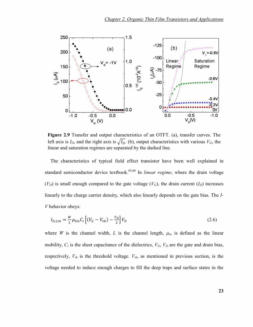
Figure 2.9 Transfer and output characteristics of an OTFT. (a), transfer curves. The
left axis is ID, and the right axis is √ . (b), output characteristics with various VG, the
linear and saturation regimes are separated by the dashed line.
The characteristics of typical field effect transistor have been well explained in
standard semiconductor device textbook.65,66
In linear regime, where the drain voltage
(VD) is small enough compared to the gate voltage (VG), the drain current (ID) increases
linearly to the charge carrier density, which also linearly depends on the gate bias. The I-
V behavior obeys:
[( )
] (2.6)
where W is the channel width, L is the channel length, in is defined as the linear
mobility, Ci is the sheet capacitance of the dielectrics, VG, VD are the gate and drain bias,
respectively, Vth is the threshold voltage. Vth, as mentioned in previous section, is the
voltage needed to induce enough charges to fill the deep traps and surface states in the

Chapter 2. Organic Thin Film Transistors and Applications
24
semiconductor. From the linear plot of ID-VG curve, Vth can be extracted when the
extension line of ID crosses the one of off-current.
If VD is larger than (VG - Vth), the latitudinal electric field becomes comparable to or
larger than the longitudinal electric field, which results in the non-uniform carrier density
along the channel. Close to drain electrode, the carrier density falls to zero, which is
called the pinch-off region. As the drain voltage increases, the pinch-off region expands.
The resistivity of the pinch-off regime is large due to the low carrier density and low
mobility. Therefore, most of the drain voltage drops at this regime. At this stage, the
current no longer increase as VD, which is called the saturation regime, as shown in
Figure 2.9 (b). The real bias drop on the channel is now approximately equal to the gate
voltage, then Eqn. 2.6 becomes
( ) (2.7)
where is the saturation mobility. From Eqn 2.6, the linear mobility can be obtained
from the channel transconductance (gm):
(2.8)
and the saturation mobility can be extracted from the slope of √ versus VG :
√
√
(2.9)
This assumes that the mobility is a constant with VG, which is not always true in
experiments. The observed mobility can either increase with VG, due to the contact

Chapter 2. Organic Thin Film Transistors and Applications
25
resistance dominating when VG is small, or decrease with VG since the distribution of trap
density might increase exponentially as the Fermi level approaching the HOMO level.
2.3 Electrolyte-Gated Transistors (EGTs)
The low mobilities in organic semiconductors are the major limitations of the output
current and switching frequency of OTFTs. One of the strategies to improve the device
performance is to induce more charge carriers in channel by increasing the capacitance of
gate dielectric layer. Some researchers employed ultra-thin dielectric layer (including
self-assemble monolayer) and high- materials.23,67-69
An intriguing direction is to use the
electrolyte as the dielectric layer, which is ionically conducting and electronically
insulating. This section discusses the operation mechanisms of electrolyte-gated
transistors (EGTs) and their applications.
2.3.1 Introduction of Electrolyte
Using electrolyte as the gate dielectric material is not new in this area. The first Ge
transistor was demonstrated with the presence of aqueous electrolyte solutions.70
The
study of EGTs dates back to Wrighton’s work in 1980s, who intensively studied the
electrochemical doping of semiconducting polymers using electrolytes.71-75
Many
research groups now utilize electrolyte as a dielectric layer gating various type of
semiconducting materials to fabricate transistors or study the carrier transport
phenomena.76-79

Chapter 2. Organic Thin Film Transistors and Applications
26
Although the early studies in this area are often based on electrolyte in liquid phase,
the solid state electrolyte is more applicable in electronics applications. The conventional
solid state electrolyte is acquired by dissolving inorganic salts in soft polymers. For
example, lithium salts LiClO4 dissolved in poly(ethylene oxide) (PEO) (Figure 2.10), was
used to gate various semiconductors, including organic single crystals, small molecules,
polymers and carbon nanotubes.79-83
In this electrolyte, the PEO polymer chain is flexible
so that the Li+ cation can move along the chain due to the interaction between the cation
and oxygen.
Figure 2.10 Chemical structure of solid polymer electrolyte.
Ionic liquids are a type of organic salts which appear to be liquid at room temperature.
They have many exceptional advantages from application prospective, e.g., unmeasurable
vaporpressure, great chemical and thermal stability, and high ionic conductivity.84,85
In
order to make it compatible to circuits and other electronic devices, ionic liquids can be
dissolved in cross-linked polymers to enhance its mechanical property. For example, the
gelation of a typical ionic liquid, [BMIM][PF6] dissolving in a block-copolymer, PS-
PEO-PS can be achieved at a fraction as low as 5 wt%.86
The polystryrene (PS) is

Chapter 2. Organic Thin Film Transistors and Applications
27
insoluble in the ionic liquids, and PEO block is soluble. The triblock copolymer forms a
physical cross-linked network which gives mechanical support of the ion gel. Typical
ionic liquids and polymers for ion gel are shown in Figure 2.11.
Figure 2.11 Chemical structures of common ionic liquids and polymers for ion gel.
In ion gels, cations and anions of the ionic liquids can migrate easily due to the low
melting temperatures of ionic liquids and high ionic conductivities. Ion gel has higher ion
mobility (10-3
cm/S) compared to the PEO-based electrolyte (10-4
– 10-5
cm/S), which
enhances the transistor working frequency.87
Another interesting type of electrolytes, polyelectrolytes, was demonstrated by
Berggren’s group.27,88
The polymers contain polyanions which are not mobile, and small
cations/protons which are mobile. Using this type of electrolyte, the 3-dimensional ion
penetration in EGTs can be largely reduced (details of operation mechanism are in
section 2.3.2).

Chapter 2. Organic Thin Film Transistors and Applications
28
2.3.2 Operation Mechanisms of EGTs
The architecture of EGT is very similar to the OTFTs discussed in previous section,
except the dielectric layer is replaced by an ionic conducting electrolyte layer, as shown
in Figure 2.12 (a). The electrolyte layer contains dissociated cations and anions, which
can migrate under the external electric field.
When a voltage difference is applied between the electrolyte and the semiconductor,
the ions in electrolyte will be driven towards the electrode/electrolyte and
electrolyte/semiconductor interfaces. If the semiconductor layer is ion-impermeable, the
ions will form a Helmholtz layer at one side of the interface, and charge carriers in the
semiconductor will accumulate at the other side, together they form an electric double
layer. Since the thickness of the EDL is usually around 1 nm, it has a much larger
capacitance (on the order of 10 F/cm2) than traditional dielectrics.
89,90 Another electric
double layer is also formed at the gate/electrolyte interface. Both EDLs contribute to the
total gate capacitance. By the analogy to two capacitance in series, total capacitance of
the electrolyte dielectric layer is 1/C=1/C1+1/C2. With impermeable semiconductors, the
EGTs are also sometime named as electrical double layer transistors (EDLTs).
On the other hand, with ion permeable semiconductors, such as polymers, the ions can
migrate into the semiconductor layer. The EGTs thus operate under the same mechanism
of electrochemical transistors (ECTs), as shown in Figure 2.12 (b) right panel. In
electrochemical transistors, ions in electrolyte are repelled from the gate electrode,
diffusing into the semiconductor film. By chemically reacting with semiconductor

Chapter 2. Organic Thin Film Transistors and Applications
29
molecules, ions induce charge carriers in the semiconductor layer. The current of an
electrochemical transistor depends on the doping level, which is also controlled by the
gate voltage. The ECT switches on and off upon the reversible doping and de-doping
processes.
Figure 2.12 Operation mechanism of EGT. (a) architecture of a typical EGT. (b)
carrier accumulation mode of an EGT with ion impermeable and permeable
semiconductors. (c) depletion mode of EGT without and with a gate voltage.91

Chapter 2. Organic Thin Film Transistors and Applications
30
It is worthwhile noting that because the ions are physically driven across the interface,
the frequency of switching the transistor is often limited. In fact, it has been shown that,
in ion gels, the operation frequency determines which mechanism is dominant in a
transistor. EDL dominates at high frequency (>1 kHz) while electrochemical doping
happens at lower frequencies.92
2.3.3 Applications of EGTs.
One important advantage of employing electrolyte is to induce a large number of
carriers in the semiconductor. The sheet carrier density in EGTs can be orders of
magnitude larger than SiO2.93,94
Because the charge transport in organic semiconductors
is sensitive to the carrier density, the ability to tune the carrier density in several orders of
magnitude opens a lot of possibilities, such as metallic state transition,94,95
superconductor transition,93
and negative transconductance77,96
, etc. In addition, the
electrolyte gating can reduce the contact resistance at the source/drain electrodes, which
might contribute to some observations of ambipolar transport.97
From the application
prospective, the electrolytes are competitive in flexible electronics since they are also
inherently solution processable, printable and flexible.98
This section reviews some
relative works in this area.
Berggren’s group reported a series studies based on electrochemically doping in
poly(3,4-ethylenedioxythiophene) poly(styrenesulfonate), PEDOT:PSS, including printed
bi-stable electrochemical transistors and all organic current rectifiers.99,100
Based on the
electrolyte gated transistors, they also demonstrated inverters, NAND and NOR logic

Chapter 2. Organic Thin Film Transistors and Applications
31
gates, as well as the ring oscillators (shown in Figure 2.13 a).26
The stage delay time of
the ring oscillator is 10 s, which is relatively long even compared to organic circuits
(more discussions are in chapter 4). This is expected since the electrochemical doping is a
relatively slow process. In addition, an all organic, printed humidity sensor was also
demonstrated based on the electrochemical doping of PEDOT:PSS (Figure 2.13 b).
Figure 2.13 Printed electrochemical circuits and sensors.(a) output performance of a
printed ring oscillator based on PEDOT:PSS.26
(b) printed flexible sensor.101
Our group reported a printable electrolyte, ion gel, and its applications in printed,
flexible electronics in 2008.24
The ion gel is based on ionic liquid, [EMIM][TFSI], and
block-polymer, PS-PMMA-PS. The first report studied EGTs based on various
semiconducting polymers, including P3HT, PQT-12, and F8T2. The transistors operate at
1 – 5 V, with mobilities from 0.6 – 2 cm2/Vs. The transistors showed very good
reproducibility, ambient storage stability, and decent operation stability. Continued with
the first report, printed and flexible digital circuits based on same EGTs were
a
b

Chapter 2. Organic Thin Film Transistors and Applications
32
demonstrated, including transistor loaded inverters, ring oscillators, NAND gate, SR
LATCH and D-flipflop.25
The transistor loaded ring oscillators showed a frequency as
high as 120 Hz at 3 V, corresponding to a delay time < 1 ms (shown in Figure 2.14). The
high ion conductivity of ion gel lead to the fast switching ring oscillator in this work.
Figure 2.14 Printed ion gel gated transistors and circuits. (a) printed ion gel gated
transistor array on polyimide substrate.24
(b) printed transistor-loaded ring oscillators.
(c) the output performance of the ring oscillator.25
The work in this thesis is a continued study of above researches. Chapter 5 and 6 focus
on how to further improve the circuit performance and speed. Chapter 7 demonstrates
more applications of electrolyte gated devices.
2.3.4 Electrochromic (EC) Displays.
The EC display is an interesting application of electrolyte gated devices. They are
simple to produce and can provide a full gamut of colors. In addition, they also can be
integrated into a spectrum of products ranging from smart windows and mirrors to simple
a b
c

Chapter 2. Organic Thin Film Transistors and Applications
33
packaging displays.102,103
Several groups have demonstrated active matrix control of
flexible electrochromic displays.15,104,105
For instance, Berggren et al. demonstrated a
matrix of PEDOT:PSS electrochromic display cells by printing. Each cell consists of two
lateral electrodes both made of PEDOT:PSS. A layer of electrolyte covers both
electrodes. With a voltage difference between the two electrodes, the positively biased
one will be oxidized more and turn into transparent state due to the polaron formation;
the negatively biased one will be reduced and turn into dark blue color, as shown in
Figure 2.15. Each cell is addressed by an electrochemical PEDOT:PSS transistor.
Figure 2.15 Active matrix of printed electrochromic displays. (a) cross-section of a
lateral EC display cell. (b) a printed 5x5 display matrix. (c) a scheme of a 2x2 active
display matrix.15
a
b
c

Chapter 3. Carbon Nanotube Transistors and Applications
34
Carbon Nanotube Transistors and Chapter 3
Applications
3.1 Introduction
As discussed in previous chapters, using printable, high capacitance electrolyte can
enable the low voltage operation of printed transistors and circuits. In order to achieve
fast switching frequency, a printable, high mobility semiconductor is also important.
Carbon nanotube (CNT) is found to be one of the attractive candidates for flexible
electronics, due to its high mobility, high mechanical strength, and compatibility with
flexible and printable electronics. This chapter discusses the fundamental characteristics
of carbon nanotubes and their applications. The structure and growth methods of CNTs,
the deposition and purification techniques of single wall nanotubes are reviewed. And the
electronic properties of individual CNT and CNT network will be discussed respectively.
Finally, the electronic applications based on CNTs are reviewed.
3.2 Structures and Characteristics of Carbon Nanotubes
Carbon nanotubes (CNTs), since the first discovery by Lijima in 1991, various
applications have been proposed, such as RF devices, digital logic circuits, interconnects,
and conductive sheets. 106-109
The unique one dimensional structure of CNT leads to its
distinguishable properties and attracts intensive interests not only on applications, but
also the fundamental research in solid state physics, quantum electronics, materials
science, and other areas. This section reviews the structure of the carbon-based nano-
materials, such as grapheme, C60, and CNT, as well as the fabrication methods of CNTs.

Chapter 3. Carbon Nanotube Transistors and Applications
35
3.2.1 Structures of Carbon Nanotubes
The CNT can be imagined as a seamless cylinder rolled from a sheet of graphene,
which is a single layer of sp2-bonded carbon atoms in honeycomb arrangement. Graphene
is recently found can be easily produced by mechanical exfoliation of natural graphite,110
which is an important discovery awarded with 2010 Nobel Prize in Physics,111
leading to
today’s intense study and understanding of the electronic properties of graphene. Besides
CNT, another important state of material, fullerene (C60) is also an interesting electronic
material, which can be thought of based on the graphene structure. Figure 3.1 shows the
atomic structure of graphene, graphite, CNT and C60.112
Generally, graphite is considered
as a 3-dimensional structure as a bulk material, graphene is a 2-dimensional, CNT and
C60 are 1-dimensional and 0-dimensional, respectively. Graphene and C60 also have been
studied intensively due to their remarkably properties, which are out of the scope of this
thesis.
Figure 3.1 Atomic structure of graphene, graphite, carbon nanotube and Fullerene
(C60). 112

Chapter 3. Carbon Nanotube Transistors and Applications
36
The electronic properties of CNT are closely related to graphene’s, which will be
discussed in the following section. In addition, CNT is sensitive to the tube diameter and
chirality (specified by two indices (n, m) based on the wrapping angle of the graphene
sheet). Slight difference in these parameters can vary the electronic characteristics of
CNTs from semiconducting to metallic, shown both by experiments113
and theoretic
predictions114-116
. Figure 3.2 shows the relation between the structure of CNT and the
wrapping angle.117
There are two atoms in the graphene unit cell, which are shown Figure
3.2 (a) as A and B. The basis vectors of graphene lattice are a1 = a (√3, 0) and a2 = a
(√3/2, 3/2), where a = 0.142 nm is the length of carbon-carbon bond. When cutting a
graphene strip to form a CNT, the direction can be defined as vector C=na1+ma2, from
which the CNT’s chirality can be referred as (n, m). The radius of CNT can be obtained
as:
(
√
) √ (3.1)
The CNTs shown in Figure 3.2 are examples of zigzag nanotube (n, 0), armchair
nanotube (n, n), and chiral nanotube (n, m). Figure 3.2 (d) shows the carbon bonds in
carbon nanotubes. Three of the four carbon electrons are bonded to its three nearest
neighbors by sp2 bonding, in a manner similar to graphene. The fourth electron is a
orbital perpendicular to the cylindrical surface.
When CNT was discovered at the first time106
, it was made of several layers of
graphene layers regularly spaced by 0.34 nm, the same as in conventional graphite
materials. These are multiwall nanotubes (MWNTs). The MWNTs usually have

Chapter 3. Carbon Nanotube Transistors and Applications
37
diameters from a few nanometers to several hundreds of nanometers, and the length can
be over several microns. The single-wall nanotube (SWNTs) which is made of a single
graphene sheet was synthesized soon after the discovery of MWNTs.118
The SWNTs
have small diameters which are on the order of nanometers. The small diameter and the
perfect periodic crystalline atomic structure make the SWNT ideal system to study the 1-
D electron transport behavior, and attractive material for nanoelectronics. The following
sections discuss the electronic properties and applications of SWNTs.
Figure 3.2 Structure of CNTs. (a) a zigzag (n, 0) nanotube. (b) creation of a (n, n)
armchair nanotube. (c) a (n, m) chiral nanotube. (d) the bonding structure of a
nanotube.
3.2.2 Electronic Properties of Carbon Nanotubes
As discussed above, the carbon nanotubes can be considered as a graphene sheet rolled
over, and the direction of the rolling process is described by a pair of integers (n, m).

Chapter 3. Carbon Nanotube Transistors and Applications
38
Along the length of the nanotubes, electron motion is free therefore is a continuous
variable. On the other hand, along the circumference of the nanotube, is quantized due
to the limited number of atoms and periodic boundary conditions. Thus,
, (3.2)
where C=na1+ma2, is the circumference of a (n, m) nanotube as shown in Figure 3.2, and
is a non-zero integer. Equation 3.2 sets the allowed relation between kx and ky defining
lines in the (kx, ky) plane. As shown in Figure 3.3, each individual line slices the two
dimensional band structure of graphene, generating a one dimensional energy band. The
positions of the lines are determined by the value of Cx, Cy and , giving rise to the
semiconducting and metallic nanotubes. If the lines pass through the Dirac points of the
graphene, as shown in the right panel of Figure 3.3, the energy band gap will be zero,
therefore the nanotube is metallic. On the other hand, if the lines of quantized
wavevectors do not cross the Dirac points, the nanotube will become semiconducting and
the band gap is determined by the two lines which are closer to the Dirac points, as
shown in the left panel.
The CNT is metallic only when the lines described by Equation 3.2 passes the Dirac
points. Therefore, the condition becomes,
, (3.3)
where l is an integer. CNTs for which the condition does not hold are semiconducting.
This condition is the reason why nanotubes that are naturally grown contain 33% metallic
nanotubes.
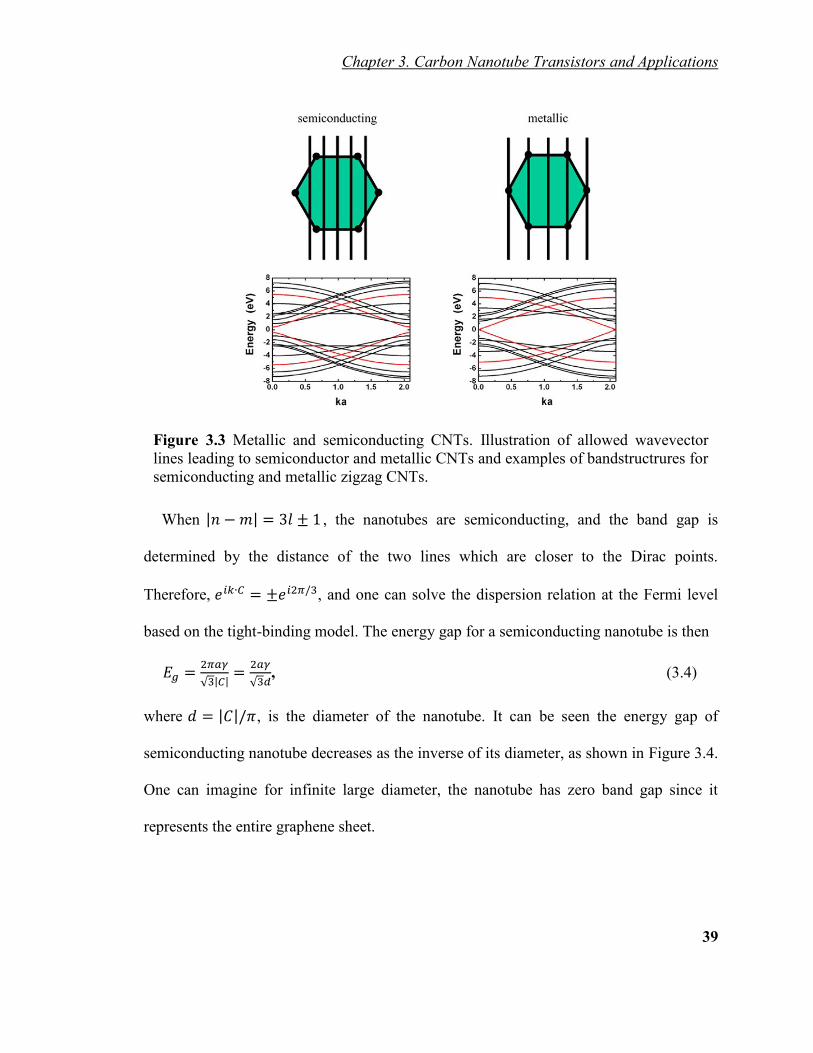
Chapter 3. Carbon Nanotube Transistors and Applications
39
Figure 3.3 Metallic and semiconducting CNTs. Illustration of allowed wavevector
lines leading to semiconductor and metallic CNTs and examples of bandstructrures for
semiconducting and metallic zigzag CNTs.
When , the nanotubes are semiconducting, and the band gap is
determined by the distance of the two lines which are closer to the Dirac points.
Therefore, , and one can solve the dispersion relation at the Fermi level
based on the tight-binding model. The energy gap for a semiconducting nanotube is then
√
√ , (3.4)
where , is the diameter of the nanotube. It can be seen the energy gap of
semiconducting nanotube decreases as the inverse of its diameter, as shown in Figure 3.4.
One can imagine for infinite large diameter, the nanotube has zero band gap since it
represents the entire graphene sheet.

Chapter 3. Carbon Nanotube Transistors and Applications
40
Figure 3.4 Band gap versus radius for zigzag CNTs.
3.2.3 Deposition of Carbon Nanotubes
Overall speaking, the ideal fabrication methods should provide good control in terms
of the key parameters of the thin film. Particularly for CNTs thin films, these parameters
may include film density (or coverage), ratio of m-CNTs and s-CNTs, alignment,
distributions of lengths and diameters of nanotubes, etc. It is also important to be
compatible with large-area, low-cost processing, or maybe on flexible substrates for some
applications. This section reviews some of the approaches which have demonstrated
successes in certain directions.
In order to deposit the CNTs at desired locations on substrate, many techniques have
been developed. Usually, it can be divided into categories as “grow-in-place” and
“solution-based”. The “grow-in-place” technique usually involves the synthesis of
nanotubes and deposition on substrate simultaneously. The most commonly used and
intensively studied synthesis methods of CNTs are chemical vapor deposition (CVD) and
Chapter 3. Carbon Nanotube Transistors and Applications
41
laser ablation. Typically, CVD growth of CNTs gives good control of film density or
coverage, as well as the film morphology and nanotube alignment. Growth parameters
can be adjusted to tune properties of the CNTs. For example, species of feed gas,
concentration of catalytic nano-particles influence the film density.119-122
There are
studies showed that the size and composition of catalyst may affect the diameters and
chiralities of the CNTs.123,124
In addition, the average tube length depends on the growth
temperature, gas pressure, and growth time.125,126
Some examples are shown in Figure 3.5
(a) – (c). Besides the control over the network parameters, some methods also
demonstrate the ability of achieving alignment and patterning of the CNTs. Figure 3.5 (d)
– (h) showed some examples of aligned CNT networks. The techniques which have been
demonstrated include CVD growth with electrical field,127,128
CVD growth with a laminar
feed gas flow,129-131
growth on substrates with regular atomic steps,132,133
or patterned
catalyst particles.134
Combining multiple steps of alignment control, the CNT can be even
grown in complex morphology (example in Figure 3.5 (i)).135-138
Despite the capability of
fabricating high quality CNT film, CVD growth is not very compatible to low
temperature, large area fabrication.
The “solution-based” methods, on the other hand, are more suitable to low-
temperature, large-area, and cost-effective fabrications of electronics, and thus more
attractive to many applications. The methods generally involve the formation of a stable
solution suspension of CNTs, and a reproducible way to deposit the CNTs onto substrate
from the solution. Due to the strong tube-to-tube interactions of CNTs, to achieve a stable
suspension usually requires using surfactant wrapping around the nanotubes. This step

Chapter 3. Carbon Nanotube Transistors and Applications
42
often requires high-power ultrasonication which could reduce the average lengths of
CNTs and affect the electrical properties. Furthermore, the presence of the organic
surfactant may influence the electronic properties of CNTs due to the complex surface
chemistry.
Figure 3.5 SEM/AFM images of CNT films grown by various methods. (a) and (b),
CNT films grown by CVD. (c) A CNT film deposited from a suspension in methanol.
(d) An aligned array of CNTs grown by CVD with an applied electric field between
microelectrodes (bright). (e) Crossbar array of CNTs formed by a two-step flow-
alignment growth process. (f) CNT array grown on a miscut sapphire substrate. (g)
and (h) Patterned CNT films grown by CVD. (i) Self-organized nanotube serpentines
formed due to the combined alignment effects from the quartz substrate and gas
flow.29
As to how to remove the solvent and fabricate the CNTs onto the desired substrates,
there are many different techniques. Early demonstrations by Snow et al. showed random

Chapter 3. Carbon Nanotube Transistors and Applications
43
CNT networks can be achieved by as-grown CNTs solutions, with the mobility about 10
– 100 cm2/Vs, and ON/OFF ratio of 10 – 100.
139-141 Other techniques which can
reproducibly achieve random networks include drop-casting,142-144
spin-coating,145,146
dip-coating,147
quasi-Langmuir–Blodgett148
and Langmuir–Blodgett deposition.149
These
solution-based methods not only share the advantages such as compatibility to large area
and room temperature deposition, but also have limitations such as the sensitivity to the
substrate surface energy or surface chemistry, alignment, presence of the CNTs bundles,
variations of the network morphology and densities, and so on. A technique with
controlled flocculation (cF) process demonstrated the ability of controlling the location of
CNT deposition, as well as the film density and alignment.150,151
Other efforts trying to
address the alignment of the network include gas-flow cell method,152
and coating the
substrate with functional molecules,144,147
deposition assisted by electrical or magnetic
field,153-158
and other methods such as deposition based on the liquid-crystalline behavior
of CNTs.159
Transfer printing is another class of methods which can be combined with some of
the above solution-based fabrication methods.150,151,160
Vacuum filtration method was
demonstrated by Grüner and colleagues.161
The diluted CNT solution is vacuum-filtered
through a porous membrane, and the nanotubes were trapped on the surface of
membrane, forming a thin film. The advantages of this method are the high throughput
(in a few seconds), precise control over the film density by controlling the filtered
solution volume, and homogenous film morphology due to the fast evaporation of solvent
and minimum tube flocculation. However, it may require additional transfer steps in

Chapter 3. Carbon Nanotube Transistors and Applications
44
order to accommodate different substrates.162
This method is useful for the applications
such as transparent conductance films due to the ability of achieving high density CNT
networks under fast speed.163
It has been successfully demonstrated that spin-coating,
drop-casting, dip-coating, ink-jet printing, and aerosol jet printing based on CNTs
solutions can fabricate the CNTs films on various type of substrates (examples are shown
in Figure 3.6).
Figure 3.6 Deposition methods of CNTs. (a) drop-casting of CNT thin film.140
(b) and
(c), the schematic of Langmuir–Blodgett deposition and SEM images of CNT film.151
(d) and (e), transfer printing of CNT stripes. (f) jet printing of CNT solution.164
There are several advantages of the solution-based deposition. For example, the post-
growth purification techniques have shown some success in controlling the CNT
diameters and chirality, which will directly benefit the thin film quality deposited from
purified solutions. In addition, several methods, especially printing techniques, can offer
very well control in patterning of the thin film, which is critical to electronic applications.
(a) (b) (c)
(d) (e) (f)

Chapter 3. Carbon Nanotube Transistors and Applications
45
However, the remaining challenge is the alignment of the nanotubes. Perfectly aligned
nanotubes network may be desired in low-resistance transparent electrodes applications,
but its effect on electronics based on semiconducting CNTs thin films is not yet clear.
3.2.4 Purification of CNTs
As mentioned above, the as-grown CNTs contain m-CNTs and s-CNTs. The m-CNTs
are useful to transparent electrodes and sensor applications, and the s-CNTs are good
candidates for semiconductor electronics. Therefore, in most of the applications, it is
critical to separate these two kinds of the CNTs to achieve the best device performance.
The differences in electrical, chemical and optical properties make it possible to separate
the two kinds of CNTs. Some level of control during growth has been achieved,165,166
however, the post-synthesis purification methods seem to be more promising.
Electrical breakdown is a method usually used on CNTs TFTs based on a mixture of
m-CNTs and s-CNTs. The CNTs are in “OFF” state under gate bias, and a bias between
the source and drain electrodes will induce current through the metallic nanotube paths,
thus selectively burned these paths. This technique can increase the ON/OFF ratio up to
105, without reducing the ON current substantially. The challenge of this method is to
implement it on large scale wafer or complex circuit design.
Another type of purification methods which has been extensively studied is flow-based
sorting, including electrophoresis, chromatography and ultracentrifugation based
methods.167-172
The CNTs are suspended in solutions, wrapping with surfactant, charged
polymers or DNAs, as shown in Figure 3.7 (a) and (d). The m-CNTs and s-CNTs will

Chapter 3. Carbon Nanotube Transistors and Applications
46
have different packing density of the CNT-polymer complexes, thus the separation by
ion-exchange chromatography or ultracentrifugation is possible. The > 99%
semiconducting or metallic nanotube enriched solution has been achieved in many
research labs,173,174
also commercial available.175
With ultracentrifugation, the buoyant
density is influenced not only by the type of CNTs, but also the chirality, diameter and
length, depending on the nature of the surfactant and functionalization chemistries, as
illustrated in Figure 3.7 (b) and (c).173,176
Zheng and colleagues demonstrated that 20
DNA molecules each can bind with specific CNT (n, m) with specific affinity.177
CNTs
can also be sorted by length with DNAs178
and amino acids179,180
. With continuing
research and effort, it can be anticipated that the purification of CNTs can eventually
provide monodisperse CNT solutions with selective electronic or other properties. This
will significantly benefit the fundamental research of CNTs properties. The major
challenges then remain are the cost, yield and reproducibility of the CNTs purification,
especially for industry applications.
Another difference between the m-CNTs and s-CNTs is the chemical reactivity, which
makes another separation strategy possible, wet etching. This is because the m-CNTs and
s-CNTs have different density of states near the Fermi level, which leads to different
stability in chemical reactions.181-183
Experiments and calculations show m-CNTs are
more chemically reactive than s-CNTs. For example, with certain concentration,
diazonium can selectively react with only m-CNTs and render them insulating, without
affecting the s-CNTs.181,184
This method can also be used after deposition, and the TFT
achieved 105 ON/OFF ratio.
185

Chapter 3. Carbon Nanotube Transistors and Applications
47
Figure 3.7 Suspension and purifications of CNTs. (a) schematic of surfactant
wrapping the CNTs and sorting based on density (). (b) and (c) optical image and
absorption spectra of CNTs/Sodium Cholate (SC) suspension after density gradient
ultracentrifugation (DGU).173
(d) schematic of DNA-wrapped CNT network.178
3.2.5 CNT Network
The previous discussion of band structures and electronic properties are based on
single nanotube. When the CNTs form a network, the electronic properties will become
difficult to explore because of various parameters. For example, in a network contains
both semiconducting and metallic nanotubes, which is generally true for all cases, there
will be a mixture of chirality and electrical characteristics depending on the percentage of
the purity. The CNTs network contains metallic and semiconducting nanotubes. The
(a) (b) (c)
(d)

Chapter 3. Carbon Nanotube Transistors and Applications
48
metallic nanotubes can be modeled as always “on”, with a constant resistance. The
semiconducting nanotubes can be modeled as either “on” or “off” depending on the gate
bias. Early work simulates the conductivity of CNTs network based on percolation
theory, assuming the sample is infinite and the tube-tube conductance is perfect.186
Alam
and colleagues took into account the sample size and the finite tube-tube conductance
(0.1 e2/h)
186,187 In addition, the distribution of nanotube lengths and diameters, nanotube-
nanotube junctions, network density and the level of alignment all affect the network
characteristics. In terms of the device performances, there are additional parameters to
consider, such as the ratio between channel length and nanotube lengths, the nanotube-
electrode contact resistances, quantum capacitance (especially in FETs), etc. Given so
many variables, the current work in electronics based on CNT networks are mostly based
on experimental and phenomenological studies.
3.3 Electronic Devices Based on CNTs
Many interesting and attractive applications based on CNTs have been demonstrated
or studied in the past decades. The unique electronic, mechanical, and chemical
properties of CNTs, such as high mobility, high tensile strength and elastic modulus,
large surface area, etc., continuously drive increasing attentions. This section reviews
some of the applications based on CNTs electronic properties.
As mentioned above, the electron mobility in CNTs is much higher than conventional
semiconductor, such as silicon, which makes CNTs an attractive semiconductor material.
Furthermore, the CNTs have been demonstrated with good compatibility of flexible

Chapter 3. Carbon Nanotube Transistors and Applications
49
electronics, in which area most materials suffer the low mobilities. Figure 3.8 illustrates
how the CNT mobility compared to organic semiconductors. Single CNT is an ideal
candidate for semiconductor electronics, with high ON/OFF ratio (106) and mobility
(10,000 cm2/Vs). CNT networks possess lower mobilities compared to single nanotubes,
yet much higher than organic semiconductors and amorphous silicon and compatibility to
flexible applications. The ON/OFF ratio of CNT network depends on level of
purification, fabrication methods, device parameters, etc.
Figure 3.8 Mobility and ON/OFF ratio trend and comparisons for nano-transistors.188
3.3.1 Thin Film Transistors Based on CNTs
The first field-effect transistors (FETs) based on CNTs were reported by Dekker and
Avouris at 1998.189,190
Typically, CNTs are grown on top of dielectrics (such as SiO2),

Chapter 3. Carbon Nanotube Transistors and Applications
50
making contact to metal source/drain electrodes (such as Au, Pt). The CNTs can be tuned
from the insulating state to conductive state by the gate bias. Charge carriers can then be
injected into the nanotube through source electrode and conduct electric current. As
shown in Figure 3.9, the negative gate bias may flatten the valence band of the nanotube
and switch the nanotube into conductive state (in this case, for holes), and the positive
gate bias bends the band more and deplete the holes which switch the nanotube to the
insulating state.
Figure 3.9 FETs based on CNTs. (a) AFM, (b) schematic of the thin film transistor
based on CNTs. (c) band diagram of the gating effect of the transistors. (d) effect of
drain bias on suppressing the contact barrier.189
Although the characteristics of CNT FETs can be explained and modeled by the band
theory in conventional MOSFETs, there are a number of differences between the CNT
FETs and conventional MOSFETs. First of all, the CNT FETs operate mostly under
accumulation mode not depletion mode. The charge carriers are injected from the source

Chapter 3. Carbon Nanotube Transistors and Applications
51
electrode. Since the energy band gap of semi-CNTs are small, the CNT FETs often
behave as ambipolar FETs, as shown in Figure 3.10, as long as the contact barrier at both
source and drain electrodes are low. For some applications, ambipolar transistors have
their own advantages, while some other applications may prefer unipolar transportation.
The type of transportation is affected by the chemical doping of the CNTs,191-193
the
Fermi level of contact metals,194-196
the dielectric materials,82,197,198
etc.
Figure 3.10 Ambipolar transportation of FET based on CNTs. Left inset shows the p-
type transportation (hole) under negative gate bias. Right inset shows the n-type
transportation (electron) under positive gate bias.108
In CNT FETs, the quantum capacitance CQ, which is the capacitance related to the
density of states, is small (~10-10
F/m).199
In conventional MOSFETs, the gate
capacitance, CG, is smaller than CQ. Therefore, the gate capacitance is the dominant
factor controlling the band diagram of semiconductor layer. However, in some CNT

Chapter 3. Carbon Nanotube Transistors and Applications
52
transistors (scaled down or using high dielectric constant materials), CQ ~ CG, or even CQ
< CG, hence the quantum capacitance may become dominant.
3.3.2 Scaling of CNT FETs
Due to the quasi 1-D structure of CNTs, the scaling effect of the CNT transistors is
different from conventional MOSFET. In conventional devices, the key performance
parameters, e.g., mobility, is usually independent of the dimensions of the semiconductor
layer. However, in CNT FETs, the average length of nanotubes, ratio of nanotube length
to channel length, density, purity, and alignment may all play a role in mobility and
ON/OFF ratio. Some study in CVD grown, aligned CNT network, shows that the
mobility increases with the channel length, which might include the contact resistance
effect.200
There are also other reports about the scaling effects of channel length on
mobility, suggesting the dependence may be weak.201-204
Currently, the channel length
dependence of mobility is not fully understood theoretically.
The coverage density of CNT networks has a strong impact on the mobility and
ON/OFF ratio, especially on the as-grown CNT networks grown by CVD. For unpurified
CNTs, due to the presence of metallic nanotubes, when the m-CNTs are below the
percolation threshold while the s-CNTs are above the percolation threshold, the network
may achieve the optimum ON/OFF ratio.28,205
Sangwan and colleagues found, using
Monte Carlo simulation, the ON/OFF ratio had a transition around 0.2 ~ 0.3
CNTs/m2.205
For purified CNTs, the ratio of m-CNTs is much lower (up to 2 orders)
than unpurified CNTs, which will be below the percolation threshold in most of the

Chapter 3. Carbon Nanotube Transistors and Applications
53
networks. The dependence of the ON/OFF ratio on purified network density was studied
by a couple of groups.201,206
The density dependence of purified network is less
significant than unpurified one,188
which could be due to the purification, the difference
of nanotube length and chemistry.
In general, the higher density of the network, the higher the mobility and lower the
ON/OFF ratio will be. Burke et al. summarized the mobility and ON/OFF ratio in the
CNT networks in their review paper based on all recent studies, as shown in Figure
3.11.188
The network based on unpurified CNTs (red and green) lines showed a clear
transition due to the high ratio of metallic nanotubes, while the purified network showed
similar but smoother trend. This plot illustrated the relationship between the ON/OFF
ratio and mobility in CNT networks. Despite the CNT properties (length, chirality, and
diameter), fabrication methods, device architecture, etc., are different from one research
group to another, the trend is clear. Additionally, the purified CNT networks showed
improved mobility and ON/OFF ratio. It worth to note that, currently the studies seemed
to be phenomenologically, however, a roadmap for practical applications may be
established with further fundamental studies.
One of the attractive advantages of CNT based electronics is their potential on
flexible, transparent electronic applications.207
Transparent, conductive CNTs film can be
fabricated by vacuum transfer method on wafer scale.163
Rogers group also demonstrate
bendable TFT arrays patterned by transfer printing (a dry printing technique), with
effective mobility up to 30 cm2/Vs.
122 In addition to these, the transparent conductive
CNT film also provides potential application in optical electronics, such as organic light

Chapter 3. Carbon Nanotube Transistors and Applications
54
emitting diode (OLED) and organic photo-voltaic devices (OPV), since CNT is a good
contact material to organic semiconductors.208
In Chapter 7, a printed transparent CNT
thin film functions as a good contact electrode to the electrochromic devices.
Figure 3.11 Mobility and ON/OFF ratio of CNT network. Solid blue line is for
purified inks, red and green lines are for unpurified inks and as-grown networks. The
data points of each method are shown in the insets.
3.3.3 CNT Circuits and Other Applications
Thanks to the high mobility, CNTs have been considered as a good candidate of next
generation semiconductor electronics. In the area of high frequency applications, Avouris
and colleagues demonstrated a 5-stage CMOS ring oscillator based on a single CNT in
2006, which achieved 52 MHz frequency (Figure 3.12).194
The ring oscillator used an
18m long s-CNT as the semiconductor, Al2O3 as dielectric, and Pd as the gate of n-FET,

Chapter 3. Carbon Nanotube Transistors and Applications
55
Al as the gate of p-FET. Each stage includes one n-FET and one p-FET to form a CMOS
inverter.
Figure 3.12 A 5-stage ring oscillator fabricated on a single CNT. (a) SEM image of
the 5 stages of CMOS inverters. (b) Voltage-dependent frequency spectra.194
Dai’s group also demonstrate thin film transistors (TFTs) and digital circuits based on
individual CNTs. 209
CNTs were CVD grown on substrate which was pre-patterned with
bottom W gate electrode, molybdenum source and drain electrodes, and catalyst. The
grown CNT bridged through the source and drain electrodes and formed semiconducting
transistors (~70% of the transistor array). The TFTs are p-type as fabricated, but can be
turned into n-type with desorbing of oxygen in vacuum. By wire bonding several
transistors together, the team achieved NOR, OR, NAND and AND logic gates. The
three-stage ring oscillator showed 220 Hz frequency and 0.75ms stage delay time. There
are a few disadvantages of circuits based on individual CNT. First of all, the fabrication
process requires many challenging steps which are unlikely to be compatible with low-
(a) (b)

Chapter 3. Carbon Nanotube Transistors and Applications
56
cost, flexible electronics. In addition, the variation from device to device is too large to
applications. This is mainly due to the distribution of as-grown CNTs, such as diameters,
length, chirality, types, etc. Therefore, this type of devices may be a great platform to
study the CNTs properties, but not necessarily a promising direction of CNT applications.
This brings to the attention the electronics devices based on arrays of CNTs.
RF devices: Application in radio frequency (RF) devices is one of the advantages of
CNTs due to their high intrinsic mobility (~104 cm
2/Vs), small capacitance (~100
aF/mm), and nanometer-thick channel. The aligned CNT arrays grown on quartz
substrate showed most promising performance. The cut-off frequency for TFTs can be up
to 10 GHz, with low density CNT film (5 CNT/m).210
RF power amplifiers which can
be integrated with a functional analog electronic system have also been explored.211
The
CNT TFTs achieved >1 power gain in very-high-frequency range. Another component of
analog RF system, oscillators, achieved 500 MHz with devices based on CNTs.212
Gas sensors: CNT consists only with surface atoms, which makes it extremely
sensitive to surface environment, such as the chemistry change. These changes can be
reflected by the electronic property of CNTs, and be sensed by resistors, transistors or
capacitors based on CNTs. CNT array is usually used in sensor devices in order to
enhance the signal to noise ratio and achieve the reproducible performance. A simple
chem-resistor can be used to detect the presence of certain toxic gas in ppb level.213
With
gas molecules absorbed to the surface defect points, the apparent resistance of CNT will
change which is due to the charge transfer between the absorbed molecules and the

Chapter 3. Carbon Nanotube Transistors and Applications
57
valence band of CNTs.214
The stronger electron donating or withdrawing capability the
molecules have, the larger change of CNT resistance will be. However, there are two
major drawbacks of CNT gas sensors. First, the specificity is low, since many molecules
can be absorbed and result in similar effect. Certain type of functionalization can be
helpful.215,216
Second, the recovery process is usually slow due to the slow desorbing
process. Using TFT type of device can speed up this process by applying gate voltage.213
Biosensors: CNTs have been demonstrated with good potentials in biosensor area. As
previously mentioned, charged large molecules, such as DNAs and proteins, can bind to
the surface of SWTN, and alter the conductance of CNT thin films. Similar as the gas
sensors, CNT can be fabricated as resistors or transistors to provide a label-free detection
of bio molecules.217,218
The detection limit can achieve picomolar- or even femtomolar-
level.219,220
By pre-coating the device with some antigens, selective detection is also
possible.219

Chapter 4. Printed and Flexible Circuits and Applications
58
Printed and Flexible Circuits and Applications Chapter 4
4.1 Introduction
Any material can be flexible when its thickness comes down to a certain scale. The
concept of flexible electronics started decades ago, when the solar cell devices based on
single crystal silicon scaled down to ~ 100 m and exhibited the flexibility to be
assembled on plastic substrates.221
Later on, the hydrogenated amorphous silicon (a-
Si:H), which can be deposited at low temperatures, enabled the direct fabrication of solar
cells on flexible substrates.222
Since 1980s, the roll-to-roll fabrication of a-Si:H on
flexible metal foil and plastic substrate has been introduced and widely used in
industry.223
Flexible thin film transistors (TFTs) and circuits also date back to 1960s,224
and developed wide applications including the backplanes for active-matrix liquid-crystal
display (AMLCD), flexible LCD, and flexible organic light-emitting diode (OLED)
display.
This chapter reviews the fabrication techniques of flexible transistors, circuits and
their applications, with a specific focus on the printed electronics. In addition, the recent
progresses on flexible electronics are also reviewed, such as the circuit performance,
demonstration of complementary circuits, and applications in large area display, RFID
tags, etc.

Chapter 4. Printed and Flexible Circuits and Applications
59
4.2 Fabrication of Flexible Circuits
There are different levels of flexibility in flexible electronics, including bendable,
conformally shaped, elastic/stretchable, roll-to-roll manufacturable, etc. Over the decades
of researches, flexible electronics have been demonstrated based on inorganic materials,
such as a-Si, compound semiconductors, and nano-materials, as well as organic materials,
such as small molecules and polymers. These materials can be directly grown on the
flexible substrates, assembled after, or fabricated directly by solution-based processes.
This section briefly reviews the experimental works of the flexible electronics based on
various fabrication methods.
4.2.1 Deposition Methods from Gas-phase
The direct growth fabrication methods are similar as in the conventional
semiconductor industry, such as the chemical vapor deposition (CVD) approaches. The
challenge of this type of techniques is the trade-off between the process temperatures and
the semiconductor film qualities.225
With the limits of process temperatures not exceeding
the glass transition temperature of the polymer-based substrates, the thin films usually
could not achieve large scale of crystallinity. In addition, many steps of the growth
process and following fabrication processes do not easily scale to the large areas.
Inorganic semiconductors: Amorphous silicon is a semiconducting material most
widely employed in the large area applications, by far. Typically, high-quality a-Si films
require relative high temperature (> 250 °C) during deposition, but low-temperature
processes are demonstrated.226-228
For example, TFTs fabricated on PET substrate by RF-

Chapter 4. Printed and Flexible Circuits and Applications
60
PECVD at temperatures < 100 °C showed mobilities around 0.4 cm2/Vs and ON/OFF
ratio > 105.229
The qualities of the a-Si:H films fabricated under low temperatures can be
significantly improved by post-deposition processes which transform them into poly-
crystalline silicon films, including solid-phase crystallization, excimer-laser annealing, or
sequential lateral solidification.230
These process can lead to large-grain films and good
performance, such as TFTs with mobilities >60 cm2/Vs after annealing at 650 °C.
231
In addition, compound semiconductors can also be deposited at low temperatures onto
flexible substrates, by radiofrequency magnetron sputtering and pulsed-laser deposition.
For example, ZnO films deposited on flexible polyimide substrate by pulsed-laser
deposition were demonstrated,232
although the transistors based on ZnO were mostly
studied on glass substrates.233
Hosono’s group demonstrated TFTs based on amorphous
In-Ga-Zn-O films and achieved mobilities > 6 cm2/Vs.
Organic semiconductors: Although the electrical performance is lower than
crystalline silicon, organic small molecules and polymers are attractive alternatives for
flexible electronics, due to their mechanical flexibility and compatibility to low
temperature process. The major challenge of organic semiconductors is the lower
mobility (detail discussions are in section 2.1), however, many promising results have
been demonstrated in the last decades.
Single crystal small molecules can be grown from solution, or physical vapor transport
(PVT) method. The single crystal materials can achieve relative high mobilities, e.g., the
mobility of Rubrene single crystal can achieve up to 20 cm2/Vs.
44 Fabrication of
transistors based on these materials is usually difficult to apply on integrated circuits.

Chapter 4. Printed and Flexible Circuits and Applications
61
Figure 4.1 Flexible OTFTs based on Pentacene. (a) an array of OTFTs fabricated on
polyimide substrate.234
(b) the scheme of typical flexible transistor with evaporated
Pentacene.235
Thermal evaporation of organic small molecules is a method compatible to
conventional photolithography. Kane et al. reported Pentacene OTFTs and circuits
fabricated on polyester film.236
The Pentacene was deposited by thermal evaporation at
about 60 °C, achieved mobility 0.03 – 0.45 cm2/Vs. The operation voltage range is 20 V.
With yield of 65%, they were able to fabricate digital circuits including frequency
divider, differential amplifier, and ring oscillator. Klauk et al. later compared the
performance of Pentacene OTFT and ring oscillators fabricated both on glass and
polyethylene naphthalate (PEN) film.235
Due to the higher roughness of PEN substrate,
the trap density of Pentacene might be higher and resulted in slightly lower mobility (0.3
cm2/Vs on PEN, 0.7 cm
2/Vs on glass), higher threshold voltage and subthreshold swing.
Someya et al. reported OTFTs on large area (8 × 8 cm2) polyimide substrate, where all of
a.
b.
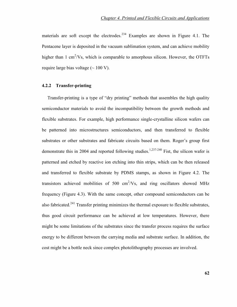
Chapter 4. Printed and Flexible Circuits and Applications
62
materials are soft except the electrodes.234
Examples are shown in Figure 4.1. The
Pentacene layer is deposited in the vacuum sublimation system, and can achieve mobility
higher than 1 cm2/Vs, which is comparable to amorphous silicon. However, the OTFTs
require large bias voltage (~ 100 V).
4.2.2 Transfer-printing
Transfer-printing is a type of “dry printing” methods that assembles the high quality
semiconductor materials to avoid the incompatibility between the growth methods and
flexible substrates. For example, high performance single-crystalline silicon wafers can
be patterned into microstructures semiconductors, and then transferred to flexible
substrates or other substrates and fabricate circuits based on them. Roger’s group first
demonstrate this in 2004 and reported following studies.1,237-240
Fist, the silicon wafer is
patterned and etched by reactive ion etching into thin strips, which can be then released
and transferred to flexible substrate by PDMS stamps, as shown in Figure 4.2. The
transistors achieved mobilities of 500 cm2/Vs, and ring oscillators showed MHz
frequency (Figure 4.3). With the same concept, other compound semiconductors can be
also fabricated.241
Transfer printing minimizes the thermal exposure to flexible substrates,
thus good circuit performance can be achieved at low temperatures. However, there
might be some limitations of the substrates since the transfer process requires the surface
energy to be different between the carrying media and substrate surface. In addition, the
cost might be a bottle neck since complex photolithography processes are involved.

Chapter 4. Printed and Flexible Circuits and Applications
63
Figure 4.2 Schematic process flow of single-crystal silicon ribbon fabrication.
(a) plasma etch. (b) passivation of the sidewalls. (c) undercut of the Si ribbons. (d)
Cross-sectional SEM image of partially undercut ribbons. (e) Released, flexible
ribbons.242
In addition, nanowires or other nanostructures of semiconductors can also be
synthesized and then transfer print onto flexible substrates. The work on circuits by
transfer printing of carbon nanotubes is reviewed in section 3.2.2.
Figure 4.3 Ring oscillators based on ribbon of silicons. (a) image of an array of ring
oscillators patterned on flexible substrate. (b) output performance of ring oscillators. 240

Chapter 4. Printed and Flexible Circuits and Applications
64
4.2.3 Deposition Methods from Liquid-phase
Previous sections review the fabrication methods which mostly based on gas phase,
such as evaporation, sputtering, CVD, etc. Another attractive route to achieve flexible
electronics is the solution-based processes, such as spin-coating, drop-casting, and
additive printing. The printing process will be discussed in details in section 4.3 since it is
a major focus of this thesis.
The solution-based process is cost-effective, low temperature, and easy to scale up to
large areas. Almost any materials that can be prepared in solutions or suspensions, such
as polymers, small molecules, and nanostructures of materials, are solution processable.
The first all-polymer OTFT integrated on plastic substrate is reported by Philips Research
Labs in 1998.243
The transistors were fabricated by spin coating of electrically active
precursors on polyimide foil and patterned by exposure of UV light through masks. The
p-type transistors with 2 m channel length and 2 mm channel width achieved mobility
of 2×10⁻⁴
cm2/Vs. The authors were also able to demonstrate a 15-bit code generator
integrated of 326 transistors.
Small molecules (or precursors) and oligomers can be dissolved and then deposited on
substrates by drop-casting or spin-coating.244
For example, many interesting Pentacene
derivatives and precursors have been studied and demonstrated solution-processable, with
hole mobilities as high as 1 cm2/Vs.
245,246
Solution processed films are often considered to have relative lower quality due to the
variation of thickness (especially dielectrics), roughness, morphology, etc. Many

Chapter 4. Printed and Flexible Circuits and Applications
65
researches try to address these challenges and improve the device performance. For
instance, it appeared that the grain boundary orientation in drop-casted small molecules
thin film has modulation of carrier transport,247
hence controlling the crystallinity of the
semiconductor film can further improve the device performance.248
The interactions
between semiconductor and dielectric layers are also intensively studied.249
It is often challenging to pattern the organic films in the solution-based depositions. In
addition to the photochemical patterning described above,243
some studies employ hybrid
structures, e.g., organic semiconductors together with inorganic conductive and dielectric
layers which can be patterned by standard photolithography, and define the organic layers
by etch masks and plasma etching.250,251
Soft lithography using prepatterned elastomeric
materials, such as PDMS, to transfer micrometer or nanometer scale structures, has been
demonstrated in fabricating OTFTs.252-254
4.3 Printing Techniques for Electronics
Printing is fast-speed, low-cost, and additive technique for flexible electronics. The
conventional paper printing is widely used every day, with printing speed up to 100 km/h.
The methods of printing electronic materials share the same concepts of printing, but are
more sophistic than that. In conventional newspaper printing, the “printing quality”
usually refers to resolution and registration of pigment dots. There are a lot more to
consider when printing functional electronics. Electronic devices consist of multiple
layers, and each has its own specifications of “quality”. For example, conductive layer
need to be continuous and low-resistance; dielectric layers require uniform thickness

Chapter 4. Printed and Flexible Circuits and Applications
66
without pinholes; and semiconductor layers may require more control over film
thickness, morphology and alignment for optimized performance.
Traditional printing techniques include Gravure, flexography, offset, and screen
printing, which all can be used in Roll-to-Roll (R2R) process. Digital printing techniques,
such as ink-jet printing and aerosol jet printing are also well developed in flexible
circuitry fabrications. The key parameters of common printing techniques are compared
in Table 4.1. Details of these printing techniques are described below.
Table 4.1 Comparison of common printing techniques. 255
Flexographic printing. In flex printing, a flexible plate carried the printing patterns is
attached to a cylinder. The plate is usually patterned by photolithography in the way that
the image area is raised above the non-image areas. The plate surface is inked when in
contact with an anilox cylinder surface which is previously inked. And the pattern is
finally transferred to substrate by the plate cylinder (Figure 4.4 a). Flex printing is used in
printing conductive materials, OTFTs, and organic circuits.17,256-258

Chapter 4. Printed and Flexible Circuits and Applications
67
Gravure printing. Gravure printing, also known as rotogravure printing, is one of the
most widely used printing techniques for flexible electronics, include organic solar cells,
organic light-emitting diodes, and OTFTs.257-261
As shown in Figure 4.4 b, the gravure
cylinder picks up the inks from fountain when it rolls. A doctor blade removes the excess
ink from the cylinder surface before it is in contact with the substrate, which is
sandwiched in between the impression roller and the gravure cylinder. The patterns,
which are engraved on the gravure cylinder by lithography or chemical etching, are
printed on the substrate.
Figure 4.4 Common printing process. (a) Flexographic printing,262
(b) Gravure
printing, 259
(c) Offset printing,263
Offset printing. Offset printing is a common printing technique but there are some
limitations for printed electronics. This technique employs several cylinders to transfer
the ink so the ink can be evenly distributed. The resolution and printing quality of this
a
b
c

Chapter 4. Printed and Flexible Circuits and Applications
68
technique can be good since the rubber offset cylinder can make a conformal contact to
the substrate, as shown in Figure 4.4 (c). This technique is a fast-speed and low-cost
printing method, but the demonstration in printed electronics is rare.264,265
Screen printing. Screen printing is often used as a flat printing technique, but is
adaptable to R2R process. Typically, a high viscosity ink is dragged across the surface of
a mesh screen and squeezed through the patterned pores onto the substrate. The printing
resolution and quality depends on the ink viscosity and pores density. Screen printing can
print relatively thick layers, which is an advantage for conductive layers.260,266
Figure 4.5 Ink-jet printing mechanism. (a) Typical printhead of ink-jet printer. (b)
Pictures of a droplet ejecting from the printhead, after 40 s and 360 s after the
voltage pulse, respectively.267
Ink-jet printing. Ink-jet printing has been intensively studied in the area of printed
electronics recently, and its application in printed solar cells, antennas, and OTFTs are
demonstrated.267-270
It typically employs the low viscosity inks and piezoelectric drop-on-
demand printhead, as shown in Figure 4.5. When a voltage is applied to the piezoelectric
a b

Chapter 4. Printed and Flexible Circuits and Applications
69
actuator, a sudden volume change in the capillary pushes a droplet of ink out of the
nozzle. The surface energy of the droplet, the friction of ambient air, and the voltage
applied all affect the speed of the droplets. The major advantage of the ink-jet printing is
the low-cost, and digital programmable printing patterns. On the other hand, the ink
viscosity, printing speed, and the evaporation kinetics of printed inks often result in
complicate interactions, and affect the printing resolution and quality.271,272
Figure 4.6 Scheme of aerosol jet printing. 1. liquid ink is atomized and a dense
aerosol is created. 2. The aerosol is transported to print head by a carrier gas. 3.
Aerosol is focused by a sheath gas and pushed out with a high velocity.273
Aerosol jet printing. Aerosol jet printing is also an additive digital printing technique
which has been demonstrated in functional printing recently. Instead of the liquid ink
itself, it prints a dense aerosol which is created from liquid inks. The aerosol is
transported to the print head by a carrier gas and focused by a sheath gas at the head. The
droplets, which dimensions are between 1~5 m, are then pushed out with a high velocity

Chapter 4. Printed and Flexible Circuits and Applications
70
and deposited on the substrate, as shown in Figure 4.6. The printing mechanism of
aerosol jet printing is different than ink jet, where the aerosol is carried by a gas flow.
This brings several advantages: 1), printing speed can very high (200 mm/s). 2), the
standing distance between the head and substrate can be several millimeters, since the
distortion from the ambient air is negligible. 3), the focus sheath gas provides the
flexibility of printing line width. In addition, aerosol jet printing can accommodate a wide
range of ink viscosities.
4.4 Performance and Applications of Flexible and Printed Circuits
4.4.1 Operation Speed of Flexible and Printed Circuits
Clock frequency is one of the key performance parameters in electronics, which
indicates how fast the circuits can operate. Ring oscillator, a series of inverters, is used to
generate a spontaneous oscillating signal (Figure 4.7). The time it takes for a signal to
pass through one inverter stage is usually referred as stage delay time, which is given as
tD=1/2Nf, where N is the number of stages, and f is the output frequency. This time
constant is often considered as a benchmark of circuit speed, which reflects limitations of
both intrinsic materials properties and device architectures.
Figure 4.8. summarizes the stage delay time of ring oscillators acquired from non-
printed (evaporated, spin-coated, etc.) organic circuits, printed organic circuits, and
printed circuits based on non-organic materials, displayed as a function of supply voltage.
Although the data summarized here are not all demonstrated with flexible substrates,
these studies are potentially adaptable for flexible applications.
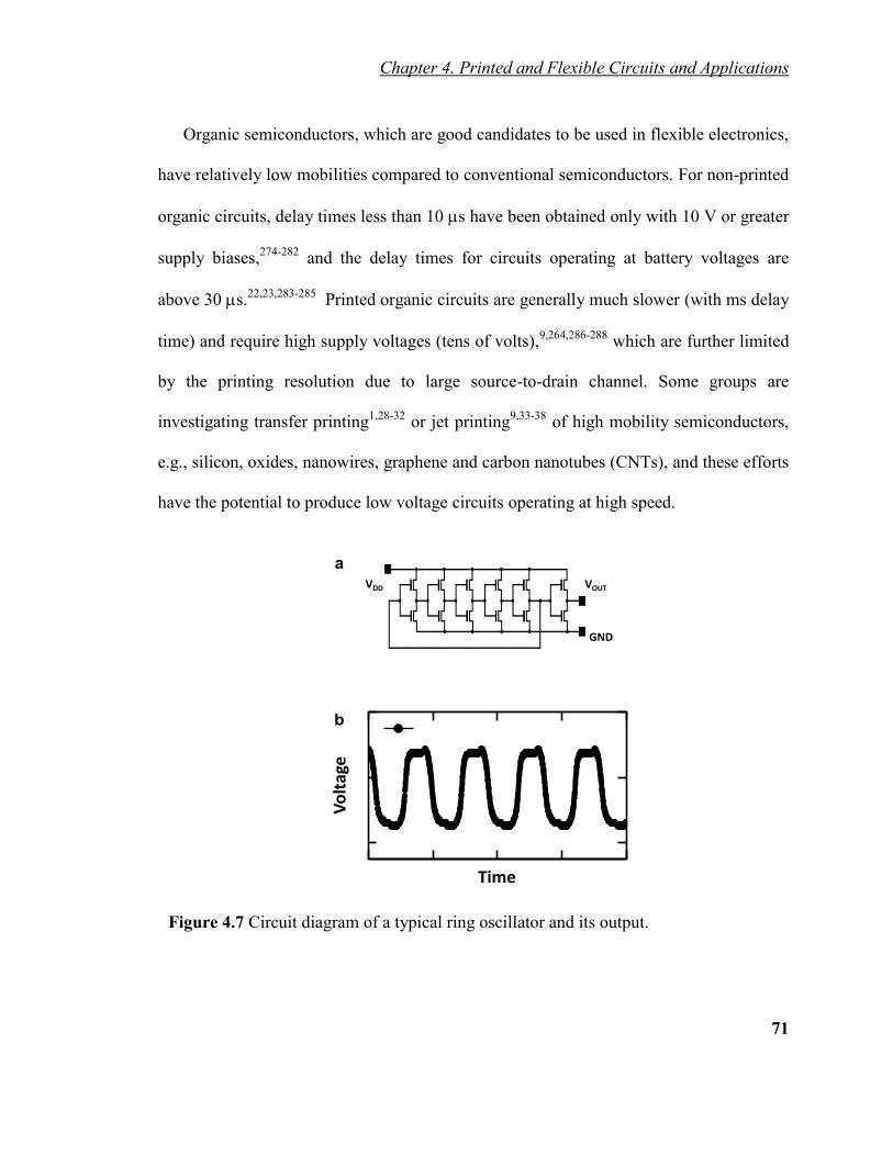
Chapter 4. Printed and Flexible Circuits and Applications
71
Organic semiconductors, which are good candidates to be used in flexible electronics,
have relatively low mobilities compared to conventional semiconductors. For non-printed
organic circuits, delay times less than 10 s have been obtained only with 10 V or greater
supply biases,274-282
and the delay times for circuits operating at battery voltages are
above 30 s.22,23,283-285
Printed organic circuits are generally much slower (with ms delay
time) and require high supply voltages (tens of volts),9,264,286-288
which are further limited
by the printing resolution due to large source-to-drain channel. Some groups are
investigating transfer printing1,28-32
or jet printing9,33-38
of high mobility semiconductors,
e.g., silicon, oxides, nanowires, graphene and carbon nanotubes (CNTs), and these efforts
have the potential to produce low voltage circuits operating at high speed.
Figure 4.7 Circuit diagram of a typical ring oscillator and its output.
Time
b
Vo
ltag
e
VDD VOUT
GND
a

Chapter 4. Printed and Flexible Circuits and Applications
72
The large voltages are not practical for many potential applications of flexible
electronics where power will be supplied by thin film batteries or radio-frequency fields.
Very recently, unipolar, p-type electrolyte-gated ring oscillator circuits have been
demonstrated that indeed operate at very low supply voltages (brown symbols), but the
shortest delay times were 200 s for devices with rather short (2.5 m) channel
lengths.25,289
Thus, a major challenge for printed electronics is to develop inks and
printing methodologies that allow shorter delay times at low supply voltages, i.e., to
move further into the pink shaded region of Figure 4.8.
Figure 4.8 Stage delay time of ring oscillators. Blue open symbols represent the non-
printed organic ring oscillators; green solid symbols represent the printed ring
oscillators; orange symbols are from printed carbon nanotube ring oscillators; brown
solid symbols are electrolyte-gated organic ring oscillators. The two star symbols are
from the work in this thesis (discussed in chapter 4 and 5, respectively).
10-6
10-4
10-2
100
1 10 100
lower voltage
De
lay p
er
sta
ge
(s)
10-1
10-3
10-5
Supply Voltage (V)
fas
ter
1 10 100
1E-6
1E-5
1E-4
1E-3
0.01
0.1
1
Dela
y t
ime o
f sin
gle
sta
ge (
s)
Supply Voltage (V)
Non-printed
organics
1 10 100
1E-6
1E-5
1E-4
1E-3
0.01
0.1
1
Dela
y t
ime o
f sin
gle
sta
ge (
s)
Supply Voltage (V)
Non-printed
organicsElectrolyte-
gated
organics
1 10 100
1E-6
1E-5
1E-4
1E-3
0.01
0.1
1
Dela
y t
ime o
f sin
gle
sta
ge (
s)
Supply Voltage (V)
1 10 100
1E-6
1E-5
1E-4
1E-3
0.01
0.1
1
Dela
y t
ime o
f sin
gle
sta
ge (
s)
Supply Voltage (V)
Non-printed
organics
Printed
organics
Electrolyte-
gated
organics
1 10 100
1E-6
1E-5
1E-4
1E-3
0.01
0.1
1
Dela
y t
ime o
f sin
gle
sta
ge (
s)
Supply Voltage (V)
Printed CNT
Printed
organics
Non-printed
organicsElectrolyte-
gated
organics

Chapter 4. Printed and Flexible Circuits and Applications
73
4.4.2 Complimentary Circuits: Low Power Operation
The majority of the printed organic transistors and circuits are unipolar, which means
only one type of charge carriers transports across the channel. In principle, both electrons
and holes should be able to transport in intrinsic organic semiconductors, however, in
most organic semiconductors, hole mobility is much higher than electron mobility. The n-
type transportation in OTFTs has typically suffered from materials degradation or
insufficient operational stability. Therefore, the majority reported printed circuits are
based on p-type channels. The unipolar circuits not only have higher circuit complexity,
but also much higher power consumption. Complementary circuits, a concept from
CMOS silicon circuits, which consists both p- and n-type channels, can truly achieve low
power circuits for portable, disposable, and light-weight applications.
Klauk et al. demonstrated a series study on low-voltage, low-power organic
complementary circuits. 23,67,275
They employed a low-leakage gate dielectric layer which
is a self-assembled monolayer (SAM), and enabled the transistor operation at 1.5 – 3 V.
And they fabricated complimentary inverters and ring oscillators with two air-stable
organic semiconductor materials for both p-type and n-type transport. Although the
devices were demonstrated on glass substrate, the process may also be applied on flexible
substrate.
Facchetti et al. demonstrated solution-processed complementary circuits on flexible
substrate, based on the air-stable, n-type small molecules developed by Polyera Corp.290
The spin-coated and drop-casted semiconductor film showed mobilities between 10-2
–
Chapter 4. Printed and Flexible Circuits and Applications
74
10-3
cm2/Vs. the complementary ring oscillator showed large output swing, with 75 Hz
frequency. They also demonstrated complementary inverters based on a n-type polymer
by gravure printing and ink-jet printing.17
Some groups also studied ink-jet printed,
complementary ring oscillators based on polymers.291
4.4.3 Other Applications: Displays, RFID, and Sensors
The research on flexible circuits has been motivated due to many promising
applications which cannot be easily realized by conventional electronics. The three major
applications of flexible circuits are flexible display, large area sensors, and RFID tags.
Display. The most compelling application for flexible circuits is the active matrix
displays, including active matrix liquid crystal displays (AMLCDs), active matrix
electrophoretic displays, active matrix electrochemical displays, active matrix organic
light-emitting diodes (AMOLEDs), etc. The active matrix display requires each display
pixel to be driven individually, therefore, it is more costly than passive display.
The first OTFT display was reported in 2001, which was a 16x16 electrophoretic
display driven by pentacene TFTs on PET substrate.292
After that, many groups
demonstrated using organic OTFTs as the backplane of flexible displays, including a 10’’
electrophoretic display on PET substrate from Plastic Logic, and a 15’’ color AMLCD on
glass from Samsung.2,3
OLEDs can also be driven with OTFTs since the voltage is
compatible. Using OTFT to drive single pixel of OLEDs was reported in 1998,293
followed by demonstrations of display matrix on glass substrates.294,295
In 2005, a 48×48
AMLED displays driven by OTFTs are demonstrated on PET substrate.4 Recently, our

Chapter 4. Printed and Flexible Circuits and Applications
75
group reported using printed electrolyte-gated transistors to drive single pixel of OLED,
which demonstrated the performance of printed OTFTs is also good for OLED display.296
Another interesting example of flexible displays is the flexible electrochromic (EC)
displays. Several groups have demonstrated active matrix control of flexible
electrochromic displays.15,104,105
The work has been reviewed in details in chapter 2.
RFID. Radio frequency identification (RFID) is a very popular application of flexible
electronics. Low-cost, disposable, and low-voltage RFID can replace the optical barcode
system which is widely used in supply chain and other areas. RFID based on silicon chips
are relatively expensive (>20 cent) for many low cost items, the desired price for printed
RFIDs is lower than 1 cent. Heremans et al. demonstrated 128-bit flexible RFID tags
based on pentacene by evaporation (Figure 4.9a).6,297
de Leeuw et al. also presented a 64-
bit tag with 1938 pentacene OTFTs on polyimide substrate.298
Figure 4.9 Flexible RFID tags. (a) Flexible RFID tag based on evaporated pentacene. 297
(b) all-printed 1-bit RFID tags.9
The first all-printed RFID tag is reported by Jung et al., combined gravure, ink-jet, and
pad printing techniques, with estimated cost of 3 cents (Figure 4.9b).9 The transistor and
circuits are based on ink-jet printed single-wall carbon nanotubes, which exhibit
a b

Chapter 4. Printed and Flexible Circuits and Applications
76
mobilities of 5 cm2/Vs and 60 Hz frequency. Although this is only a 1-bit tag, it does
demonstrate the possibilities of achieving low-cost, RFID tags by mass-printing
techniques.
Sensors. Someya et al. first demonstrated the concept of integrating the flexible
OTFTs to sensor arrays and realized the e-skin for next generation robots. The OTFTs
based on evaporated pentacene achieved mobilities around 1 cm2/Vs. They were
fabricated on flexible substrate as an active matrix and integrated with pressure and
thermal sensors, and provided 2D pressure/temperature reading.7,299
Using similar
technique, they also reported a 72×72 flexible image sensor array, by coupling the active
matrix of OTFTs with organic p-n photodiodes (Figure 4.10 left).300
Although above
circuits were still fabricated with conventional clean room facilities, they represent the
next generation of flexible electronics applications.5
Figure 4.10 Flexible sensors. Left panel: an active matrix of organic image sensors.300
Right panel: a printed humidity sensor diode integrated with RFID tags. 301
Many organic materials themselves are good candidates for gas, chemical, humidity
sensors, since their electronic properties strongly depend on the environment change.
Many research groups have demonstrated printed humidity and temperature sensors on

Chapter 4. Printed and Flexible Circuits and Applications
77
flexible substrates. Integrated with RFID tag, the sensors can transfer the readings
wirelessly (Figure 4.10 right).301,302

Chapter 5. Printed Flexible Electrolyte-gated CNT Transistors and Digital Circuits
78
Printed Flexible Electrolyte-gated CNT Chapter 5
Transistors and Digital Circuits*
5.1 Introduction
Semiconducting carbon nanotubes are known to exhibit very high intrinsic mobilities
(~ 100,000 cm2/Vs)
303 and consequently can be incorporated in high frequency (short
delay time) devices.194
Yet the difficulties associated with circuit fabrication based on
single CNTs have hindered their wide application. To overcome this, CNT thin films
deposited from solution or by dry transfer printing process have become attractive
alternatives.9,143,202,304-307
Combining printable high capacitance dielectrics with printable
high mobility semiconductors could potentially solve these problems.
This chapter demonstrates the fast, flexible digital circuits based on semiconducting
carbon nanotube (CNT) networks and high capacitance ion gel gate dielectrics, which
were patterned by jet printing of liquid inks. Electrolyte-gated transistors (EGTs) based
on CNTs with 50 m channel lengths display ambipolar transport with electron and hole
mobilities > 20 cm2/Vs; these devices form the basis of printed inverters, NAND gates,
and ring oscillators on both polyimide and SiO2 substrates. The combination of high
purity, high mobility semiconducting CNT networks and high capacitance ion gel
dielectrics affords the fastest and lowest voltage jet printed electronic circuits up to date
* Reproduced in part with permission from Ha, M., Xia, Y., Green, A. A., Zhang, W., Renn, M. J., Kim,
C.H., Hersam, M. C., Frisbie, C. D., ACS Nano, 4, 4388-4395 (2010). Copyright 2010 American Chemical
Society.

Chapter 5. Printed Flexible Electrolyte-gated CNT Transistors and Digital Circuits
79
of this thesis. Chapter 6 will discuss how to further improve the circuit performance by
optimizing device architecture.
5.2 Printed Electrolyte-gated Ambipolar CNT EGTs
In this section, printed EGTs based on a high performance aqueous CNT ink in which
98% of the tubes are semiconducting (i.e., the fraction of metallic tubes is ~2%)173
are
demonstrated and discussed. The high purity ink, synthesized by Prof. Hersam’s group in
Northwestern University, ensures that good ON/OFF current ratios are achieved easily
for printed CNT transistors without subsequent processing or chemical treatment to
eliminate metallic tubes. Furthermore, the printed CNT networks are intrinsically
ambipolar, and exhibit effective mobilities of both holes and electrons in the range of 20-
50 cm2/Vs depending on the printing conditions. The mobilities are comparable to or
better than that of CNT networks fabricated by other methods.9,38,143,198,202,305-308
Ambipolar operation in turn allows fabrication of complementary-like logic
circuits,274,308-310
which is desirable from a circuit design perspective. Another key to
achieving low voltage CNT EGTs is the use of a high capacitance gel electrolyte
dielectric that discussed previously.
5.2.1 Device Architecture
Figure 5.1 (a) shows the device structure and the printing process. The EGT channels
were 50 m in length and 500 m in width as defined by lift-off Au electrodes
prefabricated on plastic or SiO2/Si substrates. The CNT channel and subsequent layers

Chapter 5. Printed Flexible Electrolyte-gated CNT Transistors and Digital Circuits
80
were printed sequentially using aerosol jet printing.24
A photomicrograph of a completed
CNT EGT on polyimide is shown in Figure 5.1 (b). From the atomic force microscopy
(AFM) topographic image in Figure 5.1 (c), it is evident that the printed CNTs formed a
distributed random network. The coverage of nanotubes can be tuned by varying the
concentration of the aqueous CNT ink and printing speed. An apparent surface coverage
of ~30% CNTs, as assessed by AFM, was found yield optimized ON/OFF current ratios
in the resulting EGTs.
Figure 5.1 Device architecture of printed ion gel-gated CNT transistors. (a),
Schematic sketch of aerosol jet printing of a CNT EGT. (b), Optical image of a printed
ion gel gated CNT EGT on polyimide substrate. (c), AFM topography image of the
printed CNT network on polyimide.
After printing the CNT layer, the high capacitance ion gel dielectric ink was printed
over the channel. Evaporation of the ethyl acetate solvent resulted in an ionically
conducting, electronically insulating gel electrolyte with an elastic modulus of ~10 kPa.
To finish the device, a layer of conducting polymer poly(3,4-ethylenedioxythiophene)
poly(styrenesulfonate) (PEDOT:PSS) was printed on top of the gel to form the gate
30 nm
0.5 mm0 nm
75 nm
Ion gel
PEDOT:PSS
gate
Carbon nanotubes
Aerosol
jet head
Source DrainPlastic
400 µmG
S D
Ion gel
PEDOT:PSS
a cb

Chapter 5. Printed Flexible Electrolyte-gated CNT Transistors and Digital Circuits
81
electrode. All materials were printed by a commercial available aerosol jet printing
technique described in section 4.3.
5.2.2 CNT EGT Performance
The electrical properties of printed CNT transistors were tested in vacuum (10-6
Torr).
Clear ambipolar behavior can be seen from the transfer curves shown in Figure 5.2 (a).
The ON/OFF current ratio is above 104 at VD = 0.1 V for this device with a subthreshold
swing of 130 mV/decade. The effective mobilities of holes and electrons are 30 and 20
cm2/V·s, respectively, for an estimated 10 µF/cm
2 gate sheet capacitance.
24 It should be
noted, however, that the quantum capacitance of carbon nanotubes (10-10
F/m)199
is on the
order of several µF/cm2 if the CNT coverage is ~ 50%. For CNT EGTs gated with a high
capacitance dielectric such as the ion gel, the quantum capacitance may be smaller than
the dielectric capacitance; if this is the case, the quantum capacitance will dominate and
thus the effective mobilities will be larger than our estimation.
The typical output characteristics (ID – VD) as shown in Figure 5.2 (b) also indicate
ambipolar behavior. For VG > 0.6 V the output characteristics show clear linear and
saturation regimes typical of n-type (electron) transport. For VG < 0.6 V, the transistor
exhibits p-type transport in which holes are injected from the drain electrode. The
ambipolar behavior of the CNT networks indicates the injection of both electrons and
holes is facile from the high work function Au source and drain contacts, which may
result from enhancement of the electric fields at the electrode/CNT interfaces due to the
presence of electrolyte.82,198,311

Chapter 5. Printed Flexible Electrolyte-gated CNT Transistors and Digital Circuits
82
Figure 5.2 Electrical characterization of ion gel gated CNT EGTs showing ambipolar
transport. (a), The transfer characteristics of an EGT printed on polyimide substrate, at
VD = 1 V (Red solid circles), and at VD = 0.1 V (black open circles). (b), The output
characteristics showing both n- (open symbols) and p-type transport (solid symbols),
at VG = 0.6 V to 1.8 V, with 0.3 V steps.
5.2.3 Reproducibility of Printed CNT EGTs
Table 5.1 displays the statistics for key device parameters (ON/OFF current ratio,
mobility, conductance, and threshold voltage) based on 28 printed CNT EGTs on
polyimide substrates, as well as 50 CNT EGTs printed on SiO2 substrates.
The transistors had either high (~60%) or low (~30%) CNT coverages as determined
by the printing conditions. Film coverage refers to the tube density as assessed by AFM.
On plastic substrates, the results for high coverage films and low coverage films are
reported separately to demonstrate how the network density affects the transistor
performance. The general observation is that the ON/OFF current ratio is significantly
greater for low density films than for high density films, presumably because of the
presence of metallic CNT impurities that raise the OFF current.139
With a low network
0.1 V
I D(m
A)
VD (V)
0.5
VG= −0.6 V
1.8 V
0.0
1.0
0.0 1.0 1.5
I D
(A)
10−8
10−7
10−6
10−4
10−2
10−9
10−3
10−5
VG (V)-1.0 0 1.0
VD = 1 V
0.5
0.6 V
a b

Chapter 5. Printed Flexible Electrolyte-gated CNT Transistors and Digital Circuits
83
density, a metallic CNT “short” is less likely. Likewise, the mobility appears larger for
the high density CNT film, which again may reflect the influence of metallic impurities
that effectively shorten the channel.
ION/IOFF
(cm2/Vs)
g
(ms/mm) VTH (V)
high density
films on
polyimide
substrate
hole transport (2.7 ± 0.9) ×103 31 ± 9 5 ± 1 0.62 ± 0.03
electron
transport (1.8 ± 0.7) ×10
3 17 ± 3 7 ± 1 0.50 ± 0.08
low density films
on polyimide
substrate
hole transport (3 ± 2) ×105 9 ± 4 1.3 ± 0,6 0.53± 0.04
electron
transport (2 ± 1) ×10
5 3 ± 1 1.1 ± 0.5 0.66 ± 0.08
high density
films on SiO2
substrate
hole transport 3×10³ 50 ± 17 7 ± 4 0.5 ± 0.1
electron
transport 3×10
3 40 ± 15 8 ± 4 0.8 ± 0.1
Table 5.1 Key parameters of transistors printed on flexible polyimide and on SiO2
substrates.*
* Results on polyimide are reported for high density (~60% network coverage) and low density (~30%
coverage) CNT films. The high density film data are based on 11 EGTs and the low CNT density film
results are based on 17 EGTs. For SiO2 substrates the data are based on 50 EGTs. All the values are
acquired with VD = 0.1 V. The ON/OFF current ratios (ION/IOFF), mobilities (=(dID/dVG)(1/CsVD)(L/W)),
and the normalized conductances (g = ID/VDW) are obtained at VG ~1 V (holes) and VG ~ +1.5 V (electrons).
Figure 5.3 and Figure 5.4 demonstrate the reproducibility of printed CNT EGTs on
polyimide (11 devices with high coverage CNT films and 17 devices with low coverage
CNT films) and SiO2 substrates (50 devices with high coverage CNT films), respectively.

Chapter 5. Printed Flexible Electrolyte-gated CNT Transistors and Digital Circuits
84
Figure 5.3 Distribution of the key parameters of printed ambipolar CNT EGTs on
polyimide substrates. (a), the mobility. (b), the ON/OFF current ratio. (c), the ON state
conductance. (d), the threshold voltage. The n-type (electron) transport is shown in
black, and p-type (hole) is shown in red, respectively.
Figure 5.4 Distribution of the key parameters of the printed ambipolar CNT EGTs on
SiO2 substrates. (a), the mobility. (b), the ON/OFF current ratio. (c), the ON state
conductance. (d), the threshold voltage. The n-type (electron) transport is shown in
black, and p-type (hole) is shown in red, respectively.

Chapter 5. Printed Flexible Electrolyte-gated CNT Transistors and Digital Circuits
85
5.3 Inverters Based on Printed CNT EGTs
5.3.1 Electrical Characterizations
Realization of ambipolar CNT EGTs allows the development of complementary-like,
digital printed circuits.308,312
The most basic circuit unit, the inverter, can be achieved by
combining two identical ambipolar transistors together, as shown in the inset of Figure
5.5 (a). At a given supply (VDD) and input voltage (VIN), transistors a and b will work
under different bias conditions. When VIN is “low” (e.g. 0 V), transistor a operates in a
strong p-type regime (lower resistance) while the transistor b works in a weak p-type
regime (higher resistance). Thus the output voltage (VOUT) will be “high” (close to VDD).
On the other hand, when VIN is “high” (e.g. 1.5 V), transistor a operates in a weak n-type
regime and transistor b works in a strong n-type regime, such that VOUT is low. The
ambipolar nature of CNT EGTs means that the switching mechanism of CNT inverters is
different from the classic silicon complementary (CMOS) inverter in which only one of
the two transistors turns ON and the other remains in the OFF state. It is therefore better
to describe the CNT inverters as “complementary-like” instead of “complementary”.275
The input-output voltage characteristics of a typical printed CNT inverter on
polyimide (Figure 5.5 a) demonstrate that the output swing reached 1.2 V (80% VDD) for
VDD= 1.5 V. The inverter switched sharply at the threshold voltage and achieved a gain as
high as 58 (Figure 5.5 b), which is higher than that of previously reported inverters based
on CNT films200,307,308
and other printed organic semiconductors. The hysteresis between
the forward and backward sweeps is likely related to hysteresis in the EGT transfer curve

Chapter 5. Printed Flexible Electrolyte-gated CNT Transistors and Digital Circuits
86
(Figure 5.2). Figure 5.5c and d show the dynamic responses of inverters printed on
polyimide and SiO2 substrates, respectively. For a 1 kHz input square-wave signal, the
output swing reached ~ 1 V for VDD = 1.5 V for inverters on polyimide and SiO2.
Figure 5.5 Electrical characterization of printed complementary-like inverters based
on ambipolar ion gel gated CNT transistors. (a), The input-output characteristics of a
CNT inverter printed on polyimide substrate. The inset shows the circuit diagram of
the inverter based on two identical ambipolar CNT EGTs. (b), the maximum inverter
gain is 58 at VDD = 1.5 V. (c), Dynamic response of an inverter on polyimide substrate
acquired with VDD = 1.5 V. The output voltage (open circles) tracks the 1 kHz square
signal (red) which ranges from 0 V to 1.8 V. (d), an inverter printed on SiO2 substrate,
where input voltage ranges from 0 V to 1.6 V, with VDD = 1.5 V. The rising time of the
inverter is 60 s on polyimide substrate (e) and 35 s on SiO2 substrate (f).
The rise time of the inverter on plastic is 60 µs (Figure 5.5 e), while on SiO2 it is 35 µs
(Figure 5.5f). The overshoot peaks in Figure 5.5 c and d, which may limit the highest
working frequency of CNT inverters, derive from parasitic (or “overlap”) capacitance.

Chapter 5. Printed Flexible Electrolyte-gated CNT Transistors and Digital Circuits
87
Parasitic capacitance is a particularly important issue for electrolyte-gated transistors
because the capacitance of electrolytes is so large.24,25
Its origin is the capacitive coupling
of the gate to source and drain electrodes which causes momentary current spikes when
the voltage on the gate electrode is switched suddenly. To reduce these effects, the
electrolyte/metal interfacial capacitance must be minimized.
Figure 5.6 demonstrates that the inverters printed on polyimide substrates can track up
to 5 kHz input signal, while the inverters on SiO2 can track up to 50 kHz. The inverter on
polyimide (Figure 5.6 a) exhibits higher overshooting peaks, indicating larger RC time
constant. This is due to parasitic capacitance associated with rougher electrodes on
polyimide, which will be discussed in the following section.
Figure 5.6 Dynamic responses of the CNT inverters. (a), the output signal (black open
circles) of an inverter printed on polyimide substrate tracks up to the 5 kHz input
signal (red), with VDD = 1.5 V. (b), the output signal (black open circles) of an inverter
printed on SiO2 substrate tracks up to the 50 kHz input signal (red), with VDD = 1.5 V.
5.3.2 Operational Stability of Printed CNT Inverters
The operational stability of the printed CNT inverter at 100 Hz input frequency is
shown in Figure 5.7. After 10 min of operation, the output voltage did not detectably

Chapter 5. Printed Flexible Electrolyte-gated CNT Transistors and Digital Circuits
88
decrease as shown in Figure 5.7 a, but the transfer (ID - VG) characteristics of the
individual EGTs revealed a 10-fold decrease of both the ON and OFF currents, reflecting
an overall resistance increase (Figure 5.7 c). From the enlarged falling time plot (Figure
5.7 b), it can be seen that the switching time increases slightly which is likely due to the
increased RC time constant associated with metallic tube burnout, as discussed
previously.
Figure 5.7 Stability of the printed CNT inverter on polyimide substrate. (a), dynamic
response of an inverter at 100 Hz with continuous operation for 10 min. (b), enlarged
view of the falling edge. (c), the transfer curves of the EGTs measured before the
continuous operation and after, with VD = 0.1 V. The inset shows the circuit diagram
of the inverter. (d), the input-output voltage characteristics of the inverter before
continuous and after.
Figure 5.7 d shows that the output voltage swing remains about the same. The
hysteresis in the output voltage characteristic seems to decrease with time, likely due to

Chapter 5. Printed Flexible Electrolyte-gated CNT Transistors and Digital Circuits
89
the smaller hysteresis in the transfer curve. The consequences of the increased device
resistance are not evident in the inverter operating at 100 Hz but do appear in the output
of ring oscillators, which will be discussed in following sections.
5.4 Ring Oscillator
5.4.1 Electrical Characterizations
Figure 5.8 a and b display the optical micrographs and circuit layout of a 5-stage,
printed CNT EGT ring oscillator. As soon as the supply voltage VDD reached a critical
value (~0.5 –1 V), spontaneous oscillation of the output signal commenced, as observed
in Figure 5.8 c. The oscillation frequency is 2.3 kHz and 1.9 kHz on SiO2 and polyimide
substrates, respectively. There is some signal distortion for the oscillator on plastic
because of parasitic capacitance. The parasitic capacitance is estimated to be 22% of the
total capacitance (see section 5.5), and is more pronounced for oscillators on polyimide
because the substrates and thus the metal electrodes are rougher, meaning there is more
contact area associated with the metal/electrolyte interfaces. The self-assembled
monolayer (SAM) coatings were used on the Au source and drain electrodes to minimize
capacitance effects. It is clear that thiol SAMs (either hexadecane thiol or anthracene
thiol) improve the ring oscillator output and thus these SAMs were used to treat
electrodes in all of the devices discussed in this chapter.

Chapter 5. Printed Flexible Electrolyte-gated CNT Transistors and Digital Circuits
90
Figure 5.8 Five-stage ion gel gated complementary-like CNT ring oscillator with
output buffer. (a), photomicrograph of a printed ring oscillator on polyimide substrate.
(b), circuit diagram of the device. (c), upper panel shows the output characteristics of a
device printed on SiO2 substrate with 2.3 kHz oscillation frequency at VDD = 1.5 V;
lower panel shows the response of a device printed on polyimide substrate with 1.9
kHz oscillation frequency at VDD = 2.5 V. (d), output frequency as a function of VDD of
devices on polyimide (red solid circles) and SiO2 (black open circles). Error bars
represent one standard deviation.
On both plastic and SiO2 substrates, the output frequencies increase with VDD, as
expected, Figure 5.8 d. However, the oscillation frequency of ring oscillators on plastic is
generally lower than on SiO2. This is likely due to the somewhat lower mobility (Table
5.1) and the higher parasitic capacitance, which both can increase the RC time constant of
the individual stages. The best devices on plastic and SiO2 achieved frequencies above 2
kHz at 2.5 V supply voltage. The delay time for a single stage of the oscillator, tD=1/2Nf
where N is the number of stages and f is the frequency, is 53 s for the fastest device on
plastic and 42 s for the fastest on SiO2. These stage delays are a significant
improvement over previous reports in printed electronics.

Chapter 5. Printed Flexible Electrolyte-gated CNT Transistors and Digital Circuits
91
5.4.2 Operational Stability of Printed CNT Ring Oscillators
The time stability of the ring oscillators on plastic were also tested, as shown in Figure
5.9. After 30 min of continuous operation, the output frequency decreased by 90 for
ring oscillators on polyimide. The decrease of the oscillating frequency can be explained
by the 10-fold increase in resistance of the individual stages as was observed in our
investigation of discrete inverters (Figure 5.7). Probably the cause for the resistance
increase is ‘burn out’ of metallic tube shorts in the network. Higher purity CNT inks may
mitigate this issue and enhance stability. The time stability of CNT ring oscillator circuits
is currently an ongoing area of investigation.
Figure 5.9 Time stability of a CNT ring oscillator printed on polyimide substrate. (a),
The output voltage as a function of operation time, with continuous operation at VDD =
1.5 V. (b), The output frequency and the output voltage swing as a function of
operation time.

Chapter 5. Printed Flexible Electrolyte-gated CNT Transistors and Digital Circuits
92
5.5 Parasitic Capacitance
5.5.1 Estimation of Parasitic Capacitance and Parasitic Resistance
The parasitic capacitance in printed CNT circuits (e.g., ring oscillators) can be
estimated by the strength of the coupling peaks. From Figure 5.10 b, V (the height of the
peak) is 0.24 V, and the VOUT (output voltage swing) is 1.36 V. Figure 5.10 d
demonstrates the equivalent circuit which is used to estimate the parasitic (Cp) and
channel capacitance (Cc). In this simplified model, it is assumed that only one of the two
transistors is ON at each stage of the ring oscillator. The resistance R=VDD/I=12 k,
where VDD is 2.5 V, and I is 0.15 mA, the average current of the inverter around the
transition region (see Figure 5.10 c). When the voltage switches at point A with
amplitude VOUT, point B will exhibit a sudden voltage change V due to the coupling of
the parasitic capacitance, and this voltage will also charge or discharge the next stage, the
total capacitance of which is represented by a channel capacitance and a parasitic
capacitance, as shown in Figure 5.10 d. Thus, from the conservation of charge at points A
and B,
VCCCVCQ cppOUTp )( (5.1)
Thus, using V and VOUT from Figure 5.10 b, Cp/Cc = 0.28. On the other hand, the total
capacitance of each stage, Cp + Cc, can be estimated by the signal delay time of a single
stage (t=1/2Nf), i.e. 50 s for this CNT inverter,
sRCt totaldelay
610502ln (5.2)

Chapter 5. Printed Flexible Electrolyte-gated CNT Transistors and Digital Circuits
93
Thus, for each CNT EGT where R = 12 k, Ctotal is estimated to be 5.8 nF, and Cp and Cc
are 1.3 nF and 4.5 nF, respectively. Parasitic capacitance is about 22% of the total
capacitance.
Figure 5.10 Estimation of the parasitic capacitance. (a), The output signal of a printed
5-stage CNT ring oscillator on polyimide. VDD = 2.5 V. (b), the overshooting peak
caused by the parasitic capacitance at the falling edge. V is the height of the peak,
and VOUT is the output voltage of the ring oscillator. (c), The circuit diagram of two
stages in the ring oscillator. Cp represents the parasitic capacitance between the gate
electrode and the source and drain electrodes. (d), the equivalent RC circuit of c,
where R is the resistance of one EGT between source and drain, Cc is the dielectric
capacitance of the CNT channel.
The parasitic resistance is majorly induced by the resistances of the gate electrodes.
The average resistance measured for the 500 m PEDOT:PSS gate electrode is about 200
. Therefore, the effect of parasitic resistance can be estimated by Rpara/Rtotal =
200/12000 ≈ 1.7%.

Chapter 5. Printed Flexible Electrolyte-gated CNT Transistors and Digital Circuits
94
5.5.2 Reduction of Parasitic Capacitance
The parasitic capacitance represents the capacitance at the interface between the ion
gel dielectric and the Au surfaces of the source and drain electrodes. One way to reduce
this capacitance is to increase the distance between the ions and the Au surface. A self-
assembled monolayers (SAMs) of molecules (e.g. anthracene thiol) is used here to coat
the Au surfaces. Figure 5.11 demonstrates that the SAM treatment reduces the signal
distortion in the output voltage of printed CNT ring oscillators on SiO2 substrates.
Figure 5.11 Reduction of the parasitic capacitance. (a), The output signal (VDD = 2.7
V) of a ring oscillator printed on SiO2 substrate, with no SAM treatment, shows larger
parasitic peaks. (b), The frequency as a function of VDD of inverters with no SAM
treatment. (c), The output signal (VDD = 1.5 V) of a ring oscillator printed on SiO2
substrate, with SAM treatment (e.g., anthracene thiol shown in this figure), shows
smaller parasitic peaks. (d), The frequency as a function of VDD. Error bars represent
one standard deviation.
In considering switching speed, it is important to bear in mind that other “parasitic”
parameters may exist in printed circuits that can increase signal propagation delays. One

Chapter 5. Printed Flexible Electrolyte-gated CNT Transistors and Digital Circuits
95
important example is parasitic capacitance, e.g. capacitance between the gate and the
source/drain electrodes. Parasitic capacitance may be a particularly challenging problem
in printed electronics where precision patterning is challenging and electrode roughnesses
may be high. These factors will add to the overall RC time constants. Figure 5.12 shows
the comparison of the surface roughness between liftoff Au electrode and printed Au
electrode, both fabricated on Si/SiO2 substrate. It is clear that the printed electrode has
much higher surface roughness, which may cause higher parasitic capacitance.
Figure 5.12 AFM images of Au electrodes. (a), liftoff Au electrode. (b), printed Au
electrode. The RMS roughness over 2×2 m2 area of (a) is 0.6 nm, and (b) is 4.8 nm.
5.6 NAND Gate Based on Printed CNT Transistors
Printed CNT NAND logic gates were also demonstrated on plastic substrates. Figure
5.13 displays an array of printed NAND gates on polyimide. Each NAND gate has two
EGTs in parallel (labeled a and b in Figure 5.13 b) and two transistors in series (c and d)
and only registers low when two input voltages (VA and VB) are both high. As discussed
0 nm
5 nm
500 nm 500 nm
Roughness=4.8 nm
0 nm
40 nm
Liftoff Au Electrode Printed Au Electrode
Roughness=0.6 nma b

Chapter 5. Printed Flexible Electrolyte-gated CNT Transistors and Digital Circuits
96
above, the ambipolar EGTs cannot be completely turned OFF, which usually leads to an
output voltage swing smaller than conventional complementary circuits308
. Here the
widths of c and d (the “pull-down” transistors) are designated to be four times larger than
transistors a and b to balance the network strength. In this way, the output swing is
maximized and the rising and falling times are equalized. NAND gates printed on plastic
can respond to two input voltages at 100 Hz as shown in Figure 5.13 c. It can be seen
from Figure 5.13 d that for devices on the SiO2 substrates, the peaks in the output signal
caused by parasitic capacitances are much smaller compared with those on plastic
substrates, which leads to higher working frequency (1 kHz).
Figure 5.13 NAND logic gate based on ion gel gated printed CNT transistors. (a),
Printed CNT NAND gate array on flexible polyimide substrate. (b), Circuit diagram
and logic sequence of the NAND gate. (c), Dynamic response of the device printed on
polyimide substrate showing proper NAND logic at 100 Hz, VDD = 1.5 V. Black and
red lines are input voltages VA and VB, and the output voltage (black open circles)
registers “low” only when VA and VB are both “high”. (d), Dynamic response of the
device printed on SiO2 substrate showing proper NAND logic at 1 kHz, VDD = 1.5 V.

Chapter 5. Printed Flexible Electrolyte-gated CNT Transistors and Digital Circuits
97
5.7 Conclusions
In summary, the combination of high mobility, ambipolar semiconducting CNT
networks and high capacitance ion gel dielectrics affords printed digital circuits that
operate at sub-3V supply voltages with 40-60 s signal delays. These results represent a
significant improvement for printed circuits processed from liquid inks.
The speed of the printed CNT ring oscillators is promising for printed electronics
applications, and there is considerable potential for improvement. It is worthwhile noting
that the channel lengths of the devices used here are relatively long at 50 m. Based on
the carrier mobility of the CNT network, one can initially estimate the delay time from t
= L(L+2dL)/VDD, where L is the channel length (50 m), dL is the overlapping width
between source and drain to the gate electrode (10 m). The resistance R of the ion gel
depends on the film thickness and therefore thinner printed ion gel layers will result in
shorter switching times (smaller RCs). The gel layer thickness in the devices reported
here is on the order of 10 m; decreasing that to 1 m would result in a 10-fold decrease
in the RC time constant, potentially allowing switching in the 0.1 MHz regime (stage
delays between 10-6
and 10-5
s).
The following chapter will discuss how these parameters affect the speed of the CNT
circuit, and demonstrate optimization of the device architecture to achieve faster printed
circuits.

Chapter 6. Printed Fast Electrolyte-gated CNT Ring Oscillators
98
Printed Fast Electrolyte-gated CNT Ring Chapter 6
Oscillators*
6.1 Introduction:
The previous chapter demonstrates the feasibility of fabricating fast, flexible digital
circuits based on printed EGTs that pair a high mobility semiconductor layer based on
semiconducting CNTs with a high capacitance, printable electrolyte as the gate insulator.
The CNT layer has high electron and hole mobilities for fast switching and the printable
high capacitance gel electrolyte affords low voltage operation. Using these materials,
printed 5-stage ring oscillators operating at 2 kHz with a 3 V supply were presented,
which corresponded to a delay of 50 s per stage. At the time when this work is reported,
these performance metrics represented a near record value for printed circuits. Following
this initial demonstration, Ohno and colleagues subsequently fabricated ring oscillators
with 12 s stage delay at 4 V supply, using transfer printing of the CNT semiconductor
layer and evaporated dielectric and metal layers,28
thus suggesting the possibility of
further improvements.
This chapter focuses on understanding the factors which affects the frequency of ring
oscillators, such as channel length, ion conductivity in ion gel, parasitic resistance and
capacitance, etc. Inverter switching times, t, were systematically characterized as a
* Reproduced in part with permission from Ha, M., Mingjing Ha, Seo, J. T., Prabhumirashi, P. L., Zhang,
W., Geier, M L., Renn, M. J., Kim, C.H., Hersam, M. C., Frisbie, C. D., Nano Lett, 13, 3, 954-960 (2013).
Copyright 2013 American Chemical Society.

Chapter 6. Printed Fast Electrolyte-gated CNT Ring Oscillators
99
function of transistor channel length and ionic conductivity of the gel dielectric,
demonstrating that both the semiconductor and the ion gel play a role in switching speed.
And in the last, printed 5-stage ring oscillators are demonstrated with >20 kHz
operating frequencies and stage delays < 5 s at supply voltages below 3 V, which is an
order of magnitude reduction in switching times. The improvements were achieved by
employing high mobility semiconducting CNTs, controlling the thickness of the ion gel
gate dielectric, reducing the channel lengths, and minimizing parasitic capacitances and
resistances. The fastest ring oscillator achieved 1.2 s delay time at 2 V supply. These
results are the fastest low voltage switching speeds in printed electronics reported to date
and the speeds are sufficient for many high value applications including video display
backplanes. Additionally, by systematically examining device metrics as a function of
EGT architecture, this work provides a clear roadmap for future performance
enhancements.
6.2 Printed CNT EGTs and Inverters
6.2.1 Printed CNT EGTs with Reduced Channel Lengths
As discussed in the end of chapter 5, the switching speed of transistors are directly
affected by the channel length and the width of the source/drain electrodes. As in typical
FETs, scaling down the channel length increases the switching speed. Additionally, in
EGTs, less overlap between source/drain electrodes and electrolyte reduces the parasitic

Chapter 6. Printed Fast Electrolyte-gated CNT Ring Oscillators
100
capacitance. Therefore, in this chapter, the transistors are fabricated with narrower
electrodes (~ 2 m) and shorter channel lengths compared to previous chapter.
Figure 6.1 Performance of ion gel gated ambipolar CNT EGTs. (a), Transfer
characteristics (b), The output characteristics.
Similarly to previous results, with electrolyte gating, CNTs can perform as both p-type
and n-type semiconductors, as indicated in the EGT transfer curve shown in Figure 6.1 a.
As printed, the CNT network is slightly p-doped. With a negative VGS (gate to source
-1 0 1 210
-10
10-9
10-8
10-7
10-6
10-5
10-4
0
-20
-40
-60
-80
-100
-1 0 1-100
-50
0
50
VGS
=0.25V
VGS
=0.0V
VGS
= -0.25V
VGS
= -0.5V
VGS
=0.5V
VGS
=0.75V
VGS
=1.0V
VGS
=1.25V
a.
b.
I SD
(A)
I SD
(A
)
p channel n channel
VGS (V)
I SD
(A
)
VSD (V)
VD=−0.1 VW/L=20

Chapter 6. Printed Fast Electrolyte-gated CNT Ring Oscillators
101
voltage), the anions in the ion gel migrate to the ion gel/CNT interface, which enhances
the p-doping of the CNTs and increases the hole conductivity. On the other hand, a small
positive VGS induces cations at the gel/CNT interface, extracting holes from nanotubes
and eliminating the p-type transport. Continuing to apply more positive VGS causes
injection of electrons into the nanotubes and enhances the electron conductivity. The high
capacitance ion gel decreases the width of the contact barriers between Au and the
conduction and valence bands of the CNTs, making the injection of both electrons and
holes easier.97
Therefore, the ion gel gated CNT EGTs are ambipolar transistors.
In EGTs based on CNT networks, there is always a trade-off between the mobilities
and ON/OFF current ratio. The mobilities generally increase with the network
coverage,28,34
while the ON/OFF current ratio decreases with the CNT network
coverage.139,188
High mobility is the key to achieve fast switching speed, while high
ON/OFF current ratio is important for low power consumption and high output voltage
swing. In CNT EGTs, the CNT network is immersed in an ionic matrix, where the
conformal gel/CNT interface provides a 3-dimensional gating effect. Additionally, high
purity SWCNTs that contain > 99% semiconducting nanotubes in order to reduce
shorting and screening by metallic tubes.173
Therefore, even with the CNT coverage
much higher than the percolation limit, the printed CNT EGTs are able to achieve high
ON/OFF ratios at short channel lengths, i.e., 105
with VD = −0.1 V and L = 10 m, as
shown in Figure 6.1 a. The effective mobilities of the electrons and holes are about 20
cm2/Vs, estimated from the linear fit of the ID-VGS transfer curve and average channel

Chapter 6. Printed Fast Electrolyte-gated CNT Ring Oscillators
102
capacitance of ~ 2 F/cm2 (see discussions of Figure 6.8). The effective mobility here is
estimated based on the channel dimensions, not accounting for the actual CNT network
coverage, i.e., the number of nanotubes per area.
Figure 6.1 b displays the typical output characteristics of the ambipolar CNT EGTs.
With VGS < 0.5 V, p-type transport dominates (red curves). The source – drain current, ID,
increases with the drain bias, VSD, and shows clear linear and saturation regimes. With
VGS = 0.25 V, the EGT is in the OFF-state as a typical p-type transistor when a small VSD
is applied. Note here the increase of ID (tail of the curve) at more negative VSD is due to
electron injection. The electron injection also contributes to the slight slope of the
saturation currents. With VGS >0.25 V, the EGT shows n-type transport (blue curves) and
similar performance as the p side.
6.2.2 Transistor Performance with Various VD
As shown in Figure 6.2, as the drain bias VD increases, the transistor transfer
characteristics change. The OFF current increases with VD while the ON/OFF ratio
decreases. This is attributed to the ambipolar nature of the CNT EGT. Due to the narrow
band gap of CNT, both types of carriers, i.e., electrons and holes, can be easily injected
in. Under large drain bias, e.g., −1 V, even with very small VGS 0.2 V, the large VGD will
start to induce electrons from the drain electrode, therefore, ID starts to increase as the
VGS goes more positive than 0.2 V, before the p-type conductance turned off. Therefore,
with larger drain bias, the transistor always shows higher OFF current.

Chapter 6. Printed Fast Electrolyte-gated CNT Ring Oscillators
103
On the other hand, the OFF voltage (the point with lowest current) shifts to the left
when the negative VD increases. Due to the same mechanism discussed above, the
threshold voltages of both p and n conductance change as the drain bias changes, and
result in the OFF point shift. Similarly, if VD increases to positive side, the transistor OFF
voltage will shift to right. This will lead to the trip voltage shift in inverters as discussed
in Figure 6.3 a.
Figure 6.2 Transfer curves of an CNT EGT with various drain biases, from −0.01 V to
−1 V. The transistor has channel length of 10 m, channel width of 500 m. Ion gel is
based on ionic liquid [EMI][TCB].
6.2.3 Printed CNT Inverters with Reduced Channel Lengths
Inverters were fabricated with two identical ambipolar CNT EGTs. As shown in the
inset of Figure 6.3 a, the gate electrodes of both CNT EGTs were connected to the input.
-1 0 110
-9
10-8
10-7
10-6
10-5
10-4
10-3
I D (
A)
VGS
(V)
VSD=−0.01 V
−0.1 V
−0.2 V
−0.5 V
−1 V

Chapter 6. Printed Fast Electrolyte-gated CNT Ring Oscillators
104
Transistor a functions more like a p-type EGT, while transistor b more like a n-type
device. When input voltage (VIN) is “low”, i.e., 0 V, transistor b operates in the ON-state
and transistor a in the quasi-OFF state (since there is no real OFF state for ambipolar
EGTs), leading to a “high” output voltage (VOUT), i.e., VDD (1 V), and vice versa. The
transfer characteristics of a typical ion gel-gated CNT inverter are shown in Figure 6.3 a
with VDD= 1 V (red curve). VOUT switches between 0 and 1 V, with the trip voltage around
0.5 ~ 0.7 V, and an average gain of 20. The hysteresis between the forward and backward
sweeps is likely related to hysteresis in the EGT transfer curve.
Figure 6.3 Performance of an ion gel gated CNT inverter. (a), The output
characteristics of a CNT inverter with different VDD biases. The inverter gain at 2 V is
20. (b), Dynamic response of a CNT inverter to a 10 kHz input signal. The rising and
falling time of the input signal is ramped by 5% of the period.
a.
VDD GND
VIN
VOUT
b.
1 V
1.25 V
1.5 V
1.75 V2 V
0.0
0.5
1.0
VO
UT
(V)
1.5
VIN (V)
0 0.5 1.0 1.5
Time (s)
0 50 100 150 200
0.0
0.5VO
UT
(V)
1.0
0.0
0.5
2.0
VIN
(V)
2.0
1.0
1.5
VOUT VIN
L=5 m, VDD=1.8 V
1.5
ba
Gain=20L=5 m
10 kHz
tfall trise

Chapter 6. Printed Fast Electrolyte-gated CNT Ring Oscillators
105
As discussed in last chapter, inverters based on ambipolar EGTs the channel may not
be turned OFF completely,34,275,308,309,313
which effectively results in a static current.
Hence, VOUT may not be pulled all the way to VDD or ground. With VDD = 1 V, the output
swing is about 95% VDD, which indicates the presence of a small static current. As VDD
increases (transfer curves shown in color in Figure 6.1 a), the transistor OFF current
increases due to the higher drain bias (see discussions in section 6.2.2), hence the output
swing decreases, e.g. about 65% VDD at VDD = 2 V. The inverter trip voltage shifts with
VDD, which is due to the transistor OFF voltage changing with VD.
The dynamic response of a printed inverter with channel length of 5 m was measured
at 10 kHz and VDD =1.8 V. As shown in Figure 6.3 b, VOUT (red) followed VIN (blue). To
better represent the circumstances in ring oscillators, the inverter was tested with an
identical load inverter, and a square wave signal with ramping time of 5% of the period
was used as input voltage. The fall and rise time (tfall and trise) of VOUT indicates how fast
the inverter can switch, which directly affects the stage delay in a ring oscillator. The
spikes in the output signal likely result from parasitic capacitance at the ion gel/Au
electrode interfaces, and the abrupt change of the input voltage, as discussed previously.34
Here, tfall and trise are estimated excluding the spikes. For example, tfall is estimated from
the duration of VOUT switching from high to low at the falling edge, as shown in Figure
6.3 b. The switching time, t = (tfall + trise)/2, is used to characterize the speed of the
inverters, in order to qualitatively understand the limits of delay time in a ring oscillator.
It is noteworthy that the inverter switching time does not equal the ring oscillator stage

Chapter 6. Printed Fast Electrolyte-gated CNT Ring Oscillators
106
delay time. In fact, in a ring oscillator, the first inverter only has to switch its output to
the trip voltage to trigger the second inverter switching. Therefore, tfall and trise may be
longer than the stage delay time in ring oscillators.
6.2.4 Switching Time of Inverters
In a conventional MOSFET, i.e., ID ~ Ci(W/L)(VG-VTH)2, where W and L are the
channel width and length, is the CNT mobility, Ci is the sheet capacitance of the
dielectric, and VG and VTH are gate and threshold voltages, respectively. Assuming VG-
VTH ≈ VDD, the RC time constant can be estimated as t ~ (VDD/ID)(CiWL) ~ L2/(VDD).
This indicates that, in an inverter in which channel resistance dominates, the switching
time increases as L2. However, as shown in Figure 6.4 a, there are other factors in the
system that affect the switching time.
The left panel of Figure 6.4 a exhibits two inverters in series, representing two
consecutive stages in a ring oscillator. The switching time of the inverter is the time
required for VB (the voltage at point B) to flip, after VA (the voltage at point A) flips. The
simplified equivalent RC circuit is illustrated in the right panel, where Rchannel is the
channel resistance, Rgate is resistance of the gate electrode, Rgel is the bulk resistance of
the ion gel dielectric, and Cgel is the ion gel capacitance. Importantly, the charging and
discharging time of each stage is controlled by the total RC time constant. The parameters
contribution to the RC time constant are discussed below.
The gate resistance Rgate may not be ignored when estimating the RC time (for more
details, see discussions in section 6.4), because the gate electrode material, PEDOT:PSS,

Chapter 6. Printed Fast Electrolyte-gated CNT Ring Oscillators
107
has orders of magnitude lower conductivity than a typical metal. In this work, the gate
electrodes were scaled to match the channel width, but were fixed in length (50 m) and
thickness (1 m). Consequently, the gate resistance of the inverters was independent of
channel length, and scaled with channel width as Rgate ~ W, where is the resistivity of
PEDOT:PSS.
Likewise, the bulk ion gel resistance Rgel may not be discounted. The printed gel area
scaled with both channel dimensions, such that Rgel = H/(WL), where is the ionic
conductivity, H is the ion gel thickness. With thickness fixed, Rgel ~ (WL)-1
. Considering
all three contributions, the total RC time of the inverter scales with length as tswitch ~
(Rchannel+Rgate+Rgel)Cgel ~ (LW-1
+ W+ WL-1
)(WL) ~ L2+W
2L
1+L
0. Figure 6.4 b displays the
measured inverter switching times as a function of EGT channel length keeping the
channel width constant (100 m). [EMI][TCB] ion gel with a thickness of 1.2 m was
printed as the dielectric layer. Each data point represents the average and standard
deviation of switching times measured from 5 inverters, at VDD = 1.8 V. As expected, the
switching time increases with channel length, and the data are well fit by tswitch = a+ aL
+ aL2, a polynomial which follows from the discussion above. The aL term represents
the contribution of gate electrode, and aL2 represents the channel dependence.
Interestingly, the contribution of RgelCgel to the total RC time constant has no L
dependence, as can be seen from the scaling relationships above.

Chapter 6. Printed Fast Electrolyte-gated CNT Ring Oscillators
108
Figure 6.4 Parameters affecting the frequency and switching time of the CNT
inverters. (a), The circuit diagram and equivalent circuit of two consecutive inverter
stages. (b), Inverter delay time as a function of EGT channel length (W=100 m). The
thickness of [EMI][TCB] ion gel is 1.2 m, with ionic conductivity of 13 mS/cm.
Fitting curve (red dashed line) shows tdelay~L+L2. (c), Inverter delay time as a function
of ion conductivities in ion gels. L=5 m, and ion gel thickness is 2.3±0.3 m. Fitting
curve (dashed line) shows tdelay~−1
.
However, Rgel, and thus the switching time, does depend on the ionic conductivity of
the gel and on the printed gel layer thickness. The dependence of t on ionic conductivity
2
321 LaLaatswitch
0
200
400
Inve
rte
r S
witch
ing
Tim
e (
s)
600
Channel Length (m)
0 50 150 200100
Ionic Conductivity (mS/cm)
0
50
100
150
200
250
[BMPL][FAP]
[BMPL][TFSA]
[EMI][FAP] [EMI][TFSA][EMI][TCB]
0 5 10 15
9 s
GND
B
Rchannel
Rgate
Rgel CgelI
a.
b.
c.
GND
B
I
[EMI][TCB] ~1.2 m
-1
21 gelion bbtswitch
L= 5 m
Ion Gel~2 m
Inve
rte
r S
witch
ing
Tim
e (
s)
Stage 1 Stage 2 Stage 1 Stage 2
VDD
VDD
A

Chapter 6. Printed Fast Electrolyte-gated CNT Ring Oscillators
109
is shown in Figure 6.4 c. Five different ion gels each containing 10 wt% polymer and 90
wt% ionic liquid were employed. The low weight percentage of polymer content ensured
the ion conductivity is close to the pure ionic liquid.86,314
The ionic liquids 1-ethyl-3-
methylimidazolium tetracyanoborate ([EMI][TCB]), 1-ethyl-3-methylimidazolium
bis(trifluoromethylsulfonyl)amide ([EMI][TFSA]), 1-ethyl-3-methylimidazolium
tris(pentafluoroethyl)trifluorophosphate ([EMI][FAP]), 1-Butyl-3-
methylimidazolium tris(pentafluoroethyl) trifluorophosphate ([BMPL][FAP]), and 1-
Butyl-3-methylimidazolium bis(trifluoromethylsulfonyl)amide ([BMPL][TFSA]) have
ionic conductivities varying from 0.9 mS/cm to 13 mS/cm. As shown in Figure 6.4 c, as
the ionic conductivity increases, the inverter switching time decreases from 210 s to 9
s; the times were measured with devices having ~ 2 m ion gel thickness and 5 m
source-drain channel lengths. Each data point shows the average and standard deviation
of 3 inverters. As expected, the switching time scales as −1, and tswitch = b1 + b2
−1 (blue
dashed line) fits the data well. This indicates that in ion gel-gated EGTs, higher ionic
conductivity, i.e., faster ion motion, can lead to faster switching of the transistors.
Figure 6.4 b and c exhibit the contributions of the EGT channel and ion gel bulk
resistance to the inverter switching time. Of course, the quantitative scaling relationships
may vary if other circuit parameters change. For example, with ultra-thin, high
conductivity ion gels (i.e., small Rgel), or very conductive gate electrodes (i.e., small
Rgate), the channel resistance alone will dominate the total RC time. Then the switching
time will simply scale as L2. It is nevertheless clear that scaling down the transistor

Chapter 6. Printed Fast Electrolyte-gated CNT Ring Oscillators
110
dimensions and reducing the ion gel thickness315
or enhancing its ionic conductivity
should further improve the switching speed.
6.3 Ring Oscillator Performance with Optimized Circuit Parameters
As discussed above, short channel length, high ionic conductivity and thinner ion gel
can lead to shortest switching time of ion gel-gated CNT inverters. In general, the fast the
inverter can switch, the higher frequency of ring oscillator will have. Therefore, fast 5-
stage ring oscillators were fabricated with L= 5 ~ 10 m, ion gel thickness 1 ~ 2 m, and
ion gel based on ionic liquid [EMI][TCB] which ionic conductivity is among the highest
(~ 13 mS/cm).
Figure 6.5 Circuit diagram and optical images of ring oscillator. (a) The circuit
diagram of 5-stage ring oscillator. Each stage consists 2 identical CNT EGTs. (b) The
optical image of Au electrodes and interconnections patterned on Si/SiO2 substrate. (c)
A zoom-in view of the channel area of one EGT, with 2 m wide source and drain
electrodes. (d) Optical image of a completed CNT EGT with printed CNT, ion gel and
PEDOT:PSS layers.
1 mm
100 m
c.
d.
100 m
GND
VDD
VOUT
a.
b.
G
S D

Chapter 6. Printed Fast Electrolyte-gated CNT Ring Oscillators
111
As illustrated in the circuit diagram of Figure 6.5 a, the printed ring oscillator
consisted of 5 inverter stages and a buffer stage, where each stage employed two identical
ion gel-gated ambipolar CNT EGTs. The channel dimensions were defined by 2 m-wide
Au source/drain electrodes, which were pre-patterned on a Si/SiO2 substrate by
photolithography. The layout of patterned Au electrodes on the Si/SiO2 substrate is
shown in Figure 6.5 b, and an expanded view of one EGT is shown in Figure 6.5 c. The
fabrication of EGTs are similar as introduced in previous chapter, except the ion gel is
based on ionic liquids such as 1-ethyl-3-methylimidazolium tetracyanoborate
([EMI][TCB]) and a structuring triblock copolymer, poly(styrene-b-methyl methacrylate-
b-styrene) (PS-PMMA-PS).
The photomicrograph of a completed CNT EGT is shown in Figure 6.5 d. Importantly,
by using narrow source and drain electrodes, the parasitic capacitance between the gate
and the source and drain is reduced and hence the parasitic peaks in the ring oscillator
output signals are significantly attenuated compared to the work demonstrated in chapter
5.
With improved device architecture, Figure 6.6 a displays the output signal generated
by a representative (but not the fastest) 5-stage ring oscillator, with transistors having 10
m channel lengths and 100 m channel widths. At supply voltage VDD as low as 2 V, the
output frequency of the circuit was 22 kHz, which is about 1 order of magnitude faster
than our previous report.34
The output frequency, f, increased from 13 kHz to 25 kHz as
VDD increased from 1.5 V to 2.6 V, shown in Figure 6.6 b (red solid circles). The stage

Chapter 6. Printed Fast Electrolyte-gated CNT Ring Oscillators
112
delay time (blue open circles), t, was estimated from t = 1/(2Nf), where N = 5 is the
number of stages in the ring oscillator. At VDD = 2.6 V, the shortest stage delay time for
this oscillator was 4 s.
Figure 6.6 Circuit performance of fast printed 5 stage ring oscillator. (a) The output
characteristic of an ring oscillator with L=10 m, W=100 m, at 2 V supply voltage
(VDD). The output frequency is 22 kHz. (b) The frequency and stage delay time as a
function of VDD.
In addition, the ring oscillator with channel length down to 5 m in similar
architecture was demonstrated, which is expected to have higher frequency as discussed
in section 6.3. Figure 6.7 demonstrates a 83 kHz output signal generated by a 5-stage
printed ring oscillator at VDD = 2.2 V, with a stage delay time of 1.2 s. The CNT EGTs
have channel length of 5 m, channel width of 100 m, and [EMI][TCB] ion gel of 1.2
m in thickness. However, the output swing of ring oscillator is only 0.8 V (36% VDD),
which is likely due to the higher off current when channel length is too short. This effect
a.
Freq
uen
cy (k
Hz)
15
20
25
1.5 2.0 2.5VDD (V)
0 50 150Time (s)
100 200
Vo
ltag
e (V
)
1.0
1.5
2.0
0.5
b.
4
6
8
Stag
e D
elay
(s)
22 kHz, VDD=2 V, L=10 m, W=100 m
L=10 mW=100 m

Chapter 6. Printed Fast Electrolyte-gated CNT Ring Oscillators
113
is note-worthy when considering the further optimization of electronics based on the
CNT EGTs.
Figure 6.7 Fast printed ion gel-gated CNT ring oscillator with 83 kHz output
frequency, at VDD=2.2 V.
6.4 Parasitic Resistance of Printed Gate Electrode
PEDOT:PSS is one of the most conductive polymer used in flexible and printed
electronics. However, the PEDOT:PSS conductivity (500~1000 S/cm) is orders of
magnitude lower than metal. In order to understand the effects of using the PEDOT:PSS
as gate electrode in printed circuits, the capacitance-frequency (C-f) characteristics of the
Au/ion gel/Au capacitor, and PEDOT:PSS/ion gel/Au capacitor were compared in Figure
6.8. The Au/ion gel/Au capacitor was fabricated by printing the [EMI][TCB] ion gel on
pre-patterned Au electrode, and followed by laminating a 1 mm × 2 mm Si/SiO2 substrate
coated with Au thin film on top.315
The top Au electrode was biased by a 10 mV AC
signal superimposed on a DC voltage, while the bottom Au electrode was grounded. The
device structure is shown as the inset of Figure 6.8 a. The sheet capacitance, which is
0 20 40 60 80
0.6
0.8
1.0
1.2
1.4
1.6
Vo
lta
ge
(V
)
Time (s)
VDD=2.2 V 83.3 kHz
Chapter 6. Printed Fast Electrolyte-gated CNT Ring Oscillators
114
about 2 F/cm2, has a weak dependence on the frequency from 100 Hz to 100 kHz as
shown in Figure 6.8 a. This indicates the formation of electrical double layer in this
capacitor structure can follow well up to 100 kHz, i.e., the RC time is smaller 10 s. In
addition, the capacitance does not change with various voltage biases.
On the other hand, a PEDOT:PSS/ion gel/Au capacitor was measured for comparison.
A 5 mm×2.5 mm capacitor was fabricated by printing the [EMI][TCB] ion gel on pre-
patterned Au electrode, and followed by printing a thin film of PEDOT:PSS. The
structure is shown as the inset of Figure 6.8 b. The voltage bias was applied on the
PEDOT:PSS electrode, while the bottom Au electrode was grounded. At 0 V (black
curve), the capacitance shows a plateau of about 2 F/cm2 at the frequencies < 10
4 Hz,
and starts to decrease when f > 104 Hz. The plateau region indicates the formation of
electrical double layer at the ion gel interfaces, which is similar to that in the Au/ion
gel/Au capacitor as discussed in the previous section. When the frequency is larger than
the RC time constant of the capacitor, the charging and discharging of the capacitor is
limited by the bias frequency, and the electric double layer cannot be completely
established within a signal period. Effectively, the capacitance decreases at higher
frequencies. The difference between Figure 6.8 a and b is that PEDOT:PSS electrode has
higher resistance compared to the Au electrode, which limits the charging current of the
capacitor and increases the RC time.
In addition, the resistance of PEDOT:PSS gate electrode is a function of gate voltage.
At negative voltage bias, e.g., −1 V (blue curve), the characteristics of capacitance > 1

Chapter 6. Printed Fast Electrolyte-gated CNT Ring Oscillators
115
kHz remains the same as above. However, with positive bias, +1 V, the high frequency
capacitance decreases, leading to a slower capacitance response to frequency. This is
attributed to the higher resistance of oxidized PEDOT:PSS under positive bias. It is
worthwhile to note that, with a non-zero bias, the capacitance increases at lower
frequency range due to ion diffusion into the polymer electrode (supercapacitance).
In conclusion, when using the PEDOT:PSS as electrodes, the effect of its resistance
should not be ignored. In comparison with a metal electrode, PEDOT:PSS has higher
resistance and an obvious dependence on voltage, which plays an important role in circuit
RC time constant. The conductance of the PEDOT:PSS electrode, or other printed
electrodes needs to be considered while optimizing the speed of printed circuits.
Figure 6.8 Effects of electrode material on frequency response of printed capacitor.
(a). The capacitance-frequency characteristics of Au/ion gel/Au capacitor. (b). The
capacitance-frequency characteristics of PEDOT:PSS/ion gel/Au capacitor.
102
103
104
105
106
10-2
10-1
100
101
102
103
VG= 0 V
VG= +1 V
VG= -1 V
C' (F
/cm
2)
Frequency (Hz)10
210
310
410
5
10-2
10-1
100
101
0.0 V
1.5 V
C' (F
/cm
2)
Frequency (Hz)
PEDOT:PSS/ion gel/Au
Au
PEDOT:PSS
b.a.Au/ion gel/Au
Au
Au VV

Chapter 6. Printed Fast Electrolyte-gated CNT Ring Oscillators
116
6.5 Conclusions
In conclusion, 5-stage ion gel gated CNT ring oscillators can achieve fast frequencies
> 20 kHz, corresponding to stage delay times < 5 s at supply voltages below 3 V. These
are the fastest printed circuits reported to date operating at low voltages. The switching
times of the inverter stages are affected by the resistances of the semiconductor channel,
gate electrode, and ion gel layer, as well as the gate capacitance and they increase with
channel length and decrease with ion gel conductivity, following straightforward scaling
arguments.
It can be anticipated that further decreases in the transistor dimensions, reducing the ion
gel thickness,315
and enhancing the ion gel ionic conductivity should improve the
switching speed. It is instructive to consider quantitatively what delay times can be
achieved. The resistance of each series element of the 10 m channel length EGTs is
estimated to be: Rchannel = VD/ID ≈ 0.1 V/100 A = 1 k; Rgel = H/(WL) ≈ 1 m/(10
mS/cm ×10 m×100 m) = 1 k; Rgate ≈ 1 k. That is, for the shorter 10 m channels
have been investigated in this study, the resistances of the three elements are comparable.
In order to achieve 1 MHz frequency operation, a factor of ~5 reduction in overall RC
time constant is necessary, as what have been shown here that 5 s switching times are
readily achievable with 10 m long channels. The gate resistance can be reduced by
using high conductivity, printable material, such as metallic CNTs, or by scaling down
the channel width (length of the gate electrode). Lower gel resistance requires electrolyte
with higher ionic conductivity, or a thinner gel layer. A five-fold reduction implies a gel

Chapter 6. Printed Fast Electrolyte-gated CNT Ring Oscillators
117
thickness of 200 nm, which is clearly feasible. There are several strategies that can lead
to lower channel resistance. One is to increase the CNT network coverage, which will
increase the effective mobility. Alternatively, scaling down the channel length will also
lead to lower channel resistance, and to decreased channel capacitance. An L=4 m
channel will have approximately 5 times smaller RC constant than the sub-5 s value that
have been achieved here, for example. Thus, making all of the changes described here
should allow 1 s delay times, or 1 MHz operating frequencies, to be obtained.
Finally, in considering switching speed, it is important to bear in mind that other
“parasitic” parameters may exist in printed circuits that can increase signal propagation
delays. One important example is parasitic capacitance, e.g. capacitance between the gate
and the source/drain electrodes. Parasitic capacitance may be a particularly challenging
problem in printed electronics where precision patterning is challenging and electrode
roughnesses may be high. These factors will add to the overall RC time constants.

Chapter 7. Printed Flexible Circuit with Integrated Electrochromic Pixel
118
Printed Flexible Circuit with Integrated Chapter 7
Electrochromic Pixel*
7.1 Introduction
Printing of organic integrated circuits (OICs) consisting of both active and passive
electronic components (e.g., transistors and diodes vs. resistors and capacitors) is a
desirable goal and also a substantial challenge for the field of organic electronics.
However, to date the quantity and complexity of OICs fabricated by printing of
electronically functional inks is far below that of OICs produced by conventional
photolithographic methods as discussed in previous chapters. This is primarily because
liquid-phase printing of OICs involves a range of materials engineering issues that have
yet to be satisfactorily addressed, including multi-layer registration, spatial resolution,
and materials/process compatibility.
This chapter demonstrates a printed low voltage flexible circuit which is fully
integrated with a large (2 mm x 2 mm) printed polymer electrochromic pixel. In order to
control large drive currents at low voltages, a combination that is necessary for driving an
EC pixel, electrolyte gated transistor (EGT) technology was employed for the transistors.
EGTs produce large drive currents at low supply biases by virtue of an ultra-high
capacitance electrolyte gate insulator layer that allows large charge densities to be
induced in the EGT channels.24,27,87,289
The completed circuit generates a 2 V output
signal to switch the color of the printed electrochromic pixel reversibly. The circuit has
* This work is under preparation for submission. Ha, M., Zhang, W., Braga, D., Renn, M. J., Kim, C. H.,
Frisbie, C. D., Aerosol jet printed, 1-Volt drive circuit on plastic with integrated electrochromic pixel.
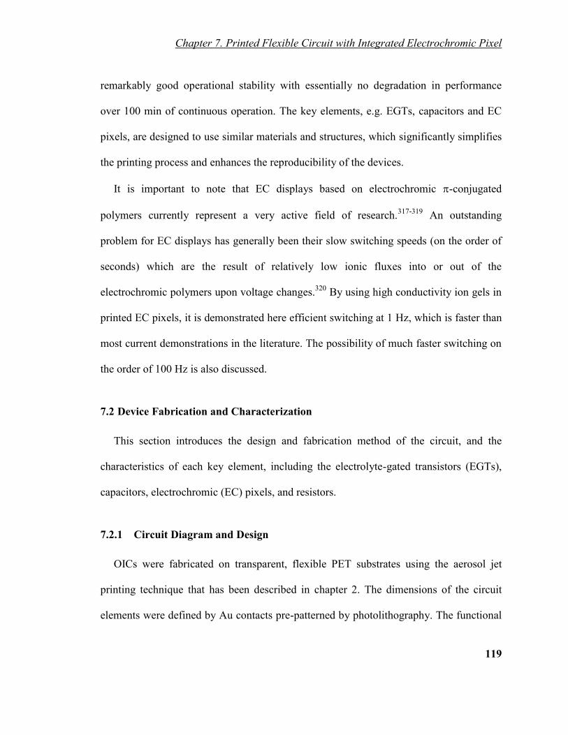
Chapter 7. Printed Flexible Circuit with Integrated Electrochromic Pixel
119
remarkably good operational stability with essentially no degradation in performance
over 100 min of continuous operation. The key elements, e.g. EGTs, capacitors and EC
pixels, are designed to use similar materials and structures, which significantly simplifies
the printing process and enhances the reproducibility of the devices.
It is important to note that EC displays based on electrochromic -conjugated
polymers currently represent a very active field of research.317-319
An outstanding
problem for EC displays has generally been their slow switching speeds (on the order of
seconds) which are the result of relatively low ionic fluxes into or out of the
electrochromic polymers upon voltage changes.320
By using high conductivity ion gels in
printed EC pixels, it is demonstrated here efficient switching at 1 Hz, which is faster than
most current demonstrations in the literature. The possibility of much faster switching on
the order of 100 Hz is also discussed.
7.2 Device Fabrication and Characterization
This section introduces the design and fabrication method of the circuit, and the
characteristics of each key element, including the electrolyte-gated transistors (EGTs),
capacitors, electrochromic (EC) pixels, and resistors.
7.2.1 Circuit Diagram and Design
OICs were fabricated on transparent, flexible PET substrates using the aerosol jet
printing technique that has been described in chapter 2. The dimensions of the circuit
elements were defined by Au contacts pre-patterned by photolithography. The functional

Chapter 7. Printed Flexible Circuit with Integrated Electrochromic Pixel
120
materials were all printed. These materials included P3HT, the ion gel based on
[EMI][TFSA] and a matrix of the triblock copolymer PS-PMMA-PS, PEDOT:PSS,
metallic carbon nanotubes (m-CNTs), PMMA and Ag.
Figure 7.1 illustrates the design of the entire circuit, which is composed of 23 EGTs,
12 capacitors, 20 resistors and 9 crossovers. The three main components of the circuit,
are the pulse generator, pixel driver, and electrochromic display pixel. By applying an
input signal, the pulse generator, which includes 4 inverter chains and 3 NAND gates,
will generate two pulses. The input signal can be triggered by a function generator, or by
a switch connected to VDD. There are 3 stages of inverters in each chain. When the input
signal passes through an inverter stage, the pulse is flipped and delayed. The delay time
(tdelay) is a function of the RC time constant of the inverter. The more stages the signal has
passed, the more delay it has compared to the original input. NAND 1 combines the
signals after chain 1 and chain 2 (as labeled in Figure 7.1 b), and outputs a pulse signal,
the width of which is determined by the time difference between outputs of chain 1 and
chain 2. The pulse width is determined by n×tdelay, where n is the number of stages in
each inverter chain. This eliminates the effect of the input width, e.g. the duration of
pressing the switch, on the circuit output signal. Chain 3 and chain 4 generate a second
pulse signal in the same way, which is delayed in time compared to the first pulse. The
two separate pulses enter NAND 3 and leave as two pulses in sequence. Simply
increasing the number of inverter chains and NAND gates can increase the number of
pulses, i.e., 6 chains and 4 NANDs can generate 3 pulses and switch the display 3 times.

Chapter 7. Printed Flexible Circuit with Integrated Electrochromic Pixel
121
Figure 7.1 Printed, flexible circuit and electrochromic pixel based on ion gel and
P3HT. (a) Diagram of the driving circuit. (b) Circuit layout of single inverter chain. (c)
Optical photo of the printed circuit with a 2.5×2.5mm2 electrochromic display pixel on
a flexible PET substrate.
Before the pulses going into the EC pixel (represented by a capacitor in Figure 7.1a),
the pixel driver modulates the shape of pulses and boosts the current to drive the pixel
more efficiently. The output splits into two opposite signals V1 and V2 after the driver,
because the pixel requires that the drive bias has both polarities (+1 V and -1 V).
Figure 7.1 b shows the component level of the first inverter chain, i.e., inverter stage 1
to stage 3. A typical p-MOS inverter includes an EGT and a load resistor, R, which are in
series between ground and VDD. The input signal enters the gate electrode of the EGT,
and the output leaves from the node between the EGT and load resistor. In this
5 mm
3 mm
(b)
VDD
Input Inverter Chain 1 NAND 1
NAND 2
NAND 3
12
(a)
(c)
Pulse Generator Pixel Driver
1110
987
654
321
V1
V2
CR
TFT
Input
GND
VDD
Inverter Chain
to 4 & NAND 11 2 3
Circuit
Pixel
Inverter Chain 2
Inverter Chain 3
Inverter Chain 4
Chapter 7. Printed Flexible Circuit with Integrated Electrochromic Pixel
122
demonstration, an extra capacitor, C, is added between the VOUT of the inverter and VDD.
The capacitor influences the charging and discharging time, i.e., the RC time of each
stage. By controlling the size of the capacitance, the inverter stage delay time, tdelay, can
be easily adjusted, and thus the width of the output pulses. The load resistors in the circuit
have systematically decreasing resistance across individual delay chains. This gradient in
resistance improves pulse shape and reduces the power consumption. The optical image
of the drive circuit (2.5 cm× 2 cm) with an electrochromic display (2.5 mm× 2.5 mm)
printed on PET substrate is shown in Figure 7.1 c. The architecture and characteristics of
each key element of the circuit are discussed in following sections.
Figure 7.2 Diagram of printed circuit.
Input
NAND 1
NAND 2
NAND 3Ground
VDD
Pixel DriverPulse Generator
Display
160 k
80 k
80 k
40 k
20 k
20 k 10 k
10 k

Chapter 7. Printed Flexible Circuit with Integrated Electrochromic Pixel
123
The detailed circuit diagram of the full circuit is shown in Figure 7.2. The printed
circuit consists of three elements, a pulse generator, a pixel driver, and a display pixel.
Except for the last stage of the pixel driver, the EGTs are 25 m in length and 500 m in
width. To boost the output current, the last stage of the pixel driver employs an EGT with
25 m in length and 2000 m in width. The load resistor varies from 160 k to 10 k.
The sizes of resistors in each stage are carefully chosen to balance the power
consumption, switching speed, signal swing and shape. For example, large resistors in
pulse generator ensure low power consumption, and small resistors in pixel driver can
provide higher output current. The capacitance of load capacitors can be tuned by the
thickness of the P3HT layer. Printed circuit outputs two consecutive pulses to switch the
color of printed electrochromic pixel. The resistors and capacitors together control the
switching frequency of the EC pixel.
7.2.2 Printed EGTs
The printed P3HT EGTs in the drive circuit have channel lengths L= 25 m and
widths W = 500 m, except for the EGTs in the last stage of the pixel driver with channel
width of 2000 m to ensure high output current. Figure 7.3 a left panel displays the
stacked structure of an ion gel gated P3HT EGT. Source and drain electrodes and the
circuit interconnects were pre-patterned on the PET substrate. The printing sequence was
P3HT semiconductor, ion gel gate insulator, followed by PEDOT:PSS which served as
the gate electrode. The operating mechanism of EGTs is shown in the lower panel. Under

Chapter 7. Printed Flexible Circuit with Integrated Electrochromic Pixel
124
negative gate bias, [TFSA]- anions migrate to the ion gel/P3HT interface, where
electrochemical oxidation of P3HT polymer chains occurs. This switches the P3HT from
insulating (OFF state) to conductive (p-type ON state) and increases the drain current (ID)
of the EGT by 5 orders of magnitude (Figure 7.3 b). In electrolyte gated devices, it is
important to consider penetration of ions into the semiconductor if it is permeable. In this
case, P3HT is permeable to the ionic liquid [EMI][TFSA] and thus electrochemical
oxidation (hole doping) of the entire thickness of P3HT can occur if there is sufficient
time for electrochemical reaction and ion diffusion. Therefore, EGTs allow three
dimensional gating of ion-permeable semiconductors, and this in turn means very high
drive currents are possible. Importantly, the electrochemical oxidation process is
reversible, so that the device may be cycled between the ON and OFF states repeatedly.
At the ion gel/PEDOT:PSS interface, [EMI]+ cations can also penetrate into the
conductive polymer layer under negative bias, providing enough gate capacitance such
that the total series capacitance of the PEDOT/gel/P3HT stack remains very high.93,321
The electronic characteristics of the EGT were measured in an N2 environment and are
shown in Figure 7.3 b and c. The transfer curve in Figure 7.3 a was acquired with the gate
voltage (VG) sweeping from 0.8 V to −1.2 V and back, at 75 mV/s. The p-channel EGT
turned on at VG ≈0 V, at VD = −0.1 V (drain voltage) and the ON/OFF ratio was above
105. Since all the devices were printed in ambient air, during printing the P3HT film was
likely doped with oxygen. This resulted in slight p-doping of the P3HT layer and caused
the Vth to shift to positively.322,323
This air doping effect can lead to a non-desirable
leakage current at 0 V in the circuit. The printed devices were stored in rough vacuum (>

Chapter 7. Printed Flexible Circuit with Integrated Electrochromic Pixel
125
10-3
Torr) at room temperature for 2 days, in order to de-oxygenate the P3HT. Ideally,
printing in inert environment could eliminate this problem.
Figure 7.3 Printed ion gel gated P3HT EGTs. (a) The stacked layer structure of a
printed EGT. Lower panel illustrates the bias condition as the EGT in on- state. (b)
Transfer characteristics of a typical printed EGT. (c) Output characteristics of a typical
EGT.
The transfer I-V curves were also carefully measured with different VD bias, from −0.1
V to −1 V. The ON current increased with VD, while the turn-on voltage had weak
dependence on VD, as expected. The output curve in Figure 7.3 b shows clear linear and
saturation regimes. In saturation regime, the drain current increases slightly with drain
bias, which may be due to the non-uniform space profile of ions under large drain bias.
The photomicrograph of a printed EGT is shown in the inset of Figure 7.3 b.
The transfer curve shows that the hysteresis between the forward and backward sweep
is small, indicating that ion diffusion is not limiting at VG sweep rates of 75 mV/s.
Actually, it has been shown previously that P3HT EGTs can easily work at speeds of
(b)
200m
10-3
I D(A
)
10-5
10-7
10-9
10-11
−1VG (V)
0.0−0.5
VD= −0.1 VVD= −0.2 VVD= −0.3 VVD= −0.4 VVD= −1.0 V
VG=−1.2 V
−0.8 V
−1.0 V
0.0 V
(c)
I D(m
A)
-0.75
-0.5
-0.25
0
0VD (V)−1−0.5 −1.5
PEDOT: PSS
Ion Gel
P3HT
Drain Source
VG
VD
(a)

Chapter 7. Printed Flexible Circuit with Integrated Electrochromic Pixel
126
several hundred Hz.25
With a close look at the OFF-state current, one can see the drain
current in forward sweep is about 1 order of magnitude lower than the backward sweep,
which appears like a hysteresis. However, the mechanism of the hysteresis is the different
sources of the OFF-state currents in the forward and reverse sweep. The origin of the
OFF current in forward sweep is the transient current through the ion gel electrolyte. It
can be seen from the inset of Figure 7.3 b, a small part of the source and drain electrodes
are exposed to ion gel electrolyte. This interface effectively acts as a parasitic capacitor
(CP). When VG is sweeping, there is a small charging or discharging current due to this
parasitic capacitor, and the current can be estimated by I=CP×dVG/dt, where dVG/dt is the
sweeping speed of VG. For the metal/ion gel interface, CP is about 10 F/cm2.87
Given the
area of CP is about 200×100 m2, and the sweep rate is 75 mV/s, the transient current is
estimated to be 1.5×10⁻¹⁰
A, which matches with the experimental data in Figure 7.3 b.
This current can be reduced by optimizing the architecture, in particular minimizing the
ion gel/source and ion gel/drain overlaps. As to the backward sweep, the dominant factor
influencing the OFF current is the number of carriers remaining in the trap states in the
semiconductor. These traps are shallow enough so that the carriers can be extracted by a
slightly positive VG, e.g. >0.5 V. The OFF current of the consecutive forward sweep will
not be affected. Both forward and backward OFF currents are independent on VD bias,
indicating the static current through the ion gel electrolyte is very small.

Chapter 7. Printed Flexible Circuit with Integrated Electrochromic Pixel
127
7.2.3 Printed Capacitors
As mentioned above, the total delay time, n×tdelay, in a single delay chain determines
the width of the output pulse. The number of stages n is not flexible once the circuit
design is fixed. tdelay is a function of R and C, where R is determined by the load resistor,
and C is the capacitance of transistor. Neither of these two factors can be tuned freely in a
typical circuit.25
To solve this problem, an extra load capacitor is added in each stage of
the inverter, which can be independently varied without affecting the inverter’s
parameters. The larger the capacitor is, the longer it takes to charge and discharge, thus
longer tdelays can be achieved.
Figure 7.4 Printed ion gel/P3HT capacitors. (a) A photomicrograph and (b) cross
section of the printed capacitor.
Figure 7.4 a shows the photomicrograph of a capacitor (500 m × 200 m), which
dimension is defined by the bottom Au electrode. The cross-sectional view of the
capacitor is illustrated in Figure 7.4 b, where the P3HT and the ion gel serve as the

Chapter 7. Printed Flexible Circuit with Integrated Electrochromic Pixel
128
semiconductor and dielectric layer, respectively. The top electrode PEDOT:PSS connects
to VDD. The structure of the ion gel/P3HT capacitor is similar to a metal-insulator-
semiconductor (MIS) capacitor. Depending on the relative bias between the top and
bottom electrodes of the capacitor, P3HT can be electrochemically oxidized or re-
reduced, which is equivalent to the charging and discharging process of conventional
MIS capacitors. With thicker P3HT films, there is larger electrochemical charging
capacity, and thus higher capacitance can be achieved.
The capacitance is measured as a function of bias frequency in Figure 7.5 a. A DC
bias (0 V) superimposed with a 10 mV AC bias was applied to the PEDOT:PSS
electrode. Without the P3HT layer, the capacitor, which is only an ion gel layer
sandwiched in between the PEDOT:PSS and Au electrodes, displayed C-f behavior
typical of a double-layer capacitor (black curve).87
Capacitance exhibited a plateau of ~ 3
F/cm2 at f < 10
5 Hz. The large capacitance may result from a combination of electrical
double layer (EDL) formation at the Au/gel and PEDOT/gel interfaces. It may also reflect
redox processes in the PEDOT (so-called ‘pseudo-capacitance’). By adding 200 nm
P3HT layer into the capacitor, the capacitance at lower frequencies (<104 Hz) was
significantly enhanced (red curve). The capacitance boost appeared to be a strong
function of the bias frequency, because the lower frequencies allow electrochemical
oxidation to occur whereas high frequencies do not. The thickness of P3HT layer has
more impact at the capacitance in low frequency regime. For instance, at 50 Hz, the
capacitor with 200 nm P3HT exhibits 50 F/cm2, and the one with 300 nm P3HT

Chapter 7. Printed Flexible Circuit with Integrated Electrochromic Pixel
129
displays 80 F/cm2(green curve). For f > 10
5 Hz, capacitance decreased because EDL
formation and redox reaction was suppressed. At the highest frequencies, only the bulk
polarization of the ion gel contributes to the capacitance, which gives a capacitance that
is orders of magnitude smaller than EDL and pseudo-capacitance. In these two regimes,
because of the suppression of diffusion, P3HT thickness has no effect on the capacitance.
Figure 7.5 b shows the capacitance-voltage (C-V) characteristic of a capacitor with
200 nm P3HT. With V > −0.3 V, the capacitance is small and weakly dependent on V. As
the applied bias sweeps to more negative voltage, holes are injected into P3HT, and the
capacitance starts to increase. Comparing C-V under different frequency, it can be seen
that the capacitance goes up with lower frequency, consistent with discussions above.
The capacitance at 10 Hz, −1.5 V is about 200 F/cm2. The integrated circuits
demonstrated in this report majorly works in ≤1 Hz frequemcy.
Figure 7.5 Electrical characteristics of printed capacitor. (a) Capacitance-frequency
(C-F) characteristics of printed capacitors, comparing no P3HT layer (black), P3HT
layer of 200 nm (red) and 300 nm (green) in thickness, respectively. (b) Capacitance-
voltage (C-V) characteristics of the printed capacitor.
0
P3HT Thickness (nm)
600400200 800 1000
4
Cap
acitance (F
)
3
1
0
2
PEDOT:PSS
P3HT
Au
Ion GelV
(a)
(b)
(c)
(e)
10-4
10-5
10-6
10-7
106105104103102
Cap
acitance
(F
/cm
2)
Frequency (Hz)
no P3HT
200 nm P3HT
300 nm P3HT
-2
Dis
pla
cem
ent
Curr
en
t (A
)
-1
0
1
-1.5
Voltage (V)
0-0.5-1
no P3HT200 nm P3HT
Invert
er D
ela
y (s) 1
0.5
00
P3HT Thickness (nm)
600400200 800 1000
(g)(f )
200
m
(d) 250
Cap
acitance
(F
/cm
2)
200
150
100
50
0-1
Voltage (V)10
10 kHz
1 kHz
100 Hz
10 Hz
200 nm P3HT
Forward
Backward
VDD VOUT
500 m
0.5 1
Ion Diffusion EDLNo
EDLS
heet C
ap
acitance
(10
3F
/cm
2)
4
3
1
0
2
(a) (b)

Chapter 7. Printed Flexible Circuit with Integrated Electrochromic Pixel
130
The quasi-static capacitance measured by displacement current is illustrated in Figure
7.6. The charging and discharging current was measured when voltage was swept in
2.86V/s from 1.5V to -1.5V and backward. The 200 nm P3HT capacitor (red curve)
showed much higher current comparing to the capacitor without P3HT (black curve).
Integration of the shadow area gives a capacitance difference of 520 F/cm2. Since the
whole sweep takes about 1 s, this capacitance value can be considered similar as under 1
Hz bias.
Figure 7.6 Displacement current of capacitors with and without P3HT layer. By
integrating the shaded area, the effective capacitance is estimated to be 500 F/cm2.
Voltage is swept at 2.86 V/s.
When the circuit is operating, neither voltage nor frequency is static, which means the
real capacitance is changing with time. In order to characterize the effective capacitance
of the ion gel-gated P3HT capacitor in the drive circuit, and its impact on the average
delay time, tdelay was measured as a function of P3HT thickness and shown in Figure 7.7
a. tdelay, was measured from the time difference between the rising edges of two
0
P3HT Thickness (nm)
600400200 800 1000
4
Cap
acitance (F
)
3
1
0
2
PEDOT:PSS
P3HT
Au
Ion GelV
(a)
(b)
(c)
(e)
10-4
10-5
10-6
10-7
106105104103102
Cap
acitance
(F
/cm
2)
Frequency (Hz)
no P3HT
200 nm P3HT
300 nm P3HT
-2
Dis
pla
cem
ent
Curr
en
t (A
)
-1
0
1
-1.5
Voltage (V)
0-0.5-1
no P3HT200 nm P3HT
Invert
er D
ela
y (s) 1
0.5
00
P3HT Thickness (nm)
600400200 800 1000
(g)(f )
200
m
(d) 250
Cap
acitance
(F
/cm
2)
200
150
100
50
0-1
Voltage (V)10
10 kHz
1 kHz
100 Hz
10 Hz
200 nm P3HT
Forward
Backward
VDD VOUT
500 m
0.5 1
Ion Diffusion EDLNo
EDL
Sh
eet C
ap
acitance
(10
3F
/cm
2)
4
3
1
0
2

Chapter 7. Printed Flexible Circuit with Integrated Electrochromic Pixel
131
consecutive odd or even inverter stages. Each data point of tdelay shown in Figure 7.7 a
was averaged based on 12 inverters, where the EGTs and load resistors were the same.
tdelay for P3HT=0 nm was acquired from the inverter without load capacitors. The P3HT
layer thicknesses were varied from 156 nm to 944 nm in the load capacitors, which
resulted in tdelay increasing from 0.3 s to 1.1 s. The change of tdelay showed a transition
from linear to a saturation regime around 400 nm. The thickness of the P3HT layer in
capacitors can be designed based on desired delay time and pulse width.
Figure 7.7 Impact on delay time and effective capacitance of printed capacitors. (a)
Delay time of the inverters with loaded capacitors. (b) Effective capacitance of the
load capacitor estimated from delay time as a function of P3HT thickness. Estimation
is based on t=ln2×RC.
It is worth noting that tdelay in Figure 7.7 a may not be quantitatively compared to the
time constant of C-F measurement in Figure 7.5 a, since the charging current in Figure
7.7 a is limited by the inverter EGT, and the current in Figure 7.5 a is limited by the
impedance of the impedance analyzer. Figure 7.5 b shows the effective capacitance of the
capacitor is up to 3.7 F at 944 nm, corresponding to a sheet capacitance of 3700 F/cm2.
0
P3HT Thickness (nm)
600400200 800 1000
4
Cap
acitance (F
)3
1
0
2
PEDOT:PSS
P3HT
Au
Ion GelV
(a)
(b)
(c)
(e)
10-4
10-5
10-6
10-7
106105104103102
Cap
acitance
(F
/cm
2)
Frequency (Hz)
no P3HT
200 nm P3HT
300 nm P3HT
-2
Dis
pla
cem
ent
Curr
en
t (A
)
-1
0
1
-1.5
Voltage (V)
0-0.5-1
no P3HT200 nm P3HT
Invert
er D
ela
y (s) 1
0.5
00
P3HT Thickness (nm)
600400200 800 1000
(g)(f )
200
m
(d) 250
Cap
acitance
(F
/cm
2)
200
150
100
50
0-1
Voltage (V)10
10 kHz
1 kHz
100 Hz
10 Hz
200 nm P3HT
Forward
Backward
VDD VOUT
500 m
0.5 1
Ion Diffusion EDLNo
EDL
Sh
eet C
ap
acitance
(10
3F
/cm
2)
4
3
1
0
2
(a) (b)

Chapter 7. Printed Flexible Circuit with Integrated Electrochromic Pixel
132
The effective capacitance is estimated based on tdelay(x nm) − tdelay(0 nm)=Ln2×RC, where
R=160 k is the resistance of the load resistor in the inverter chains.
The ion gel/P3HT capacitor is characterized by several different measurements. All
measurements demonstrate the capacitance is a function of the P3HT thickness. It is note-
worthy that, unlike a conventional MIS capacitor, the capacitance does not depend on the
thickness of ion gel (dielectric). The capacitance of ion gel/P3HT capacitor depends on
P3HT thickness, bias voltage and frequency. Thicker P3HT, higher bias, and lower
frequency lead to larger capacitance.
7.2.4 Printed EC Pixel
The conjugated polymers PEDOT:PSS and P3HT are also known to be electrochromic
materials with good chemical stability.15,104,324
PEDOT:PSS is blue in the pristine or
semi-oxidized state, and transparent when further oxidized (fully conducting). P3HT has
a red-purple color in the neutral state and is a translucent blue when oxidized. This
section shows a bi-color printed electrochromic pixel based on the ion gel, P3HT and
PEDOT:PSS. The structure is very similar as the capacitor discussed in previous section,
except the bottom Au electrode is replaced by a transparent printed metallic CNTs thin
film. The PEDOT:PSS layer also serves as the second electrode due to its large
conductance (up to 1000 S/cm). The device switches from reddish purple to blue
reversibly.
Figure 7.8 illustrates the change of the UV-visible absorption spectra of a stand-alone
EC pixel under various voltage biases. The spectra were acquired in ambient air. The EC

Chapter 7. Printed Flexible Circuit with Integrated Electrochromic Pixel
133
Pixel was illuminated with light at fixed wavelengths and the transmitted intensity was
measured. The bottom metallic CNT electrode was grounded and the bias voltage was
applied on the PEDOT:PSS layer at 1.5 V, 0 V, and −1 V, respectively. At 0 V (purple
curve), the spectrum shows two broad absorption peaks of the EC pixel: one at the green
wavelength region (around 530 nm), and the other one at the red to infrared region (a
broad absorption around 850 nm). The positions of the two peaks are close to the reported
absorption spectra of the pristine P3HT and PEDOT:PSS, respectively.15,325,326
At
positive bias, with [TFSA]− anions diffusing in, the PEDOT:PSS layer was further
oxidized compared to the 0 V condition. The absorption of the red wavelength was
largely suppressed (pink curve), and PEDOT:PSS turned into transparent state. On the
other side of the electrolyte, P3HT was further reduced compared to 0 V. Since the P3HT
is slightly p-doped with air exposure, a slightly positive bias brings the P3HT to pristine
state (similar as the “OFF state” as in EGTs). As a result, the stronger green absorption
(around 530 nm) can be seen comparing to 0 V. The EC pixel appeared to be purple-red
at 1.5 V, as shown in the left image in Figure 7.8.
At negative bias, PEDOT:PSS was reduced, and P3HT was oxidized. The EC pixel
absorbed more at the red wavelength, and less at green wavelength, hence the EC pixel
showed a blue color at −1 V, as shown in the right image of Figure 7.8. The transmitted
light intensity is measured and subtracted by the background and normalized to the
highest peak. The change of the spectra represents the change in bulk of P3HT and
PEDOT:PSS polymer layers, which again illustrated the 3D ion diffusion and is
consistent with the discussions in EGT and capacitor section.

Chapter 7. Printed Flexible Circuit with Integrated Electrochromic Pixel
134
Figure 7.8 Printed EC pixel. UV-vis absorption spectra of printed pixel under various
voltage biases is shown. The inset shows the color contrast of the pixel as a function of
bias frequency.
The ion gel contains only 20 wt% of triblock copolymers, thus the ion motion is
weakly affected by the polymer chains and can potentially enhance the switching speed
of the pixel. To measure the dynamic response of the printed EC pixel, the m-CNT
electrode was grounded, while a square wave signal with controlled frequency was
applied to the PEDOT:PSS electrode of the pixel. A laser was set to 530 nm and 800 nm,
and the transmitted light intensity was transformed to voltage signal. The voltage
modulation on the transmission at 1 Hz is shown in Figure 7.9. Pink curve illustrates the
change of the transmission at 530 nm (reflecting the change of P3HT absorption), which
reached the maximum at V = −1.5 V and minimum at V = 1.5 V. The transmission at 800
nm (reflecting the change of PEDOT:PSS absorption), shown in the blue curve, was also
modulated by voltage but in the counter direction of P3HT curve. The transmitted signal
(a)
Ab
so
rptio
n
(Arb
itra
ry U
nit)
0.0
0.5
1.0
400 600 800 1000
Wavelength (nm)
1.5 V
0 V
-1 V
Vo
lta
ge
(V
)
Tra
nsm
issio
n
(Arb
itra
ry U
nit)
0.0
0.5
1.0
-2
0
2
0.0
0.5
1.0
Input
530 nm
800 nm
0 1 2 3
Time (s)
4 5
Co
ntr
ast
(Arb
itra
ry U
nit)
0.4
0.8
1.0
0.1 1 10Frequency (Hz)
800 nm
530 nm
0.6
(b)

Chapter 7. Printed Flexible Circuit with Integrated Electrochromic Pixel
135
followed the modulating voltage signal, indicating the EC pixel can fully switch color at
1 Hz. The unit of transmission was subtracted by the background and normalized to the
highest peak. Note here the way the transmission modulated by the bias is in the opposite
direction comparing the absorption spectrum in Figure 7.8.
Figure 7.9 Dynamic optical response of the printed EC pixel under 1 Hz bias.
In addition, the color contrast was measured as a function of the bias frequency,
shown in the inset of the Figure 7.8a. At each wavelength, the intensity change of the
transmitted light was measured at various voltage frequencies (0.25 Hz – 20 Hz), and
normalized to the change at 0.25 Hz. The EC pixel remained full contrast up to 5 Hz, and
the contrast started to decrease above 10 Hz. When operating at 20 Hz, the pixel
remained 60% contrast. Comparing to EGT and capacitors, the EC pixel seems to be
“slower”. This is because the color contrast is more sensitive to the ion diffusion depth.
(a)
Ab
so
rptio
n
(Arb
itra
ry U
nit)
0.0
0.5
1.0
400 600 800 1000
Wavelength (nm)
1.5 V
0 V
-1 V
Vo
lta
ge
(V
)
Tra
nsm
issio
n
(Arb
itra
ry U
nit)
0.0
0.5
1.0
-2
0
2
0.0
0.5
1.0
Input
530 nm
800 nm
0 1 2 3
Time (s)
4 5
Co
ntr
ast
(Arb
itra
ry U
nit)
0.4
0.8
1.0
0.1 1 10Frequency (Hz)
800 nm
530 nm
0.6
(b)

Chapter 7. Printed Flexible Circuit with Integrated Electrochromic Pixel
136
Full color contrast requires the electrochromic layer to be completed doped with ions. At
higher frequencies, the diffusion depth of ions is limited, thus only part of the film
changes color and results in the lower color contrast. On the contrary, ion diffusion in ion
gel gated EGT is an enhancement to the current and capacitance, but not a requirement of
the functionality. Therefore, those devices can function at a frequency up to kHz.
However, there is room for further optimization of switching speed of printed EC pixel,
including device architecture, electrochromic film thickness, electrode conductivity, etc.
7.2.5 Printed Resistors and Crossovers
In p-MOS logic circuit, the load resistor controls the output swing and trip point of an
inverter. The load resistors in inverter chains are large enough (160 k to provide
enough delay time and reduce the power consumption. Resistors in NAND 1 and 2 are 80
k, and in NAND 3 is 40 k. The pixel driver employs 20 k and 10 k (last stage),
respectively. There are two advantages of using this gradient profile of resistance design.
First, it gradually regulates the shape of the falling and rising edge of each stage, so that
the last stage outputs a high current and square wave to drive the pixel (see discussion in
section 7.3). Meanwhile, it minimizes the power of the whole circuit. As demonstrated in
the inset of Figure 7.10 a, a strip of PEDOT:PSS is printed between two patterned Au
contacts which fixed the length of the resistor. The resistance depends on the thickness
and width of the PEDOT:PSS strip, and can be controlled by the printing speed and
number of loops. Figure 7.10 a shows the I-V characteristics of a typical resistor in
NAND 1 and 2, and the nice linear characteristic indicates ohmic contact between the

Chapter 7. Printed Flexible Circuit with Integrated Electrochromic Pixel
137
printed PEDOT:PSS stripe and Au pads. A crossover, similar to the via in silicon
circuitry, connects two wires without shorting to others. As shown in the inset of Figure
7.10 b, a PMMA thin film was printed as a cover for the two vertical Au lines, and a
silver line was printed on top connecting the two horizontal Au lines. The crossovers
should be much smaller in resistance compared to other elements in the circuit to avoid
undesired voltage drops. Therefore, silver was employed due to its high conductance. The
resistance of the silver line was ~ 8 , as assessed from the I-V curve shown in Figure
7.10 b.
Figure 7.10 I-V characteristics of printed resistor and crossovers. (a) The I-V curve of
a printed PEDOT:PSS resistor (red open circle), which serves as a load resistor in the
NAND 1 or NAND 2. The resistance estimated from the slope is ~ 82 k. (b) The I-V
curve of a printed crossover (red open circle), which resistance is estimated to be 8
based on the slope. Inset shows that a thin film of PMMA is printed on top of two
vertical Au lines as an insulator, and a silver line is printed on top of the PMMA
connecting the two horizontal lines.
R=8 R=82 k
200m 200m
30
20
10
0
-10
-20
-30-2 -1 0 1 2
Cu
rre
nt (
A)
Voltage (V)
30
20
10
0
-10
-20
-30
Cu
rre
nt (m
A)
-0.2 -0.1 0.0 0.1 0.2Voltage (V)
(a) (b)

Chapter 7. Printed Flexible Circuit with Integrated Electrochromic Pixel
138
7.3 Printed Circuit Performance
Pulse generator consists of 12 stages of inverters. When signal passing through a stage
of inverter, it is flipped and delayed. Figure 7.11 (a) illustrates the function of an inverter,
measured in an inverter with a load resistor of 160 k, without the load capacitor, at
VDD= −1 V. When input is 0 V, the inverter outputs −1 V, while the input sweeps to −1
V, output is flipped to 0 V.
Figure 7.11 Inverter and signal flow in delay chains. (a) The input-output
characteristics of a printed ion gel inverter at VDD= −1 V. (b) Voltage signal in
inverter chains.
Each stage delays the signal in time due to the RC time of the inverter. Figure 7.11 (b)
shows the output voltage signal as a function of time from stage 2 to 12, after triggered
by the input (black). It can be seen the even stages and odd stages have opposite pulses,
also the rising and falling edges of the signals are not symmetric. This is because at the
rising edge, the dominant current is the on-state current of the EGT, about mA. While at
VIN (V)
VO
UT
(V)
-1
-1.0
-0.5
-0.5
0
0.0
Stage 2
3
12
4
5
6
8
7
9
10
11
Input
0 2 4 6 8Time (s)
Vo
lta
ge
(U
nit 1
V)
∆t
(a) (b)VDD = -1 V VDD = -1 V

Chapter 7. Printed Flexible Circuit with Integrated Electrochromic Pixel
139
the falling edge, the dominant current is from the load resistor (VDD/Rload), about 10 A.
The larger current leads to shorter charging time and fast switching edge. Hence the
falling edge is always slower than the rising edge in inverter chains.
In typical silicon circuits, the delay time of an inverter is measured from the middle of
input rising edge, to the middle of the output falling edge. In this case, the asymmetry
edges introduce the inaccuracy in such measurement. Thus the average delay time of the
inverter is measured between the two rising edges of consecutive odd stages or even
stages. As an example, the time difference (∆t) between stage 10 and stage 12 is shown in
shaded area in Figure 7.11 (b). Stage 11 and stage 12 both contribute to ∆t, hence ∆t
=2×tdelay, where tdelay is the average delay time of an inverter.
Another issue raised by the asymmetric rising and falling edges is the total delay time
of the odd and even inverter chains are different, although all chains have 3 stage of
inverters. Since the falling time is much longer than the rising time, therefore, the major
contribution to the total delay time of an inverter chain comes from the falling edges. In
even inverter chain, e.g. chain 2, from stage 4 to 6, there are two falling edges and one
rising edge, while in odd chain, e.g. chain 3, from stage 7 to 9, there are only one falling
edge and two rising edges, as shown in Figure 7.11 (b). This means the total delay time of
odd chains are smaller than the even chains.
When all the signals are combined by NAND 3, the differences of the delay time can
be seen clearly. Figure 7.12 demonstrates the effect discussed above. NAND 3 outputs
two consecutive pulses, and the width of the pulse is not determined by the input, but the

Chapter 7. Printed Flexible Circuit with Integrated Electrochromic Pixel
140
delay time from chain 1 – 4, as illustrated by the dashed lines. Clearly, t1 and t3 are
shorter comparing to t2 and t4. To solve this problem, the capacitors in odd inverter chains
are doubled to compensate the difference. An alternative solution could be adding two
more stages in odd chains.
NAND 3 employs load resistor of 40 k. The small load resistance decreases the
falling time of the output. Therefore, the pink curve shows more symmetric rising and
falling edges. The gradient change profile of the load resistors from inverter chains,
NANDs, to drivers, regulates the shape of the output signal. At the final stage, the output
is modulated as a well defined square wave function as shown in Figure 7.13.
Figure 7.12 Output of NAND 3.
Integrating all the key elements together, an EC pixel driver circuit generating two
pulses to switch the pixel color is demonstrated. Since the pixel requires both polarities to
switch it, two outputs are designed in opposite waveform, as shown in Figure 7.13. With
0 2 4 6 8Time (s)
Vo
lta
ge
(U
nit 1
V) Stage 3
Input
Stage 6
Stage 9
Stage 12
NAND 3
VDD = -1 V
t1 t2 t3 t4

Chapter 7. Printed Flexible Circuit with Integrated Electrochromic Pixel
141
an input trigger (black), the outputs showed uniformly shaped square waves with
opposite signs, where t1 to t4 are the delay times from inverter chains 1 to 4. The evenly
distributed outputs demonstrate good control in the printing process as well as the
modulation and circuit design.
Figure 7.13 The output performance of the printed circuit.
Output 1 and output 2 (as labeled in Figure 7.1 b) are connected to the PEDOT:PSS
electrode and m-CNT electrode of the pixel, respectively. When VOUT 1= 0 V and VOUT 2
= −1 V, the pixel is effectively under 1 V bias and displays a reddish purple color. With
VOUT 1= −1 V and VOUT 2 = 0 V there is an effective bias of −1 V which switches the
pixel to blue. The color of the display pixel switched twice upon every input pulse. The
drive pulse widths were designed to be 2 s (0.5 Hz), in order to reach the maximized
color contrast of the pixel.
Efficient switching of large EC pixels requires very large charge, hence high output
current is the key to achieving fast switching and high color contrast. The printed circuit
0
Vo
ltag
e (V
) -1
0
-1
0
(a)
-1
0
Time (s)
42 86
Input
VOUT 1
VOUT 2
no display
1 mm2
2 mm2
6 mm2
Vo
ltag
e (V
)
-1
0
(b)
0
Time (s)
4 86
0 min10 20 30 40
50
60 70 80 90100
2 4 86
Time (s)
Vo
ltag
e (V
)
-1
0
(c)
t 1 t 2 t 3 t 4

Chapter 7. Printed Flexible Circuit with Integrated Electrochromic Pixel
142
was tested with EC pixels of different sizes, from 1 mm2 to 6 mm
2. A magnified view of
one pulse is shown in Figure 7.14. The 1 mm2 and 2 mm
2 pixels had no obvious effects
on the output signal, while the 6 mm2 one slightly slowed down the falling edge of the
signal, indicating it takes longer time to switch larger pixel. In essence, the pixel
functions the same way as a load capacitor does, i.e., the capacitance and charging time
increases proportional to the area. To retain the same performance, the driving current
should be proportional to the pixel size. Some simple strategies can be employed in the
circuit design if larger size pixels are desired, such as increasing the EGT channel W/L
ratio and decreasing the resistance of the load resistors in the driving unit.
Figure 7.14 Capacity of the driving circuit. Pixel in 1 mm2 and 2 mm
2 can be driven
without affecting the circuit outputs. Pixel in 6 mm2 deforms the output waveform
slightly due to the long charging time.
A good operational stability of the printed circuit was demonstrated. A circuit without
a load pixel was tested for 100 minutes in N2 continuously, with VDD = −1 V and an input
pulse every 10 s. Output 1 was recorded every 10 minutes, from 0 to 100 min, as shown
0V
oltag
e (V
) -1
0
-1
0
(a)
-1
0
Time (s)
42 86
Input
VOUT 1
VOUT 2
no display
1 mm2
2 mm2
6 mm2
Vo
ltag
e (V
)
-1
0
(b)
0
Time (s)
4 86
0 min10 20 30 40
50
60 70 80 90100
2 4 86
Time (s)
Vo
ltag
e (V
)
-1
0
(c)
t 1 t 2 t 3 t 4

Chapter 7. Printed Flexible Circuit with Integrated Electrochromic Pixel
143
in Figure 7.15. The output signal showed excellent stability over 100 min, 600 cycles,
with no degradation in amplitude and only minor shift in position.
Figure 7.15 Operational stability of printed circuit. VOUT 1 was tested continuously
for 100 minutes, 600 cycles continuously, in N2, showing no degradation in output
swing, only slightly shifting in time.
7.4 Conclusions
In summary, all key components of the drive circuitry, namely resistors, capacitors,
and transistors, were aerosol jet printed onto a plastic foil; metallic electrodes and
interconnects were the only components pre-patterned on the plastic by conventional
photolithography. The large milliamp drive currents necessary to switch a 4 mm2 EC
pixel were controlled by printed EGTs that incorporate printable ion gels for the gate
insulator layers and P3HT for the semiconductor channels. Upon application of a low
voltage input pulse, the circuit switches the printed EC pixel ON (red) and OFF (blue)
two times in approximately 4 seconds. The high capacitance ensures the high output
0
Vo
ltag
e (V
) -1
0
-1
0
(a)
-1
0
Time (s)
42 86
Input
VOUT 1
VOUT 2
no display
1 mm2
2 mm2
6 mm2
Vo
ltag
e (V
)
-1
0
(b)
0
Time (s)
4 86
0 min10 20 30 40
50
60 70 80 90100
2 4 86
Time (s)
Vo
ltag
e (V
)
-1
0
(c)
t 1 t 2 t 3 t 4

Chapter 7. Printed Flexible Circuit with Integrated Electrochromic Pixel
144
current of EGTs (>1 mA), the high capacitance of ion gel-gated P3HT capacitors (> 100
F/cm2), as well as the fast switching speed of the display pixels (up to 20 Hz). The key
elements, EGTs, capacitors and pixels are all based on P3HT, ion gel, and PEDOT:PSS,
in similar layered structure and can be fabricated in simple printing process. The good
control of printing process and reliable device performance ensure the using of
conventional software on circuit design and simulations. The printed circuit drives the
display to full contrast at 1 V supply voltage, and showed good stability up to 600 cycles,
which demonstrate a great potential of the printed electronics in low voltage, portable
applications. This is the most sophisticated circuit reported to date based on EGTs and it
also demonstrates that complex materials integration can be achieved with a simple
printing process.

Chapter 8. Future Research
145
Future Research Chapter 8
Chapter 5-7 summarize the experimental work of electrolyte-gated transistors (EGTs),
circuits and their applications in printed circuits. This chapter discusses the remaining
challenges and opportunities for future research.
8.1 Power Consumption of Printed Circuits*
When considering the applications in portable electronics, low supply voltage, as what
has been discussed extensively in previous chapters, is a key factor in circuit design. In
addition to it, low power consumption is also strongly desired. Both low voltage and low
power need to be achieved in order for the electronics to be compatible with flexible
batteries and light weight applications. In conventional silicon technology,
complementary metal-oxide-semiconductor (CMOS) circuits can achieve much lower
power consumption compared to n channel (i.e., NMOS) or p channel (i.e., PMOS) only
circuits. CMOS consists of both n channel and p channel MOSFETs. At any moment of
the steady state, one FET of the pair is in the OFF state, therefore, very little static power
is consumed. The power consumption only occurs during the switching status. On the
other hand, NMOS (or PMOS) only logic circuits are implemented by FETs and resistors.
There is a high static current goes through the resistor even when the transistor is in OFF
state, which results in a high static power consumption. Besides the lower power, CMOS
* Reproduced in part with permission from Ha, M., Xia, Y., Green, A. A., Zhang, W., Renn, M. J., Kim,
C.H., Hersam, M. C., Frisbie, C. D., ACS Nano, 4, 4388-4395 (2010). Copyright 2010 American Chemical
Society.

Chapter 8. Future Research
146
also offers higher density of logic functions and higher noise margin. Hence, CMOS
circuit is the most used circuit in VLSI (very-large-scale integration) chips.
In printed circuitry, complementary circuit remains challenging. A major challenge is
the material and processing of n type semiconductors. Organic n type materials are rare
and usually sensitive to oxygen and water.328
These make the high performance n channel
transistors very difficult to fabricate. Intensive studies are trying to understand the
reasons behind the differences of p type and n type organic semiconductors, the design
rules of the high performance, stable n type semiconductors, the synthesis and fabrication
of materials and devices.274,277,309,329
However, this is still an area needed a breakthrough.
As what have been demonstrated in previous chapters, semiconducting CNT is a great
candidate of fast, low voltage, printable circuits, however, it is worth noting that the
power consumption in this type of circuits may not be an advantage. Using ambipolar
transistors, the printed CNT circuit has unique characteristics. Unlike the PMOS or
NMOS circuits, the ambipolar circuit has no resistor which leads to a fixed static current.
However, the ambipolar circuit also cannot achieve the power consumption as low as
CMOS circuit, since the transistor may not be turned OFF due to its nature.
The modeling of the power consumption of CNT ring oscillators is collaborated with
Prof. Chris. H. Kim group. The ambipolar CNT EGT is modeled as an NMOS and a
PMOS transistor connected in parallel, with the same channel length (50 m) and width
(500 m). The Hspice Level 3 silicon empirical model was used, and the model
parameters were adjusted to fit the data. From Figure 8.1, it can be seen that the model

Chapter 8. Future Research
147
fits the experimental ID-VG data well. The mobilities of the NMOS and PMOS transistors
are set to be 20 and 80 cm2/Vs, and the threshold voltages are set at 0.72 and -0.3 V,
respectively. With this compact model, the inverter behavior was verified through
simulation, and optimization of inverter design is possible.
Figure 8.1 c and d demonstrate that the model can be employed to understand the
switching mechanism of ambipolar CNT inverters. The current of the inverter shows a
minimum around the transition point, which means the ambipolar inverter operates
differently than a conventional CMOS inverter in which current is peaked at the
transition voltage. Figure 8.1 d shows the currents of the n- and p- channels in our model,
as a function of VIN. With VIN close to VDD (1.5 V), the current from the n-channel of EGT
a (blue straight line) is higher than that of the p-channel (red straight line), indicating
EGT a works in the n-type regime. For the same reason (dashed lines), EGT b also works
as n-type. Similarly, when VIN is close to ground (0 V), both transistors a and b will work
in p-type mode. A key point is that the bias conditions for the two EGTs are different;
therefore, the functionality of the inverter can be realized. However, only within a small
voltage regime around the transition point (VIN ~ 1 V) does the ambipolar inverter work
similarly to a classic complementary inverter, where EGT a is p-type and EGT b is n-
type.
Since the two transistors are both in the ON state, the static power dissipation in
ambipolar inverters is expected to be higher than in CMOS circuits. It can be estimated,
Pstatic = IVDD as the average of power consumed at VIN = 1.5 V and 0 V. The currents at

Chapter 8. Future Research
148
1.5 V and 0 V are 0.2 mA and 2 mA (not shown), respectively, with VDD = 1.5 V.
Therefore, average Pstatic is about 1.6 mW.
Figure 8.1 The simulations of the ambipolar CNT EGTs and inverters. (a), The
equivalent circuit which is used to simulate the CNT inverters. Each CNT EGT is
modeled as a p- and an n-channel in parallel. (b), The transfer curves of the simulated
and experimental ambipolar CNT EGT. Open circles show the experimental results,
with VD= 0.1 V (black) and -1 V (red); straight lines show the simulated curves, with
VD= 0.1 V (black) and -1 V (red). (c), The drain currents of a printed CNT inverter
from experiments (black open circles) and simulation (black solid circles), and the
output voltage characteristics from experiments (red open circles) and simulation (red
solid circles), respectively. VDD=1.5 V. (d), Simulated currents of the p channel of
EGT a (red straight line), n channel of EGT a (blue straight line), p channel of EGT b
(red dashed line), and n channel of EGT b (blue dashed line).

Chapter 8. Future Research
149
The dynamic power dissipation per stage of the CNT ring oscillator can be estimated
as Pdynamic= CVDD2f = 50 W, where C is the total capacitance calculated below (Figure
5.10) as 4 nF, VDD is 2.5V and f is 1.9 kHz, as shown in Figure 5.8c. Note that for the
ambipolar CNT ring oscillator Pdynamic< Pstatic, which is the opposite of the situation for
conventional complementary ring oscillators.
Based on above analysis, it is clear why ambipolar circuit may have high power
consumptions. However, semiconducting CNT still has incredible merits of printable
electronics, such as the very high mobility, chemistry stability and the compatibility to air
processing. Here, a few strategies are proposed for the further improvements in
considerations of power consumptions.
8.1.1 Modification of the Electrolyte Material.
The ion gel electrolyte employed in this thesis is based on ionic liquids which have
high ionic conductivities for both cations and anions. Berggren’s group demonstrated
polyelectrolyte materials consists of cations and anions with different sizes, where only
smaller ions are mobile. By selecting appropriate polyelectrolyte, the printed CNT
transistor may behave as n-type transistor if only cations in the polyelectrolyte are
mobile, or p-type if anions are mobile. A true CMOS circuit can be achieved by
implementing two kinds of electrolyte into the circuits, without any changes to the
semiconducting material. Hence, both the high performance of circuit and low power are
possible.

Chapter 8. Future Research
150
8.1.2 Modification of Semiconducting CNTs.
Although the semiconducting CNTs are intrinsic ambipolar, the band gap of the CNTs
are actually tunable, thus the characteristics of p-type and n-type transport. As introduced
in Chapter 3, the band gap of CNTs is inversely related to the nanotube diameters (Figure
3.4). Smaller diameters lead to higher energy gap, which means the difference between
electron and hole transport energy levels is larger. In other words, the threshold voltages
for electrons and holes move further apart, as in Figure 8.2. With smaller diameter (black
curve), the ON and OFF current of the transistor remains the same as larger diameter
nanotubes (red curve), but the OFF regime is wider. This may help to reduce the static
current in ambipolar circuits. This strategy is relatively easy since the selection based on
nanotubes diameter is possible as discussed in Chapter 3.
Figure 8.2 Transfer characteristics of transistors based on CNTs with different
diameters. Left panel is in semi-log scale, and right panel in linear scale.
-1 0 1 210
-9
10-8
10-7
10-6
10-5
10-4
I (A
)
VG (V)
lager diameter CNT
smaller diameter CNT
-1 0 1 20
25
50
I (
A)
VG (V)
larger diameter CNT
smaller diameter CNT
OFF
regime
VOFF

Chapter 8. Future Research
151
Other options remains open, including doping the intrinsic semiconducting CNTs to
be p-type and n-type, making more sophisticate circuit design to compensate the
undesired static current, etc., but they may lead to topics beyond optimizing the device
architecture and will not be discussed in details.
8.2 Capacitor with Large Capacitance and Its Applications
Ion gel provides large surface capacitances because of the formation of the electric
double layer. As discussed in previous chapters and in literatures, ion gel gated transistors
(based on CNTs, organic crystals, polymers, etc.) were demonstrated with low voltage,
enhanced mobilities or ON/OFF ratios, thanks to the high sheet capacitance. In fact, the
capacitance itself may lead to interesting researches and applications.
Chapter 7 shows the ion gel capacitors can be integrated into the driving circuit of the
electrochromic pixel. Besides the application in logic circuits, large capacitor is also
attractive in areas such as batteries and storage. Collaborating with Prof. Kim, we have
demonstrated a dynamic random-access memory (DRAM) array based on printed ion gel-
gated transistors, which is briefly described as following.12
The individual DRAM cell consists of three printed ion gel-gated transistors. The
circuit diagram is shown in Figure 8.3 (a). Although there is only single type of
transistors in this type of circuit, which is commonly referred as gain cells, the static
current can be ignored. The major challenge of the gain cells is the “retention time” (the
duration of information can be stored without refreshing) is typically low, e.g., ~ 100 s
in modern silicon technology. In this design, an ion gel-gated transistor is used as the
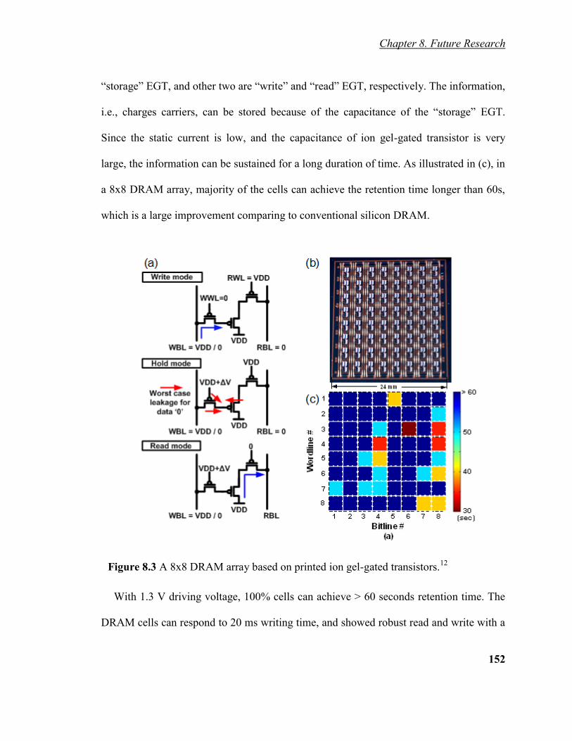
Chapter 8. Future Research
152
“storage” EGT, and other two are “write” and “read” EGT, respectively. The information,
i.e., charges carriers, can be stored because of the capacitance of the “storage” EGT.
Since the static current is low, and the capacitance of ion gel-gated transistor is very
large, the information can be sustained for a long duration of time. As illustrated in (c), in
a 8x8 DRAM array, majority of the cells can achieve the retention time longer than 60s,
which is a large improvement comparing to conventional silicon DRAM.
Figure 8.3 A 8x8 DRAM array based on printed ion gel-gated transistors.12
With 1.3 V driving voltage, 100% cells can achieve > 60 seconds retention time. The
DRAM cells can respond to 20 ms writing time, and showed robust read and write with a

Chapter 8. Future Research
153
supply voltage down to 0.8 V. In addition, the static power consumption of this circuit is
only about 10 nW, which is orders of magnitude lower than the organic SRAM.
Both the capacitors in the pixel driving circuit and DRAM rely on the large
capacitance ion gel offers. As discussed in chapter 7, the presence of the polymer layer,
e.g., P3HT and PEDOT:PSS, can significantly enhance the capacitance, due to the ion
diffusion. Therefore, engineering of the device architecture based on this diffusion should
easily lead to a further boost of the capacitance. For example, making the polymer layer
more porous can result in larger surface area and help the ion diffusion. Such methods
have been studied in other areas such as the heterojunction photovoltaic devices, or
nanostructure design in lithium batteries, etc.
The chemical stability of such devices may need to investigate. Electrochemical
doping devices are often observed with degradation due to repeating oxidation and
reduction. Appropriate selection of materials may minimize the issues.

References
154
References
1 Kim, D.-H. et al. Stretchable and Foldable Silicon Integrated Circuits. Science
320, 507-511, (2008).
2 Burns, S. E. et al. 7.4: A Flexible Plastic SVGA e-Paper Display. SID Symposium
Digest of Technical Papers 37, 74-76, (2006).
3 Hong, M. P. et al. 3.5: Invited Paper: Recent Progress in Large Sized & High
Performance Organic TFT Array. SID Symposium Digest of Technical Papers 36,
23-25, (2005).
4 Lisong, Z. et al. Pentacene TFT driven AM OLED displays. Electron Device
Letters, IEEE 26, 640-642, (2005).
5 Someya, T. et al. in Electron Devices Meeting, 2004. IEDM Technical Digest.
IEEE International. 365-368.
6 Myny, K. et al. Plastic circuits and tags for 13.56 MHz radio-frequency
communication. Solid-State Electronics 53, 1220-1226, (2009).
7 Sekitani, T. et al. A large-area wireless power-transmission sheet using printed
organic transistors and plastic MEMS switches. Nat. Mater. 6, 413-417, (2007).
8 Leenen, M. A. M., Arning, V., Thiem, H., Steiger, J. & Anselmann, R. Printable
electronics: flexibility for the future. Phys. Status Solidi A 206, 588-597, (2009).
9 Jung, M. et al. All-Printed and Roll-to-Roll-Printable 13.56-MHz-Operated 1-bit
RF Tag on Plastic Foils. IEEE Trans. Electron Devices 57, 571-580, (2010).
10 Street, R. A. et al. Jet printing flexible displays. Mater. Today 9, 32-37, (2006).
11 Kang, S. J. et al. Printable Ferroelectric PVDF/PMMA Blend Films with Ultralow
Roughness for Low Voltage Non-Volatile Polymer Memory. Adv. Funct. Mater.
19, 2812-2818, (2009).
12 Zhang, W. et al. A 1V printed organic DRAM cell based on ion-gel gated
transistors with a sub-10nW-per-cell Refresh Power. ISSCC. Dig. Tecg. Pap.,
326-328, (2011).
13 Sekitani, T. et al. Organic Nonvolatile Memory Transistors for Flexible Sensor
Arrays. Science 326, 1516-1519, (2009).
14 Myny, K. et al. Plastic circuits and tags for 13.56 MHz radio-frequency
communication. Solid-State Electron. 53, 1220-1226, (2009).
15 Andersson, P., Forchheimer, R., Tehrani, P. & Berggren, M. Printable all-organic
electrochromic active-matrix displays. Adv. Funct. Mater. 17, 3074-3082, (2007).
16 Forrest, S. R. The path to ubiquitous and low-cost organic electronic appliances
on plastic. Nature 428, 911-918, (2004).
17 Yan, H. et al. A high-mobility electron-transporting polymer for printed
transistors. Nature 457, 679-686, (2009).
18 Sirringhaus, H. et al. High-resolution ink-jet printing of all-polymer transistor
circuits. Science 290, 2123-2126, (2000).
19 Berggren, M., Nilsson, D. & Robinson, N. D. Organic materials for printed
electronics. Nat. Mater. 6, 3-5, (2007).

References
155
20 Arias, A. C. et al. All jet-printed polymer thin-film transistor active-matrix
backplanes. Appl. Phys. Lett. 85, 3304-3306, (2004).
21 Sele, C. W., von Werne, T., Friend, R. H. & Sirringhaus, H. Lithography-Free,
Self-Aligned Inkjet Printing with Sub-Hundred-Nanometer Resolution. Adv.
Mater. 17, 997-1001, (2005).
22 Klauk, H., Zschieschang, U. & Halik, M. Low-voltage organic thin-film
transistors with large transconductance. J. Appl. Phys. 102, 074514-074514-
074517, (2007).
23 Klauk, H., Zschieschang, U., Pflaum, J. & Halik, M. Ultralow-power organic
complementary circuits. Nature 445, 745-748, (2007).
24 Cho, J. H. et al. Printable ion-gel gate dielectrics for low-voltage polymer thin-
film transistors on plastic. Nat. Mater. 7, 900-906, (2008).
25 Xia, Y. et al. Printed Sub-2 V Gel-Electrolyte-Gated Polymer Transistors and
Circuits. Adv. Funct. Mater. 20, 587-594, (2010).
26 Nilsson, D., Robinson, N., Berggren, M. & Forchheimer, R. Electrochemical logic
circuits. Adv. Mater. 17, 353-358, (2005).
27 Herlogsson, L. et al. Low-voltage polymer field-effect transistors gated via a
proton conductor. Adv. Mater. 19, 97-101, (2007).
28 Sun, D.-m. et al. Flexible high-performance carbon nanotube integrated circuits.
Nat. Nanotechnol. 6, 156-161, (2011).
29 Cao, Q. & Rogers, J. A. Ultrathin Films of Single-Walled Carbon Nanotubes for
Electronics and Sensors: A Review of Fundamental and Applied Aspects. Adv.
Mater. 21, 29-53, (2009).
30 Bradley, K., Gabriel, J.-C. P. & Grüner, G. Flexible Nanotube Electronics. Nano
Lett. 3, 1353-1355, (2003).
31 Shi, J., Guo, C. X., Chan-Park, M. B. & Li, C. M. All-Printed Carbon Nanotube
finFETs on Plastic Substrates for High-Performance Flexible Electronics. Adv.
Mater. 24, 358-361, (2012).
32 Fan, Z. et al. Toward the Development of Printable Nanowire Electronics and
Sensors. Adv. Mater. 21, 3730-3743, (2009).
33 Sire, C. et al. Flexible Gigahertz Transistors Derived from Solution-Based Single-
Layer Graphene. Nano Lett. 12, 1184-1188, (2012).
34 Ha, M. et al. Printed, Sub-3V Digital Circuits on Plastic from Aqueous Carbon
Nanotube Inks. ACS Nano 4, 4388-4395, (2010).
35 Lee, D.-H., Han, S.-Y., Herman, G. S. & Chang, C.-h. Inkjet printed high-
mobility indium zinc tin oxide thin film transistors. J. Mater. Chem. 19, 3135-
3137, (2009).
36 Zhao, J., Gao, Y., Lin, J., Chen, Z. & Cui, Z. Printed thin-film transistors with
functionalized single-walled carbon nanotube inks. J. Mater. Chem. 22, 2051-
2056, (2012).
37 Torrisi, F. et al. Inkjet-Printed Graphene Electronics. ACS Nano 6, 2992-3006,
(2012).

References
156
38 Okimoto, H. et al. Ink-Jet Printing of a Single-Walled Carbon Nanotube Thin
Film Transistor. Jpn. J. Appl. Phys 48, 06FF03, (2009).
39 Pochettino, A. & Sella, A. Photoelectric behavior of anthracene. Atti della
Accademia Nazionale dei Lincei, Classe di Scienze Fisiche, Matematiche e
Naturali, Rendiconti 15, 355-363, (1906).
40 Kepler, R. G., Bierstedt, P. E. & Merrifield, R. E. Electronic conduction and
exchange interaction in a new class of conductive organic solids. Phys. Rev. Lett.
5, 503-504, (1960).
41 Heilmeier, G. H. & Zanoni, L. A. Surface studies of alpha -copper phthalocyanine
films. Phys. Chem. Solids 25, 603-611, (1964).
42 Pope, M. & Swenberg, C. E. Electronic Processes in Organic crystals and
Polymers. (Oxford Science Publications, 1999).
43 Chiang, C. K. et al. Electrical Conductivity in Doped Polyacetylene. Phys. Rev.
Lett. 39, 1098-1101, (1977).
44 Podzorov, V. et al. Intrinsic Charge Transport on the Surface of Organic
Semiconductors. Phys. Rev. Lett. 93, 086602/086601-086602/086604, (2004).
45 Brédas, J. L., Calbert, J. P., da Silva Filho, D. A. & Cornil, J. Organic
semiconductors: A theoretical characterization of the basic parameters governing
charge transport. Proc. Natl. Acad. Sci. 99, 5804-5809, (2002).
46 Kao, K.-C. Electrical transport in solids : with particular reference to organic
semiconductors (Pergamon Press, 1981).
47 Fröhlich, H., Pelzer, H. & Zienau, S. Properties of slow electrons in polar
materials. Phil. Mag. 41, 221-242, (1950).
48 Fröhlich, H. Electrons in lattice fields. Adv. Phys. 3, 325-361, (1954).
49 Holstein, T. Studies of polaron motion: Part II. The “small” polaron. Ann. Phys. 8,
343-389, (1959).
50 Yamashita, J. & Kurosawa, T. On electronic current in NiO. J. Phys. Chem.
Solids 5, 34-43, (1958).
51 Emin, D. & Holstein, T. Studies of small-polaron motion IV. Adiabatic theory of
the Hall effect. Ann. Phys. 53, 439-520, (1969).
52 Emin, D. Transport properties of small polarons. J. Solid State Chem. 12, 246-
252, (1975).
53 Silinsh, E. & Capek, V. Organic Molecular Crystals. (AIP, 1994).
54 Epstein, A. J. & Miller, J. S. Linear-Chain Conductors. Scientific American 241,
52-61, (1979).
55 Bao, Z. & Locklin, J. Organic Field-Effect Transistors. (Taylor & Francis Group,
LLC, 2007).
56 Pierret, R. F. Advanced semiconductor fundamentals. (Addison-Wesley
Publishing Company, 2003).
57 Kittel, C. Introduction to Solid State Physics, 8th Edition. (John Wiley & Sons,
Inc., 2005).
58 Mott, N. F. Conduction and switching in non-crystalline materials. Contemp. phys
10, 125, (1969).

References
157
59 Le Comber, P. G. & Spear, W. E. Electronic transport in amorphous silicon films.
Phys. Rev. Lett. 25, 509, (1970).
60 Mott, N. F. Electronic processes in ionic crystals. (New York, Dover
Publications, 1964).
61 Mott, N. F. Conduction in glasses containing transition metal ions. J. Non-Cryst.
Solids 1, 1, (1968).
62 Mott, N. F. Conduction in noncrystalline materials. III. Localized states in a
pseudogap and near extremities of conduction and valence bands. Phil Mag 19,
835, (1969).
63 Horowitz, G., Hajlaoui, M. E. & Hajlaoui, R. Temperature and gate voltage
dependence of hole mobility in polycrystalline oligothiophene thin film
transistors. J. Appl. Phys. 87, 4456, (2000).
64 Ostroverkhova, O. et al. Ultrafast carrier dynamics in pentacene, functionalized
pentacene, tetracene, and rubrene single crystals. Appl. Phys. Lett. 88,
162101/162101-162101/162103, (2006).
65 Sze, S. M. Semiconductor Devices Physics and Technology. 2nd edn, (Wiley,
1985).
66 Liou, J. J. Semiconductor device physics and modelling. 2. Overview of models
and their applications. Circuits, Devices and Systems, IEE Proceedings G 139,
655-660, (1992).
67 Halik, M. et al. Low-voltage organic transistors with an amorphous molecular
gate dielectric. Nature 431, 963-966, (2004).
68 Facchetti, A., Yoon, M.-H. & Marks, T. J. Gate dielectrics for organic field-effect
transistors: New opportunities for organic electronics. Adv. Mater. 17, 1705-1725,
(2005).
69 Kubozono, Y. et al. Fabrication of C60 field-effect transistors with polyimide and
Ba[0.4]Sr[0.6]Ti[0.96]O[3] gate insulators. Appl. Phys. Lett. 87, 143506, (2005).
70 Brattain, W. H. & Garrett, C. G. B. Experiments on the interface between
germanium and an electrolyte. Bell Telephone System Tech. Publs. Monograph 1,
2372, (1955).
71 White, H. S., Kittlesen, G. P. & Wrighton, M. S. Chemical derivatization of an
array of three gold microelectrodes with polypyrrole: fabrication of a molecule-
based transistor. J. Am. Chem. Soc. 106, 5375-5377, (1984).
72 Chao, S. & Wrighton, M. S. Solid-state microelectrochemistry: electrical
characteristics of a solid-state microelectrochemical transistor based on poly(3-
methylthiophene). J. Am. Chem. Soc. 109, 2197-2199, (1987).
73 Ofer, D. & Wrighton, M. S. Potential dependence of the conductivity of poly(3-
methylthiophene) in liquid sulfur dioxide/electrolyte: a finite potential window of
high conductivity. J. Am. Chem. Soc. 110, 4467-4468, (1988).
74 Ofer, D., Park, L. Y., Schrock, R. R. & Wrighton, M. S. Potential dependence of
the conductivity of polyacetylene: finite potential windows of high conductivity.
Chem. Mater. 3, 573-575, (1991).

References
158
75 Ofer, D., Crooks, R. M. & Wrighton, M. S. Potential dependence of the
conductivity of highly oxidized polythiophenes, polypyrroles, and polyaniline:
finite windows of high conductivity. J. Am. Chem. Soc. 112, 7869-7879, (1990).
76 Kruger, M., Buitelaar, M. R., Nussbaumer, T., Schonenberger, C. & Forro, L.
Electrochemical carbon nanotube field-effect transistor. Appl. Phys. Lett. 78,
1291-1293, (2001).
77 Panzer, M. J. & Frisbie, C. D. High charge carrier densities and conductance
maxima in single-crystal organic field-effect transistors with a polymer electrolyte
gate dielectric. Appl. Phys. Lett. 88, 203504/203501-203504/203503, (2006).
78 Shimotani, H., Asanuma, H. & Iwasa, Y. Electric Double Layer Transistor of
Organic Semiconductor Crystals in a Four-Probe Configuration. Japanese
Journal of Applied Physics 46, 3613, (2007).
79 Panzer, M. J. & Frisbie, C. D. Polymer Electrolyte-Gated Organic Field-Effect
Transistors: Low-Voltage, High-Current Switches for Organic Electronics and
Testbeds for Probing Electrical Transport at High Charge Carrier Density. J. Am.
Chem. Soc. 129, 6599-6607, (2007).
80 Fenton, D. E., Parker, J. M. & Wright, P. V. Complexes of alkali metal ions with
poly(ethylene oxide). Polymer 14, 589, (1973).
81 Uno, M. et al. Appl. Phys. Lett. 94, 223308, (2009).
82 Siddons, G. P., Merchin, D., Back, J. H., Jeong, J. K. & Shim, M. Highly
Efficient Gating and Doping of Carbon Nanotubes with Polymer Electrolytes.
Nano Lett. 4, 927-931, (2004).
83 Yuen, J. D. et al. Electrochemical Doping in Electrolyte-Gated Polymer
Transistors. J. Am. Chem. Soc. 129, 14367-14371, (2007).
84 Buzzeo Marisa, C., Evans Russell, G. & Compton Richard, G. Non-haloaluminate
room-temperature ionic liquids in electrochemistry--a review. Chem phys chem 5,
1106-1120, (2004).
85 Ueki, T. & Watanabe, M. Macromolecules in Ionic Liquids: Progress, Challenges,
and Opportunities. Macromolecules 41, 3739-3749, (2008).
86 He, Y., Boswell, P. G., Buehlmann, P. & Lodge, T. P. Ion Gels by Self-Assembly
of a Triblock Copolymer in an Ionic Liquid. J. Phys. Chem. B 111, 4645-4652,
(2007).
87 Lee, J., Panzer, M. J., He, Y., Lodge, T. P. & Frisbie, C. D. Ion Gel Gated
Polymer Thin-Film Transistors. J. Am. Chem. Soc. 129, 4532-4533, (2007).
88 Herlogsson, L. et al. Downscaling of organic field-effect transistors with a
polyelectrolyte gate insulator. Adv. Mater. 20, 4708-4713, (2008).
89 Takeya, J. et al. High-density electrostatic carrier doping in organic single-crystal
transistors with polymer gel electrolyte. Appl. Phys. Lett. 88, 112102/112101-
112102/112103, (2006).
90 Kötz, R. & Carlen, M. Principles and applications of electrochemical capacitors.
Electrochim. Acta 45, 2483-2498, (2000).
91 Kim, S. H. et al. Electrolyte-Gated Transistors for Organic and Printed
Electronics. Adv. Mater., (2012).

References
159
92 Lee, J. et al. Ion Gel-Gated Polymer Thin-Film Transistors: Operating
Mechanism and Characterization of Gate Dielectric Capacitance, Switching
Speed, and Stability. J. Phys. Chem. C 113, 8972-8981, (2009).
93 Ueno, K. et al. Electric-field-induced superconductivity in an insulator. Nat.
Mater. 7, 855-858, (2008).
94 Panzer, M. J. & Frisbie, C. D. High carrier density and metallic conductivity in
poly(3-hexylthiophene) achieved by electrostatic charge injection. Adv. Funct.
Mater. 16, 1051-1056, (2006).
95 Dhoot Anoop, S. et al. Beyond the metal-insulator transition in polymer
electrolyte gated polymer field-effect transistors. Proc. Natl. Acad. Sci. 103,
11834-11837, (2006).
96 Xia, Y., Cho, J., Paulsen, B., Frisbie, C. D. & Renn, M. J. Correlation of on-state
conductance with referenced electrochemical potential in ion gel gated polymer
transistors. Appl. Phys. Lett. 94, 013304/013301-013304/013303, (2009).
97 Braga, D., Ha, M. J., Xie, W. & Frisbie, C. D. Ultralow contact resistance in
electrolyte-gated organic thin film transistors. Appl. Phys. Lett. 97, (2010).
98 Facchetti, A. Gels excel. Nat. Mater. 7, 839-840, (2008).
99 Nilsson, D. et al. Bi-stable and dynamic current modulation in electrochemical
organic transistors. Adv. Mater. 14, 51-54, (2002).
100 Chen, M., Nilsson, D., Kugler, T., Berggren, M. & Remonen, T. Electric current
rectification by an all-organic electrochemical device. Appl. Phys. Lett. 81, 2011-
2013, (2002).
101 Nilsson, D., Kugler, T., Svensson, P.-O. & Berggren, M. An all-organic sensor-
transistor based on a novel electrochemical transducer concept printed
electrochemical sensors on paper. Sens. Actuators, B B86, 193-197, (2002).
102 Rosseinsky, D. R. & Mortimer, R. J. Electrochromic Systems and the Prospects
for Devices. Advanced Materials 13, 783-793, (2001).
103 Sonmez, G. & Sonmez, H. B. Polymeric electrochromics for data storage. J.
Mater. Chem. 16, 2473-2477, (2006).
104 Andersson, P. et al. Active matrix displays based on all-organic electrochemical
smart pixels printed on paper. Adv. Mater. 14, 1460-1464, (2002).
105 Yashiro, T. et al. 5.3: Novel Design for Color Electrochromic Display. SID
Symposium Digest of Technical Papers 42, 42-45, (2011).
106 Iijima, S. Helical microtubules of graphitic carbon. Nature 354, 56-58, (1991).
107 Rutherglen, C., Jain, D. & Burke, P. Nanotube electronics for radiofrequency
applications. Nat Nano 4, 811-819, (2009).
108 Avouris, P., Chen, Z. & Perebeinos, V. Carbon-based electronics. Nat.
Nanotechnol. 2, 605-615, (2007).
109 Naeemi, A. & Meindl, J. D. Carbon Nanotube Interconnects. Annual Review of
Materials Research 39, 255-275, (2009).
110 Novoselov, K. S. et al. Electric Field Effect in Atomically Thin Carbon Films.
Science 306, 666-669, (2004).

References
160
111 Nobelprize.org. The Nobel Prize in Physics 2010,
<http://www.nobelprize.org/nobel_prizes/physics/laureates/2010/> (2012 ).
112 Castro Neto, A. H., Guinea, F., Peres, N. M. R., Novoselov, K. S. & Geim, A. K.
The electronic properties of graphene. Reviews of Modern Physics 81, 109-162,
(2009).
113 Wilder, J. W. G., Venema, L. C., Rinzler, A. G., Smalley, R. E. & Dekker, C.
Electronic structure of atomically resolved carbon nanotubes. Nature 391, 59-62,
(1998).
114 Hamada, N., Sawada, S.-i. & Oshiyama, A. New one-dimensional conductors:
Graphitic microtubules. Phys. Rev. Lett. 68, 1579-1581, (1992).
115 Mintmire, J. W., Dunlap, B. I. & White, C. T. Are fullerene tubules metallic?
Phys. Rev. Lett. 68, 631-634, (1992).
116 Saito, R., Fujita, M., Dresselhaus, G. & Dresselhaus, M. S. Electronic structure of
chiral graphene tubules. Appl. Phys. Lett. 60, 2204-2206, (1992).
117 Anantram, M. P. & Léonard, F. Physics of carbon nanotube electronic devices.
Reports on Progress in Physics 69, 507, (2006).
118 Iijima, S. & Ichihashi, T. Single-shell carbon nanotubes of 1-nm diameter. Nature
363, 603-605, (1993).
119 Ya-Li, L., Liang-Hong, Z., Xiao-Hua, Z. & Alan, H. W. Synthesis of high purity
single-walled carbon nanotubes from ethanol by catalytic gas flow CVD
reactions. Nanotechnology 18, 225604, (2007).
120 Maruyama, S., Kojima, R., Miyauchi, Y., Chiashi, S. & Kohno, M. Low-
temperature synthesis of high-purity single-walled carbon nanotubes from
alcohol. Chem. Phys. Lett. 360, 229-234, (2002).
121 Zhang, G. et al. Ultra-high-yield growth of vertical single-walled carbon
nanotubes: Hidden roles of hydrogen and oxygen. Proc. Natl. Acad. Sci. U. S. A.
102, 16141-16145, (2005).
122 Cao, Q. et al. Highly Bendable, Transparent Thin-Film Transistors That Use
Carbon-Nanotube-Based Conductors and Semiconductors with Elastomeric
Dielectrics. Adv. Mater. 18, 304-309, (2006).
123 Ryu, K. et al. Synthesis of Aligned Single-Walled Nanotubes Using Catalysts
Defined by Nanosphere Lithography. J. Am. Chem. Soc. 129, 10104-10105,
(2007).
124 Bachilo, S. M. et al. Narrow (n,m)-Distribution of Single-Walled Carbon
Nanotubes Grown Using a Solid Supported Catalyst. J. Am. Chem. Soc. 125,
11186-11187, (2003).
125 Wang, B. B. et al. Effects of the pressure on growth of carbon nanotubes by
plasma-enhanced hot filament CVD at low substrate temperature. Appl. Surf. Sci.
236, 6-12, (2004).
126 Lee, Y. T. et al. Temperature-dependent growth of carbon nanotubes by pyrolysis
of ferrocene and acetylene in the range between 700 and 1000 °C. Chem. Phys.
Lett. 372, 853-859, (2003).

References
161
127 Zhang, Y. et al. Electric-field-directed growth of aligned single-walled carbon
nanotubes. Appl. Phys. Lett. 79, 3155-3157, (2001).
128 Joselevich, E. & Lieber, C. M. Vectorial Growth of Metallic and Semiconducting
Single-Wall Carbon Nanotubes. Nano Lett. 2, 1137-1141, (2002).
129 Huang, S., Woodson, M., Smalley, R. & Liu, J. Growth Mechanism of Oriented
Long Single Walled Carbon Nanotubes Using “Fast-Heating” Chemical Vapor
Deposition Process. Nano Lett. 4, 1025-1028, (2004).
130 Huang, S., Maynor, B., Cai, X. & Liu, J. Ultralong, Well-Aligned Single-Walled
Carbon Nanotube Architectureson Surfaces. Adv. Mater. 15, 1651-1655, (2003).
131 Huang, L. et al. Cobalt Ultrathin Film Catalyzed Ethanol Chemical Vapor
Deposition of Single-Walled Carbon Nanotubes. J. Phys. Chem. B 110, 11103-
11109, (2006).
132 Han, S., Liu, X. & Zhou, C. Template-Free Directional Growth of Single-Walled
Carbon Nanotubes on a- and r-Plane Sapphire. J. Am. Chem. Soc. 127, 5294-
5295, (2005).
133 Kocabas, C. et al. Guided Growth of Large-Scale, Horizontally Aligned Arrays of
Single-Walled Carbon Nanotubes and Their Use in Thin-Film Transistors. Small
1, 1110-1116, (2005).
134 Kocabas, C., Shim, M. & Rogers, J. A. Spatially Selective Guided Growth of
High-Coverage Arrays and Random Networks of Single-Walled Carbon
Nanotubes and Their Integration into Electronic Devices. J. Am. Chem. Soc. 128,
4540-4541, (2006).
135 Kocabas, C., Kang, S. J., Ozel, T., Shim, M. & Rogers, J. A. Improved Synthesis
of Aligned Arrays of Single-Walled Carbon Nanotubes and Their Implementation
in Thin Film Type Transistors†. J. Phys. Chem. C 111, 17879-17886, (2007).
136 Ismach, A. & Joselevich, E. Orthogonal Self-Assembly of Carbon Nanotube
Crossbar Architectures by Simultaneous Graphoepitaxy and Field-Directed
Growth. Nano Lett. 6, 1706-1710, (2006).
137 Ago, H. et al. Competition and cooperation between lattice-oriented growth and
step-templated growth of aligned carbon nanotubes on sapphire. Appl. Phys. Lett.
90, 123112, (2007).
138 Geblinger, N., Ismach, A. & Joselevich, E. Self-organized nanotube serpentines.
Nat Nano 3, 195-200, (2008).
139 Snow, E. S., Novak, J. P., Campbell, P. M. & Park, D. Random networks of
carbon nanotubes as an electronic material. Appl. Phys. Lett. 82, 2145-2147,
(2003).
140 Snow, E. S., Campbell, P. M., Ancona, M. G. & Novak, J. P. High-mobility
carbon-nanotube thin-film transistors on a polymeric substrate. Appl. Phys. Lett.
86, 033105, (2005).
141 Lay, M. D., Novak, J. P. & Snow, E. S. Simple Route to Large-Scale Ordered
Arrays of Liquid-Deposited Carbon Nanotubes. Nano Lett. 4, 603-606, (2004).
142 Sreekumar, T. V. et al. Single-Wall Carbon Nanotube Films. Chemistry of
Materials 15, 175-178, (2002).

References
162
143 Artukovic, E., Kaempgen, M., Hecht, D. S., Roth, S. & Gruner, G. Transparent
and Flexible Carbon Nanotube Transistors. Nano Lett. 5, 757-760, (2005).
144 Kanungo, M., Malliaras, G. G. & Blanchet, G. B. High performance organic
transistors: Percolating arrays of nanotubes functionalized with an electron
deficient olefin. Appl. Phys. Lett. 97, 053304, (2010).
145 LeMieux, M. C. et al. Self-Sorted, Aligned Nanotube Networks for Thin-Film
Transistors. Science 321, 101-104, (2008).
146 Kanungo, M., Lu, H., Malliaras, G. G. & Blanchet, G. B. Suppression of Metallic
Conductivity of Single-Walled Carbon Nanotubes by Cycloaddition Reactions.
Science 323, 234-237, (2009).
147 Spotnitz, M. E., Ryan, D. & Stone, H. A. Dip coating for the alignment of carbon
nanotubes on curved surfaces. Journal of Materials Chemistry 14, 1299-1302,
(2004).
148 Armitage, N. P., Gabriel, J.-C. P. & Gruner, G. Quasi-Langmuir--Blodgett thin
film deposition of carbon nanotubes. J. Appl. Phys. 95, 3228-3230, (2004).
149 Kim, Y. et al. Langmuir-Blodgett Films of Single-Wall Carbon Nanotubes:
Layer-by-layer Deposition and In-plane Orientation of Tubes. Jpn. J. Appl. Phys.
42, 6, (2003).
150 Meitl, M. A. et al. Solution Casting and Transfer Printing Single-Walled Carbon
Nanotube Films. Nano Lett. 4, 1643-1647, (2004).
151 Park, J.-U. et al. In Situ Deposition and Patterning of Single-Walled Carbon
Nanotubes by Laminar Flow and Controlled Flocculation in Microfluidic
Channels. Angewandte Chemie International Edition 45, 581-585, (2006).
152 Xin, H. & Woolley, A. T. Directional Orientation of Carbon Nanotubes on
Surfaces Using a Gas Flow Cell. Nano Lett. 4, 1481-1484, (2004).
153 Chen, X. Q., Saito, T., Yamada, H. & Matsushige, K. Aligning single-wall carbon
nanotubes with an alternating-current electric field. Appl. Phys. Lett. 78, 3714-
3716, (2001).
154 Nagahara, L. A., Amlani, I., Lewenstein, J. & Tsui, R. K. Directed placement of
suspended carbon nanotubes for nanometer-scale assembly. Appl. Phys. Lett. 80,
3826-3828, (2002).
155 Krupke, R., Hennrich, F., Löhneysen, H. v. & Kappes, M. M. Separation of
Metallic from Semiconducting Single-Walled Carbon Nanotubes. Science 301,
344-347, (2003).
156 Krupke, R., Linden, S., Rapp, M. & Hennrich, F. Thin Films of Metallic Carbon
Nanotubes Prepared by Dielectrophoresis. Adv. Mater. 18, 1468-1470, (2006).
157 Fischer, J. E. et al. Magnetically aligned single wall carbon nanotube films:
Preferred orientation and anisotropic transport properties. J. Appl. Phys. 93, 2157-
2163, (2003).
158 Long, D. P., Lazorcik, J. L. & Shashidhar, R. Magnetically Directed Self-
Assembly of Carbon Nanotube Devices. Adv. Mater. 16, 814-819, (2004).

References
163
159 Ko, H. & Tsukruk, V. V. Liquid-Crystalline Processing of Highly Oriented
Carbon Nanotube Arrays for Thin-Film Transistors. Nano Lett. 6, 1443-1448,
(2006).
160 Kang, S. J. et al. Printed Multilayer Superstructures of Aligned Single-Walled
Carbon Nanotubes for Electronic Applications. Nano Lett. 7, 3343-3348, (2007).
161 Hu, L., Hecht, D. S. & Grüner, G. Percolation in Transparent and Conducting
Carbon Nanotube Networks. Nano Lett. 4, 2513-2517, (2004).
162 Zhou, Y., Hu, L. & Gruner, G. A method of printing carbon nanotube thin films.
Appl. Phys. Lett. 88, 123109-123103, (2006).
163 Wu, Z. et al. Transparent, Conductive Carbon Nanotube Films. Science 305,
1273-1276, (2004).
164 Chen, P. et al. Fully Printed Separated Carbon Nanotube Thin Film Transistor
Circuits and Its Application in Organic Light Emitting Diode Control. Nano Lett.
11, 5301-5308, (2011).
165 Li, Y. et al. Preferential Growth of Semiconducting Single-Walled Carbon
Nanotubes by a Plasma Enhanced CVD Method. Nano Lett. 4, 317-321, (2004).
166 Li, Y. et al. On the Origin of Preferential Growth of Semiconducting Single-
Walled Carbon Nanotubes. J. Phys. Chem. B 109, 6968-6971, (2005).
167 Tanaka, T., Jin, H., Miyata, Y. & Kataura, H. High-Yield Separation of Metallic
and Semiconducting Single-Wall Carbon Nanotubes by Agarose Gel
Electrophoresis. Appl. Phys. Express 1, 114001, (2008).
168 Zheng, M. et al. Structure-Based Carbon Nanotube Sorting by Sequence-
Dependent DNA Assembly. Science 302, 1545-1548, (2003).
169 Arnold, M. S., Green, A. A., Hulvat, J. F., Stupp, S. I. & Hersam, M. C. Sorting
carbon nanotubes by electronic structure using density differentiation. Nat Nano
1, 60-65, (2006).
170 Zheng, M. & Semke, E. D. Enrichment of Single Chirality Carbon Nanotubes. J.
Am. Chem. Soc. 129, 6084-6085, (2007).
171 Zhang, L. et al. Assessment of Chemically Separated Carbon Nanotubes for
Nanoelectronics. J. Am. Chem. Soc. 130, 2686-2691, (2008).
172 Li, X. et al. Selective Synthesis Combined with Chemical Separation of Single-
Walled Carbon Nanotubes for Chirality Selection. J. Am. Chem. Soc. 129, 15770-
15771, (2007).
173 Arnold, M. S., Green, A. A., Hulvat, J. F., Stupp, S. I. & Hersam, M. C. Sorting
carbon nanotubes by electronic structure using density differentiation. Nat.
Nanotechnol. 1, 60-65, (2006).
174 Green, A. A. & Hersam, M. C. Nearly Single-Chirality Single-Walled Carbon
Nanotubes Produced via Orthogonal Iterative Density Gradient
Ultracentrifugation. Adv. Mater. 23, 2185-2190, (2011).
175 NanoIntegris Inc. <http://www.nanointegris.com/en/about-our-products> (2012).
176 Fagan, J. A., Becker, M. L., Chun, J. & Hobbie, E. K. Length Fractionation of
Carbon Nanotubes Using Centrifugation. Adv. Mater. 20, 1609-1613, (2008).

References
164
177 Tu, X., Manohar, S., Jagota, A. & Zheng, M. DNA sequence motifs for structure-
specific recognition and separation of carbon nanotubes. Nature 460, 250-253,
(2009).
178 Asada, Y. et al. Thin-Film Transistors with Length-Sorted DNA-Wrapped Single-
Wall Carbon Nanotubes. J. Phys. Chem. C 115, 270-273, (2010).
179 Zheng, L., Jain, D. & Burke, P. Nanotube−Peptide Interactions on a Silicon Chip.
J. Phys. Chem. C 113, 3978-3985, (2009).
180 Xie, H., Becraft, E. J., Baughman, R. H., Dalton, A. B. & Dieckmann, G. R.
Ranking the affinity of aromatic residues for carbon nanotubes by using designed
surfactant peptides. Journal of Peptide Science 14, 139-151, (2008).
181 Strano, M. S. et al. Electronic Structure Control of Single-Walled Carbon
Nanotube Functionalization. Science 301, 1519-1522, (2003).
182 Hyoungki, P., Jijun, Z. & Jian Ping, L. Distinct properties of single-wall carbon
nanotubes with monovalent sidewall additions. Nanotechnology 16, 635, (2005).
183 Hersam, M. C. Progress towards monodisperse single-walled carbon nanotubes.
Nat Nano 3, 387-394, (2008).
184 Nair, N., Kim, W.-J., Usrey, M. L. & Strano, M. S. A Structure−Reactivity
Relationship for Single Walled Carbon Nanotubes Reacting with 4-
Hydroxybenzene Diazonium Salt. J. Am. Chem. Soc. 129, 3946-3954, (2007).
185 An, L., Fu, Q., Lu, C. & Liu, J. A Simple Chemical Route To Selectively
Eliminate Metallic Carbon Nanotubes in Nanotube Network Devices. J. Am.
Chem. Soc. 126, 10520-10521, (2004).
186 Stadermann, M. et al. Nanoscale study of conduction through carbon nanotube
networks. Physical Review B 69, 201402, (2004).
187 Kumar, S., Murthy, J. Y. & Alam, M. A. Percolating Conduction in Finite
Nanotube Networks. Physical Review Letters 95, 066802, (2005).
188 Rouhi, N., Jain, D. & Burke, P. J. High-Performance Semiconducting Nanotube
Inks: Progress and Prospects. ACS Nano 5, 8471-8487, (2011).
189 Tans, S. J., Verschueren, A. R. M. & Dekker, C. Room-temperature transistor
based on a single carbon nanotube. Nature 393, 49-52, (1998).
190 Martel, R., Schmidt, T., Shea, H. R., Hertel, T. & Avouris, P. Single- and multi-
wall carbon nanotube field-effect transistors. Appl. Phys. Lett. 73, 2447-2449,
(1998).
191 Radosavljevic, M., Appenzeller, J., Avouris, P. & Knoch, J. High performance of
potassium n-doped carbon nanotube field-effect transistors. Appl. Phys. Lett. 84,
3693-3695, (2004).
192 Derycke, V., Martel, R., Appenzeller, J. & Avouris, P. Controlling doping and
carrier injection in carbon nanotube transistors. Appl. Phys. Lett. 80, 2773-2775,
(2002).
193 Sgobba, V. & Guldi, D. M. Carbon nanotubes-electronic/electrochemical
properties and application for nanoelectronics and photonics. Chemical Society
Reviews 38, 165-184, (2009).

References
165
194 Chen, Z. et al. An Integrated Logic Circuit Assembled on a Single Carbon
Nanotube. Science 311, 1735, (2006).
195 Martel, R. et al. Ambipolar Electrical Transport in Semiconducting Single-Wall
Carbon Nanotubes. Phys. Rev. Lett. 87, 256805, (2001).
196 Ding, L. et al. Carbon nanotube based ultra-low voltage integrated circuits:
Scaling down to 0.4 V. Appl. Phys. Lett. 100, 263116-263115, (2012).
197 Zhou, Y. et al. p-Channel, n-Channel Thin Film Transistors and p−n Diodes
Based on Single Wall Carbon Nanotube Networks. Nano Lett. 4, 2031-2035,
(2004).
198 Ozel, T., Gaur, A., Rogers, J. A. & Shim, M. Polymer Electrolyte Gating of
Carbon Nanotube Network Transistors. Nano Lett. 5, 905-911, (2005).
199 Ilani, S., Donev, L. A. K., Kindermann, M. & McEuen, P. L. Measurement of the
quantum capacitance of interacting electrons in carbon nanotubes. Nat. Phys. 2,
687-691, (2006).
200 Kang, S. J. et al. High-performance electronics using dense, perfectly aligned
arrays of single-walled carbon nanotubes. Nat. Nano. 2, 230-236, (2007).
201 Rouhi, N., Jain, D., Zand, K. & Burke, P. J. Fundamental Limits on the Mobility
of Nanotube-Based Semiconducting Inks. Adv. Mater. 23, 94-99, (2011).
202 Wang, C. et al. Wafer-Scale Fabrication of Separated Carbon Nanotube Thin-
Film Transistors for Display Applications. Nano Lett. 9, 4285-4291, (2009).
203 Hur, S.-H. et al. Printed thin-film transistors and complementary logic gates that
use polymer-coated single-walled carbon nanotube networks. J. Appl. Phys. 98,
114302, (2005).
204 Wang, C., Zhang, J. & Zhou, C. Macroelectronic Integrated Circuits Using High-
Performance Separated Carbon Nanotube Thin-Film Transistors. ACS Nano 4,
7123-7132, (2010).
205 Sangwan, V. K. et al. Optimizing transistor performance of percolating carbon
nanotube networks. Appl. Phys. Lett. 97, 043111, (2010).
206 Sarker, B. K., Shekhar, S. & Khondaker, S. I. Semiconducting Enriched Carbon
Nanotube Aligned Arrays of Tunable Density and Their Electrical Transport
Properties. ACS Nano 5, 6297-6305, (2011).
207 Thomas, G. Materials science: Invisible circuits. Nature 389, 907-908, (1997).
208 Hatton, R. A., Miller, A. J. & Silva, S. R. P. Carbon nanotubes: a multi-functional
material for organic optoelectronics. Journal of Materials Chemistry 18, 1183-
1192, (2008).
209 Javey, A., Wang, Q., Ural, A., Li, Y. & Dai, H. Carbon Nanotube Transistor
Arrays for Multistage Complementary Logic and Ring Oscillators. Nano Lett. 2,
929-932, (2002).
210 Kocabas, C. et al. Radio frequency analog electronics based on carbon nanotube
transistors. Proc. Natl. Acad. Sci. U. S. A. 105, 1405-1409, (2008).
211 Kocabas, C. et al. Radio frequency analog electronics based on carbon nanotube
transistors. Proc. Natl. Acad. Sci. U. S. A. 105, 1405-1409, (2008).

References
166
212 Pesetski, A. A. et al. A 500 MHz carbon nanotube transistor oscillator. Appl.
Phys. Lett. 93, 123506, (2008).
213 Novak, J. P. et al. Nerve agent detection using networks of single-walled carbon
nanotubes. Appl. Phys. Lett. 83, 4026-4028, (2003).
214 Star, A., Han, T.-R., Gabriel, J.-C. P., Bradley, K. & Grüner, G. Interaction of
Aromatic Compounds with Carbon Nanotubes: Correlation to the Hammett
Parameter of the Substituent and Measured Carbon Nanotube FET Response.
Nano Lett. 3, 1421-1423, (2003).
215 Mubeen, S., Zhang, T., Yoo, B., Deshusses, M. A. & Myung, N. V. Palladium
Nanoparticles Decorated Single-Walled Carbon Nanotube Hydrogen Sensor. J.
Phys. Chem. C 111, 6321-6327, (2007).
216 Sun, Y. & Wang, H. H. Electrodeposition of Pd nanoparticles on single-walled
carbon nanotubes for flexible hydrogen sensors. Appl. Phys. Lett. 90, 213107,
(2007).
217 Bradley, K., Briman, M., Star, A. & Grüner, G. Charge Transfer from Adsorbed
Proteins. Nano Lett. 4, 253-256, (2004).
218 Star, A. et al. Label-free detection of DNA hybridization using carbon nanotube
network field-effect transistors. Proc. Natl. Acad. Sci. U. S. A. 103, 921-926,
(2006).
219 Byon, H. R. & Choi, H. C. Network Single-Walled Carbon Nanotube-Field Effect
Transistors (SWNT-FETs) with Increased Schottky Contact Area for Highly
Sensitive Biosensor Applications. J. Am. Chem. Soc. 128, 2188-2189, (2006).
220 Dong, X. et al. Electrical Detection of Femtomolar DNA via Gold-Nanoparticle
Enhancement in Carbon-Nanotube-Network Field-Effect Transistors. Adv. Mater.
20, 2389-2393, (2008).
221 Crabb, R. L. & Treble, F. C. Thin Silicon Solar Cells for Large Flexible Arrays.
Nature 213, 1223-1224, (1967).
222 Wronski, C. R., Carlson, D. E. & Daniel, R. E. Schottky-barrier characteristics of
metal--amorphous-silicon diodes. Appl. Phys. Lett. 29, 602-605, (1976).
223 Okaniwa, H., Nakatani, K., Yano, M., Asano, M. & Suzuki, K. Preparation and
Properties of a-Si: H Solar Cells on Organic Polymer Film Substrate. Japanese
Journal of Applied Physics 21S2, 239.
224 Brody, T. P. The thin film transistor—A late flowering bloom. Electron
Devices, IEEE Transactions on 31, 1614-1628, (1984).
225 Sun, Y. & Rogers, J. A. Inorganic Semiconductors for Flexible Electronics. Adv.
Mater. 19, 1897-1916, (2007).
226 Yang, C. S., Smith, L. L., Arthur, C. B. & Parsons, G. N. Stability of low-
temperature amorphous silicon thin film transistors formed on glass and
transparent plastic substrates. Journal of Vacuum Science & Technology B:
Microelectronics and Nanometer Structures 18, 683-689, (2000).
227 Lisong, Z., Soyoun, J., Brandon, E. & Jackson, T. N. Flexible substrate micro-
crystalline silicon and gated amorphous silicon strain sensors. Electron Devices,
IEEE Transactions on 53, 380-385, (2006).
References
167
228 Servati, P. & Nathan, A. Functional Pixel Circuits for Elastic AMOLED Displays.
Proceedings of the IEEE 93, 1257-1264, (2005).
229 Sazonov, A. & McArthur, C. Sub-100 [degree]C a-Si:H thin-film transistors on
plastic substrates with silicon nitride gate dielectrics. Journal of Vacuum Science
& Technology A: Vacuum, Surfaces, and Films 22, 2052-2055, (2004).
230 van der Wilt, P. et al. Low-temperature polycrystalline silicon thin-film
transistors and circuits on flexible substrates. MRS Bull. 31, 461-465, (2006).
231 Wu, M., Pangal, K., Sturm, J. C. & Wagner, S. High electron mobility
polycrystalline silicon thin-film transistors on steel foil substrates. Appl. Phys.
Lett. 75, 2244-2246, (1999).
232 Matsumura, M. & Camata, R. P. Pulsed laser deposition and photoluminescence
measurements of ZnO thin films on flexible polyimide substrates. Thin Solid
Films 476, 317-321, (2005).
233 Fortunato, E. et al. High field-effect mobility zinc oxide thin film transistors
produced at room temperature. J. Non-Cryst. Solids 338–340, 806-809, (2004).
234 Someya, T. et al. A large-area, flexible pressure sensor matrix with organic field-
effect transistors for artificial skin applications. Proc. Natl. Acad. Sci. U. S. A.
101, 9966-9970, (2004).
235 Klauk, H. et al. Pentacene organic transistors and ring oscillators on glass and on
flexible polymeric substrates. Appl. Phys. Lett. 82, 4175-4177, (2003).
236 Kane, M. G. et al. Analog and digital circuits using organic thin-film transistors
on polyester substrates. Electron Device Letters, IEEE 21, 534-536, (2000).
237 Menard, E., Lee, K. J., Khang, D. Y., Nuzzo, R. G. & Rogers, J. A. A printable
form of silicon for high performance thin film transistors on plastic substrates.
Appl. Phys. Lett. 84, 5398-5400, (2004).
238 Jong-Hyun, A. et al. High-speed mechanically flexible single-crystal silicon thin-
film transistors on plastic substrates. Electron Device Letters, IEEE 27, 460-462,
(2006).
239 Ko, H. C. et al. A hemispherical electronic eye camera based on compressible
silicon optoelectronics. Nature 454, 748-753, (2008).
240 Kim, D.-H. et al. Complementary Logic Gates and Ring Oscillators on Plastic
Substrates by Use of Printed Ribbons of Single-Crystalline Silicon. Electron
Device Letters, IEEE 29, 73-76, (2008).
241 Sun, Y., Kim, S., Adesida, I. & Rogers, J. A. Bendable GaAs metal-
semiconductor field-effect transistors formed with printed GaAs wire arrays on
plastic substrates. Appl. Phys. Lett. 87, 083501-083503, (2005).
242 Mack, S., Meitl, M. A., Baca, A. J., Zhu, Z. T. & Rogers, J. A. Mechanically
flexible thin-film transistors that use ultrathin ribbons of silicon derived from bulk
wafers. Appl. Phys. Lett. 88, 213101-213103, (2006).
243 Drury, C. J., Mutsaers, C. M. J., Hart, C. M., Matters, M. & de Leeuw, D. M.
Low-cost all-polymer integrated circuits. Appl. Phys. Lett. 73, 108-110, (1998).
244 Facchetti, A. Semiconductors for organic transistors. Materials Today 10, 28-37,
(2007).

References
168
245 Payne, M. M., Parkin, S. R., Anthony, J. E., Kuo, C.-C. & Jackson, T. N. Organic
Field-Effect Transistors from Solution-Deposited Functionalized Acenes with
Mobilities as High as 1 cm2/V·s. J. Am. Chem. Soc. 127, 4986-4987, (2005).
246 Brown, A. R. et al. Precursor route pentacene metal-insulator-semiconductor
field-effect transistors. J. Appl. Phys. 79, 2136-2138, (1996).
247 Rivnay, J. et al. Large modulation of carrier transport by grain-boundary
molecular packing and microstructure in organic thin films. Nat Mater 8, 952-
958, (2009).
248 Gundlach, D. J. et al. Contact-induced crystallinity for high-performance soluble
acene-based transistors and circuits. Nat Mater 7, 216-221, (2008).
249 Sirringhaus, H. Device Physics of Solution-Processed Organic Field-Effect
Transistors. Adv. Mater. 17, 2411-2425, (2005).
250 Steudel, S., Myny, K., De Vusser, S., Genoe, J. & Heremans, P. Patterning of
organic thin film transistors by oxygen plasma etch. Appl. Phys. Lett. 89, 183503-
183503, (2006).
251 Kymissis, I., Dimitrakopoulos, C. D. & Purushothaman, S. Patterning pentacene
organic thin film transistors. Journal of Vacuum Science & Technology B:
Microelectronics and Nanometer Structures 20, 956-959, (2002).
252 Rogers, J. A., Bao, Z., Makhija, A. & Braun, P. Printing Process Suitable for
Reel-to-Reel Production of High-Performance Organic Transistors and Circuits.
Adv. Mater. 11, 741-745, (1999).
253 Rogers, J. A., Bao, Z., Dodabalapur, A. & Makhija, A. Organic smart pixels and
complementary inverter circuits formed on plastic substrates by casting and
rubber stamping. Electron Device Letters, IEEE 21, 100-103, (2000).
254 Hines, D. R. et al. Nanotransfer printing of organic and carbon nanotube thin-film
transistors on plastic substrates. Appl. Phys. Lett. 86, 163101-163103, (2005).
255 Tobjörk, D. & Österbacka, R. Paper Electronics. Adv. Mater. 23, 1935-1961,
(2011).
256 Huebler, A. C. et al. Ring oscillator fabricated completely by means of mass-
printing technologies. Organic Electronics 8, 480-486, (2007).
257 Reuter, K., Kempa, H., Deshmukh, K. D., Katz, H. E. & Hübler, A. C. Full-swing
organic inverters using a charged perfluorinated electret fabricated by means of
mass-printing technologies. Organic Electronics 11, 95-99, (2010).
258 Jo, J., Yu, J.-S., Lee, T.-M. & Kim, D.-S. Fabrication of Printed Organic Thin-
Film Transistors Using Roll Printing. Japanese Journal of Applied Physics 48,
04C181.
259 Kopola, P. et al. High efficient plastic solar cells fabricated with a high-
throughput gravure printing method. Solar Energy Materials and Solar Cells 94,
1673-1680, (2010).
260 Krebs, F. C. Pad printing as a film forming technique for polymer solar cells.
Solar Energy Materials and Solar Cells 93, 484-490, (2009).

References
169
261 Chung, D.-Y., Huang, J., Bradley, D. D. C. & Campbell, A. J. High performance,
flexible polymer light-emitting diodes (PLEDs) with gravure contact printed hole
injection and light emitting layers. Organic Electronics 11, 1088-1095, (2010).
262 Printers' National Environmental Assistance Center,
<http://www.pneac.org/printprocesses/flexography/#Overview > (2013).
263 Kipphan, H. Handbook of Print Media: Technologies and Production Methods.
(Springer, 2001).
264 Huebler, A. C. et al. Ring oscillator fabricated completely by means of mass-
printing technologies. Org. Electron. 8, 480-486, (2007).
265 Zielke, D. et al. Polymer-based organic field-effect transistor using offset printed
source/drain structures. Appl. Phys. Lett. 87, 123508-123503, (2005).
266 Pudas, M., Halonen, N., Granat, P. & Vähäkangas, J. Gravure printing of
conductive particulate polymer inks on flexible substrates. Progress in Organic
Coatings 54, 310-316, (2005).
267 Tekin, E., Smith, P. J. & Schubert, U. S. Inkjet printing as a deposition and
patterning tool for polymers and inorganic particles. Soft Matter 4, 703-713,
(2008).
268 de Gans, B.-J., Kazancioglu, E., Meyer, W. & Schubert, U. S. Ink-jet Printing
Polymers and Polymer Libraries Using Micropipettes. Macromolecular Rapid
Communications 25, 292-296, (2004).
269 Molesa, S. E., Volkman, S. K., Redinger, D. R., Vornbrock, A. F. &
Subramanian, V. in Electron Devices Meeting, 2004. IEDM Technical Digest.
IEEE International. 1072-1074.
270 Mannerbro, R., Ranlöf, M., Robinson, N. & Forchheimer, R. Inkjet printed
electrochemical organic electronics. Synthetic Metals 158, 556-560, (2008).
271 Singh, M., Haverinen, H. M., Dhagat, P. & Jabbour, G. E. Inkjet Printing—
Process and Its Applications. Adv. Mater. 22, 673-685, (2010).
272 Deegan, R. D. et al. Capillary flow as the cause of ring stains from dried liquid
drops. Nature 389, 827-829, (1997).
273 Optomec, Inc, <http://www.optomec.com/Additive-Manufacturing-
Downloads/Product-Datasheets> (2013).
274 Anthopoulos, T. D. et al. Air-Stable Complementary-like Circuits Based on
Organic Ambipolar Transistors. Adv. Mater. 18, 1900-1904, (2006).
275 Klauk, H. et al. Flexible organic complementary circuits. IEEE Trans. Electron
Devices 52, 618-622, (2005).
276 De Vusser, S., Steudel, S., Myny, K., Genoe, J. & Heremans, P. High-
Performance Low Voltage Organic Thin-Film Transistors and Circuits. Mater.
Res. Soc. Symp. Proc. 870E, H1.4, (2005).
277 Anthopoulos, T. D. et al. High performance n-channel organic field-effect
transistors and ring oscillators based on C60 fullerene films. Appl. Phys. Lett. 89,
213504, (2006).
278 Rolin, C. et al. Pentacene devices and logic gates fabricated by organic vapor
phase deposition. Appl. Phys. Lett. 89, 203502, (2006).

References
170
279 Yoo, B. et al. High-mobility bottom-contact n-channel organic transistors and
their use in complementary ring oscillators. Appl. Phys. Lett. 88, 082104, (2006).
280 Smith, J. et al. High-performance organic integrated circuits based on solution
processable polymer-small molecule blends. Appl. Phys. Lett. 93, 253301, (2008).
281 Bode, D. et al. Organic complementary oscillators with stage-delays below 1 us.
Appl. Phys. Lett. 96, (2010).
282 Myny, K. et al. Organic RFID transponder chip with data rate compatible with
electronic product coding. Org. Electron. 11, 1176-1179, (2010).
283 Zschieschang, U. et al. Mixed Self-Assembled Monolayer Gate Dielectrics for
Continuous Threshold Voltage Control in Organic Transistors and Circuits. Adv.
Mater. 22, 4489-4493, (2010).
284 Zschieschang, U. et al. Flexible Low-Voltage Organic Transistors and Circuits
Based on a High-Mobility Organic Semiconductor with Good Air Stability. Adv.
Mater. 22, 982-985, (2010).
285 Ante, F. et al. Submicron low-voltage organic transistors and circuits enabled by
high-resolution silicon stencil masks. International Electron Devices Meeting
(IEDM), 21.26.21-21.26.24, (2010).
286 Knobloch, A., Manuelli, A., Bernds, A. & Clemens, W. Fully printed integrated
circuits from solution processable polymers. J. Appl. Phys. 96, 2286-2291,
(2004).
287 Clemens, W., Fix, W., Ficker, J., Knobloch, A. & Ullmann, A. From polymer
transistors toward printed electronics. J. Mater. Res. 19, 1963-1973, (2004).
288 Chen, H.-C. et al. Polymer Inverter Fabricated by Inkjet Printing and Realized by
Transistors Arrays on Flexible Substrates. IEEE/OSA J. Disp. Technol. 5, 216-
222, (2009).
289 Herlogsson, L., Cölle, M., Tierney, S., Crispin, X. & Berggren, M. Low-Voltage
Ring Oscillators Based on Polyelectrolyte-Gated Polymer Thin-Film Transistors.
Adv. Mater. 22, 72-76, (2010).
290 Yan, H. et al. Solution processed top-gate n-channel transistors and
complementary circuits on plastics operating in ambient conditions. Adv. Mater.
20, 3393-3398, (2008).
291 Baeg, K.-J. et al. Low-voltage, high speed inkjet-printed flexible complementary
polymer electronic circuits. Organic Electronics.
292 Rogers, J. A. et al. Paper-like electronic displays: large-area rubber-stamped
plastic sheets of electronics and microencapsulated electrophoretic inks. Proc.
Natl. Acad. Sci. U. S. A. 98, 4835-4840, (2001).
293 Sirringhaus, H., Tessler, N. & Friend, R. H. Integrated Optoelectronic Devices
Based on Conjugated Polymers. Science 280, 1741-1744, (1998).
294 Chuman, T. et al. 5.1: Active Matrix Organic Light Emitting Diode Panel using
Organic Thin-Film Transistors. SID Symposium Digest of Technical Papers 35,
45-47, (2004).

References
171
295 Suh, M. C. et al. 10.3: 4.0 Inch Organic Thin Film Transistor (OTFT) Based
Active Matrix Organic Light Emitting Diode (AMOLED) Display. SID
Symposium Digest of Technical Papers 37, 116-118, (2006).
296 Braga, D., Erickson, N. C., Renn, M. J., Holmes, R. J. & Frisbie, C. D. High-
Transconductance Organic Thin-Film Electrochemical Transistors for Driving
Low-Voltage Red-Green-Blue Active Matrix Organic Light-Emitting Devices.
Advanced Functional Materials 22, 1623-1631, (2012).
297 Myny, K. et al. Organic RFID transponder chip with data rate compatible with
electronic product coding. Organic Electronics 11, 1176-1179, (2010).
298 Cantatore, E. et al. A 13.56-MHz RFID System Based on Organic Transponders.
Solid-State Circuits, IEEE Journal of 42, 84-92, (2007).
299 Someya, T. et al. Conformable, flexible, large-area networks of pressure and
thermal sensors with organic transistor active matrixes. Proc. Natl. Acad. Sci. U.
S. A. 102, 12321-12325, (2005).
300 Wong, W. S. & Salleo, A. Flexible Electronics: Materials and Applications.
(Springer London, Limited, 2009).
301 Li, Y., Rongwei, Z., Staiculescu, D., Wong, C. P. & Tentzeris, M. M. A Novel
Conformal RFID-Enabled Module Utilizing Inkjet-Printed Antennas and Carbon
Nanotubes for Gas-Detection Applications. Antennas and Wireless Propagation
Letters, IEEE 8, 653-656, (2009).
302 Vyas, R. et al. Paper-Based RFID-Enabled Wireless Platforms for Sensing
Applications. Microwave Theory and Techniques, IEEE Transactions on 57,
1370-1382, (2009).
303 Dürkop, T., Getty, S. A., Cobas, E. & Fuhrer, M. S. Extraordinary Mobility in
Semiconducting Carbon Nanotubes. Nano Lett. 4, 35-39, (2004).
304 Someya, T. Printed electronics: Nanotube inks make their mark. Nat Nano 4, 143-
144, (2009).
305 Roberts, M. E., LeMieux, M. C., Sokolov, A. N. & Bao, Z. Self-Sorted Nanotube
Networks on Polymer Dielectrics for Low-Voltage Thin-Film Transistors. Nano
Lett. 9, 2526-2531, (2009).
306 Engel, M. et al. Thin Film Nanotube Transistors Based on Self-Assembled,
Aligned, Semiconducting Carbon Nanotube Arrays. ACS Nano 2, 2445-2452,
(2008).
307 Cao, Q. et al. Medium-scale carbon nanotube thin-film integrated circuits on
flexible plastic substrates. Nature 454, 495-500, (2008).
308 Yu, W. J. et al. Adaptive logic circuits with doping-free ambipolar carbon
nanotube transistors. Nano Lett. 9, 1401-1405, (2009).
309 Anthopoulos, T. D. et al. Organic complementary-like inverters employing
methanofullerene-based ambipolar field-effect transistors. Appl. Phys. Lett. 85,
4205-4207, (2004).
310 Bijleveld, J. C. et al. Poly(diketopyrrolopyrrole−terthiophene) for Ambipolar
Logic and Photovoltaics. J. Am. Chem. Soc. 131, 16616-16617, (2009).

References
172
311 Rosenblatt, S. et al. High Performance Electrolyte Gated Carbon Nanotube
Transistors. Nano Lett. 2, 869-872, (2002).
312 Meijer, E. J. et al. Solution-processed ambipolar organic field-effect transistors
and inverters. Nat. Mater. 2, 678-682, (2003).
313 Anthopoulos, T. D. et al. Integrated Complementary-Like Circuits Based on
Organic Ambipolar Transistors Mater. Res. Soc. Symp. Proc. 871E, I11.19,
(2005).
314 Zhang, S., Lee, K. H., Frisbie, C. D. & Lodge, T. P. Ionic Conductivity,
Capacitance, and Viscoelastic Properties of Block Copolymer-Based Ion Gels.
Macromolecules 44, 940-949, (2011).
315 Lee, K. H., Zhang, S., Lodge, T. P. & Frisbie, C. D. Electrical Impedance of Spin-
Coatable Ion Gel Films. J. Phys. Chem. B 115, 3315-3321, (2011).
316 Brattain, W. H. & Garrett, C. G. B. Experiments on the interface between
germanium and an electrolyte. Bell Telephone System Tech. Publs. Monograph
FIELD Full Journal Title: 2372, 1-48, (1955).
317 Garnier, F., Tourillon, G., Gazard, M. & Dubois, J. C. Organic conducting
polymers derived from substituted thiophenes as electrochromic material. Journal
of Electroanalytical Chemistry and Interfacial Electrochemistry 148, 299-303,
(1983).
318 Druy, M., A. & Seymour, R., J. POLY (2,2' - BITHIOPHENE) : AN
ELECTROCHROMIC CONDUCTING POLYMER. J. Phys. Colloques 44, C3-
595-C593-598, (1983).
319 Beaujuge, P. M. & Reynolds, J. R. Color Control in π-Conjugated Organic
Polymers for Use in Electrochromic Devices. Chemical Reviews 110, 268-320,
(2010).
320 Monk, P. M. S. Electrochromism : fundamentals and applications. (Weinheim,
Germany ; New York : VCH, 1995).
321 Yuan, H. et al. High-density carrier accumulation in ZnO field-effect transistors
gated by electric double layers of ionic liquids. Advanced Functional Materials
19, 1046-1053, (2009).
322 Meijer, E. J. et al. Dopant density determination in disordered organic field-effect
transistors. J. Appl. Phys. 93, 4831-4835, (2003).
323 Zhuo, J.-M. et al. Direct Spectroscopic Evidence for a Photodoping Mechanism in
Polythiophene and Poly(bithiophene-alt-thienothiophene) Organic Semiconductor
Thin Films Involving Oxygen and Sorbed Moisture. Advanced Materials 21,
4747-4752, (2009).
324 Sapp, S. A., Sotzing, G. A., Reddinger, J. L. & Reynolds, J. R. Rapid switching
solid state electrochromic devices based on complementary conducting polymer
films. Adv. Mater. 8, 808-811, (1996).
325 Shrotriya, V., Ouyang, J., Tseng, R. J., Li, G. & Yang, Y. Absorption spectra
modification in poly(3-hexylthiophene):methanofullerene blend thin films.
Chemical Physics Letters 411, 138-143, (2005).

References
173
326 Chen, T.-A., Wu, X. & Rieke, R. D. Regiocontrolled Synthesis of Poly(3-
alkylthiophenes) Mediated by Rieke Zinc: Their Characterization and Solid-State
Properties. J. Am. Chem. Soc. 117, 233-244, (1995).
327 Yoon, M.-H., Yan, H., Facchetti, A. & Marks, T. J. Low-Voltage Organic Field-
Effect Transistors and Inverters Enabled by Ultrathin Cross-Linked Polymers as
Gate Dielectrics. J. Am. Chem. Soc. 127, 10388-10395, (2005).
328 Kohler, A. Organic semiconductors: No more breaks for electrons. Nat Mater 11,
836-837, (2012).
329 Nicolai, H. T. et al. Unification of trap-limited electron transport in
semiconducting polymers. Nat Mater 11, 882-887, (2012).