electrolytic gated organic field-effect transistors for ... · electronics review electrolytic...
TRANSCRIPT
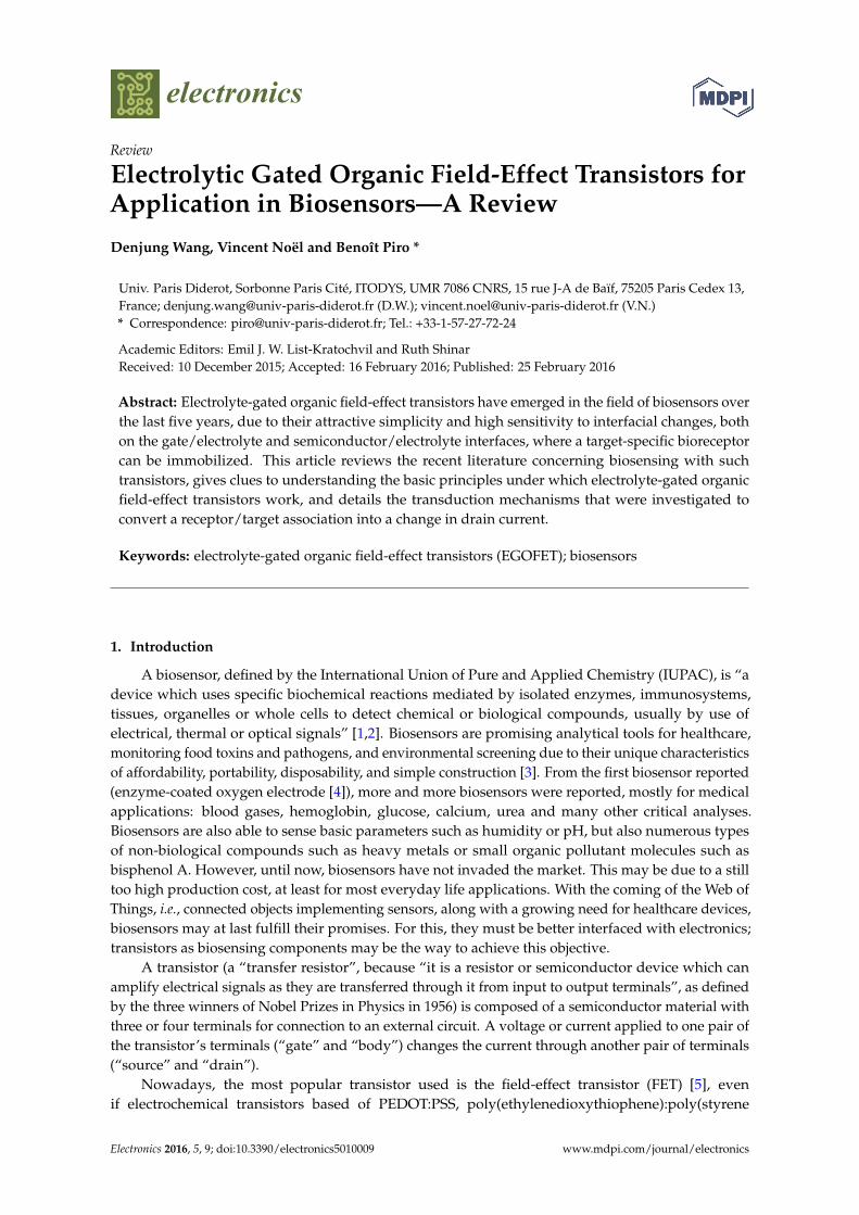
electronics
Review
Electrolytic Gated Organic Field-Effect Transistors forApplication in Biosensors—A Review
Denjung Wang, Vincent Noël and Benoît Piro *
Univ. Paris Diderot, Sorbonne Paris Cité, ITODYS, UMR 7086 CNRS, 15 rue J-A de Baïf, 75205 Paris Cedex 13,France; [email protected] (D.W.); [email protected] (V.N.)* Correspondence: [email protected]; Tel.: +33-1-57-27-72-24
Academic Editors: Emil J. W. List-Kratochvil and Ruth ShinarReceived: 10 December 2015; Accepted: 16 February 2016; Published: 25 February 2016
Abstract: Electrolyte-gated organic field-effect transistors have emerged in the field of biosensors overthe last five years, due to their attractive simplicity and high sensitivity to interfacial changes, bothon the gate/electrolyte and semiconductor/electrolyte interfaces, where a target-specific bioreceptorcan be immobilized. This article reviews the recent literature concerning biosensing with suchtransistors, gives clues to understanding the basic principles under which electrolyte-gated organicfield-effect transistors work, and details the transduction mechanisms that were investigated toconvert a receptor/target association into a change in drain current.
Keywords: electrolyte-gated organic field-effect transistors (EGOFET); biosensors
1. Introduction
A biosensor, defined by the International Union of Pure and Applied Chemistry (IUPAC), is “adevice which uses specific biochemical reactions mediated by isolated enzymes, immunosystems,tissues, organelles or whole cells to detect chemical or biological compounds, usually by use ofelectrical, thermal or optical signals” [1,2]. Biosensors are promising analytical tools for healthcare,monitoring food toxins and pathogens, and environmental screening due to their unique characteristicsof affordability, portability, disposability, and simple construction [3]. From the first biosensor reported(enzyme-coated oxygen electrode [4]), more and more biosensors were reported, mostly for medicalapplications: blood gases, hemoglobin, glucose, calcium, urea and many other critical analyses.Biosensors are also able to sense basic parameters such as humidity or pH, but also numerous typesof non-biological compounds such as heavy metals or small organic pollutant molecules such asbisphenol A. However, until now, biosensors have not invaded the market. This may be due to a stilltoo high production cost, at least for most everyday life applications. With the coming of the Web ofThings, i.e., connected objects implementing sensors, along with a growing need for healthcare devices,biosensors may at last fulfill their promises. For this, they must be better interfaced with electronics;transistors as biosensing components may be the way to achieve this objective.
A transistor (a “transfer resistor”, because “it is a resistor or semiconductor device which canamplify electrical signals as they are transferred through it from input to output terminals”, as definedby the three winners of Nobel Prizes in Physics in 1956) is composed of a semiconductor material withthree or four terminals for connection to an external circuit. A voltage or current applied to one pair ofthe transistor’s terminals (“gate” and “body”) changes the current through another pair of terminals(“source” and “drain”).
Nowadays, the most popular transistor used is the field-effect transistor (FET) [5], evenif electrochemical transistors based of PEDOT:PSS, poly(ethylenedioxythiophene):poly(styrene
Electronics 2016, 5, 9; doi:10.3390/electronics5010009 www.mdpi.com/journal/electronics
Electronics 2016, 5, 9 2 of 24
sulfonate), are widely reported as well [6]. In the past few years, field-effect transistors have beenintensively investigated for biosensing applications, because of their natural integration into portableelectronic devices, but also because the field effect is capacitance-related, and this capacitance is knownto be very sensitive to surface changes. For example, the presence of guest molecules over one of thegate/dielectric or dielectric/semiconductor interface would result in a shift of the conductance of thesemiconductor. However, the main drawback with conventional silicon-based transistors is the highcost of silicon microlithography operated in clean room, which is prohibitive for disposable sensors.Nevertheless, their sensitivities are high, characterized by subthreshold swings of ca. 70 mV/dec forconventional inorganic MOSFETs and significantly lower values for non-conventional FETs such astunneling FETs (10–20 mV/dec), which are based on band-to band tunneling due to band bendinginduced by charges immobilized at the interface between a semiconductor nanowire and a solution [7]).Organic thin-film transistors (OTFTs) will probably never compete with inorganic ones in terms ofcarrier mobility and operating frequency, and their subthreshold swing is often much higher, whichmakes them intrinsically less sensitive up to now. However, organic semiconductors can be processedat low cost, for example by use of printing techniques, and can be easily chemically modified toadjust their properties, which is decisive for biosensors where the recognition elements have to beattached [8].
2. General Concepts of Transistors
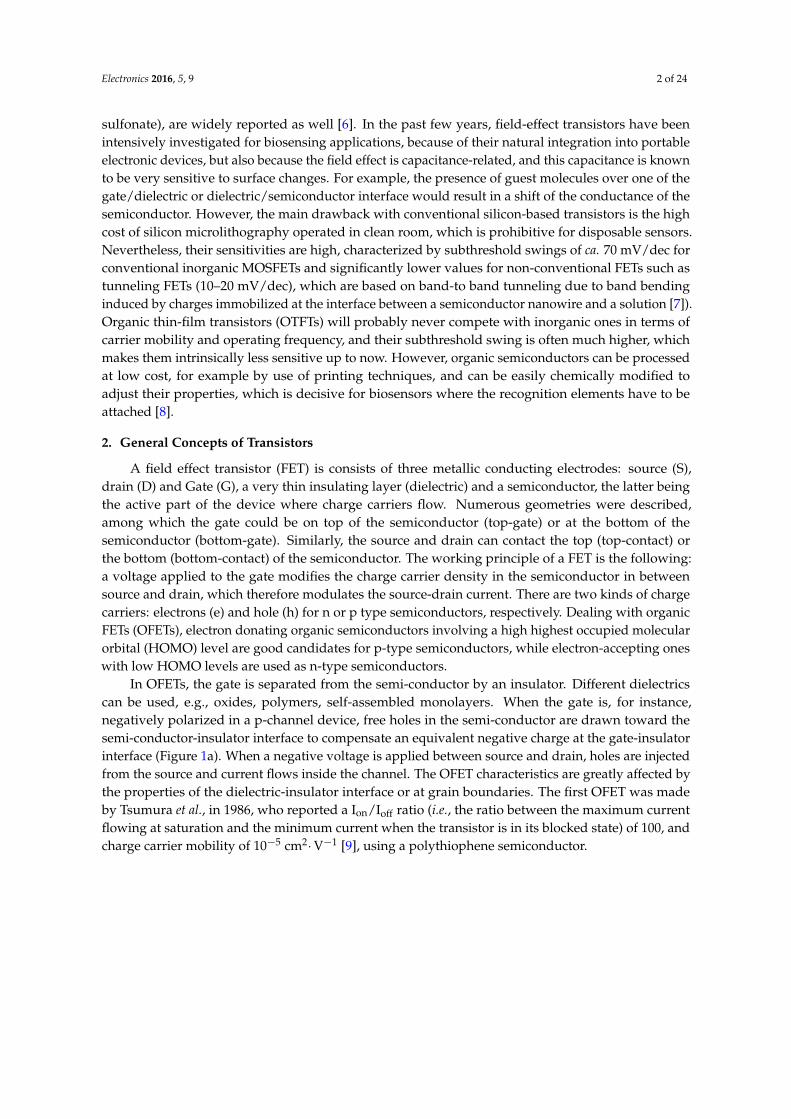
A field effect transistor (FET) is consists of three metallic conducting electrodes: source (S),drain (D) and Gate (G), a very thin insulating layer (dielectric) and a semiconductor, the latter beingthe active part of the device where charge carriers flow. Numerous geometries were described,among which the gate could be on top of the semiconductor (top-gate) or at the bottom of thesemiconductor (bottom-gate). Similarly, the source and drain can contact the top (top-contact) orthe bottom (bottom-contact) of the semiconductor. The working principle of a FET is the following:a voltage applied to the gate modifies the charge carrier density in the semiconductor in betweensource and drain, which therefore modulates the source-drain current. There are two kinds of chargecarriers: electrons (e) and hole (h) for n or p type semiconductors, respectively. Dealing with organicFETs (OFETs), electron donating organic semiconductors involving a high highest occupied molecularorbital (HOMO) level are good candidates for p-type semiconductors, while electron-accepting oneswith low HOMO levels are used as n-type semiconductors.
In OFETs, the gate is separated from the semi-conductor by an insulator. Different dielectricscan be used, e.g., oxides, polymers, self-assembled monolayers. When the gate is, for instance,negatively polarized in a p-channel device, free holes in the semi-conductor are drawn toward thesemi-conductor-insulator interface to compensate an equivalent negative charge at the gate-insulatorinterface (Figure 1a). When a negative voltage is applied between source and drain, holes are injectedfrom the source and current flows inside the channel. The OFET characteristics are greatly affected bythe properties of the dielectric-insulator interface or at grain boundaries. The first OFET was madeby Tsumura et al., in 1986, who reported a Ion/Ioff ratio (i.e., the ratio between the maximum currentflowing at saturation and the minimum current when the transistor is in its blocked state) of 100, andcharge carrier mobility of 10´5 cm2¨ V´1 [9], using a polythiophene semiconductor.
Electronics 2016, 5, 9 3 of 24
Electronics 2016, 5, 9 2 of 23
investigated for biosensing applications, because of their natural integration into portable electronic devices, but also because the field effect is capacitance-related, and this capacitance is known to be very sensitive to surface changes. For example, the presence of guest molecules over one of the gate/dielectric or dielectric/semiconductor interface would result in a shift of the conductance of the semiconductor. However, the main drawback with conventional silicon-based transistors is the high cost of silicon microlithography operated in clean room, which is prohibitive for disposable sensors. Nevertheless, their sensitivities are high, characterized by subthreshold swings of ca. 70 mV/dec for conventional inorganic MOSFETs and significantly lower values for non-conventional FETs such as tunneling FETs (10–20 mV/dec), which are based on band-to band tunneling due to band bending induced by charges immobilized at the interface between a semiconductor nanowire and a solution [7]). Organic thin-film transistors (OTFTs) will probably never compete with inorganic ones in terms of carrier mobility and operating frequency, and their subthreshold swing is often much higher, which makes them intrinsically less sensitive up to now. However, organic semiconductors can be processed at low cost, for example by use of printing techniques, and can be easily chemically modified to adjust their properties, which is decisive for biosensors where the recognition elements have to be attached [8].
2. General Concepts of Transistors
A field effect transistor (FET) is consists of three metallic conducting electrodes: source (S), drain (D) and Gate (G), a very thin insulating layer (dielectric) and a semiconductor, the latter being the active part of the device where charge carriers flow. Numerous geometries were described, among which the gate could be on top of the semiconductor (top-gate) or at the bottom of the semiconductor (bottom-gate). Similarly, the source and drain can contact the top (top-contact) or the bottom (bottom-contact) of the semiconductor. The working principle of a FET is the following: a voltage applied to the gate modifies the charge carrier density in the semiconductor in between source and drain, which therefore modulates the source-drain current. There are two kinds of charge carriers: electrons (e) and hole (h) for n or p type semiconductors, respectively. Dealing with organic FETs (OFETs), electron donating organic semiconductors involving a high highest occupied molecular orbital (HOMO) level are good candidates for p-type semiconductors, while electron-accepting ones with low HOMO levels are used as n-type semiconductors.
In OFETs, the gate is separated from the semi-conductor by an insulator. Different dielectrics can be used, e.g., oxides, polymers, self-assembled monolayers. When the gate is, for instance, negatively polarized in a p-channel device, free holes in the semi-conductor are drawn toward the semi-conductor-insulator interface to compensate an equivalent negative charge at the gate-insulator interface (Figure 1a). When a negative voltage is applied between source and drain, holes are injected from the source and current flows inside the channel. The OFET characteristics are greatly affected by the properties of the dielectric-insulator interface or at grain boundaries. The first OFET was made by Tsumura et al., in 1986, who reported a Ion/Ioff ratio (i.e., the ratio between the maximum current flowing at saturation and the minimum current when the transistor is in its blocked state) of 100, and charge carrier mobility of 10−5 cm2·V−1 [9], using a polythiophene semiconductor.
Figure 1. General scheme of an organic field-effect transistor (OFET) (a) and an electrolyte-gatedorganic field-effect transistor (EGOFET) (b). Adapted from [8] with kind permission from SpringerScience+Business Media. © Springer-Verlag, 2011.
3. EGOFETs
Electrolyte-gated OFETs are significantly different from classical OFETs; indeed, the organicsemiconducting layer is in contact with an electrolyte instead of a classical dielectric. In EGOFETs,the conductivity of the semiconducting channel is modulated by a solid or a liquid electrolyte put inbetween the semiconductor and the gate. EGOFETs display much a higher gate capacitance (up to~1000 higher) than other types of OFETs, which use traditional inorganic or organic non-electrolyticdielectrics; as a consequence, biasing voltages used for EGOFETs are typically much smaller than thosenecessary for OFETs (<1 V, versus >10 V or even higher). These two characteristics (electrolyte—possiblywater—and low potential) make EGOFETs ideal candidates for the next generation of biosensors,particularly suitable for the detection and quantification of biological molecules inside aqueousmedia. The extremely good sensing capabilities of EGOFETs rely on the possibility of properlyfunctionalizing the gate electrode by means of specific molecules or functional groups able to interactwith the target molecules present inside the electrolyte. The most common architecture is the top-gate,bottom-contact configuration. The gate electrode is immersed in the electrolyte and source anddrain electrodes, isolated from the electrolyte, provide electrical contact to the channel (Figure 1b).Actually, an EGOFET looks like an OECT (organic electrochemical transistor) [10–16]. However, in anOECT, the on/off switch is produced by electron transfer from the electrolyte and the semiconductor(doping/de-doping) [8], whereas only capacitive processes occur for EGOFETs but no charge transfer.
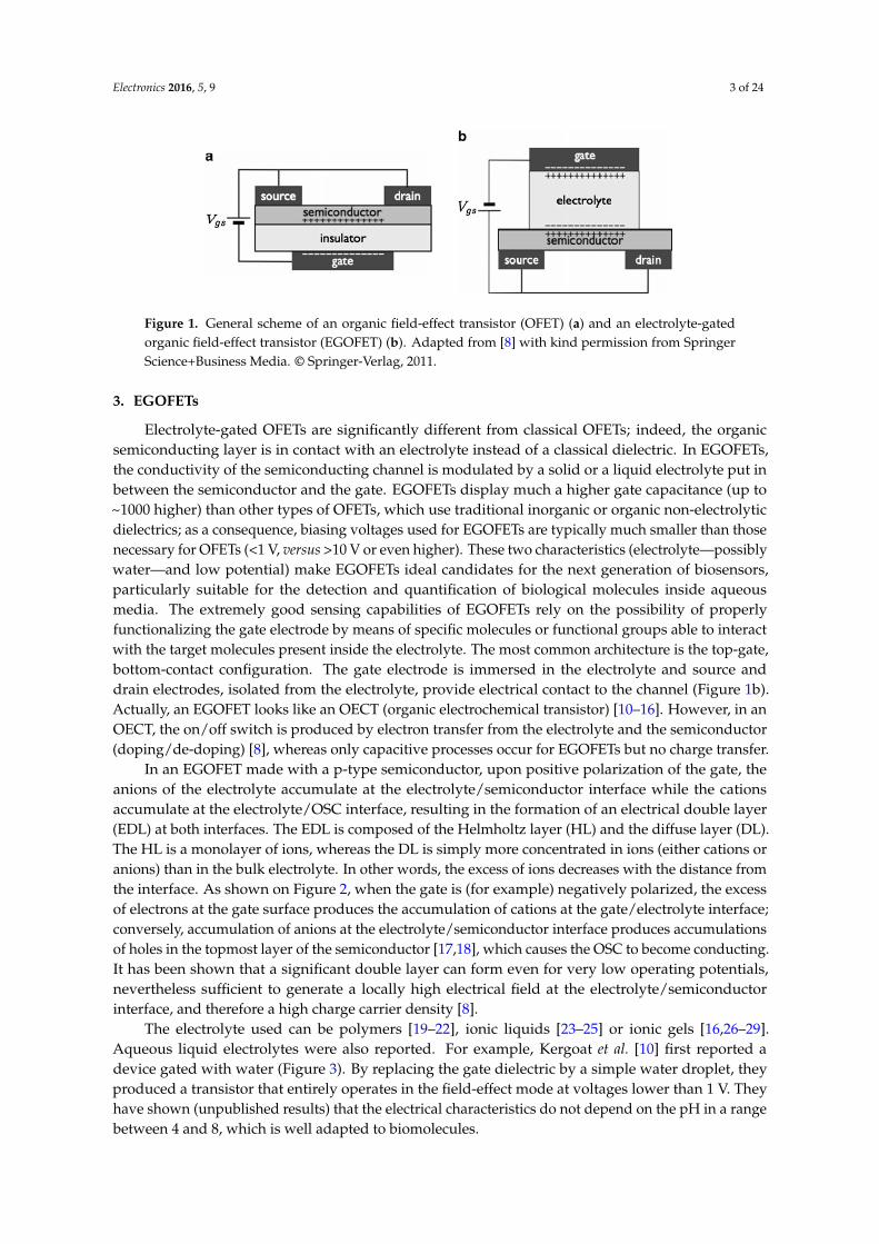
In an EGOFET made with a p-type semiconductor, upon positive polarization of the gate, theanions of the electrolyte accumulate at the electrolyte/semiconductor interface while the cationsaccumulate at the electrolyte/OSC interface, resulting in the formation of an electrical double layer(EDL) at both interfaces. The EDL is composed of the Helmholtz layer (HL) and the diffuse layer (DL).The HL is a monolayer of ions, whereas the DL is simply more concentrated in ions (either cations oranions) than in the bulk electrolyte. In other words, the excess of ions decreases with the distance fromthe interface. As shown on Figure 2, when the gate is (for example) negatively polarized, the excessof electrons at the gate surface produces the accumulation of cations at the gate/electrolyte interface;conversely, accumulation of anions at the electrolyte/semiconductor interface produces accumulationsof holes in the topmost layer of the semiconductor [17,18], which causes the OSC to become conducting.It has been shown that a significant double layer can form even for very low operating potentials,nevertheless sufficient to generate a locally high electrical field at the electrolyte/semiconductorinterface, and therefore a high charge carrier density [8].
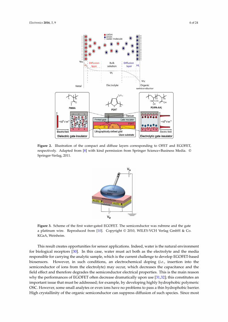
The electrolyte used can be polymers [19–22], ionic liquids [23–25] or ionic gels [16,26–29].Aqueous liquid electrolytes were also reported. For example, Kergoat et al. [10] first reported adevice gated with water (Figure 3). By replacing the gate dielectric by a simple water droplet, theyproduced a transistor that entirely operates in the field-effect mode at voltages lower than 1 V. Theyhave shown (unpublished results) that the electrical characteristics do not depend on the pH in a rangebetween 4 and 8, which is well adapted to biomolecules.
Electronics 2016, 5, 9 4 of 24
Electronics 2016, 5, 9 3 of 23
Figure 1. General scheme of an organic field-effect transistor (OFET) (a) and an electrolyte-gated organic field-effect transistor (EGOFET) (b). Adapted from [8] with kind permission from Springer Science+Business Media. © Springer-Verlag, 2011.
3. EGOFETs
Electrolyte-gated OFETs are significantly different from classical OFETs; indeed, the organic semiconducting layer is in contact with an electrolyte instead of a classical dielectric. In EGOFETs, the conductivity of the semiconducting channel is modulated by a solid or a liquid electrolyte put in between the semiconductor and the gate. EGOFETs display much a higher gate capacitance (up to ~1000 higher) than other types of OFETs, which use traditional inorganic or organic non-electrolytic dielectrics; as a consequence, biasing voltages used for EGOFETs are typically much smaller than those necessary for OFETs (<1 V, versus >10 V or even higher). These two characteristics (electrolyte—possibly water—and low potential) make EGOFETs ideal candidates for the next generation of biosensors, particularly suitable for the detection and quantification of biological molecules inside aqueous media. The extremely good sensing capabilities of EGOFETs rely on the possibility of properly functionalizing the gate electrode by means of specific molecules or functional groups able to interact with the target molecules present inside the electrolyte. The most common architecture is the top-gate, bottom-contact configuration. The gate electrode is immersed in the electrolyte and source and drain electrodes, isolated from the electrolyte, provide electrical contact to the channel (Figure 1b). Actually, an EGOFET looks like an OECT (organic electrochemical transistor) [10–16]. However, in an OECT, the on/off switch is produced by electron transfer from the electrolyte and the semiconductor (doping/de-doping) [8], whereas only capacitive processes occur for EGOFETs but no charge transfer.
In an EGOFET made with a p-type semiconductor, upon positive polarization of the gate, the anions of the electrolyte accumulate at the electrolyte/semiconductor interface while the cations accumulate at the electrolyte/OSC interface, resulting in the formation of an electrical double layer (EDL) at both interfaces. The EDL is composed of the Helmholtz layer (HL) and the diffuse layer (DL). The HL is a monolayer of ions, whereas the DL is simply more concentrated in ions (either cations or anions) than in the bulk electrolyte. In other words, the excess of ions decreases with the distance from the interface. As shown on Figure 2, when the gate is (for example) negatively polarized, the excess of electrons at the gate surface produces the accumulation of cations at the gate/electrolyte interface; conversely, accumulation of anions at the electrolyte/semiconductor interface produces accumulations of holes in the topmost layer of the semiconductor [17,18], which causes the OSC to become conducting. It has been shown that a significant double layer can form even for very low operating potentials, nevertheless sufficient to generate a locally high electrical field at the electrolyte/semiconductor interface, and therefore a high charge carrier density [8].
Electronics 2016, 5, 9 4 of 23
Figure 2. Illustration of the compact and diffuse layers corresponding to OFET and EGOFET, respectively. Adapted from [8] with kind permission from Springer Science+Business Media. © Springer-Verlag, 2011.
The electrolyte used can be polymers [19–22], ionic liquids [23–25] or ionic gels [16,26–29]. Aqueous liquid electrolytes were also reported. For example, Kergoat et al. [10] first reported a device gated with water (Figure 3). By replacing the gate dielectric by a simple water droplet, they produced a transistor that entirely operates in the field-effect mode at voltages lower than 1 V. They have shown (unpublished results) that the electrical characteristics do not depend on the pH in a range between 4 and 8, which is well adapted to biomolecules.
Figure 3. Scheme of the first water-gated EGOFET. The semiconductor was rubrene and the gate a platinum wire. Reproduced from [10]. Copyright © 2010, WILEY-VCH Verlag GmbH & Co. KGaA, Weinheim.
This result creates opportunities for sensor applications. Indeed, water is the natural environment for biological receptors [30]. In this case, water must act both as the electrolyte and the media responsible for carrying the analytic sample, which is the current challenge to develop EGOFET-based biosensors. However, in such conditions, an electrochemical doping (i.e., insertion into the semiconductor of ions from the electrolyte) may occur, which decreases the capacitance and the field effect and therefore degrades the semiconductor electrical properties. This is the main reason why the performances of EGOFET often decrease dramatically upon use [31,32]; this constitutes an important issue that must be addressed; for example, by developing highly hydrophobic polymeric OSC. However, some small analytes or even ions have no problems to pass a thin hydrophobic barrier. High crystallinity of the organic semiconductor can suppress diffusion of such species. Since most polymer films are semi-crystalline at best, this might be an aspect where crystalline films made from small molecules might be superior in terms of blocking and should be investigated. Another issue that must be addressed is their high subthreshold swing, typically of several hundreds of millivolts, which impede their sensitivity. A strategy may be to switch from
Figure 2. Illustration of the compact and diffuse layers corresponding to OFET and EGOFET,respectively. Adapted from [8] with kind permission from Springer Science+Business Media. ©Springer-Verlag, 2011.
Electronics 2016, 5, 9 4 of 23
Figure 2. Illustration of the compact and diffuse layers corresponding to OFET and EGOFET, respectively. Adapted from [8] with kind permission from Springer Science+Business Media. © Springer-Verlag, 2011.
The electrolyte used can be polymers [19–22], ionic liquids [23–25] or ionic gels [16,26–29]. Aqueous liquid electrolytes were also reported. For example, Kergoat et al. [10] first reported a device gated with water (Figure 3). By replacing the gate dielectric by a simple water droplet, they produced a transistor that entirely operates in the field-effect mode at voltages lower than 1 V. They have shown (unpublished results) that the electrical characteristics do not depend on the pH in a range between 4 and 8, which is well adapted to biomolecules.
Figure 3. Scheme of the first water-gated EGOFET. The semiconductor was rubrene and the gate a platinum wire. Reproduced from [10]. Copyright © 2010, WILEY-VCH Verlag GmbH & Co. KGaA, Weinheim.
This result creates opportunities for sensor applications. Indeed, water is the natural environment for biological receptors [30]. In this case, water must act both as the electrolyte and the media responsible for carrying the analytic sample, which is the current challenge to develop EGOFET-based biosensors. However, in such conditions, an electrochemical doping (i.e., insertion into the semiconductor of ions from the electrolyte) may occur, which decreases the capacitance and the field effect and therefore degrades the semiconductor electrical properties. This is the main reason why the performances of EGOFET often decrease dramatically upon use [31,32]; this constitutes an important issue that must be addressed; for example, by developing highly hydrophobic polymeric OSC. However, some small analytes or even ions have no problems to pass a thin hydrophobic barrier. High crystallinity of the organic semiconductor can suppress diffusion of such species. Since most polymer films are semi-crystalline at best, this might be an aspect where crystalline films made from small molecules might be superior in terms of blocking and should be investigated. Another issue that must be addressed is their high subthreshold swing, typically of several hundreds of millivolts, which impede their sensitivity. A strategy may be to switch from
Figure 3. Scheme of the first water-gated EGOFET. The semiconductor was rubrene and the gatea platinum wire. Reproduced from [10]. Copyright © 2010, WILEY-VCH Verlag GmbH & Co.KGaA, Weinheim.
This result creates opportunities for sensor applications. Indeed, water is the natural environmentfor biological receptors [30]. In this case, water must act both as the electrolyte and the mediaresponsible for carrying the analytic sample, which is the current challenge to develop EGOFET-basedbiosensors. However, in such conditions, an electrochemical doping (i.e., insertion into thesemiconductor of ions from the electrolyte) may occur, which decreases the capacitance and thefield effect and therefore degrades the semiconductor electrical properties. This is the main reasonwhy the performances of EGOFET often decrease dramatically upon use [31,32]; this constitutes animportant issue that must be addressed; for example, by developing highly hydrophobic polymericOSC. However, some small analytes or even ions have no problems to pass a thin hydrophobic barrier.High crystallinity of the organic semiconductor can suppress diffusion of such species. Since most
Electronics 2016, 5, 9 5 of 24
polymer films are semi-crystalline at best, this might be an aspect where crystalline films made fromsmall molecules might be superior in terms of blocking and should be investigated. Another issue thatmust be addressed is their high subthreshold swing, typically of several hundreds of millivolts, whichimpede their sensitivity. A strategy may be to switch from classical OSC to graphene-based materials,e.g., graphene or reduced graphene oxide, which has already been reported [33–46], but this will notbe discussed here. Readers who are interested in grapheme-based EGOFETs may report on the reviewfrom Yan et al., 2013, which dealt with graphene-based transistors for biological sensors [47]. However,graphene has been shown to have low sensitivity due to lack of bandgap. For this reason, otherelectrolyte-gated inorganic FETs are also promising, for example based on MoS2 semiconductor [48]. InEGOFETs, the gate material also influences the figures of merit of the devices, particularly the thresholdpotential VT [49,50]. However, most of the transistor characteristics come from the semiconductingmaterial itself and from the quality of the contact between the source and drain electrodes and theOSC. This quality noticeably depends on the way the semiconductor is deposited.
4. Semiconducting Materials
4.1. Deposition Techniques
Several deposition techniques were described; among them: spin coating, vacuum thermaldeposition, printing and spray deposition. Spin-coating and drop-casting remain the most popular inlaboratory, whereas inkjet printing and spray deposition are preferentially used in industry; vacuumthermal evaporation is used in both environments.
4.1.1. Vacuum Thermal Evaporation
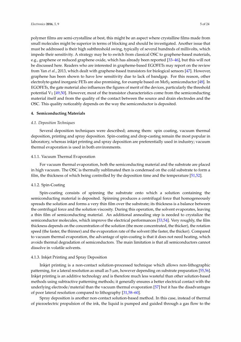
For vacuum thermal evaporation, both the semiconducting material and the substrate are placedin high vacuum. The OSC is thermally sublimated then is condensed on the cold substrate to form afilm, the thickness of which being controlled by the deposition time and the temperature [51,52].
4.1.2. Spin-Coating
Spin-coating consists of spinning the substrate onto which a solution containing thesemiconducting material is deposited. Spinning produces a centrifugal force that homogeneouslyspreads the solution and forms a very thin film over the substrate; its thickness is a balance betweenthe centrifugal force and the solution viscosity. During this operation, the solvent evaporates, leavinga thin film of semiconducting material. An additional annealing step is needed to crystalize thesemiconductor molecules, which improve the electrical performances [53,54]. Very roughly, the filmthickness depends on the concentration of the solution (the more concentrated, the thicker), the rotationspeed (the faster, the thinner) and the evaporation rate of the solvent (the faster, the thicker). Comparedto vacuum thermal evaporation, the advantage of spin-coating is that it does not need heating, whichavoids thermal degradation of semiconductors. The main limitation is that all semiconductors cannotdissolve in volatile solvents.
4.1.3. Inkjet Printing and Spray Deposition
Inkjet printing is a non-contact solution-processed technique which allows non-lithographicpatterning, for a lateral resolution as small as 5 µm, however depending on substrate preparation [55,56].Inkjet printing is an additive technology and is therefore much less wasteful than other solution-basedmethods using subtractive patterning methods; it generally ensures a better electrical contact with theunderlying electrode/material than the vacuum thermal evaporation [57] but it has the disadvantagesof poor lateral resolution compared to lithography [31,58–60].
Spray deposition is another non-contact solution-based method. In this case, instead of thermalof piezoelectric propulsion of the ink, the liquid is pumped and guided through a gas flow to the
Electronics 2016, 5, 9 6 of 24
substrate. Like for inkjet-printing, the ink arrives at the substrate as micrometric droplets. For thisreason, a challenge for both techniques is to achieve uniform films [52,61].
4.2. Semiconducting Materials
4.2.1. Generalities
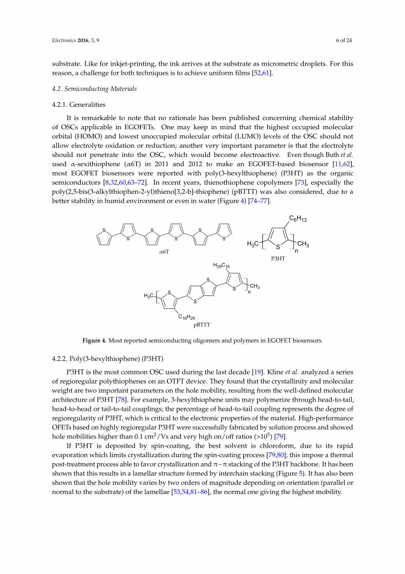
It is remarkable to note that no rationale has been published concerning chemical stabilityof OSCs applicable in EGOFETs. One may keep in mind that the highest occupied molecularorbital (HOMO) and lowest unoccupied molecular orbital (LUMO) levels of the OSC should notallow electrolyte oxidation or reduction; another very important parameter is that the electrolyteshould not penetrate into the OSC, which would become electroactive. Even though Buth et al.used α-sexithiophene (α6T) in 2011 and 2012 to make an EGOFET-based biosensor [11,62],most EGOFET biosensors were reported with poly(3-hexylthiophene) (P3HT) as the organicsemiconductors [8,32,60,63–72]. In recent years, thienothiophene copolymers [73], especially thepoly(2,5-bis(3-alkylthiophen-2-yl)thieno[3,2-b]-thiophene) (pBTTT) was also considered, due to abetter stability in humid environment or even in water (Figure 4) [74–77].
Electronics 2016, 5, 9 6 of 23
4.2. Semiconducting Materials
4.2.1. Generalities
It is remarkable to note that no rationale has been published concerning chemical stability of OSCs applicable in EGOFETs. One may keep in mind that the highest occupied molecular orbital (HOMO) and lowest unoccupied molecular orbital (LUMO) levels of the OSC should not allow electrolyte oxidation or reduction; another very important parameter is that the electrolyte should not penetrate into the OSC, which would become electroactive. Even though Buth et al. used α-sexithiophene (α6T) in 2011 and 2012 to make an EGOFET-based biosensor [11,62], most EGOFET biosensors were reported with poly(3-hexylthiophene) (P3HT) as the organic semiconductors [8,32,60,63–72]. In recent years, thienothiophene copolymers [73], especially the poly(2,5-bis(3-alkylthiophen-2-yl)thieno[3,2-b]-thiophene) (pBTTT) was also considered, due to a better stability in humid environment or even in water (Figure 4) [74–77].
α6T
P3HT
pBTTT
Figure 4. Most reported semiconducting oligomers and polymers in EGOFET biosensors.
4.2.2. Poly(3-hexylthiophene) (P3HT)
P3HT is the most common OSC used during the last decade [19]. Kline et al. analyzed a series of regioregular polythiophenes on an OTFT device. They found that the crystallinity and molecular weight are two important parameters on the hole mobility, resulting from the well-defined molecular architecture of P3HT [78]. For example, 3-hexylthiophene units may polymerize through head-to-tail, head-to-head or tail-to-tail couplings; the percentage of head-to-tail coupling represents the degree of regioregularity of P3HT, which is critical to the electronic properties of the material. High-performance OFETs based on highly regioregular P3HT were successfully fabricated by solution process and showed hole mobilities higher than 0.1 cm2/Vs and very high on/off ratios (>105) [79].
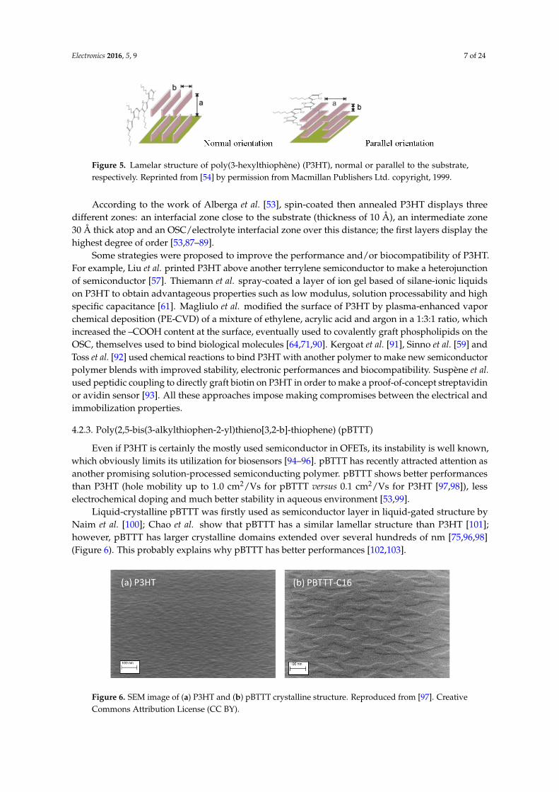
If P3HT is deposited by spin-coating, the best solvent is chloroform, due to its rapid evaporation which limits crystallization during the spin-coating process [79,80]; this impose a thermal post-treatment process able to favor crystallization and π−π stacking of the P3HT backbone. It has been shown that this results in a lamellar structure formed by interchain stacking (Figure 5). It has also been shown that the hole mobility varies by two orders of magnitude depending on orientation (parallel or normal to the substrate) of the lamellae [53,54,81–86], the normal one giving the highest mobility.
S
S S
SS
S
CH3SCH3
C6H13
n
S
S
S
SCH3
CH3
H29C16
C16H29
n
Figure 4. Most reported semiconducting oligomers and polymers in EGOFET biosensors.
4.2.2. Poly(3-hexylthiophene) (P3HT)
P3HT is the most common OSC used during the last decade [19]. Kline et al. analyzed a seriesof regioregular polythiophenes on an OTFT device. They found that the crystallinity and molecularweight are two important parameters on the hole mobility, resulting from the well-defined moleculararchitecture of P3HT [78]. For example, 3-hexylthiophene units may polymerize through head-to-tail,head-to-head or tail-to-tail couplings; the percentage of head-to-tail coupling represents the degree ofregioregularity of P3HT, which is critical to the electronic properties of the material. High-performanceOFETs based on highly regioregular P3HT were successfully fabricated by solution process and showedhole mobilities higher than 0.1 cm2/Vs and very high on/off ratios (>105) [79].
If P3HT is deposited by spin-coating, the best solvent is chloroform, due to its rapidevaporation which limits crystallization during the spin-coating process [79,80]; this impose a thermalpost-treatment process able to favor crystallization and π´π stacking of the P3HT backbone. It has beenshown that this results in a lamellar structure formed by interchain stacking (Figure 5). It has also beenshown that the hole mobility varies by two orders of magnitude depending on orientation (parallel ornormal to the substrate) of the lamellae [53,54,81–86], the normal one giving the highest mobility.
Electronics 2016, 5, 9 7 of 24
Electronics 2016, 5, 9 7 of 23
Figure 5. Lamelar structure of poly(3-hexylthiophène) (P3HT), normal or parallel to the substrate, respectively. Reprinted from [54] by permission from Macmillan Publishers Ltd. copyright, 1999.
According to the work of Alberga et al. [53], spin-coated then annealed P3HT displays three different zones: an interfacial zone close to the substrate (thickness of 10 Å), an intermediate zone 30 Å thick atop and an OSC/electrolyte interfacial zone over this distance; the first layers display the highest degree of order [53,87–89].
Some strategies were proposed to improve the performance and/or biocompatibility of P3HT. For example, Liu et al. printed P3HT above another terrylene semiconductor to make a heterojunction of semiconductor [57]. Thiemann et al. spray-coated a layer of ion gel based of silane-ionic liquids on P3HT to obtain advantageous properties such as low modulus, solution processability and high specific capacitance [61]. Magliulo et al. modified the surface of P3HT by plasma-enhanced vapor chemical deposition (PE-CVD) of a mixture of ethylene, acrylic acid and argon in a 1:3:1 ratio, which increased the –COOH content at the surface, eventually used to covalently graft phospholipids on the OSC, themselves used to bind biological molecules [64,71,90]. Kergoat et al. [91], Sinno et al. [59] and Toss et al. [92] used chemical reactions to bind P3HT with another polymer to make new semiconductor polymer blends with improved stability, electronic performances and biocompatibility. Suspène et al. used peptidic coupling to directly graft biotin on P3HT in order to make a proof-of-concept streptavidin or avidin sensor [93]. All these approaches impose making compromises between the electrical and immobilization properties.
4.2.3. Poly(2,5-bis(3-alkylthiophen-2-yl)thieno[3,2-b]-thiophene) (pBTTT)
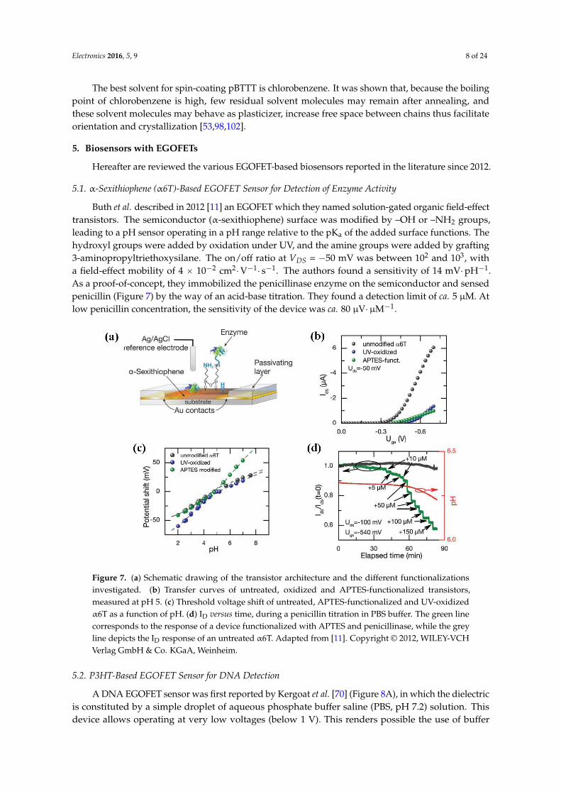
Even if P3HT is certainly the mostly used semiconductor in OFETs, its instability is well known, which obviously limits its utilization for biosensors [94–96]. pBTTT has recently attracted attention as another promising solution-processed semiconducting polymer. pBTTT shows better performances than P3HT (hole mobility up to 1.0 cm2/Vs for pBTTT versus 0.1 cm2/Vs for P3HT [97,98]), less electrochemical doping and much better stability in aqueous environment [53,99].
Liquid-crystalline pBTTT was firstly used as semiconductor layer in liquid-gated structure by Naim et al. [100]; Chao et al. show that pBTTT has a similar lamellar structure than P3HT [101]; however, pBTTT has larger crystalline domains extended over several hundreds of nm [75,96,98] (Figure 6). This probably explains why pBTTT has better performances [102,103].
Figure 6. SEM image of (a) P3HT and (b) pBTTT crystalline structure. Reproduced from [97]. Creative Commons Attribution License (CC BY).
Figure 5. Lamelar structure of poly(3-hexylthiophène) (P3HT), normal or parallel to the substrate,respectively. Reprinted from [54] by permission from Macmillan Publishers Ltd. copyright, 1999.
According to the work of Alberga et al. [53], spin-coated then annealed P3HT displays threedifferent zones: an interfacial zone close to the substrate (thickness of 10 Å), an intermediate zone30 Å thick atop and an OSC/electrolyte interfacial zone over this distance; the first layers display thehighest degree of order [53,87–89].
Some strategies were proposed to improve the performance and/or biocompatibility of P3HT.For example, Liu et al. printed P3HT above another terrylene semiconductor to make a heterojunctionof semiconductor [57]. Thiemann et al. spray-coated a layer of ion gel based of silane-ionic liquidson P3HT to obtain advantageous properties such as low modulus, solution processability and highspecific capacitance [61]. Magliulo et al. modified the surface of P3HT by plasma-enhanced vaporchemical deposition (PE-CVD) of a mixture of ethylene, acrylic acid and argon in a 1:3:1 ratio, whichincreased the –COOH content at the surface, eventually used to covalently graft phospholipids on theOSC, themselves used to bind biological molecules [64,71,90]. Kergoat et al. [91], Sinno et al. [59] andToss et al. [92] used chemical reactions to bind P3HT with another polymer to make new semiconductorpolymer blends with improved stability, electronic performances and biocompatibility. Suspène et al.used peptidic coupling to directly graft biotin on P3HT in order to make a proof-of-concept streptavidinor avidin sensor [93]. All these approaches impose making compromises between the electrical andimmobilization properties.
4.2.3. Poly(2,5-bis(3-alkylthiophen-2-yl)thieno[3,2-b]-thiophene) (pBTTT)
Even if P3HT is certainly the mostly used semiconductor in OFETs, its instability is well known,which obviously limits its utilization for biosensors [94–96]. pBTTT has recently attracted attention asanother promising solution-processed semiconducting polymer. pBTTT shows better performancesthan P3HT (hole mobility up to 1.0 cm2/Vs for pBTTT versus 0.1 cm2/Vs for P3HT [97,98]), lesselectrochemical doping and much better stability in aqueous environment [53,99].
Liquid-crystalline pBTTT was firstly used as semiconductor layer in liquid-gated structure byNaim et al. [100]; Chao et al. show that pBTTT has a similar lamellar structure than P3HT [101];however, pBTTT has larger crystalline domains extended over several hundreds of nm [75,96,98](Figure 6). This probably explains why pBTTT has better performances [102,103].
Electronics 2016, 5, 9 7 of 23
Figure 5. Lamelar structure of poly(3-hexylthiophène) (P3HT), normal or parallel to the substrate, respectively. Reprinted from [54] by permission from Macmillan Publishers Ltd. copyright, 1999.
According to the work of Alberga et al. [53], spin-coated then annealed P3HT displays three different zones: an interfacial zone close to the substrate (thickness of 10 Å), an intermediate zone 30 Å thick atop and an OSC/electrolyte interfacial zone over this distance; the first layers display the highest degree of order [53,87–89].
Some strategies were proposed to improve the performance and/or biocompatibility of P3HT. For example, Liu et al. printed P3HT above another terrylene semiconductor to make a heterojunction of semiconductor [57]. Thiemann et al. spray-coated a layer of ion gel based of silane-ionic liquids on P3HT to obtain advantageous properties such as low modulus, solution processability and high specific capacitance [61]. Magliulo et al. modified the surface of P3HT by plasma-enhanced vapor chemical deposition (PE-CVD) of a mixture of ethylene, acrylic acid and argon in a 1:3:1 ratio, which increased the –COOH content at the surface, eventually used to covalently graft phospholipids on the OSC, themselves used to bind biological molecules [64,71,90]. Kergoat et al. [91], Sinno et al. [59] and Toss et al. [92] used chemical reactions to bind P3HT with another polymer to make new semiconductor polymer blends with improved stability, electronic performances and biocompatibility. Suspène et al. used peptidic coupling to directly graft biotin on P3HT in order to make a proof-of-concept streptavidin or avidin sensor [93]. All these approaches impose making compromises between the electrical and immobilization properties.
4.2.3. Poly(2,5-bis(3-alkylthiophen-2-yl)thieno[3,2-b]-thiophene) (pBTTT)
Even if P3HT is certainly the mostly used semiconductor in OFETs, its instability is well known, which obviously limits its utilization for biosensors [94–96]. pBTTT has recently attracted attention as another promising solution-processed semiconducting polymer. pBTTT shows better performances than P3HT (hole mobility up to 1.0 cm2/Vs for pBTTT versus 0.1 cm2/Vs for P3HT [97,98]), less electrochemical doping and much better stability in aqueous environment [53,99].
Liquid-crystalline pBTTT was firstly used as semiconductor layer in liquid-gated structure by Naim et al. [100]; Chao et al. show that pBTTT has a similar lamellar structure than P3HT [101]; however, pBTTT has larger crystalline domains extended over several hundreds of nm [75,96,98] (Figure 6). This probably explains why pBTTT has better performances [102,103].
Figure 6. SEM image of (a) P3HT and (b) pBTTT crystalline structure. Reproduced from [97]. Creative Commons Attribution License (CC BY). Figure 6. SEM image of (a) P3HT and (b) pBTTT crystalline structure. Reproduced from [97]. Creative
Commons Attribution License (CC BY).
Electronics 2016, 5, 9 8 of 24
The best solvent for spin-coating pBTTT is chlorobenzene. It was shown that, because the boilingpoint of chlorobenzene is high, few residual solvent molecules may remain after annealing, andthese solvent molecules may behave as plasticizer, increase free space between chains thus facilitateorientation and crystallization [53,98,102].
5. Biosensors with EGOFETs
Hereafter are reviewed the various EGOFET-based biosensors reported in the literature since 2012.
5.1. α-Sexithiophene (α6T)-Based EGOFET Sensor for Detection of Enzyme Activity
Buth et al. described in 2012 [11] an EGOFET which they named solution-gated organic field-effecttransistors. The semiconductor (α-sexithiophene) surface was modified by –OH or –NH2 groups,leading to a pH sensor operating in a pH range relative to the pKa of the added surface functions. Thehydroxyl groups were added by oxidation under UV, and the amine groups were added by grafting3-aminopropyltriethoxysilane. The on/off ratio at VDS = ´50 mV was between 102 and 103, witha field-effect mobility of 4 ˆ 10´2 cm2¨ V´1¨ s´1. The authors found a sensitivity of 14 mV¨ pH´1.As a proof-of-concept, they immobilized the penicillinase enzyme on the semiconductor and sensedpenicillin (Figure 7) by the way of an acid-base titration. They found a detection limit of ca. 5 µM. Atlow penicillin concentration, the sensitivity of the device was ca. 80 µV¨µM´1.
Electronics 2016, 5, 9 8 of 23
The best solvent for spin-coating pBTTT is chlorobenzene. It was shown that, because the boiling point of chlorobenzene is high, few residual solvent molecules may remain after annealing, and these solvent molecules may behave as plasticizer, increase free space between chains thus facilitate orientation and crystallization [53,98,102].
5. Biosensors with EGOFETs
Hereafter are reviewed the various EGOFET-based biosensors reported in the literature since 2012.
5.1. α-Sexithiophene (α6T)-Based EGOFET Sensor for Detection of Enzyme Activity
Buth et al. described in 2012 [11] an EGOFET which they named solution-gated organic field-effect transistors. The semiconductor (α-sexithiophene) surface was modified by –OH or –NH2 groups, leading to a pH sensor operating in a pH range relative to the pKa of the added surface functions. The hydroxyl groups were added by oxidation under UV, and the amine groups were added by grafting 3-aminopropyltriethoxysilane. The on/off ratio at VDS = −50 mV was between 102 and 103, with a field-effect mobility of 4 × 10⁻² cm2·V−1·s−1. The authors found a sensitivity of 14 mV·pH−1. As a proof-of-concept, they immobilized the penicillinase enzyme on the semiconductor and sensed penicillin (Figure 7) by the way of an acid-base titration. They found a detection limit of ca. 5 μM. At low penicillin concentration, the sensitivity of the device was ca. 80 μV·μM−1.
Figure 7. (a) Schematic drawing of the transistor architecture and the different functionalizations investigated. (b) Transfer curves of untreated, oxidized and APTES-functionalized transistors, measured at pH 5. (c) Threshold voltage shift of untreated, APTES-functionalized and UV-oxidized α6T as a function of pH. (d) ID versus time, during a penicillin titration in PBS buffer. The green line corresponds to the response of a device functionalized with APTES and penicillinase, while the grey line depicts the ID response of an untreated α6T. Adapted from [11]. Copyright © 2012, WILEY-VCH Verlag GmbH & Co. KGaA, Weinheim.
5.2. P3HT-Based EGOFET Sensor for DNA Detection
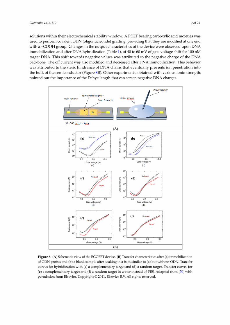
A DNA EGOFET sensor was first reported by Kergoat et al. [70] (Figure 8A), in which the dielectric is constituted by a simple droplet of aqueous phosphate buffer saline (PBS, pH 7.2)
Figure 7. (a) Schematic drawing of the transistor architecture and the different functionalizationsinvestigated. (b) Transfer curves of untreated, oxidized and APTES-functionalized transistors,measured at pH 5. (c) Threshold voltage shift of untreated, APTES-functionalized and UV-oxidizedα6T as a function of pH. (d) ID versus time, during a penicillin titration in PBS buffer. The green linecorresponds to the response of a device functionalized with APTES and penicillinase, while the greyline depicts the ID response of an untreated α6T. Adapted from [11]. Copyright © 2012, WILEY-VCHVerlag GmbH & Co. KGaA, Weinheim.
5.2. P3HT-Based EGOFET Sensor for DNA Detection
A DNA EGOFET sensor was first reported by Kergoat et al. [70] (Figure 8A), in which the dielectricis constituted by a simple droplet of aqueous phosphate buffer saline (PBS, pH 7.2) solution. Thisdevice allows operating at very low voltages (below 1 V). This renders possible the use of buffer
Electronics 2016, 5, 9 9 of 24
solutions within their electrochemical stability window. A P3HT bearing carboxylic acid moieties wasused to perform covalent ODN (oligonucleotide) grafting, providing that they are modified at one endwith a –COOH group. Changes in the output characteristics of the device were observed upon DNAimmobilization and after DNA hybridization (Table 1), of 40 to 60 mV of gate voltage shift for 100 nMtarget DNA. This shift towards negative values was attributed to the negative charge of the DNAbackbone. The off current was also modified and decreased after DNA immobilization. This behaviorwas attributed to the steric hindrance of DNA chains that eventually prevents ion penetration intothe bulk of the semiconductor (Figure 8B). Other experiments, obtained with various ionic strength,pointed out the importance of the Debye length that can screen negative DNA charges.
Electronics 2016, 5, 9 9 of 23
solution. This device allows operating at very low voltages (below 1 V). This renders possible the use of buffer solutions within their electrochemical stability window. A P3HT bearing carboxylic acid moieties was used to perform covalent ODN (oligonucleotide) grafting, providing that they are modified at one end with a –COOH group. Changes in the output characteristics of the device were observed upon DNA immobilization and after DNA hybridization (Table 1), of 40 to 60 mV of gate voltage shift for 100 nM target DNA. This shift towards negative values was attributed to the negative charge of the DNA backbone. The off current was also modified and decreased after DNA immobilization. This behavior was attributed to the steric hindrance of DNA chains that eventually prevents ion penetration into the bulk of the semiconductor (Figure 8B). Other experiments, obtained with various ionic strength, pointed out the importance of the Debye length that can screen negative DNA charges.
(A)
(B)
Figure 8. (A) Schematic view of the EGOFET device. (B) Transfer characteristics after (a) immobilization of ODN probes and (b) a blank sample after soaking in a bath similar to (a) but without ODN. Transfer curves for hybridization with (c) a complementary target and (d) a random target. Transfer curves for (e) a complementary target and (f) a random target in water instead of PBS. Adapted from [70] with permission from Elsevier. Copyright © 2011, Elsevier B.V. All rights reserved.
Figure 8. (A) Schematic view of the EGOFET device. (B) Transfer characteristics after (a) immobilizationof ODN probes and (b) a blank sample after soaking in a bath similar to (a) but without ODN. Transfercurves for hybridization with (c) a complementary target and (d) a random target. Transfer curves for(e) a complementary target and (f) a random target in water instead of PBS. Adapted from [70] withpermission from Elsevier. Copyright © 2011, Elsevier B.V. All rights reserved.
Electronics 2016, 5, 9 10 of 24
Table 1. Influence of probe grafting and target hybridization on device performance with phosphatebuffer saline (PBS) as electrolyte, and influence of probe hybridization with water as electrolyte.Adapted from [70] with permission from Elsevier. Copyright © 2011, Elsevier B.V. All rights reserved.
ODN grafting (Figure 8a,b)
ODN probe ∆VG min / V Ioff (bare film){ Ioff (probe-modified film)Yes ´0.31 ˘ 0.05 11.1 ˘ 3.7No +0.16 ˘ 0.05 0.5 ˘ 0.12
DNA hybrid. in PBS (Figure 8c,d)ODN target ∆VG min / V Ioff (probe-modified film){ Ioff (hybridization)
HIV ´0.06 ˘ 0.02 1.7 ˘ 0.45RAND ´0.03 ˘ 0.03 1.3 ˘ 0.28
DNA hybrid. in H2O (Figure 8e,f)ODN probe ∆VGmin / V Ioff (probe-modified film){ Ioff (hybridization)
HIV ´0.03 ˘ 0.02 3.4 ˘ 1.5RAND ´0.04 ˘ 0.07 1.04 ˘ 0.04
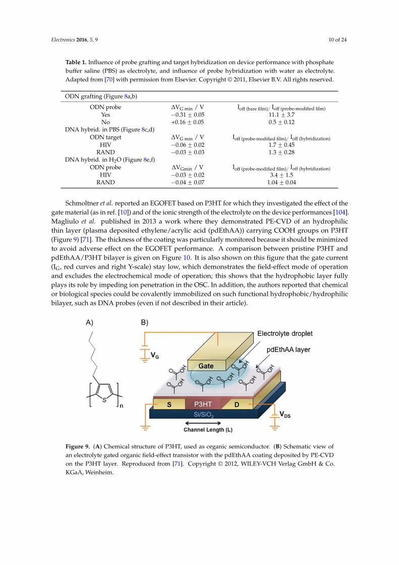
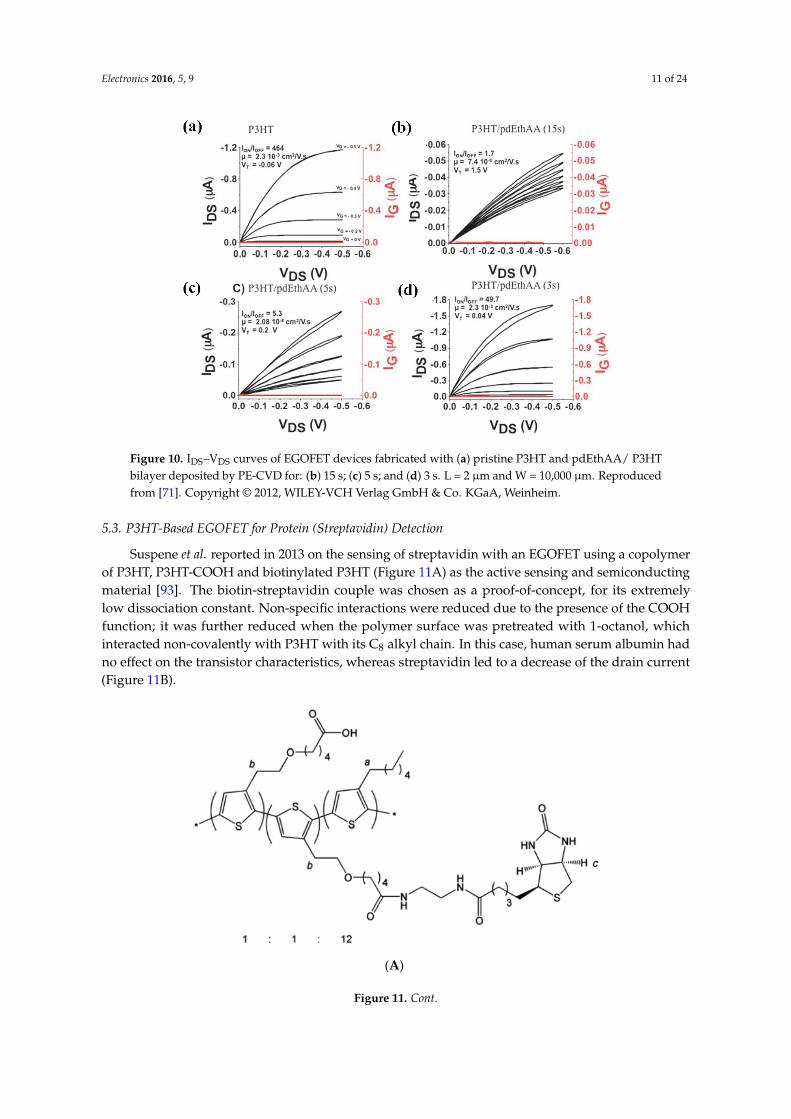
Schmoltner et al. reported an EGOFET based on P3HT for which they investigated the effect of thegate material (as in ref. [10]) and of the ionic strength of the electrolyte on the device performances [104].Magliulo et al. published in 2013 a work where they demonstrated PE-CVD of an hydrophilicthin layer (plasma deposited ethylene/acrylic acid (pdEthAA)) carrying COOH groups on P3HT(Figure 9) [71]. The thickness of the coating was particularly monitored because it should be minimizedto avoid adverse effect on the EGOFET performance. A comparison between pristine P3HT andpdEthAA/P3HT bilayer is given on Figure 10. It is also shown on this figure that the gate current(IG, red curves and right Y-scale) stay low, which demonstrates the field-effect mode of operationand excludes the electrochemical mode of operation; this shows that the hydrophobic layer fullyplays its role by impeding ion penetration in the OSC. In addition, the authors reported that chemicalor biological species could be covalently immobilized on such functional hydrophobic/hydrophilicbilayer, such as DNA probes (even if not described in their article).
Electronics 2016, 5, 9 10 of 23
Table 1. Influence of probe grafting and target hybridization on device performance with phosphate buffer saline (PBS) as electrolyte, and influence of probe hybridization with water as electrolyte. Adapted from [70] with permission from Elsevier. Copyright © 2011, Elsevier B.V. All rights reserved.
ODN grafting (Figure 8a,b)
ODN probe ∆VG min / V Ioff (bare film) / Ioff (probe-modified film) Yes −0.31 ± 0.05 11.1 ± 3.7 No +0.16 ± 0.05 0.5 ± 0.12
DNA hybrid. in PBS (Figure 8c,d)
ODN target ∆VG min / V Ioff (probe-modified film) / Ioff (hybridization) HIV −0.06 ± 0.02 1.7 ± 0.45
RAND −0.03 ± 0.03 1.3 ± 0.28 DNA hybrid. in H2O (Figure 8e,f)
ODN probe ∆VGmin / V Ioff (probe-modified film) / Ioff (hybridization) HIV −0.03 ± 0.02 3.4 ± 1.5
RAND −0.04 ± 0.07 1.04 ± 0.04
Schmoltner et al. reported an EGOFET based on P3HT for which they investigated the effect of the gate material (as in ref. [10]) and of the ionic strength of the electrolyte on the device performances [104]. Magliulo et al. published in 2013 a work where they demonstrated PE-CVD of an hydrophilic thin layer (plasma deposited ethylene/acrylic acid (pdEthAA)) carrying COOH groups on P3HT (Figure 9) [71]. The thickness of the coating was particularly monitored because it should be minimized to avoid adverse effect on the EGOFET performance. A comparison between pristine P3HT and pdEthAA/P3HT bilayer is given on Figure 10. It is also shown on this figure that the gate current (IG, red curves and right Y-scale) stay low, which demonstrates the field-effect mode of operation and excludes the electrochemical mode of operation; this shows that the hydrophobic layer fully plays its role by impeding ion penetration in the OSC. In addition, the authors reported that chemical or biological species could be covalently immobilized on such functional hydrophobic/hydrophilic bilayer, such as DNA probes (even if not described in their article).
Figure 9. (A) Chemical structure of P3HT, used as organic semiconductor. (B) Schematic view of an electrolyte gated organic field-effect transistor with the pdEthAA coating deposited by PE-CVD on the P3HT layer. Reproduced from [71]. Copyright © 2012, WILEY-VCH Verlag GmbH & Co. KGaA, Weinheim.
Figure 9. (A) Chemical structure of P3HT, used as organic semiconductor. (B) Schematic view ofan electrolyte gated organic field-effect transistor with the pdEthAA coating deposited by PE-CVDon the P3HT layer. Reproduced from [71]. Copyright © 2012, WILEY-VCH Verlag GmbH & Co.KGaA, Weinheim.
Electronics 2016, 5, 9 11 of 24
Electronics 2016, 5, 9 11 of 23
Figure 10. IDS–VDS curves of EGOFET devices fabricated with (a) pristine P3HT and pdEthAA/ P3HT bilayer deposited by PE-CVD for: (b) 15 s; (c) 5 s; and (d) 3 s. L = 2 μm and W = 10,000 μm. Reproduced from [71]. Copyright © 2012, WILEY-VCH Verlag GmbH & Co. KGaA, Weinheim.
5.3. P3HT-Based EGOFET for Protein (Streptavidin) Detection
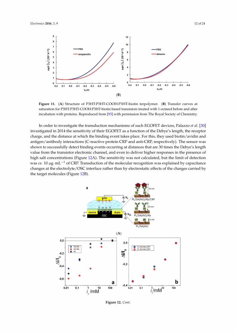
Suspene et al. reported in 2013 on the sensing of streptavidin with an EGOFET using a copolymer of P3HT, P3HT-COOH and biotinylated P3HT (Figure 11A) as the active sensing and semiconducting material [93]. The biotin-streptavidin couple was chosen as a proof-of-concept, for its extremely low dissociation constant. Non-specific interactions were reduced due to the presence of the COOH function; it was further reduced when the polymer surface was pretreated with 1-octanol, which interacted non-covalently with P3HT with its C8 alkyl chain. In this case, human serum albumin had no effect on the transistor characteristics, whereas streptavidin led to a decrease of the drain current (Figure 11B).
(A)
Figure 10. IDS–VDS curves of EGOFET devices fabricated with (a) pristine P3HT and pdEthAA/ P3HTbilayer deposited by PE-CVD for: (b) 15 s; (c) 5 s; and (d) 3 s. L = 2 µm and W = 10,000 µm. Reproducedfrom [71]. Copyright © 2012, WILEY-VCH Verlag GmbH & Co. KGaA, Weinheim.
5.3. P3HT-Based EGOFET for Protein (Streptavidin) Detection
Suspene et al. reported in 2013 on the sensing of streptavidin with an EGOFET using a copolymerof P3HT, P3HT-COOH and biotinylated P3HT (Figure 11A) as the active sensing and semiconductingmaterial [93]. The biotin-streptavidin couple was chosen as a proof-of-concept, for its extremelylow dissociation constant. Non-specific interactions were reduced due to the presence of the COOHfunction; it was further reduced when the polymer surface was pretreated with 1-octanol, whichinteracted non-covalently with P3HT with its C8 alkyl chain. In this case, human serum albumin hadno effect on the transistor characteristics, whereas streptavidin led to a decrease of the drain current(Figure 11B).
Electronics 2016, 5, 9 11 of 23
Figure 10. IDS–VDS curves of EGOFET devices fabricated with (a) pristine P3HT and pdEthAA/ P3HT bilayer deposited by PE-CVD for: (b) 15 s; (c) 5 s; and (d) 3 s. L = 2 μm and W = 10,000 μm. Reproduced from [71]. Copyright © 2012, WILEY-VCH Verlag GmbH & Co. KGaA, Weinheim.
5.3. P3HT-Based EGOFET for Protein (Streptavidin) Detection
Suspene et al. reported in 2013 on the sensing of streptavidin with an EGOFET using a copolymer of P3HT, P3HT-COOH and biotinylated P3HT (Figure 11A) as the active sensing and semiconducting material [93]. The biotin-streptavidin couple was chosen as a proof-of-concept, for its extremely low dissociation constant. Non-specific interactions were reduced due to the presence of the COOH function; it was further reduced when the polymer surface was pretreated with 1-octanol, which interacted non-covalently with P3HT with its C8 alkyl chain. In this case, human serum albumin had no effect on the transistor characteristics, whereas streptavidin led to a decrease of the drain current (Figure 11B).
(A)
Figure 11. Cont.
Electronics 2016, 5, 9 12 of 24Electronics 2016, 5, 9 12 of 23
(B)
Figure 11. (A) Structure of P3HT:P3HT-COOH:P3HT-biotin terpolymer. (B) Transfer curves at saturation for P3HT:P3HT-COOH:P3HT-biotin based transistors treated with 1-octanol before and after incubation with proteins. Reproduced from [93] with permission from The Royal Society of Chemistry.
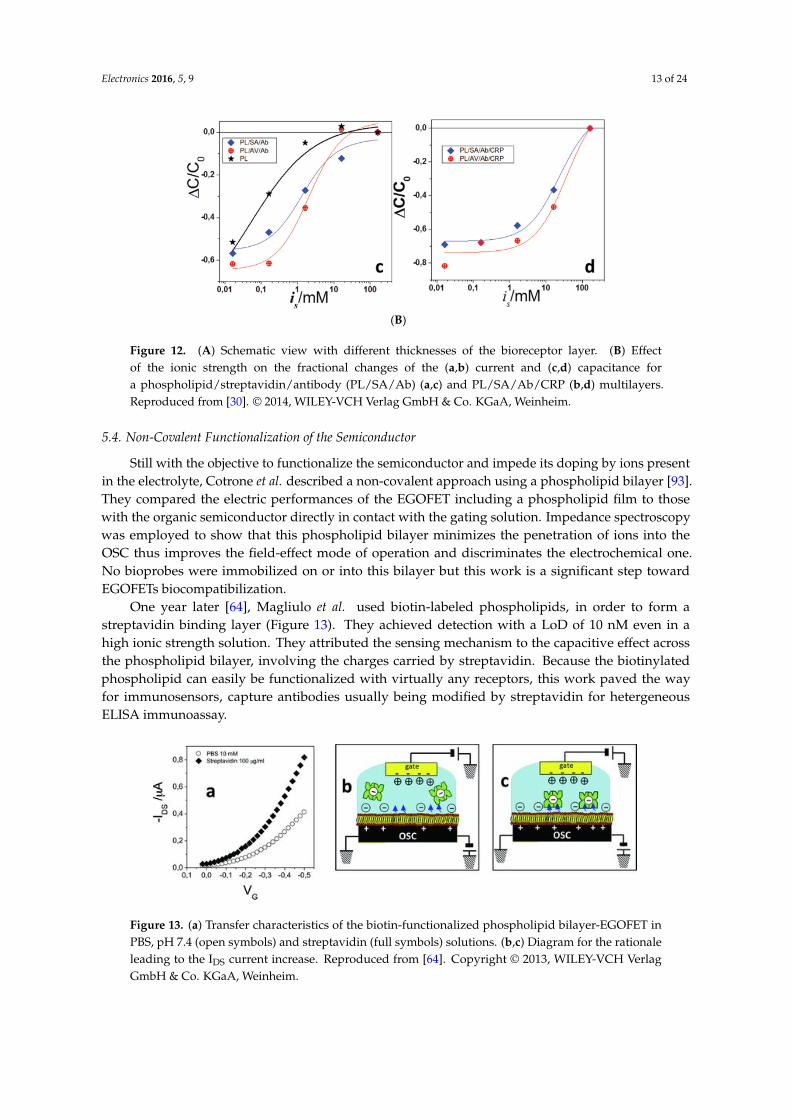
In order to investigate the transduction mechanisms of such EGOFET devices, Palazzo et al. [30] investigated in 2014 the sensitivity of their EGOFET as a function of the Debye’s length, the receptor charge, and the distance at which the binding event takes place. For this, they used biotin/avidin and antigen/antibody interactions (C-reactive protein CRP and anti-CRP, respectively). The sensor was shown to successfully detect binding events occurring at distances that are 30 times the Debye’s length value from the transistor electronic channel, and even to deliver higher responses in the presence of high salt concentrations (Figure 12A). The sensitivity was not calculated, but the limit of detection was ca. 10 μg·mL−1 of CRP. Transduction of the molecular recognition was explained by capacitance changes at the electrolyte/OSC interface rather than by electrostatic effects of the charges carried by the target molecules (Figure 12B).
(A)
Figure 11. (A) Structure of P3HT:P3HT-COOH:P3HT-biotin terpolymer. (B) Transfer curves atsaturation for P3HT:P3HT-COOH:P3HT-biotin based transistors treated with 1-octanol before and afterincubation with proteins. Reproduced from [93] with permission from The Royal Society of Chemistry.
In order to investigate the transduction mechanisms of such EGOFET devices, Palazzo et al. [30]investigated in 2014 the sensitivity of their EGOFET as a function of the Debye’s length, the receptorcharge, and the distance at which the binding event takes place. For this, they used biotin/avidin andantigen/antibody interactions (C-reactive protein CRP and anti-CRP, respectively). The sensor wasshown to successfully detect binding events occurring at distances that are 30 times the Debye’s lengthvalue from the transistor electronic channel, and even to deliver higher responses in the presence ofhigh salt concentrations (Figure 12A). The sensitivity was not calculated, but the limit of detectionwas ca. 10 µg¨ mL´1 of CRP. Transduction of the molecular recognition was explained by capacitancechanges at the electrolyte/OSC interface rather than by electrostatic effects of the charges carried bythe target molecules (Figure 12B).
Electronics 2016, 5, 9 12 of 23
(B)
Figure 11. (A) Structure of P3HT:P3HT-COOH:P3HT-biotin terpolymer. (B) Transfer curves at saturation for P3HT:P3HT-COOH:P3HT-biotin based transistors treated with 1-octanol before and after incubation with proteins. Reproduced from [93] with permission from The Royal Society of Chemistry.
In order to investigate the transduction mechanisms of such EGOFET devices, Palazzo et al. [30] investigated in 2014 the sensitivity of their EGOFET as a function of the Debye’s length, the receptor charge, and the distance at which the binding event takes place. For this, they used biotin/avidin and antigen/antibody interactions (C-reactive protein CRP and anti-CRP, respectively). The sensor was shown to successfully detect binding events occurring at distances that are 30 times the Debye’s length value from the transistor electronic channel, and even to deliver higher responses in the presence of high salt concentrations (Figure 12A). The sensitivity was not calculated, but the limit of detection was ca. 10 μg·mL−1 of CRP. Transduction of the molecular recognition was explained by capacitance changes at the electrolyte/OSC interface rather than by electrostatic effects of the charges carried by the target molecules (Figure 12B).
(A)
Figure 12. Cont.
Electronics 2016, 5, 9 13 of 24
Electronics 2016, 5, 9 13 of 23
(B)
Figure 12. (A) Schematic view with different thicknesses of the bioreceptor layer. (B) Effect of the ionic strength on the fractional changes of the (a,b) current and (c,d) capacitance for a phospholipid/streptavidin/antibody (PL/SA/Ab) (a,c) and PL/SA/Ab/CRP (b,d) multilayers. Reproduced from [30]. © 2014, WILEY-VCH Verlag GmbH & Co. KGaA, Weinheim.
5.4. Non-Covalent Functionalization of the Semiconductor
Still with the objective to functionalize the semiconductor and impede its doping by ions present in the electrolyte, Cotrone et al. described a non-covalent approach using a phospholipid bilayer [93]. They compared the electric performances of the EGOFET including a phospholipid film to those with the organic semiconductor directly in contact with the gating solution. Impedance spectroscopy was employed to show that this phospholipid bilayer minimizes the penetration of ions into the OSC thus improves the field-effect mode of operation and discriminates the electrochemical one. No bioprobes were immobilized on or into this bilayer but this work is a significant step toward EGOFETs biocompatibilization.
One year later [64], Magliulo et al. used biotin-labeled phospholipids, in order to form a streptavidin binding layer (Figure 13). They achieved detection with a LoD of 10 nM even in a high ionic strength solution. They attributed the sensing mechanism to the capacitive effect across the phospholipid bilayer, involving the charges carried by streptavidin. Because the biotinylated phospholipid can easily be functionalized with virtually any receptors, this work paved the way for immunosensors, capture antibodies usually being modified by streptavidin for hetergeneous ELISA immunoassay.
Figure 13. (a) Transfer characteristics of the biotin-functionalized phospholipid bilayer-EGOFET in PBS, pH 7.4 (open symbols) and streptavidin (full symbols) solutions. (b,c) Diagram for the rationale leading to the IDS current increase. Reproduced from [64]. Copyright © 2013, WILEY-VCH Verlag GmbH & Co. KGaA, Weinheim
Figure 12. (A) Schematic view with different thicknesses of the bioreceptor layer. (B) Effectof the ionic strength on the fractional changes of the (a,b) current and (c,d) capacitance fora phospholipid/streptavidin/antibody (PL/SA/Ab) (a,c) and PL/SA/Ab/CRP (b,d) multilayers.Reproduced from [30]. © 2014, WILEY-VCH Verlag GmbH & Co. KGaA, Weinheim.
5.4. Non-Covalent Functionalization of the Semiconductor
Still with the objective to functionalize the semiconductor and impede its doping by ions presentin the electrolyte, Cotrone et al. described a non-covalent approach using a phospholipid bilayer [93].They compared the electric performances of the EGOFET including a phospholipid film to thosewith the organic semiconductor directly in contact with the gating solution. Impedance spectroscopywas employed to show that this phospholipid bilayer minimizes the penetration of ions into theOSC thus improves the field-effect mode of operation and discriminates the electrochemical one.No bioprobes were immobilized on or into this bilayer but this work is a significant step towardEGOFETs biocompatibilization.
One year later [64], Magliulo et al. used biotin-labeled phospholipids, in order to form astreptavidin binding layer (Figure 13). They achieved detection with a LoD of 10 nM even in ahigh ionic strength solution. They attributed the sensing mechanism to the capacitive effect acrossthe phospholipid bilayer, involving the charges carried by streptavidin. Because the biotinylatedphospholipid can easily be functionalized with virtually any receptors, this work paved the wayfor immunosensors, capture antibodies usually being modified by streptavidin for hetergeneousELISA immunoassay.
Electronics 2016, 5, 9 13 of 23
(B)
Figure 12. (A) Schematic view with different thicknesses of the bioreceptor layer. (B) Effect of the ionic strength on the fractional changes of the (a,b) current and (c,d) capacitance for a phospholipid/streptavidin/antibody (PL/SA/Ab) (a,c) and PL/SA/Ab/CRP (b,d) multilayers. Reproduced from [30]. © 2014, WILEY-VCH Verlag GmbH & Co. KGaA, Weinheim.
5.4. Non-Covalent Functionalization of the Semiconductor
Still with the objective to functionalize the semiconductor and impede its doping by ions present in the electrolyte, Cotrone et al. described a non-covalent approach using a phospholipid bilayer [93]. They compared the electric performances of the EGOFET including a phospholipid film to those with the organic semiconductor directly in contact with the gating solution. Impedance spectroscopy was employed to show that this phospholipid bilayer minimizes the penetration of ions into the OSC thus improves the field-effect mode of operation and discriminates the electrochemical one. No bioprobes were immobilized on or into this bilayer but this work is a significant step toward EGOFETs biocompatibilization.
One year later [64], Magliulo et al. used biotin-labeled phospholipids, in order to form a streptavidin binding layer (Figure 13). They achieved detection with a LoD of 10 nM even in a high ionic strength solution. They attributed the sensing mechanism to the capacitive effect across the phospholipid bilayer, involving the charges carried by streptavidin. Because the biotinylated phospholipid can easily be functionalized with virtually any receptors, this work paved the way for immunosensors, capture antibodies usually being modified by streptavidin for hetergeneous ELISA immunoassay.
Figure 13. (a) Transfer characteristics of the biotin-functionalized phospholipid bilayer-EGOFET in PBS, pH 7.4 (open symbols) and streptavidin (full symbols) solutions. (b,c) Diagram for the rationale leading to the IDS current increase. Reproduced from [64]. Copyright © 2013, WILEY-VCH Verlag GmbH & Co. KGaA, Weinheim
Figure 13. (a) Transfer characteristics of the biotin-functionalized phospholipid bilayer-EGOFET inPBS, pH 7.4 (open symbols) and streptavidin (full symbols) solutions. (b,c) Diagram for the rationaleleading to the IDS current increase. Reproduced from [64]. Copyright © 2013, WILEY-VCH VerlagGmbH & Co. KGaA, Weinheim.
Electronics 2016, 5, 9 14 of 24
5.5. pBTTT-Based EGOFET for Protein (Streptavidin) Detection
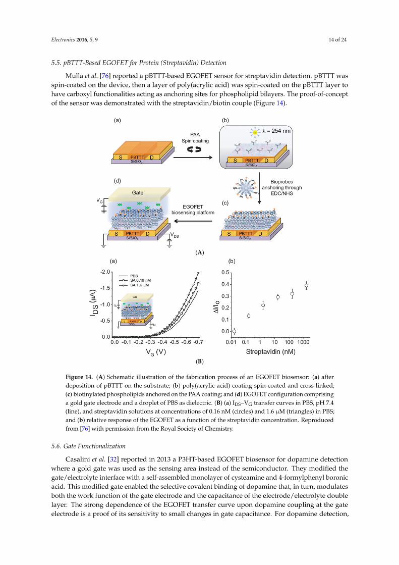
Mulla et al. [76] reported a pBTTT-based EGOFET sensor for streptavidin detection. pBTTT wasspin-coated on the device, then a layer of poly(acrylic acid) was spin-coated on the pBTTT layer tohave carboxyl functionalities acting as anchoring sites for phospholipid bilayers. The proof-of-conceptof the sensor was demonstrated with the streptavidin/biotin couple (Figure 14).
Electronics 2016, 5, 9 14 of 23
5.5. pBTTT-Based EGOFET for Protein (Streptavidin) Detection
Mulla et al. [76] reported a pBTTT-based EGOFET sensor for streptavidin detection. pBTTT was spin-coated on the device, then a layer of poly(acrylic acid) was spin-coated on the pBTTT layer to have carboxyl functionalities acting as anchoring sites for phospholipid bilayers. The proof-of-concept of the sensor was demonstrated with the streptavidin/biotin couple (Figure 14).
(A)
(B)
Figure 14. (A) Schematic illustration of the fabrication process of an EGOFET biosensor: (a) after deposition of pBTTT on the substrate; (b) poly(acrylic acid) coating spin-coated and cross-linked; (c) biotinylated phospholipids anchored on the PAA coating; and (d) EGOFET configuration comprising a gold gate electrode and a droplet of PBS as dielectric. (B) (a) IDS–VG transfer curves in PBS, pH 7.4 (line), and streptavidin solutions at concentrations of 0.16 nM (circles) and 1.6 μM (triangles) in PBS; and (b) relative response of the EGOFET as a function of the streptavidin concentration. Reproduced from [76] with permission from the Royal Society of Chemistry.
5.6. Gate Functionalization
Casalini et al. [32] reported in 2013 a P3HT-based EGOFET biosensor for dopamine detection where a gold gate was used as the sensing area instead of the semiconductor. They modified the gate/electrolyte interface with a self-assembled monolayer of cysteamine and 4-formylphenyl boronic acid. This modified gate enabled the selective covalent binding of dopamine that, in turn, modulates both the work function of the gate electrode and the capacitance of the electrode/electrolyte double layer. The strong dependence of the EGOFET transfer curve upon
Figure 14. (A) Schematic illustration of the fabrication process of an EGOFET biosensor: (a) afterdeposition of pBTTT on the substrate; (b) poly(acrylic acid) coating spin-coated and cross-linked;(c) biotinylated phospholipids anchored on the PAA coating; and (d) EGOFET configuration comprisinga gold gate electrode and a droplet of PBS as dielectric. (B) (a) IDS–VG transfer curves in PBS, pH 7.4(line), and streptavidin solutions at concentrations of 0.16 nM (circles) and 1.6 µM (triangles) in PBS;and (b) relative response of the EGOFET as a function of the streptavidin concentration. Reproducedfrom [76] with permission from the Royal Society of Chemistry.
5.6. Gate Functionalization
Casalini et al. [32] reported in 2013 a P3HT-based EGOFET biosensor for dopamine detectionwhere a gold gate was used as the sensing area instead of the semiconductor. They modified thegate/electrolyte interface with a self-assembled monolayer of cysteamine and 4-formylphenyl boronicacid. This modified gate enabled the selective covalent binding of dopamine that, in turn, modulatesboth the work function of the gate electrode and the capacitance of the electrode/electrolyte doublelayer. The strong dependence of the EGOFET transfer curve upon dopamine coupling at the gateelectrode is a proof of its sensitivity to small changes in gate capacitance. For dopamine detection,
Electronics 2016, 5, 9 15 of 24
the threshold voltage shift was of ca. 50 mV for 0.1 nM dopamine. The selectivity of boronic acid fordopamine was supported by the fact that boronic acid is known to act as a Lewis acid for associationwith vicinal glycols such as sugars or catechol, via formation of a boronate ester. This reaction alsoworks well on dopamine and is therefore specific, providing that no other vicinal diols are present inthe analyzed sample (this reaction has been often reported in the literature dedicated to dopaminesensing since 2013).
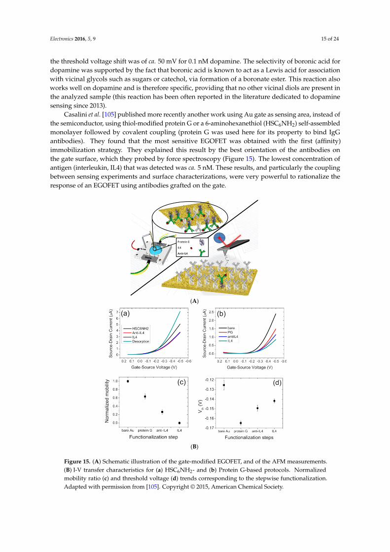
Casalini et al. [105] published more recently another work using Au gate as sensing area, instead ofthe semiconductor, using thiol-modified protein G or a 6-aminohexanethiol (HSC6NH2) self-assembledmonolayer followed by covalent coupling (protein G was used here for its property to bind IgGantibodies). They found that the most sensitive EGOFET was obtained with the first (affinity)immobilization strategy. They explained this result by the best orientation of the antibodies onthe gate surface, which they probed by force spectroscopy (Figure 15). The lowest concentration ofantigen (interleukin, IL4) that was detected was ca. 5 nM. These results, and particularly the couplingbetween sensing experiments and surface characterizations, were very powerful to rationalize theresponse of an EGOFET using antibodies grafted on the gate.
Electronics 2016, 5, 9 15 of 23
dopamine coupling at the gate electrode is a proof of its sensitivity to small changes in gate capacitance. For dopamine detection, the threshold voltage shift was of ca. 50 mV for 0.1 nM dopamine. The selectivity of boronic acid for dopamine was supported by the fact that boronic acid is known to act as a Lewis acid for association with vicinal glycols such as sugars or catechol, via formation of a boronate ester. This reaction also works well on dopamine and is therefore specific, providing that no other vicinal diols are present in the analyzed sample (this reaction has been often reported in the literature dedicated to dopamine sensing since 2013).
Casalini et al. [105] published more recently another work using Au gate as sensing area, instead of the semiconductor, using thiol-modified protein G or a 6-aminohexanethiol (HSC6NH2) self-assembled monolayer followed by covalent coupling (protein G was used here for its property to bind IgG antibodies). They found that the most sensitive EGOFET was obtained with the first (affinity) immobilization strategy. They explained this result by the best orientation of the antibodies on the gate surface, which they probed by force spectroscopy (Figure 15). The lowest concentration of antigen (interleukin, IL4) that was detected was ca. 5 nM. These results, and particularly the coupling between sensing experiments and surface characterizations, were very powerful to rationalize the response of an EGOFET using antibodies grafted on the gate.
(A)
(B)
Figure 15. (A) Schematic illustration of the gate-modified EGOFET, and of the AFM measurements. (B) I-V transfer characteristics for (a) HSC6NH2- and (b) Protein G-based protocols. Normalized mobility ratio (c) and threshold voltage (d) trends corresponding to the stepwise functionalization. Adapted with permission from [105]. Copyright © 2015, American Chemical Society.
Figure 15. (A) Schematic illustration of the gate-modified EGOFET, and of the AFM measurements.(B) I-V transfer characteristics for (a) HSC6NH2- and (b) Protein G-based protocols. Normalizedmobility ratio (c) and threshold voltage (d) trends corresponding to the stepwise functionalization.Adapted with permission from [105]. Copyright © 2015, American Chemical Society.
Electronics 2016, 5, 9 16 of 24
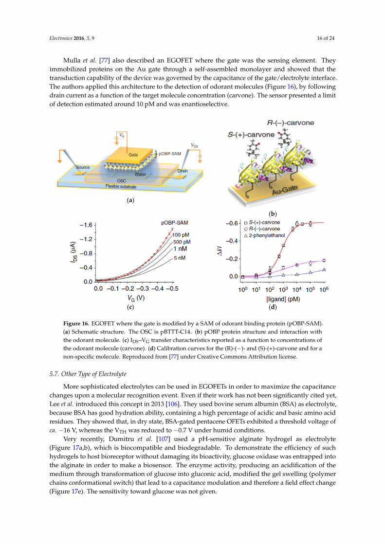
Mulla et al. [77] also described an EGOFET where the gate was the sensing element. Theyimmobilized proteins on the Au gate through a self-assembled monolayer and showed that thetransduction capability of the device was governed by the capacitance of the gate/electrolyte interface.The authors applied this architecture to the detection of odorant molecules (Figure 16), by followingdrain current as a function of the target molecule concentration (carvone). The sensor presented a limitof detection estimated around 10 pM and was enantioselective.
Electronics 2016, 5, 9 16 of 23
Mulla et al. [77] also described an EGOFET where the gate was the sensing element. They immobilized proteins on the Au gate through a self-assembled monolayer and showed that the transduction capability of the device was governed by the capacitance of the gate/electrolyte interface. The authors applied this architecture to the detection of odorant molecules (Figure 16), by following drain current as a function of the target molecule concentration (carvone). The sensor presented a limit of detection estimated around 10 pM and was enantioselective.
(a)
(b)
(c) (d)
Figure 16. EGOFET where the gate is modified by a SAM of odorant binding protein (pOBP-SAM). (a) Schematic structure. The OSC is pBTTT-C14. (b) pOBP protein structure and interaction with the odorant molecule. (c) IDS–VG transfer characteristics reported as a function to concentrations of the odorant molecule (carvone). (d) Calibration curves for the (R)-(−)- and (S)-(+)-carvone and for a non-specific molecule. Reproduced from [77] under Creative Commons Attribution license.
5.7. Other Type of Electrolyte
More sophisticated electrolytes can be used in EGOFETs in order to maximize the capacitance changes upon a molecular recognition event. Even if their work has not been significantly cited yet, Lee et al. introduced this concept in 2013 [106]. They used bovine serum albumin (BSA) as electrolyte, because BSA has good hydration ability, containing a high percentage of acidic and basic amino acid residues. They showed that, in dry state, BSA-gated pentacene OFETs exhibited a threshold voltage of ca. −16 V, whereas the VTH was reduced to −0.7 V under humid conditions.
Very recently, Dumitru et al. [107] used a pH-sensitive alginate hydrogel as electrolyte (Figure 17a,b), which is biocompatible and biodegradable. To demonstrate the efficiency of such hydrogels to host bioreceptor without damaging its bioactivity, glucose oxidase was entrapped into the alginate in order to make a biosensor. The enzyme activity, producing an acidification of the medium through transformation of glucose into gluconic acid, modified the gel swelling (polymer chains conformational switch) that lead to a capacitance modulation and therefore a field effect change (Figure 17e). The sensitivity toward glucose was not given.
Figure 16. EGOFET where the gate is modified by a SAM of odorant binding protein (pOBP-SAM).(a) Schematic structure. The OSC is pBTTT-C14. (b) pOBP protein structure and interaction withthe odorant molecule. (c) IDS–VG transfer characteristics reported as a function to concentrations ofthe odorant molecule (carvone). (d) Calibration curves for the (R)-(´)- and (S)-(+)-carvone and for anon-specific molecule. Reproduced from [77] under Creative Commons Attribution license.
5.7. Other Type of Electrolyte
More sophisticated electrolytes can be used in EGOFETs in order to maximize the capacitancechanges upon a molecular recognition event. Even if their work has not been significantly cited yet,Lee et al. introduced this concept in 2013 [106]. They used bovine serum albumin (BSA) as electrolyte,because BSA has good hydration ability, containing a high percentage of acidic and basic amino acidresidues. They showed that, in dry state, BSA-gated pentacene OFETs exhibited a threshold voltage ofca. ´16 V, whereas the VTH was reduced to ´0.7 V under humid conditions.
Very recently, Dumitru et al. [107] used a pH-sensitive alginate hydrogel as electrolyte(Figure 17a,b), which is biocompatible and biodegradable. To demonstrate the efficiency of suchhydrogels to host bioreceptor without damaging its bioactivity, glucose oxidase was entrapped intothe alginate in order to make a biosensor. The enzyme activity, producing an acidification of themedium through transformation of glucose into gluconic acid, modified the gel swelling (polymerchains conformational switch) that lead to a capacitance modulation and therefore a field effect change(Figure 17e). The sensitivity toward glucose was not given.
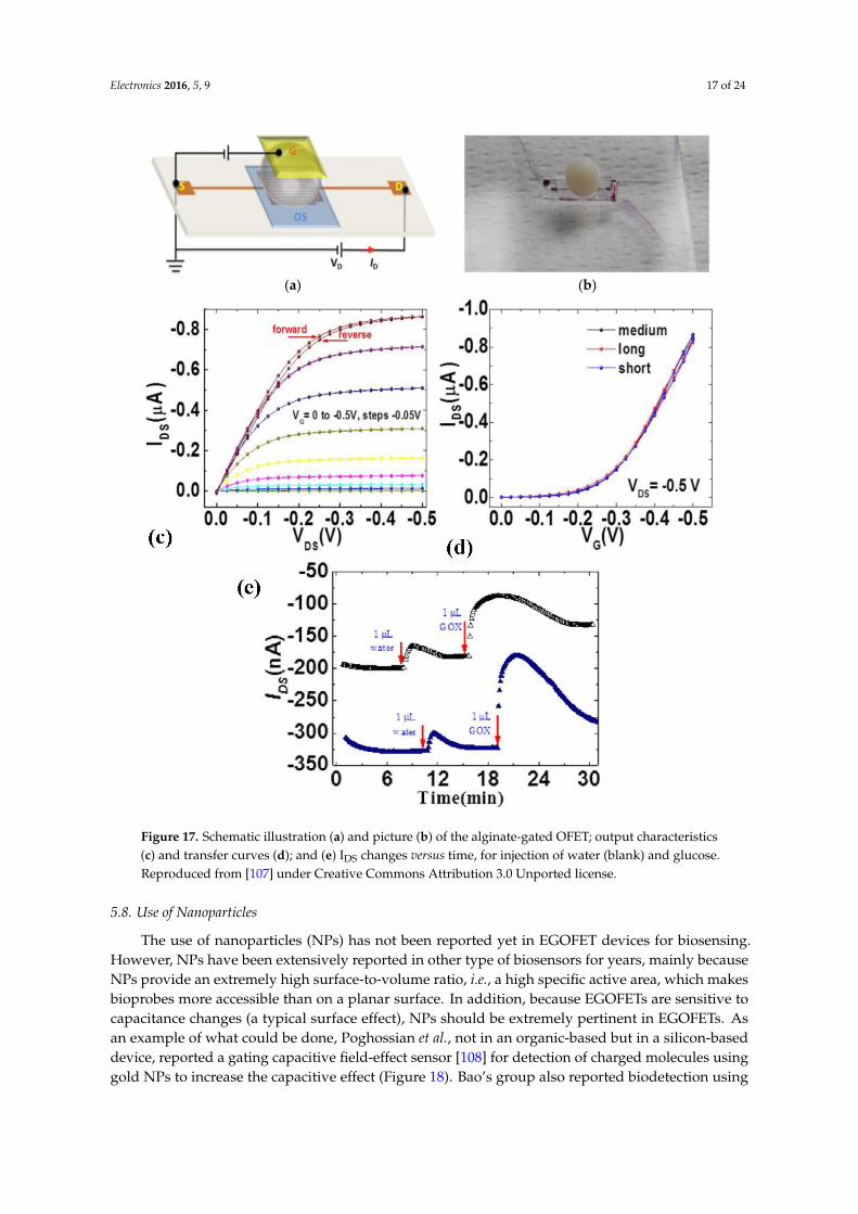
Electronics 2016, 5, 9 17 of 24
Electronics 2016, 5, 9 17 of 23
(a)
(b)
Figure 17. Schematic illustration (a) and picture (b) of the alginate-gated OFET; output characteristics (c) and transfer curves (d); and (e) IDS changes versus time, for injection of water (blank) and glucose. Reproduced from [107] under Creative Commons Attribution 3.0 Unported license.
5.8. Use of Nanoparticles
The use of nanoparticles (NPs) has not been reported yet in EGOFET devices for biosensing. However, NPs have been extensively reported in other type of biosensors for years, mainly because NPs provide an extremely high surface-to-volume ratio, i.e., a high specific active area, which makes bioprobes more accessible than on a planar surface. In addition, because EGOFETs are sensitive to capacitance changes (a typical surface effect), NPs should be extremely pertinent in EGOFETs. As an example of what could be done, Poghossian et al., not in an organic-based but in a silicon-based device, reported a gating capacitive field-effect sensor [108] for detection of charged molecules using gold NPs to increase the capacitive effect (Figure 18). Bao’s group also reported biodetection using a classical bottom-gate OFET decorated with gold nanoparticles, which were used to vary spacing between receptors [109].
Figure 17. Schematic illustration (a) and picture (b) of the alginate-gated OFET; output characteristics(c) and transfer curves (d); and (e) IDS changes versus time, for injection of water (blank) and glucose.Reproduced from [107] under Creative Commons Attribution 3.0 Unported license.
5.8. Use of Nanoparticles
The use of nanoparticles (NPs) has not been reported yet in EGOFET devices for biosensing.However, NPs have been extensively reported in other type of biosensors for years, mainly becauseNPs provide an extremely high surface-to-volume ratio, i.e., a high specific active area, which makesbioprobes more accessible than on a planar surface. In addition, because EGOFETs are sensitive tocapacitance changes (a typical surface effect), NPs should be extremely pertinent in EGOFETs. Asan example of what could be done, Poghossian et al., not in an organic-based but in a silicon-baseddevice, reported a gating capacitive field-effect sensor [108] for detection of charged molecules usinggold NPs to increase the capacitive effect (Figure 18). Bao’s group also reported biodetection using
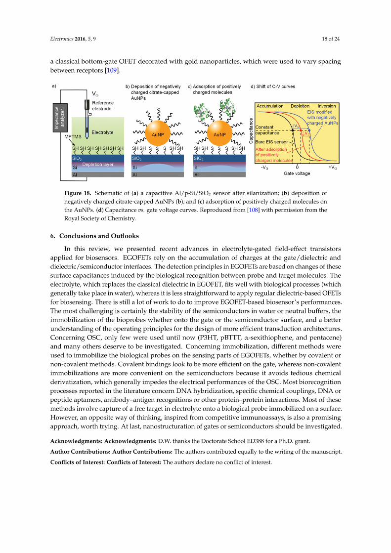
Electronics 2016, 5, 9 18 of 24
a classical bottom-gate OFET decorated with gold nanoparticles, which were used to vary spacingbetween receptors [109].Electronics 2016, 5, 9 18 of 23
Figure 18. Schematic of (a) a capacitive Al/p-Si/SiO2 sensor after silanization; (b) deposition of negatively charged citrate-capped AuNPs (b); and (c) adsorption of positively charged molecules on the AuNPs. (d) Capacitance vs. gate voltage curves. Reproduced from [108] with permission from the Royal Society of Chemistry.
6. Conclusions and Outlooks
In this review, we presented recent advances in electrolyte-gated field-effect transistors applied for biosensors. EGOFETs rely on the accumulation of charges at the gate/dielectric and dielectric/semiconductor interfaces. The detection principles in EGOFETs are based on changes of these surface capacitances induced by the biological recognition between probe and target molecules. The electrolyte, which replaces the classical dielectric in EGOFET, fits well with biological processes (which generally take place in water), whereas it is less straightforward to apply regular dielectric-based OFETs for biosensing. There is still a lot of work to do to improve EGOFET-based biosensor’s performances. The most challenging is certainly the stability of the semiconductors in water or neutral buffers, the immobilization of the bioprobes whether onto the gate or the semiconductor surface, and a better understanding of the operating principles for the design of more efficient transduction architectures. Concerning OSC, only few were used until now (P3HT, pBTTT, α-sexithiophene, and pentacene) and many others deserve to be investigated. Concerning immobilization, different methods were used to immobilize the biological probes on the sensing parts of EGOFETs, whether by covalent or non-covalent methods. Covalent bindings look to be more efficient on the gate, whereas non-covalent immobilizations are more convenient on the semiconductors because it avoids tedious chemical derivatization, which generally impedes the electrical performances of the OSC. Most biorecognition processes reported in the literature concern DNA hybridization, specific chemical couplings, DNA or peptide aptamers, antibody–antigen recognitions or other protein–protein interactions. Most of these methods involve capture of a free target in electrolyte onto a biological probe immobilized on a surface. However, an opposite way of thinking, inspired from competitive immunoassays, is also a promising approach, worth trying. At last, nanostructuration of gates or semiconductors should be investigated.
Acknowledgments: D.W. thanks the Doctorate School ED388 for a Ph.D. grant.
Author Contributions: The authors contributed equally to the writing of the manuscript.
Conflicts of Interest: The authors declare no conflict of interest.
References
1. Wilkinson, A.; McNaught, A.D. IUPAC Compendium of Chemical Terminology, (the “Gold Book”); Blackwell Scientific Publications: Oxford, UK, 1997.
2. Nic, M.; Jirat, J.; Kosata, B. Compendium of Chemical Terminology; Blackwell Scientific Publications: Oxford, UK, 1997. Aviliable online: http://goldbook.iupac.org (accessed on 23 Feburary 2016)
3. Thévenot, D.R.; Toth, K.; Durst, R.A.; Wilson, G.S. Electrochemical biosensors: Recommended definitions and classification. Biosens. Bioelectron. 2001, 16, 121–131.
Figure 18. Schematic of (a) a capacitive Al/p-Si/SiO2 sensor after silanization; (b) deposition ofnegatively charged citrate-capped AuNPs (b); and (c) adsorption of positively charged molecules onthe AuNPs. (d) Capacitance vs. gate voltage curves. Reproduced from [108] with permission from theRoyal Society of Chemistry.
6. Conclusions and Outlooks
In this review, we presented recent advances in electrolyte-gated field-effect transistorsapplied for biosensors. EGOFETs rely on the accumulation of charges at the gate/dielectric anddielectric/semiconductor interfaces. The detection principles in EGOFETs are based on changes of thesesurface capacitances induced by the biological recognition between probe and target molecules. Theelectrolyte, which replaces the classical dielectric in EGOFET, fits well with biological processes (whichgenerally take place in water), whereas it is less straightforward to apply regular dielectric-based OFETsfor biosensing. There is still a lot of work to do to improve EGOFET-based biosensor’s performances.The most challenging is certainly the stability of the semiconductors in water or neutral buffers, theimmobilization of the bioprobes whether onto the gate or the semiconductor surface, and a betterunderstanding of the operating principles for the design of more efficient transduction architectures.Concerning OSC, only few were used until now (P3HT, pBTTT, α-sexithiophene, and pentacene)and many others deserve to be investigated. Concerning immobilization, different methods wereused to immobilize the biological probes on the sensing parts of EGOFETs, whether by covalent ornon-covalent methods. Covalent bindings look to be more efficient on the gate, whereas non-covalentimmobilizations are more convenient on the semiconductors because it avoids tedious chemicalderivatization, which generally impedes the electrical performances of the OSC. Most biorecognitionprocesses reported in the literature concern DNA hybridization, specific chemical couplings, DNA orpeptide aptamers, antibody–antigen recognitions or other protein–protein interactions. Most of thesemethods involve capture of a free target in electrolyte onto a biological probe immobilized on a surface.However, an opposite way of thinking, inspired from competitive immunoassays, is also a promisingapproach, worth trying. At last, nanostructuration of gates or semiconductors should be investigated.
Acknowledgments: Acknowledgments: D.W. thanks the Doctorate School ED388 for a Ph.D. grant.
Author Contributions: Author Contributions: The authors contributed equally to the writing of the manuscript.
Conflicts of Interest: Conflicts of Interest: The authors declare no conflict of interest.
Electronics 2016, 5, 9 19 of 24
References
1. Wilkinson, A.; McNaught, A.D. IUPAC Compendium of Chemical Terminology, (the “Gold Book”); BlackwellScientific Publications: Oxford, UK, 1997.
2. Nic, M.; Jirat, J.; Kosata, B. Compendium of Chemical Terminology; Blackwell Scientific Publications: Oxford,UK, 1997; Available online: http://goldbook.iupac.org (accessed on 23 Feburary 2016).
3. Thévenot, D.R.; Toth, K.; Durst, R.A.; Wilson, G.S. Electrochemical biosensors: Recommended definitionsand classification. Biosens. Bioelectron. 2001, 16, 121–131. [CrossRef]
4. Clark, L.C.; Lyons, C. Electrode systems for continuous monitoring in cardiovascular surgery. Ann. N. Y.Acad. Sci. 1962, 102, 29–45. [CrossRef] [PubMed]
5. Amos, S.W.; James, M. Principles of Transistor Circuits; Butterworths: London, UK, 1984.6. Strakosas, X.; Bongo, M.; Owens, R.M. The organic electrochemical transistor for biological applications.
J. Appl. Polym. Sci. 2015, 132. [CrossRef]7. Sarkar, D.; Banerjee, K. Proposal for tunnel-field-effect-transistor as ultra-sensitive and label-free biosensors.
Appl. Phys. Lett. 2012, 100, 143108. [CrossRef]8. Kergoat, L.; Piro, B.; Berggren, M.; Horowitz, G.; Pham, M.-C. Advances in organic transistor-based
biosensors: From organic electrochemical transistors to electrolyte-gated organic field-effect transistors. Anal.Bioanal. Chem. 2012, 402, 1813–1826. [CrossRef] [PubMed]
9. Tsumura, A.; Koezuka, H.; Ando, T. Macromolecular electronic device: Field-effect transistor with apolythiophene thin film. Appl. Phys. Lett. 1986, 49, 1210–1212. [CrossRef]
10. Kergoat, L.; Herlogsson, L.; Braga, D.; Piro, B.; Pham, M.C.; Crispin, X.; Berggren, M.; Horowitz, G. Awater-gate organic field-effect transistor. Adv. Mater. 2010, 22, 2565–2569. [CrossRef] [PubMed]
11. Buth, F.; Donner, A.; Sachsenhauser, M.; Stutzmann, M.; Garrido, J.A. Biofunctional electrolyte-gated organicfield-effect transistors. Adv. Mater. 2012, 24, 4511–4517. [CrossRef] [PubMed]
12. Dhoot, A.S.; Yuen, J.D.; Heeney, M.; McCulloch, I.; Moses, D.; Heeger, A.J. Beyond the metal-insulatortransition in polymer electrolyte gated polymer field-effect transistors. Proc. Natl. Acad. Sci. USA 2006, 103,11834–11837. [CrossRef] [PubMed]
13. Tarabella, G.; Mohammadi, F.M.; Coppedè, N.; Barbero, F.; Iannotta, S.; Santato, C.; Cicoira, F. Newopportunities for organic electronics and bioelectronics: Ions in action. Chem. Sci. 2013, 4, 1395–1409.[CrossRef]
14. Kim, S.H.; Hong, K.; Xie, W.; Lee, K.H.; Zhang, S.; Lodge, T.P.; Frisbie, C.D. Electrolyte-gated transistors fororganic and printed electronics. Adv. Mater. 2013, 25, 1822–1846. [CrossRef] [PubMed]
15. Yuen, J.D.; Dhoot, A.S.; Namdas, E.B.; Coates, N.E.; Heeney, M.; McCulloch, I.; Moses, D.; Heeger, A.J.Electrochemical doping in electrolyte-gated polymer transistors. J. Am. Chem. Soc. 2007, 129, 14367–14371.[CrossRef] [PubMed]
16. Lee, J.; Kaake, L.G.; Cho, J.H.; Zhu, X.-Y.; Lodge, T.P.; Frisbie, C.D. Ion gel-gated polymer thin-film transistors:Operating mechanism and characterization of gate dielectric capacitance, switching speed, and stability.J. Phys. Chem. C 2009, 113, 8972–8981. [CrossRef]
17. Stern, E.; Klemic, J.F.; Routenberg, D.A.; Wyrembak, P.N.; Turner-Evans, D.B.; Hamilton, A.D.; LaVan, D.A.;Fahmy, T.M.; Reed, M.A. Label-free immunodetection with cmos-compatible semiconducting nanowires.Nature 2007, 445, 519–522. [CrossRef] [PubMed]
18. Stern, E.; Wagner, R.; Sigworth, F.J.; Breaker, R.; Fahmy, T.M.; Reed, M.A. Importance of the debye screeninglength on nanowire field effect transistor sensors. Nano Lett. 2007, 7, 3405–3409. [CrossRef] [PubMed]
19. Liao, C.; Yan, F. Organic semiconductors in organic thin-film transistor-based chemical and biological sensors.Polym. Rev. 2013, 53, 352–406. [CrossRef]
20. Said, E.; Crispin, X.; Herlogsson, L.; Elhag, S.; Robinson, N.D.; Berggren, M. Polymer field-effect transistorgated via a poly (styrenesulfonic acid) thin film. Appl. Phys. Lett. 2006, 89, 143507. [CrossRef]
21. Herlogsson, L.; Crispin, X.; Robinson, N.D.; Sandberg, M.; Hagel, O.J.; Gustafsson, G.; Berggren, M.Low-voltage polymer field-effect transistors gated via a proton conductor. Adv. Mater. 2007, 19, 97–101.[CrossRef]
22. Said, E.; Larsson, O.; Berggren, M.; Crispin, X. Effects of the ionic currents in electrolyte-gated organicfield-effect transistors. Adv. Funct. Mater. 2008, 18, 3529–3536. [CrossRef]
Electronics 2016, 5, 9 20 of 24
23. Ono, S.; Miwa, K.; Seki, S.; Takeya, J. A comparative study of organic single-crystal transistors gated withvarious ionic-liquid electrolytes. Appl. Phys. Lett. 2009, 94, 063301. [CrossRef]
24. Xia, Y.; Cho, J.H.; Lee, J.; Ruden, P.P.; Frisbie, C.D. Comparison of the mobility-carrier density relation inpolymer and single-crystal organic transistors employing vacuum and liquid gate dielectrics. Adv. Mater.2009, 21, 2174–2179. [CrossRef]
25. Hamedi, M.; Herlogsson, L.; Crispin, X.; Marcilla, R.; Berggren, M.; Inganäs, O. Fiber-embeddedelectrolyte-gated field-effect transistors for e-textiles. Adv. Mater. 2009, 21, 573–577. [CrossRef] [PubMed]
26. Lee, J.; Panzer, M.J.; He, Y.; Lodge, T.P.; Frisbie, C.D. Ion gel gated polymer thin-film transistors. J. Am. Chem.Soc. 2007, 129, 4532–4533. [CrossRef] [PubMed]
27. Cho, J.H.; Lee, J.; Xia, Y.; Kim, B.; He, Y.; Renn, M.J.; Lodge, T.P.; Frisbie, C.D. Printable ion-gel gate dielectricsfor low-voltage polymer thin-film transistors on plastic. Nat. Mater. 2008, 7, 900–906. [CrossRef] [PubMed]
28. Cho, J.H.; Lee, J.; He, Y.; Kim, B.; Lodge, T.P.; Frisbie, C.D. High-capacitance ion gel gate dielectrics withfaster polarization response times for organic thin film transistors. Adv. Mater. 2008, 20, 686–690. [CrossRef]
29. Facchetti, A. Dielectric materials: Gels excel. Nat. Mater. 2008, 7, 839–840. [CrossRef] [PubMed]30. Palazzo, G.; De Tullio, D.; Magliulo, M.; Mallardi, A.; Intranuovo, F.; Mulla, M.Y.; Favia, P.;
Vikholm-Lundin, I.; Torsi, L. Detection beyond debye’s length with an electrolyte-gated organic field-effecttransistor. Adv. Mater. 2014, 27, 911–916. [CrossRef] [PubMed]
31. Belkhir, A. Contribution à la Modélisation des Transistors Organiques. Ph.D. Thesis, The University of ReimsChampagne-Ardenne, Reims, France, 2009.
32. Casalini, S.; Leonardi, F.; Cramer, T.; Biscarini, F. Organic field-effect transistor for label-free dopaminesensing. Org. Electron. 2013, 14, 156–163. [CrossRef]
33. Cai, B.; Wang, S.; Huang, L.; Ning, Y.; Zhang, Z.; Zhang, G.-J. Ultrasensitive label-free detection of PNA-DNAhybridization by reduced graphene oxide field-effect transistor biosensor. ACS Nano 2014, 8, 2632–2638.[CrossRef] [PubMed]
34. Vasu, K.; Chakraborty, B.; Sampath, S.; Sood, A. Probing top-gated field effect transistor of reduced grapheneoxide monolayer made by dielectrophoresis. Solid State Commun. 2010, 150, 1295–1298. [CrossRef]
35. Liao, R.; Tang, Z.; Lei, Y.; Guo, B. Polyphenol-reduced graphene oxide: Mechanism and derivatization.J. Phys. Chem. C 2011, 115, 20740–20746. [CrossRef]
36. Liu, F.; Kim, Y.H.; Cheon, D.S.; Seo, T.S. Micropatterned reduced graphene oxide based field-effect transistorfor real-time virus detection. Sens. Actuators B Chem. 2013, 186, 252–257. [CrossRef]
37. Zhao, Y.; Wei, Q.; Xu, C.; Li, H.; Wu, D.; Cai, Y.; Mao, K.; Cui, Z.; Du, B. Label-free electrochemicalimmunosensor for sensitive detection of kanamycin. Sens. Actuators B Chem. 2011, 155, 618–625. [CrossRef]
38. Chen, T.-Y.; Loan, P.T.K.; Hsu, C.-L.; Lee, Y.-H.; Wang, J.T.-W.; Wei, K.-H.; Lin, C.-T.; Li, L.-J. Label-freedetection of DNA hybridization using transistors based on cvd grown graphene. Biosens. Bioelectron. 2013,41, 103–109. [CrossRef] [PubMed]
39. Park, J.W.; Lee, C.; Jang, J. High-performance field-effect transistor-type glucose biosensor based onnanohybrids of carboxylated polypyrrole nanotube wrapped graphene sheet transducer. Sens. Actuators BChem. 2015, 208, 532–537. [CrossRef]
40. Williams, G.; Kamat, P.V. Graphene-semiconductor nanocomposites: Excited-state interactions between znonanoparticles and graphene oxide†. Langmuir 2009, 25, 13869–13873. [CrossRef] [PubMed]
41. Feng, L.; Chen, Y.; Ren, J.; Qu, X. A graphene functionalized electrochemical aptasensor for selective label-freedetection of cancer cells. Biomaterials 2011, 32, 2930–2937. [CrossRef] [PubMed]
42. Ohno, Y.; Maehashi, K.; Yamashiro, Y.; Matsumoto, K. Electrolyte-gated graphene field-effect transistors fordetecting ph and protein adsorption. Nano Lett. 2009, 9, 3318–3322. [CrossRef] [PubMed]
43. Tran, H.; Piro, B.; Reisberg, S.; Nguyen, L.H.; Nguyen, T.D.; Duc, H.; Pham, M. An electrochemical elisa-likeimmunosensor for mirnas detection based on screen-printed gold electrodes modified with reduced grapheneoxide and carbon nanotubes. Biosens. Bioelectron. 2014, 62, 25–30. [CrossRef] [PubMed]
44. Dong, X.; Shi, Y.; Huang, W.; Chen, P.; Li, L.J. Electrical detection of DNA hybridization with single-basespecificity using transistors based on cvd-grown graphene sheets. Adv. Mater. 2010, 22, 1649–1653. [CrossRef][PubMed]
45. Ge, S.; Lan, F.; Yu, F.; Yu, J. Applications of graphene and related nanomaterials in analytical chemistry. NewJ. Chem. 2015, 39, 2380–2395. [CrossRef]
Electronics 2016, 5, 9 21 of 24
46. Tran, H.; Piro, B.; Reisberg, S.; Duc, H.; Pham, M. Antibodies directed to rna/DNA hybrids: Anelectrochemical immunosensor for micrornas detection using graphene-composite electrodes. Anal. Chem.2013, 85, 8469–8474. [CrossRef] [PubMed]
47. Yan, F.; Zhang, M.; Li, J. Solution-gated graphene transistors for chemical and biological sensors. Adv. Healthc.Mater. 2014, 3, 313–331. [CrossRef] [PubMed]
48. Sarkar, D.; Liu, W.; Xie, X.; Anselmo, A.C.; Mitragotri, S.; Banerjee, K. MoS2 Field-Effect Transistor forNext-Generation Label-Free Biosensors. ACS Nano 2014, 8, 3992–4003. [CrossRef] [PubMed]
49. Kergoat, L.; Herlogsson, L.; Piro, B.; Pham, M.C.; Horowitz, G.; Crispin, X.; Berggren, M. Tuning the thresholdvoltage in electrolyte-gated organic field-effect transistors. Proc. Natl. Acad. Sci. USA 2012, 109, 8394–8399.[CrossRef] [PubMed]
50. Fabiano, S.; Braun, S.; Fahlman, M.; Crispin, X.; Berggren, M. Effect of gate electrode work-function on sourcecharge injection in electrolyte-gated organic field-effect transistors. Adv. Funct. Mater. 2014, 24, 695–700.[CrossRef]
51. Demelas, M.; Lai, S.; Spanu, A.; Martinoia, S.; Cosseddu, P.; Barbaro, M.; Bonfiglio, A. Charge sensing byorganic charge-modulated field effect transistors: Application to the detection of bio-related effects. J. Mater.Chem. B 2013, 1, 3811–3819. [CrossRef]
52. Myers, J.D.; Xue, J. Organic semiconductors and their applications in photovoltaic devices. Polym. Rev. 2012,52, 1–37. [CrossRef]
53. Alberga, D.; Mangiatordi, G.F.; Torsi, L.; Lattanzi, G. Effects of annealing and residual solvents on amorphousp3ht and pbttt films. J. Phys. Chem. C 2014, 118, 8641–8655. [CrossRef]
54. Sirringhaus, H.; Brown, P.; Friend, R.; Nielsen, M.M.; Bechgaard, K.; Langeveld-Voss, B.; Spiering, A.;Janssen, R.A.; Meijer, E.; Herwig, P. Two-dimensional charge transport in self-organized, high-mobilityconjugated polymers. Nature 1999, 401, 685–688. [CrossRef]
55. Derby, B. Inkjet printing of functional and structural materials: Fluid property requirements, feature stability,and resolution. Annu. Rev. Mater. Res. 2010, 40, 395–414. [CrossRef]
56. De Gans, B.J.; Duineveld, P.C.; Schubert, U.S. Inkjet printing of polymers: State of the art and futuredevelopments. Adv. Mater. 2004, 16, 203–213. [CrossRef]
57. Liu, C.; Xu, Y.; Liu, Z.; Tsao, H.N.; Müllen, K.; Minari, T.; Noh, Y.-Y.; Sirringhaus, H. Improvingsolution-processed n-type organic field-effect transistors by transfer-printed metal/semiconductor andsemiconductor/semiconductor heterojunctions. Org. Electron. 2014, 15, 1884–1889. [CrossRef]
58. Noh, Y.-Y.; Zhao, N.; Caironi, M.; Sirringhaus, H. Downscaling of self-aligned, all-printed polymer thin-filmtransistors. Nat. Nanotechnol. 2007, 2, 784–789. [CrossRef] [PubMed]
59. Sinno, H.; Nguyen, H.T.; Hägerström, A.; Fahlman, M.; Lindell, L.; Coulembier, O.; Dubois, P.; Crispin, X.;Engquist, I.; Berggren, M. Amphiphilic semiconducting copolymer as compatibility layer for printingpolyelectrolyte-gated ofets. Org. Electron. 2013, 14, 790–796. [CrossRef]
60. Wang, X.; Nilsson, D.; Norberg, P. Printable microfluidic systems using pressure sensitive adhesive materialfor biosensing devices. Biochim. Biophys. Acta 2013, 1830, 4398–4401. [CrossRef] [PubMed]
61. Thiemann, S.; Sachnov, S.; Gruber, M.; Gannott, F.; Spallek, S.; Schweiger, M.; Krückel, J.; Kaschta, J.;Spiecker, E.; Wasserscheid, P. Spray-coatable ionogels based on silane-ionic liquids for low voltage, flexible,electrolyte-gated organic transistors. J. Mater. Chem. C 2014, 2, 2423–2430. [CrossRef]
62. Buth, F.; Kumar, D.; Stutzmann, M.; Garrido, J. Electrolyte-gated organic field-effect transistors for sensingapplications. Appl. Phys. Lett. 2011, 98, 153302. [CrossRef]
63. Scarpa, G.; Idzko, A.; Götz, S.; Neumaier, T.; Thalhammer, S. Biocompatibility studies of solution-processableorganic thin-film transistors for sensing applications. In Proceedings of the IEEE International Conference onNano/Molecular Medicine and Engineering (NANOMED), Tainan, Taiwan, 18–21 October 2009; pp. 265–268.
64. Magliulo, M.; Mallardi, A.; Mulla, M.Y.; Cotrone, S.; Pistillo, B.R.; Favia, P.; Vikholm-Lundin, I.;Palazzo, G.; Torsi, L. Electrolyte-gated organic field-effect transistor sensors based on supported biotinylatedphospholipid bilayer. Adv. Mater. 2013, 25, 2090–2094. [CrossRef] [PubMed]
65. Sokolov, A.N.; Roberts, M.E.; Bao, Z. Fabrication of low-cost electronic biosensors. Mater. Today 2009, 12,12–20. [CrossRef]
66. Angione, M.D.; Cotrone, S.; Magliulo, M.; Mallardi, A.; Altamura, D.; Giannini, C.; Cioffi, N.; Sabbatini, L.;Fratini, E.; Baglioni, P. Interfacial electronic effects in functional biolayers integrated into organic field-effecttransistors. Proc. Natl. Acad. Sci. USA 2012, 109, 6429–6434. [CrossRef] [PubMed]
Electronics 2016, 5, 9 22 of 24
67. Yan, F.; Mok, S.M.; Yu, J.; Chan, H.L.; Yang, M. Label-free DNA sensor based on organic thin film transistors.Biosens. Bioelectron. 2009, 24, 1241–1245. [CrossRef] [PubMed]
68. Maddalena, F.; Kuiper, M.J.; Poolman, B.; Brouwer, F.; Hummelen, J.C.; de Leeuw, D.M.; De Boer, B.;Blom, P.W. Organic field-effect transistor-based biosensors functionalized with protein receptors. J. Appl.Phys. 2010, 108, 124501. [CrossRef]
69. Roberts, M.E.; Mannsfeld, S.C.; Queraltó, N.; Reese, C.; Locklin, J.; Knoll, W.; Bao, Z. Water-stable organictransistors and their application in chemical and biological sensors. Proc. Natl. Acad. Sci. USA 2008, 105,12134–12139. [CrossRef] [PubMed]
70. Kergoat, L.; Piro, B.; Berggren, M.; Pham, M.-C.; Yassar, A.; Horowitz, G. DNA detection with a water-gatedorganic field-effect transistor. Org. Electron. 2012, 13, 1–6. [CrossRef]
71. Magliulo, M.; Pistillo, B.R.; Mulla, M.Y.; Cotrone, S.; Ditaranto, N.; Cioffi, N.; Favia, P.; Torsi, L. PE-CVDof hydrophilic-COOH functionalized coatings on electrolyte gated field-effect transistor electronic layers.Plasma Process. Polym. 2013, 10, 102–109. [CrossRef]
72. Cotrone, S.; Ambrico, M.; Toss, H.; Angione, M.D.; Magliulo, M.; Mallardi, A.; Berggren, M.; Palazzo, G.;Horowitz, G.; Ligonzo, T. Phospholipid film in electrolyte-gated organic field-effect transistors. Org. Electron.2012, 13, 638–644. [CrossRef]
73. McCulloch, I.; Heeney, M.; Chabinyc, M.L.; DeLongchamp, D.; Kline, R.J.; Colle, M.; Duffy, W.; Fischer, D.;Gundlach, D.; Hamadani, B.; et al. Semiconducting Thienothiophene Copolymers: Design, Synthesis,Morphology, and Performance in Thin-Film Organic Transistors. Adv. Mater. 2009, 21, 1091–1109. [CrossRef]
74. Minamiki, T.; Minami, T.; Kurita, R.; Niwa, O.; Wakida, S.-I.; Fukuda, K.; Kumaki, D.; Tokito, S. Accurate andreproducible detection of proteins in water using an extended-gate type organic transistor biosensor. Appl.Phys. Lett. 2014, 104, 243703. [CrossRef]
75. Dumitru, L.M.; Manoli, K.; Magliulo, M.; Palazzo, G.; Torsi, L. Low-voltage solid electrolyte-gated ofets forgas sensing applications. Microelectron. J. 2014, 45, 1679–1683. [CrossRef]
76. Mulla, M.; Seshadri, P.; Torsi, L.; Manoli, K.; Mallardi, A.; Ditaranto, N.; Santacroce, M.; Di Franco, C.;Scamarcio, G.; Magliulo, M. Uv crosslinked poly (acrylic acid): A simple method to bio-functionalizeelectrolyte-gated ofet biosensors. J. Mater. Chem. B 2015, 3, 5049–5057. [CrossRef]
77. Mulla, M.Y.; Tuccori, E.; Magliulo, M.; Lattanzi, G.; Palazzo, G.; Persaud, K.; Torsi, L. Capacitance-modulatedtransistor detects odorant binding protein chiral interactions. Nat. Commun. 2015, 6. [CrossRef] [PubMed]
78. Kline, R.J.; McGehee, M.D.; Kadnikova, E.N.; Liu, J.; Frechet, J.M. Controlling the field-effect mobility ofregioregular polythiophene by changing the molecular weight. Adv. Mater. 2003, 15, 1519–1522. [CrossRef]
79. Chang, J.-F.; Sun, B.; Breiby, D.W.; Nielsen, M.M.; Sölling, T.I.; Giles, M.; McCulloch, I.; Sirringhaus, H.Enhanced mobility of poly (3-hexylthiophene) transistors by spin-coating from high-boiling-point solvents.Chem. Mater. 2004, 16, 4772–4776. [CrossRef]
80. Heffner, G.W.; Pearson, D.S. Molecular characterization of poly (3-hexylthiophene). Macromolecules 1991, 24,6295–6299. [CrossRef]
81. Bao, Z.; Dodabalapur, A.; Lovinger, A.J. Soluble and processable regioregular poly (3-hexylthiophene)for thin film field-effect transistor applications with high mobility. Appl. Phys. Lett. 1996, 69, 4108–4110.[CrossRef]
82. Sirringhaus, H.; Tessler, N.; Friend, R.H. Integrated optoelectronic devices based on conjugated polymers.Science 1998, 280, 1741–1744. [CrossRef] [PubMed]
83. Hugger, S.; Thomann, R.; Heinzel, T.; Thurn-Albrecht, T. Semicrystalline morphology in thin films of poly(3-hexylthiophene). Colloid Polym. Sci. 2004, 282, 932–938.
84. Cho, S.; Lee, K.; Yuen, J.; Wang, G.; Moses, D.; Heeger, A.J.; Surin, M.; Lazzaroni, R. Thermalannealing-induced enhancement of the field-effect mobility of regioregular poly (3-hexylthiophene) films.J. Appl. Phys. 2006, 100, 114503. [CrossRef]
85. Gurau, M.C.; Delongchamp, D.M.; Vogel, B.M.; Lin, E.K.; Fischer, D.A.; Sambasivan, S.; Richter, L.J.Measuring molecular order in poly (3-alkylthiophene) thin films with polarizing spectroscopies. Langmuir2007, 23, 834–842. [CrossRef] [PubMed]
86. Alexiadis, O.; Mavrantzas, V.G. All-atom molecular dynamics simulation of temperature effects on thestructural, thermodynamic, and packing properties of the pure amorphous and pure crystalline phases ofregioregular p3ht. Macromolecules 2013, 46, 2450–2467. [CrossRef]
Electronics 2016, 5, 9 23 of 24
87. Mårdalen, J.; Samuelsen, E.J.; Gautun, O.R.; Carlsen, P.H. Chain configuration of poly (3-hexylthiophene) asrevealed by detailed x-ray diffraction studies. Solid State Commun. 1991, 77, 337–339. [CrossRef]
88. Prosa, T.; Winokur, M.; Moulton, J.; Smith, P.; Heeger, A. X-ray structural studies of poly (3-alkylthiophenes):An example of an inverse comb. Macromolecules 1992, 25, 4364–4372. [CrossRef]
89. Marchant, S.; Foot, P. Annealing behaviour of conductive poly (3-hexylthiophene) films. Polymer 1997, 38,1749–1751. [CrossRef]
90. Favia, P.; Sardella, E.; Gristina, R.; d’Agostino, R. Novel plasma processes for biomaterials: Micro-scalepatterning of biomedical polymers. Surf. Coat. Technol. 2003, 169, 707–711. [CrossRef]
91. Kergoat, L.; Battaglini, N.; Miozzo, L.; Piro, B.; Pham, M.-C.; Yassar, A.; Horowitz, G. Use of poly(3-hexylthiophene)/poly (methyl methacrylate)(p3ht/pmma) blends to improve the performance ofwater-gated organic field-effect transistors. Org. Electron. 2011, 12, 1253–1257. [CrossRef]
92. Toss, H.; Suspene, C.; Piro, B.; Yassar, A.; Crispin, X.; Kergoat, L.; Pham, M.-C.; Berggren, M. On the modeof operation in electrolyte-gated thin film transistors based on different substituted polythiophenes. Org.Electron. 2014, 15, 2420–2427. [CrossRef]
93. Suspène, C.; Piro, B.; Reisberg, S.; Pham, M.-C.; Toss, H.; Berggren, M.; Yassar, A.; Horowitz, G.Copolythiophene-based water-gated organic field-effect transistors for biosensing. J. Mater. Chem. B2013, 1, 2090–2097. [CrossRef]
94. Chabinyc, M.L.; Endicott, F.; Vogt, B.D.; DeLongchamp, D.M.; Lin, E.K.; Wu, Y.; Liu, P.; Ong, B.S. Effectsof humidity on unencapsulated poly (thiophene) thin-film transistors. Appl. Phys. Lett. 2006, 88, 113514.[CrossRef]
95. Hoshino, S.; Yoshida, M.; Uemura, S.; Kodzasa, T.; Takada, N.; Kamata, T.; Yase, K. Influence of moistureon device characteristics of polythiophene-based field-effect transistors. J. Appl. Phys. 2004, 95, 5088–5093.[CrossRef]
96. Caronna, T.; Forte, M.; Catellani, M.; Meille, S.V. Photodegradation and photostabilization studies of poly(3-butylthiophene) in the solid state. Chem. Mater. 1997, 9, 991–995. [CrossRef]
97. Manoli, K.; Dumitru, L.M.; Mulla, M.Y.; Magliulo, M.; Franco, C.D.; Santacroce, M.V.; Scamarcio, G.; Torsi, L.A comparative study of the gas sensing behavior in p3ht-and pbttt-based otfts: The influence of filmmorphology and contact electrode position. Sensors 2014, 14, 16869–16880. [CrossRef] [PubMed]
98. Do, K.; Huang, D.M.; Faller, R.; Moulé, A.J. A comparative md study of the local structure of polymersemiconductors p3ht and pbttt. Phys. Chem. Chem. Phys. 2010, 12, 14735–14739. [CrossRef] [PubMed]
99. Porrazzo, R.; Bellani, S.; Luzio, A.; Lanzarini, E.; Caironi, M.; Antognazza, M.R. Improving mobility andelectrochemical stability of a water-gated polymer field-effect transistor. Org. Electron. 2014, 15, 2126–2134.[CrossRef]
100. Al Naim, A.F.; Grell, M. Organic solvents as gate media for thin-film transistors. J. Appl. Phys. 2012, 112,114502. [CrossRef]
101. Cho, E.; Risko, C.; Kim, D.; Gysel, R.; Cates Miller, N.; Breiby, D.W.; McGehee, M.D.; Toney, M.F.; Kline, R.J.;Bredas, J.-L. Three-dimensional packing structure and electronic properties of biaxially oriented poly (2, 5-bis(3-alkylthiophene-2-yl) thieno [3, 2-b] thiophene) films. J. Am. Chem. Soc. 2012, 134, 6177–6190. [CrossRef][PubMed]
102. McCulloch, I.; Heeney, M.; Bailey, C.; Genevicius, K.; MacDonald, I.; Shkunov, M.; Sparrowe, D.; Tierney, S.;Wagner, R.; Zhang, W. Liquid-crystalline semiconducting polymers with high charge-carrier mobility. Nat.Mater. 2006, 5, 328–333. [CrossRef] [PubMed]
103. Tsao, H.N.; Müllen, K. Improving polymer transistor performance via morphology control. Chem. Soc. Rev.2010, 39, 2372–2386. [CrossRef] [PubMed]
104. Schmoltner, K.; Kofler, J.; Klug, A.; List-Kratochvil, E. Electrolyte-gated organic field-effect transistors forsensing in aqueous media. SPIE Proc. 2013. [CrossRef]
105. Casalini, S.; Dumitru, A.C.; Leonardi, F.; Bortolotti, C.A.; Herruzo, E.T.; Campana, A.; de Oliveira, R.F.;Cramer, T.; Garcia, R.; Biscarini, F. Multiscale sensing of antibody-antigen interactions by organic transistorsand single-molecule force spectroscopy. ACS Nano 2015, 9, 5051–5062. [CrossRef] [PubMed]
106. Lee, C.-Y.; Hwang, J.-C.; Chueh, Y.-L.; Chang, T.-H.; Cheng, Y.-Y.; Lyu, P.-C. Hydrated bovine serum albuminas the gate dielectric material for organic field-effect transistors. Org. Electron. 2013, 14, 2645–2651. [CrossRef]
107. Dumitru, L.; Manoli, K.; Magliulo, M.; Ligonzo, T.; Palazzo, G.; Torsi, L. A hydrogel capsule as gate dielectricin flexible organic field-effect transistors. APL Mater. 2015, 3, 014904. [CrossRef]
Electronics 2016, 5, 9 24 of 24
108. Poghossian, A.; Bäcker, M.; Mayer, D.; Schöning, M.J. Gating capacitive field-effect sensors by the charge ofnanoparticle/molecule hybrids. Nanoscale 2015, 7, 1023–1031. [CrossRef] [PubMed]
109. Hammock, M.L.; Knopfmacher, O.; Naab, B.D.; Tok, J.B.H.; Bao, Z. Investigation of Protein DetectionParameters Using Nanofunctionalized Organic Field-Effect Transistors. ACS Nano 2013, 7, 3970–3980.[CrossRef] [PubMed]
© 2016 by the authors; licensee MDPI, Basel, Switzerland. This article is an open accessarticle distributed under the terms and conditions of the Creative Commons by Attribution(CC-BY) license (http://creativecommons.org/licenses/by/4.0/).