power topology – buck converter - ti.com · power topology – buck converter mickael lauer........
TRANSCRIPT
Application ReportSLVA432–August 2010
Power Topology – Buck ConverterMickael Lauer .......................................................................................... PMP-DCS DC/DC Controllers
ABSTRACT
This application report shows a general step-by-step, Type-III compensation design procedure forcurrent-mode, step-down dc/dc converters as well as the PMP5532 design example using the TexasInstruments TPS40055 step-down converter integrated circuit.
This report also illustrates how to achieve high efficiency in a step-down converter using a wide-inputvoltage range. In addition to the Type-III compensation calculation, the report provides the calculationsneeded to estimate the power losses including an example that achieves up to 95% efficiency.
Contents1 Introduction .................................................................................................................. 22 Compensation Loop Design ............................................................................................... 2
2.1 Compensation Networks Basics ................................................................................. 22.2 Design Procedure for Current-Mode, Type-III Compensation Networks ................................... 32.3 Example ............................................................................................................. 4
3 Efficiency ................................................................................................................... 103.1 Power Dissipated in MOSFETs ................................................................................. 113.2 Power Dissipated in Inductor ................................................................................... 123.3 Efficiency Calculation Formula .................................................................................. 133.4 Example ........................................................................................................... 13
4 Tools ........................................................................................................................ 155 Conclusion .................................................................................................................. 15
List of Figures
1 TPS40055 Schematic ...................................................................................................... 2
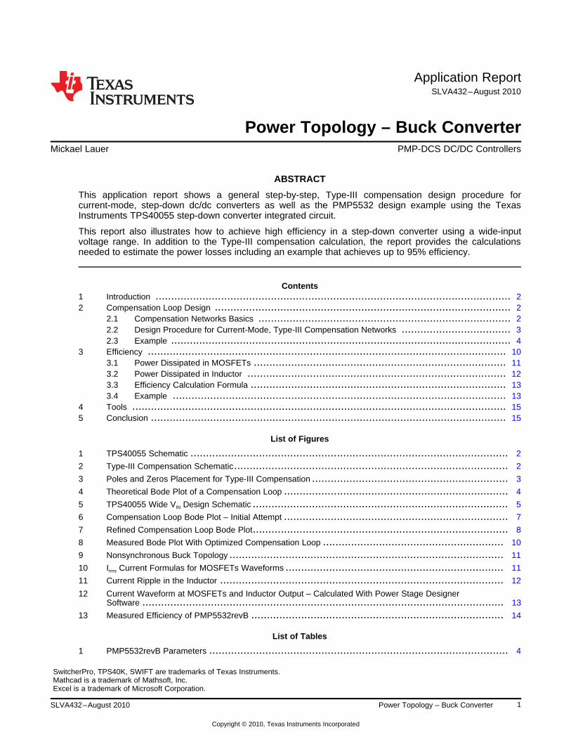
2 Type-III Compensation Schematic........................................................................................ 2
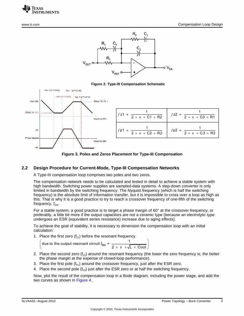
3 Poles and Zeros Placement for Type-III Compensation ............................................................... 3
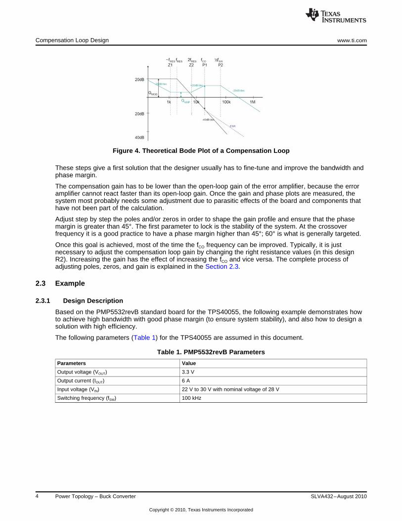
4 Theoretical Bode Plot of a Compensation Loop ........................................................................ 4
5 TPS40055 Wide VIN Design Schematic .................................................................................. 5
6 Compensation Loop Bode Plot – Initial Attempt ........................................................................ 7
7 Refined Compensation Loop Bode Plot.................................................................................. 8
8 Measured Bode Plot With Optimized Compensation Loop .......................................................... 10
9 Nonsynchronous Buck Topology ........................................................................................ 11
10 Irms Current Formulas for MOSFETs Waveforms ...................................................................... 11
11 Current Ripple in the Inductor ........................................................................................... 12
12 Current Waveform at MOSFETs and Inductor Output – Calculated With Power Stage DesignerSoftware .................................................................................................................... 13
13 Measured Efficiency of PMP5532revB ................................................................................. 14
List of Tables
1 PMP5532revB Parameters ................................................................................................ 4
SwitcherPro, TPS40K, SWIFT are trademarks of Texas Instruments.Mathcad is a trademark of Mathsoft, Inc.Excel is a trademark of Microsoft Corporation.
1SLVA432–August 2010 Power Topology – Buck Converter
Copyright © 2010, Texas Instruments Incorporated

Introduction www.ti.com
2 PMP5532revB Bill Of Materials ........................................................................................... 5
3 First Compensation Loop Calculation .................................................................................... 6
4 Final Optimized Pole and Zero Frequencies ............................................................................ 9
5 PMP5532revB Parameters............................................................................................... 13
6 Comparison of Measured and Estimated Efficiency .................................................................. 14
7 Major Sources of Power Losses in Buck Design...................................................................... 14
1 Introduction
The two most commonly used figures of merit for power supplies are efficiency and transient response.Optimizing these two parameters requires proper estimation of the power losses and, usually, the adoptionof Type-III compensation to boost the crossover frequency and phase margin. This exercise is made morecomplex when the voltage translation is large, i.e., from a high-input voltage to a low-output voltage.
This document shows a general, step-by-step calculation and fine tuning of Type-III compensation designfor a current-mode, step-down dc/dc converter as well as the TPS4005x from the TI portfolio. Then, itexplains how to calculate the dissipated power to reach a high efficiency (up to 95%).
The TPS4005x is a family of high-voltage, wide-input (8 V to 40 V), synchronous, step-down controllers. Itoffers design flexibility with a number of useful features such as:
• Input voltage feed forward• Programmable fixed-frequency, voltage-mode operation• Externally synchronizable• Programmable, closed-loop soft start
Figure 1. TPS40055 Schematic
2 Compensation Loop Design
2.1 Compensation Networks Basics
It is possible to improve the transient response of a current-mode dc/dc converter by replacing a Type-IIcompensation scheme with a Type-III to boost the crossover frequency and phase margin. Type-IIIcompensation is simple to design and needs only two extra components compared to a classic Type-IIcompensation. Figure 2 shows the commonly used theoretical Bode plot of Type-III compensation. Theparticular poles and zeros are detailed with the respective formulas in Figure 3.
2 Power Topology – Buck Converter SLVA432–August 2010
Copyright © 2010, Texas Instruments Incorporated
1 1z1 z2
2 C1 R2 2 C3 R1
1 1p1 p2
2 C2 R2 2 C3 R3
» »
´ ´ ´ ´ ´ ´
» »
´ ´ ´ ´ ´ ´
f f
f f
p p
p p
res1
due to the output resonant circuit f =2 L Cout
æ öç ÷
´ ´ ´è øp
www.ti.com Compensation Loop Design
Figure 2. Type-III Compensation Schematic
Figure 3. Poles and Zeros Placement for Type-III Compensation
2.2 Design Procedure for Current-Mode, Type-III Compensation Networks
A Type-III compensation loop comprises two poles and two zeros.
The compensation network needs to be calculated and tested in detail to achieve a stable system withhigh bandwidth. Switching power supplies are sampled-data systems. A step-down converter is onlylimited in bandwidth by the switching frequency. The Nyquist frequency (which is half the switchingfrequency) is the absolute limit of information transfer, but it is impossible to cross over a loop as high asthis. That is why it is a good practice to try to reach a crossover frequency of one-fifth of the switchingfrequency, fSW.
For a stable system, a good practice is to target a phase margin of 60° at the crossover frequency, orpreferably, a little bit more if the output capacitors are not a ceramic type (because an electrolytic typeundergoes an ESR (equivalent series resistance) increase due to aging effects).
To achieve the goal of stability, it is necessary to dimension the compensation loop with an initialcalculation:
1. Place the first zero (fZ1) before the resonant frequency.
2. Place the second zero (fZ2) around the resonant frequency (the lower the zero frequency is, the betterthe phase margin at the expense of closed-loop performance).
3. Place the first pole (fP1) around the crossover frequency, just after the ESR zero.4. Place the second pole (fP2) just after the ESR zero or at half the switching frequency.
Now, plot the result of the compensation loop in a Bode diagram, including the power stage, and add thetwo curves as shown in Figure 4.
3SLVA432–August 2010 Power Topology – Buck Converter
Copyright © 2010, Texas Instruments Incorporated
Compensation Loop Design www.ti.com
Figure 4. Theoretical Bode Plot of a Compensation Loop
These steps give a first solution that the designer usually has to fine-tune and improve the bandwidth andphase margin.
The compensation gain has to be lower than the open-loop gain of the error amplifier, because the erroramplifier cannot react faster than its open-loop gain. Once the gain and phase plots are measured, thesystem most probably needs some adjustment due to parasitic effects of the board and components thathave not been part of the calculation.
Adjust step by step the poles and/or zeros in order to shape the gain profile and ensure that the phasemargin is greater than 45°. The first parameter to lock is the stability of the system. At the crossoverfrequency it is a good practice to have a phase margin higher than 45°; 60° is what is generally targeted.
Once this goal is achieved, most of the time the fCO frequency can be improved. Typically, it is justnecessary to adjust the compensation loop gain by changing the right resistance values (in this designR2). Increasing the gain has the effect of increasing the fCO and vice versa. The complete process ofadjusting poles, zeros, and gain is explained in the Section 2.3.
2.3 Example
2.3.1 Design Description
Based on the PMP5532revB standard board for the TPS40055, the following example demonstrates howto achieve high bandwidth with good phase margin (to ensure system stability), and also how to design asolution with high efficiency.
The following parameters (Table 1) for the TPS40055 are assumed in this document.
Table 1. PMP5532revB Parameters
Parameters Value
Output voltage (VOUT) 3.3 V
Output current (IOUT) 6 A
Input voltage (VIN) 22 V to 30 V with nominal voltage of 28 V
Switching frequency (fSW) 100 kHz
4 Power Topology – Buck Converter SLVA432–August 2010
Copyright © 2010, Texas Instruments Incorporated
www.ti.com Compensation Loop Design
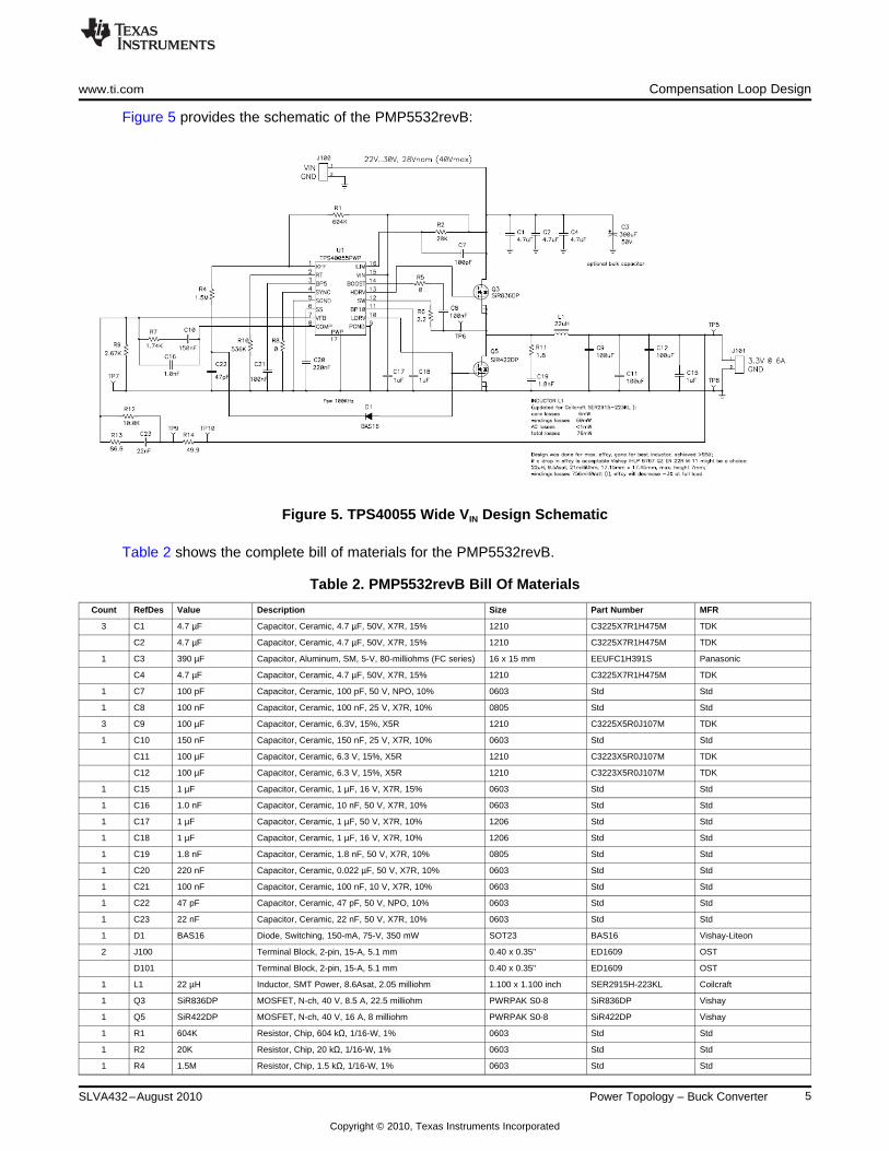
Figure 5 provides the schematic of the PMP5532revB:
Figure 5. TPS40055 Wide VIN Design Schematic
Table 2 shows the complete bill of materials for the PMP5532revB.
Table 2. PMP5532revB Bill Of Materials
Count RefDes Value Description Size Part Number MFR
3 C1 4.7 µF Capacitor, Ceramic, 4.7 µF, 50V, X7R, 15% 1210 C3225X7R1H475M TDK
C2 4.7 µF Capacitor, Ceramic, 4.7 µF, 50V, X7R, 15% 1210 C3225X7R1H475M TDK
1 C3 390 µF Capacitor, Aluminum, SM, 5-V, 80-milliohms (FC series) 16 x 15 mm EEUFC1H391S Panasonic
C4 4.7 µF Capacitor, Ceramic, 4.7 µF, 50V, X7R, 15% 1210 C3225X7R1H475M TDK
1 C7 100 pF Capacitor, Ceramic, 100 pF, 50 V, NPO, 10% 0603 Std Std
1 C8 100 nF Capacitor, Ceramic, 100 nF, 25 V, X7R, 10% 0805 Std Std
3 C9 100 µF Capacitor, Ceramic, 6.3V, 15%, X5R 1210 C3225X5R0J107M TDK
1 C10 150 nF Capacitor, Ceramic, 150 nF, 25 V, X7R, 10% 0603 Std Std
C11 100 µF Capacitor, Ceramic, 6.3 V, 15%, X5R 1210 C3223X5R0J107M TDK
C12 100 µF Capacitor, Ceramic, 6.3 V, 15%, X5R 1210 C3223X5R0J107M TDK
1 C15 1 µF Capacitor, Ceramic, 1 µF, 16 V, X7R, 15% 0603 Std Std
1 C16 1.0 nF Capacitor, Ceramic, 10 nF, 50 V, X7R, 10% 0603 Std Std
1 C17 1 µF Capacitor, Ceramic, 1 µF, 50 V, X7R, 10% 1206 Std Std
1 C18 1 µF Capacitor, Ceramic, 1 µF, 16 V, X7R, 10% 1206 Std Std
1 C19 1.8 nF Capacitor, Ceramic, 1.8 nF, 50 V, X7R, 10% 0805 Std Std
1 C20 220 nF Capacitor, Ceramic, 0.022 µF, 50 V, X7R, 10% 0603 Std Std
1 C21 100 nF Capacitor, Ceramic, 100 nF, 10 V, X7R, 10% 0603 Std Std
1 C22 47 pF Capacitor, Ceramic, 47 pF, 50 V, NPO, 10% 0603 Std Std
1 C23 22 nF Capacitor, Ceramic, 22 nF, 50 V, X7R, 10% 0603 Std Std
1 D1 BAS16 Diode, Switching, 150-mA, 75-V, 350 mW SOT23 BAS16 Vishay-Liteon
2 J100 Terminal Block, 2-pin, 15-A, 5.1 mm 0.40 x 0.35" ED1609 OST
D101 Terminal Block, 2-pin, 15-A, 5.1 mm 0.40 x 0.35" ED1609 OST
1 L1 22 µH Inductor, SMT Power, 8.6Asat, 2.05 milliohm 1.100 x 1.100 inch SER2915H-223KL Coilcraft
1 Q3 SiR836DP MOSFET, N-ch, 40 V, 8.5 A, 22.5 milliohm PWRPAK S0-8 SiR836DP Vishay
1 Q5 SiR422DP MOSFET, N-ch, 40 V, 16 A, 8 milliohm PWRPAK S0-8 SiR422DP Vishay
1 R1 604K Resistor, Chip, 604 kΩ, 1/16-W, 1% 0603 Std Std
1 R2 20K Resistor, Chip, 20 kΩ, 1/16-W, 1% 0603 Std Std
1 R4 1.5M Resistor, Chip, 1.5 kΩ, 1/16-W, 1% 0603 Std Std
5SLVA432–August 2010 Power Topology – Buck Converter
Copyright © 2010, Texas Instruments Incorporated
1C3 =
2 R1 Fz2´ ´ ´p
1C1 =
2 R2 Fz1´ ´ ´p
1R3 =
2 C3 Fp2´ ´ ´p
1C2 =
2 R2 Fp1´ ´ ´p
Compensation Loop Design www.ti.com
Table 2. PMP5532revB Bill Of Materials (continued)Count RefDes Value Description Size Part Number MFR
1 R5 0 Resistor, Chip, 0 Ω, 1/8-W, 5% 0805 Std Std
1 R6 2.2 Resistor, Chip, 0 Ω, 1/8-W, 5% 0805 Std Std
1 R7 1.74K Resistor, Chip, 1.74 kΩ, 1/16-W, 1% 0603 Std Std
1 R8 0 Resistor, Chip, 0 kΩ, 1/16-W, 1% 0603 Std Std
1 R9 2.67K Resistor, Chip, 2.67 kΩ, 1/16-W, 1% 0603 Std Std
1 R10 536K Resistor, Chip, 536 kΩ, 1/16-W, 1% 0603 Std Std
1 R11 1.8 Resistor, Chip, 18 Ω, 1/4-W, 5% 1206 Std Std
1 R12 10.0K Resistor, Chip, 10 kΩ, 1/16-W, 1% 0603 Std Std
1 R13 86.6 Resistor, Chip, 604 Ω, 1/16-W, 1% 0603 Std Std
1 R14 49.9 Resistor, Chip, 49.9 Ω, 1/16-W, 1% 0603 Std Std
4 TP5 Test Point, Red, 1 mm 0.038" 240-345 Farnell
TP6 Test Point, Red, 1 mm 0.038" 240-345 Farnell
2 TP7 Test Point, Black, 1 mm 0.038" 240-333 Farnell
TP8 Test Point, Black, 1 mm 0.038" 240-333 Farnell
TP9 Test Point, Red, 1 mm 0.038" 240-345 Farnell
TP10 Test Point, Red, 1 mm 0.038" 240-345 Farnell
1 U1 TPS40055PWP IC, Wide Input Synchronous Buck Controller PWP16 TPS40051PWP Texas Instruments
Notes: 1. These assemblies are ESD sensitive, ESD precautions shall be observed.
2. These assemblies must be clean and free from flux and all contaminants.Use of no clean flux is not acceptable.
3. These assemblies must comply with workmanship standards IPC-A-610 Class 2.
4. Ref designators marked with an asterisk (**) cannot be substituted.All other components can be substituted with equivalent MFG's components.
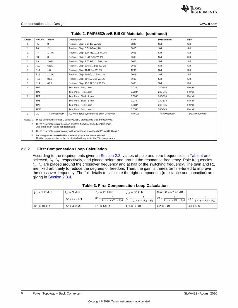
2.3.2 First Compensation Loop Calculation
According to the requirements given in Section 2.2, values of pole and zero frequencies in Table 4 areselected, fZ1, fZ2, respectively, and placed before and around the resonance frequency. Pole frequenciesfp1, fp2 are placed around the crossover frequency and at half of the switching frequency. The gain and R1are fixed arbitrarily to reduce the degrees of freedom. Then, the gain is thereafter fine-tuned to improvethe crossover frequency. The full details to calculate the right components (resistance and capacitor) aregiving in Section 2.3.4.
Table 3. First Compensation Loop Calculation
ƒz1 = 1.2 kHz ƒz2 = 3 kHz ƒp1 = 20 kHz ƒp2 = 50 kHz Gain: 0.4/–7.95 dB
R2 = G × R1
R1 = 10 kΩ R2 = 4.0 kΩ R3 = 640 Ω C1 = 33 nF C2 = 2 nF C3 = 5 nF
6 Power Topology – Buck Converter SLVA432–August 2010
Copyright © 2010, Texas Instruments Incorporated

www.ti.com Compensation Loop Design
Figure 6 shows the Bode gain and phase plots for the complete system including the error amplifier openloop: gain (dark purple), the power stage (gain: red and phase: blue), the compensation (names total; gainblack and phase: black and thin).
Figure 6. Compensation Loop Bode Plot – Initial Attempt
This first estimation achieves a poor crossover frequency of 8.34 kHz with an acceptable phase margin atthe practical limit for production stability of 45.63°. It proves that the foregoing requirements are not aperfect design method, but some empirical rules are useful for the first step in pole and zero placements.
After this first step, the designer has to optimize the location of each pole and zero frequency to adjust thecompensation loop gain to achieve the highest crossover frequency with a comfortable phase margin(around 60°). This is explained in the following paragraphs.
NOTE: Figure 4 was also a theoretical plot; the frequencies behavior illustrated in that figure is notas accurate as that observable in Figure 6.
2.3.3 Second Step: Adjusting Pole and Zero Frequencies
After first deriving a tentative stable system, the designer can now fine-tune the pole and zero frequenciesby several approaches and simulations. As no specific rules apply, this work can be done with andExcel™ or Mathcad™ sheet. The second simulation has been done with this fine-tune procedure toincrease the fCO with a double pole, double zero (in order to simplify the calculations and improve thephase margin):
• 1/50 of fSW for the two zeros, so Fz1 ≈ Fz2 ≈ 2 kHz• Poles around the fSE, so Fp1 ≈ Fp2 ≈ 90 kHz• Gain reduced at 0.6 dB or 1.07 linear
7SLVA432–August 2010 Power Topology – Buck Converter
Copyright © 2010, Texas Instruments Incorporated
Compensation Loop Design www.ti.com
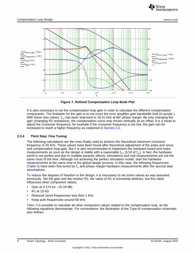
Figure 7. Refined Compensation Loop Bode Plot
It is also necessary to set the compensation loop gain in order to calculate the different compensationcomponents. The limitation for the gain is to not cross the error amplifier gain bandwidth limit (in purple ).With these new values, fCO has been improved to 18.41 kHz at 66° phase margin. By only changing thegain (changing R2 resistance), the compensation curve only moves vertically as an offset. It is a mean toadjust the crossover frequency: for example if the crossover frequency is too low, the gain can beincreased to reach a higher frequency as explained in Section 2.2.
2.3.4 Third Step: Fine Tuning
The following calculations are the ones finally used to achieve the theoretical maximum crossoverfrequency of 20 kHz. These values have been found after theoretical adjustment of the poles and zerosand compensation loop gain. But it is also recommended to implement the hardware board and makemeasurements as soon as the design is stable with a reasonable fCO (1/10 of fsw). In fact, the hardwareworld is not perfect and due to multiple parasitic effects, simulations and real measurements are not thesame most of the time. Although not achieving the perfect simulation model, start the hardwaremeasurements at the same time in the global design process. In this case, the following frequencies(Table 5) have been fine-tuned by fco and phase margin hardware measurements after the second stepassumptions.
To reduce the degrees of freedom in the design, it is necessary to set some values as was assumedpreviously. Set the gain and the resistor R1; the value of R1 is somewhat arbitrary, but this valueinfluences other component values:
• Gain at 0.174 (or –15.18 dB)• R1 at 10 kΩ• Reduced zeros frequencies less than 1 kHz• Keep pole frequencies around 90 kHz
Then, it is possible to calculate all other component values related to the compensation loop, as thefollowing equations demonstrate. For convenience, the illustration of the Type-III compensation schematicalso follows.
8 Power Topology – Buck Converter SLVA432–August 2010
Copyright © 2010, Texas Instruments Incorporated

R2G = , so R2 = G R1
R1
R2 = 0.174 x 10000 = 1740
´
W
1 1p1 , so C2 =
2 x C2 x R2 2 R2 p1
1C2 = 0.99 nF(1nF)
2 1740 92000
»´ ´
=´ ´
ffp p
p
1 1z2 , so C3 =
2 x C2 x R1 2 R1 z2
1C3 = 22.73 nF(22nF)
2 10000 700
»´ ´
=´ ´
ffp p
p
1 1z1 , so C1 =
2 C1 R2 2 R2 z1
1C1 = 0.15 nF(0.15 F)
2 1740 600
»´ ´ ´ ´
=´ ´
ffp p
mp
87-9
1 1p1 , so R3 =
2 C3 R3 2 C3 p2
1R3 = 87.2 ( )
2 22 10 83000
»´ ´ ´ ´
= W W´ ´ ´
ffp p
p
www.ti.com Compensation Loop Design
NOTE: The values given in parenthesis are the real component values, according to the availablestandard values. This limitation brings some difference to the desired poles and zeros inFigure 5.
Calculation of R2:
Calculation of C2:
Calculation of C3:
Calculation of C1:
Calculation of R3:
Table 4. Final Optimized Pole and Zero Frequencies
ƒz1 = 610 Hz ƒz2 = 723 Hz ƒp1 = 91.468 kHz ƒp2 = 83.537 kHz Gain: 0.174/–15.19 dB
9SLVA432–August 2010 Power Topology – Buck Converter
Copyright © 2010, Texas Instruments Incorporated

Efficiency www.ti.com
Figure 8 shows the measured Bode plot of the real circuit implemented on the PMP5532 board. Anoticeable point is the crossing of the gain curve (red) and 0 dB which is the crossover frequency fCO.Here, fCO is 20 kHz perfectly equal to one-fifth of the switching frequency (100 kHz). At this frequency, thesystem is also stable with a phase margin of 60°. However, the simulation achieves a crossover frequencyof 15.08 kHz at a phase margin of 76.4°. This is a good example that shows the difference betweensimulation and real world. As previously explained, simulation can help to derive a first stable system;however, for fine-tuning it is necessary to make real measurements on hardware.
Another important point to check is the slope around fCO (–1, i.e., –20 dB/dec), the gain margin of–10.86dB is also reasonable. Gain margin is the amount of gain necessary to move the 0-dB crossing tooccur at the same frequency as the –180° crossing. The gain margin is the gain on the Bode diagram atthe frequency where the phase plot crosses 0° or –180°.
Figure 8. Measured Bode Plot With Optimized Compensation Loop
3 Efficiency
As previously mentioned, the estimation of efficiency is an important part of power supply design. Thethree main places of power dissipation in a dc-dc converter are:
• MOSFET switching losses (influenced by the turnon and turnoff times of the MOSFETs)• MOSFET conduction losses (directly proportional to the rDS(on) of the MOSFETs)• Inductor conduction losses
– Core losses: Energy loss due to the changing magnetic energy in the core during a switching cycleequals the difference between magnetic energy put into the core during the on-time and themagnetic energy extracted from the core during the off-time.
– Winding losses: Power loss in the windings at dc is due to the windings dc resistance and the RMScurrent through the inductor.
For a greater accuracy, it also possible to include the MOSFET gate charge losses and body diodedissipation, but in this design these are negligible compared to the three losses just mentioned and can beignored in most cases.
10 Power Topology – Buck Converter SLVA432–August 2010
Copyright © 2010, Texas Instruments Incorporated
High Side MOSFET Rectifier MOSFET
www.ti.com Efficiency
3.1 Power Dissipated in MOSFETs
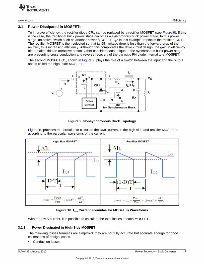
To improve efficiency, the rectifier diode CR1 can be replaced by a rectifier MOSFET (see Figure 9). If thisis the case, the traditional buck power stage becomes a synchronous buck power stage. In this powerstage, an active switch such as another power MOSFET, Q2 in this example, replaces the rectifier, CR1.The rectifier MOSFET is then selected so that its ON voltage drop is less than the forward drop of therectifier, thus increasing efficiency. Although this complicates the drive circuit design, the gain in efficiencyoften makes this an attractive option. Other considerations unique to the synchronous buck power stageare preventing cross-conduction and reverse recovery of the parasitic PN diode internal to a MOSFET.
The second MOSFET Q1, shown in Figure 9, plays the role of a switch between the input and the outputand is called the high- side MOSFET.
Figure 9. Nonsynchronous Buck Topology
Figure 10 provides the formulas to calculate the RMS current in the high-side and rectifier MOSFETsaccording to the particular waveforms of the current.
Figure 10. Irms Current Formulas for MOSFETs Waveforms
With the RMS current, it is possible to calculate the total losses in each MOSFET.
3.1.1 Power Dissipated in High-Side MOSFET
The following losses formulas are simplified; they are not fully accurate but accurate enough for goodestimations of design losses.
• Conduction losses
11SLVA432–August 2010 Power Topology – Buck Converter
Copyright © 2010, Texas Instruments Incorporated
22 I
Irms = Iout +12
D
Efficiency www.ti.com
Pcond = Irms2 × rDS(on)
rDS(on)HS is the on-time, drain-to-source resistance of the high-side MOSFET• Switching losses
Psw = Vin × ƒSW × Iout × (tf + tr)Where ƒSW is the switching frequency of the IC, tf and tr are respectively the falling and rising time ofthe MOSFET.
• Gate charge lossesPqg × Vgate × ƒsw
Where Qg is the MOSFET gate charge and Vgate is the gate to source voltage.
The total power loss is the sum of all foregoing power losses:Pfet = Psww + Pcond + Pqg
3.1.2 Power Dissipated in Rectified MOSFET• Conduction losses
Pcond = Irms2 × rDS(on)
rDS(on) is the on-time, drain-to-source resistance of the high-side MOSFET.• Body diode losses
Pbd = Iout × Vbd × ƒsw × tDELAY
Where ƒSW is the switching frequency of the IC, VDC is the body diode forward voltage; tDELAY is thedelay time just before the SW node rises.
• QG lossesPqg = Qg × Vgate × ƒsw
Where Qg is the MOSFET gate charge.
The total power loss is the sum of all power losses:Pfet = Psw + Pbd + Pqg
No switching losses occur on the rectifier side because when the high-side MOSFET turns off, the rectifieris also off. It is not possible to directly turn on the rectifier side without any delay. At this moment, nocurrent flows through the rectifier; only the body diode of the FET creates a voltage and generates bodydiode losses.
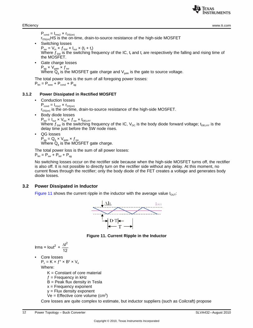
3.2 Power Dissipated in Inductor
Figure 11 shows the current ripple in the inductor with the average value IOUT:
Figure 11. Current Ripple in the Inductor
• Core lossesPc = K × ƒx × By × Ve
Where:K = Constant of core materialƒ = Frequency in kHzB = Peak flux density in Teslax = Frequency exponenty = Flux density exponentVe = Effective core volume (cm3)
Core losses are quite complex to estimate, but inductor suppliers (such as Coilcraft) propose
12 Power Topology – Buck Converter SLVA432–August 2010
Copyright © 2010, Texas Instruments Incorporated

Pout=
Pout + Plh
Rectifier MOSFET High Side MOSFET Inductor
www.ti.com Efficiency
automated calculations on their Web sites.• Winding losses
Psw = Irms2 × DCRWhere DCR is the dc resistance of the inductor.
The total power losses are the sum of all power losses:Pind = Pc + Pw + Pacr
3.3 Efficiency Calculation Formula
Finally, efficiency can be estimated using the following ratio:
With the following assumptions:
Pout = Iout × Vout
Pl = Pfet + Pind which are the total losses of the design.
3.4 Example
Based on the PMP5532reB standard board for the TPS40055, the following example illustrates how todesign a solution with high efficiency.
Assume the parameters listed in (Table 5) for this design.
Table 5. PMP5532revB Parameters
Parameters Value
Output voltage (VOUT) 3.3 V
Output current (IOUT) 6 A
Input voltage (VIN) 22 V to 30 V and nominal voltage of 28 V
Switching frequency (fSW) 100 kHz
In order to calculate the RMS current, it is necessary to know the current waveform at the rectifier,high-side MOSFETs, and inductor. Figure 12 shows the true different waveforms of these components,which were generated by using the Power Stage Designer tool.
Figure 12. Current Waveform at MOSFETs and Inductor Output – Calculated With Power Stage DesignerSoftware
By applying the previous formulas for losses, the estimated efficiency is 96.3%. Table 6 shows the trueefficiency of the design.
13SLVA432–August 2010 Power Topology – Buck Converter
Copyright © 2010, Texas Instruments Incorporated
Efficiency www.ti.com
Table 6. Comparison of Measured and Estimated Efficiency
Estimated Efficiency Measured Efficiency Delta
96.3% 95.3% 1%
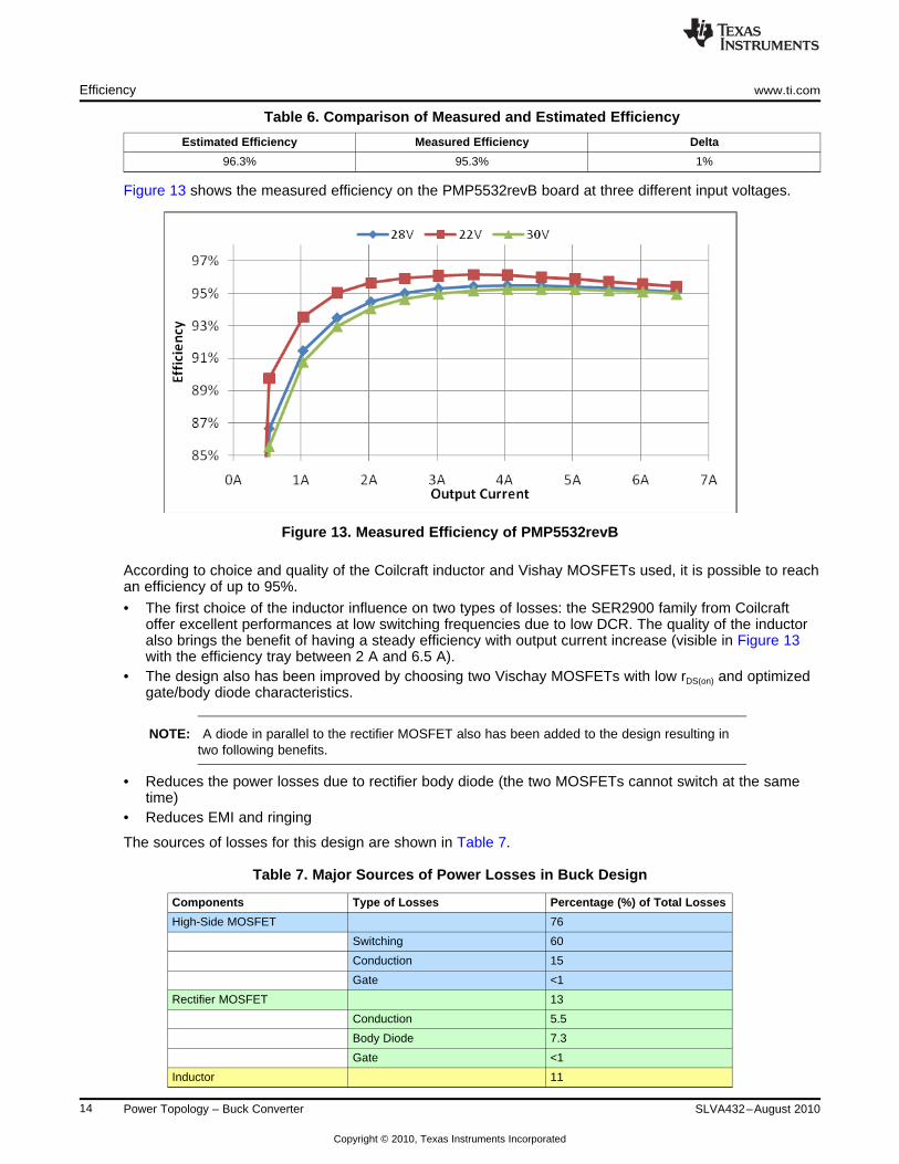
Figure 13 shows the measured efficiency on the PMP5532revB board at three different input voltages.
Figure 13. Measured Efficiency of PMP5532revB
According to choice and quality of the Coilcraft inductor and Vishay MOSFETs used, it is possible to reachan efficiency of up to 95%.
• The first choice of the inductor influence on two types of losses: the SER2900 family from Coilcraftoffer excellent performances at low switching frequencies due to low DCR. The quality of the inductoralso brings the benefit of having a steady efficiency with output current increase (visible in Figure 13with the efficiency tray between 2 A and 6.5 A).
• The design also has been improved by choosing two Vischay MOSFETs with low rDS(on) and optimizedgate/body diode characteristics.
NOTE: A diode in parallel to the rectifier MOSFET also has been added to the design resulting intwo following benefits.
• Reduces the power losses due to rectifier body diode (the two MOSFETs cannot switch at the sametime)
• Reduces EMI and ringing
The sources of losses for this design are shown in Table 7.
Table 7. Major Sources of Power Losses in Buck Design
Components Type of Losses Percentage (%) of Total Losses
High-Side MOSFET 76
Switching 60
Conduction 15
Gate <1
Rectifier MOSFET 13
Conduction 5.5
Body Diode 7.3
Gate <1
Inductor 11
14 Power Topology – Buck Converter SLVA432–August 2010
Copyright © 2010, Texas Instruments Incorporated

www.ti.com Tools
Table 7. Major Sources of Power Losses in Buck Design (continued)
Components Type of Losses Percentage (%) of Total Losses
Winding 10.4
Core 0.6
For this design, losses are mainly generated by high-side switching, which can be improved by finding alow switching gate charge MOSFET. The conduction losses are reasonable due to a choice of goodMOSFETs with a low rds(on). Winding losses also are optimized due to low DCR inductor.
To summarize, for the selection of an inductor and MOSFETs, the important parameters are:
• Low rDS(on) of the rectifier MOSFET• Short rise and fall times for the high-side MOSFET (linked to gate charge)• Low dc resistance of the inductor
The best choice for this design are MOSFETs with low rDS(on), VDS of 40 V and SO8 package. At themoment, the high-performance MOSFETs are the following:
• Infineon Optimos series• Vishay SiR series
4 Tools
The following free, software tools were used to design the example (PMP5532 board) described in thisapplication report:
• TI Power Stage Designer is a tool made by design engineers for design engineers. All thecalculations to determine voltage and current stress for semiconductors and magnetics inside varioustopologies are implemented in a single design.To get this Java application, send an email request to [email protected].
• SwitcherPro™ is design software that allows you to design and simulate power supplies with TexasInstruments TPS40K™ controllers, low-power dc/dc converters, and SWIFT™ (TPS54xxx)point-of-load, step-down dc/dc products. The Web link ishttp://focus.ti.com/docs/toolsw/folders/print/switcherpro.html.
5 Conclusion
This application report shows an easy way to implement a Type-III compensation for current-mode,step-down dc/dc converters. The measurements also illustrate the gap between simulation and real world.
In addition, this report provides a quick and easy method to calculate the efficiency of a buck converter.These procedures provide accurate results and reduce the need to build and test the power supply to getthe efficiency data. It is also helpful in the component selection for reaching the highest efficiency.
15SLVA432–August 2010 Power Topology – Buck Converter
Copyright © 2010, Texas Instruments Incorporated

IMPORTANT NOTICE
Texas Instruments Incorporated and its subsidiaries (TI) reserve the right to make corrections, modifications, enhancements, improvements,and other changes to its products and services at any time and to discontinue any product or service without notice. Customers shouldobtain the latest relevant information before placing orders and should verify that such information is current and complete. All products aresold subject to TI’s terms and conditions of sale supplied at the time of order acknowledgment.
TI warrants performance of its hardware products to the specifications applicable at the time of sale in accordance with TI’s standardwarranty. Testing and other quality control techniques are used to the extent TI deems necessary to support this warranty. Except wheremandated by government requirements, testing of all parameters of each product is not necessarily performed.
TI assumes no liability for applications assistance or customer product design. Customers are responsible for their products andapplications using TI components. To minimize the risks associated with customer products and applications, customers should provideadequate design and operating safeguards.
TI does not warrant or represent that any license, either express or implied, is granted under any TI patent right, copyright, mask work right,or other TI intellectual property right relating to any combination, machine, or process in which TI products or services are used. Informationpublished by TI regarding third-party products or services does not constitute a license from TI to use such products or services or awarranty or endorsement thereof. Use of such information may require a license from a third party under the patents or other intellectualproperty of the third party, or a license from TI under the patents or other intellectual property of TI.
Reproduction of TI information in TI data books or data sheets is permissible only if reproduction is without alteration and is accompaniedby all associated warranties, conditions, limitations, and notices. Reproduction of this information with alteration is an unfair and deceptivebusiness practice. TI is not responsible or liable for such altered documentation. Information of third parties may be subject to additionalrestrictions.
Resale of TI products or services with statements different from or beyond the parameters stated by TI for that product or service voids allexpress and any implied warranties for the associated TI product or service and is an unfair and deceptive business practice. TI is notresponsible or liable for any such statements.
TI products are not authorized for use in safety-critical applications (such as life support) where a failure of the TI product would reasonablybe expected to cause severe personal injury or death, unless officers of the parties have executed an agreement specifically governingsuch use. Buyers represent that they have all necessary expertise in the safety and regulatory ramifications of their applications, andacknowledge and agree that they are solely responsible for all legal, regulatory and safety-related requirements concerning their productsand any use of TI products in such safety-critical applications, notwithstanding any applications-related information or support that may beprovided by TI. Further, Buyers must fully indemnify TI and its representatives against any damages arising out of the use of TI products insuch safety-critical applications.
TI products are neither designed nor intended for use in military/aerospace applications or environments unless the TI products arespecifically designated by TI as military-grade or "enhanced plastic." Only products designated by TI as military-grade meet militaryspecifications. Buyers acknowledge and agree that any such use of TI products which TI has not designated as military-grade is solely atthe Buyer's risk, and that they are solely responsible for compliance with all legal and regulatory requirements in connection with such use.
TI products are neither designed nor intended for use in automotive applications or environments unless the specific TI products aredesignated by TI as compliant with ISO/TS 16949 requirements. Buyers acknowledge and agree that, if they use any non-designatedproducts in automotive applications, TI will not be responsible for any failure to meet such requirements.
Following are URLs where you can obtain information on other Texas Instruments products and application solutions:
Products Applications
Amplifiers amplifier.ti.com Audio www.ti.com/audio
Data Converters dataconverter.ti.com Automotive www.ti.com/automotive
DLP® Products www.dlp.com Communications and www.ti.com/communicationsTelecom
DSP dsp.ti.com Computers and www.ti.com/computersPeripherals
Clocks and Timers www.ti.com/clocks Consumer Electronics www.ti.com/consumer-apps
Interface interface.ti.com Energy www.ti.com/energy
Logic logic.ti.com Industrial www.ti.com/industrial
Power Mgmt power.ti.com Medical www.ti.com/medical
Microcontrollers microcontroller.ti.com Security www.ti.com/security
RFID www.ti-rfid.com Space, Avionics & www.ti.com/space-avionics-defenseDefense
RF/IF and ZigBee® Solutions www.ti.com/lprf Video and Imaging www.ti.com/video
Wireless www.ti.com/wireless-apps
Mailing Address: Texas Instruments, Post Office Box 655303, Dallas, Texas 75265Copyright © 2010, Texas Instruments Incorporated