18289602 buck-converter
TRANSCRIPT

STUDY AND DESIGN OF BUCK CONVERTER
ANIRBAN DASGUPTA & ANTIP GHOSH
ELECTRICAL ENGG., NIT, ROURKELA
ABSTRACT
This project is based on the study and design of a buck converter which is basically a dc-dc converter.
It steps down the voltage which is dc in nature and hence it is used where transformer fails. It also
emphasizes on the study of switched mode power supply. After a detailed study, a matlab code was
written and then it was converted to its corresponding Verilog code using Simulink HDL coder for
hardware implementation.
INTRODUCTION
Over the years as the portable electronics industry progressed, different requirements evolved
such as increased battery lifetime, small and cheap systems, brighter, full-color displays and a
demand for increased talk-time in cellular phones. An ever increasing demand from power
systems has placed power consumption at a premium. To keep up with these demands
engineers have worked towards developing efficient conversion techniques and also have
resulted in the subsequent formal growth of an interdisciplinary field of Power Electronics.
However it comes as no surprise that this new field has offered challenges owing to the unique
combination of three major disciplines of electrical engineering: electronics, power and control.
Why use a switching regulator?
Voltage regulation conventionally has been done by Linear Regulators but slowly is being replaced with Switching Regulators. To realize the importance of a switching regulator we will first compare its efficiency with a linear regulator. The resistance of the linear regulator varies in
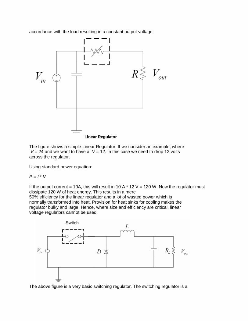
accordance with the load resulting in a constant output voltage.
Linear Regulator
The figure shows a simple Linear Regulator. If we consider an example, where V = 24 and we want to have a V = 12. In this case we need to drop 12 volts
across the regulator.
Using standard power equation:
P = I * V
If the output current = 10A, this will result in 10 A * 12 V = 120 W. Now the regulator must dissipate 120 W of heat energy. This results in a mere 50% efficiency for the linear regulator and a lot of wasted power which is normally transformed into heat. Provision for heat sinks for cooling makes the regulator bulky and large. Hence, where size and efficiency are critical, linear voltage regulators cannot be used.
The above figure is a very basic switching regulator. The switching regulator is a

simple switch (and hence ideally no resistance or very low resistance). This switch goes on and off at a fixed rate (usually between 50 KHz to 100 KHz).
Comparison between Linear & Switching Regulators
DC-DC converters
These are electronic devices that are used whenever we want to change DC electrical power
efficiently from one voltage level to another.We have mentioned the drawbacks of doing this
with a linear regulator and presented the case for SMPS. Generically speaking the use of a
switch or switches for the purpose of power conversion can be regarded as an SMPS.From now
onwards whenever we mention DC-DC converters we shall address them with respect to
SMPS. A few applications of interest of DC-DC converters are where 5V DC on a personal
computer motherboard must be stepped down to 3V, 2V or less for one of the latest CPU chips;
where 1.5V from a single cell must be stepped up to 5V or more, to operate electronic circuitry.
In all of these applications, we want to change the DC energy from one voltage level to another,
while wasting as little as possible in the process. In other words, we want to perform the
conversion with the highest possible efficiency. DC-DC Converters are needed because unlike
AC, DC can’t simply be stepped up or down using a transformer. In many ways, a DC-DC
converter is the DC equivalent of a transformer. They essentially just change the input energy
into a different impedance level. So whatever the output voltage level, the output power all

comes from the input; there’s no energy manufactured inside the converter. Quite the contrary,
in fact some is inevitably used up by the converter circuitry and components, in doing their job.
WHAT ARE SMPS?
High frequency switching converters are power circuits in which the semiconductor devices switch at a rate that is fast compared to the variation of the input and output waveforms.
The figure shows a generic block diagram of a SMPS. The difference between the switching frequency and the frequency of the external waveforms is large enough to permit the use of low-pass filters to remove the unwanted switching frequency components. High frequency switching converters are used most often as interfaces between dc systems of different voltage levels. These converters are known as high-frequency dc/dc converters, and examples of their use are
the power supplies in computers and other electronic equipment. High frequency switching converters can also be used as an interface between dc and ac systems. TYPES OF CONVERTERS
Dc/dc converters can be divided into two broad categories: a) Non-isloated dc/dc converters b) Isolated dc/dc converters
Non-Isolated DC/DC Converters
The non-isolated converter usually employs an inductor, and there is no dc voltage isolation between the input and the output. The vast majority of applications do not require dc isolation between input and output voltages. The non-isolated dc-dc converter has a dc path between its input and output. Battery-based systems that don’t use the ac power line represent a major application for non-isolated dc-dc converters. Isolated DC/DC Converters
For safety considerations, there must be isolation between an electronic system’s ac input and dc output. Typical isolation voltages for ac-dc and dc-dc power supplies run from 1500 to 4000V, depending on the application. Isolated dc-dc converters use a switching transformer whose secondary is either diode-or synchronous-rectified to produce a dc output voltage using an inductor capacitor output filter. This configuration has the advantage of producing multiple output voltages by adding secondary transformer windings. For higher input voltages (48V) transformer isolated converters are more viable.
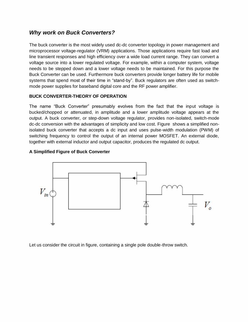
Why work on Buck Converters? The buck converter is the most widely used dc-dc converter topology in power management and
microprocessor voltage-regulator (VRM) applications. Those applications require fast load and
line transient responses and high efficiency over a wide load current range. They can convert a
voltage source into a lower regulated voltage. For example, within a computer system, voltage
needs to be stepped down and a lower voltage needs to be maintained. For this purpose the
Buck Converter can be used. Furthermore buck converters provide longer battery life for mobile
systems that spend most of their time in “stand-by”. Buck regulators are often used as switch-
mode power supplies for baseband digital core and the RF power amplifier.
BUCK CONVERTER-THEORY OF OPERATION
The name “Buck Converter” presumably evolves from the fact that the input voltage is
bucked/chopped or attenuated, in amplitude and a lower amplitude voltage appears at the
output. A buck converter, or step-down voltage regulator, provides non-isolated, switch-mode
dc-dc conversion with the advantages of simplicity and low cost. Figure shows a simplified non-
isolated buck converter that accepts a dc input and uses pulse-width modulation (PWM) of
switching frequency to control the output of an internal power MOSFET. An external diode,
together with external inductor and output capacitor, produces the regulated dc output.
A Simplified Figure of Buck Converter
Let us consider the circuit in figure, containing a single pole double-throw switch.
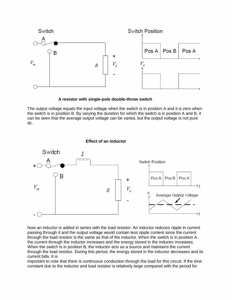
A resistor with single-pole double-throw switch
The output voltage equals the input voltage when the switch is in position A and it is zero when the switch is in position B. By varying the duration for which the switch is in position A and B, it can be seen that the average output voltage can be varied, but the output voltage is not pure dc.
Effect of an inductor
Now an inductor is added in series with the load resistor. An inductor reduces ripple in current passing through it and the output voltage would contain less ripple content since the current through the load resistor is the same as that of the inductor. When the switch is in position A, the current through the inductor increases and the energy stored in the inductor increases. When the switch is in position B, the inductor acts as a source and maintains the current through the load resistor. During this period, the energy stored in the inductor decreases and its current falls. It is important to note that there is continuous conduction through the load for this circuit. If the time constant due to the inductor and load resistor is relatively large compared with the period for

which the switch is in position A or B, then the rise and fall of current through inductor is more or less linear.
Circuit with an LC Filter
Now we add a capacitor across the load resistor and this capacitor reduces the ripple content in voltage across it, whereas an inductor smoothes the current passing through it. The combined action of LC filter reduces the ripple in output to a very low level. It is possible to have a power semiconductor switch to correspond to the switch in position A and a diode in position B. The circuit that results is as shown in the figure below
Buck Converter with Load resistor
When the switch is in position B, the current will pass through the diode. The Buck Converter transfers small packets of energy with the help of a power switch, a diode, and an inductor and is accompanied by an output filter capacitor and input filter. All the other topologies such as the Boost, Buck-Boost Converter etc, vary by the different arrangement of these basic components.

This circuit can be further modified by adding the feedback part which is integral for a SMPS because based on the feedback it stabilizes the output.
Step down switch mode power supply
The PWM Controller compares a portion of the rectified dc output with a voltage reference and varies the PWM duty cycle to maintain a constant dc output voltage. If the output voltage wants to increase, the PWM lowers its duty cycle to reduce the regulated output, keeping it at its proper voltage level. Conversely, if the output voltage tends to go down, the feedback causes the PWM duty cycle to increase and maintain the proper output. A buck converter or step-down switch mode power supply can also be called a switch mode regulator. Purpose of different components in the Buck Converter:-
The Buck converter consists of five standard components:
1. pulse-width modulating controller
2. transistor switch (active switch)
3. diode (passive switch)
4. Capacitor
5. Inductor
DETAILS OF EACH COMPONENT
Switch
In its crudest form a switch can be a toggle switch which switches between supply voltage and ground. But for all practical applications we will deal with transistors. Transistors chosen for use in switching power supplies must have fast switching times and should be able to withstand the voltage spikes produced by the inductor. The input on the gate of the transistor is normally a

Pulse Width Modulated (PWM) signal which will determine the ON and OFF time. Sizing of the power switch is determined by the load current and off-state voltage capability. The power switch (transistor) can either be a MOSFET, IGBT, JFET or a BJT. Power MOSFETs are the key elements of high frequency power systems such as high-density power Supplies. Therefore
MOSFETs have now replaced BJT’s in new designs operating at much higher frequencies but at lower voltages. At high voltages MOSFETs still have their limitations. The intrinsic characteristics of the MOSFET produce a large on-resistance which increases excessively when the devices' breakdown voltage is raised. Therefore, the power MOSFET is only useful up to voltage ratings of 500V and so is restricted to low voltage applications or in two-transistor forward converters and bridge circuits operating off-line. At high breakdown voltages (>200V) the on-state voltage drop of the power MOSFET becomes higher than that of a similar size bipolar device with similar voltage rating. This makes it more attractive to use the bipolar power transistor at the expense of worse high frequency performance. As improvements in fabrication techniques, new materials, device characteristics take place than MOSFETs are likely to replace BJTs. Another new device likely to displace the BJT in many high power applications is the Insulated Gate Bipolar Transistor (IGBT). This device combines the low power drive characteristics of the MOSFET with the low conduction losses and high blocking voltage characteristics of the BJT. Therefore the device is highly suited to high power, high voltage applications. However, since current transport in the device is by the same process as the BJT, its switching speed is much slower than the MOSFET, so the IGBT is at present limited to lower (<50kHz) applications.
Operating Frequency
The operating frequency determines the performance of the switch. Switching frequency
selection is typically determined by efficiency requirements. There is now a growing trend in
research work and new power supply designs in increasing the switching frequencies. The
higher is the switching frequency, the smaller the physical size and component value. The
reason for this is to reduce even further the overall size of the power supply in line with
miniaturization trends in electronic and computer systems. However, there is an upper
frequency limit where either magnetic losses in the inductor or switching losses in the regulator
circuit and power MOSFET reduce efficiency to an impractical level. Higher frequency also
reduces the size of the output capacitor.
Inductor
The function of the inductor is to limit the current slew rate (limit the current in rush) through the
power switch when the circuit is ON. The current through the inductor cannot change suddenly.
When the current through an inductor tends to fall, the inductor tends to maintain the current by
acting as a source. This limits the otherwise high-peak current that would be limited by the
switch resistance alone. The key advantage is when the inductor is used to drop voltage, it
stores energy. Also the inductor controls the percent of the ripple.
Capacitor
Capacitor provides the filtering action by providing a path for the harmonic currents away from
the load. Output capacitance (across the load) is required to minimize the voltage overshoot and
ripple present at the output of a step-down converter. The capacitor is large enough so that its

voltage does not have any noticeable change during the time the switch is off. Large overshoots
are caused by insufficient output capacitance, and large voltage ripple is caused by insufficient
capacitance as well as a high equivalent-series resistance (ESR) in the output capacitor. The
maximum allowed output-voltage overshoot and ripple are usually specified at the time of
design. Thus, to meet the ripple specification for a step-down converter circuit, we must include
an output capacitor with ample capacitance and low ESR.
Freewheeling Diode/Transistor
Since the current in the inductor cannot change suddenly, a path must exist for the inductor
current when the switch is off (open). This path is provided by the freewheeling diode (or catch
diode). The purpose of this diode is not to rectify, but to direct current flow in the circuit and to
ensure that there is always a path for the current to flow into the inductor. It is also necessary
that this diode should be able to turn off relatively fast. Thus the diode enables the converter to
convert stored energy in the inductor to the load. This is a reason why we have higher efficiency
in a DC-DC Converter as compared to a linear regulator. When the switch closes, the current
rises linearly (exponentially if resistance is also present). When the switch opens, the
freewheeling diode causes a linear decrease in current. At steady state we have a saw tooth
response with an average value of the current.
Feedback
Feedback and control circuitry can be carefully nested around these circuits to regulate the
energy transfer and maintain a constant output within normal operating conditions. Control by
pulse-width modulation is necessary for regulating the output. The transistor switch is the heart
of the switched supply and it controls the power supplied to the load.
States of Operation
There are two – the ON State and the OFF State.
ON State
The operation of the buck converter is fairly simple, with an inductor and two switches (usually a
transistor and a diode) that control the inductor. It alternates between connecting the inductor to
source voltage to store energy in the inductor and discharging the inductor into the load.
ON state
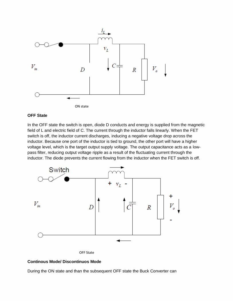
OFF State
In the OFF state the switch is open, diode D conducts and energy is supplied from the magnetic
field of L and electric field of C. The current through the inductor falls linearly. When the FET
switch is off, the inductor current discharges, inducing a negative voltage drop across the
inductor. Because one port of the inductor is tied to ground, the other port will have a higher
voltage level, which is the target output supply voltage. The output capacitance acts as a low-
pass filter, reducing output voltage ripple as a result of the fluctuating current through the
inductor. The diode prevents the current flowing from the inductor when the FET switch is off.
OFF State
Continous Mode/ Discontinuos Mode
During the ON state and than the subsequent OFF state the Buck Converter can

operate in Continuous Mode or Discontinuous Mode. The difference between the two is that in CCM the current in the inductor does not fall to zero.
Current flows continuously in the inductor during the entire switching cycle in steady state operation. In most Buck regulator applications, the inductor current never drops to zero during full-load operation. Overall performance is usually better using continuous mode, and it allows maximum output power to be obtained from a given input voltage and switch current rating. Energy from the battery is supplying the load and is being stored in the inductor L as a magnetic field. The current through the inductor is rising linearly. In the DCM the current in the inductor falls to zero and remains at zero for some portion of the switching cycle. It starts at zero, reaches a peak value, and returns to zero during each switching cycle. In applications where the maximum load current is fairly low, it can be advantageous to design for discontinuous mode operation. In these cases, operating in discontinuous mode can result in a smaller overall converter size (because a smaller inductor can be used). Often the output capacitor must be large to keep the voltage constant.
Synchronous Buck Converters Introduction Synchronous buck converters have received great attention for low-voltage power conversion because of its high efficiency and reduced area consumption. One of the main reasons for not using a synchronous FET earlier was that there was a much greater cost difference between FETs and Schottky diodes years ago. Moreover, since output voltages were generally higher (5V or greater), the drop across the Schottky was not as large a percentage as it is now. As FET technology has improved, providing better and better conductivity at ever lower price, the FET has become the main choice over the Schottky. Even more importantly, the “forward” voltage drop of the FET can be arbitrarily low compared to the Schottky a major issue with output voltages hovering around 1 volt. The synchronous buck topology is also considered suitable for Envelope Tracking Power Supply because of its simple dynamics and symmetrical slewrate Capability.
Topology This topology uses the complementary switches to transfer energy to the filter inductance from the power source.

TThe synchronous buck converter is essentially the same as the buck step-down converter with the substitution of the “catch” diode for another FET switch, or Synchronous Rectifier. The upper MOSFET conducts to transfer energy from the input and charges the inductor current. When the switch control is off, the lower MOSFET switch turns on to circulate the inductor current and provides a current path for the inductor when discharging. The control and driver circuits synchronize the timing of both MOSFETs with the switching frequency. The synchronous PWM control block regulates the output voltage by modulating the conduction intervals of the upper and lower MOSFETs. This topology improves efficiency with faster switch turn-on time and lower FET series resistance versus the diode. Under light loads, the control block usually turns the lower MOSFET off to emulate a diode, this is because more power is lost in turning a large FET switch on and off, than lost due to the resistance of the switch itself.
Problems This topology requires more components and additional switch logic sequencing. Also this power conversion topology suffers from a degraded problem that can severely limit the battery lifetime of portable devices that spend a substantial amount of time in "stand-by" mode and hence resulting in a substantial reduction in converter efficiency. Since many portable devices operate in low-power standby modes for a majority of the time they are on, increasing light-load converter efficiency can significantly increase battery lifetime. The SRBC requires two off-chip passive filter components. These components greatly increase the overall size and cost of the system. Synchronous rectification with discrete MOSFETs causes variable switching delays because of the variations in gate charge and threshold voltage from one MOSFET to another. Standard control circuits compensate for these variations by delaying the turn-on drive of the lower MOSFET until after the gate voltage of the upper MOSFET falls below a threshold. This delay creates a dead time in which neither MOSFET conducts. The dead time eliminates the possibility of a destructive shoot-through condition in which both MOSFETs conduct simultaneously. Standard designs use the same method to delay the turn-on of the upper device.
Improvements Synchronous rectification increases the efficiency of a buck converter by replacing the Schottky diode with a low-side NMOS FET. The resultant voltage drop across the MOSFET can be smaller than the forward voltage drop of the Schottky diode. To show that the efficiency is

greatly increased by replacing the diode with a MOSFET can be shown with the following set of equations. The equation for power loss across a diode can be calculated by:
it is multiplied with (1-D) for the OFF time. Because the diode conducts in the OFF state. Assume that the input is 5V and the output is 3.3 V, and the load current is 10A. In this case the duty cycle will be 66% and the diode will be ON for 34% of the time. A typical diode with a 0.7V would suffer a power loss of 2.38 W. Now we take the equation for a switch
It can be seen that the power loss is very much dependent upon the duty cycle. A synchronous rectifier generally has lower losses than a conventional or Schottky diode, and so its use is quite popular in low voltage DC/DC converters. Also for increased efficiency the following relation must be true
Practical Issues of Buck Converter
Calculation for Duty Ratio For calculation of the duty ratio we will first of all assume that the converter is in steady state. The switches are treated as being ideal, and the losses in the inductive and the capacitive elements are neglected. The analysis also has the assumption that the converter is operating in Continuous conduction mode. Since in steady-state operation waveform must repeat from one time period to the next, the integral of the inductor voltage L v over one time period must be
zero, where Ts= Ton+Toff.

From Figure, it implies that areas A and B must be equal. Therefore,
Calculation for Inductor From Figure (a) we can derive a simplified differential equation based on the assumption that the voltage across the load, and thereby across the capacitor, is fairly constant. The differential equation in terms of the current through the inductor, when the switch is closed, may now be written as

Now, suppose IL is the current prior to closing of switch.
The inductor current increases linearly with time and attains its maximum value
Change in current will be
zs
Let us now analyze the circuit when the switch is in its open position. The inductor current completes its path through the lower side MOSFET and the corresponding differential equation, for 0≤ t ≤ T OFF , is
From the solution of the above first-order differential equation-
Where I L,max is the maximum value of the current in the inductor at the opening
of the switch or the beginning of the off period. As t → T OFF= (1− D)T , the inductor current decreases to its minimum value IL,min such that
Hence,

Graph for inductor current
The average current in the inductor must be equal to the dc current through the load.
The expressions for the maximum and minimum currents through the inductor may now be
written as
The current supplied by the source varies fro ILmin to ILmax during the time the switch is closed
and is zero
otherwise.
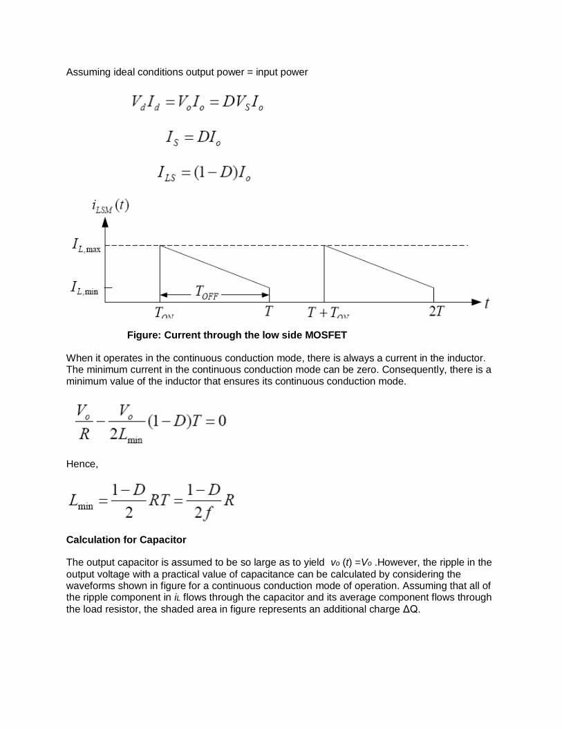
Assuming ideal conditions output power = input power
Figure: Current through the low side MOSFET
When it operates in the continuous conduction mode, there is always a current in the inductor. The minimum current in the continuous conduction mode can be zero. Consequently, there is a minimum value of the inductor that ensures its continuous conduction mode.
Hence,
Calculation for Capacitor
The output capacitor is assumed to be so large as to yield vo (t) =Vo .However, the ripple in the
output voltage with a practical value of capacitance can be calculated by considering the waveforms shown in figure for a continuous conduction mode of operation. Assuming that all of the ripple component in iL flows through the capacitor and its average component flows through
the load resistor, the shaded area in figure represents an additional charge ΔQ.

Peak to peak voltage,
during toff
Where switching frequency fs=1/Ts and
The above equation shows that the voltage ripple can be minimized by selecting a corner frequency fc of the low pass filter at the output such that fc <<fs. Also, the ripple is independent
of the output load power, so long as the converter operates in the continuous-conduction mode. We should note that in switch-mode dc power supplies, the percentage ripple in the output voltage is usually specified to be less than, for instance, 1%.
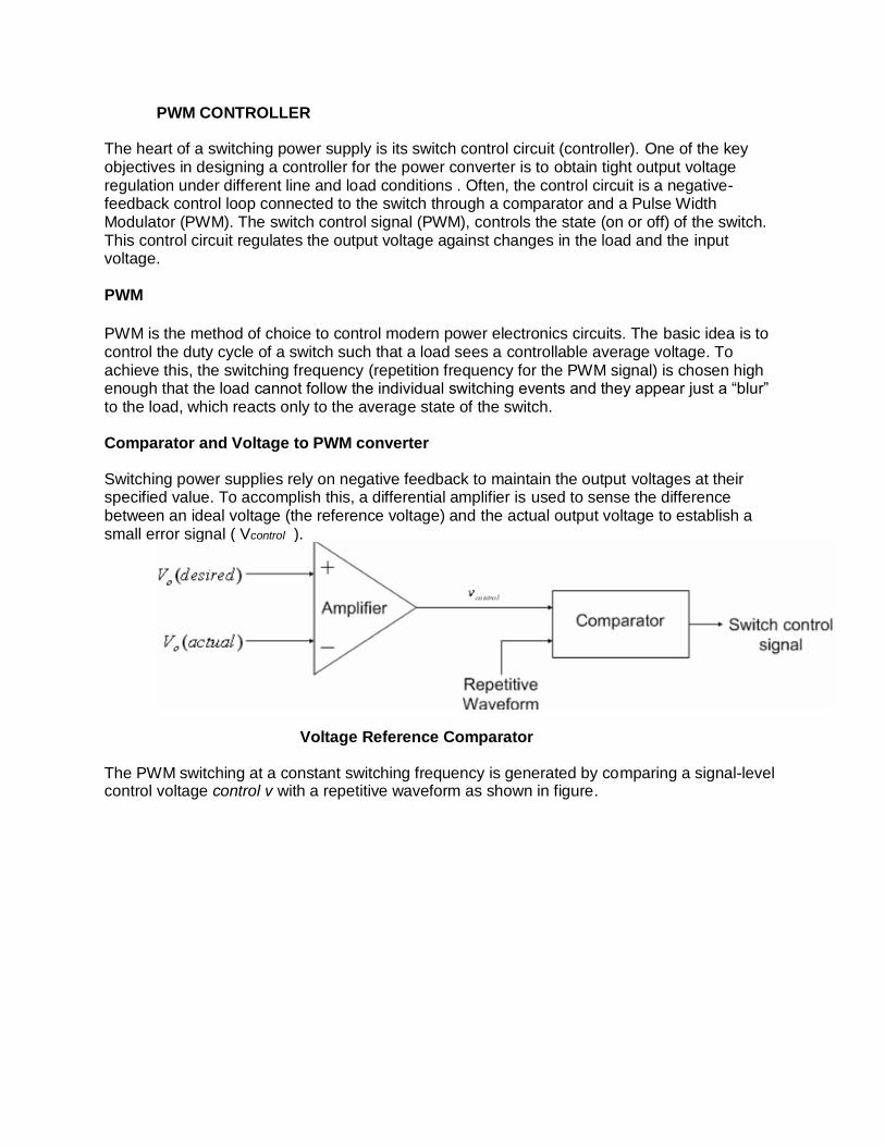
PWM CONTROLLER
The heart of a switching power supply is its switch control circuit (controller). One of the key objectives in designing a controller for the power converter is to obtain tight output voltage regulation under different line and load conditions . Often, the control circuit is a negative-feedback control loop connected to the switch through a comparator and a Pulse Width Modulator (PWM). The switch control signal (PWM), controls the state (on or off) of the switch. This control circuit regulates the output voltage against changes in the load and the input voltage. PWM
PWM is the method of choice to control modern power electronics circuits. The basic idea is to control the duty cycle of a switch such that a load sees a controllable average voltage. To achieve this, the switching frequency (repetition frequency for the PWM signal) is chosen high enough that the load cannot follow the individual switching events and they appear just a “blur” to the load, which reacts only to the average state of the switch. Comparator and Voltage to PWM converter
Switching power supplies rely on negative feedback to maintain the output voltages at their specified value. To accomplish this, a differential amplifier is used to sense the difference between an ideal voltage (the reference voltage) and the actual output voltage to establish a small error signal ( Vcontrol ).
Voltage Reference Comparator
The PWM switching at a constant switching frequency is generated by comparing a signal-level control voltage control v with a repetitive waveform as shown in figure.

PWM Comparator Signals
The frequency of the repetitive waveform with a constant peak, which is shown to be a sawtooth, establishes the switching frequency. This frequency is kept constant in a PWM control and is chosen to be in a few hundred kilohertz range.When the amplified error signal, which varies very slowly with time relative to the switching frequency, is greater than the sawtooth waveform, the switch control signal becomes HIGH, causing the switch to turn on.
Feedback Control System
The output voltages of dc power supplies are regulated to be within a specified tolerance band (e.g., ±1% around its nominal value) in response to changes in the output load and the input voltage lines. This process is accomplished by employing a negative feedback system which can be seen in figure.
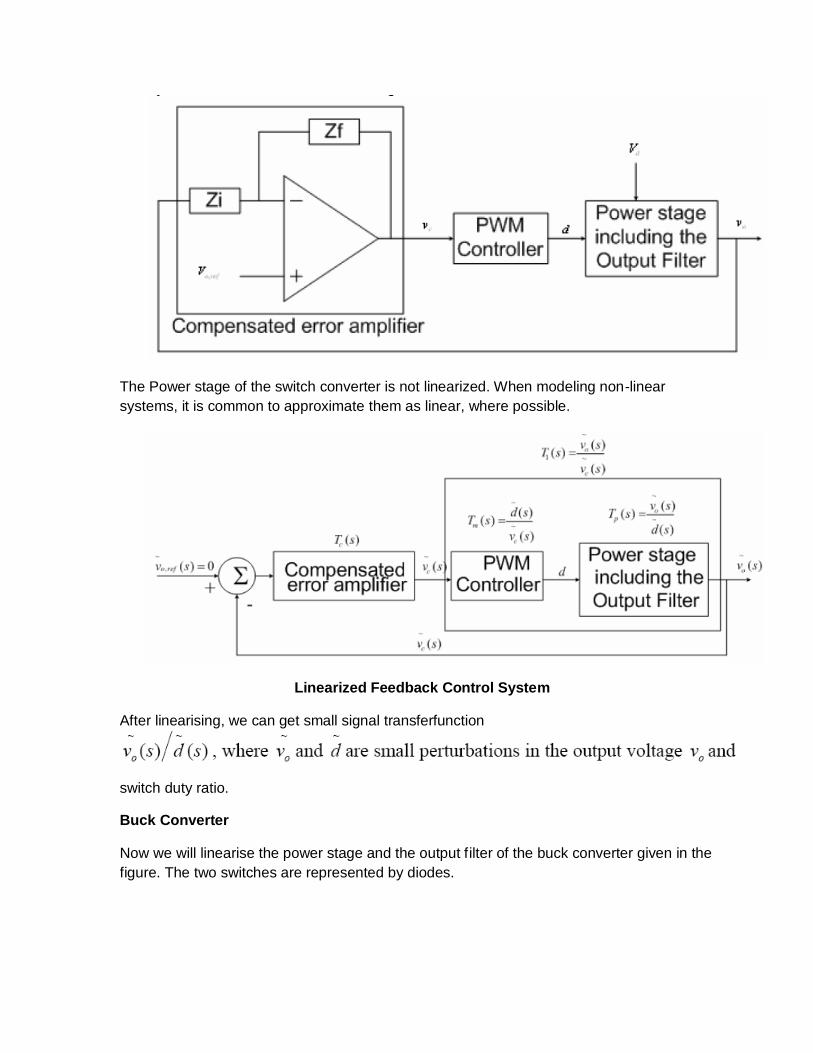
The Power stage of the switch converter is not linearized. When modeling non-linear
systems, it is common to approximate them as linear, where possible.
Linearized Feedback Control System
After linearising, we can get small signal transferfunction
switch duty ratio.
Buck Converter
Now we will linearise the power stage and the output filter of the buck converter given in the
figure. The two switches are represented by diodes.

rL is the inductor resistance, rC is the equivalent series resistance of the capacitance, and R is
the load resistance.
Where a zero is introduced due to the equivalent series resistance of the output capacitor at
the frequency

Pulse Width Modulator
In the direct duty ratio pulse-width modulator, the control voltage vc (t) , which is the output of the error amplifier, is compared with a repetitive waveform vr (t) , which establishes the switching frequency fs ,as shown in the figure . The control voltage vc (t) consists of a dc
component and a small ac perturbation component
The transfer function of Modulator is given by:
Compensator

After the values for external filter components are chosen (according to our requirements) than only the power stage is complete. The original filter of the buck converter by itself has a very low phase margin which needs to be increased. A better phase margin can be included by adding a suitable controller in a closed loop configuration. Proper compensation of the system will allow for a predictable bandwidth with unconditional stability. In most cases, a Type II or Type III compensated network will properly compensate the system. The ideal Bode plot for the compensated system would be a gain that rolls off at a slope of -20dB/decade, crossing 0db at the desired bandwidth and a phase margin greater than 45° for all frequencies below the 0dB crossing. Type III Compensation
Type III network shapes the profile of the gain with respect to frequency, but utilizes two zeroes to give a phase boost of 180°. This boost is necessary to counteract the effects of an under damped resonance of the output filter at the double pole. The Type III compensation circuit has two poles, with two zeros and a pole at its origin providing an integration function for better DC accuracy. Optimal selection of the compensation circuit depends on the power-stage frequency response.
After solving above circuit, we get:-

Voltage/Current Mode Control
The perceived advantage of CMC is feedback loop response; today’s high-frequency VMC
controlled converters closely rival their CMC counterparts. Most feedback controllers closely
rival their CMC counterparts. Most feedback controllers in buck converters use both the PWM
voltage and current mode controllers to produce a better steady-state response and to reduce
the voltage overshoots during start-ups.
Voltage Mode Control
This is a classical control & simple method in which there is only one feedback from the output voltage. PWM voltage mode controllers have disadvantages. Since the input voltage is a significant parameter in the loop gain, any changes in the input voltage will alter the gain and will change the dynamics of the system. The central issue is that a voltage mode controller alone cannot correct any disturbances or changes until they are detected at the output. In the voltagebased controllers the compensation loop is difficult to implement. Current Mode Control
In a current-mode control, an additional inner control loop is used as shown in figure, where the control voltage directly controls the output inductor current that feeds the output stage and thus the output voltage. Ideally, the control voltage should act to
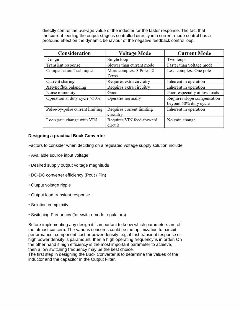
directly control the average value of the inductor for the faster response. The fact that
the current feeding the output stage is controlled directly in a current-mode control has a profound effect on the dynamic behaviour of the negative feedback control loop.
Designing a practical Buck Converter
Factors to consider when deciding on a regulated voltage supply solution include: • Available source input voltage • Desired supply output voltage magnitude • DC-DC converter efficiency (Pout / Pin) • Output voltage ripple • Output load transient response • Solution complexity • Switching Frequency (for switch-mode regulators) Before implementing any design it is important to know which parameters are of the utmost concern. The various concerns could be the optimization for circuit performance, component cost or power density. e.g. if fast transient response or high power density is paramount, then a high operating frequency is in order. On the other hand if high efficiency is the most important parameter to achieve, then a low switching frequency may be the best choice. The first step in designing the Buck Converter is to determine the values of the inductor and the capacitor in the Output Filter.

Table: Buck Converter Specifications
The applications for which these specifications could be useful for mobile phones (amongst other applications) where there is a continuous demand for progressively lower-voltage supplies. Design Equations
The power rating for the load to be driven is 200 mW. So according to this rating the value of load resistance should be 5 Ω. To ensure reliable operation, inductor must at least be 20% greater than its minimum value and the voltage ripple should be within 1%. Input Parameters For fsw = 100 KHz, ESR = DCR = 1. The reason for selecting these values was because for
these values the specifications which are mentioned were met. Using the MATLAB code we calculate the values of the different components. Buck Converter Circuit Transistors T1 & T2 are sized as 12μ & 6μ respectively and form the driver. T3 is the power switch sized at 1200μ and the low side NFET is 600μ. The large sizing of the transistor has
been optimized so as to reduce the resistance and hence the power lost in the switching.

Calculating Parameters
The values of the capacitor and inductor will vary. The values that have been calculated are for an ideal case, but they do provide us some rough values to start the designing and analysis of our Buck Converter.
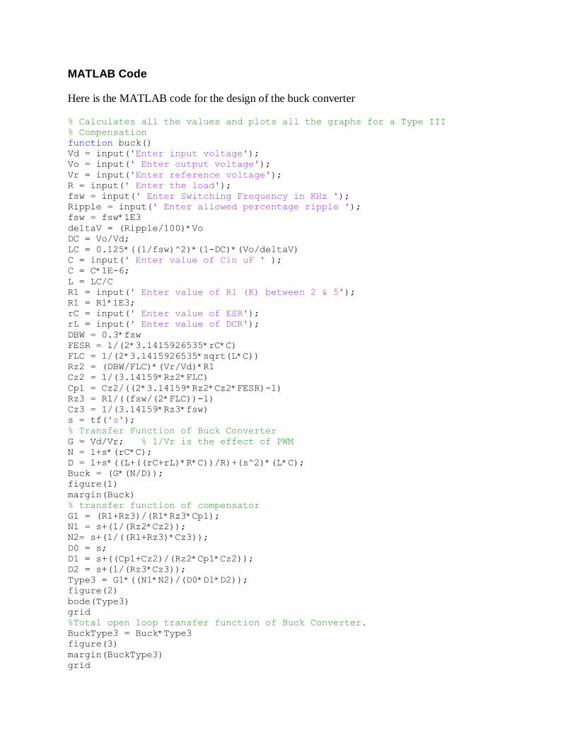
MATLAB Code
Here is the MATLAB code for the design of the buck converter
% Calculates all the values and plots all the graphs for a Type III % Compensation function buck() Vd = input('Enter input voltage'); Vo = input(' Enter output voltage'); Vr = input('Enter reference voltage'); R = input(' Enter the load'); fsw = input(' Enter Switching Frequency in KHz '); Ripple = input(' Enter allowed percentage ripple '); fsw = fsw*1E3 deltaV = (Ripple/100)*Vo DC = Vo/Vd; LC = 0.125*((1/fsw)^2)*(1-DC)*(Vo/deltaV) C = input(' Enter value of Cin uF ' ); C = C*1E-6; L = LC/C R1 = input(' Enter value of R1 (K) between 2 & 5'); R1 = R1*1E3; rC = input(' Enter value of ESR'); rL = input(' Enter value of DCR'); DBW = 0.3*fsw FESR = 1/(2*3.1415926535*rC*C) FLC = 1/(2*3.1415926535*sqrt(L*C)) Rz2 = (DBW/FLC)*(Vr/Vd)*R1 Cz2 = 1/(3.14159*Rz2*FLC) Cp1 = Cz2/((2*3.14159*Rz2*Cz2*FESR)-1) Rz3 = R1/((fsw/(2*FLC))-1) Cz3 = 1/(3.14159*Rz3*fsw) s = tf('s'); % Transfer Function of Buck Converter G = Vd/Vr; % 1/Vr is the effect of PWM N = 1+s*(rC*C); D = 1+s*((L+((rC+rL)*R*C))/R)+(s^2)*(L*C); Buck = (G*(N/D)); figure(1) margin(Buck) % transfer function of compensator G1 = (R1+Rz3)/(R1*Rz3*Cp1); N1 = s+(1/(Rz2*Cz2)); N2= s+(1/((R1+Rz3)*Cz3)); D0 = s; D1 = s+((Cp1+Cz2)/(Rz2*Cp1*Cz2)); D2 = s+(1/(Rz3*Cz3)); Type3 = G1*((N1*N2)/(D0*D1*D2)); figure(2) bode(Type3) grid %Total open loop transfer function of Buck Converter. BuckType3 = Buck*Type3 figure(3) margin(BuckType3) grid

Output
Enter input voltage1.55
Enter output voltage1
Enter reference voltage1
Enter the load.2
Enter Switching Frequency in KHz 100
Enter allowed percentage ripple 1
fsw =
100000
deltaV =
0.0100
LC =
4.4355e-010
Enter value of Cin uF 5
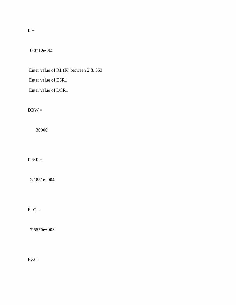
L =
8.8710e-005
Enter value of R1 (K) between 2 & 560
Enter value of ESR1
Enter value of DCR1
DBW =
30000
FESR =
3.1831e+004
FLC =
7.5570e+003
Rz2 =
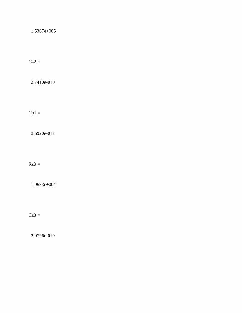
1.5367e+005
Cz2 =
2.7410e-010
Cp1 =
3.6920e-011
Rz3 =
1.0683e+004
Cz3 =
2.9796e-010

Transfer function:
23.15 s^3 + 6.278e006 s^2 + 3.558e011 s + 5.219e015
------------------------------------------------------------------------
4.435e-010 s^5 + 0.0006816 s^4 + 262.1 s^3 + 2.901e007 s^2 + 6.283e010 s
Graphs
Figure 1 : Bode plot of Buck Converter

Figure2 : Bode plot of type III Compensation Network

Figure 3: Bode plot of Total Loop Buck Converter
Verilog Code Generation And Simulation
Matlab code was modified by converting transfer functions of compensator and power
stage including output filter from S-domain to Z-domain by Bilinear transformation and
writing it in difference equation form to run the code in simulink HDL coder. Then the
modified Matlab code was loaded to generate Verilog HDL in simulink HDL coder.
Verilog Code
‘timescale 1ns/1ns
module buck (clk,reset,clk_enable);
input clk;
input reset;
input clk_enable;
wire enb;
real TmpGroundAtEmbedded_MATLAB_FunctionInport6_out1; //double

real TmpGroundAtEmbedded_MATLAB_FunctionInport5_out1; //double
real TmpGroundAtEmbedded_MATLAB_FunctionInport4_out1; //double
real TmpGroundAtEmbedded_MATLAB_FunctionInport3_out1; //double
real TmpGroundAtEmbedded_MATLAB_FunctionInport2_out1; //double
real Constant_out1; //double
wire [63:0] s; //ufix64
wire [63:0] s_1; //ufix64
wire [63:0] s_2; //ufix64
wire [63:0] s_3; //ufix64
wire [63:0] s_4; //ufix64
wire [63:0] s_5; //ufix64
wire [63:0] s_6; //ufix64
real Embedded_MATLAB_Function_out1; //double
initial
begin
TmpGroundAtEmbedded_MATLAB_FunctionInport6_out1=0.0000000000000000E+000;
end
initial
begin
TmpGroundAtEmbedded_MATLAB_FunctionInport5_out1=0.0000000000000000E+000;
end
initial
begin
TmpGroundAtEmbedded_MATLAB_FunctionInport4_out1=0.0000000000000000E+000;
end

initial
begin
TmpGroundAtEmbedded_MATLAB_FunctionInport3_out1=0.0000000000000000E+000;
end
initial
begin
TmpGroundAtEmbedded_MATLAB_FunctionInport2_out1=0.0000000000000000E+000;
end
initial
begin
Constant_out1 =1.0000000000000000E+000
end
assign s=$realtobits(Constant_out1);
assign s_1=$realtobits(TmpGroundAtEmbedded_MATLAB_FunctionInport2_out1);
assign s_2=$realtobits(TmpGroundAtEmbedded_MATLAB_FunctionInport3_out1);
assign s_3=$realtobits(TmpGroundAtEmbedded_MATLAB_FunctionInport4_out1);
assign s_4=$realtobits(TmpGroundAtEmbedded_MATLAB_FunctionInport5_out1);
assign s_5=$realtobits(TmpGroundAtEmbedded_MATLAB_FunctionInport6_out1);
Embedded_MATLAB_Function Embedded_MATLAB_Function (clk.(clk),.clk_enable),.reset(reset)
.fsw(s),.Ripple(s_1),.C(s_2),.R1(s_3),rC(s_4),.rL(s_5),.Vo(s_6)
always@*Embedded_MATLAB_Function_out1<=$bitstoreal(s_6);
endmodule
module Embedded_MATLAB_Function (clk,clk_enable,reset,fsw,Ripple,C.R1,rC,rL,Vo);
input clk;
input reset;

input clk_enable;
input [63:0] fsw;
input [63:0] Ripple;
input [63:0] C;
input [63:0] R1;
input [63:0] rC;
input [63:0] rL;
output [63:0] Vo;
reg [63:0] Vo;
initial
Vo=$realtobits(0.0);
initial
begin
Vo=$realtobits(1.0);
end
endmodule
Future Work
Most of the simulations have been done using ideal components or modelled in Verilog code. It
would be a good challenge to include the transistor level modelling there and see the responses
of the overall system. Eventually the layout for a fully testable and working DC-DC Converter
could be done in 90nm process. Extensive study was not made into the reduction of the
overshoot that is observed in the output and main emphasis remained on the ripple during
steady state.
Conclusion
This project has given a basic insight in to the working of a buck converter that could be
considered to be manufactured on-chip. Though a few of the issues have not been solved but
they have been highlighted as potential areas in which more refinements are required. The
effect of the system when RL switches from one value to another have also been observed.
Though we have considered the ideal cases only but if all non-ideality would be considered than
we would see that ripple would increase and the efficiency would also decrease. We have

generated the Verilog HDL code and simulated in SILOS Verilog HDL Simulator which can be
further implemented on Field Programmable Gate Arrays (FPGA) to observe the output.
References
Books
[1] Ned Mohan, Tore M. Undeland, William P. Robbins, “Power Electronics: Converters,
Applications, and Design”, 3rd Edition, Wiley.
[2] B. J. Baliga, “Modern Power Devices”, New York: Wiley, 1987.
Papers
[1] Jinwen Xiao, Angel Peterchev, Jianhui, Seth Sanders, “An Ultra-Low-Power Digitally-
Controlled Buck Converter IC for Cellular Phone Applications”, Applied Power Electronics
Conference and Exposition, 2004. Nineteenth Annual IEEE, Volume 1, Issue, 2004 Page(s):
383 - 391 Vol.1
[2] Michael D. Mulligan, Bill Broach, and Thomas H. Lee, “A Constant- Frequency Method for
Improving Light-Load Efficiency in Synchronous Buck Converters”, Power Electronics Letters,
IEEE Volume 3, Issue 1, March 2005