photonic integrated circuit design in a foundry+fabless
TRANSCRIPT

IEEE JOURNAL OF SELECTED TOPICS IN QUANTUM ELECTRONICS, VOL. 25, NO. 5, SEPTEMBER/OCTOBER 2019 8201014
Photonic Integrated Circuit Design in aFoundry+Fabless Ecosystem
Muhammad Umar Khan , Member, IEEE, Yufei Xing, Yinghao Ye , and Wim Bogaerts , Senior Member, IEEE
(Invited Paper)
Abstract—A foundry-based photonic ecosystem is expected tobecome necessary with increasing demand and adoption of photon-ics for commercial products. To make foundry-enabled photonicsa real success, the photonic circuit design flow should adopt knownconcepts from analog and mixed signal electronics. Based on thesimilarities and differences between the existing photonic and thestandardized electronics design flow, we project the needs and evo-lution of the photonic design flow, such as schematic driven design,accurate behavioral models, and yield prediction in the presence offabrication variability.
Index Terms—CMOS, photonic integrated circuits(PICs),foundry, fabless design, photonics ecosystem, process design kit(PDK), circuit design, design flow.
I. INTRODUCTION
PHOTONICS has made tremendous progress in the last fewyears. The application base has broadened to a range of
applications from optical communications to sensing. The pho-tonics market today is shared by several material systems suchas group IV semiconductors (silicon and germanium) [1], [2],compound III-V semiconductors (indium phosphide and gal-lium arsenide) [3], [4], silica planar lightwave circuits (PLC)[5], silicon nitride (with flavors such as TriPlex) [6], differentpolymers [7], and more exotic materials [8]. Among these, groupIV semiconductor based photonics, often called silicon photon-ics, has become a prominent technology for photonic integratedcircuits (PIC). This is due to the use of the existing comple-mentary metal oxide semiconductor (CMOS) infrastructure andthe high material index contrast between the guiding silicon andthe cladding which permit sub-micron waveguides and a highintegration density.
Silicon photonics itself covers a range of material systemssuch as silicon-on-insulator (SOI), silicon nitride-on-insulator
Manuscript received December 14, 2018; revised April 18, 2019; acceptedMay 18, 2019. Date of publication May 24, 2019; date of current version June20, 2019. This work was supported in part by the Flemish Research Foundation(FWO-Vlaanderen) under Grant G013815N, and in part by the Flemish Agencyfor Innovation and Entrepreneurship (VLAIO) with the MEPIC Project. (Cor-responding author: Muhammad Umar Khan.)
The authors are with the Ghent University—IMEC, Photonics ResearchGroup, Department of Information Technology, 9052 Ghent, Belgium, andalso with the Center for Nano and Biophotonics (NB-Photonics), 9052Ghent, Belgium (e-mail: [email protected]; [email protected]; [email protected]; [email protected]).
Color versions of one or more of the figures in this paper are available onlineat http://ieeexplore.ieee.org.
Digital Object Identifier 10.1109/JSTQE.2019.2918949
(SiN), germanium-on-silicon, germanium-on-silicon nitride andsilicon-on-silicon nitride. All these material systems are compat-ible with CMOS fabrication facilities and processes and supportdensely integrated circuits, so we can categorize all of them assilicon photonics. Among these silicon photonics material sys-tems, the SOI is by far the most mature and the most widelyused platform. It provides the highest possible integration den-sity with the highest potential for high-volume manufacturing.However, the manufacturing volumes for even the most usedSOI platform fall still several orders of magnitude short of thosein CMOS electronics. To give an idea, few tens of thousands ofwafers are required for entire photonics market per year whichis in contrast to many tens of thousands of wafers being pro-cessed by a typical CMOS electronics fab in only a month [9].Therefore, it is not feasible to set up a new infrastructure for suchsmall production volumes and makes it compelling to use theexisting CMOS fabrication facilities for silicon photonics. Thisavailability of an existing foundry distinguishes silicon photon-ics from PIC technologies in other material systems based onthe compound semiconductors, silica, and polymers.
A foundry provides fabrication services on one or more stan-dardized platforms that can be accessed by third-party (fabless)designers. The third party can access the fabrication services di-rectly or through a broker for multi project wafer (MPW), ded-icated engineering runs, or for low or high-volume production[10]. As SOI is the most popular platform, so several CMOSfoundries offer the open-access fabrication facilities for SOIplatform. Some of the prominent foundries providing prototyp-ing, MPW, and large scale production facilities are tabulatedbelow in Table I. A more detailed overview of foundry activi-ties, specific to silicon photonics, can also be found in [10].
To make a foundry model successful, offered technologyplatform should be sufficiently generic to address a diverseapplication market. Silicon nitride (SiN) being a CMOS compat-ible material was investigated to target life science applications(requiring visible light) because silicon is not transparent forwavelengths smaller than 1.1 µm. The transparency windowfor SiN extends to 0.4 µm which makes it very useful for lifescience applications [28]–[30]. The foundries providing thesilicon nitride fabrication facilities are tabulated in Table II. Amore detailed overview of foundry activities, specific to siliconnitride, can also be found in [31]. Integration of light sourcesand detectors makes SiN platform even more attractive forvarious applications [32]. Still, to make the foundry enabled
1077-260X © 2019 IEEE. Translations and content mining are permitted for academic research only. Personal use is also permitted, but republication/redistributionrequires IEEE permission. See http://www.ieee.org/publications_standards/publications/rights/index.html for more information.

8201014 IEEE JOURNAL OF SELECTED TOPICS IN QUANTUM ELECTRONICS, VOL. 25, NO. 5, SEPTEMBER/OCTOBER 2019
TABLE ISOME OF THE AVAILABLE OPEN-ACCESS SILICON-ON-INSULATOR FABRICATION FACILITIES
TABLE IISOME OF THE AVAILABLE OPEN-ACCESS SILICON NITRIDE FABRICATION
FACILITIES
photonics economically feasible for other material platforms,the margin on the fabrication needs to be sufficient to recoverthe investments and operations of the platform. This makesthe foundry model suitable either for markets with sufficientlyhigh volume (e.g., datacom transceivers) or for high-value,high-complexity products, which can often be found in medical,defense and aerospace markets. The added value of the PICtechnology now comes from the integration of very complexfunctionality on a chip, which requires a reliable design flow thatallows both the foundry and the third-party designers to makefirst-time-right designs.
Because the foundry model separates the designers from theactual technology, the design flow, software tools, and design kitsshould fill the gap that now separates the designers from physi-cal fabrication. Circuit design already requires a higher level ofabstraction, but the fact that in a foundry model the designer isnow physically shielded from the actual technology (literally: inmany cases the fabs do not disclose all the technological detailsof the fabrication to the users) requires some formal mechanismthat enables the designers to design a working circuit reliably.
So, it is crucial to the success of a real foundry model for pho-tonic integrated circuits to standardize the design flow for thephotonic circuits in a similar fashion as it was done for electron-ics. In this article, we provide an overview of the similarities anddifferences between the currently used design flow for photonicintegrated circuits, and especially larger-scale photonic circuits,to the standardized design flow for electronics. The best com-parison is drawn with analog electronics, not digital, as analogelectronics is still somewhat rooted in physical layout design as
electronics, and photonic functions today are still mostly ana-log. Based on the differences we project how the design flowfor the foundry enabled photonic integrated circuits will evolveand which requirements need to be fulfilled to make it a success,especially in the realm of standardization.
It can be said that the photonic integrated circuits using SOIare really moving towards electronics like circuits where thefunctionality is designed as a connection of functional buildingblocks instead of optimizing the component geometries. Thenumber of chips fabricated by electronics is enormous in com-parison to the photonic chips. So, in order to reduce the cost ofthe fabrication and to make the foundry enabled photonics thenumber of fabricated chips should scale up considerably. Thecapital expenditure for the foundries fabricating photonic chipsis pretty high due to the small number of volumes for the pho-tonic chips. So, either high margin chips with a lot of complexityor a foundry model to spread volumes over many applicationsare needed.
II. PHOTONICS DESIGN FLOW TODAY
Good design flow is a combination of different tasks organizedin a systematic and reproducible manner to achieve the ultimategoal of turning an idea into a working chip. The step in the designflow needs to be backed up by efficient software tools that takethe designer all the way to the tape-out of a working chip design,and this with high yield. Present photonics design flow can bedivided into four major parts i.e.� Component design & optimization� Circuit design & simulation� Layout generation� VerificationHere we briefly discuss each of these to find out the miss-
ing links in this designs flow. Detailed design flow is discussedin [36].
A. Component Design & Simulations
Even though the common term for photonic chips is pho-tonic integrated circuits (PIC), PIC design in the past couple

KHAN et al.: PHOTONIC INTEGRATED CIRCUIT DESIGN IN A FOUNDRY+FABLESS ECOSYSTEM 8201014
of decades has focused largely on the design of building blocks(also called devices or component). As the functionality of de-vices is entirely determined by the geometry and material pa-rameters, good device relies heavily on the simulation of lightpropagation using electromagnetic modeling techniques such asfinite difference time domain (FDTD) [37], eigenmode expan-sion (EME) [38], finite element (FE) [39], or beam-propagationmethod (BPM) [40].
We can separate devices in passive and active devices. Passivephotonic devices are pure optical and therefore have no electricalfunction. In a first approximation, their behavior is also linear,but the functionality of passive devices can also be extendedto optical nonlinearities. Passive devices range from elementarywaveguide-based geometries like directional couplers [41] tocomplex periodic geometries like photonic crystals [42]. In apassive device design, there is essentially unlimited freedom todesign the geometries, as long as it is compatible with the chosenfabrication technology. Optimization of the devices with such alarge degree of freedom can be challenging and requires special-ized algorithms [43]–[47], but this can often lead to impressivefunctional performance on a tiny footprint.
Active components also include an electrical function. Thiscan be a tuning of a passive device through thermal and elec-tromechanical effects. Other active devices include electro-optic conversions such as lasers, modulators, and amplifiers,or optoelectric conversion in photodetectors. Modeling such de-vices usually involves the physics of multiple domains (ther-mal, mechanical, carrier dynamics) and requires multiphysicssimulations.
Given that the geometry entirely determines the propagationof light, photonic devices on a chip will be sensitive to varia-tions in geometrical parameters and environment. This sensitiv-ity depends very much on the material system, and especially therefractive index contrast between the materials used for wave-guide cores and the materials used for the surrounding cladding.Higher index contrast allows for tighter confinement of light, butthis will also make the device more sensitive to variations. Thisis particularly prominent in silicon photonics with its submicronwaveguides and huge index contrast between the guiding layerand the claddings.
B. Circuit Design & Simulations
In contrast with device design, circuit design does not re-volve around geometries. Instead, the focus is on connectingknown devices in such a way that some desired, higher level offunctionality is achieved. The geometric layout is of secondaryimportance and relates more to the placement of building blocksthan adjusting their geometries. Currently, the complexity of thephotonic integrated circuits is generally low, with tens to hun-dreds of components in a single circuit. This is a somewhat ar-bitrary metric, as the component count is not standardized (e.g.,sometimes individual waveguide bends are counted as a sepa-rate component), and even the most complex designed circuits,such as multi-channel transceivers [48] and optical phased ar-rays [49], are a parallelization of simpler circuits. The circuit
size is gradually improving (increasing) with improved technol-ogy platforms, especially for Indium Phosphide PICs [50]–[52]and silicon photonics [10], [53]–[55].
An increase in complexity depends very much on the avail-ability of a circuit design flow and software tools that help thedesigner scale up his circuit design in a reliable way. This iswhere circuit design today is in full evolution. In order to predictthe behavior of a circuit, the design needs to be simulated. Un-like with devices, it is no longer possible to use computationallyintensive electromagnetic simulations to calculate the responseof an entire circuit. Instead, in circuit simulation, the individualdevices are abstracted into a behavioral response which mapsthe inputs to the outputs. These behavioral responses (compactmodels) are constructed based on physical simulations, theory,and measurements. There are several circuit simulation toolsavailable in the market [56]–[60], and their use is increasing.However, the usefulness of these circuit simulation tools todayis not limited by their engine and algorithms, but by the qualityand availability of the compact models for the building blocksoffered by the technology platforms. The circuit simulation canonly be as accurate as the behavioral models of the components.
Photonic circuit simulations can be broadly divided into twocategories, i.e. frequency domain and time domain simulations.Frequency domain simulations of the circuit calculate the wave-length dependent response (both amplitude and phase) betweenthe input and the output ports of the circuit. As photonic com-ponents are wavelength dependent, the used behavioral modelsneed to be accurate for the entire simulated frequency range.Frequency-domain simulations are most useful for passive lin-ear photonic devices. These can be described by a frequency-dependent scatter matrix (S-matrix). As a linear system supportssuperposition, a scatter matrix describes all possible linear re-sponses of the circuit. Also, as the S-matrix formalism is wellknown from microwave design, there exist standardized formats(e.g., Touchstone) to exchange S-matrix data [61]. Beyond lin-earity, the frequency-domain formalism can also be useful todescribe certain nonlinearities, or the transmission of passivedevices which are actively tuned, with a tuning that is muchslower than the optical phenomena. Usually, this requires someiterative strategy to converge to the eventual frequency response.
Time domain simulations, on the other hand, solve the re-sponse of the circuit for a time-variant stimulus on the inputports of the circuit. The response of the circuit is solved bytime-stepping the signals between all the nodes in the circuit,and updating the models at each step. The individual modelsshould capture the underlying physics, either by incorporatingthe governing equations or by approximating them using a fittedblack-box modeling strategy. Unlike S-matrices, there is littleor no standardization in time domain circuit models for pho-tonics. The models can be implemented in a variety of toolsand languages, and their implementation can range from a setof ordinary differential equations (ODE) to fully-custom codemodels.
One particular implementation is a state-space model, wherethe behavior of a component is described using a set of states,which are related with one another and the input signals througha set of ordinary differential equations [62], [63]. For each time

8201014 IEEE JOURNAL OF SELECTED TOPICS IN QUANTUM ELECTRONICS, VOL. 25, NO. 5, SEPTEMBER/OCTOBER 2019
step, first the states are updated based on the incoming signals,and then the outgoing signals are updated based on the newstates. The variables in a state-space model can represent actualphysical variables (e.g., the temperature of a thermo-optic phaseshifter), or they can be fitted to some measured or simulated re-sponse curve, resulting in a black-box model that mimics thebehavior of the component but where the internal variables haveno relation with the actual physics. For instance, time domainmodels for the passive linear optical components can be fittedfrom frequency response by deriving a corresponding linear fil-ter model, either with a finite impulse response (FIR) or infiniteimpulse response (IIR) [64], [65]. Note that time domain mod-els usually work in a limited bandwidth, and model the signalas a modulation on top of a carrier wavelength. This works wellfor modeling simple communication systems, and it can be ex-panded to multiple carrier wavelengths for modeling wavelengthdivision multiplexing (WDM) circuits, but it will not scale to thefull optical bandwidth of tens of THz, as this would require ei-ther very short time steps or a massive amount of data exchangebetween components [36].
C. Process Design Kits (PDK)
An essential requirement for efficient circuit design is a libraryof qualified building blocks from which to construct a circuit.These building blocks are the result of the component designprocess. Historically, photonic component design and circuit de-sign were combined in the same person or group, but with theemergence of foundry-based fabrication, a new communicationchannel is needed.
The process design kits (PDK) is the bridge between thefoundry and component designers on the one hand, and the cir-cuit designers on the other, and it has become an essential as-pect of today’s PIC manufacturing ecosystem. A PDK containsa library of the optimized components for a particular platformalong with other practical details like design requirements, basicbuilding blocks, verification deck, etc. It allows a circuit designer(with the right set of software tools) to construct a circuit thatcan be fabricated by the foundry.
The foundries usually maintain the PDKs for their technol-ogy platforms, but it is not uncommon that foundry customersextend the vanilla PDK with their proprietary component andsubcircuit designs. The initial PDKs from photonic foundrieswere limited to information about the fabrication process, some-times accompanied by a set of layouts of building blocks. Theaddition of parametric cells (PCells) for essential componentssuch as waveguides came next, along with design rule checking(DRC) decks. Today, we see the emergence of PDKs with devicemodels capturing the nominal (ideal) behavior of the devices inthe building block libraries.
In a foundry-enabled fabless ecosystem, the process develop-ment kit (PDK) is playing an increasingly important role, as itserves as the middle man between the designer and the foundry,as shown in Fig. 1. The richness of the component library, thesupported software tools and the sophistication of the devicemodels have become a differentiator that is as important as thequality of the fabrication technology. This is understandable: as
Fig. 1. The process development kit provides the necessary information aboutthe fab to the designer. At present, process information, design requirements,basic building blocks, compact models and the verification decks are usuallyavailable in a PDK.
in electronics, the functionality of circuits is not necessarily de-termined by the quality of the single transistor, but by the circuit,and the reliability of the circuit design libraries determines thecomplexity of circuits that can be designed.
PDKs also allow fabs to encapsulate the essential propertiesof their technology platform without having to reveal the in-timate details, which they might consider valuable intellectualproperty or trade secrets. Library building blocks can be repre-sented as black boxes, and behavioral models can be compiled,so the actual equations and parameters are no longer accessi-ble to the circuit designer. However, this encapsulation comesat a price: it requires some commitment of the fab to guaranteethe performance of these black-box components, as the designercannot second-guess the implementation and could, therefore,hold the fab liable in case their library components do not workaccording to the original specs.
D. Circuit Layout Generation
When sending design for fabrication in a foundry, it is com-municated as a layout for the different mask layers. The lay-out is exchanged using graphic data system (GDSII) or openartwork system interchange standard (OASIS) format. GDSIIhas been the industrial standard for over 30 years, but recentlyOASIS seems to be gaining some traction because of smallerfile sizes. Unlike in component design, where the layout con-sists of custom geometries, the layout in a circuit design mostlyconsists of placement of (parametric) cells, connected by op-tical waveguides and/or electrical wiring. Optical connectionsof components are more complicated than electrical connec-tions. Waveguides need to maintain a minimum bend radiusand separation to prevent excess waveguide losses and parasiticcoupling. Most waveguide routing today is done manually, al-though some software tools support waveguide generation withdifferent curve algorithms [66], [67]. Fully automatic routing of

KHAN et al.: PHOTONIC INTEGRATED CIRCUIT DESIGN IN A FOUNDRY+FABLESS ECOSYSTEM 8201014
complex layouts with tens of waveguides is not yet available.One particular obstacle for this is that most PIC technologiesonly support a single waveguide layer, and therefore need to in-troduce engineered waveguide crossings to connect nontrivialcircuit topologies. [68], [69].
E. Verification
Once the layout has been generated, the layout is checked forpotential errors and violations of the design rules provided by thefab. The design rules from the fab usually include the minimalcritical dimensions, sharp angles and pattern density require-ments. For this, photonics design relies on Design rule check-ing (DRC) software tools from the electronics, such as Calibreby Mentor [70], Cadence’s Physical Verification System [71]or Synopsis IC Validator [72]. The foundries usually provide adesign rule checking deck for one or more of these tools andrequire that the designers submit a DRC-clean design. One ofthe problems with early DRC decks for photonics arose fromthe fact that DRC software for electronics was not designed tohandle the smooth curvilinear shapes that are typical for opticalon-chip waveguides, and sometimes generate false errors. How-ever, new DRC rules for the curvilinear structures and all-anglepolygons are helping to improve the automated DRC checkingprocess [73].
F. Summary of the Present Design Flow
Even when using standard building blocks from PDKs, pho-tonic circuits today are still mainly designed as a physical lay-out. The design process does not have a smooth translation fromthe functional idea to the physical layout over a more abstractschematic, as is the typical workflow in analog electronics de-sign. This lack of flow in this process is making it hard fordesigners to scale up the functionality and complexity of theirphotonic circuits.
III. PHOTONIC VERSUS ELECTRONIC DESIGN FLOW
It is essential for the success of a real foundry based modelfor photonic integrated circuits to standardize the design flowsimilarly as it was done for electronics. In this section, we listthe shortcoming in the current photonics design flow presentedin the previous section. These shortcomings are marked downbased on a comparison to the electronics design flow.
A. Compact Models
It has been mentioned in the previous sections that PDKsplay an important role in a foundry enabled fab-less ecosystemas they provide the required information about the fab to thedesigner. The compact models, parametric cells and sensitivityof the performance parameters to fabrication variability are themost important elements of a PDK for the designer. Accuratecompact models of the components are required for reliable cir-cuit simulations, and the accuracy and standardization of com-pact models have played an important role in the success of afab-less ecosystem for electronics. Photonic PDKs on the otherhand lack in terms of the maturity and accuracy of the compact
models. There is no standardization regarding the building ofthe compact models, so even the available compact models arespecific to particular simulation software tools. So, standardiza-tion is required to expand the adoption and usability of compactmodels. In analog electronics design, such standardization hasled to the widespread adoption of SPICE and Verilog-A, whichin turn have stimulated fabs to invest in good model generation.As a result, electronic designers can trust their simulations, evenfor rather aggressive circuit designs.
Model standardization can also be done on the level of devices,by agreeing on a set of standard device descriptions for manyconventional devices. This could start with passive devices suchas waveguides, directional couplers, splitters, etc., but it couldwell be extended to include modulators and detectors. Amplifiersand lasers are examples of optical devices for which a set ofwidely accepted standard models have been developed [74].
B. Standardized Design Flow
Most of the electronic designers follow a standardized work-flow with circuit hierarchy and reusable parametric cells. Ontop of the standardized work-flow, modern electronic designautomation (EDA) tools help them automate the tasks whichenable them to achieve the first-time-right design for even verycomplex circuits. Currently, there is no standardized design flowfor the photonics, but with the increasing complexity of the pho-tonic integrated circuits, the design process is evolving towardsthe standardization of the workflow in line with the electronicdesign automation.
As we will discuss in Section IV, this involves a moreschematic-based approach to capture an idea into a circuit rep-resentation, before drilling down to the details of the circuit lay-out. In electronics, this translation is increasingly supported bysoftware automation, where the layout tool can provide place-ment guidance and visual feedback on connectivity through flylines, helping the designer to avoid connectivity mistakes. Thisschematic driven design speeds up the physical layout dramati-cally and is also emerging for photonics [66], [75].
C. Verification
The generated layout from the schematic is verified before for-warding to the foundry. However, electronic circuits are verifiedat a much deeper level than just checking the design rules. Themore critical verification step involves checking of the function-ality of the generated layout actually matches the original cir-cuit design intent; this step is called the layout versus schematic(LVS) verification. LVS identifies the connectivity of the cir-cuit by checking the overlaps of all electrical wiring. On top ofthat, more sophisticated LVS checkers also analyze the geometryof the wires and extract capacitive and inductive parasitic cou-pling. From this parasitic extraction, a more complicated circuitschematic is generated that can be simulated and compared tothe original simulations.
In photonics, DRC has become a common practice, but LVSchecking has proven to be complicated. First of all, it is not easyto extract the connectivity of photonic components from the lay-out. The primary connections can be fairly easily identified, as

8201014 IEEE JOURNAL OF SELECTED TOPICS IN QUANTUM ELECTRONICS, VOL. 25, NO. 5, SEPTEMBER/OCTOBER 2019
Fig. 2. (a) A waveguide is extended using another waveguide of the samedimensions. The waveguides need to be accurately aligned to get rid of theback-reflections and scattering. (b) Two waveguides do not come in physi-cal contact with each other but light couples from one waveguide to another.(c) Two waveguides physically touch each other in a waveguide crossing, butone mode does not interrupt the other.
Fig. 3. The parasitics due to the back reflections/scattering in a straight wave-guide and due to coupling in closely packed waveguides are depicted.
the waveguide ports of the building blocks and subcircuits canbe annotated, and these connections can be checked against theoriginal schematic. But it is much harder to identify uninten-tional connections and parasitics.
This can be explained using the example of the simplest pho-tonic component, i.e., waveguide. Three different scenarios ofwaveguide connectivity are shown in Fig. 2 below. In the firstscenario, a waveguide is connected to another waveguide of thesame type. When the position and orientation match perfectly,they are properly connected. There should be no offset betweenthe waveguides; otherwise, back-reflections and scattering willinduce parasitic effects, Fig. 3. In a directional coupler, twowaveguides are not physically in contact with each other butlight can still couple from one waveguide to another. If such adirectional coupler is implemented as a device, then it can be rec-ognized for its function. But if such a coupler is unintentionallyimplemented by bringing two waveguides too close together, the
parasitic coupling will occur, and the devices become connectedwhen they should not be. This connectivity is not so trivial todetect and quantify in a layout. On top of that, such parasiticcoupling is wavelength and geometry dependent as the couplingstrength changes with the gap, coupling length and wavelengthof operation. It should be mentioned here that this problem isnot unique to photonics, for RF there is a similar challenge inverification, where usually designer expertise is complementedwith full-scale electromagnetic simulation (which is still possi-ble on an RF circuit, but not on a photonics circuit, as the circuitscale is much larger compared to the waveguide). A waveguidecrossing is another example where an intentional design suggestscoupling, but where it is engineered to let light pass straight on.On top of that, extracting parasitic back-reflections and scatter-ing in waveguides, which can be stochastic in nature is very hard,but these effects can have a significant detrimental effect on theperformance of larger circuits.
So, as it stands today, photonic layouts are not that easilyverified with the original schematics. One thing that is now be-coming more common is that at least the layout parameters ofthe building blocks are being taken back into the circuit simula-tion. For instance, the actual waveguide length can play a vitalrole in balancing interferometric circuits, so post-layout circuitsimulations has proven a big step forward in photonic circuitdesign [66], [76]. Sometimes, electromagnetic simulations arerequired to find out the connectivity from a photonic layout,which is prohibitively expensive in terms of simulation time.
D. Variability Analysis
Variability analysis and the yield prediction are an essentialpart of the standardized electronics design flow. Traditionally,this was done through corner analysis, where the circuit is calcu-lated using the best (fast) and the worst (slow) case scenarios forboth PMOS and NMOS transistors. Based on this analysis, a cir-cuit could be designed to work even in the worst-case scenario.More recently, corner analysis is gradually being supplementedto more complex statistical approaches, as reliance on corneranalysis alone would usually result in overly conservative de-signs. With such statistical methods, yield can be predicted fordifferent variations of a designed electronic circuit in the pres-ence of a variety of different fabrication parameters.
In photonics corner analysis is not directly applicable, butMonte-Carlo simulations for variability analysis and yield pre-diction are needed, and slowly finding their way in the designflow [77], [78]. Variability for photonics can be explained withthe example of the most basic building blocks, i.e., waveguide. Asilicon wire waveguide is very sensitive to change in linewidthand thickness. Therefore, the effective and the group indiceschange as the geometry of the waveguide changes. This changein propagation constants can lead to phase errors in interfero-metric circuits with multiple delay lines, even when waveguidesare placed close together. This sensitivity depends very much onthe choice of technology platform, and especially the refractiveindex contrast between core and cladding. In silicon, a smallvariation in the waveguide core dimensions (linewidth, thick-ness) on the order of 1 nm can lead to shifting in wavelength

KHAN et al.: PHOTONIC INTEGRATED CIRCUIT DESIGN IN A FOUNDRY+FABLESS ECOSYSTEM 8201014
Fig. 4. In schematic driven design, an idea is converted into a logical schematic and then into a circuit. Circuit simulations are performed using the compactmodels from PDKs. The PDKs (which can be provided by the fab, internal or third party) contain the optimized components and compact models, so front enddesigners do not need to worry about the underlying physics of the components. The generated circuit by the front end designers is passed to the back end team forlayout generation and verification. Fab uses the final mask provided by the back end team for fabrication.
response of a wavelength filter circuit of 1–2 nm, which wouldbe unacceptable for many applications in dense wavelength di-vision multiplexing (DWDM). This degradation in performancepropagates to the circuit level, and the overall yield can dropdrastically as the complexity increases, ultimately increasingthe cost of the final product. Variability and yield prediction arediscussed in detail in Section V.
IV. FUTURE PHOTONIC CIRCUIT DESIGN FLOW
Now that we have compared the existing photonics designflow to that of the standardized electronics design flow, we arein a position to project how the circuit design flow is going toevolve with the incorporation of the missing links mentioned inthe previous section, and we can also identify where some of thekey changes in today’s workflow are needed.
As in electronics, the emerging design flow will start froman idea and a logical schematic. In the current photonics designflow, it is normal practice to start from the physical componentlevel, but this will gradually be changing from the physical com-ponent level to the abstracted schematic level. This is most likelyto happen first in a foundry/fabless model, where the designers
will be increasingly shielded from the exact fabricated geometryand process details. This schematic driven design, depicted inFig. 4, starts from the more abstract schematic [65], [79].
In schematic driven design, a circuit is composed of the ab-stracted building blocks in a library, which can be part of thePDK or sourced from internal designs or third-party suppliers.The circuit designer is required only to know the functionalityof the building blocks rather than having complete knowledgeof the underlying physics. These libraries are hierarchical, soan abstracted building block can itself be a circuit consisting ofother building blocks. This enables the designer to partition morecomplex circuit into tangible subproblems. This way, the circuitdesigner can cover the design from the building block all theway up to the higher level design, including the system imple-mentation. Note in Fig. 4 that the design flow is restricted to theabstract (circuit design) levels without going into the componentdesign using physical simulations. The component optimizationwill increasingly become more of a foundry responsibility, andevery foundry will provide the PDKs with the optimized build-ing blocks for their offered platforms. In case of building blockswith private intellectual property, the layout of the componentcan even be abstracted, and the PDK will only have a functional

8201014 IEEE JOURNAL OF SELECTED TOPICS IN QUANTUM ELECTRONICS, VOL. 25, NO. 5, SEPTEMBER/OCTOBER 2019
block showing the logical mapping of the inputs to the outputports.
Schematic driven design can further be divided into the frontend and the back end designs. The front end and back end de-sign terminologies are being imported from the electronics de-sign flow where these design stages are de-coupled from eachother, allowing design teams to work in parallel. The front endcomprises the abstract schematic-level circuit design, where thegenerated circuits are simulated using the circuit models.
In the back-end of the flow, the designed circuit is handed overto the layout designers for the generation of the mask layout. Theabstracted components are replaced with the physical layouts ofthese components and placed on the layout canvas, in a simi-lar hierarchical manner as in the schematic design. Componentports are connected based on the netlist defined in the schematic,using waveguides to complete the layout of the circuit. Thesewaveguides are also optical components, so their properties willaffect the performance of the circuit. As long as the waveguideshave a mere connectivity function, this is usually not a problem.When the waveguides have a phase-sensitive function, like oninterferometric filters, they should be treated as components inthe schematic, and not as simple connectors.
The back-end designers will also need to take into accountpackaging and system integration requirements, adhering tooptical, electrical and thermal guidelines [36]. These shouldbe verified as part of the verification procedure, where notonly manufacturing verification (DRC) is performed, but alsoLVS functional verification is carried out. After performingthe DRC, post-layout simulations are performed to verify thefunctionality of the generated layout, preferably incorporat-ing extracted parasitics such as backscattering and parasiticcoupling [79].
One of the areas where a lot of work is ongoing is variabil-ity analysis and yield prediction for photonic integrated circuits[77], [78], [80]–[83]. We discuss this in more detail in the nextsection.
Future photonic design flow is meaningless without also in-corporating electronics. Increasingly complex photonic circuitswill also use complex electronic control, and many applicationalso interface with high-speed RF signals. Therefore, it is a goodtrend that today there is a strong drive for co-integration of pho-tonic design tools with the well established EDA tools. This in-tegration will lead to co-design and co-simulation of electronicsand photonics. This we discuss in more detail in Section VI. Tosummarize, photonics design flow is moving towards the stan-dardization and photonics design automation (PDA) is steadilytaking up design methodologies from the electronic design au-tomation (EDA).
V. VARIABILITY ANALYSIS AND YIELD PREDICTION
Depending on the material system, photonic circuits can besusceptible to fabrication imperfections, and variations in thelinewidth and thickness of a waveguide can result into significantdeviation of effective and group indices from the desired values.Similarly, gap variations between two parallel waveguides (forexample in a directional coupler) introduce errors in the device’s
coupling. This is more pronounced in high-contrast waveguides,and because such waveguides can also scale to larger, more com-plex circuits, the effect of fabrication variability is most criticalfor such high contrast waveguides, like in silicon photonics. Thedeviations in performance of individual components accumulateat the circuit level and will degrade circuit performance severely,especially in phase-sensitive circuits like wavelength filters. Per-formance degradation in filter metrics such as channel cross-talkand deviation from the designed center wavelength becomes in-creasingly notable as the circuits become larger (e.g., longerdelay lines) and more complex (e.g., more delay lines or fil-ter stages). Since circuit parameters are not purely random, butspatially correlated, large-footprint circuits (e.g., with long delaylines) also increase the variation between components within acircuit, which further deteriorates the circuit performance. Whenthe circuits are held to a given specification, this performancedegradation will affect the yield of the circuit, i.e., the fraction offabricated circuits working within the specification. Ultimately,fabrication variation induced performance variation increasesthe final product cost and limits the scaling capacity of circuits.Predicting fabrication yield is, therefore, becoming an essentialpart for a photonic circuit design flow, so it becomes possibleto optimize circuits for yield instead of maximum performance[36], [81].
Realistic yield prediction requires a projection of the varia-tions of low-level behavioral parameters (effective index, cou-pling coefficient) or fabricated geometry parameters (linewidth,thickness) to high-level circuit performance variations. The moststraightforward method for this is based on Monte-Carlo simu-lations, with the statistical distribution of the geometrical vari-ables (linewidth, thickness, ...) or behavioral variables (effectiveindex, coupling coefficients, ...) as inputs. Monte-Carlo simula-tions can be computationally intensive, even if they can easilybe parallelized. More efficient stochastic methods, such as poly-nomial chaos expansion (PCE) can reduce that simulation timedrastically by capturing the statistical moments of the distribu-tion as additional variables in an extended circuit, and solvingthat circuit only once [84].
A drawback of this approach is that the variables are assumedto be independent, and layout information is not really taken intoaccount to correlate the variability between neighboring compo-nents in the circuit. This can be improved by using a layout-awarevariability analysis [77], [78], [85]. This procedure consists ofthree steps: First, a detailed wafer map is generated from thefabrication variation. This map can contain variability contribu-tions at different length scales, as process steps such as lithog-raphy, etching, and planarization have different spatial effects.Second, a good mapping between the geometric parameters andthe circuit behavioral parameters is needed. This can be a directmapping, but it is often easier to define a mapping based on sen-sitivity to deviations from the nominal values. Finally, the wafermap and the parameter mapping are combined to generate a cir-cuit model with location-dependent circuit parameters, and theresponse is simulated. This last step is then repeated in Monte-Carlo fashion by placing the circuit in different locations on thewafer map or on different generated wafer maps. We discussthese steps in a bit more detail.
KHAN et al.: PHOTONIC INTEGRATED CIRCUIT DESIGN IN A FOUNDRY+FABLESS ECOSYSTEM 8201014
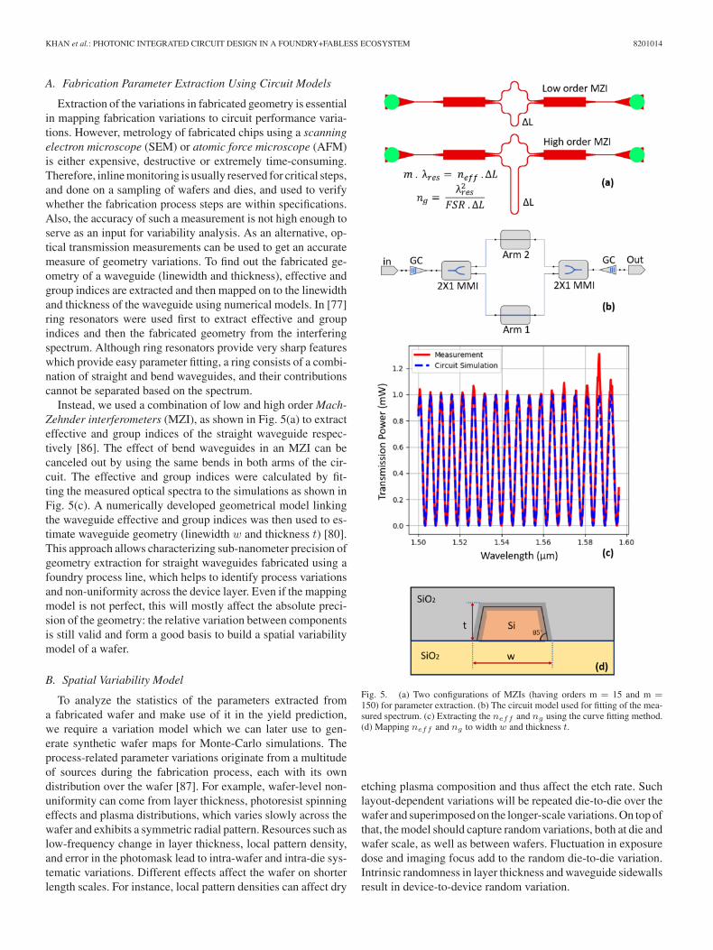
A. Fabrication Parameter Extraction Using Circuit Models
Extraction of the variations in fabricated geometry is essentialin mapping fabrication variations to circuit performance varia-tions. However, metrology of fabricated chips using a scanningelectron microscope (SEM) or atomic force microscope (AFM)is either expensive, destructive or extremely time-consuming.Therefore, inline monitoring is usually reserved for critical steps,and done on a sampling of wafers and dies, and used to verifywhether the fabrication process steps are within specifications.Also, the accuracy of such a measurement is not high enough toserve as an input for variability analysis. As an alternative, op-tical transmission measurements can be used to get an accuratemeasure of geometry variations. To find out the fabricated ge-ometry of a waveguide (linewidth and thickness), effective andgroup indices are extracted and then mapped on to the linewidthand thickness of the waveguide using numerical models. In [77]ring resonators were used first to extract effective and groupindices and then the fabricated geometry from the interferingspectrum. Although ring resonators provide very sharp featureswhich provide easy parameter fitting, a ring consists of a combi-nation of straight and bend waveguides, and their contributionscannot be separated based on the spectrum.
Instead, we used a combination of low and high order Mach-Zehnder interferometers (MZI), as shown in Fig. 5(a) to extracteffective and group indices of the straight waveguide respec-tively [86]. The effect of bend waveguides in an MZI can becanceled out by using the same bends in both arms of the cir-cuit. The effective and group indices were calculated by fit-ting the measured optical spectra to the simulations as shown inFig. 5(c). A numerically developed geometrical model linkingthe waveguide effective and group indices was then used to es-timate waveguide geometry (linewidth w and thickness t) [80].This approach allows characterizing sub-nanometer precision ofgeometry extraction for straight waveguides fabricated using afoundry process line, which helps to identify process variationsand non-uniformity across the device layer. Even if the mappingmodel is not perfect, this will mostly affect the absolute preci-sion of the geometry: the relative variation between componentsis still valid and form a good basis to build a spatial variabilitymodel of a wafer.
B. Spatial Variability Model
To analyze the statistics of the parameters extracted froma fabricated wafer and make use of it in the yield prediction,we require a variation model which we can later use to gen-erate synthetic wafer maps for Monte-Carlo simulations. Theprocess-related parameter variations originate from a multitudeof sources during the fabrication process, each with its owndistribution over the wafer [87]. For example, wafer-level non-uniformity can come from layer thickness, photoresist spinningeffects and plasma distributions, which varies slowly across thewafer and exhibits a symmetric radial pattern. Resources such aslow-frequency change in layer thickness, local pattern density,and error in the photomask lead to intra-wafer and intra-die sys-tematic variations. Different effects affect the wafer on shorterlength scales. For instance, local pattern densities can affect dry
Fig. 5. (a) Two configurations of MZIs (having orders m = 15 and m =150) for parameter extraction. (b) The circuit model used for fitting of the mea-sured spectrum. (c) Extracting the neff and ng using the curve fitting method.(d) Mapping neff and ng to width w and thickness t.
etching plasma composition and thus affect the etch rate. Suchlayout-dependent variations will be repeated die-to-die over thewafer and superimposed on the longer-scale variations. On top ofthat, the model should capture random variations, both at die andwafer scale, as well as between wafers. Fluctuation in exposuredose and imaging focus add to the random die-to-die variation.Intrinsic randomness in layer thickness and waveguide sidewallsresult in device-to-device random variation.

8201014 IEEE JOURNAL OF SELECTED TOPICS IN QUANTUM ELECTRONICS, VOL. 25, NO. 5, SEPTEMBER/OCTOBER 2019
Fig. 6. (a) Illustration of spatial variability of device parameter at different levels. (b) Top wafer maps of linewidth and thickness present the systematic intra-wafervariations under the process variation. Bottom wafer maps represent the systematic intra-die variations of linewidth and thickness.
We can decompose the total spatial variation into lot-to-lot,wafer-to-wafer, die-to-die and device-to-device variations withsystematic and random components, which can be combinedinto a hierarchical model (Fig. 6). This facilitates the characteri-zation of statistical data measured on the wafer. For instance, in[87] we show an example where the waveguide thickness suf-fers significantly larger intra-wafer systematic variation (3.0 nm)than the intra-die systematic variation (0.7 nm), while linewidthhas an intra-wafer systematic variation (8.5 nm) comparablewith its intra-die systematic variation (5.0 nm). These separatevariability components can be captured in generator models thatreplicate the essential statistical properties of the original varia-tions, using deterministic functions of stochastic noise functionswith a given correlation length. These map generators can thenbe used to perform location-aware variability analysis and yieldprediction at the circuit level. Therefore, it would present a sig-nificant added value in the future for fabs to include such mapgenerator functions into the PDK. These can be implementedas black box models, so there is no need to disclose processinformation that is considered confidential.
C. Location-Aware Yield Prediction
Waveguide-based filters are susceptible to phase variationsand coupling variations. Monte-Carlo simulations using simplerandom distributed parameters already show the sensitivity ofthe circuit, but for yield prediction, this is not realistic since thismethod does not consider location-dependency of variations. Forexample, intra-wafer thickness variations with a radial patternon the wafer affect devices in the center and near the rim dif-ferently, which is not considered by the standard Monte-Carlomethod. Also, devices located next to each other should be morecorrelated than when placed further apart.
To make realistic predictions, we incorporated informationabout the spatial variations into the Monte-Carlo method. Using
Fig. 7. (a) The generated linewidth and thickness maps used to find out theperformance of ring demultiplexers over the virtual wafer. (b) Channel spacingdistribution of the demultiplexer with rings spaced 200 µm and 30 µm apart areshown in blue and red respectively.
a virtual fabrication map (linewidth, thickness) generated bythe additive spatial variation model, the local deviations fromthe nominal values are projected onto the circuit layout and thenused to adjust the circuit model parameters of the building blocks

KHAN et al.: PHOTONIC INTEGRATED CIRCUIT DESIGN IN A FOUNDRY+FABLESS ECOSYSTEM 8201014
on the different locations. The circuit is then simulated using acircuit simulator. To analyze the variations, the circuit is thenpositioned on various wafer sites, or on different wafers [77],[78]. These simulations show that placing components closertogether in a circuit does make the circuit less sensitive to localvariations, but not to global variations. For instance, a circuitwith multiple ring filters will show a much larger spread be-tween the ring resonances when the rings are spaced further apart[77], [81].
For this technique to work, it is essential that all the infor-mation needed for this analysis is available to the circuit de-signer. This means that the foundry should be willing to providenot just compact models of the building blocks, but also wafermap generator functions of the critical fabrication parameters(or synthesized parameters that reflect the variability), as wellas the sensitivity of the component model parameters to theseparameters. Not only would this enable designers to make yieldpredictions of their circuits, but it would also allow them todesign circuits that are more tolerant of variations [85]. For in-stance, it is possible to make MZI filter circuits more robustby combining multiple waveguide geometries within the samecircuit, using the difference in sensitivity as a degree of free-dom to compensate against long-range variations in linewidthor thickness [88].
VI. MODELS FOR TIME-DOMAIN CIRCUIT SIMULATION
While passive photonic circuits are often modeled in thefrequency domain, integration in a larger circuit or systemrequires that these same circuits are then evaluated in thetime domain. However, frequency domain models are notalways easily translated into time domain models, especiallywhen the component or subcircuit has very strong dispersion.Furthermore, photonic circuits which contain nonlinear orelectro-optical building blocks can only be modeled in the timedomain, where the performance can be assessed through biterror rates (BER), eye diagrams or constellation diagrams [89],especially for telecom and datacom applications.
While the nonlinear of electro-optic components usually havegood time-domain models where the behavioral equations areimplemented into code, they are usually combined with pas-sive components into the same circuit, and the accuracy of theentire circuit simulation is determined by the combination ofmodels [36]. As the passive devices are usually parametric andcombined into larger passive subcircuits, it is not trivial to trans-late the frequency domain response into a suitable time domainmodel that can be efficiently evaluated by the circuit simulator.A suitable circuit model should meet three basic requirements:1) the models should be accurate enough with regard to the be-haviors of the actual devices, and eventually generate valuableinformation to guide circuit designs; 2) the models must be rep-resented in the time domain; 3) the models must be “compact”to make sure that the circuit simulation is efficient. How thesecriteria are met depends on the model generation strategies andthe circuit simulation approach.
Since photonic circuits and electronic circuits closely work to-gether and are integrated, the simulation should be conducted in
both domains. There are several simulation approaches to com-bine these domains discussed and implemented in both academiaand industry [36]: simulate photonic circuits and electronic cir-cuits in 1) photonic simulators; 2) electronic simulators; 3) sepa-rate electronic and photonic simulators with unidirectional dataexchange; 4) separate electronic and photonic simulators withbidirectional data exchange (Co-simulation) [90]. Therefore, be-fore building the model, we should also be aware of where themodels will be evaluated: in a photonic simulator or an electronicsimulator? This is important because the signals propagatingthrough the photonic and electronic circuits in simulations arequite different, as are the underlying equations. The photoniccircuits use bidirectional optical waves as port signals whileelectronic circuits use voltage and current at each connectionnode.
Among the four simulation approaches, the second option(adopting electronic simulators for both electronic and photoniccircuits) has shown a lot of promise [91], [92]. It is importantto note that optoelectronic devices such as detectors, amplifiers,lasers, and modulators can have both electrical and optical be-haviors, and therefore must be simulated in both domains, es-pecially if they have electrical control loops [36], [90]–[92],which indicates that it is better to simulate electrical and opticalbehaviors at the same time.
Bidirectional co-simulation is not trivial to implement and re-quires two simulators to operate in lockstep [90]. While suchtechniques are also used in analog-digital mixed-signal (AMS)design, it can raise questions about stability and conservation ofenergy when exchanging information between the two domain[89]. While it requires that electro-optical components have rep-resentation in both simulation engines, the use of co-simulationmakes it possible to use an optimized simulator for all parts ofthe circuit.
The first option (simulating everything in the optical simu-lator) can work if the optical simulator has some support forelectronic components. However, it would require designers toabandon the trusted and mature electronic simulators and mod-els, and rebuild models for electronic devices suitable for pho-tonic simulators. It would also be difficult for a new simulator tomatch the established and standardized models for a large vari-ety of electronic devices, which are natively supported by mostelectronic circuit simulators.
The opposite case, namely simulating the photonic part ofthe circuit in an electronic simulator, has more merits. A lot ofeffort has been invested in SPICE and/or Verilog-A compatiblemodels for non-linear photonic devices, such as for lasers [93]–[95], modulators [96]–[98], photodiodes [99]–[102]. The linearphotonic devices, such as waveguides, couplers, and wavelengthfilters, are normally characterized in the frequency domain andrepresented by transfer matrix (without reflection) and scatteringmatrix (with reflection). To build time-domain models for thesedevices which take into account higher-order dispersion, wave-length dependent loss, and imperfections in general, requiresthe fitting of a black-box behavioral model to the frequency re-sponse. Possible techniques include FIR based modeling method[64], or state-space model generation based on Vector Fitting[62]. Both techniques are based on scattering parameters and

8201014 IEEE JOURNAL OF SELECTED TOPICS IN QUANTUM ELECTRONICS, VOL. 25, NO. 5, SEPTEMBER/OCTOBER 2019
are widely applicable to linear passive devices. Furthermore,the models built via both techniques have the potentials to beconverted to SPICE and/or Verilog-A compatible circuit mod-els, but can also be adapted to most photonic circuit simulators[63].
The main challenge to adopting the electronic simulators forphotonic circuits is that they use inherently different signal mod-els. In electronics, signals are represented by voltages and cur-rents on nets, while in photonics they are forward and backwardoptical waves in optical waveguide modes, which are essentiallytransmission lines operating at very high (optical) frequencies.Therefore, the optical waves are often represented by their com-plex amplitude envelope which is a time-dependent complexnumber, modulated onto a high-frequency carrier wavelength.It is not straightforward to describe the complex-valued waveswith voltages and current in electronic simulators. A simplesolution is to mathematically interpret the magnitude/phase orreal/imaginary parts of the complex envelope to voltage (poten-tial) and current (flow) which is physically not sound but worksas a purely mathematically construct [91], [103]. Another pos-sible solution is to semi-physically interpret the optical waves tovoltages and current, which essentially map onto the electric andmagnetic field components of the guided optical mode(s) in thewaveguide. Like for microwave systems, the non-conservativeelectromagnetic waves can be converted to voltages and currentsthrough characteristic impedance [104], which in the optical do-main is related to the effective index.
One of the obstacles for generalizing this approach for pho-tonics is that this only simulates a fairly narrow frequency bandaround an optical carrier wave. This approximation only holds ifthere is only one coherent carrier wave. When multiple carriersare used, such as in wavelength division multiplexing (WDM)systems, each carrier should get its own signal line, and thisonly works well if the modulation bands of the carriers do notoverlap at all. When this happens, or when broadband light isused instead of monochromatic carriers, it is no longer possibleto represent the optical signal as a simple set of transmissionlines.
VII. SUMMARY AND CONCLUSION
To summarize, the design process currently used by the pho-tonic designers is still removed from the perfect process to trans-late a functional idea to the physical layout, and especially in afoundry/fabless setting where the circuit designer is decoupledfrom the fab. While the technology for the different PIC plat-forms is currently very capable of fabricating complex circuits,this scaling in complexity is currently limited on the design side.Photonic designers do not yet enjoy the comfort of a workflow,the software tools and design kits that guarantee them a first-time-right design, which is the expectation today in the elec-tronics design community. It is not surprising that we are seeingtoday a closer integration between photonic circuit design toolsand established EDA software packages.
So, following the footsteps of analog electronics, where de-signers can focus on circuits by trusting the provided standard-ized compact models, the introduction of a schematic driven
design flow for photonics is a first step in improving this pic-ture. But the success of this design flow depends very much onthe availability of circuit models. The current lack of standard-ization in model building (and their interoperability betweencircuit simulators) slows down the investments of the foundriesin sophisticated compact models. Also, the integration betweenphotonic and electronic design tools raises the question of thebest co-simulation strategies for electronics and photonics.
Depending on the PIC technologies, it is also essential thatthese models capture the effects of variability. Especially withhigh-contrast waveguide systems such as silicon, variabilityanalysis, and yield prediction techniques are desperately neededto enable scaling in complexity.
REFERENCES
[1] X. Chen et al., “The emergence of silicon photonics as a flexible tech-nology platform,” in Proc. IEEE, vol. 106, no. 12, pp. 2101–2116,Dec. 2018.
[2] R. Soref, “The past, present, and future of silicon photonics,” IEEE J.Sel. Topics Quantum Electron., vol. 12, no. 6, pp. 1678–1687, Nov./Dec.2006.
[3] T. L. Koch and U. Koren, “Semiconductor photonic integrated circuits,”IEEE J. Quantum Electron., vol. 27, no. 3, pp. 641–653, Mar. 1991.
[4] X. Duan, Y. Huang, Y. Cui, J. Wang, and C. M. Lieber, “Indium phosphidenanowires as building blocks for nanoscale electronic and optoelectronicdevices,” Nature, vol. 409, no. 6816, pp. 66–69, 2001.
[5] A. Himeno, K. Kato, and T. Miya, “Silica-based planar lightwave cir-cuits,” IEEE J. Sel. Topics Quantum Electron., vol. 4, no. 6, pp. 913–924,Nov./Dec. 1998.
[6] K. Wörhoff, R. G. Heideman, A. Leinse, and M. Hoekman, “Triplex: Aversatile dielectric photonic platform,” Adv. Opt. Technol., vol. 4, no. 2,pp. 189–207, 2015.
[7] M. U. Khan et al., “Multi-level single mode 2D polymer waveguideoptical interconnects using nano-imprint lithography,” Opt. Express,vol. 23, no. 11, pp. 14 630–14 639, 2015.
[8] D. Liang and J. E. Bowers, “Recent progress in lasers on silicon,” NaturePhoton., vol. 4, no. 8, pp. 511–517, 2010.
[9] A. E.-J. Lim et al., “Path to silicon photonics commercialization: Thefoundry model discussion,” in Silicon Photonics III. Berlin, Heidelberg,Germany: Springer, 2016, pp. 191–215.
[10] A. Rahim, T. Spuesens, R. Baets, and W. Bogaerts, “Open-accesssilicon photonics: Current status and emerging initiatives,” in Proc.IEEE, vol. 106, no. 12, pp. 2313–2330, Dec. 2018. [Online]. Available:https://ieeexplore.ieee.org/document/8540508/
[11] ASP, Australian Silicon Photonics. [Online]. Available: https://sites.google.com/view/siliconphotonics/
[12] ANT, Advanced Nano Tools. [Online]. Available: https://www.appliednt.com/nanosoi/
[13] Cornerstone, Cornerstone. [Online]. Available: https://www.cornerstone.sotonfab.co.uk/
[14] AMO GmbH, AMO GmbH. [Online]. Available: https://www.amo.de/products-services/services/
[15] AIM Photonics, AIM Photonics (SUNY). [Online]. Available: http://www.aimphotonics.com/pdk
[16] Europractice, CEA LETI. [Online]. Available: http://www.europractice-ic.com/
[17] IHP, IHP. [Online]. Available: https://www.ihp-ffo.de/en/services/overview.html
[18] Europractice, IMEC. [Online]. Available: http://www.europractice-ic.com/
[19] Silicon Photonics Platform, IMECAS. [Online]. Available:http://siplatform.cn/index.php/soi/
[20] INPHOTEC, Fondazione Inphotec. [Online]. Available: https://www.inphotec.it/
[21] Sandia National Laboratory, Sandia National Laboratory. [Online]. Avail-able: https://www.sandia.gov/mesa/nspc/index.html
[22] VTT, VTT. [Online]. Available: https://www.vtt.fi/sites/siliconphotonics/mpw-runs
[23] AMF, Advanced Micro Foundry. [Online]. Available: http://www.advmf.com/services/

KHAN et al.: PHOTONIC INTEGRATED CIRCUIT DESIGN IN A FOUNDRY+FABLESS ECOSYSTEM 8201014
[24] CompoundTek, CompoundTek. [Online]. Available: https://compoundtek.com/our-story/?noredirect=true
[25] GF, Global Foundries. [Online]. Available: https://www.globalfoundries.com/technology-solutions/silicon-photonics
[26] SMIC, Semiconductor Manufacturing International Corporation. [On-line]. Available: https://www.smics.com/en/site/multi_project
[27] TowerJazz, TowerJazz. [Online]. Available: https://towerjazz.com/manufacturing/mpw-shuttle-program/
[28] P. Muñoz et al., “Silicon nitride photonic integration platforms forvisible, near-infrared and mid-infrared applications,” Sensors, vol. 17,no. 9, 2017, Art. no. 105370B.
[29] A. Z. Subramanian et al., “Silicon and silicon nitride photonic cir-cuits for spectroscopic sensing on-a-chip,” Photon. Res., vol. 3, no. 5,pp. B47–B59, 2015.
[30] A. Rahim et al., “Expanding the silicon photonics portfolio with siliconnitride photonic integrated circuits,” J. Lightw. Technol., vol. 35, no. 4,pp. 639–649, Feb. 2017.
[31] P. Muoz et al., “Foundry developments toward silicon nitride photonicsfrom visible to the mid-infrared,” IEEE J. Sel. Topics Quantum Electron.,vol. 25, no. 5, pp. 1–13, Sep. 2019.
[32] J. Poon, “Multilayer silicon integrated photonic platforms for 3d photonicdevices and circuits,” in Proc. Integr. Photon. Res., Silicon Nanophoton-ics. 2017, pp. 1–2 .
[33] CNM CSIC, Institute of Microelectronics of Barcelona IMB CNM. [On-line]. Available: http://www.imb-cnm.csic.es/index.php/en/clean-room/
[34] LIGENTEC, LIGENTEC. [Online]. Available: https://www.ligentec.com/
[35] PIX4life, ‘BIOPIX IMEC. [Online]. Available: https://pix4life.eu/index.php/access/services
[36] W. Bogaerts and L. Chrostowski, “Silicon photonics circuit design: Meth-ods, tools and challenges,” Laser Photon. Rev., vol. 1700237, pp. 1–29,2018.
[37] K. S. Kunz and R. J. Luebbers, The Finite Difference Time Do-main Method for Electromagnetics. New York, NY, USA: CRC Press,1993.
[38] D. F. Gallagher, “Modelling photonic integrated circuits using tdtw,”in Proc. Asia Opt. Fiber Commun. Optoelectronic Expo. Conf., 2008,pp. 1–3.
[39] J.-M. Jin, The Finite Element Method in Electromagnetics. Hoboken, NJ,USA: Wiley, 2015.
[40] W. Huang, C. Xu, S.-T. Chu, and S. K. Chaudhuri, “The finite-differencevector beam propagation method: Analysis and assessment,” J. Lightw.Technol., vol. 10, no. 3, pp. 295–305, Mar. 1992.
[41] Y. Xing, U. Khan, A. R. A. Júnior, and W. Bogaerts, “Behavior model fordirectional coupler,” in Proc. Symp. IEEE Photon. Soc. Benelux, 2017,pp. 128–131.
[42] J. D. Joannopoulos, P. R. Villeneuve, and S. Fan, “Photonic crystals:Putting a new twist on light,” Nature, vol. 386, no. 6621, pp. 143–149,1997.
[43] C. M. Lalau-Keraly, S. Bhargava, O. D. Miller, and E. Yablonovitch,“Adjoint shape optimization applied to electromagnetic design,” Opt.Express, vol. 21, no. 18, pp. 21 693–21 701, 2013.
[44] A. C. Niederberger, D. A. Fattal, N. R. Gauger, S. Fan, and R. G. Beau-soleil, “Sensitivity analysis and optimization of sub-wavelength opticalgratings using adjoints,” Opt. Express, vol. 22, no. 11, pp. 12 971–12 981,2014.
[45] J. S. Jensen and O. Sigmund, “Topology optimization for nano-photonics,” Laser Photon. Rev., vol. 5, no. 2, pp. 308–321, 2011.
[46] P. I. Borel et al., “Topology optimization and fabrication of pho-tonic crystal structures,” Opt. Express, vol. 12, no. 9, pp. 1996–2001,2004.
[47] S. Molesky et al., “Inverse design in nanophotonics,” Nature Photon.,vol. 12, no. 11, pp. 659–670, 2018.
[48] M. Rakowski et al., “A 420 Gb/s WDM ring-based hybrid CMOS siliconphotonics transceiver,” in Proc. Dig. Tech. Papers—IEEE Int. Solid-StateCircuits Conf., vol. 58, pp. 408–409, 2015.
[49] J. Sun, E. Timurdogan, A. Yaacobi, E. S. Hosseini, and M. R.Watts, “Large-scale nanophotonic phased array,” Nature, vol. 493,no. 7431, pp. 195–199, 2013. [Online]. Available: http://www.nature.com/doifinder/10.1038/nature11727
[50] SMART Photonics. [Online]. Available: https://smartphotonics.nl/[51] D. F. Welch et al.,“Large-scale inp photonic integrated circuits: Enabling
efficient scaling of optical transport networks,” IEEE J. Sel. Topics Quan-tum Electron., vol. 13, no. 1, pp. 22–31, Jan./Feb. 2007.
[52] X. Leijtens, “Jeppix: The platform for indium phosphide-based photon-ics,” IET Optoelectronics, vol. 5, no. 5, pp. 202–206, 2011.
[53] P. P. Absil et al., “Silicon photonics integrated circuits: A manu-facturing platform for high density, low power optical I/O’s,” Opt.Express, vol. 23, no. 7, pp. 9369–9378, 2015. [Online]. Available:http://www.opticsexpress.org/abstract.cfm?URI=oe-23-7-9369
[54] X. Wang et al., “Large-scale silicon photonics circuit design,”in Proc. SPIE, vol. 9277, 2014, pp. 1–10. [Online]. Available:http://dx.doi.org/10.1117/12.2071958
[55] M. Streshinsky et al., “The road to affordable, large-scale silicon pho-tonics,” Opt. Photon. News, vol. 24, no. 9, pp. 32–39, 2013. [Online].Available: https://www.osapublishing.org/abstract.cfm?URI=opn-24-9-32
[56] Lumerical Solutions, Inc., InterConnect. [Online]. Available: http://www.lumerical.com/tcad-products/interconnect/
[57] VPIPhotonics, VPIcomponentmaker Photonic Circuits. [Online]. Avail-able: http://www.vpiphotonics.com/CMPhotonicCircuits.php
[58] Filarete, ASPIC photonic circuit simulator. [Online]. Available:http://www.aspicdesign.com/
[59] Photon Design, PICWave, a photonic integrated circuit (PIC) de-sign and simulation tool. [Online]. Available: http://www.photond.com/products/picwave.htm
[60] Optiwave, Design software for photonics. [Online]. Available:http://www.optiwave.com
[61] Touchstone File format Specification. [Online]. Available:https://ibis.org/connector/touchstone_spec11.pdf
[62] Y. Ye, D. Spina, Y. Xing, W. Bogaerts, and T. Dhaene, “Numer-ical modeling of linear photonic system for accurate and efficienttime-domain simulations,” Photon. Res., vol. 6, no. 6, pp. 560–573,Jun. 2018.
[63] Y. Ye, D. Spina, W. Bogaerts, and T. Dhaene, “Baseband macromodel-ing of linear photonic circuits for time-domain simulations,” J. Lightw.Technol., vol. 37, no. 4, pp. 1364–1373, Feb. 2019.
[64] S. Mingaleev, A. Richter, E. Sokolov, C. Arellano, and I. Koltchanov,“Towards an automated design framework for large-scale photonic in-tegrated circuits,” Proc. SPIE, vol. 9516, pp. 951602–951602-15, 2015.[Online]. Available: http://dx.doi.org/10.1117/12.2182230
[65] J. Pond et al., “A complete design flow for silicon photonics,” Proc. SPIE,vol. 913310, pp. 913310–913310-17, 2014.
[66] W. Bogaerts, M. Fiers, M. Sivilotti, and P. Dumon, “The IP-KISS photonic design framework,” in Proc. Opt. Fiber Commun.Conf., 2016, pp. 2–4. [Online]. Available: http://www.osapublishing.org/abstract.cfm?URI=OFC-2016-W1E.1
[67] E. Ghillino et al.,“The synopsys software environment to designand simulate photonic integrated circuits: A case study for 400 gtransmission,” in Proc. 20th Int. Conf. Transparent Opt. Netw., 2018,pp. 1–4.
[68] P. Dumais, D. J. Goodwill, D. Celo, J. Jiang, and E. Bernier, “Three-modesynthesis of slab Gaussian beam in ultra-low-loss in-plane nanophotonicsilicon waveguide crossing,” in Proc. 14th Conf. Group IV Photon., 2017,pp. 97–98.
[69] W. Bogaerts, P. Dumon, D. Van Thourhout, and R. Baets, “Low-loss,low-crosstalk crossings for SOI nanophotonic waveguides,” Opt. Lett.,vol. 32, no. 19, pp. 2801–2803, 2007.
[70] Mentor Graphics, Calibre - IC verification. [Online]. Available:http://www.mentor.com
[71] Cadence inc.s, Physical verification system. [Online]. Available:https://www.cadence.com
[72] Synopsys inc., IC validator. [Onlinbe]. Available: https://www.synopsys.com/implementation-and-signoff/physical-verification/ic-validator.html
[73] R. Cao et al., “Silicon photonics design rule checking: Application ofa programmable modeling engine for non-manhattan geometry verifi-cation,” in Proc. 22nd Int. Conf. Very Large Scale Integration, 2014,pp. 1–6.
[74] G. P. Agrawal, Fiber-Optic Communication Systems, vol. 222. Hobo-ken, NJ, USA: Wiley, 2012. [Online]. Available: https://books.google.com.br/books?id=yGQ4n1-r2eQC
[75] S. Mingaleev, S. G. Savitski, E. S. Sokolov, I. G. Koltchanov, andA. Richter, “Layout-aware schematic-driven design methodology forphotonic integrated circuits,” in Proc. Eur. Conf. Integr. Opt., 2016,pp. 17:45–19:15.
[76] L. Chrostowski et al., “Design and simulation of silicon photonicschematics and layouts,” Proc. SPIE, vol. 9891, 2016, Art. no. 98911411.
[77] Z. Lu et al., “Performance prediction for silicon photonics integratedcircuits with layout-dependent correlated manufacturing variability,”Opt. Express, vol. 25, no. 9, pp. 9712–9733, 2017. [Online]. Available:https://www.osapublishing.org/abstract.cfm?URI=oe-25-9-9712

8201014 IEEE JOURNAL OF SELECTED TOPICS IN QUANTUM ELECTRONICS, VOL. 25, NO. 5, SEPTEMBER/OCTOBER 2019
[78] W. Bogaerts, U. Khan, and Y. Xing, “Layout-aware yield prediction ofphotonic circuits,” in Proc. IEEE Int. Conf. Group IV Photon., Cancun,Mexico, 2018, pp. 93–94.
[79] L. Chrostowski et al., “Schematic driven silicon photonics design,” inProc. SPIE OPTO, vol. 9751, 2016, pp. 1–14.
[80] Y. Xing, J. Dong, S. Dwivedi, U. Khan, and W. Bogaerts, “Accurateextraction of fabricated geometry using optical measurement,” Photon.Res., vol. 6, no. 11, pp. 1008–1020, 2018.
[81] Y. Xing et al., “From parameter extraction , variability models to yieldprediction,” in Proc. Latin Amer. Opt. Photon. Conf., 2018, p. W3E.1.
[82] A. Waqas, S. Member, D. Melati, and A. Melloni, “Sensitivity analysisand uncertainty mitigation of photonic integrated circuits,” J. Lightw.Technol., vol. 35, no. 17, pp. 3720–3728, Sep. 2017.
[83] D. Melati, A. Waqas, D.-x. Xu, and A. Melloni, “Genetic algorithm andpolynomial chaos modelling for performance optimization of photoniccircuits under manufacturing variability,” in Proc. Opt. Fiber Comm.Conf. Expo., vol. 1, 2018, pp. 23–25.
[84] D. Cassano, F. Morichetti, and A. Melloni, “Statistical analysisof photonic integrated circuits via polynomial-chaos expansion,” inProc. Adv. Photon., 2013, p. JT3A.8. [Online]. Available: http://www.opticsinfobase.org/abstract.cfm?URI=IPRSN-2013-JT3A.8
[85] W. Bogaerts, Y. Xing, and U. Khan, “Layout-aware variability analysis,yield prediction, and optimization in photonic integrated circuits,” IEEEJ. Sel. Topics Quantum Electron., vol. 25, no. 5, pp. 1–13, Sep. 2019.
[86] S. Dwivedi et al., “Experimental extraction of effective refractive indexand thermo-optic coefficients of silicon-on-insulator waveguides usinginterferometers,” J. Lightw. Technol., vol. 33, no. 21, pp. 4471–4477,Nov. 2015.
[87] Y. Xing, J. Dong, U. Khan, and W. Bogaerts, “Hierarchical model forspatial variations of integrated photonics,” in Proc. IEEE Int. Conf. GroupIV Photon. Cancun, Mexico, 2018, pp. 1–2.
[88] S. Dwivedi, H. D’heer, and W. Bogaerts, “Maximizing fabrication andthermal tolerances of all-silicon FIR wavelength filters,” IEEE Photon.Technol. Lett., vol. 27, no. 8, pp. 871–874, Apr. 2015.
[89] M. Heins et al., Design Flow Automation for Silicon Photonics: Chal-lenges, Collaboration, and Standardization. Berlin, Heidelberg, Ger-many: Springer, 2016, pp. 99–156.
[90] A. Farsaei et al., “A novel and scalable design methodology for the sim-ulation of photonic integrated circuits,” in Proc. Adv. Photon., 2016,p. JTu4A.2.
[91] C. Sorace-Agaskar, J. Leu, M. R. Watts, and V. Stojanovic, “Electro-optical co-simulation for integrated CMOS photonic circuits withVerilogA,” Opt. Express, vol. 23, no. 21, pp. 27 180–27 203, Oct.2015. [Online]. Available: http://www.opticsexpress.org/abstract.cfm?URI=oe-23-21-27180
[92] J. C. Leu, “Integrated silicon photonic circuit simulation,” Ph.D. dis-sertation, Dept. Elect. Eng. Comput. Sci., MIT, Cambridge, MA, USA,2018.
[93] P. V. Mena, J. J. Morikuni, S. Kang, A. V. Harton, and K. W. Wyatt,“A comprehensive circuit-level model of vertical-cavity surface-emittinglasers,” J. Lightw. Technol., vol. 17, no. 12, pp. 2612–2632, Dec. 1999.
[94] M. Belkin and V. Iakovlev, “Microwave-band circuit-level semiconduc-tor laser modeling,” in Proc. IEEE Eur. Modelling Symp., Oct. 2015,pp. 443–445.
[95] H. R. Yousefvand, “A versatile physics-based circuit model for mid-infrared quantum cascade lasers,” J. Lightw. Technol., vol. 34, no. 3,pp. 1031–1037, Feb. 2016.
[96] H. Bahrami, H. Sepehrian, C. S. Park, L. A. Rusch, and W. Shi, “Time-domain large-signal modeling of traveling-wave modulators on SOI,” J.Lightw. Technol., vol. 34, no. 11, pp. 2812–2823, Jun. 2016.
[97] S. Tanaka, T. Usuki, and Y. Tanaka, “Accurate SPICE model of forward-biased silicon PIN machzehnder modulator for an energy-efficient mul-tilevel transmitter,” J. Lightw. Technol., vol. 36, no. 10, pp. 1959–1969,May 2018.
[98] B. Wang et al., “A compact Verilog—A model of silicon carrier-injectionring modulators for optical interconnect transceiver circuit design,” J.Lightw. Technol., vol. 34, no. 12, pp. 2996–3005, Jun. 2016.
[99] Y. M. El-Batawy and M. J. Deen, “Analysis, circuit modeling, and opti-mization of mushroom waveguide photodetector (mushroom-WGPD),”J. Lightw. Technol., vol. 23, no. 1, pp. 423–431, Jan. 2005.
[100] M. Jalali, M. K. Moravvej-Farshi, S. Masudy-Panah, and A. Nabavi, “Anequivalent lumped circuit model for thin avalanche photodiodes withnonuniform electric field profile,” J. Lightw. Technol., vol. 28, no. 23,pp. 3395–3402, Dec. 2010.
[101] M. Piels, A. Ramaswamy, and J. E. Bowers, “Nonlinear modelingof waveguide photodetectors,” Opt. Express, vol. 21, no. 13, pp.15 634–15 644, Jul. 2013. [Online]. Available: http://www.opticsexpress.org/abstract.cfm?URI=oe-21-13-15634
[102] D. Dai, M. Piels, and J. E. Bowers, “Monolithic germanium/silicon pho-todetectors with decoupled structures: Resonant APDs and UTC photo-diodes,” IEEE J. Sel. Topics Quantum Electron, vol. 20, no. 6, pp. 43–56,Nov. 2014.
[103] P. Gunupudi, T. Smy, J. Klein, and Z. J. Jakubczyk, “Self-consistentsimulation of opto-electronic circuits using a modified nodal analysisformulation,” IEEE Trans. Adv. Packag., vol. 33, no. 4, pp. 979–993,Nov. 2010.
[104] R. B. Marks and D. F. Williams, “A general waveguide circuit theory,”J. Res. Nat. Inst. Standards Technol., vol. 97, no. 5, p. 533, 1992.
Muhammad Umar Khan received the Ph.D. degreefrom Tyndall National Institute, University CollegeCork, Cork, Ireland, for his work on “Design and im-plementation of microstructures with refractive indexcontrast for optical interconnects and sensing appli-cations.” After completing his Ph.D., he joined Pho-tonics Research Group at Ghent University—IMEC,Belgium, as a Postdoctoral Researcher. His currentresearch interests include compact models, variabil-ity aware design, parameters extraction, and pro-grammable circuits.
Yufei Xing received the bachelor’s degree in opti-cal engineering from Zhejiang University, China, in2011. He received the master’s degree from EuropeanMaster of Science in Photonics from Ghent Univer-sity, Belgium, in 2013. He is currently working towardthe Ph.D. degree with the Photonics Research Groupat Ghent University—IMEC. His current research in-terests include variability aware design, compact cir-cuit models, and parameter extraction.
Yinghao Ye received the bachelor’s and the master’sdegree in electronic engineering from the Xidian Uni-versity, Xi’an, China, in 2011 and 2014, respectively.He is currently working toward the Ph.D. degree withthe Department of Information Technology at GhentUniversity, Ghent, Belgium. His current research in-terests include modeling of photonic and electroniccircuits for time-domain simulations and variabilityanalysis.
Wim Bogaerts received the Ph.D. degree in the mod-eling, design, and fabrication of silicon nanophotoniccomponents at Ghent University, Ghent, Belgium, in2004. During this work, he started the first silicon pho-tonics process on IMEC’s 200mm pilot line, whichformed the basis of the multiproject-wafer serviceePIXfab.
In 2014, he co-founded Luceda Photonics, a spin-off company of Ghent University, IMEC, and theUniversity of Brussels (VUB), Brussels, Belgium.Luceda Photonics develops unique software solutions
for silicon photonics design, using the IPKISS design framework.Since 2016, he has been Full-Time Professor with Ghent University, looking
into novel topologies for large-scale programmable photonic circuits, supportedby a consolidator grant of the European Research Council (ERC). He is also aProfessor with the Photonics Research Group at Ghent University–IMEC. Hehas a strong interest in telecommunications, information technology, and appliedsciences. His current research focuses on the challenges for large-scale siliconphotonics: Design methodologies and controllability of complex photonic cir-cuits. Dr. Bogaerts is a member of Optical Society of America (OSA) and SPIE.