perovskite solar cells - ohio university
TRANSCRIPT

1
Encyclopedia of Chemical Processing
Copyright © 2018 by Taylor & Francis. All rights reserved.
Perovskite Solar Cells
Juvinch R. Vicente and Jixin ChenDepartment of Chemistry and Biochemistry, Nanoscale and Quantum Phenomena Institute, Ohio University, Athens, Ohio, U.S.A.
AbstractSolar energy is projected to be one of the ultimate sustainable energy resources. Solar cells are devices that directly convert photon energy into electricity. One of the emerging techniques is per-ovskite solar cells (PSCs), which have already shown a great promise in its infancy stage. This entry discusses a brief overview of PSCs, including operation and critical material properties, the general fabrication methods employed in laboratory scale, the feasible upscaling fabrication methods currently being investigated, and finally, the existing challenges and opportunities of this technology.
KeywordsSolar energyOrganic-inorganic hybrid perovskiteThin-film photovoltaic devicesPower conversion efficiency
INTRODUCTION
Perovskite solar cells (PSCs) is considered as a promising candidate for future cost-effective photovoltaics. The key component in a PSC is a thin-layer of organic-inorganic hybrid perovskite (OHP), which has excellent properties in optical absorption and charge transport, and is compatible with low-cost solution-based processing. OHPs were ini-tially demonstrated in 2009 by Miyasaka as the sensi-tizers for a mesoporous photoelectrode in dye- sensitized solar cells (DSSCs), with a minimal power conversion efficiency (PCE) of 3.8%, and a poor stability due to the liquid-based electrolytes. In 2012, all-solid-state PSC with much improved stability and PCE was introduced by Park and Graetzel. In 2013, Snaith further demonstrated that OHPs can be operated as an efficient absorber layer in planar architectures. Since then, rapid progress has been achieved for PSCs with PCE now reaching over 22% in the middle of 2017, and more than one-year stability with over 11.2% PCE for 100 cm2 modules in the early 2017.
SOLAR CELL WORKING PRINCIPLE
Solar cells are devices that facilitate the conversion of sun-light directly into electrical energy. The main processes involved in solar cell operations generally include (with an example of PSC given in Fig. 1):[1]
1. Generation of free-charge carriers (electrons and holes) in the absorber layer after light absorption.
2. Transportation of the free-charge carriers to their respective electrodes through selective interfaces for either electrons or holes.
3. Collection of the free-charge carriers in the electrodes, which provides power to an external load.
The energy generated from solar cells are derived from the photons coming from the sun. According to the Planck-Einstein relation, the energy of a single photon is expressed as:
λ=E hc
ph
Where: h is the Planck’s constant, c is the speed of light in vacuum, λ is the wavelength of photons.
In most cases, Eph
is expressed in terms of elec-tron-volts (eV) since the values in joules are too small (1 eV = 1.602 × 10⁻¹⁹ J). The energy of the majority of photons coming from the sun ranges from 0.5 to 4 eV originated from the black-body radiation of a solar sur-face temperature of ~5800 K.[2] The actual distribution is dependent on variables such as time of the day, altitude, and atmospheric conditions due to the absorption and scat-tering of the atmosphere. In testing solar cells, AM1.5G spectrum is often used as a standard, which integrates to 1000 W/m2 of total energy flux.[3]
DOI: 10.1081/E-ECHP-140000328
CH_005-140000328.indd 1 21/08/18 8:55 PM

2 Perovskite Solar Cells
The number of free-charge carriers or photocurrent generated within the absorber layer depends mainly on its bandgap (E
g), that is the energy difference between
its ground (valence band of a semiconductor) and excited (conduction band) states. Ideally, only photons with energies equal or higher than the bandgap get absorbed (E
ph ≥ E
g) to produce free-charge carriers, while photons
with lower energies are transmitted. In principle, the lower the bandgap, the higher the photocurrent. However, band-gap also restricts the energy of each free-charge carrier or its photovoltage, and the higher the bandgap, the higher is the photovoltage.[4] The electrical energy per unit solar cell area is the product of the photocurrent and the photovolt-age, E
e = IV/area (W/m2).[2] The solar efficiency is defined
the electrical energy over the total solar energy received by the solar cell: PCE ≡ E
e/1000 for the AM1.5G spectrum.
The PCE limit of a single p-n junction under AM1.5G has been calculated to be the Shockley–Queisser limit, 33.7% with a bandgap of 1.34 eV.[2] Thus, the optimum bandgap of absorber materials used in solar cells ranges between 1 and 1.5 eV to approach the best condition of this limit. Table 1 summarizes the bandgap of photovoltaic materials including perovskites used in existing PV technologies and their reference record PCE.
To generate photocurrent, the free electrons and holes have to be transported and collected through their respec-tive electrodes, otherwise, they will eventually recombine in the absorber layer, in which case the energy they carry is lost into heat and/or emission.[10] In PSCs, charge transports are achieved by electron transport layer (ETL) and hole transport layer (HTL) (Fig. 1). ETL is made of n-type semiconductor materials that has high conductivity towards electrons, allowing electrons to flow to the cathode while effectively blocking holes. On the other side of the device, HTL is made of p-type semiconductor, allowing the holes
to flow to the anode while effectively blocking the flow of electrons, due to its high conductivity towards holes.[11]
DEVICE ARCHITECTURE
Perovskite solar cell (PSC) was initially developed based on dye-sensitized solar cell architecture; then planar thin film device architecture was later adapted. Until now, meso-scopic scaffolds and planar heterojunctions are still the two major architectures (Fig. 2). In mesoscopic architectures, the scaffold can be active in electron transport (in sensitized mesoporous structure, Fig. 2A), or completely insulating (in meso-superstructured solar cells, Fig. 2B) that are not involved in charge transport. Planar architecture can be either conventional or inverted depending on the relative positions of the component layers (Fig. 2C and D).
Sensitized Mesoporous-TiO2 Structure
OHPs were initially incorporated as a sensitizer in dye-sensitized solar cells (Fig. 2A).[12] In this architecture, nanoparticles of MAPbI
3 and MAPbBr
3 were infiltrated
into the mesoporous TiO2, with a liquid electrolyte hole
transport layer, achieving a champion PCE of 3.8% with high optical absorption.[12] One of the major drawbacks of this architecture is the associated poor stability, due to the dissolution of perovskite layer to the liquid electrolyte.[13] To address this issue, the liquid electrolyte was replaced with solid-state hole transport material, 2,2′,7,7′-tetrakis (N,N′-di-p-methoxyphenylamine)-9,9′-spirobifluorene (spiro-OMeTAD), which greatly improved the PCE to 9%, and more importantly the stability of the device.[14] To this date, this solid-state hole transport material is still exceptional in achieving high performance PSCs.
Meso-superstructured Solar Cells (MSSCs)
In 2012, Snaith et al. replaced the mesoporous TiO2 (m-TiO
2)
from DSSC with a wide bandgap and insulating mesoporous alumina (m-Al
2O
3) that is deposited onto a thin compact TiO
2
Fig. 1 Basic processes involved in the photovoltaic conversion of solar energy (hν) to electrical energy in a PSC. TCS, transpar-ent conductive substrates; ETL, electron transport layer; HTL, hole transport layer; CB, conduction band; VB, valence band.
Table 1 Photovoltaic semiconductors employed in various single-junction PV technologies with their typical bandgaps and the PCE records for a 1-cm2 cell
Material Bandgap (eV) Efficiency (%)
Silicon 1.12[5] 26.7[6]
GaAs 1.42[5] 28.8[6]
CIGS 1.0–2.4[5] 21.7[6]
CdTe 1.43[5] 21.0[6]
CZTS 1.0–1.6[5] 10.0[6]
Organic 1.0–2.1[7] 11.2[6]
DSSC 1.50–2.5 11.9[6]
Perovskite 1.25–2.23[8,9] 19.7[6]
CH_005-140000328.indd 2 21/08/18 8:55 PM

Perovskite Solar Cells 3
film on FTO substrate. This new architecture was referred to as meso-superstructured solar cells (MSSCs) (Fig. 2B). Their measurements revealed that the charge transport using m-Al
2O
3 structure was faster by a factor >101 compared to
the m-TiO2 based devices. In this report, they concluded that
the mesoporous structure does not serve a significant role for charge transport in the device. Rather, it simply acts as a scaffold in which the perovskite is structured.[15]
Planar Heterojunction
By completely removing the mesoporous scaffold, it was demonstrated that OHP can be incorporated to a much simpler planar architecture (Fig. 2C). Before optimization, this architecture initially delivered a PCE of ~5%.[16] The planar architecture was further improved by fabricating the perovskite material via vapor-deposition methods, as a means of creating uniform flat films of the mixed halide perovskite CH
3NH
3PbI
3-xCl
x.[17] By obtaining a highly uni-
form compact perovskite layer, the PCE of planar architec-ture PSCs was raised to over 15%. The planar architecture gets rid of the infiltration problems of the perovskite and
hole transport material in the mesoporous scaffold, which improves the device reproducibility.[18] Early reports in planar PSCs emphasize a uniform and compact perovskite layer for high device PCE, which triggered the development of various deposition techniques.[18,19]
MATERIALSPerovskite Absorber Layer
General structure, ABX3
Perovskite is the crystal structure name of a calcium titanium oxide mineral composed of calcium titanate (CaTiO
3).[21] This name is adapted by the solar cell com-
munity to specify a group of organic-inorganic hybrid perovskites (OHPs). They have a general formula of ABX
3 with the organic component (A = CH
3NH
3+) in the
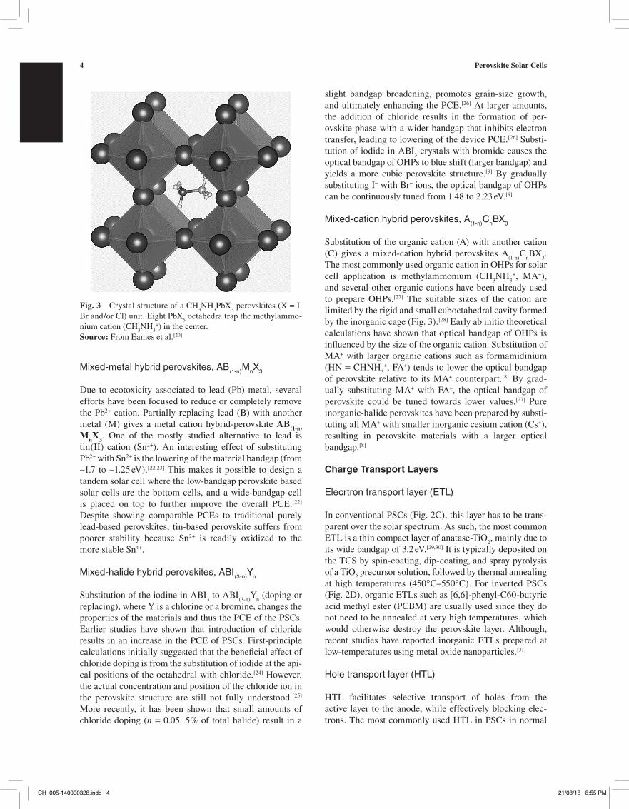
cuboctahedral site (the center of Fig. 3) and inorganic components (B = Pb2+, X = I−, Br−, Cl−) in the octahedral structure, with metal center and halide corners (Fig. 3).[20] The chemistry of the organic and inorganic components can be altered to allow tuning of its crystal, optical, and electronic properties.[9]
Fig. 2 Schematic diagrams of architectures employed in PSCs. (A) Sensitized-mesoporous scaffold, (B) meso-superstructured architecture, (C) conventional planar architecture, (D) inverted planar architecture.
CH_005-140000328.indd 3 21/08/18 8:55 PM
4 Perovskite Solar Cells
Mixed-metal hybrid perovskites, AB(1-n)MnX3
Due to ecotoxicity associated to lead (Pb) metal, several efforts have been focused to reduce or completely remove the Pb2+ cation. Partially replacing lead (B) with another metal (M) gives a metal cation hybrid-perovskite AB(1-n)
MnX3. One of the mostly studied alternative to lead is tin(II) cation (Sn2+). An interesting effect of substituting Pb2+ with Sn2+ is the lowering of the material bandgap (from ~1.7 to ~1.25 eV).[22,23] This makes it possible to design a tandem solar cell where the low-bandgap perovskite based solar cells are the bottom cells, and a wide-bandgap cell is placed on top to further improve the overall PCE.[22] Despite showing comparable PCEs to traditional purely lead-based perovskites, tin-based perovskite suffers from poorer stability because Sn2+ is readily oxidized to the more stable Sn4+.
Mixed-halide hybrid perovskites, ABI(3-n)Yn
Substitution of the iodine in ABI3 to ABI
(3-n)Y
n (doping or
replacing), where Y is a chlorine or a bromine, changes the properties of the materials and thus the PCE of the PSCs. Earlier studies have shown that introduction of chloride results in an increase in the PCE of PSCs. First-principle calculations initially suggested that the beneficial effect of chloride doping is from the substitution of iodide at the api-cal positions of the octahedral with chloride.[24] However, the actual concentration and position of the chloride ion in the perovskite structure are still not fully understood.[25] More recently, it has been shown that small amounts of chloride doping (n = 0.05, 5% of total halide) result in a
slight bandgap broadening, promotes grain-size growth, and ultimately enhancing the PCE.[26] At larger amounts, the addition of chloride results in the formation of per-ovskite phase with a wider bandgap that inhibits electron transfer, leading to lowering of the device PCE.[26] Substi-tution of iodide in ABI
3 crystals with bromide causes the
optical bandgap of OHPs to blue shift (larger bandgap) and yields a more cubic perovskite structure.[9] By gradually substituting I− with Br− ions, the optical bandgap of OHPs can be continuously tuned from 1.48 to 2.23 eV.[9]
Mixed-cation hybrid perovskites, A(1-n)CnBX3
Substitution of the organic cation (A) with another cation (C) gives a mixed-cation hybrid perovskites A
(1-n)C
nBX
3.
The most commonly used organic cation in OHPs for solar cell application is methylammonium (CH
3NH
3+, MA+),
and several other organic cations have been already used to prepare OHPs.[27] The suitable sizes of the cation are limited by the rigid and small cuboctahedral cavity formed by the inorganic cage (Fig. 3).[28] Early ab initio theoretical calculations have shown that optical bandgap of OHPs is influenced by the size of the organic cation. Substitution of MA+ with larger organic cations such as formamidinium (HN = CHNH
3+, FA+) tends to lower the optical bandgap
of perovskite relative to its MA+ counterpart.[8] By grad-ually substituting MA+ with FA+, the optical bandgap of perovskite could be tuned towards lower values.[27] Pure inorganic-halide perovskites have been prepared by substi-tuting all MA+ with smaller inorganic cesium cation (Cs+), resulting in perovskite materials with a larger optical bandgap.[8]
Charge Transport Layers
Elecrtron transport layer (ETL)
In conventional PSCs (Fig. 2C), this layer has to be trans-parent over the solar spectrum. As such, the most common ETL is a thin compact layer of anatase-TiO
2, mainly due to
its wide bandgap of 3.2 eV.[29,30] It is typically deposited on the TCS by spin-coating, dip-coating, and spray pyrolysis of a TiO
2 precursor solution, followed by thermal annealing
at high temperatures (450°C–550°C). For inverted PSCs (Fig. 2D), organic ETLs such as [6,6]-phenyl-C60-butyric acid methyl ester (PCBM) are usually used since they do not need to be annealed at very high temperatures, which would otherwise destroy the perovskite layer. Although, recent studies have reported inorganic ETLs prepared at low-temperatures using metal oxide nanoparticles.[31]
Hole transport layer (HTL)
HTL facilitates selective transport of holes from the active layer to the anode, while effectively blocking elec-trons. The most commonly used HTL in PSCs in normal
Fig. 3 Crystal structure of a CH3NH
3PbX
3 perovskites (X = I,
Br and/or Cl) unit. Eight PbX6 octahedra trap the methylammo-
nium cation (CH3NH
3+) in the center.
Source: From Eames et al.[20]
CH_005-140000328.indd 4 21/08/18 8:55 PM

Perovskite Solar Cells 5
architecture (Fig. 2A–C) is a p-type organic molecule, 2,2ʹ,7,7ʹ-Tetrakis-(N,N-di-4-methoxyphenylamino)- 9,9ʹ-spirobifluorene (spiro-MeOTAD).[32] Spiro-MeOTAD is doped with lithium bis(trifluoromethylsulphonyl)imide (Li-TFSI) to enhance hole mobility and conductivity. It is normally coated onto the active layer by spin-coating its solution (using chlorobenzene as solvent) and allowed to oxidize in dry air or oxygen. In inverted architecture (Fig. 2D), PEDOT:PSS is often used, as well as thin films of amorphous nickel oxide (NiO
x).
Electrodes
Transparent conductive substrates (TCS)
The main purpose of transparent conductive substrates (TCS) is to serve as one of the electrode contacts of the device. In most cases, light enters the solar cell through the supporting substrate. For this reason, the substrate must be transparent over the solar spectrum to minimize the loss of photons before reaching the absorber layer. Typical examples used in PSCs are fluorine-doped tin(II) oxide (FTO) and indium-doped tin(II) oxide (ITO) coated substrates. The substrates could be made of rigid material like glass or flexible like polymer-based materials.[33–35]
Counter electrode
Most commonly used counter metal electrode in PSCs are gold (Au), silver (Ag), aluminum (Al), and platinum (Pt), because of their excellent electrical conductivity. The choice for appropriate counter electrodes is usually based on the alignment of its work function with the valence band of the HTL (or conduction band of ETL for inverted PSCs). With this consideration, Au is usually used for normal PSCs with spiro-MeOTAD as HTL. Recently, more cost- effective alternative counter electrodes based on non-precious metals and carbon materials have also been explored.[36,37]
FABRICATION METHODS
To this date, fabrication of PSCs is still mainly done in the laboratory scale using solution-based processes and vapor-deposition techniques.[17,38–40] The goal mainly is to obtain homogeneous and dense layers of perovskite films that cover the substrate completely. Although not all laboratory scale processes can be translated directly to commercially viable methods, they paved the way to the understanding of the perovskite formation and the mate-rials’ critical properties.[41] This served as the basis for the development of feasible upscaling techniques, which are discussed later in this section. In this section, the most commonly used perovskite material, CH
3NH
3PbI
3, will be
used as an example to describe the techniques. However, the techniques described could be optimized to facilitate
fabrication of perovskites with varying compositions as described in earlier sections.
Solution-Based Processes
One of the main advantages of PSCs is their compatibility to solution-based fabrication, which generally translates to cost-effective upscaling methods. Solution-based fabrication of hybrid perovskite can be done by single step deposition or sequential coating of the precursor materials (Fig. 4).[42]
In a single deposition method, equivalent amounts of both precursors (i.e., CH
3NH
3I and PbI
2) are dissolved in
a suitable organic solvent, like N,N-dimethylformamide (DMF), dimethyl sulfoxide (DMSO), or γ-butyrolactone. This precursor solution is then spin-coated onto an elec-trode followed by thermal annealing at about 100°C to evaporate excess solvent and by-products. By convective self-assembly, a dense layer of well-crystallized perovskite material is formed on the substrate.[43] The composition of the precursor solution, the solvent used, the spin-coating parameters, and the thermal annealing conditions are var-ied to optimize the film properties.[44–46] In two-step solu-tion process, a hot solution of PbI
2 in an organic solvent
is spin-coated on the substrate first, followed by thermal annealing to form a uniform PbI
2 thin film layer. Subse-
quently, the resulting PbI2 film is exposed to the CH
3NH
3I
solution, by dipping or by spin-coating, which leads to the rapid formation of the perovskite film.[38–40]
Vapor-Based Processes
In the earlier stages of solution-based processes, partic-ularly one-step coating methods, perovskite materials
Fig. 4 One-step (A) and two-step (B) sequential deposition of CH
3NH
3PbI
3 perovskite. In single step coating, CH
3NH
3I and
PbI2 were mixed in N,N-dimethylacetamide (DMA) and spin-
coated on FTO/TiO2 substrate followed by thermal annealing.
In sequential method, a solution of PbI2 was first coated on the
substrate followed by spin-coating of the CH3NH
3I solution and
final annealing treatment.Source: From Im et al.[38]
CH_005-140000328.indd 5 21/08/18 8:55 PM

6 Perovskite Solar Cells
deposited on substrates suffered from uncontrolled per-ovskite formation and large morphological variations between devices.[47] Vapor deposition techniques were later introduced to address this problem.[17] The most commonly used vapor-deposition technique is by co-evaporation. In this method, a clean electrode substrate is placed inside a vacuum chamber at a fixed distance above both precursors (PbI
2 and CH
3NH
3I) that are contained in separate cruci-
bles (Fig. 5).[17] The typical pressure during deposition is about 10−5 to 10−6 Torr.[48] The precursors are then heated until they evaporate or sublimate. The vapors from both precursors condense on the substrate forming smooth and compact CH
3NH
3PbI
3 perovskite layers. The thickness
of the forming perovskite film is monitored typically by a quartz crystal microbalance (QCM) mounted inside the vacuum chamber close to the substrate.[48]
UPSCALING METHODS
Feasible upscaling methods for PSCs fabrication are mainly based on solution processes described in the pre-vious section, mainly due to its superior practicability and simplicity over vapor-deposition based processes. Exam-ples of these solution-compatible methods include electro-deposition, spray-coating, inkjet printing, screen printing, and blade coating. Spin-coating, the most commonly used technique at laboratory scale, can be hardly translated to large-scale fabrication because extreme motion is difficult to control and a large amount of material is wasted.[41]
Blade coating
Blade coating refers to a family of coating processes where a liquid layer comes from the shallow channel formed between a stationary blade and moving substrate, or a moving blade and stationary substrate. The well- defined thickness of the resulting film is mainly controlled by the gap between the blade and the substrate.[49] Blade- coating techniques have been widely used in the fabri-cation of organic solar cells, due to the simplicity of the process and low-cost.[50] In PSCs, blade-coating is based on single-deposition solution process. Several groups have already demonstrated the PSCs with PCE as high as 18.0% using the blade-coating method.[50–52] Blade-coating is not limited to the fabrication of perovskite layer but can be also used to fabricate the ETL and HTL layers.[50,53,54]
Spray coating
Spray coating is an excellent method to obtain large area perovskite thin films at a relatively fast rate. Another advantage of spray coating is that it has been shown to be compatible with the fabrication of charge transport layers (i.e., ETL and HTL) as well.[35,55] The critical parameters for optimizing spray-coating method are the viscosity of the precursor solution, the surface tension, as well as the contact angle of the solution on the substrates, which are dependent on the precursor solution concentration and substrate temperature.[56] The major drawback of spray- coating is the material loss during fabrication.[57] Recently, devices prepared using this technique have been shown to have PCE over 12%.[55]
Screen printing
Screen printing is a technique that deposits a precursor paste/emulsion through a porous printing plate made from woven mesh of synthetic fiber or metal.[58] The applica-tion of screen printing on PSC fabrication was mainly an adaptation from DSSCs, where its mainly used to deposit mesoporous TiO
2 layer.[59] In PSCs, mesoporous
TiO2, a mesoporous insulating spacer (typically Al
2O
3
or ZrO2), and carbon counter electrode are sequentially
screen printed and baked before the deposition of the next layer.[60–63] Then, the perovskite precursor solution ( single-step deposition or sequential deposition) is infil-trated into the multi-layered mesoporous scaffold followed by thermal annealing at ~100°C.[60–63] Devices based on this technique and architecture have been shown to obtain PCE as high as 15% and stabilities for more than one year under simulated conditions.[63,64]
Electrodeposition
Electrochemical deposition has been used as a versatile technique to produce surface coatings, with the advantages
Fig. 5 A schematic diagram of a typical set-up for dual-source co-evaporation of both PbX
2 (inorganic) and CH
3NH
3I (organic)
precursor materials.Source: From Liu et al.[17]
CH_005-140000328.indd 6 21/08/18 8:55 PM
Perovskite Solar Cells 7
of precise controllability, low temperature operation, and large-scale production compatibility. Another benefit from electrodeposition is its compatibility to deposit metal oxide charge transport layers such as TiO
2 (n-type) and NiO
x
(p-type).[65,66] In its application to PSCs, PbO thin film is first electrodeposited on the FTO/TiO
2 substrate from an
aqueous solution of lead salt (typically lead(II) acetate or nitrate). The resulting PbO thin film is then spin-coated with a layer of the CH
3NH
3I (MAI) solution and heated to
allow the formation of the perovskite layer.[67–69] The cor-responding overall chemical reaction is shown in Eqs. 1–3. Using this technique, an overall PCE of more than 14% has been already achieved.[68]
↔ +CH NH I CH NH HI3 3 3 2
(1)
+ → +PbO HI PbI H O2 2
(2)
+ →PbI CH NH I CH NH PbI2 3 3 3 3 3
(3)
Inkjet printing
Inkjet printing refers to the techniques in which drop-lets of inks are ejected on a printing substrate to form a pattern.[70] These techniques have the advantage of being material-conserving, especially compared to spin-coating and spray-coating techniques. Inkjet printing is already a commonly used technique in solution- processable organic electronics, making the technique compatible with PSC fabrication.[71,72] In PSCs, reports on inkjet printing are mainly limited to the fabrication of the perovskite layer only, and other layers are prepared using other methods.[73–76] By optimizing the solvents and printing table temperature, Li et al. were able to fabricate PSCs with PCE over 12% using inkjet printing based on single deposition technique.[73] Other inkjet printing techniques based on two-step deposition have been demonstrated as well. For instance, reactive inkjet method (RIJ) was devel-oped where multichannel inkjet printer was used to sepa-rately deposit lead salt and organic precursor on the same spot of solid substrates. However, the resulting device had a low PCE of only 0.94%.[74]
CHALLENGES
Despite the promising performance efficiencies, PSCs suf-fer from rapid undesirable degradation that limits its prac-tical application. These degradation processes are caused by the prolonged exposure to humidity, air, light, and ele-vated temperatures, which have been shown to undermine chemical structures, optical properties, and ultimately the PCE. Very recently, large area stable perovskite devices have been reported by engineering an ultra-stable 2D/3D (HOOC(CH
2)
4NH
3)2PbI
4/CH
3NH
3PbI
3 perovskite junction
(100 cm2) without any performance loss for more than one-year under AM1.5G at 55°C.[64] In addition to these major issues, inconsistencies in current-voltage behavior in PSCs, referred to as hysteresis, creates a problem in accurately measuring the PCE. Finally, lead (Pb2+) in the absorber layer of PSCs have raised environmental and public health concerns due to the associated cytotoxicity.
Long Term Stability
Humidity
Earlier studies suggest that prolonged exposure to humid-ity and air irreversibly reverts CH
3NH
3PbI
3 perovskite to
PbI2 and other Pb2+ derivatives (e.g., PbCO
3 and PbO).[77,78]
Other studies have also shown that water from ambient air (R.H. ≥ 50%) complexes with CH
3NH
3PbI
3 perovskite to
form hydrated products that reduce the absorption cross section of perovskite in the visible region.[79,80] An evalua-tion of the effect of ambient air (R.H. = 50–60%) on bro-mide-substituted CH
3NH
3PbBr
3 perovskite suggests that
it does not cause significant chemical changes within the material, however, it facilitates crystal growth over time resulting to increase trap-states and detrimental effect on photoluminescence of the material.[81] Great efforts have been made to protect PSC from ambient air through encapsulation and use of metal oxide transport layers.[32,82] However, long-term stability comparable to current com-mercial photovoltaic devices has not been achieved via encapsulation.
Thermal stability
Thermal instability of PSCs is considered to be a more challenging problem since it is difficult to avoid tempera-ture increase during solar cell operation.[83] Thermal insta-bility of organo-lead halide perovskites originates from phase transition and its organic-inorganic material hybrid nature, where its organic component, methylammonium cation (CH
3NH
3+, MA+), undergo decomposition leaving
behind PbX2.[83–86] Recent papers have shown that the ther-
mal degradation of MAPbI3 perovskite thin films could
occur at temperatures above 85°C,[87] although mixed- halide perovskites have been shown to be more thermally stable.[88] Improvement of thermal stability was also found by replacing MA+ with a more thermally stable formami-dinium cation (HC(NH
2)
2+, FA+).[9] Another approach is
to mix FA+ with a smaller inorganic cation, cesium (Cs+), which resulted in more stable perovskite thin films at temperatures above 100°C.[89]
Photostability
Another key challenge to PSCs is their lack of stability over prolonged exposure to solar light. It was earlier showed that prolonged exposure of PSCs to solar irradiation results
CH_005-140000328.indd 7 21/08/18 8:55 PM
8 Perovskite Solar Cells
to the UV-assisted reduction of photocurrent.[90] Recently, Nie et al. have unveiled that the slow photocurrent degra-dation of the PSCs is primarily due to the accumulation of light-activated deep-level trap states upon prolonged expo-sure to solar irradiation, without associated degradation of the perovskite layer.[91] In contrast, Ahn et al. showed that an irreversible photochemical degradation of perovskite is observed when soaked in solar irradiation under humidi-fied air, and suggested that the effect is driven by charges along the perovskite grain boundaries.[92] It is important to note that this detrimental effect is more pronounced on devices using TiO
2 as ETL.[90,92] Recently, it is rationalized
that the long-term stability issue is caused by the interfa-cial degradation because perovskite itself is known to have a good photostability.[93] In mesoporous architectures, this issue was addressed by meso-superstructured devices by replacing the mesoporous TiO
2 with inert mesoporous
Al2O
3.[90] In planar heterojunction devices, this problem
could be circumvented by modifying the TiO2/perovskite
interface with fullerene derivatives.[94–96]
Current-Voltage Hysteresis
In solar cells, hysteresis is the change in the current-voltage behavior of a device when measured by forward (negative to positive bias) and reverse (positive to negative bias). This behavior presents a problem in determining the accu-rate PCE of PSCs. It is proposed that hysteresis emanates from ion-migration within the perovskite layer, as well as interfacial charge recombination, although its exact origin is still being debated.[97–101] Nonetheless, several approaches have already been demonstrated to minimize the hysteretic behavior or PSCs. One approach is to mod-ify the interfaces between the perovskite layer and charge transport layers.[93] A more recent approach by altering the halide composition of the perovskite layer has also shown reduced hysteresis in I-Br mixed-halide perovskite compared to pure-I perovskite.[102]
Environmental Impacts
An environmental benefit of solar cells is the reduced car-bon emission compared to traditional fossil fuels. How-ever, the inclusion of lead, which is a water-soluble toxic metal, in PSCs poses potential ecological and public health risks. For this reason, tin-based perovskite materials, as discussed earlier, have been developed. However, life cycle assessments (LCA), accounting processes from raw mate-rial extraction to end-of-life of PSCs (PSCs), showed that gold production accounts for the largest environmental impact from PSCs.[103,104] Thus, substitution of gold with silver, aluminum, and carbon-based back electrodes could help mitigate the issue. Nonetheless, among PSC devices considered, the tin-based PSCs showed to have larger envi-ronmental impacts compared to lead-based PSC devices due to its lower efficiency and larger amount of materials
used (6.4% in this report).[104] Recently, more efficient tin-based devices have been developed with PCE of 17.6%.[22] Due to rapid development in PSCs, updated and more com-prehensive LCAs must be done. Moreover, specific archi-tecture, materials used, fabrication method, and overall PCEs must also be carefully considered in designing LCA studies to capture a more consistent and precise evaluation of PSCs environmental impact.
CONCLUSIONS
We have briefly reviewed the PSCs, including the struc-tures of the photovoltaic devices, the materials, and the fabrication methods. Very fast progress has been observed in the past decade in materials screening and modification, architecture design, and fabrication method development. The power conversion efficiency (PCE) of these devices has been improved from <4% to >22% in just several years of development. One-year stable 100 cm2 modules with >11% PCE have been recently achieved. The research focus moves to extending the lifetime of the high PCE devices or improving the PCE of the stable devices, discovering efficient scaling-up methods, increasing environmental compatibilities, and reducing overall costs.
ACKNOWLEDGEMENT
The authors thank the Ohio University faculty startup fund.
REFERENCES
1. Fonash, S.J. Introduction. . In Solar Cell Device Physics; Elsevier Inc.: Burlington, MA, 2010; 1–8.
2. Shockley, W.; Queisser, H.J. Detailed balance limit of efficiency of P-N junction solar cells. J. Appl. Phys. 1961, 32 (3), 510–519.
3. Gueymard, C.A.; Myers, D.; Emery, K. Proposed reference irradiance spectra for solar energy systems testing. Sol. Energy 2002, 73 (6), 443–467.
4. Tress, W. Maximum efficiency and open-circuit voltage of perovskite solar cells. In Organic-Inorganic Halide Perovskite Photovoltaics from Fundamentals to Device Architectures; Park, N.-G., Grätzel, M., Miyasaka, T., Eds.; Springer International Publishing: Switzerland, 2016; 53–77.
5. Polman, A.; Knight, M.; Garnett, E.C.; Ehrler, B.; Sinke, W.C.; Summary, R.; Polman, A.; Knight, M.; Garnett, E.C.; Ehrler, B.; Sinke, W.C. Photovoltaic materials— Present efficiencies and future challenges. Science 2016, 352 (6283), 307.
6. Green, M.A.; Hishikawa, Y.; Warta, W.; Dunlop, E.D.; Levi, D.H.; Hohl-Ebinger, J.; Ho-Baillie, A.W.H. Solar cell efficiency tables (version 50). Prog. Photovolt. Res. Appl. 2017, 25 (7), 668–676.
7. Hou, J.; Guo, X. Active layer materials for organic solar cells. In Organic Solar Cells; Springer: London, 2013; 17–42.
CH_005-140000328.indd 8 21/08/18 8:55 PM

Perovskite Solar Cells 9
8. Stoumpos, C.C.; Malliakas, C.D.; Kanatzidis, M.G. Semiconducting tin and lead iodide perovskites with organic cations: Phase transitions, high mobilities, and near- infrared photoluminescent properties. Inorg. Chem. 2013, 52 (15), 9019–9038.
9. Eperon, G.E.; Stranks, S.D.; Menelaou, C.; Johnston, M.B.; Herz, L.M.; Snaith, H.J. Formamidinium lead trihalide: A broadly tunable perovskite for efficient planar heterojunc-tion solar cells. Energy Environ. Sci. 2014, 7 (3), 982.
10. Fonash, S.J. Material properties and device physics basic to photovoltaics. In Solar Cell Device Physics; Elsevier Inc.: Burlington, MA, 2010; 9–64.
11. Wurfel, U.; Cuevas, A.; Wurfel, P. Charge carrier sep-aration in solar cells. IEEE J. Photovolt. 2015, 5 (1), 461–469.
12. Akihiro, K.; Kenjiro, T.; Yasuo, S.; Tsutomu, M. Organo-metal halide perovskites as visible- light sensitizers for photovoltaic cells. J. Am. Chem. Soc. 2009, 131 (17), 6050–6051.
13. Zhao, Y.; Zhu, K. Charge transport and recombination in perovskite (CH
3NH
3)PbI
3 sensitized TiO
2 solar cells.
J. Phys. Chem. Lett. 2013, 4 (17), 2880–2884. 14. Kim, H.; Lee, C.; Im, J.; Lee, K.; Moehl, T.; Marchioro,
A.; Moon, S.; Humphry-baker, R.; Yum, J.; Moser, J.E.; Gratzel, M. Park, N-G. Lead Iodide Perovskite Sensi-tized All-Solid-State Submicron Thin Film Mesoscopic Solar Cell with Efficiency Exceeding 9%. Sci. Rep. 2012, 2(591),1–7.
15. Lee, M.M.; Teuscher, J.; Miyasaka, T.; Murakami, T.N.; Snaith, H.J. Efficient hybrid solar cells based on meso- superstructured organometal halide perovskites. Science 2012, 338 (6107), 643–647.
16. Ball, J.M.; Lee, M.M.; Hey, A.; Snaith, H.J. Low- temperature processed meso-superstructured to thin-film perovskite solar cells. Energy Environ. Sci. 2013, 6 (6), 1739–1743.
17. Liu, M.; Johnston, M.B.; Snaith, H.J. Efficient planar het-erojunction perovskite solar cells by vapour deposition. Nature 2013, 501 (7467), 395–398.
18. Gamliel, S.; Etgar, L. Organo-metal perovskite based solar cells: Sensitized versus planar architecture. RSC Adv. 2014, 4 (55), 29012–29021.
19. de Quilettes, D.W.; Vorpahl, S.M.; Stranks, S.D.; Nagaoka, H.; Eperon, G.E.; Ziffer, M.E.; Snaith, H.J.; Ginger, D.S. Impact of microstructure on local carrier lifetime in per-ovskite solar cells. Science 2015, 348 (6235), 683–686.
20. Eames, C.; Frost, J.M.; Barnes, P.R.F.; O’Regan, B.C.; Walsh, A.; Islam, M.S. Ionic transport in hybrid lead iodide perovskite solar cells. Nat. Commun. 2015, 6, 7497.
21. Wenk, H.-R.; Bulakh, A. Minerals: Their Constitution and Origin; Cambridge University Press: New York, 2004.
22. Zhao, D.; Yu, Y.; Wang, C.; Liao, W.; Shrestha, N.; Grice, C.R.; Cimaroli, A.J.; Guan, L.; Ellingson, R.J.; Zhu, K.; Zhao, X.; Xiong, R.-G.; Yan, Y. Low-bandgap mixed tin–lead iodide perovskite absorbers with long carrier lifetimes for all-perovskite tandem solar cells. Nat. Energy 2017, 2 (4), 17018.
23. Liao, W.; Zhao, D.; Yu, Y.; Shrestha, N.; Ghimire, K.; Grice, C.R.; Wang, C.; Xiao, Y.; Cimaroli, A.J.; Ellingson, R.J.; Podraza, N.J.; Zhu, K.; Xiong, R.G.; Yan, Y. Fabrication of efficient low-bandgap perovskite solar cells by combining
formamidinium tin iodide with methylammonium lead iodide. J. Am. Chem. Soc. 2016, 138 (38), 12360–12363.
24. Mosconi, E.; Amat, A.; Nazeeruddin, M.K.; Grätzel, M.; Angelis, F.De. First Principles modeling of mixed halde organometal perovskites for photovoltaic applications. J. Phys. Chem. 2013, 117 (27), 13902–13913.
25. Zhang, W.; Saliba, M.; Moore, D.T.; Pathak, S.K.; Horant-ner, M.T.; Stergiopoulos, T.; Stranks, S.D.; Eperon, G.E.; Alexander-Webber, J.A.; Abate, A.; Sadhanala, A.; Yao, S.; Chen, Y.; Friend, R.H.; Estroff, L.A.; Wiesner, U.; Snaith, H.J. Ultrasmooth organic-inorganic perovskite thin-film formation and crystallization for efficient planar hetero-junction solar cells. Nat. Commun. 2015, 6, 6142.
26. Xu, F.; Zhang, T.; Li, G.; Zhao, Y. Synergetic effect of chloride doping and CH
3NH
3PbCl
3 on CH
3NH
3PbI
3–xClx
perovskite-based solar cells. ChemSusChem 2017, 10 (11), 2365–2369.
27. Pellet, N.; Gao, P.; Gregori, G.; Yang, T.-Y.Y.; Nazeeruddin, M.K.; Maier, J.; Grätzel, M. Mixed-organic-cation per-ovskite photovoltaics for enhanced solar-light harvesting. Angew. Chem. Int. Ed. 2014, 53 (12), 3151–3157.
28. Borriello, I.; Cantele, G.; Ninno, D. Ab initio investiga-tion of hybrid organic-inorganic perovskites based on tin halides. Phys. Rev. B, Condens. Matter. Mater. Phys. 2008, 77 (23), 235214.
29. Wu, N.; Wang, J.; Tafen, D.N.; Wang, H.; Zheng, J.-G.; Lewis, J.P.; Liu, X.; Leonard, S.S.; Manivannan, A. Shape-enhanced photocatalytic activity of single- crystalline anatase TiO(2) (101) nanobelts. J. Am. Chem. Soc. 2010, 132 (19), 6679–6685.
30. Wang, J.; Tafen, D.N.; Lewis, J.P.; Hong, Z.; Manivannan, A.; Zhi, M.; Li, M.; Wu, N. Origin of photocatalytic activ-ity of nitrogen-doped TiO
2 nanobelts. J. Am. Chem. Soc.
2009, 131 (34), 12290–12297. 31. You, J.; Meng, L.; Song, T.-B.; Guo, T.-F.; Yang, Y.M.;
Chang, W.-H.; Hong, Z.; Chen, H.; Zhou, H.; Chen, Q.; Liu, Y.; De Marco, N.; Yang, Y. Improved air stability of perovskite solar cells via solution-processed metal oxide transport layers. Nat. Nanotechnol. 2015, 11 (1), 1–8.
32. Calió, L.; Kazim, S.; Grätzel, M.; Ahmad, S. Hole- transport materials for perovskite solar cells. Angew. Chem. Int. Ed. 2016, 55 (47), 14522–14545.
33. Wang, W.-T.; Das, S.K.; Tai, Y. Fully ambient-processed perovskite film for perovskite solar cells: Effect of solvent polarity on lead iodide. ACS Appl. Mater. Interfaces 2017, 9 (12), 10743–10751.
34. Docampo, P.; Ball, J.M.; Darwich, M.; Eperon, G.E.; Snaith, H.J. Efficient organometal trihalide perovskite planar-heterojunction solar cells on flexible polymer substrates. Nat. Commun. 2013, 4, 2761.
35. Zhou, P.; Li, W.; Li, T.; Bu, T.; Liu, X.; Li, J.; He, J.; Chen, R.; Li, K.; Zhao, J.; Huang, F. Ultrasonic spray-coating of large-scale TiO
2 compact layer for efficient flexible
perovskite solar cells. Micromachines 2017, 8 (2), 1–12. 36. Wang, L.; Li, G.-R.; Zhao, Q.; Gao, X.-P. Non-precious
transition metals as counter electrode of perovskite solar cells. Energy Storage Mater. 2016, 7, 40–47.
37. Yang, Y.Y.; Xiao, J.Y.; Wei, H.Y.; Zhu, L.F.; Li, D.M.; Luo, Y.H.; Wu, H.J.; Meng, Q.B. An all-carbon counter electrode for highly efficient hole-conductor-free organo-metal per-ovskite solar cells. RSC Adv. 2014, 4 (95), 52825–52830.
CH_005-140000328.indd 9 21/08/18 8:55 PM

10 Perovskite Solar Cells
38. Im, J.H.; Kim, H.S.; Park, N.G. Morphology-photovoltaic property correlation in perovskite solar cells: One-step versus two-step deposition of CH
3NH
3PbI
3. APL Mater.
2014, 2 (8), 81510. 39. Ko, H.-S.; Lee, J.-W.; Park, N.-G. 15.76% efficiency per-
ovskite solar cells prepared under high relative humidity: Importance of PbI
2 morphology in two-step deposition of
CH3NH
3PbI
3. J. Mater. Chem. A 2015, 3 (16), 8808–8815.
40. Burschka, J.; Pellet, N.; Moon, S.-J.; Humphry-Baker, R.; Gao, P.; Nazeeruddin, M.K.; Grätzel, M. Sequential depo-sition as a route to high-performance perovskite-sensitized solar cells. Nature 2013, 499 (7458), 316–320.
41. Williams, S.T.; Rajagopal, A.; Chueh, C.C.; Jen, A.K.Y. Current challenges and prospective research for upscaling hybrid perovskite photovoltaics. J. Phys. Chem. Lett. 2016, 7 (5), 811–819.
42. Jung, H.S.; Park, N.-G.G. Perovskite solar cells: From materials to devices. Small 2015, 11 (1), 10–25.
43. Jeon, N.J.; Noh, J.H.; Kim, Y.C.; Yang, W.S.; Ryu, S.; Seok, S., II Solvent engineering for high-performance inor-ganic–organic hybrid perovskite solar cells. Nat. Mater. 2014, 13 (9), 897–903.
44. Hu, H.; Wong, K.K.; Kollek, T.; Hanusch, F.; Polarz, S.; Docampo, P.; Schmidt-Mende, L. Highly efficient repro-ducible perovskite solar cells prepared by low-temperature processing. Molecules 2016, 21 (4), 542.
45. Aldibaja, F.K.; Badia, L.; Mas-Marzá, E.; Sánchez, R.S.; Barea, E.M.; Mora-Sero, I. Effect of different lead pre-cursors on perovskite solar cell performance and stability. J. Mater. Chem. A 2015, 3 (17), 9194–9200.
46. Liu, D.; Gangishetty, M.K.; Kelly, T.L. Effect of CH
3NH
3PbI
3 thickness on device efficiency in planar
heterojunction perovskite solar cells. J. Mater. Chem. A 2014, 2 (46), 19873–19881.
47. Conings, B.; Baeten, L.; De Dobbelaere, C.; D’Haen, J.; Manca, J.; Boyen, H.-G. Perovskite-based hybrid solar cells exceeding 10% efficiency with high reproducibility using a thin film sandwich approach. Adv. Mater. 2014, 26 (13), 2041–2046.
48. Ono, L.K.; Leyden, M.R.; Wang, S.; Qi, Y. Organometal halide perovskite thin films and solar cells by vapor depo-sition. J. Mater. Chem. A 2016, 4 (18), 6693–6713.
49. Aidun, C.K.; Triantafillopoulos, N.G. High-speed blade coating. In Liquid Film Coating; Kistler, S.F., Schweizer, P.M., Eds.; Chapman & Hall: London, 1997; 637–672.
50. Yang, Z.; Chueh, C.C.; Zuo, F.; Kim, J.H.; Liang, P.W.; Jen, A.K.Y. High-performance fully printable perovskite solar cells via blade-coating technique under the ambient condition. Adv. Energy Mater. 2015, 5 (13), 1500328.
51. Deng, Y.; Dong, Q.; Bi, C.; Yuan, Y.; Huang, J. Air-stable, efficient mixed-cation perovskite solar cells with Cu elec-trode by scalable fabrication of active layer. Adv. Energy Mater. 2016, 6 (11), 1600372.
52. Deng, Y.; Wang, Q.; Yuan, Y.; Huang, J. Vividly colorful hybrid perovskite solar cells by doctor-blade coating with perovskite photonic nanostructures. Mater. Horizons 2015, 2 (6), 578–583.
53. Murugadoss, G.; Thangamuthu, R.; Senthil Kumar, S.M. Fabrication of CH
3NH
3PbI
3 perovskite-based solar cells:
Developing various new solvents for CuSCN hole transport material. Sol. Energy Mater. Sol. Cells 2017, 164, 56–62.
54. Sepalage, G.A.; Meyer, S.; Pascoe, A.; Scully, A.D.; Huang, F.; Bach, U.; Cheng, Y.B.; Spiccia, L. Copper(I) iodide as hole-conductor in planar perovskite solar cells: Probing the origin of J-V hysteresis. Adv. Funct. Mater. 2015, 25 (35), 5650–5661.
55. Mohamad, D.K.; Griffin, J.; Bracher, C.; Barrows, A.T.; Lidzey, D.G. Spray-cast multilayer organometal perovskite solar cells fabricated in air. Adv. Energy Mater. 2016, 6 (22), 1600994.
56. Habibi, M.; Rahimzadeh, A.; Bennouna, I.; Eslamian, M. Defect-free large-area (25 cm2) light absorbing perovskite thin films made by spray coating. Coatings 2017, 7 (3), 42.
57. Hwang, K.; Jung, Y.S.; Heo, Y.J.; Scholes, F.H.; Watkins, S.E.; Subbiah, J.; Jones, D.J.; Kim, D.Y.; Vak, D. Toward large scale roll-to-roll production of fully printed per-ovskite solar cells. Adv. Mater. 2015, 27 (7), 1241–1247.
58. Razza, S.; Castro-Hermosa, S.; Di Carlo, A.; Brown, T.M. Research update: Large-area deposition, coating, printing, and processing techniques for the upscaling of perovskite solar cell technology. APL Mater. 2016, 4 (9), 91508.
59. Muniz, E.C.; Góes, M.S.; Silva, J.J.; Varela, J.A.; Joanni, E.; Parra, R.; Bueno, P.R. Synthesis and characterization of mesoporous TiO
2 nanostructured films prepared by a
modified sol–gel method for application in dye solar cells. Ceram. Int. 2011, 37 (3), 1017–1024.
60. Ku, Z.; Rong, Y.; Xu, M.; Liu, T.; Han, H. Full printable processed mesoscopic CH
3NH
3PbI
3/TiO
2 heterojunction
solar cells with carbon counter electrode. Sci. Rep. 2013, 3 (1), 3132.
61. Zhang, L.; Liu, T.; Liu, L.; Hu, M.; Yang, Y.; Mei, A.; Han, H. The effect of carbon counter electrodes on fully print-able mesoscopic perovskite solar cells. J. Mater. Chem. A 2015, 3 (17), 9165–9170.
62. Yang, Y.; Ri, K.; Mei, A.; Liu, L.; Hu, M.; Liu, T.; Li, X.; Han, H. The size effect of TiO
2 nanoparticles on a printable
mesoscopic perovskite solar cell. J. Mater. Chem. A 2015, 3 (17), 9103–9107.
63. Cao, K.; Zuo, Z.; Cui, J.; Shen, Y.; Moehl, T.; Zakeer-uddin, S.M.; Grätzel, M.; Wang, M. Efficient screen printed perovskite solar cells based on mesoscopic TiO
2/
Al2O
3/NiO/carbon architecture. Nano Energy 2015, 17,
171–179. 64. Grancini, G.; Roldán-Carmona, C.; Zimmermann, I.;
Mosconi, E.; Lee, X.; Martineau, D.; Narbey, S.; Oswald, F.; De Angelis, F.; Graetzel, M.; Nazeeruddin, M.K. One-year stable perovskite solar cells by 2D/3D interface engineering. Nat. Commun. 2017, 8, 15684.
65. Sonavane, A.C.; Inamdar, A.I.; Shinde, P.S.; Deshmukh, H.P.; Patil, R.S.; Patil, P.S. Efficient electrochromic nickel oxide thin films by electrodeposition. J. Alloys Compd. 2010, 489 (2), 667–673.
66. Su, T.-S.; Hsieh, T.-Y.; Hong, C.-Y.; Wei, T.-C. Elec-trodeposited ultrathin TiO
2 blocking layers for efficient
perovskite solar cells. Sci. Rep. 2015, 5, 16098. 67. Koza, J.A.; Hill, J.C.; Demster, A.C.; Switzer, J.A. Epitax-
ial electrodeposition of methylammonium lead iodide per-ovskites. Chem. Mater. 2016, 28 (1), 399–405.
68. Huang, J.; Jiang, K.; Cui, X.; Zhang, Q.; Gao, M.; Su, M.; Yang, L.; Song, Y. Direct conversion of CH
3NH
3PbI
3 from
electrodeposited PbO for highly efficient planar perovskite solar cells. Sci. Rep. 2015, 5, 15889.
CH_005-140000328.indd 10 21/08/18 8:55 PM

Perovskite Solar Cells 11
69. Chen, H.; Wei, Z.; Zheng, X.; Yang, S. A scalable electro-deposition route to the low-cost, versatile and controllable fabrication of perovskite solar cells. Nano Energy 2015, 15, 216–226.
70. Cameron, N.L. Ink-jet printing. In Coatings Technology Fundamentals, Testing, and, Processing Techniques; Trac-ton, A.A., Ed.; Taylor and Francis Group: Boca Raton, FL, 2007.
71. Calvert, P. Inkjet printing for materials and devices. Chem. Mater. 2001, 13 (10), 3299–3305.
72. Teichler, A.; Perelaer, J.; Schubert, U.S. Inkjet printing of organic electronics—Comparison of deposition techniques and state-of-the-art developments. J. Mater. Chem. C 2013, 1 (10), 1910–1925.
73. Li, S.-G.; Jiang, K.-J.; Su, M.-J.; Cui, X.-P.; Huang, J.-H.; Zhang, Q.-Q.; Zhou, X.-Q.; Yang, L.-M.; Song, Y.-L. Ink-jet printing of CH
3NH
3PbI
3 on a mesoscopic TiO
2 film for
highly efficient perovskite solar cells. J. Mater. Chem. A 2015, 3 (17), 9092–9097.
74. Jiang, Z.; Bag, M.; Renna, L.; Jeong, S.P.; Rotello, V.; Venkataraman, D. Aqueous-processed perovskite solar cells based on reactive inkjet printing. Hal 2016, 1, hal–01386295.
75. Mathies, F.; Abzieher, T.; Hochstuhl, A.; Glaser, K.; Cols-mann, A.; Paetzold, U.W.; Hernandez-Sosa, G.; Lemmer, U.U.; Quintilla, A.; Rueda, D.; Quintilla, A.; Lemmer, U.U. Multipass inkjet printed planar methylammonium lead iodide perovskite solar cells. J. Mater. Chem. A 2016, 4 (48), 19207–19213.
76. Wei, Z.; Chen, H.; Yan, K.; Yang, S. Inkjet printing and instant chemical transformation of a CH
3NH
3PbI
3/
nanocarbon electrode and interface for planar per-ovskite solar cells. Angew. Chem. Int. Ed. 2014, 53 (48), 13239–13243.
77. Huang, W.; Manser, J.S.; Kamat, P.V.; Ptasinska, S. Evolu-tion of chemical composition, morphology, and photovol-taic efficiency of CH
3NH
3PbI
3 perovskite under ambient
conditions. Chem. Mater. 2016, 28 (1), 303–311. 78. Niu, G.; Li, W.; Meng, F.; Wang, L.; Dong, H.; Qiu, Y.
Study on the stability of CH3NH
3PbI
3 films and the effect
of post-modification by aluminum oxide in all-solid-state hybrid solar cells. J. Mater. Chem. A 2014, 2 (3), 705–710.
79. Christians, J.A.; Miranda Herrera, P.A.; Kamat, P.V. Transformation of the excited state and photovoltaic effi-ciency of CH
3NH
3PbI
3 perovskite upon controlled expo-
sure to humidified air. J. Am. Chem. Soc. 2015, 137 (4), 1530–1538.
80. Leguy, A.M.A.; Hu, Y.; Campoy-Quiles, M.; Alonso, M.I.; Weber, O.J.; Azarhoosh, P.; van Schilfgaarde, M.; Weller, M.T.; Bein, T.; Nelson, J.; Docampo, P.; Barnes, P.R.F. Reversible hydration of CH
3NH
3PbI
3 in films, sin-
gle crystals, and solar cells. Chem. Mater. 2015, 27 (9), 3397–3407.
81. Sheng, R.; Wen, X.; Huang, S.; Hao, X.; Chen, S.; Jiang, Y.; Deng, X.; Green, M.A.; Ho-Baillie, A. Photoluminescence characterisations of a dynamic aging process of organic–inorganic CH
3NH
3PbBr
3 perovskite. Nanoscale 2016, 8 (4),
1926–1931. 82. Bella, F.; Griffini, G.; Correa-Baena, J.-P.; Saracco, G.;
Gratzel, M.; Hagfeldt, A.; Turri, S.; Gerbaldi, C. Improv-ing efficiency and stability of perovskite solar cells with
photocurable fluoropolymers. Science 2016, 354 (6309), 203–206.
83. Niu, G.; Li, W.; Li, J.; Liang, X.; Wang, L.; D’Olieslae-ger, L.; Ethirajan, A.; Berbeeck, J.; Manca, J.; Mosconi, E.; Angelis, F.D.; Boyen, H.-G.; Ginger, D.S.; Friend, R.H.; Snaith, H.J. Enhancement of thermal stability for per-ovskite solar cells through cesium doping. RSC Adv. 2017, 7 (28), 17473–17479.
84. Jeon, N.J.; Noh, J.H.; Yang, W.S.; Kim, Y.C.; Ryu, S.; Seo, J.; Seok, S., II Compositional engineering of perovskite materials for high-performance solar cells. Nature 2015, 517 (7535), 476–480.
85. Supasai, T.; Rujisamphan, N.; Ullrich, K.; Chemseddine, A.; Dittrich, T. Formation of a passivating CH
3NH
3PbI
3/
PbI2 interface during moderate heating of CH
3NH
3PbI
3
layers. Appl. Phys. Lett. 2013, 103 (18), 183906. 86. Dualeh, A.; Tétreault, N.; Moehl, T.; Gao, P.; Nazeerud-
din, M.K.; Grätzel, M. Effect of annealing temperature on film morphology of organic-inorganic hybrid pervoskite solid-state solar cells. Adv. Funct. Mater. 2014, 24 (21), 3250–3258.
87. Conings, B.; Drijkoningen, J.; Gauquelin, N.; Babayigit, A.; D’Haen, J.; D’Olieslaeger, L.; Ethirajan, A.; Verbeeck, J.; Manca, J.; Mosconi, E.; De Angelis, F.; Boyen, H.G. Intrinsic thermal instability of methylammonium lead trihalide perovskite. Adv. Energy Mater. 2015, 5 (15), 1500477.
88. Sutton, R.J.; Eperon, G.E.; Miranda, L.; Parrott, E.S.; Kamino, B.A.; Patel, J.B.; Hrantner, M.T.; Johnston, M.B.; Haghighirad, A.A.; Moore, D.T.; Snaith, H.J. Bandgap-tunable cesium lead halide perovskites with high thermal stability for efficient solar cells. Adv. Energy Mater. 2016, 6 (8), 1502458.
89. Lee, J.W.; Kim, D.H.; Kim, H.S.; Seo, S.W.; Cho, S.M.; Park, N.G. Formamidinium and cesium hybridization for photo- and moisture-stable perovskite solar cell. Adv. Energy Mater. 2015, 5 (20), 1501310.
90. Leijtens, T.; Eperon, G.E.; Pathak, S.; Abate, A.; Lee, M.M.; Snaith, H.J. Overcoming ultraviolet light instability of sensitized TiO
2 with meso-superstructured organometal
tri-halide perovskite solar cells. Nat. Commun. 2013, 4, 28885.
91. Nie, W.; Blancon, J.C.; Neukirch, A.J.; Appavoo, K.; Tsai, H.; Chhowalla, M.; Alam, M.A.; Sfeir, M.Y.; Katan, C.; Even, J.; Tretiak, S.; Crochet, J.J.; Gupta, G.; Mohite, A.D. Light-activated photocurrent degradation and self-healing in perovskite solar cells. Nat. Commun. 2016, 7, 11574.
92. Ahn, N.; Kwak, K.; Jang, M.S.; Yoon, H.; Yang, B.; Lee, J.; Pikhitsa, P.V.; Byun, J.; Choi, M. Trapped charge driven degradation of perovskite solar cells. Nat. Commun. 2016, 7, 13422.
93. Tan, H.; Jain, A.; Voznyy, O.; Lan, X.; García de Arquer, F.P.; Fan, J.Z.; Quintero-Bermudez, R.; Yuan, M.; Zhang, B.; Zhao, Y.Y.; Fan, F.; Li, P.; Quan, L.N.; Zhao, Y.Y.; Lu, Z.-H.; Yang, Z.; Hoogland, S.; Sargent, E.H. Efficient and stable solution-processed planar perovskite solar cells via contact passivation. Science 2017, 355 (6326), 722–726.
94. Li, Y.; Zhao, Y.; Chen, Q.; Yang, Y.; Liu, Y.; Hong, Z.; Liu, Z.; Hsieh, Y.T.; Meng, L.; Li, Y.; Yang, Y. Multifunctional fullerene derivative for interface engineering in perovskite solar cells. J. Am. Chem. Soc. 2015, 137 (49), 15540–15547.
CH_005-140000328.indd 11 21/08/18 8:55 PM

12 Perovskite Solar Cells
95. Abrusci, A.; Stranks, S.D.; Docampo, P.; Yip, H.L.; Jen, A.K.Y.; Snaith, H.J. High-performance perovskite-polymer hybrid solar cells via electronic coupling with fullerene monolayers. Nano Lett. 2013, 13 (7), 3124–3128.
96. Wojciechowski, K.; Stranks, S.D.; Abate, A.; Sadoughi, G.; Sadhanala, A.; Kopidakis, N.; Rumbles, G.; Li, C.-Z.; Friend, R.H.; Jen, A.K.-Y.; Snaith, H.J. Het-erojunction modification for highly efficient organic– inorganic perovskite solar cells. ACS Nano 2014, 8 (12), 12701–12709.
97. Xiao, Z.; Yuan, Y.; Shao, Y.; Wang, Q.; Dong, Q.; Bi, C.; Sharma, P.; Gruverman, A.; Huang, J. Giant switchable photovoltaic effect in organometal trihalide perovskite devices. Nat. Mater. 2014, 14 (2), 193–198.
98. Elumalai, N.K.; Uddin, A. Hysteresis in organic-inorganic hybrid perovskite solar cells. Sol. Energy Mater. Sol. Cells 2016, 157, 476–509.
99. Chen, B.; Yang, M.; Priya, S.; Zhu, K. Origin of J-V hys-teresis in perovskite solar cells. J. Phys. Chem. Lett. 2016, 7 (5), 905–917.
100. Calado, P.; Telford, A.M.; Bryant, D.; Li, X.; Nelson, J.; O’Regan, B.C.; Barnes, P.R.F. Evidence for ion migration in hybrid perovskite solar cells with minimal hysteresis. Nat. Commun. 2016, 7, 13831.
101. Van Reenen, S.; Kemerink, M.; Snaith, H.J. Modeling anomalous hysteresis in perovskite solar cells. J. Phys. Chem. Lett. 2015, 6 (19), 3808–3814.
102. Zhang, T.; Chen, H.; Bai, Y.; Xiao, S.; Zhu, L.; Hu, C.; Xue, Q.; Yang, S. Understanding the relationship between ion migration and the anomalous hysteresis in high- efficiency perovskite solar cells: A fresh perspective from halide substitution. Nano Energy 2016, 26, 620–630.
103. Zhang, J.; Gao, X.; Deng, Y.; Zha, Y.; Yuan, C. Compar-ison of life cycle environmental impacts of different per-ovskite solar cell systems. Sol. Energy Mater. Sol. Cells 2017, 166, 9–17.
104. Serrano-Lujan, L.; Espinosa, N.; Larsen-Olsen, T.T.; Abad, J.; Urbina, A.; Krebs, F.C. Tin- and lead-based perovskite solar cells under scrutiny: An environmental perspective. Adv. Energy Mater. 2015, 5 (20), 1501119.
CH_005-140000328.indd 12 21/08/18 8:55 PM