mixed cation inks for perovskite solar cells
TRANSCRIPT
Master’s Thesis
Mixed cation inks for perovskite solar cells
Towards scale up
Vishal Ramakrishna
March 29th 2017
Delft University of Technology
Department of Materials Science and Engineering
Committee Members:
Dr. Amarante J. Bottger
Dr. Ir. Wim Sloof
Ing. Herbert Lifka
Dr. Ir. T.J. Savenije

1
Preface
This thesis is for the partial fulfillment of the Materials Science and Engineering (MSE) track of
the Department of Materials Science and Engineering at 3mE, TU Delft.
The research involves the development and processing of novel perovskite inks to be used for
the fabrication of solar cells. The focus was on achieving high performance devices that are scale
up compatible. This report details the experiments done, the results recorded and the
observations made by me during my internship at TNO (Solliance), Eindhoven.
I would like to thank my supervisors at both TU Delft and Solliance, Dr. Amarante Bottger and
Ing. Herbert Lifka for their help and support during my thesis work. I would also like to thank
Dr. Francesco di Giacomo (TNO) for his insights and analysis of my data. I would like to thank all
the people in charge of the laboratories and equipment, and my fellow interns at TNO for their
help and encouragement during my work.
Vishal Ramakrishna
March 2017

2
CONTENTS 1. Introduction .............................................................................................................................................................. 5
Project aim ...................................................................................................................................................................... 5
2.Background ..................................................................................................................................................................... 7
2.1 Solar energy and Solar cells ............................................................................................................................. 7
2.2 The perovskite crystal structure and its properties .............................................................................. 7
2.3 Optical and electrical properties of perovskites .................................................................................... 9
2.4 The perovskite solar cell ................................................................................................................................... 9
3. Fabrication and Film formation .......................................................................................................................... 11
3.1 Solvent systems ............................................................................................................................................. 11
Substrate Preparation ........................................................................................................................................ 11
3.2 Surface treatment ......................................................................................................................................... 12
3.3 Film formation ............................................................................................................................................... 12
3.4 Anti-solvent treatment ............................................................................................................................... 14
4. Methods and Characterization ............................................................................................................................ 15
4.1 Cell Structure....................................................................................................................................................... 15
4.2 Process ................................................................................................................................................................... 15
4.2.1 Preparation of solutions......................................................................................................................... 15
4.2.2 Device Production .................................................................................................................................... 15
4.3 Characterization of samples and devices ................................................................................................ 17
4.3.1 XRD ................................................................................................................................................................. 17
4.3.2 SEM ................................................................................................................................................................. 17
4.3.3 UV-visible spectroscopy ......................................................................................................................... 17
4.3.4 Mini sun simulator ................................................................................................................................... 18
5. Results & Discussions ............................................................................................................................................. 20
5.1 Crystallography and Morphology of the perovskites ......................................................................... 20
5.1.1 Baseline Perovskite- MAPI .................................................................................................................... 20
5.1.2 Double Cation perovskite- FAMA ....................................................................................................... 25
5.1.3 Addition of Caesium ................................................................................................................................. 29
5.1.4 Triple cation perovskite- FAMACs ..................................................................................................... 32
5.1.5 Effect of anti-solvent ................................................................................................................................ 36
5.2 Optical properties of the perovskite.......................................................................................................... 38
5.2.1 Baseline ......................................................................................................................................................... 38
5.2.2 FAMA .............................................................................................................................................................. 39
5.3 Device performance: Electrical properties of the perovskites ....................................................... 42
5.3.1 Baseline ......................................................................................................................................................... 42
5.3.2 FAMA .............................................................................................................................................................. 43

3
5.3.3 FAMACs perovskite .................................................................................................................................. 45
5.3.4 Comparison of three inks ...................................................................................................................... 46
5.4 Changing the ETL: Mesoporous Titanium Dioxide .............................................................................. 47
5.5 Changing Surface treatment method ........................................................................................................ 50
5.5 Scale up: from spin coating to blade coating .......................................................................................... 52
6. Conclusions and Recommendations ................................................................................................................. 54
7. References ................................................................................................................................................................... 56
8. Appendix ...................................................................................................................................................................... 60

4
5
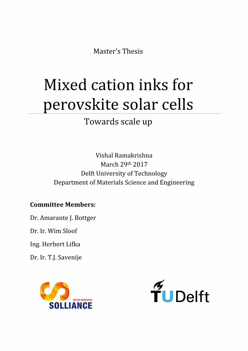
1. INTRODUCTION In the last few years, intensive investigations have been done to find a viable photovoltaic technology to match the power conversion efficiency and ubiquity of conventional Silicon based photovoltaics, while trying to lower the costs of production and installation. In this aspect, recent research in Perovskite Solar Cells (PSCs), which use organo-metal halide perovskites as an absorptive layer, have shown promising results in both power conversion efficiencies and lower processing costs[1]–[4]. First reported in 2009 by Kojima et al.[1], with a power conversion efficiency of 3.8%, they have shown rapid progress in the span of a few years[2] to reach efficiencies over 20%[3], [4]. This is due to the excellent light absorption, ideal band gap, high charge transport properties and chemical tunability it possesses.
This rapid progress, combined with fast energy investment returns[5] and a compatibility to two decades of research on their predecessors, the Dye-Sensitized Solar Cells (DSSCs) & Organic Photovoltaics (OPV) , make PSCs an ideal candidate for the next generation photovoltaic technologies. In addition, the low costs and simple processing techniques involved in their production makes them market-friendly.
Fig. 1: The NREL efficiency chart showing the current progress in efficiencies of PSCs. [6]
PROJECT AIM Despite the rapid growth of PSC technology, the properties of the organo-metal halide perovskites are still not understood. Recent research has looked into engineering the bandgap of the material by changing the cations, anions and the halides that make up the perovskite[4], [7]–[10]. However, changing composition in the solution, and its effect on the crystal growth and performance of the cells is still under study[10], [11]. In addition, research is on to meet the need for a safe, high efficiency, and stable ink for large scale roll-to-roll production[12]–[14].
This project deals with the crystallographic, performance and optimization study of mixed-cation perovskite inks for large scale PSC production. By coating these inks on the scale-up compatible planar, compact TiO2
layer, used as a selective electron transport layer, the crystallographic, optical,

6
and electrical properties of these inks were studied and compared to the Solliance baseline perovskite, a 45 wt.% solution of 1 M PbCl2/Pb(OAc)2 (1:4) + 3 M CH3NH3I in DMF.
Currently, the main inks used in PSC research are Methylammonium (MA)- (MAPbI3 was the first perovskite to be used for soar cell purposes) and Formamidinium (FA)- based perovskites, because of the ease at which their bandgaps can be tuned by changing their compositions. However, MA- based perovskites have been shown to be less than ideal for future scale up purposes due to their instability when exposed to even a little humidity in the atmosphere, and FA-perovskites are inherently unstable as the crystal structure prefers to relax into a non-perovskite phase after crystallisation (discussed further in the Theory section). This has paved way for research into hybrid perovskites[4], [7], [10], [15], [16], where the crystal structure is engineered by mixing the different cations to “arrest” the crystal structure in the active perovskite phase, and prevent it from phase-transforming into the inactive phase. Based on literature, two possible candidate inks were chosen: FA0.85MA0.15PbI2.5Br0.5
[7], [10] and the triple cation Cs0.05(FA0.85MA0.15)0.95PbI2.5Br0.5 [4], [17]. These inks were chosen due to the high stability and the performance they have exhibited. In fact, at the time of this project, the FA0.85MA0.15PbI2.5Br0.5 held the efficiency record among perovskite devices.
The first section of the reports deals with the nature and working principle of organo-metal halide perovskites and their use as absorber layers in solar cells. This understanding will then be used in realising the main objective of finding a suitable hybrid perovskite ink, which not only exhibits good performance and stability, but also scale-up compatibility.

7
2.BACKGROUND The following section entails a brief summary about perovskite solar cells and its characteristics. This background information delves into the literature associated to the technology and is necessary in order to understand how the crystallographic differences in perovskites affect their performance.
2.1 SOLAR ENERGY AND SOLAR CELLS The amount of sunlight reaching the earth, if converted to electricity, is more than capable of matching and surpassing humanity’s growing energy needs[18]. This conversion of sunlight to electricity can be achieved by using solar cells, a photovoltaic (PV) technology, that uses different semiconductor materials to absorb incoming photons and convert them to electricity through electron excitation. The most commonly used solar cell is a p-n junction of doped silicon, but as seen in Fig. 1, other new technologies are catching up to its performance standards.
Fig. 2: Band diagram of an n-i-p solar cell. [19]
In a p-i-n junction, electrons are usually found in the valence band, and are bound to other electrons in the valence band through various interactions. In order to be useful (i.e., to create electric current), these electrons must be excited to the high energy conduction band. This can be achieved by exposing the intrinsic layer to light. If the energy of the incoming photon is more than the band gap of the material, it can be absorbed and given to the electron, which then jumps into the conduction band, leaving behind a positively charged vacancy called a hole. The cell is engineered in such a way that this electron transition occurs only in one direction.
This electron is then collected via a conductor and passed through the load, while the holes in the valence band recombine with the electrons on the other end of the circuit, setting up an electric current.
The amount of incoming light energy that is converted to electrical energy determines the efficiency of the cell. By accounting for various losses, Shockley and Queisser showed that the theoretical maximum efficiency of a single junction solar cell is limited to ≈34%[20]. Current solar cell technologies have an average of 15-20% efficiencies.
2.2 THE PEROVSKITE CRYSTAL STRUCTURE AND ITS PROPERTIES The word “Perovskite” refers to a family of structural materials that shares the same crystal structure as calcium titanium oxide. The general structure is of the form ABX3 where A and B are cations (where the ionic radii of A>>B), and X is an anion that bonds to both the cations.

8
The ideal perovskite structure has a cubic Pm3m symmetry, with the A cation in the cube corner position (0, 0, 0), the B cation in the body centre (1/2, 1/2, 1/2) and the X anions at position (1/2, 1/2, 0). But the structure is slightly unstable against rotation with respect to the octahedral, and can thus undergo phase transformation[21]. The most common phases that the perovskites transform into are the orthorhombic and tetragonal phases.
Fig. 3: a) The Perovskite crystal unit cell, with the A, B and X ions represented by green, blue and red balls, respectively. b) phase shift of organo-metal halide perovskite from tetragonal to cubic phase. [11]
The crystallographic stability of perovskites can be represented by a tolerance factor, t and an octahedral factor, µ [22]. The factors t and µ are defined as
t =(Ra + 𝑅𝑥)
√2(𝑅𝑏 + 𝑅𝑥)
µ =𝑅𝑏
𝑅𝑥
where Ra, Rb and Rx are the ionic-radii of the A- cation, B- cation and the anion X respectively.
In organo-metal halides, A is generally an organic cation, like Methyl ammonium (MA/CH3NH3), B is the smaller metal cation, commonly Pb2+ and X are generally halide anions including Iodide (I-), Chloride (Cl-) and Bromide (Br-). For these halide perovskites ( X= Cl-, I-, Br-), generally 0.81 < t < 1.11 and 0.44 < μ < 0.90[22]. When t lies in the range of 0.89-1.0, the cubic perovskite structure is likely, with lower t values resulting in tetragonal and orthorhombic structures.
The desired phase is the photo-active cubic phase, which is typically much darker than the other phases, and is referred to as the “black” phase . But, single cation MA, FA or Cs perovskites readily degrade into non perovskite “yellow” phases[4], [7], [8], [23]. Transitions between the possible structures is very common, and can be bought about by changing the constituent ions, or by heating it at varying temperatures, with cubic structure more prevalent at high temperatures.
Fig. 4: The Perovskite crystal structure (a) and associated tolerance factors (b) [2].

9
The most commonly used organo-metal halide perovskite in literature is MAPbI3, which has been shown to exist in four temperature-dependent phases[24], [25], which are:
1. α phase: High temperature (>330K) pseudo-cubic phase with P4mm space group. This is because the MA+ ions prevent the formation of the cubic Pm3m.
2. β phase: room temperature tetragonal phase with I4/mcm space group. 3. γ phase: Low temperature (<161K) orthorhombic phase with Pnam space group. 4. δ phase: non perovskite-phase, due to the presence of solvent.
Further work shows that the high rotational freedom of MA+ ion in the lattice structure of the perovskite affects not only the structural properties of the perovskite, but also its bandgap.
The following table, taken from the work done by Poglitsch and Weber[26] shows the temperature dependent properties of MAPbX3 perovskite crystals
Fig. 5: Temperature dependent properties of MAPbX3. [26]
2.3 OPTICAL AND ELECTRICAL PROPERTIES OF PEROVSKITES Metalorganic halide perovskites have been shown to have excellent absorption properties, which means even a layer 500 nm thick can absorb most of the incoming photons. They also have a tunable bandgap between 1.5-2.3 eV[15], [17], [27], making them suitable for tandem applications.
They have also been shown to have excellent charge transport properties, capable of generating
voltages of up to 1.1 V[16], [25], [28], [29].
2.4 THE PEROVSKITE SOLAR CELL Just as the dye in DSSCs or intrinsic layers in p-i-n silicon cells, perovskite acts as the light absorbers in the PSC, and in addition, also act as charge generators . Their high absorption coefficient allows the perovskite to absorb a high number of photons for very small thicknesses (≈500nm), and high charge mobility and short circuit current densities (Jsc) can give large fill factors[30].
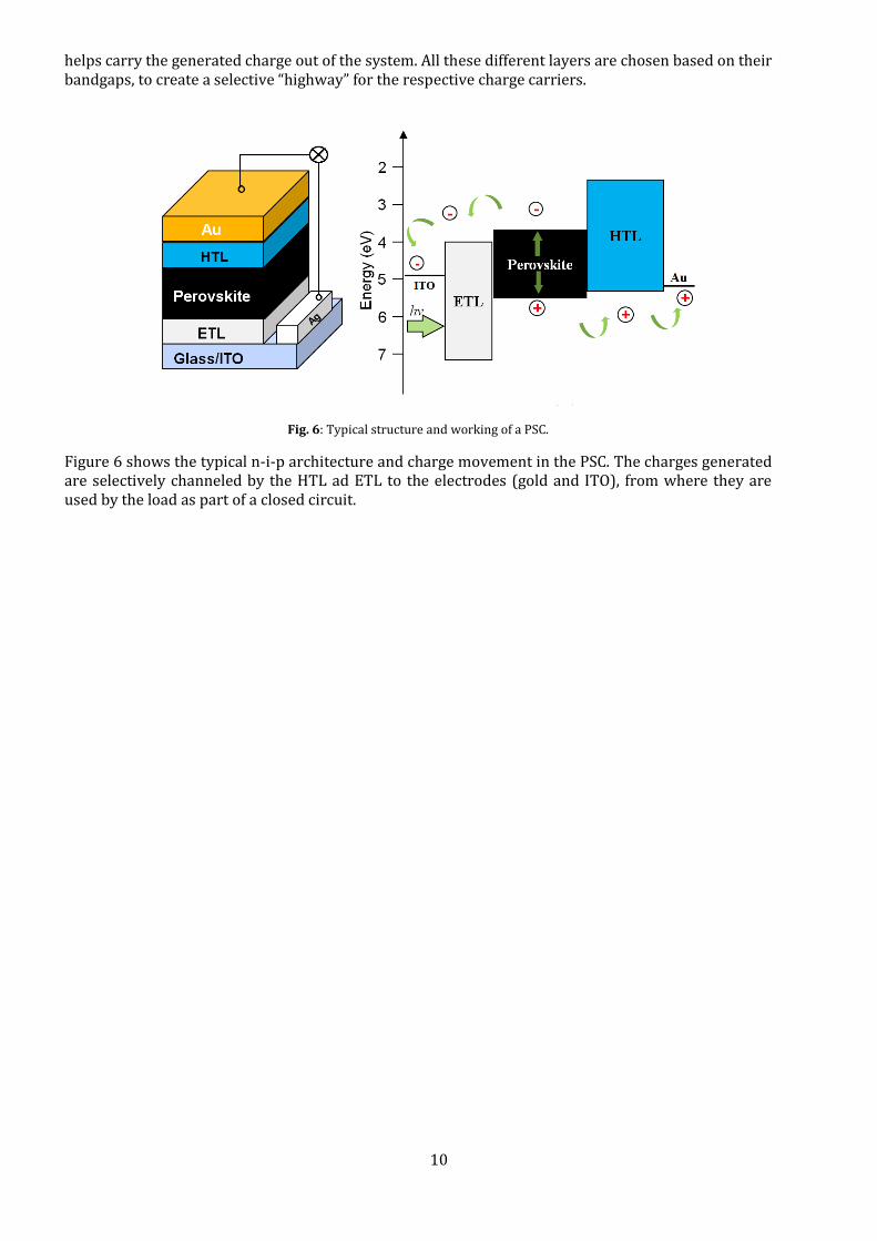
A perovskite solar cell acts as an intrinsic semiconductor, where a central active area produces an electron-hole pair when it absorbs an incoming photon. Unlike the doped n- and p-type regions of a typical Si-cell, the PSC consists of the perovskite sandwiched between an electron- and hole- transport layer (ETL and HTL), in an n-i-p or p-i-n structure. These in turn are in contact with electrodes that
10
helps carry the generated charge out of the system. All these different layers are chosen based on their bandgaps, to create a selective “highway” for the respective charge carriers.
Fig. 6: Typical structure and working of a PSC.
Figure 6 shows the typical n-i-p architecture and charge movement in the PSC. The charges generated are selectively channeled by the HTL ad ETL to the electrodes (gold and ITO), from where they are used by the load as part of a closed circuit.
11
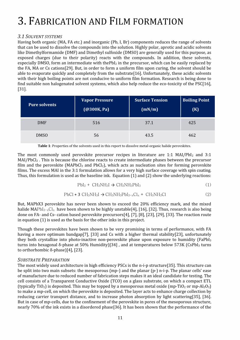
3. FABRICATION AND FILM FORMATION 3.1 SOLVENT SYSTEMS Having both organic (MA, FA etc.) and inorganic (Pb, I, Br) components reduces the range of solvents that can be used to dissolve the compounds into the solution. Highly polar, aprotic and acidic solvents like Dimethylformamide (DMF) and Dimethyl sulfoxide (DMSO) are generally used for this purpose, as exposed charges (due to their polarity) reacts with the compounds. In addition, these solvents, especially DMSO, form an intermediate with thePbI2 in the precursor, which can be easily replaced by the FA, MA or Cs cations[29]. But, in order to form a uniform film upon curing, the solvent should be able to evaporate quickly and completely from the substrate[16]. Unfortunately, these acidic solvents with their high boiling points are not conducive to uniform film formation. Research is being done to find suitable non halogenated solvent systems, which also help reduce the eco-toxicity of the PSC[16], [31].
Pure solvents Vapor Pressure
(@300K, Pa)
Surface Tension
(mN/m)
Boiling Point
(K)
DMF 516 37.1 425
DMSO 56 43.5 462
Table 1: Properties of the solvents used in this report to dissolve metal-organic halide perovskites.
The most commonly used perovskite precursor recipes in literature are 1:1 MAI/PbI2 and 3:1 MAI/PbCl2 . This is because the chlorine reacts to create intermediate phases between the precursor film and the perovskite (MAPbCl3 and PbCl2), which acts as nucleation sites for forming perovskite films. The excess MAI in the 3:1 formulation allows for a very high surface coverage with spin coating. Thus, this formulation is used as the baseline ink. Equation (1) and (2) show the underlying reactions:
PbI2 + CH3NH3I → CH3NH3PbI3 (1)
PbCl + 3 CH3NH3I → CH3NH3PbI3-xClx + CH3NH3Cl (2)
But, MAPbX3 perovskite has never been shown to exceed the 20% efficiency mark, and the mixed halide MAPbI3-xClx have been shown to be highly unstable[4], [16], [32]. Thus, research is also being done on FA- and Cs- cation based perovskite precursors[4], [7], [8], [23], [29], [33]. The reaction route in equation (1) is used as the basis for the other inks in this project.
Though these perovskites have been shown to be very promising in terms of performance, with FA having a more optimum bandgap[7], [33] and Cs with a higher thermal stability[23], unfortunately they both crystallize into photo-inactive non-perovskite phase upon exposure to humidity (FaPbI3 turns into hexagonal δ-phase at 50% Humidity)[34] , and at temperatures below 573K (CsPbI3 turns to orthorhombic δ-phase)[4], [23].
SUBSTRATE PREPARATION The most widely used architecture in high efficiency PSCs is the n-i-p structure[35]. This structure can be split into two main subsets: the mesoporous (mp-) and the planar (p-) n-i-p. The planar cells’ ease of manufacture due to reduced number of fabrication steps makes it an ideal candidate for testing. The cell consists of a Transparent Conductive Oxide (TCO) on a glass substrate, on which a compact ETL (typically TiO2) is deposited. This may be topped by a mesoporous metal oxide (mp-TiO2 or mp-Al2O3) to make a mp-cell, on which the perovskite is deposited. The layer acts to enhance charge collection by reducing carrier transport distance, and to increase photon absorption by light scattering[35], [36]. But in case of mp-cells, due to the confinement of the perovskite in pores of the mesoporous structure, nearly 70% of the ink exists in a disordered phase[36]. It has been shown that the performance of the
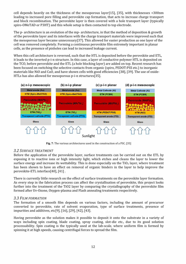
12
cell depends heavily on the thickness of the mesoporous layer[15], [35], with thicknesses <300nm leading to increased pore filling and perovskite cap formation, that acts to increase charge transport and block recombination. The perovskite layer is then covered with a hole transport layer (typically spiro-OMeTAD or P3HT) and this whole setup is then contacted to top electrode.
The p- architecture is an evolution of the mp- architecture, in that the method of deposition & growth of the perovskite layer and its interfaces with the charge transport materials were improved such that the mesoporous layer became unnecessary[37]. This allowed for easier production as one layer of the cell was removed completely. Forming a continuous perovskite film extremely important in planar cells, as the presence of pinholes can lead to increased leakage current.
When this cell architecture is reversed, such that the HTL is deposited before the perovskite and ETL, it leads to the inverted p-i-n structure. In this case, a layer of conductive polymer HTL is deposited on the TCO, before perovskite and the ETL (a hole blocking layer) are added on top. Recent research has been focused on switching the selective contacts from organic (spiro, PEDOT:PSS etc.) to inorganic materials like NiO and CuO, and have shown cells with good efficiencies [38], [39]. The use of oxide-HTLs has also allowed for mesoporous p-i-n structures[35].
Fig. 7: The various architectures used in the construction of a PSC. [35]
3.2 SURFACE TREATMENT Before the application of the perovskite layer, surface treatments can be carried out on the ETL by exposing it to reactive ions or high intensity light, which etches and cleans the layer to lower the surface energy and increase its wettability. This is done especially on the TiO2 layer, where treatment has been shown to have an effect on removal of organic binders in the layer to help improve the perovskite-ETL interface[40], [41] .
There is currently little research on the effect of surface treatments on the perovskite layer formation. As every step in the fabrication process can affect the crystallisation of perovskite, this project looks further into the treatment of the TiO2 layer by comparing the crystallography of the perovskite film formed after Uv-Ozone, Oxygen-plasma and Flash annealing treatments respectively.
3.3 FILM FORMATION The formation of a smooth film depends on various factors, including the amount of precursor converted to perovskite, rate of solvent evaporation, type of surface treatments, presence of impurities and additives, etc[9], [16], [29], [42], [43].
Having perovskite as the solution makes it possible to deposit it onto the substrate in a variety of ways including spin coating, blade coating, spray coating, slot-die etc., due to its good solution processability. Spin coating is the typically used at the lab-scale, where uniform film is formed by spinning it at high speeds, causing centrifugal forces to spread the film.
13
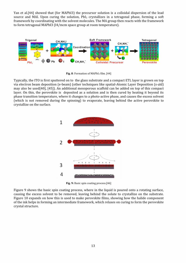
Yan et al.[44] showed that (for MAPbI3) the precursor solution is a colloidal dispersion of the lead source and MAI. Upon curing the solution, PbI2 crystallizes in a tetragonal phase, forming a soft framework by coordinating with the solvent molecules. The MA group then reacts with the framework to form tetragonal MAPbI3 (I4/mcm space group at room temperature).
Fig. 8: Formation of MAPbI3 film. [44]
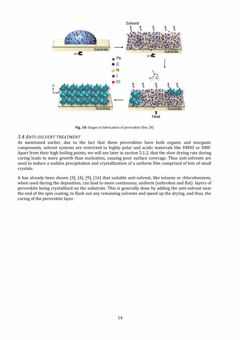
Typically, the ITO is first sputtered on to the glass substrate and a compact ETL layer is grown on top via electron beam deposition (e-beam) (other techniques like spatial-Atomic Layer Deposition (s-ald) may also be used[40], [45]). An additional mesoporous scaffold can be added on top of this compact layer. On this, the perovskite is deposited as a solution and is then cured by heating it beyond its phase transition temperature, where it changes to a photo-active phase, and causes the excess solvent (which is not removed during the spinning) to evaporate, leaving behind the active perovskite to crystallize on the surface.
Fig. 9: Basic spin coating process.[46]
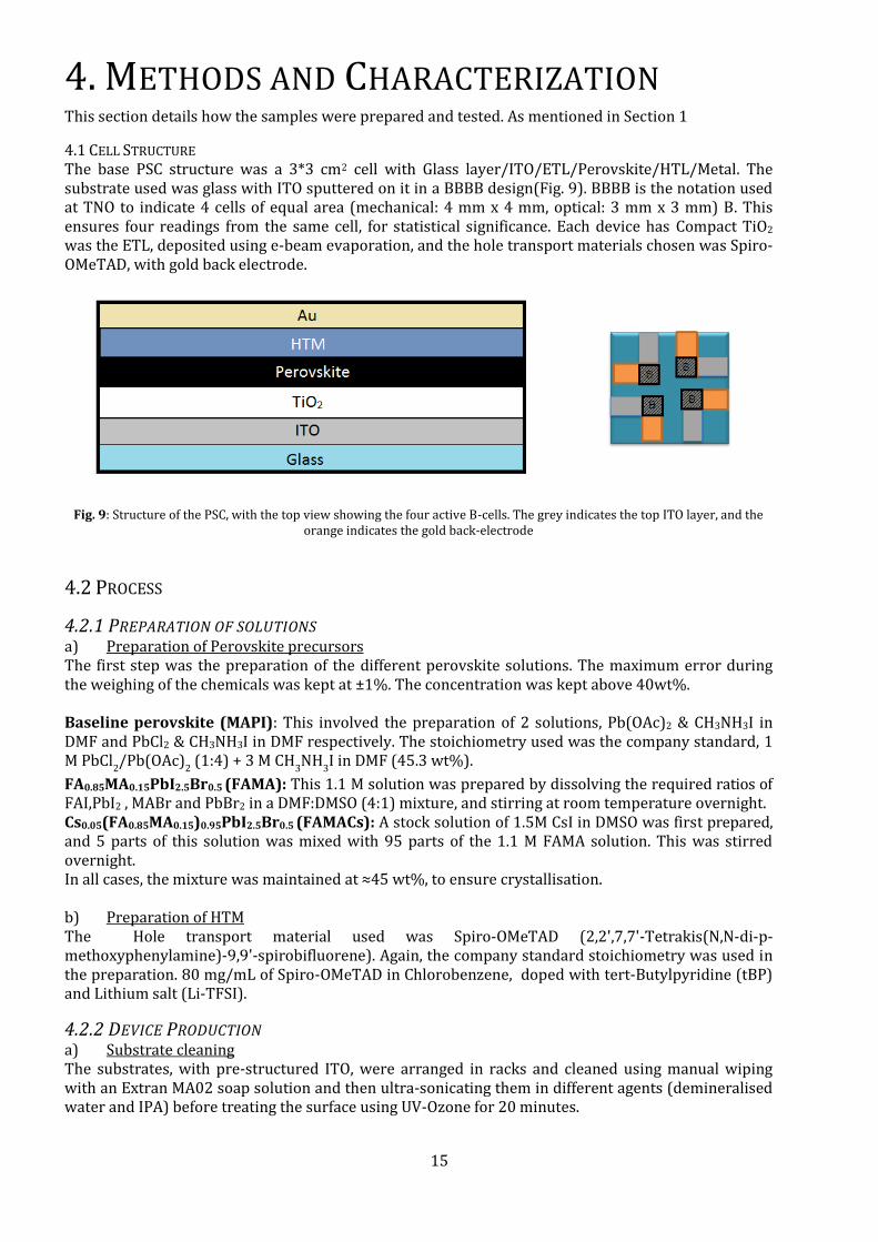
Figure 9 shows the basic spin coating process, where in the liquid is poured onto a rotating surface, causing the excess solvent to be removed, leaving behind the solute to crystallize on the substrate. Figure 10 expands on how this is used to make perovskite films, showing how the halide component of the ink helps in forming an intermediate framework, which relaxes on curing to form the perovskite crystal structure.
14
Fig. 10: Stages in fabrication of perovskite film. [8]
3.4 ANTI-SOLVENT TREATMENT As mentioned earlier, due to the fact that these perovskites have both organic and inorganic components, solvent systems are restricted to highly polar and acidic materials like DMSO or DMF. Apart from their high boiling points, we will see later in section 5.1.2, that the slow drying rate during curing leads to more growth than nucleation, causing poor surface coverage. Thus anti-solvents are used to induce a sudden precipitation and crystallization of a uniform film comprised of lots of small crystals.
It has already been shown [3], [4], [9], [16] that suitable anti-solvent, like toluene or chlorobenzene, when used during the deposition, can lead to more continuous, uniform (unbroken and flat) layers of perovskite being crystallized on the substrate. This is generally done by adding the anti-solvent near the end of the spin coating, to flush out any remaining solvents and speed up the drying, and thus, the curing of the perovskite layer.
15
4. METHODS AND CHARACTERIZATION This section details how the samples were prepared and tested. As mentioned in Section 1
4.1 CELL STRUCTURE The base PSC structure was a 3*3 cm2 cell with Glass layer/ITO/ETL/Perovskite/HTL/Metal. The substrate used was glass with ITO sputtered on it in a BBBB design(Fig. 9). BBBB is the notation used at TNO to indicate 4 cells of equal area (mechanical: 4 mm x 4 mm, optical: 3 mm x 3 mm) B. This ensures four readings from the same cell, for statistical significance. Each device has Compact TiO2 was the ETL, deposited using e-beam evaporation, and the hole transport materials chosen was Spiro-OMeTAD, with gold back electrode.
Fig. 9: Structure of the PSC, with the top view showing the four active B-cells. The grey indicates the top ITO layer, and the
orange indicates the gold back-electrode
4.2 PROCESS
4.2.1 PREPARATION OF SOLUTIONS a) Preparation of Perovskite precursors The first step was the preparation of the different perovskite solutions. The maximum error during the weighing of the chemicals was kept at ±1%. The concentration was kept above 40wt%. Baseline perovskite (MAPI): This involved the preparation of 2 solutions, Pb(OAc)2 & CH3NH3I in DMF and PbCl2 & CH3NH3I in DMF respectively. The stoichiometry used was the company standard, 1 M PbCl
2/Pb(OAc)
2 (1:4) + 3 M CH
3NH
3I in DMF (45.3 wt%).
FA0.85MA0.15PbI2.5Br0.5 (FAMA): This 1.1 M solution was prepared by dissolving the required ratios of FAI,PbI2 , MABr and PbBr2 in a DMF:DMSO (4:1) mixture, and stirring at room temperature overnight. Cs0.05(FA0.85MA0.15)0.95PbI2.5Br0.5 (FAMACs): A stock solution of 1.5M CsI in DMSO was first prepared, and 5 parts of this solution was mixed with 95 parts of the 1.1 M FAMA solution. This was stirred overnight. In all cases, the mixture was maintained at ≈45 wt%, to ensure crystallisation. b) Preparation of HTM The Hole transport material used was Spiro-OMeTAD (2,2',7,7'-Tetrakis(N,N-di-p-methoxyphenylamine)-9,9'-spirobifluorene). Again, the company standard stoichiometry was used in the preparation. 80 mg/mL of Spiro-OMeTAD in Chlorobenzene, doped with tert-Butylpyridine (tBP) and Lithium salt (Li-TFSI).
4.2.2 DEVICE PRODUCTION a) Substrate cleaning The substrates, with pre-structured ITO, were arranged in racks and cleaned using manual wiping with an Extran MA02 soap solution and then ultra-sonicating them in different agents (demineralised water and IPA) before treating the surface using UV-Ozone for 20 minutes.

16
b) TiO2 Deposition An e-beam evaporator (Scotty Cryofox™) was used to deposit 50nm of TiO2 on the samples, at a rate of 0.1 nm/s under vacuum. For mesoporous-TiO2 (mp-TiO2), a dispersion of TiO2 nano particles in water and ethanol (provided by Solaronix SA) was spin coated onto the planar TiO2 surface at 900 rpm for 60 s (@930 rpm/s) and then cured at 413K for 10 minutes. c) Curing the Electron transport layer The TiO2 layer, which acted as the electron transport layer (ETL) was then treated with 20 minutes of ultraviolet radiation under Ozone atmosphere (in a Uvikon PR-100 reactor) to help reduce the surface energy for even spread and uniform growth of perovskite film grown on top. For the experiments involving different surface treatments, Oxygen plasma (in a Branson IPC P2100) and Flash sintering (in a Novacentric Pulseforge 1300 flash sintering tool) were used. The flash sintering involved exposing the surface to 10 Flashes of high intensity light at an energy flux of 6.6 J cm-2. d) Spin coating of Perovskite solution The samples were then transferred to a clean glovebox, for the spin coating process. The speed and acceleration of the spin coater was selected for the perovskite solution from the pre-programmed list. The substrate was held at the center of the spin coater and was held in place by vacuum. The surface of the substrate was cleaned using nitrogen. In the case of baseline perovskite, 60 µL of perovskite solution was deposited on the substrate after the start of spinning (5000 rpm for 60 s @1000rpm/s). For the anti-solvent process in case of FAMA- and FAMACs- perovskites, the solution was first deposited at the middle of the sample before the spinning was started (static dispense), and the spinning was done in two stages: one to spread the solution evenly (1000 rpm/s for 20 s @500rpm/s) and then the coating stage ( 5000 rpm for 40 s @5000rpm/s). The required amount of anti-solvent was deposited 10 seconds before the end of the coating stage. e) Curing of Perovskite The substrates were then placed on the hot plate, depending on the experiment. Ramp: The plate was set at 363 K and then the power was increased such that temperature ramps to 403 K in 5 minutes. The samples were then cured for 10 minutes, and moved back to the sample holders. Isothermal: The plate was set at the required temperature (383 K or 403K) and the samples were placed directly on the plate and treated for the required amount of time.
Fig. 10: Different curing routes used
In case a working device was being made (for measurement of electrical characteristics), the samples were cured at 403K for 10 minutes and the following steps were done to complete the device:
17
f) Spin coating of HTL solutions Each sample was then spin coated with the spiro-OMeTAD dried for a minute. They were then placed in a humid environment (≈30% RH) overnight. This "air-soaking" phase was found to be necessary for the spiro in order to get high performances from the working devices. g) Wiping of sample edges The sample edges were then carefully wiped with a 6:1 solution of chlorobenzene in DMF, to remove any excess solution that had flowed out of the active area during spin coating. This was done to prevent the development of any contact between the gold and ITO during the evaporation process. h) Deposition of Au electrodes Samples were then loaded onto an evaporator for deposition of the gold electrode. A mask was used to coat only the active areas of the device. The evaporator was programmed to deposit 100nm of gold at a rate of 0.1 nm/s in a vacuum of 1*10-6 mbar pressure.
4.3 CHARACTERIZATION OF SAMPLES AND DEVICES
4.3.1 XRD The samples (without HTL/back electrodes) were mounted onto a Phillips X'Pert SR5068 powder diffractometer, to determine the crystallographic structure of the perovskites at various cure temperatures. The diffractometer is equipped with a Cu- Kα source (with Kα1 & Kα2 wavelengths of 1.540598 nm and 1.544426 nm respectively), and was programmed to do a continuous scan between 2θ=5° to 2θ=65°. For air-sensitive perovskites, a PET barrier film was used to prevent exposure of the surface to air. This PET film gave a strong, broad peak at 2θ≈26°. The peaks were then matched to the corresponding spectra from literature, and the hkl values were used with the lattice spacing d from Bragg’s law,
𝑛. 𝜆 = 2𝑑ℎ𝑘𝑙 𝑠𝑖𝑛𝜃 With the formula for Interplanar spacing,
For cubic phase: 1
𝑑2 =ℎ2+𝑘2+𝑙2
𝑎2
For tetragonal phase: 1
𝑑2 =ℎ2+𝑘2
𝑎2 +𝑙2
𝑐2
To find the lattice constants a and c of the phases. Since the photo active cubic phase is of interest, the first spacing formula was used mainly.
4.3.2 SEM Scanning electron microscopy was performed on the samples using a JEOL JSM-6010LA Intouchscope™. In case of samples that were sensitive to air, a 5 nm thick layer of gold was deposited on top of the perovskite to prevent degradation of samples while loading.
4.3.3 UV-VISIBLE SPECTROSCOPY An Agilent/HP 8453 UV-Visible spectrophotometer was used to measure the transmission spectra of the perovskites. Except for the baseline perovskite films, which had a thickness of ≈450 nm, the thickness of the films formed using the other two inks were found using a Bruker™ Dektak XT contact profilometer.
Reference measurements were taken with only ITO/TiO2 layers (and PET film, where used) to compare the transmission properties of the perovskite films.
(4.1)
(4.2)
(4.3)

18
As the equipment itself is an open air, quick-measure system, it did not have an integration sphere. the measure of absorption spectra could not be done (due to unwanted scatter and external light sources), thus the direct transmission spectra was measured and the absorption coefficient calculated from the measurements. By comparing the slope steepness, the speed of transition from blocking to transmission could be estimated and compared.
The absorption coefficient can be found from transmission spectra by using Beer-Lambert’s law
𝐴 = 𝑙𝑜𝑔10(%𝑇)
𝑎 =ln
%𝑇
100
𝑑
Where A is the amount of light absorbed and %T is the percentage transmission and d is the measured thickness of film.
To find the approximate band gaps, a Tauc plot was plotted. This plot obeys the condition that the absorption coefficient a obeys the equation
(𝑎ℎ𝜈) 𝛼 (ℎ𝜈 − 𝐸𝑔𝑎𝑝)𝑛
Where a is the absorption coefficient, ν is the wavenumber and n= 1, 1/2, 2 or 3/2 depending on the type of bandgap, and h is Planck’s constant. By plotting (ahν)1/n vs hν, we can find the intercept drawn at the band edge to find the approximate bandgap.
4.3.4 MINI SUN SIMULATOR An in-house sun simulator was used as a JV measurement setup for 3x3 cm2 devices, to measure the electrical characteristics of the working devices.
Before testing the devices, the contacts were setup by coating the electrodes with a layer of silver paint. The Sun simulator was then switched on and the voltage of the lamp was set to simulate 1 sun (1000 W/m2, 1.5AM) conditions. The mask selected for the test is a BBBB mask, with 4 cells of area 0.089 cm2.
Fig. 10: The mask cells and their designations.
The simulator was then calibrated for the cell using a silicon reference cell with a known spectral response, and the samples were then tested for their JV and Maximum Power Point (MPP) characteristics.
Performance parameters
The open circuit voltage (VOC), short circuit current (JSC) and fill factor (ratio of maximum power generated by device to the theoretical power) was measured for the devices in both forward and
The etching on the rear was considered the “up” of the sample, and it was slid into the sample holder of the sun simulator in this direction, glass on top, light source beaming down on it.
(4.3)
(4.4)
(4.5)
19
reverse bias. The cells were measured after 2 minutes of light-soaking to ensure activation of the perovskite layer.
From this, the power conversion efficiency (%PCE) of the devices were measured. %PCE can be expressed as:
%𝑃𝐶𝐸 =𝑃𝑜𝑢𝑡
𝑃𝑖𝑛=
𝐽𝑆𝐶.𝑉𝑂𝐶.𝐹𝐹
𝑃𝑖𝑛
Where Pout and Pin are the power output and light power input respectively.
JV curves
The current density-voltage characteristics were plotted for the sample exposed to the light, between the Voltage range of -1.2 to 1 V, with a step size of 0.01V and scan rate of 300V/s at the maximum measure speed of the setup. The setup itself consisted of a four probe connection, that reduced the sensitivity to any losses during measurement.
The sample was then soaked in the light for 2 minutes and tested again. The light soaking showed an improved performance for the sample.
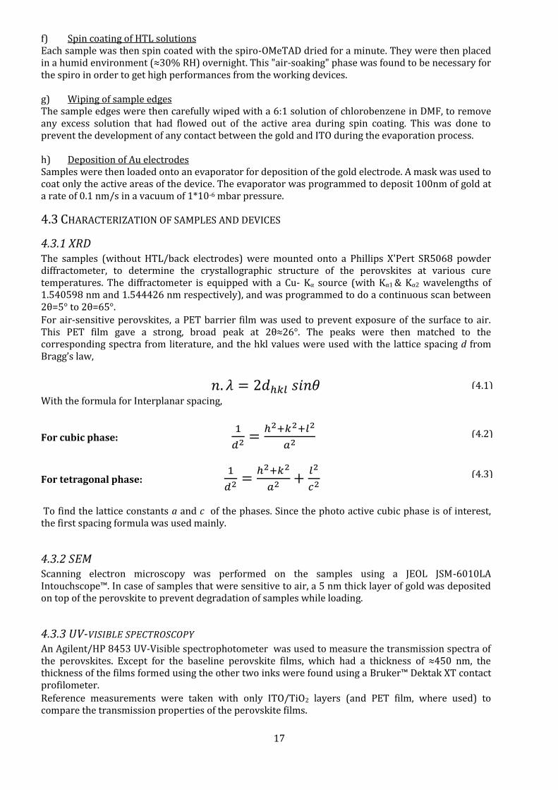
From the JV curves, the maximum power voltage (VMP) and current (JMP) can be observed and the characteristic and series resistances of the devices can be measured:
Fig. 11: (Left) Example JV curves and the corresponding voltage and current values (From:
http://www.pveducation.org/pvcdrom/characteristic-resistance) (note: here I is used for current, and is the same as J).(Right) Calculating the series resistances
The characteristic resistance gives the resistance of the cell at the its maximum power point and can be used as a measure of parasitic losses in the cell. From [47], we can estimate it as:
𝑅𝐶𝐻 =𝑉𝑀𝑃
𝐽𝑀𝑃≈
𝑉𝑂𝐶
𝐽𝑆𝐶
The series resistance of the cell is a measure of the various contact resistances between the layers of the cell, and can be calculated by taking the inverse of the slope of the JV curve at zero voltage. Maximum Power Point (MPP) curves
This involves digitally tracking the output of the devices and comparing it to the voltage required by a load cell. By continuously tracking the current voltage characteristics of the device and plotting the maximum power output, the variation in the efficiency of the cell can be tracked.
the stabilized maximum power point measurement was carried out on that cell area of the sample showing the best efficiency and VOC in the (post light soaking) JV test. The test was run for 5 minutes to determine the MPP, and therefore, VMPP and the JMPP. From this, the change in the power conversion efficiency over time was plotted.
(4.6)
(4.7)

20
5. RESULTS & DISCUSSIONS 5.1 CRYSTALLOGRAPHY AND MORPHOLOGY OF THE PEROVSKITES This section delves into the results of the X-Ray diffraction and Scanning Electron Microscopy (SEM) data obtained for the different perovskites. An analysis is done on each of the perovskite inks (Baseline, FAMA and FAMACs), and the differences between them were observed and compared
5.1.1 BASELINE PEROVSKITE- MAPI During the ramp curing of the baseline perovskites, the growth of the perovskite film undergoes two stages: first the loss of precursors, and second the growth of films.
The loss of precursors involves the reduction of precursor materials, and their conversion into the perovskite phase. As the temperature increases, the presence of lead iodide and intermediates diminish, and perovskite crystals are formed. In Fig. 12, we can see that upon simple drying (0 deg- no heat treatment yet), formation of intermediate phase occurs. This intermediate phase is then converted to tetragonal perovskite upon curing, shown by the black arrows, and at 383 K (110 deg), two different peaks are observed. This transformation appears to be rapid, happening within a 10°C rise in temperature.
Fig. 12: XRD pattern at different points in ramp curing of MAPI perovskite, 0 deg being no curing, 100-120 deg indicating
cure in the ramp stage from 373K to 393K, and 130 deg-s ,m &e standing for the start, middle and end of the plateau stage at 403 K. The Black arrows show the change in the intermediate phase.

21
In fig. 12, the spectra shows range from start of ramp 273K (0 deg) to the start(130 deg-s), after 5 minutes (130 deg-m), and after 10 min (130 deg-e) of plateau stage of ramp curing at 403 K. Due to the presence of large PET peaks and variation in the peak height, it is necessary to zoom into particular 2θ ranges to see the peaks. From literature, the peaks can be identified, and the lattice parameter of the structure formed can be calculated.
Fig. 13: XRD pattern of MAPI-cl perovskite formed at various temperatures during ramp curing. The subscript T and C stand for tetragonal- and cubic- phase respectively. The # shows the peaks for intermediates formed during curing. The arrow indicates the
direction in which peaks shift with increasing cure temperature. (Note: in order to clearly see the peaks, the y-axis (counts/intensity) is varied)
Comparing the peaks with the acetate based MAPI XRD pattern in Fig. 14 (from [9]), we can index
them and find any odd peaks. As can be seen in Fig. 13, the baseline perovskite forms crystals
primarily in the {001} and {110} tetragonal orientation. As the cure time increases, the tetragonal
crystals decrease in number, with the {001} crystals nearly disappearing. At higher 2θ angles (> 42°),
the growth of the {100} cubic system can be seen with increase in temperature. A peak shift can be
seen from 273 K and 373 K to 393 K and above.
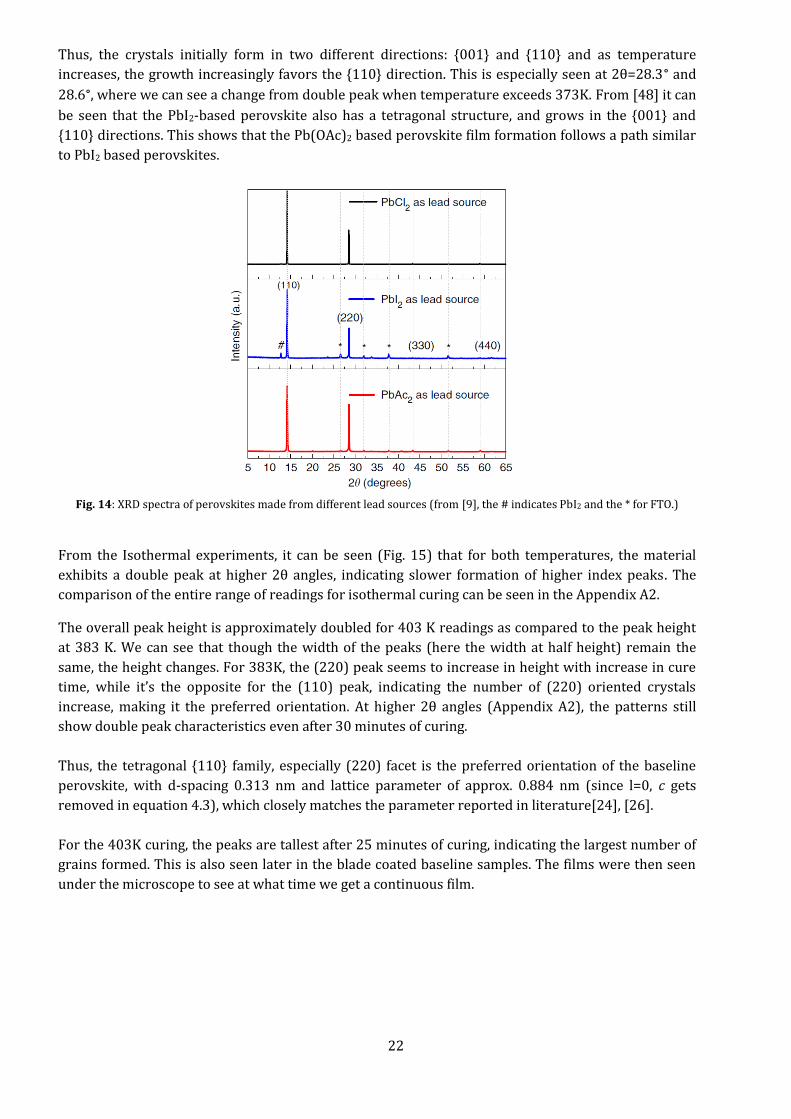
22
Thus, the crystals initially form in two different directions: {001} and {110} and as temperature
increases, the growth increasingly favors the {110} direction. This is especially seen at 2θ=28.3° and
28.6°, where we can see a change from double peak when temperature exceeds 373K. From [48] it can
be seen that the PbI2-based perovskite also has a tetragonal structure, and grows in the {001} and
{110} directions. This shows that the Pb(OAc)2 based perovskite film formation follows a path similar
to PbI2 based perovskites.
Fig. 14: XRD spectra of perovskites made from different lead sources (from [9], the # indicates PbI2 and the * for FTO.)
From the Isothermal experiments, it can be seen (Fig. 15) that for both temperatures, the material
exhibits a double peak at higher 2θ angles, indicating slower formation of higher index peaks. The
comparison of the entire range of readings for isothermal curing can be seen in the Appendix A2.
The overall peak height is approximately doubled for 403 K readings as compared to the peak height
at 383 K. We can see that though the width of the peaks (here the width at half height) remain the
same, the height changes. For 383K, the (220) peak seems to increase in height with increase in cure
time, while it’s the opposite for the (110) peak, indicating the number of (220) oriented crystals
increase, making it the preferred orientation. At higher 2θ angles (Appendix A2), the patterns still
show double peak characteristics even after 30 minutes of curing.
Thus, the tetragonal {110} family, especially (220) facet is the preferred orientation of the baseline
perovskite, with d-spacing 0.313 nm and lattice parameter of approx. 0.884 nm (since l=0, c gets
removed in equation 4.3), which closely matches the parameter reported in literature[24], [26].
For the 403K curing, the peaks are tallest after 25 minutes of curing, indicating the largest number of
grains formed. This is also seen later in the blade coated baseline samples. The films were then seen
under the microscope to see at what time we get a continuous film.

23
Fig. 15: XRD patterns of the baseline perovskite at different time intervals for isothermal curing at (Top) 383 K and
(Bottom) 403 K. The arrow indicates the direction in which peaks shift with increasing cure temperature.
Scanning electron microscopy (SEM) images (Fig. 16) show that it takes more than 15 minutes of
curing at 383 K to form a uniform, pinhole-free film. This takes less time when curing at 403 K. In both
cases, over-curing can lead to formation of pinholes again. This can be seen in the images for 30
minute treatment at both isothermal curing temperatures. This can be seen in the XRD patterns,
where we see a decrease in the (110) peak at 2θ=14.2° for both curing temperatures, treatment as
time increases. For 383K this is after the 20 minute mark(pink line), and for 403K after the 15 minute
mark (light blue line). The sudden increase in grains at the 25 minute mark is a curious effect, that is
also seen in blade coating experiments (Appendix A6).
As seen previously, for 403 K, though the largest number of grains seem to be formed at 25 minutes of
curing, the film itself contains pinholes.
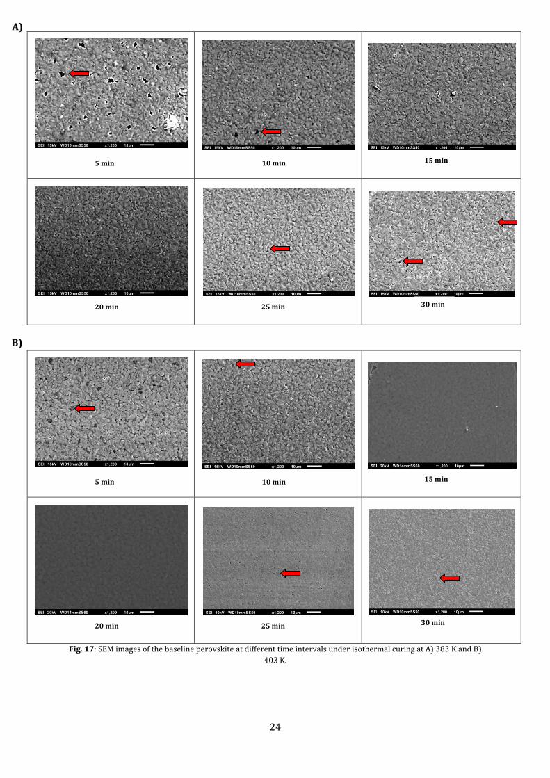
24
Fig. 17: SEM images of the baseline perovskite at different time intervals under isothermal curing at A) 383 K and B)
403 K.
5 min 10 min 15 min
20 min 25 min 30 min
5 min 10 min 15 min
20 min 25 min 30 min
A)
B)
25
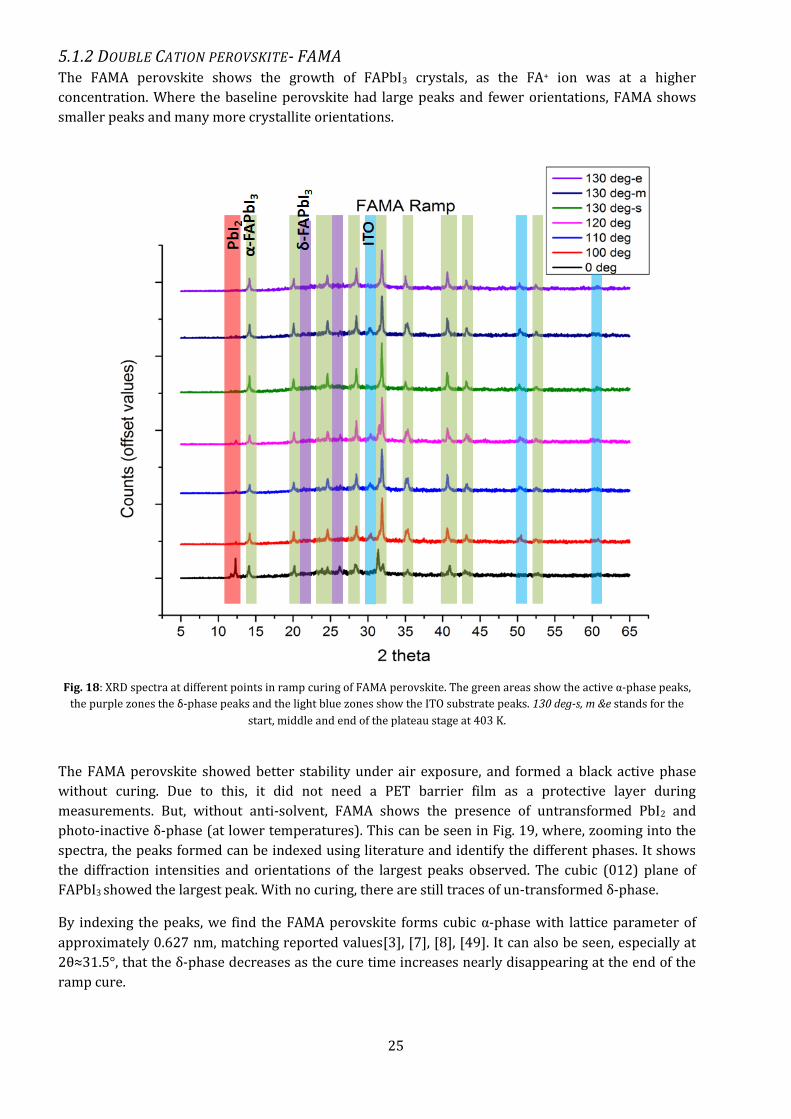
5.1.2 DOUBLE CATION PEROVSKITE- FAMA The FAMA perovskite shows the growth of FAPbI3 crystals, as the FA+ ion was at a higher
concentration. Where the baseline perovskite had large peaks and fewer orientations, FAMA shows
smaller peaks and many more crystallite orientations.
Fig. 18: XRD spectra at different points in ramp curing of FAMA perovskite. The green areas show the active α-phase peaks,
the purple zones the δ-phase peaks and the light blue zones show the ITO substrate peaks. 130 deg-s, m &e stands for the
start, middle and end of the plateau stage at 403 K.
The FAMA perovskite showed better stability under air exposure, and formed a black active phase
without curing. Due to this, it did not need a PET barrier film as a protective layer during
measurements. But, without anti-solvent, FAMA shows the presence of untransformed PbI2 and
photo-inactive δ-phase (at lower temperatures). This can be seen in Fig. 19, where, zooming into the
spectra, the peaks formed can be indexed using literature and identify the different phases. It shows
the diffraction intensities and orientations of the largest peaks observed. The cubic (012) plane of
FAPbI3 showed the largest peak. With no curing, there are still traces of un-transformed δ-phase.
By indexing the peaks, we find the FAMA perovskite forms cubic α-phase with lattice parameter of
approximately 0.627 nm, matching reported values[3], [7], [8], [49]. It can also be seen, especially at
2θ≈31.5°, that the δ-phase decreases as the cure time increases nearly disappearing at the end of the
ramp cure.
26
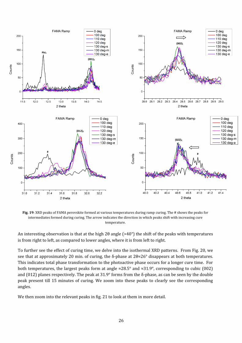
Fig. 19: XRD peaks of FAMA perovskite formed at various temperatures during ramp curing. The # shows the peaks for
intermediates formed during curing. The arrow indicates the direction in which peaks shift with increasing cure
temperature.
An interesting observation is that at the high 2θ angle (>40°) the shift of the peaks with temperatures
is from right to left, as compared to lower angles, where it is from left to right.
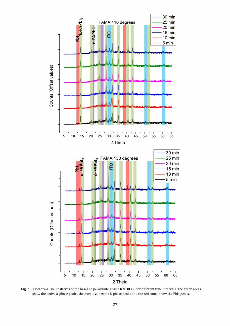
To further see the effect of curing time, we delve into the isothermal XRD patterns. From Fig. 20, we
see that at approximately 20 min. of curing, the δ-phase at 2θ≈26° disappears at both temperatures.
This indicates total phase transformation to the photoactive phase occurs for a longer cure time. For
both temperatures, the largest peaks form at angle ≈28.5° and ≈31.9°, corresponding to cubic (002)
and (012) planes respectively. The peak at 31.9° forms from the δ-phase, as can be seen by the double
peak present till 15 minutes of curing. We zoom into these peaks to clearly see the corresponding
angles.
We then zoom into the relevant peaks in fig. 21 to look at them in more detail.
27
Fig. 20: Isothermal XRD patterns of the baseline perovskite at 403 K & 383 K, for different time intervals. The green areas
show the active α-phase peaks, the purple zones the δ-phase peaks and the red zones show the PbI2 peaks.

28
Fig. 21: XRD patterns of the FAMA perovskite at different time intervals for isothermal curing at (Top) 383 K and (Bottom)
403 K. The arrow indicates the direction in which peaks shift with increasing cure temperature
From Fig. 21, it can be seen that for the curing at 403 K, the peak intensity decreases with cure time.
This indicates a cut-off time for the curing to have the best effect. The largest peaks form at 15-20
minutes of curing, and the angles correspond to a lattice parameter of ≈0.627 nm.
The morphology of these films shows (Fig. 22) large, leaf-like, circular islands with large gaps in
between, at both 383 K and 403 K curing. These islands eventually close up and coalesce at higher
curing temperature. This seems to follow the Volmer- Weber growth modes of thin films, where the
surface energy of the substrate is larger than the combined surface energies of the film-substrate
interface and the film formed, i.e., the atoms within the precursor droplets interact more strongly
with each other than with the substrate. Usually, this can be countered by increasing the thermal
energy given to the film, and that is why we see them coalesce after around 15 minutes of curing at
403 K. This might be due to the slow evaporation of the solvent in the precursor, causing the surface
energy to rise within the droplets. As can be seen in the SEM images, a lot of nucleation sites appear,
but little growth occurs. Later (section 5.2), we will see that this also caused these perovskites
devices to perform poorly, with high transmission of light. In literature, highly acidic HI was added
29
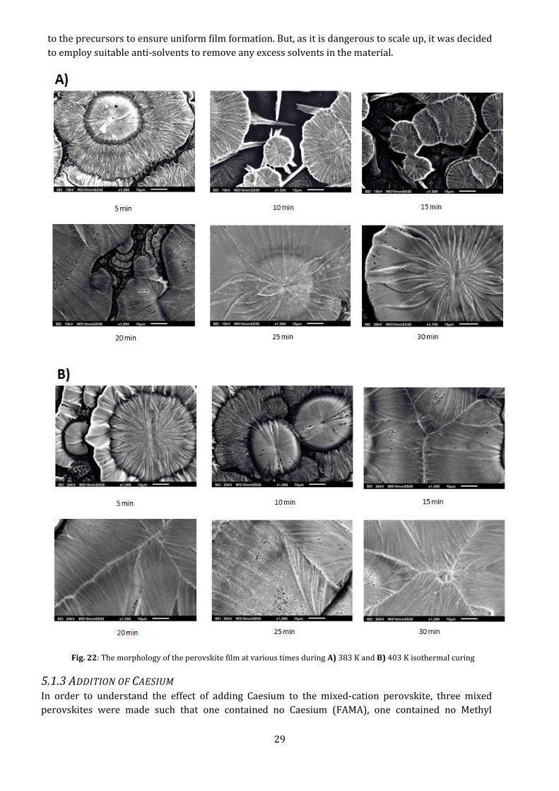
to the precursors to ensure uniform film formation. But, as it is dangerous to scale up, it was decided
to employ suitable anti-solvents to remove any excess solvents in the material.
Fig. 22: The morphology of the perovskite film at various times during A) 383 K and B) 403 K isothermal curing
5.1.3 ADDITION OF CAESIUM In order to understand the effect of adding Caesium to the mixed-cation perovskite, three mixed
perovskites were made such that one contained no Caesium (FAMA), one contained no Methyl

30
Ammonium (FACs) and one contained all three cations(FAMACs). Formamidinium was fixed as the
base cation, as FAPbI3 has the optimum bandgap of 1.5 eV[7], [17] (pure FAPbI3 perovskite itself is
very unstable, and tends to degrade to an inactive yellow phase post curing). These three perovskites
were then ramp cured for 10 minutes and compared.
Fig. 23: XRD spectra of the perovskites with varying cations, showing shift in peaks. The green areas show the active
α-phase peaks, the purple zones the δ-phase peaks, the red zones PbI2, and the light blue zones show the ITO
substrate peaks.
As can be seen from Fig. 21 , the Cs+ ion shifts the peaks to the right, decreasing the lattice size of the
(002) peak from 0.6265 nm (for the FAMA perovskite) and 0.625 nm (for the triple cation (FAMACs)
perovskite) to 0.6147 nm (for the FACs perovskite). Also, the FACs mix was the only one to present
traces of PbI2 still in it, showing that the addition of MA+ ion increases the conversion of the lead
iodide in the precursor film to active perovskite.
Due to its small size, the Cs+ ion effectively “arrests” the formation of FAPbI3 in the photo-active black
phase. The MA+ ion also has a similar effect, but appears to be slower, as can be seen by comparing
peaks at 28.5°, showing that while FAMA has a large number of small grains (greater peak height), the
FAMACs perovskite has small number of large grains (greater peak width). This is seen under the SEM
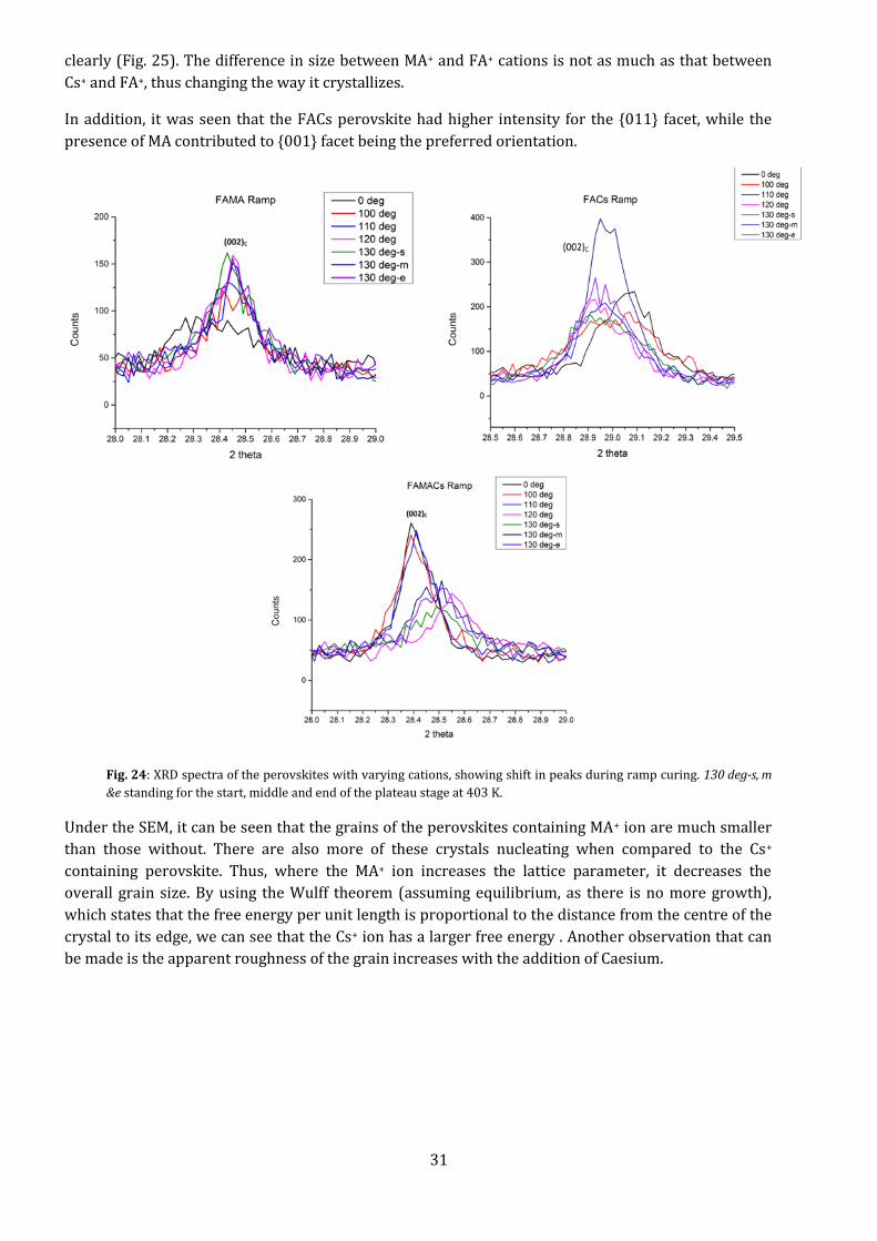
31
clearly (Fig. 25). The difference in size between MA+ and FA+ cations is not as much as that between
Cs+ and FA+, thus changing the way it crystallizes.
In addition, it was seen that the FACs perovskite had higher intensity for the {011} facet, while the
presence of MA contributed to {001} facet being the preferred orientation.
Fig. 24: XRD spectra of the perovskites with varying cations, showing shift in peaks during ramp curing. 130 deg-s, m
&e standing for the start, middle and end of the plateau stage at 403 K.
Under the SEM, it can be seen that the grains of the perovskites containing MA+ ion are much smaller
than those without. There are also more of these crystals nucleating when compared to the Cs+
containing perovskite. Thus, where the MA+ ion increases the lattice parameter, it decreases the
overall grain size. By using the Wulff theorem (assuming equilibrium, as there is no more growth),
which states that the free energy per unit length is proportional to the distance from the centre of the
crystal to its edge, we can see that the Cs+ ion has a larger free energy . Another observation that can
be made is the apparent roughness of the grain increases with the addition of Caesium.
32
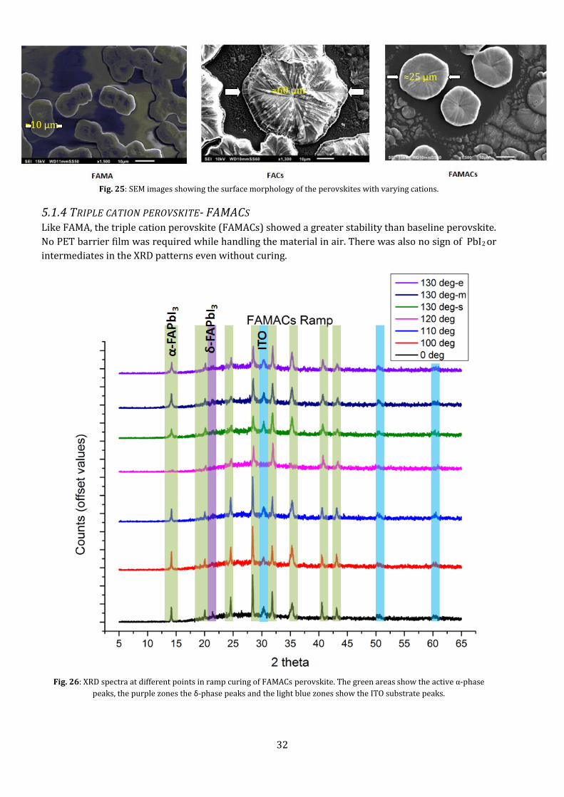
Fig. 25: SEM images showing the surface morphology of the perovskites with varying cations.
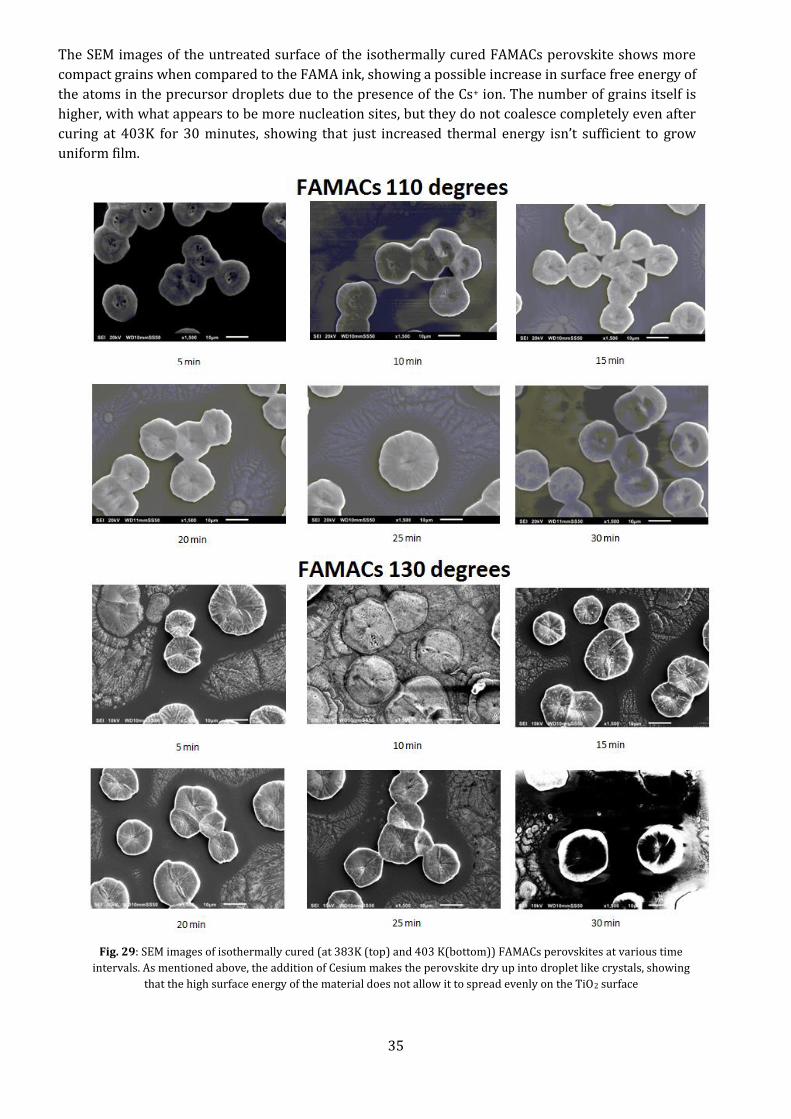
5.1.4 TRIPLE CATION PEROVSKITE- FAMACS Like FAMA, the triple cation perovskite (FAMACs) showed a greater stability than baseline perovskite.
No PET barrier film was required while handling the material in air. There was also no sign of PbI2 or
intermediates in the XRD patterns even without curing.
Fig. 26: XRD spectra at different points in ramp curing of FAMACs perovskite. The green areas show the active α-phase
peaks, the purple zones the δ-phase peaks and the light blue zones show the ITO substrate peaks.
≈10 μm
≈60 μm
≈25 μm

33
From Fig. 26, we can see that unlike FAMA, FAMACs perovskite shows reduced tendency to form δ-
phase. As discussed earlier, this is due to the stabilising influence of the Cs ion. With the added effect
of the MA+ ion, a more complete conversion of the precursor into the perovskite phase is possible.
Fig. 27: XRD peaks of FAMACs perovskite formed at various temperatures during ramp curing.
Again, the (002) facet appears to be the predominant orientation, with a calculated lattice parameter
of ≈0.6247 nm. As the cure time increases, the peaks shift right, towards higher 2θ angles. This is
accompanied by an overall decrease in the calculated lattice size, from 0.6277 nm at start of ramp
curing to 0.6247 nm at the end.
To see the effect of duration of curing, we look at the peaks under isothermal curing. At 403 K, all of
the δ-phase disappears even at 5 minutes of curing. But as the cure time increases, degradation
occurs, causing the perovskite to break down into PbI2 after 20 minutes of curing. Thus, 15 minutes of
curing at 403 K was fixed as optimum curing step.

34
Fig. 28: (Above) the XRD patterns from isothermal curing of FAMACs perovskite, showing the shifts caused by different
curing times.
35
The SEM images of the untreated surface of the isothermally cured FAMACs perovskite shows more
compact grains when compared to the FAMA ink, showing a possible increase in surface free energy of
the atoms in the precursor droplets due to the presence of the Cs+ ion. The number of grains itself is
higher, with what appears to be more nucleation sites, but they do not coalesce completely even after
curing at 403K for 30 minutes, showing that just increased thermal energy isn’t sufficient to grow
uniform film.
Fig. 29: SEM images of isothermally cured (at 383K (top) and 403 K(bottom)) FAMACs perovskites at various time
intervals. As mentioned above, the addition of Cesium makes the perovskite dry up into droplet like crystals, showing
that the high surface energy of the material does not allow it to spread evenly on the TiO2 surface
36
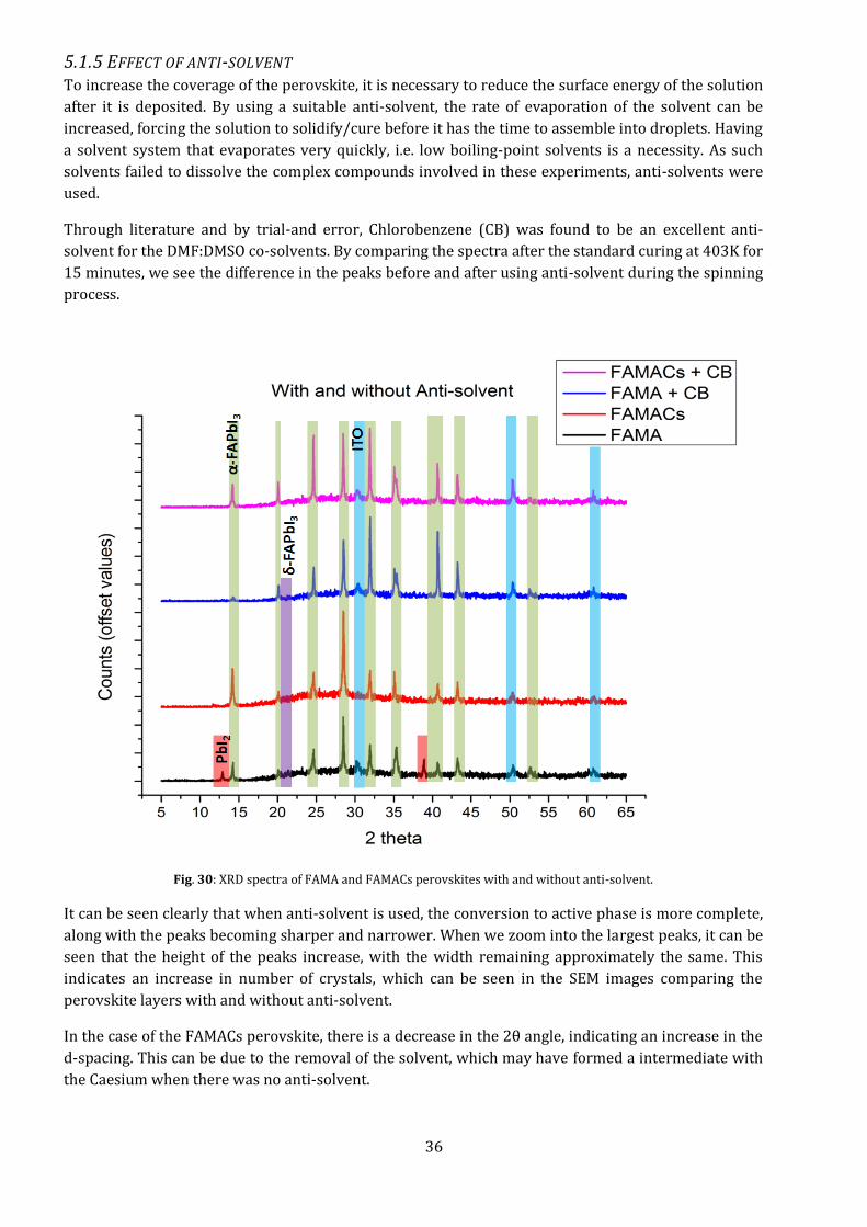
5.1.5 EFFECT OF ANTI-SOLVENT To increase the coverage of the perovskite, it is necessary to reduce the surface energy of the solution
after it is deposited. By using a suitable anti-solvent, the rate of evaporation of the solvent can be
increased, forcing the solution to solidify/cure before it has the time to assemble into droplets. Having
a solvent system that evaporates very quickly, i.e. low boiling-point solvents is a necessity. As such
solvents failed to dissolve the complex compounds involved in these experiments, anti-solvents were
used.
Through literature and by trial-and error, Chlorobenzene (CB) was found to be an excellent anti-
solvent for the DMF:DMSO co-solvents. By comparing the spectra after the standard curing at 403K for
15 minutes, we see the difference in the peaks before and after using anti-solvent during the spinning
process.
Fig. 30: XRD spectra of FAMA and FAMACs perovskites with and without anti-solvent.
It can be seen clearly that when anti-solvent is used, the conversion to active phase is more complete,
along with the peaks becoming sharper and narrower. When we zoom into the largest peaks, it can be
seen that the height of the peaks increase, with the width remaining approximately the same. This
indicates an increase in number of crystals, which can be seen in the SEM images comparing the
perovskite layers with and without anti-solvent.
In the case of the FAMACs perovskite, there is a decrease in the 2θ angle, indicating an increase in the
d-spacing. This can be due to the removal of the solvent, which may have formed a intermediate with
the Caesium when there was no anti-solvent.
37
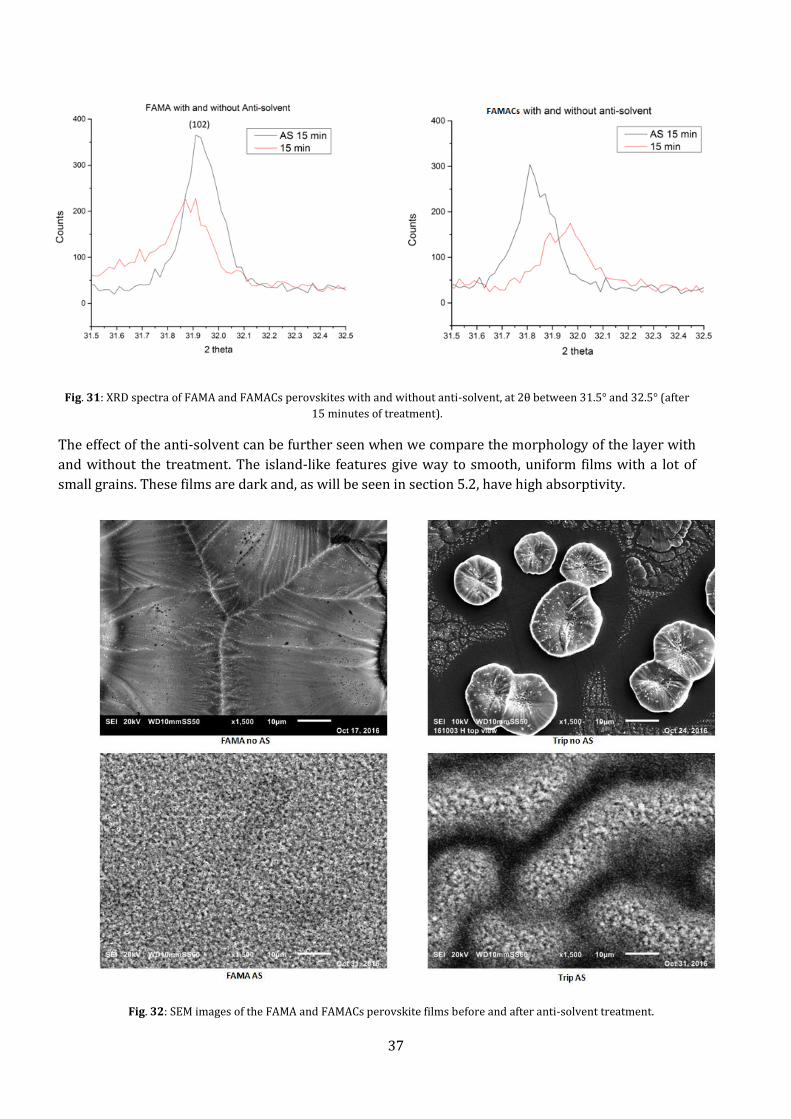
Fig. 31: XRD spectra of FAMA and FAMACs perovskites with and without anti-solvent, at 2θ between 31.5° and 32.5° (after
15 minutes of treatment).
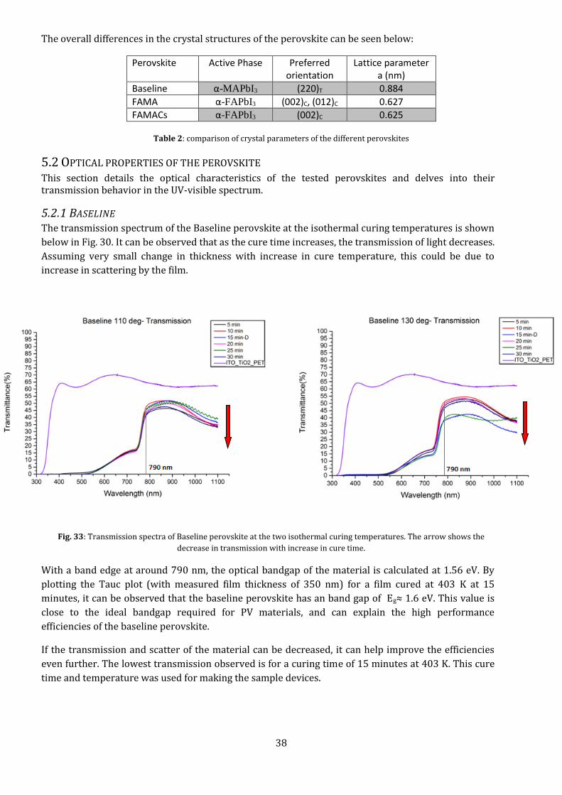
The effect of the anti-solvent can be further seen when we compare the morphology of the layer with
and without the treatment. The island-like features give way to smooth, uniform films with a lot of
small grains. These films are dark and, as will be seen in section 5.2, have high absorptivity.
Fig. 32: SEM images of the FAMA and FAMACs perovskite films before and after anti-solvent treatment.
38
The overall differences in the crystal structures of the perovskite can be seen below:
Perovskite Active Phase Preferred orientation
Lattice parameter a (nm)
Baseline α-MAPbI3 (220)T 0.884
FAMA α-FAPbI3 (002)C, (012)C 0.627
FAMACs α-FAPbI3 (002)C 0.625
Table 2: comparison of crystal parameters of the different perovskites
5.2 OPTICAL PROPERTIES OF THE PEROVSKITE This section details the optical characteristics of the tested perovskites and delves into their transmission behavior in the UV-visible spectrum.
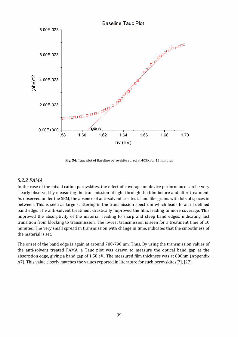
5.2.1 BASELINE The transmission spectrum of the Baseline perovskite at the isothermal curing temperatures is shown
below in Fig. 30. It can be observed that as the cure time increases, the transmission of light decreases.
Assuming very small change in thickness with increase in cure temperature, this could be due to
increase in scattering by the film.
Fig. 33: Transmission spectra of Baseline perovskite at the two isothermal curing temperatures. The arrow shows the
decrease in transmission with increase in cure time.
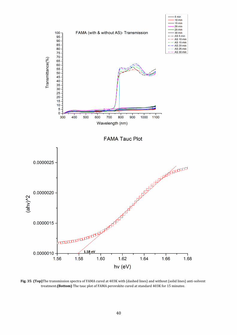
With a band edge at around 790 nm, the optical bandgap of the material is calculated at 1.56 eV. By
plotting the Tauc plot (with measured film thickness of 350 nm) for a film cured at 403 K at 15
minutes, it can be observed that the baseline perovskite has an band gap of Eg≈ 1.6 eV. This value is
close to the ideal bandgap required for PV materials, and can explain the high performance
efficiencies of the baseline perovskite.
If the transmission and scatter of the material can be decreased, it can help improve the efficiencies
even further. The lowest transmission observed is for a curing time of 15 minutes at 403 K. This cure
time and temperature was used for making the sample devices.
39
Fig. 34: Tauc plot of Baseline perovskite cured at 403K for 15 minutes
5.2.2 FAMA In the case of the mixed cation perovskites, the effect of coverage on device performance can be very
clearly observed by measuring the transmission of light through the film before and after treatment.
As observed under the SEM, the absence of anti-solvent creates island like grains with lots of spaces in
between. This is seen as large scattering in the transmission spectrum which leads to an ill defined
band edge. The anti-solvent treatment drastically improved the film, leading to more coverage. This
improved the absorptivity of the material, leading to sharp and steep band edges, indicating fast
transition from blocking to transmission. The lowest transmission is seen for a treatment time of 10
minutes. The very small spread in transmission with change in time, indicates that the smoothness of
the material is set.
The onset of the band edge is again at around 780-790 nm. Thus, By using the transmission values of
the anti-solvent treated FAMA, a Tauc plot was drawn to measure the optical band gap at the
absorption edge, giving a band gap of 1.58 eV.. The measured film thickness was at 800nm (Appendix
A7). This value closely matches the values reported in literature for such perovskites[7], [27].
40
Fig. 35: (Top)The transmission spectra of FAMA cured at 403K with (dashed lines) and without (solid lines) anti-solvent
treatment.(Bottom) The tauc plot of FAMA perovskite cured at standard 403K for 15 minutee.
41
In order to use this perovskite precursor without the additional anti-solvent step (fewer steps better
for scale up), additives need to be found to help increase the coverage of the material and improve
absorption.
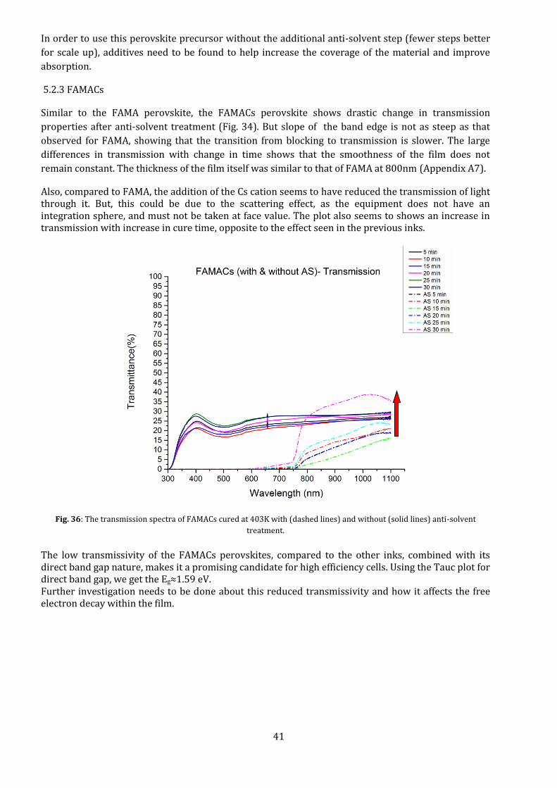
5.2.3 FAMACs
Similar to the FAMA perovskite, the FAMACs perovskite shows drastic change in transmission
properties after anti-solvent treatment (Fig. 34). But slope of the band edge is not as steep as that
observed for FAMA, showing that the transition from blocking to transmission is slower. The large
differences in transmission with change in time shows that the smoothness of the film does not
remain constant. The thickness of the film itself was similar to that of FAMA at 800nm (Appendix A7).
Also, compared to FAMA, the addition of the Cs cation seems to have reduced the transmission of light through it. But, this could be due to the scattering effect, as the equipment does not have an integration sphere, and must not be taken at face value. The plot also seems to shows an increase in transmission with increase in cure time, opposite to the effect seen in the previous inks.
Fig. 36: The transmission spectra of FAMACs cured at 403K with (dashed lines) and without (solid lines) anti-solvent
treatment.
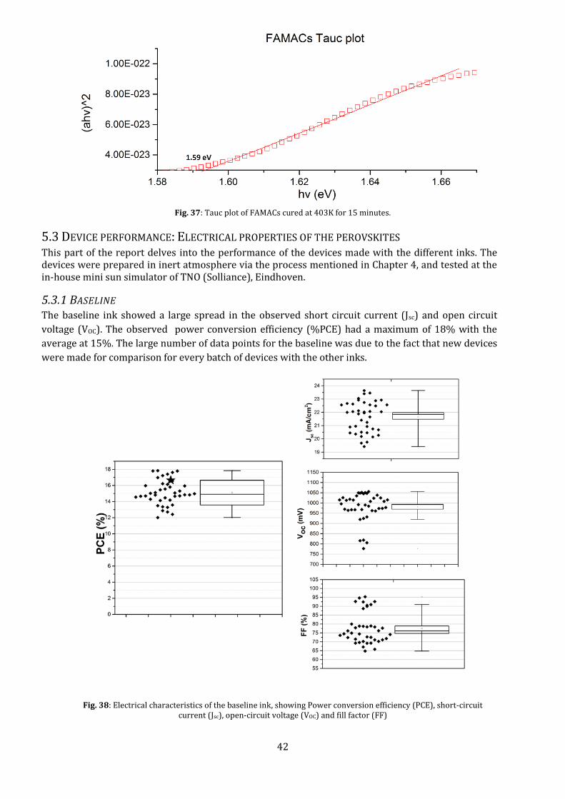
The low transmissivity of the FAMACs perovskites, compared to the other inks, combined with its direct band gap nature, makes it a promising candidate for high efficiency cells. Using the Tauc plot for direct band gap, we get the Eg≈1.59 eV. Further investigation needs to be done about this reduced transmissivity and how it affects the free electron decay within the film.
42
Fig. 37: Tauc plot of FAMACs cured at 403K for 15 minutes.
5.3 DEVICE PERFORMANCE: ELECTRICAL PROPERTIES OF THE PEROVSKITES This part of the report delves into the performance of the devices made with the different inks. The devices were prepared in inert atmosphere via the process mentioned in Chapter 4, and tested at the in-house mini sun simulator of TNO (Solliance), Eindhoven.
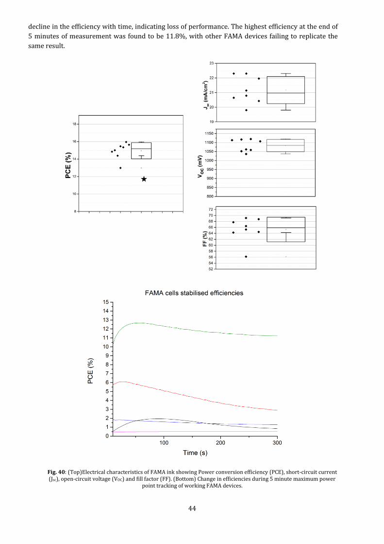
5.3.1 BASELINE The baseline ink showed a large spread in the observed short circuit current (Jsc) and open circuit
voltage (VOC). The observed power conversion efficiency (%PCE) had a maximum of 18% with the
average at 15%. The large number of data points for the baseline was due to the fact that new devices
were made for comparison for every batch of devices with the other inks.
Fig. 38: Electrical characteristics of the baseline ink, showing Power conversion efficiency (PCE), short-circuit
current (Jsc), open-circuit voltage (VOC) and fill factor (FF)

43
The low average VOC of 1000 mV was offset by the high average current (JSC) of ≈22 mA.cm-2 and fill
factor (FF)of 75%. The change in the maximum power point (MPP) of the devices were measured over
a period of 5 minutes (Fig. 39), and the observed efficiency showed very small change. The maximum
observed stabilised efficiency is represented as a star in Fig. 38.
Fig. 39: Change in efficiencies during 5 minute maximum power point tracking of working baseline devices.
This stability though depended on keeping the devices in an inert atmosphere during measurements.
The tendency of the baseline ink to degrade under humid conditions proved to be challenging when
handling or transporting the devices, before it was covered with a layer of the hole transport material
(HTM).
5.3.2 FAMA The FAMA ink showed a lower JSC and fill factors when compared to the baseline, but tended to have
similar efficiencies. With an average efficiency of ≈15% and a high VOC of nearly 1100 mV the FAMA
perovskite matches up to the Baseline in terms of performance. In addition, the films were stable
under humid conditions and did not degrade into photo-inactive tetragonal phase of FAPbI3 even after
a few days.
But it was not as reproducible, nor did it show a flat stabilised efficiency curve with time. The
reproducibility depended on factors such as mixing temperature, time between solution preparation
and device production and the purity of the lead source. The devices performed better when the
solution was stirred at room temperature overnight (12-15 hrs) and used coating the substrate after.
A higher purity halide source (TCI, 99.99%) gave a better performing ink (Appendix A4). This was
also observed in the case of the FAMACs perovskite. The following data is from devices made with the
TCI source PbI2.
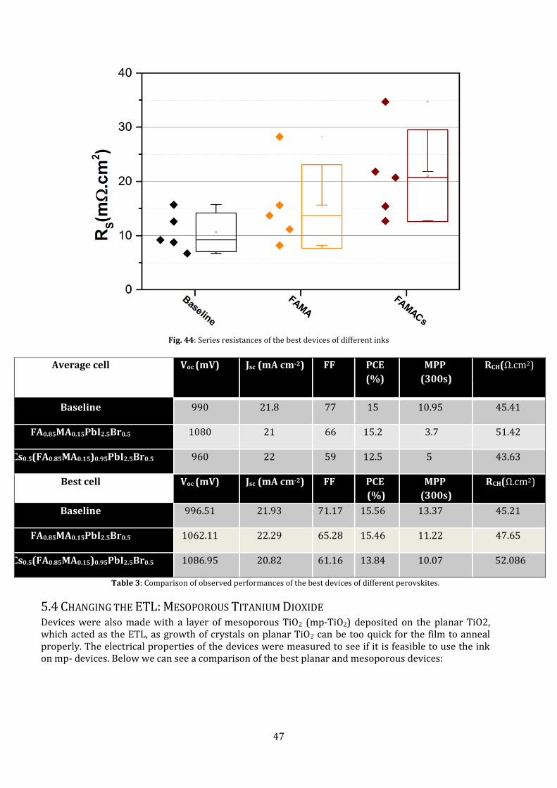
This difficulty in reproducing high performance devices is seen in the 5 minute efficiency
measurements during the maximum power point tracking of the devices. The curves show a slow
44
decline in the efficiency with time, indicating loss of performance. The highest efficiency at the end of
5 minutes of measurement was found to be 11.8%, with other FAMA devices failing to replicate the
same result.
Fig. 40: (Top)Electrical characteristics of FAMA ink showing Power conversion efficiency (PCE), short-circuit current (Jsc), open-circuit voltage (VOC) and fill factor (FF). (Bottom) Change in efficiencies during 5 minute maximum power
point tracking of working FAMA devices.

45
5.3.3 FAMACS PEROVSKITE FAMACs perovskites showed an increase in the short circuit currents, but a low fill factor meant the
device efficiency fell when compared to the previous two inks. These were the quickest films to
convert to the desired black phase, becoming dark immediately after coating. They were also the most
stable of the inks, withstanding exposure to humidity even before coating it with the protective HTL.
The inks showed improved stability, reproducing their performance even after 10 days (albeit while
stored under inert conditions). In Fig. 41, we see a comparison of the electrical performances of all the
FAMACs devices made.
Fig. 41: Electrical characteristics of FAMACs ink showing Power conversion efficiency (PCE), short-circuit current (Jsc), open-
circuit voltage (VOC) and fill factor (FF)
Under Maximum power point scans, the devices showed more stable efficiency curves when
compared to the FAMA devices with the highest efficiency of ≈10% after 5 minutes.

46
Fig. 42: Change in efficiencies during 5 minute maximum power point tracking of working FAMACs devices.
5.3.4 COMPARISON OF THREE INKS By taking the best performing devices of the three inks, we can also plot the current-voltage
characteristic curves for a comparison with the average values. From these, we can calculate the
characteristic and series resistances of the best devices and the average device.
Fig. 43: Current-Voltage characteristic curves of the best devices of different inks
The high resistances of the FAMACs inks showed that there is a possibility of increasing the current
density of the devices. The fact that the currents are comparable to the baseline devices even with
thigh resistances is encouraging. Table 3 also shows that the performance of the FAMA devices are
more comparable to baseline than FAMACs devices.
47
Fig. 44: Series resistances of the best devices of different inks
Average cell Voc (mV) Jsc (mA cm-2) FF PCE
(%)
MPP
(300s)
RCH(Ω.cm2)
Baseline 990 21.8 77 15 10.95 45.41
FA0.85MA0.15PbI2.5Br0.5 1080 21 66 15.2 3.7 51.42
Cs0.5(FA0.85MA0.15)0.95PbI2.5Br0.5 960 22 59 12.5 5 43.63
Best cell Voc (mV) Jsc (mA cm-2) FF PCE
(%)
MPP
(300s)
RCH(Ω.cm2)
Baseline 996.51 21.93 71.17 15.56 13.37 45.21
FA0.85MA0.15PbI2.5Br0.5 1062.11 22.29 65.28 15.46 11.22 47.65
Cs0.5(FA0.85MA0.15)0.95PbI2.5Br0.5 1086.95 20.82 61.16 13.84 10.07 52.086
Table 3: Comparison of observed performances of the best devices of different perovskites.
5.4 CHANGING THE ETL: MESOPOROUS TITANIUM DIOXIDE Devices were also made with a layer of mesoporous TiO2 (mp-TiO2) deposited on the planar TiO2, which acted as the ETL, as growth of crystals on planar TiO2 can be too quick for the film to anneal properly. The electrical properties of the devices were measured to see if it is feasible to use the ink on mp- devices. Below we can see a comparison of the best planar and mesoporous devices:
48
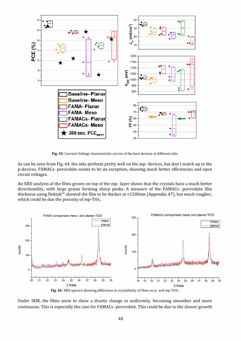
Fig. 45: Current-Voltage characteristic curves of the best devices of different inks
As can be seen from Fig. 44, the inks perform pretty well on the mp- devices, but don’t match up to the p-devices. FAMACs- perovskite seems to be an exception, showing much better efficiencies and open circuit voltages.
An XRD analysis of the films grown on top of the mp- layer shows that the crystals have a much better directionality, with large grains forming sharp peaks. A measure of the FAMACs- perovskite film thickness using Dektak™ showed the film to be thicker at ≈1200nm (Appendix A7), but much rougher, which could be due the porosity of mp-TiO2.
Fig. 46: XRD spectra showing difference in crystallinity of films on p- and mp-TiO2.
Under SEM, the films seem to show a drastic change in uniformity, becoming smoother and more
continuous. This is especially the case for FAMACs- perovskite. This could be due to the slower growth
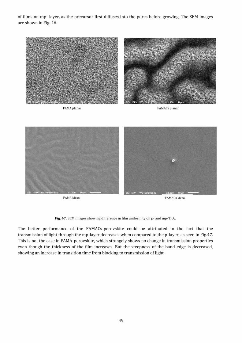
49
of films on mp- layer, as the precursor first diffuses into the pores before growing. The SEM images
are shown in Fig. 46.
Fig. 47: SEM images showing difference in film uniformity on p- and mp-TiO2.
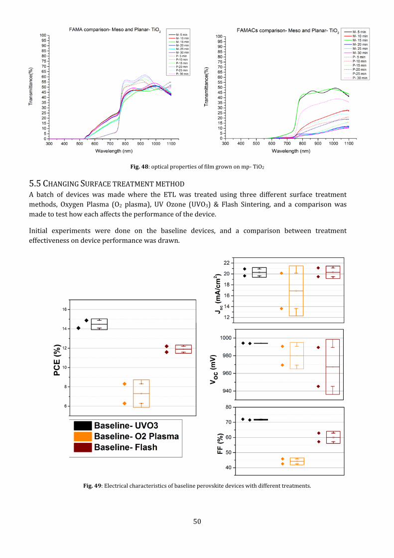
The better performance of the FAMACs-perovskite could be attributed to the fact that the
transmission of light through the mp-layer decreases when compared to the p-layer, as seen in Fig.47.
This is not the case in FAMA-perovskite, which strangely shows no change in transmission properties
even though the thickness of the film increases. But the steepness of the band edge is decreased,
showing an increase in transition time from blocking to transmission of light.
FAMA planar
FAMA Meso
FAMACs planar
FAMACs Meso
50
Fig. 48: optical properties of film grown on mp- TiO2
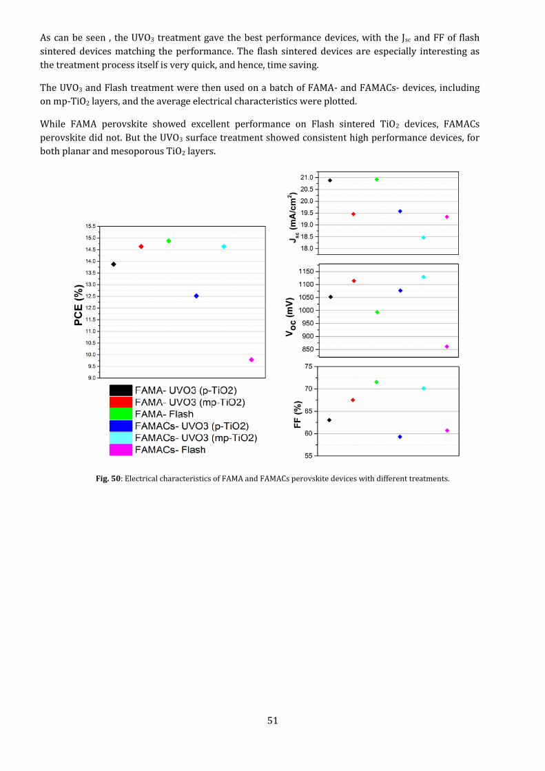
5.5 CHANGING SURFACE TREATMENT METHOD A batch of devices was made where the ETL was treated using three different surface treatment
methods, Oxygen Plasma (O2 plasma), UV Ozone (UVO3) & Flash Sintering, and a comparison was
made to test how each affects the performance of the device.
Initial experiments were done on the baseline devices, and a comparison between treatment
effectiveness on device performance was drawn.
Fig. 49: Electrical characteristics of baseline perovskite devices with different treatments.
51
As can be seen , the UVO3 treatment gave the best performance devices, with the Jsc and FF of flash
sintered devices matching the performance. The flash sintered devices are especially interesting as
the treatment process itself is very quick, and hence, time saving.
The UVO3 and Flash treatment were then used on a batch of FAMA- and FAMACs- devices, including
on mp-TiO2 layers, and the average electrical characteristics were plotted.
While FAMA perovskite showed excellent performance on Flash sintered TiO2 devices, FAMACs
perovskite did not. But the UVO3 surface treatment showed consistent high performance devices, for
both planar and mesoporous TiO2 layers.
Fig. 50: Electrical characteristics of FAMA and FAMACs perovskite devices with different treatments.
52
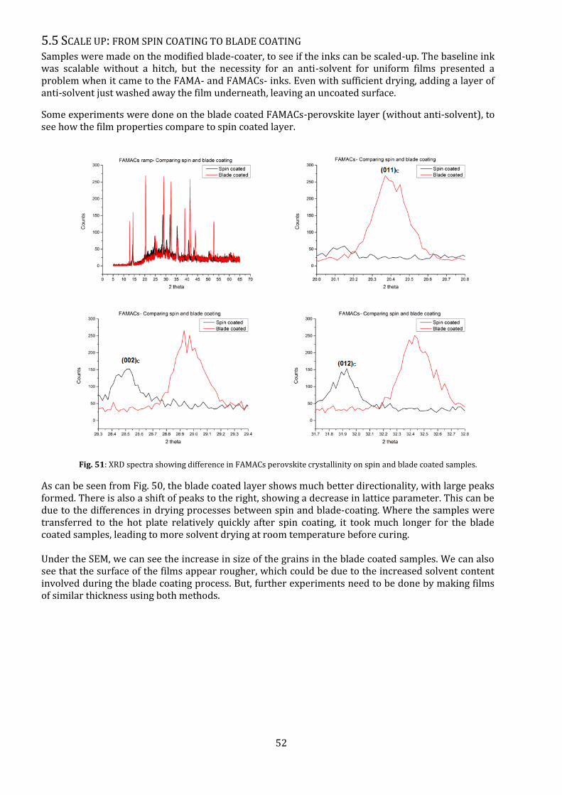
5.5 SCALE UP: FROM SPIN COATING TO BLADE COATING Samples were made on the modified blade-coater, to see if the inks can be scaled-up. The baseline ink was scalable without a hitch, but the necessity for an anti-solvent for uniform films presented a problem when it came to the FAMA- and FAMACs- inks. Even with sufficient drying, adding a layer of anti-solvent just washed away the film underneath, leaving an uncoated surface.
Some experiments were done on the blade coated FAMACs-perovskite layer (without anti-solvent), to see how the film properties compare to spin coated layer.
Fig. 51: XRD spectra showing difference in FAMACs perovskite crystallinity on spin and blade coated samples.
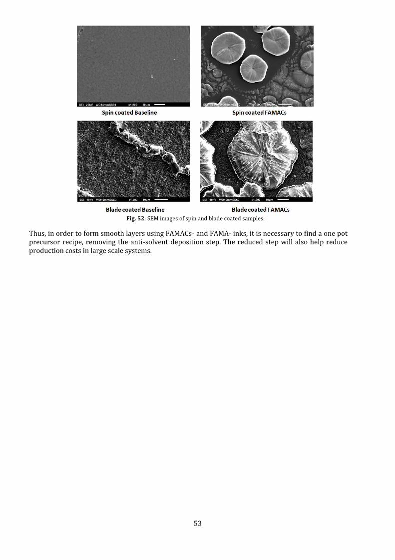
As can be seen from Fig. 50, the blade coated layer shows much better directionality, with large peaks formed. There is also a shift of peaks to the right, showing a decrease in lattice parameter. This can be due to the differences in drying processes between spin and blade-coating. Where the samples were transferred to the hot plate relatively quickly after spin coating, it took much longer for the blade coated samples, leading to more solvent drying at room temperature before curing. Under the SEM, we can see the increase in size of the grains in the blade coated samples. We can also see that the surface of the films appear rougher, which could be due to the increased solvent content involved during the blade coating process. But, further experiments need to be done by making films of similar thickness using both methods.
53
Fig. 52: SEM images of spin and blade coated samples.
Thus, in order to form smooth layers using FAMACs- and FAMA- inks, it is necessary to find a one pot precursor recipe, removing the anti-solvent deposition step. The reduced step will also help reduce production costs in large scale systems.

54
6. CONCLUSIONS AND RECOMMENDATIONS The aim of this project was to develop and characterize inks based on new cation mixtures to be used
for high efficiency perovskite devices. Though scale up of the chosen inks proved to be tough due to
the necessity of anti-solvent treatment, other useful conclusions could be drawn.
The mixed cation perovskites (FA0.85MA0.15PbI2.5Br0.5 (FAMA) and
Cs0.05(FA0.85MA0.15)0.95PbI2.5Br0.5 (FAMACs)) showed an increased stability under humid
conditions, remaining in their active phases and not degrading. This improved stability could
be due to the cations stabilising the active phase during curing. But the presence of such
varied ions along with the halides proved to be difficult to dissolve without using co-solvents.
The mixed cation mixture followed the Volmer-Weber film growth mode, where the deposited
precursor formed into island-like structures upon curing. This necessitated the anti-solvent, as
even increasing the thermal energy did not lead to the islands coalescing to form a uniform
film. Further experiments need to be done to find additives that can be mixed with the
precursors that can be used to bring down the surface energy and make a uniform perovskite
layer in a single deposition step.
The purity of the iodide source was important for device performance, with a 99.99% trace
metal basis PbI2 solution performing better. Higher purity lead source should be used for
future experiments.
While the FAMA ion mixture showed large scattering and incomplete conversion of lead iodide
at cure temperatures below 383K, the performance of the devices made with the ink matched
that of the baseline devices, with average Power conversion efficiency (PCE) of 15.2% and
average open circuit voltages VOC≈1100 mV. Combined with its stability under humid
conditions, this ink is suitable for further experiments.
The Cs+ ion increased the size of the grains and greatly improved the stability of the perovskite
layer, while also showing a capability for making high efficiency devices (with an average
power conversion efficiency of 12.5%) with excellent current generation (avg. JSC of 22
mA/cm-2) . But it’s somewhat lowered voltage (avg. VOC≈960mV), high series resistance (21
mΩ.cm2) and fill factor (avg. 59) indicated further work needs to be done to improve it.
Additives and doping with active ions like Li+, which have excellent charge transport
properties, may help with their improvement.
Both the mixed cation inks showed bandgaps closed to the ideal 1.5eV required for PV devices,
and improvement in film coverage by improving the solvent drying rate may help in tuning
their bandgap for different devices.
The mixed cation inks can be grown on both planar and mesoporous ETL, allowing greater
flexibility in the device design. While the addition of the mesoporous layer may be an extra
step for Roll-to-Roll (R2R) production, it should be noted that for FAMACs inks, mp-TiO2
devices showed better voltage and fill factor characteristics than the planar devices.

55
All three inks show good performance on UV-ozone treated TiO2 layer, which can be used as
the basic surface treatment for future device production. Flash-sintering shows promise as an
ultra-fast surface treatment alternative, and further experiments need to be done in adapting
it for scaled up production (R2R).

56
7. REFERENCES [1] A. Kojima, K. Teshima, Y. Shirai, and T. Miyasaka, “Organometal halide perovskites
as visible-light sensitizers for photovoltaic cells,” J. Am. Chem. Soc., vol. 131, no. 17,
pp. 6050–6051, May 2009.
[2] M. a. Green, a. Ho-Baillie, and H. J. Snaith, “The emergence of perovskite solar
cells,” Nat. Photonics, vol. 8, no. 7, pp. 506–514, 2014.
[3] N. J. Jeon et al., “Compositional engineering of perovskite materials for high-
performance solar cells,” Nature, vol. 517, no. 7535, pp. 476–480, 2015.
[4] M. Saliba et al., “Cesium-containing Triple Cation Perovskite Solar Cells: Improved
Stability, Reproducibility and High Efficiency,” Energy Environ. Sci., vol. 9, no. 6,
pp. 1989–1997, 2016.
[5] J. Gong, S. B. Darling, and F. You, “Perovskite photovoltaics: life-cycle assessment
of energy and environmental impacts,” Energy Environ. Sci., vol. 8, no. 7, pp. 1953–
1968, 2015.
[6] “efficiency_chart.jpg (4349×2456).” [Online]. Available:
http://www.nrel.gov/pv/assets/images/efficiency_chart.jpg.
[7] G. E. Eperon, S. D. Stranks, C. Menelaou, M. B. Johnston, L. M. Herz, and H. J. Snaith,
“Supplementary information Formamidinium of Formamidinium lead trihalide: a
broadly tunable perovskite for efficient planar heterojunction solar cells,” Energy
Environ. Sci., vol. 7, no. 3, p. 982, 2014.
[8] A. Binek, F. C. Hanusch, P. Docampo, and T. Bein, “Stabilization of the trigonal
high-temperature phase of formamidinium lead iodide,” J. Phys. Chem. Lett., vol. 6,
no. 7, pp. 1249–1253, 2015.
[9] W. Zhang et al., “Ultrasmooth organic-inorganic perovskite thin-film formation
and crystallization for efficient planar heterojunction solar cells,” Nat Commun,
vol. 6, p. 6142, 2015.
[10] J. T. Jacobsson et al., “An exploration of the compositional space for mixed lead
halogen perovskites for high efficiency devices - SI,” Energy Environ. Sci., vol. 41,
no. 0, pp. 1–35, 2016.
[11] C. Quarti et al., “Structural and optical properties of methylammonium lead iodide
across the tetragonal to cubic phase transition: implications for perovskite solar
cells,” Energy Environ. Sci., vol. 9, pp. 155–163, 2016.
[12] S. Razza et al., “Perovskite solar cells and large area modules (100 cm2) based on
an air flow-assisted PbI2 blade coating deposition process,” J. Power Sources, vol.
277, pp. 286–291, 2015.
[13] K. Hwang et al., “Toward Large Scale Roll-to-Roll Production of Fully Printed
Perovskite Solar Cells,” Adv. Mater., vol. 27, no. 7, pp. 1241–1247, Feb. 2015.
[14] S. T. Williams, A. Rajagopal, C. C. Chueh, and A. K. Y. Jen, “Current Challenges and
Prospective Research for Upscaling Hybrid Perovskite Photovoltaics,” J. Phys.
Chem. Lett., vol. 7, no. 5, pp. 811–819, 2016.
[15] G. E. Eperon, V. M. Burlakov, P. Docampo, A. Goriely, and H. J. Snaith,
“Morphological control for high performance, solution-processed planar
heterojunction perovskite solar cells,” Adv. Funct. Mater., vol. 24, no. 1, pp. 151–
157, 2014.

57
[16] N. J. Jeon, J. H. Noh, Y. C. Kim, W. S. Yang, S. Ryu, and S. Il Seok, “Solvent
engineering for high-performance inorganic-organic hybrid perovskite solar
cells.,” Nat. Mater., vol. 13, no. July, pp. 1–7, 2014.
[17] D. P. McMeekin et al., “A mixed-cation lead mixed-halide perovskite absorber for
tandem solar cells,” Science (80-. )., vol. 351, no. 6269, pp. 151–155, 2016.
[18] A. N. Interdisciplinary and M. I. T. Study, “The Future of Solar Energy.”
[19] “BandDiagramSolarCell-en.png (816×684).” [Online]. Available:
https://upload.wikimedia.org/wikipedia/commons/7/77/BandDiagramSolarCell
-en.png.
[20] W. Shockley and H. J. Queisser, “Detailed balance limit of efficiency of p-n junction
solar cells,” J. Appl. Phys., vol. 32, no. 3, pp. 510–519, 1961.
[21] Z. Cheng and J. Lin, “Layered organic–inorganic hybrid perovskites: structure,
optical properties, film preparation, patterning and templating engineering,”
CrystEngComm, vol. 12, pp. 2646–2662, 2010.
[22] C. Li, X. Lu, W. Ding, L. Feng, Y. Gao, and Z. Guo, “Formability of ABX 3 (X = F, Cl, Br,
I) halide perovskites,” Acta Crystallogr. Sect. B Struct. Sci., vol. 64, no. 6, pp. 702–
707, 2008.
[23] G. Nedelcu, L. Protesescu, S. Yakunin, M. I. Bodnarchuk, M. J. Grotevent, and M. V.
Kovalenko, “Fast Anion-Exchange in Highly Luminescent Nanocrystals of Cesium
Lead Halide Perovskites (CsPbX<inf>3</inf>, X = Cl, Br, I),” Nano Lett., vol. 15, no.
8, pp. 5635–5640, 2015.
[24] T. Baikie et al., “Synthesis and crystal chemistry of the hybrid perovskite
(CH3NH3)PbI3 for solid-state sensitised solar cell applications,” J. Mater. Chem. A,
vol. 1, no. 18, p. 5628, 2013.
[25] S. A. Bretschneider, J. Weickert, J. A. Dorman, and L. Schmidt-Mende, “Research
update: Physical and electrical characteristics of lead halide perovskites for solar
cell applications,” APL Mater., vol. 2, no. 4, 2014.
[26] A. Poglitsch and D. Weber, “Dynamic disorder in
methylammoniumtrihalogenoplumbates (II) observed by millimeter-wave
spectroscopy,” J. Chem. Phys., vol. 87, no. 11, p. 6373, 1987.
[27] A. Amat et al., “Cation-induced band-gap tuning in organohalide perovskites:
Interplay of spin-orbit coupling and octahedra tilting,” Nano Lett., vol. 14, no. 6,
pp. 3608–3616, 2014.
[28] N. Pellet et al., “Mixed-organic-cation perovskite photovoltaics for enhanced
solar-light harvesting,” Angew. Chemie - Int. Ed., vol. 53, no. 12, pp. 3151–3157,
2014.
[29] W. S. Yang et al., “High-performance photovoltaic perovskite layers fabricated
through intramolecular exchange,” Science (80-. )., vol. 348, no. May, p.
science.aaa9272-, 2015.
[30] T.-B. Song et al., “Perovskite solar cells: film formation and properties,” J. Mater.
Chem. A, vol. 3, no. 17, pp. 9032–9050, 2015.
[31] J. G. Tait et al., “Determination of Solvent Systems for Blade Coating Thin Film
Photovoltaics,” Adv. Funct. Mater., pp. 3393–3398, 2015.
[32] W. Huang, J. S. Manser, P. V. Kamat, and S. Ptasinska, “Evolution of Chemical
Composition, Morphology, and Photovoltaic Efficiency of CH3NH3PbI3 Perovskite

58
under Ambient Conditions,” Chem. Mater., vol. 28, no. 1, pp. 303–311, 2016.
[33] F. C. Hanusch et al., “Efficient planar heterojunction perovskite solar cells based
on formamidiniumlead bromide,” J. Phys. Chem. Lett., vol. 5, no. 16, pp. 2791–
2795, 2014.
[34] T. Zhang et al., “Profiling the Organic Cation-dependent Degradation of
Organolead Halide Perovskite Solar Cells,” J. Mater. Chem. A, vol. 5, pp. 1103–
1111, 2016.
[35] Z. Song, S. C. Watthage, A. B. Phillips, and M. J. Heben, “Pathways toward high-
performance perovskite solar cells: review of recent advances in organo-metal
halide perovskites for photovoltaic applications,” J. Photonics Energy, vol. 6, no. 2,
p. 22001, 2016.
[36] J. J. Choi, X. Yang, Z. M. Norman, S. J. L. Billinge, and J. S. Owen, “Structure of
Methylammonium Lead Iodide Within Mesoporous Titanium Dioxide : Active
Material in High Performance Perovskite Solar Cells Structure of
Methylammonium Lead Iodide Within Mesoporous Titanium Dioxide : Active
Material in High Performance Perovs,” 2013.
[37] H. Zhou et al., “Interface engineering of highly efficient perovskite solar cells,” vol.
345, no. 6196, pp. 542–546, 2014.
[38] J. You et al., “Improved air stability of perovskite solar cells via solution-processed
metal oxide transport layers,” Nat. Nanotechnol., vol. 11, no. 1, pp. 75–81, Oct.
2015.
[39] W. Chen et al., “Efficient and stable large-area perovskite solar cells with
inorganic charge extraction layers,” Science (80-. )., vol. 350, no. 6263, 2015.
[40] F. Di Giacomo et al., “Flexible perovskite photovoltaic modules and solar cells
based on atomic layer deposited compact layers and UV-irradiated
TiO<inf>2</inf> scaffolds on plastic substrates,” Adv. Energy Mater., vol. 5, no. 8,
2015.
[41] J. Troughton et al., “Photonic flash-annealing of lead halide perovskite solar cells
in 1 ms,” J. Mater. Chem. A, vol. 4, no. 9, pp. 3471–3476, 2016.
[42] P. W. Liang et al., “Additive enhanced crystallization of solution-processed
perovskite for highly efficient planar-heterojunction solar cells,” Adv. Mater., vol.
26, no. 22, pp. 3748–3754, 2014.
[43] D. T. Moore et al., “Crystallization kinetics of organic-inorganic trihalide
perovskites and the role of the lead anion in crystal growth,” J. Am. Chem. Soc., vol.
137, no. 6, pp. 2350–2358, 2015.
[44] K. Yan et al., “Hybrid Halide Perovskite Solar Cell Precursors: Colloidal Chemistry
and Coordination Engineering behind Device Processing for High Efficiency,” J.
Am. Chem. Soc., vol. 137, no. 13, pp. 4460–4468, 2015.
[45] W. Niu et al., “Applications of atomic layer deposition in solar cells.,”
Nanotechnology, vol. 26, no. 6, p. 64001, 2015.
[46] “Spin Coating: A Guide to Theory and Techniques – Ossila.” [Online]. Available:
https://www.ossila.com/pages/spin-coating.
[47] M. A. Green and M. A. Green, “Accurate expressions for solar cell fill factors
including series and shunt resistances Accurate expressions for solar cell fill
factors including series and shunt resistances,” vol. 81111, 2016.

59
[48] S. Luo and W. A. Daoud, “Crystal structure formation of CH3NH3Pbi3-xClx
perovskite,” Materials (Basel)., vol. 9, no. 3, pp. 1–13, 2016.
[49] A. A. Zhumekenov et al., “Formamidinium Lead Halide Perovskite Crystals with
Unprecedented Long Carrier Dynamics and Di ff usion Length,” 2016.
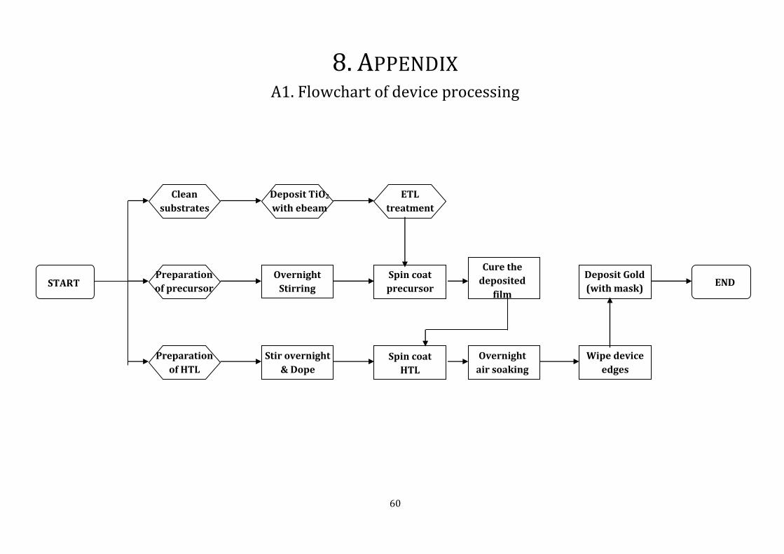
60
8. APPENDIX A1. Flowchart of device processing
START
Clean
substrates
Deposit TiO2
with ebeam
ETL
treatment
Preparation
of precursor
Overnight
Stirring
Spin coat
precursor
Preparation
of HTL
Stir overnight
& Dope
Cure the
deposited
film
Spin coat
HTL
Overnight
air soaking
Wipe device
edges
Deposit Gold
(with mask) END
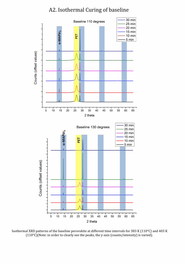
A2. Isothermal Curing of baseline
Isothermal XRD patterns of the baseline perovskite at different time intervals for 383 K (110°C) and 403 K
(110°C)(Note: in order to clearly see the peaks, the y-axis (counts/intensity) is varied).
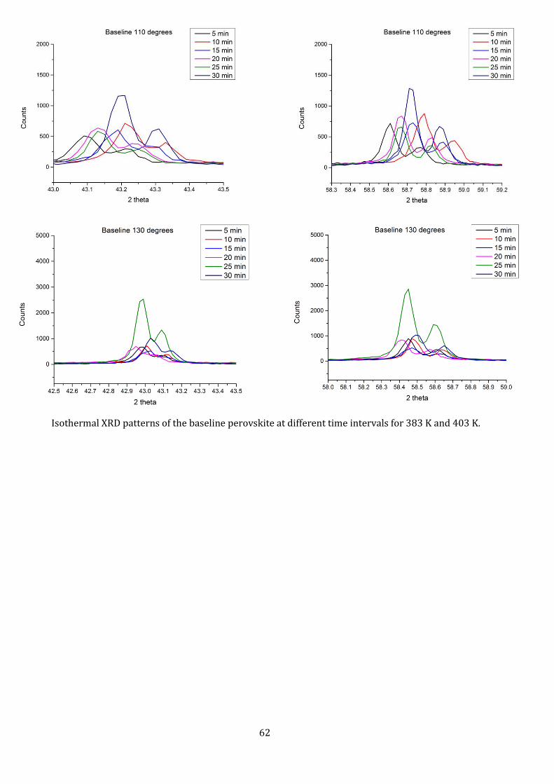
62
Isothermal XRD patterns of the baseline perovskite at different time intervals for 383 K and 403 K.

63
A3. Change in concentration of precursor solution

64
A4.Change in purity of lead source The SA stands for Sigma-Aldrich sourced PbI2 (99% purity trace metals basis) and TCI for the TCI sourced
PbI2 (99.99% purity trace metals basis).

65
A5. Relevant Pictures
(Top) FAMA (left) and FAMACs (left) cells 10 days after preparation. Note that the colour of the
film is still dark. (Bottom) Baseline cells after degradation.
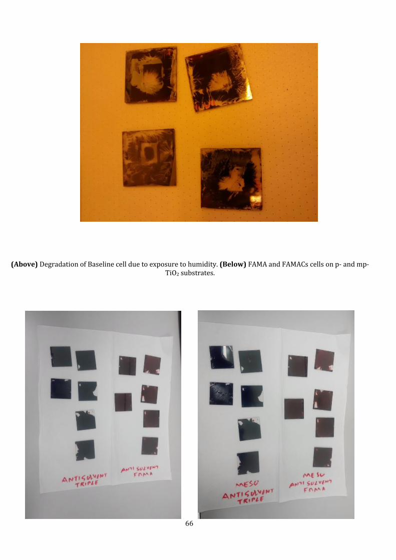
66
(Above) Degradation of Baseline cell due to exposure to humidity. (Below) FAMA and FAMACs cells on p- and mp- TiO2 substrates.
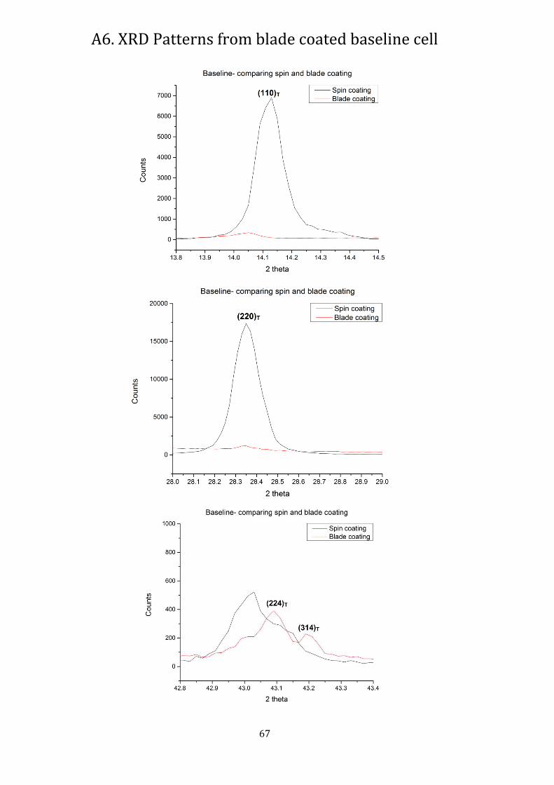
67
A6. XRD Patterns from blade coated baseline cell

68
A7. Thickness profile of the various films
FAMA and FAMACs films showing island-like morphology without (Top) and with (Bottom) anti-solvent
treatment.
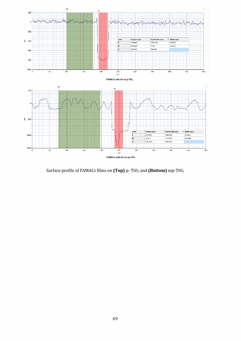
69
Surface profile of FAMACs films on (Top) p- TiO2 and (Bottom) mp-TiO2