device engineering of perovskite solar cells to achieve
TRANSCRIPT
1
Device Engineering of Perovskite Solar Cells to Achieve Near
Ideal Efficiency
Sumanshu Agarwal1 and Pradeep R. Nair2
1Department of Energy Science and Engineering, 2Department of Electrical Engineering
Indian Institute of Technology Bombay, Mumbai, Maharashtra, 400076, India

2
Abstract — Despite the exciting recent research on perovskite based solar cells, the design space
for further optimization and the practical limits of efficiency are not well known in the
community. In this manuscript, we address these aspects through theoretical calculations and
detailed numerical simulations. Here, we first provide the detailed balance limit efficiency in the
presence of radiative and Auger recombination. Then, using coupled optical and carrier transport
simulations, we identify the physical mechanisms that contribute towards bias dependent carrier
collection, and hence low fill factors of current perovskite based solar cells. Curiously, we find
that while Auger recombination is not a dominant factor at the detailed balance limit, it plays a
significant role in device level implementations. Surprisingly, our novel device designs indicate
that it is indeed possible to achieve efficiencies and fill factors greater than 25% and 85%,
respectively, with near ideal super-position characteristics even in the presence of Auger
recombination.
Keywords —detailed balance limit, fill factor, Auger recombination

3
I. INTRODUCTION
The recent reports on organic-inorganic perovskite based solar cells are indeed encouraging with
reported efficiencies of the order of 20%1,2 - a remarkable feat achieved within 3-4 years of
active research. Large diffusion length of carriers3–5 with large extinction coefficient6 makes
such perovskites an ideal material for solar cell application. While a comprehensive literature
survey is beyond the scope of this manuscript, we would like to mention that there has been
reports of high efficiency solar cells with combination of perovskite materials2, better
reproducibility7 and stability8, usage of flexible substrate9, organic materials as both electron
and hole transport layers10, large grain size perovskite fabrication11, perovskite based tandem
cell12,13, etc.. There has also been efforts towards better understanding of material properties14–16,
including the recombination strengths4,17–19 and mobility.4,19,20
Despite the above mentioned exciting achievements in experimental research on perovskite solar
cells, the corresponding theoretical understanding is lacking in many aspects. For example, while
the detailed balance limits of efficiency based on radiative recombination was already reported21,
the effect of Auger recombination is not clearly elucidated. Similarly, the performance limiting
factors of current solar cells are yet to be identified, and hence the path for further optimization is
ill defined. In this manuscript, we first identify the theoretical performance limits of perovskite
solar cells in the presence of radiative and Auger recombination (Section II). Then, through
detailed numerical simulations, we identify the physical mechanisms that contribute to sub-
optimal performance of current perovskite solar cells (see Fig. 1, also Section III). Finally, we
show that near ideal performance can be achieved through appropriate device designs, even in
the Auger recombination limit (Section IV).

4
II AUGER RECOMBINATION AND DETAILED BALANCE LIMITS
The theoretical performance limits of any single junction solar cell are well known in the
community since the landmark article by Shockley and Quiesser in 196122 and later updated by
Green23 and Tiedje et al.24 These performance limits are dictated by the fundamental
recombination mechanisms in the solar cell, as listed below
Fig. 1: Performance trends of recently reported perovskite solar cells1,2,26,33 (shown by
open circles). The shaded region shows the detailed balance limits (with only radiative
recombination) for and efficiency for a material with band gap in the range of 1.5-1.6
eV, while the red dot with error bar shows the detailed balance limit in the presence of
Auger recombination (assumed band gap of 1.55eV). Lower limit in error bar is
corresponding to Auger coefficient 1×10-28 cm6s-1 while upper limit correspond to Auger
coefficient 1×10-30 cm6s-1. The dotted curve and the solid circle indicate the possible
performance improvement in case of valid super-position between dark and light JV
characteristics of the data reported in ref.26

5
2
2 2
1 1
( )() ( )( ) ( )
i
i n p i
n p
Cnp n
R n A p np np
np np n n
A
(1)
In the above equation, denotes the recombination rate, the first term on the RHS denotes trap
assisted SRH recombination, the second term denotes the radiative recombination, and the third
term denotes the Auger recombination. Detailed balance limit calculations consider the radiative
and Auger recombination processes only. For perovskite solar cells, the detailed balance limit for
efficiency in the radiative limit is available in literature.21 However, the effect of Auger
recombination is not yet reported. Using the solar spectrum from NREL25, our calculations
indicate that for a material of band gap 1.55eV, the theoretical limit for the efficiency in the
presence of only radiative recombination (SQ limit) is 31.45% (with 27.3SCJ mA/cm2,
1.28OCV V, and the 90.3%FF ). While the SQ limits are the theoretical upper bounds for
efficiency, Auger recombination could influence the practical efficiency limits and are often
computed using the simplifying assumption of n p .23,24 Under such assumptions, the
corresponding performance parameters in the presence of Auger recombination are 27.3SCJ
mA/cm2, 1.17OCV V, 92.3%FF , and 29.48% (for a perovskite thickness of 300nm
using 291 10n pA AA cm6/s, which is very close to reported experimental results19).
Detailed theoretical calculations of these performance metrics are provided in section I of
Supplementary materials. We would like to mention that the above practical efficiency limit in
the presence of Auger recombination is very sensitive to the parameter in , the intrinsic carrier
concentration and the Auger recombination coefficient A . The intrinsic carrier concentration is
unknown for perovskites and we have used 6109in cm-3 in our calculations (i.e., based on an
assumption of 201 10C VN N cm-3 and 1.55gE eV, where CN and VN are the effective

6
density of states in the conduction and valence band, respectively). An order of magnitude
change in in , for
2911 0A cm6s-1, results in approximately 2% change in efficiency (see
section II of supplementary material for detail). Similarly, an order of change in A , for
6109in cm-3, leads to ~1% change in efficiency (see figure 1). Hence, accurate experimental
estimates of in and A is of paramount interest for the community.
III BIAS DEPENDENT CARRIER COLLECTION AND LOW FF
The achievable limits of efficiency for a solar cell could be much different from the theoretical
limits and is dictated by two aspects – (a) the dark JV characteristics darkJ and (b) the bias
dependent behavior of photo-generated carriers photoJ . These effects are succinctly captured by
the light JV characteristics, lightJ , given by
( ) ( ) ( )light photo darkJ V J V J V (2)
The above equation assumes that the dark current remains same during illuminated conditions as
well, which need not be universally valid. It is evident from eq. (2) that the optimal performance
for a given solar cell can be achieved only when the photo-current is bias independent. For such
cases, eq. (2) reduces to the well-known illuminated JV characteristics of a diode where the
principle of super-position is valid between the dark and light JV characteristics.
Figure 1 summarizes the efficiency vs. FF trade-off for some of the recently reported high
efficiency perovskite solar cells. We also illustrate the detailed balance limit efficiencies and the
theoretical FF limits in the same figure. Figure 1 indicates that while the current state of the art
perovskite solar cells lag significantly behind the theoretical limits of efficiency, the FF gap is

7
especially intriguing. Further, the physical mechanisms, that contribute toward this loss in
efficiency and FF , are not well known. More importantly, the practical efficiency limits, as
dictated by eq. (2), are also not clearly elucidated.
To further understand the practical limits of solar cell efficiency, we performed data analysis
using the experimental results reported by Liu et al.26 Figure 2a shows experimental dark and
light JV characteristics (open symbols). Also plotted is the expected JV characteristics based on
super-position principle (dashed curve). It is evident from Fig. 2a that the principle of
superposition does not hold for these reported devices and the photocurrent is indeed bias
dependent. Curiously, we find that if the photo-current were bias independent, the principle of
Fig. 2: Dark and light JV of the
perovskite solar cell as reported by Liu
et al.26 (open symbols). Solid lines are
the corresponding simulation results.
Dashed curve represents the dark JV
downshifted by , i.e. expected light
JV in case of valid superposition.
Simulated photon absorption profile
inside perovskite material is shown in
inset of part a. Part b represents the
energy band diagram of device under
equilibrium and at 0.9V in dark
(black) and light (blue).

8
super-position indicates that the upper limit of achievable efficiency for the same device is 20%
with a FF of 75%. This indicates that bias dependent carrier collection alone results in a loss in
efficiency of around 5% for these reported devices. Further, the FF from super-position is still
much lower than the detailed balance limits (see Fig. 1). This indicates that there is still enough
scope to improve the efficiency by better device design that could result in lower dark current
(see eq. (2)). Hence it is evident that the current efficiencies could be significantly improved if
the physical mechanisms that contribute towards dark current, bias dependent carrier collection
and recombination could be identified.
We performed detailed numerical simulations to explore the physical mechanisms that lead to
bias dependent carrier collection. Fig. 2a shows a comparison between experimental results
(open symbols) from literature26 and our simulation results (solid lines). The essential physical
mechanisms to consider in any solar cell are (a) the carrier generation rate due to optical
absorption and (b) the bias dependent carrier collection at appropriate electrodes in the presence
of various recombination mechanisms. To address (a), we used the transfer matrix methodology,
described by Pettersson et al.27, to estimate the optical absorption and hence the carrier
generation rate inside perovskite material. For a thickness of 300 nm for the perovskite layer, our
simulations indicate that (see inset of Fig. 2a) the net optical absorption in perovskite material
could correspond to a SCJ ~21.5 mA/cm2 (under the assumption that all photo-generated carriers
are collected at short circuit conditions28), which is very close to the experimental results
reported by Liu et al.26 With calibrated estimates for carrier generation rates, we addressed the
carrier collection through self-consistent solution of continuity and Poisson’s equations.29,30 We
neglect the role of excitons, whose effects were shown to be negligible at low illumination
intensities17 (i.e. 1 Sun). Our simulation methodology and parameters are calibrated with

9
experimental results, as reported previously31, and the details are provided in Section IV and V
of supplementary materials.
In self-consistent simulation of Poisson and carrier continuity equations, we explicitly considered
all the recombination mechanisms listed in eq. (1). Specifically, we assumed temperature
independent auger recombination (see eq. 1), with 291 10n pA A cm6s-1, a value very close
to that literature reports.19 The radiative recombination rate estimated theoretically using Van
Roosbroeck model32 ( 1312 0C cm3s-1, see section III of supplementary material) vary
significantly from the corresponding rates obtained from Photoluminiscence decay17,18 (
101~ 1 0C cm3s-1). Hence, we assumed 1113 0C cm3s-1 in our numerical simulations. The
experimentally observed dark current ideality factor is close to 2, which indicates significant trap
assisted recombination. This allows one to estimate the minority carrier lifetime (assuming
n p see eq. (1)) from the relation0
2 scoc
JkTV lnq J
, where0 ~
2inW
J
, W being the
thickness of perovskite layer (see ref.29). Using the experimental results for 1.07OCV V,
21.5SCJ mAcm-2, and 300W nm, the above relations indicate that is the order of 610 s for
perovskite. Note that this estimate is very close to that obtained from PL measurements.4
Through detailed simulations, we find that 62.73 10 s and 0.2 cm2/Vs (where is the
mobility of charge carrier in the perovskite) along with the before mentioned parameters for
radiative and Auger recombination can anticipate all the relevant features of experimental dark
and light IV. The assumed value for mobility along with the above mentioned minority carrier
lifetime gives a diffusion length of around 1μm, close to the reported experimental results.3

10
Interestingly, our simulations could reproduce all relevant features of dark
J , which includes a
diode ideality factor of 2 indicating trap assisted process as the dominant recombination
mechanism and a large bias voltage exponent of 2 which indicates the space charge limited
transport (corresponding parameters are extracted in section V of supplementary materials and
ref.31). In addition to this, a perfect agreement between numerical simulations and experimental
results is observed for the light JV characteristics for all relevant parameters likeSCJ , FF , and
OCV , thus validating the simulation methodology and the material parameters used. The energy
band diagrams shown in Fig. 2b provide important insights towards the bias dependence of
photocurrent. It is evident that the high band offsets at ETL/perovskite junction and
perovskite/HTL junction act as near ideal blocking contacts. Equilibrium band diagram shown
in fig. 2b suggest that till biV V (bi
V is the built in potential), the photogenerated carriers will
be collected effectively by the contact layers. When applied bias is more than biV , the electric
field in the perovskite and ETL/HTL layers is not favorable for carrier collection at desired
contacts. This bias dependent carrier collection in turn leads increased recombination of photo-
generated carriers in perovskite layer. As a result the photocurrent shows a bias dependence thus
limiting the efficiencies with low FF .
IV PRACTICAL EFFICIENCY LIMITS
The results shown in Fig. 2 indicate that the bias dependence of photocurrent is due to the fact
that the collection of photo-generated carriers is mainly transport limited. It is now evident that
to reduce the bias dependence of photocurrent, one should ensure that carrier transport through
the entire device is also bias independent – i.e., the electric field assisted drift component should
be reduced while increasing the diffusive carrier transport. The E-B diagram in Fig. 2 indicates

11
that significant bias dependent carrier transport occurs in both the perovskite as well as the
contact layers. Increasing the mobility of carriers in the contact layers is expected to improve the
FF , however, this might not be enough to reduce the bias dependence (see Section VI of
Supplementary materials for a detailed discussion on this). Curiously, the carrier collection can
be made effectively bias independent if the various layers are doped appropriately. We will now
explore the performance improvement due to these schemes.
Figure 3a provides a few schemes to reduce the bias dependence of photo-current. Scheme S1
involves doping of perovskite to negate the effects of bias dependent transport of photo-
generated carriers. Scheme S2 attempts to reduce the bias dependent carrier collection by doping
the ETL/HTL, while scheme S3 explores the option of staggered doping profiles in perovskite
along with doping in ETL/HTL. Figure 3b indicates the efficiency vs. FF landscape for the
scheme S2. The performance trends for schemes S1 and S3 are provided in the supplementary
materials (Fig SF6). The solid symbol A in Fig. 3b denotes the efficiency of the device structure
shown in Fig. 2 with 62.73 10 s, radiative recombination coefficient 1113 0C cm3s-1,
and Auger recombination coefficient 291 10n pA A cm6s-1. Curve A to B is the performance
improvement through scheme S2, i.e., contact layer doping. Scheme S2 provides considerable
improvement in efficiency and FF with increase in ETL/HTL doping (ranging from 151 10 cm-3
to 191 10 cm-3). Note that this scheme yields better performance through improvements in FF ,
as the contact layer doping could reduce the bias dependent carrier collection. An apparent
saturation in performance improvement was observed using scheme S2 at ~84% FF when
ETL/HTL doping density is of the order of 1810 cm-3, with valid super-position between dark and

12
light IV. The doping levels and the corresponding performance parameters are provided as Table
S2 and S3 in supplementary materials.
Fig. 3: Device engineering to improve the
efficiency of perovskite solar cells. Part (a)
shows different schemes (S1, S2, and S3) to
reduce the bias dependence of photocurrent
while part (b) shows the and Efficiency
trends for Scheme S2. In part (b) the solid circle
denotes the detailed balance limit while the solid
star denotes the highest efficiency reported in
literature.2 Point A denotes the base case
efficiency (i.e., the results shown in Fig. 2),
while B denotes the efficiency of the same
device with heavy contact layer doping. Curve
AE and BC denotes the corresponding
performance improvement due to ideal optics,
while curve EF and CD denotes further
improvement due to better quality perovskite
material. Note that the best achievable
efficiency is about 0.4% lower than the detailed
balance limit in the presence of auger
recombination.

13
Figure 3b also shows some interesting trends on further device optimization. For example, curve
A-E indicates the improvement that can be obtained to the base case device with ideal optics
(i.e., through front surface texturing, anti-reflection coating, appropriate materials for the ETL to
reduce undesired absorption/reflection, etc., which could yield in 27.3SCJ mA/cm2) while the
curve E-F indicates the further performance improvement due to reduced SRH recombination
(with 2.73SRH ms a value comparable to that of solar grade silicon), and with 1313 0C
cm3/s – the theoretical estimate for radiative recombination rate. Now, curve F-D shows the
further improvement in efficiency with scheme S2, i.e., contact layer doping. Interestingly, we
find that the best achievable efficiencies are about ~0.4% lower than the theoretical limits (
27.3SCJ mAcm-2, 1.16OCV V, 91.5%FF , 29.1% ). This difference is due to the fact
that the fundamental assumption of n p used in Auger limit calculations is not valid under
maximum power point conditions (see Section VII of supplementary materials), thus leading to
increased recombination and hence lower efficiency in device level implementations.
Now, we would like to explore the implications of perovskite doping on the above mentioned
performance trends for the device with best efficiency (point D in Fig. 3b). An increase in
perovskite doping can affect the performance in two ways – (a) an undesired band bending at
ETL/perovskite or perovskite/HTL interface, and (b) increase in Auger recombination (see eq.
(1)). For efficient charge transfer from perovskite to transport layer, the Fermi level in perovskite
should not be above (below) Fermi level of ETL (HTL) in equilibrium. This indicates that if Pn
is the doping in perovskite and En is doping in ETL then exp( )CE C
CP
E
P
N
N T
En
n k
, where
201 10CP CEN N cm-3 are the effective density of states for electrons in perovskite and ETL,

14
respectively and CE is the conduction band offset between perovskite and ETL. For 0.2CE
eV and ETL doping of 191 10 cm-3, the above estimate indicates that a performance drop (mainly
through SCJ ) is expected for perovskite doping greater than 161 10 cm-3, which is observed in
detailed numerical simulations. Similar arguments hold good for perovskite/HTL interface if the
perovskite is p-type doped. Moreover, increase in perovskite doping leads to an increase Auger
recombination as well. Eq. (1) indicates that Auger recombination dominates the radiative
recombination if the carrier density is such that An C . Using 1313 0C cm3s-1 and
2911 0A cm6s-1, we again find that perovskite doping on the higher side of 161 10 cm-3 could
result in reduced efficiency. As expected, these trends are also supported by detailed numerical
simulations.
Finally, we would like to mention that the practical limits of efficiency discussed in this
manuscript depend on several parameters. The most dominant among them is , the intrinsic
carrier concentration whose accurate estimates are yet to be reported in literature. Hence it is
very essential that various parameters such as recombination coefficients and intrinsic carrier
concentration be explored through multiple experimental techniques such that the practical limits
are further well defined.
VI CONCLUSION
In this manuscript, we provide a comprehensive modeling framework to understand and optimize
the performance of Perovskite based solar cells. Our theoretical analysis and numerical
simulations identify (a) the detailed balance performance limits (b) the physical mechanisms that
contribute to sub-optimal performance of current perovskite based solar cells, and (c) suggest
novel schemes to further improve the performance. Indeed, our simulations show that it is

15
possible to achieve > 25% efficiency with near ideal FF for an optimally designed perovskite
based solar cell – a result that could be of immense interest to the community.

16
References:
1 H. Zhou, Q. Chen, G. Li, S. Luo, T. Song, H.-S. Duan, Z. Hong, J. You, Y. Liu, Y. Yang,
Huanping Zhou, Qi Chen, Gang Li, Song Luo, Tze-bing Song, Hsin-Sheng Duan, Ziruo Hong, Jingbi You, Yongsheng Liu, and Yang Yang, Science 345, 542 (2014).
2 N.J. Jeon, J.H. Noh, W.S. Yang, Y.C. Kim, S. Ryu, J. Seo, and S. Il Seok, Nature 517, 476
(2015).
3 S.D. Stranks, G.E. Eperon, G. Grancini, C. Menelaou, M.J.P. Alcocer, T.T. oma. Leijtens, L.M. Herz, A. Petrozza, H.J. Snaith, S. D. Stranks, G. E. Eperon, G. Grancini, C. Menelaou, M. J. P.
Alcocer, T. Leijtens, L. M. Herz, A. Petrozza, and H. J. Snaith, Science 342, 341 (2013).
4 D. Shi, V. Adinolfi, R. Comin, M. Yuan, E. Alarousu, A. Buin, Y. Chen, S. Hoogland, A. Rothenberger, K. Katsiev, Y. Losovyj, X. Zhang, P.A. Dowben, O.F. Mohammed, E.H. Sargent, and O.M. Bakr, Science 347, 519 (2015).
5 Z. Guo, J.S. Manser, Y. Wan, P. V. Kamat, and L. Huang, Nat. Commun. 6, 7471 (2015).
6 S. De Wolf, J. Holovsky, S.-J. Moon, P. Löper, B. Niesen, M. Ledinsky, F.-J. Haug, J.-H. Yum, and C. Ballif, J. Phys. Chem. Lett. 5, 1035 (2014).
7 B. Conings, L. Baeten, C. De Dobbelaere, J. D’Haen, J. Manca, and H.-G. Boyen, Adv. Mater. 26, 2041 (2014).
8 A. Mei, X. Li, L. Liu, Z. Ku, T. Liu, Y. Rong, M. Xu, M. Hu, J. Chen, Y. Yang, M. Gratzel, and H. Han, Science 345, 295 (2014).
9 C. Roldán-Carmona, O. Malinkiewicz, A. Soriano, G. Mínguez Espallargas, A. Garcia, P. Reinecke, T. Kroyer, M.I. Dar, M.K. Nazeeruddin, and H.J. Bolink, Energy Environ. Sci. 7, 994
(2014).
10 O. Malinkiewicz, A. Yella, Y.H. Lee, G.M. Espallargas, M. Graetzel, M.K. Nazeeruddin, and H.J. Bolink, Nat. Photonics 8, 128 (2013).
11 W. Nie, H. Tsai, R. Asadpour, J.-C. Blancon, A.J. Neukirch, G. Gupta, J.J. Crochet, M.
Chhowalla, S. Tretiak, M.A. Alam, H.-L. Wang, and A.D. Mohite, Science 347, 522 (2015).
12 C.D. Bailie, M.G. Christoforo, J.P. Mailoa, A.R. Bowring, E.L. Unger, W.H. Nguyen, J. burschka, N. Pellet, J.Z. Lee, M. Grätzel, R. Noufi, T. Buonassisi, A. Salleo, and M.D.
McGehee, Energy Environ. Sci. 8, 956 (2014).
13 J.P. Mailoa, C.D. Bailie, E.C. Johlin, E.T. Hoke, A.J. Akey, W.H. Nguyen, M.D. McGehee, and T. Buonassisi, Appl. Phys. Lett. 106, 121105 (2015).

17
14 W.-J. Yin, T. Shi, and Y. Yan, Appl. Phys. Lett. 104, 063903 (2014).
15 M. Samiee, S. Konduri, B. Ganapathy, R. Kottokkaran, H.A. Abbas, A. Kitahara, P. Joshi, L. Zhang, M. Noack, and V. Dalal, Appl. Phys. Lett. 105, 153502 (2014).
16 E. Mosconi, E. Ronca, and F. De Angelis, J. Phys. Chem. Lett. 5, 2619 (2014).
17 S.D. Stranks, V.M. Burlakov, T. Leijtens, J.M. Ball, A. Goriely, and H.J. Snaith, Phys. Rev. Appl. 2, 034007 (2014).
18 Y. Yamada, T. Nakamura, M. Endo, A. Wakamiya, and Y. Kanemitsu, J. Am. Chem. Soc. 136, 11610 (2014).
19 C. Wehrenfennig, G.E. Eperon, M.B. Johnston, H.J. Snaith, and L.M. Herz, Adv. Mater. 26, 1584 (2014).
20 T.J. Savenije, C.S. Ponseca, L. Kunneman, M. Abdellah, K. Zheng, Y. Tian, Q. Zhu, S.E. Canton, I.G. Scheblykin, T. Pullerits, A. Yartsev, and V. Sundström, J. Phys. Chem. Lett. 5,
2189 (2014).
21 W.E.I. Sha, X. Ren, L. Chen, and W.C.H. Choy, Appl. Phys. Lett. 106, 221104 (2015).
22 S. William and J.Q. Hans, J. Appl. Phys. 32, 510 (1961).
23 M.A. Green, IEEE Trans. Electron Devices 31, 671 (1984).
24 T. Tiedje, E. Yablonovitch, G.D. Cody, and B.G. Brooks, IEEE Trans. Electron Devices 31, 711 (1984).
25 Solar Spectral Irradiance: ASTM G-173, NREL, < http://rredc.nrel.gov/solar/spectra/am1.5/ASTMG173/ASTMG173.html>.
26 M. Liu, M.B. Johnston, H.J. Snaith, Mingzhen Liu, M. B. Johnston, and H. J. Snaith, Nature 501, 395 (2013).
27 L. . . Pettersson, L. . oman, and . ngan s, J. l. P s. 86, 487 (1999).
28 Q. Lin, A. Armin, R.C.R. Nagiri, P.L. Burn, and P. Meredith, Nat. Photonics 9, 106 (2014).
29 S.M. Sze and K.K. Ng, Physics of Semiconductor Devices (John Wiley & Sons, Inc., U.K., 2006).
30 Sentaurus Device Simulation Tool, Synopsys, (2011).
31 S. Agarwal, M. Seetharaman, N.K. Kumawat, A.S. Subbiah, S.K. Sarkar, D. Kabra, M.A.G. Namboothiry, and P.R. Nair, J. Phys. Chem. Lett. 5, 4115 (2014).

18
32 W. van Roosbroeck and W. Shockley, Phys. Rev. Lett. 94, 1558 (1954).
33 Y. Li, J.K. Cooper, R. Buonsanti, C. Giannini, Y. Liu, F.M. Toma, and I.D. Sharp, J. Phys. Chem. Lett. 6, 493 (2015).

19
Acknowledgements: This paper is based upon work supported in part by the Solar Energy
Research Institute for India and the United States (SERIIUS), funded jointly by the U.S.
Department of Energy (under Subcontract DE-AC36-08GO28308) and the Govt. of India's
Department of Science and Technology (under Subcontract IUSSTF/JCERDC-SERIIUS/2012).
The authors also acknowledges Center of Excellence in Nanoelectronics (CEN) and National
Center for Photovoltaic Research and Education (NCPRE), IIT Bombay for computational
facilities.
Author Information: All correspondence should be addressed to S.A. at [email protected]
or P.R.N. at [email protected]. Authors declare no competing financial interest.

20
Supplementary material for
Device Engineering of Perovskite Solar Cells to Achieve Near Ideal Efficiency
Sumanshu Agarwal1 and Pradeep R. Nair2
1Department of Energy Science and Engineering, 2Department of Electrical Engineering
Indian Institute of Technology Bombay, Mumbai, Maharashtra, 400076, India [email protected], [email protected]
Correspondence should be addressed to:
*Sumanshu Agarwal, Department of Energy Science and Engineering, IIT Bombay, Powai,
Mumbai-400076, email: [email protected]
*Prof. Pradeep R. Nair, Department of Electrical Engineering, IIT Bombay, Powai, Mumbai-
400076, email: [email protected]

21
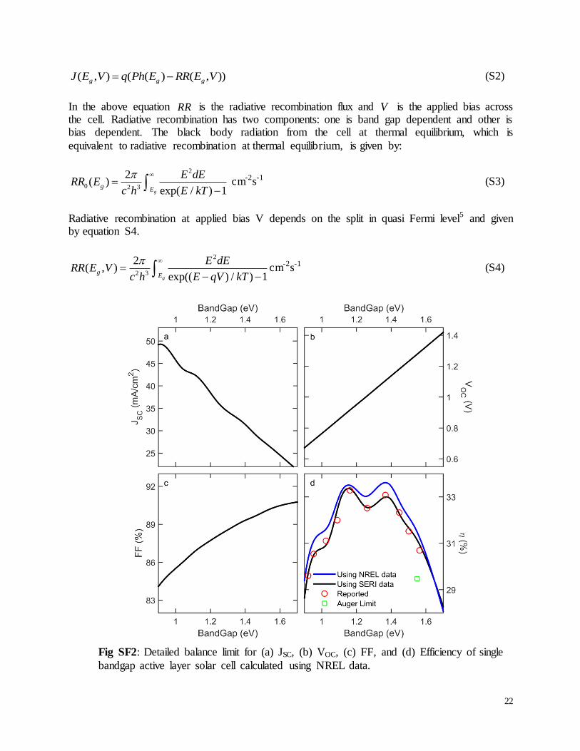
Section I: Detailed balance limit for single active layer solar cell
Detailed balance limit for solar cell was first proposed by Shockley et al.1 and practical limits were further discussed by Green2 and Tiedje et al.3 Using the solar spectrum4 shown in figure
SF1 we calculated the limiting values for different parameters of solar cell as a function of bandgap. For the calculation of limits we assumed that radiative process is the only recombination mechanism in the device as it is fundamental and cannot be avoided if body is at
nonzero temperature. Corresponding plots for the limits are shown in fig SF2.
This detailed balance limit estimate is based on the assumption that solar cell is a perfectly black body for photons of energy more than band gap and white body for photons with energy less than band gap. Based on this assumption we calculated the total number of photons absorbed in
the cell which in turn is equal to the generation rate of electron-hole pairs. If ( )S E is the photon
flux available in solar spectrum for energy E in the energy interval dE then total number of
photons above band gap energy, ( )gPh E , will be,
( ) ( )g
E
gE
Ph E S E dE
. (S1)
All these photons are absorbed by the cell and generate an equal number of electron-hole pairs.
Radiative recombination under black body radiation limit depends on semiconductor temperature
and separation of quasi Fermi levels.5 Any photogenerated e-h pair which does not contribute to the recombination will be extracted from the cell in the form of current. So net current density,
J , obtained from the cell will be
Fig SF1: Global solar irradiance as reported by NREL.
22
( , ) ( ( ) ( , ))g g gJ E V q Ph E RR E V (S2)
In the above equation RR is the radiative recombination flux and V is the applied bias across the cell. Radiative recombination has two components: one is band gap dependent and other is bias dependent. The black body radiation from the cell at thermal equilibrium, which is
equivalent to radiative recombination at thermal equilibrium, is given by:
2
0 2 3
2(
exp( / ) 1)
gg
E
dE
c
E
khRR E
E T
cm-2s-1 (S3)
Radiative recombination at applied bias V depends on the split in quasi Fermi level5 and given by equation S4.
2
2 3
2( , )
exp(( ) / ) 1gg
E
ERR E V
E qV
dE
c h kT
cm-2s-1 (S4)
Fig SF2: Detailed balance limit for (a) JSC, (b) VOC, (c) FF, and (d) Efficiency of single
bandgap active layer solar cell calculated using NREL data.

23
For any semiconductor if applied bias is less than OCV and band gap is more than ~ 0.2 eV, then
qV E on the scale of kT . Therefore eq. S4 can be reduced to
0( , ) ( exp( / ))g gRR E V RR E qV kT (S5)
When cell is in thermal equilibrium then recombination is balanced by generation in the cell. Therefore net recombination in the cell more accurately can be written as
0 0( , ) ( exp( / )) ( )g g gRR E V RR E qV kT RR E (S6)
Using eq. S2 and S6, illuminated JV for the cell can be given by
0( ( ( ( (exp( / ) 1) ) ) ), )g g gJ E q Ph E RR E qV kTV (S7)
Maximum available short circuit current density, )(SC gJ E , for a semiconductor with band gap
gE is ( )gqPh E while open circuit voltage )(OC gV E is the voltage when ,( ) 0gJ E V . Therefore
maximum available )(OC gV E can be given by,
0
)) ln 1
)
(( ~
(( )g
OC g
g
Ph EkTV E
q RR E , (S8)
which is purely a function of bandgap and temperature for a given solar flux. Power ( P )
generated by cell is the product of J and V . Maximum value of power ( MPPP ) was calculated
numerically. Ratio of mppP to the product of )(SC gJ E and )(OC gV E is the fill factor ( )( gFF E ) of
the cell. Efficiency of the cell is given by ratio of )(mpp gP E to the power incident on the cell ( inP
). The detailed balance limit estimates are shown in Fig SF2. SCJ , OCV , and FF as a function of
band gap of semiconductor under radiative limit are shown in part (a), (b), and (c) respectively.
Part (d) shows the variation of efficiency as a function of band gap. Here we provide two estimates, one using the latest NREL4 data for solar spectrum and the other using SERI6 data,
which was used by Tiedje et al.3 The estimates from Tiedje et al are also provided in the same figure (symbols). This shows that our calculations reproduce literature results for the same input solar spectra. For the main manuscript, we have used calculations based on the NREL data.
Section II: Effect of Auger recombination
We also performed auger recombination limit study using the method provided in Tiedje et al.3 For 300 nm thick active layer perovskite solar cell Auger recombination brings the efficiency
down by ~2% (see fig SF2 part d). A similar analysis for Si solar cell was done by Green2 and for GaAs solar cells was reported by Sandhu et al7. The Auger recombination was calculated
under the assumption that n p . The auger recombination rate in the device will be given by
Fig SF2: Detailed balance limit for (a) JSC, (b) VOC, (c) FF, and (d) Efficiency of single
bandgap active layer solar cell calculated using NREL data.

24
0
2( )( )W
iRA A np n n p dx (S9)
Where W is the thickness of active layer, A is the auger recombination coefficient (assuming electron and hole Auger recombination coefficients are same), n and p are the electron and
hole concentration respectively. Under Boltzmann’s a roximation, product of n and p as a
function of voltage is given by
2 exp( )i
qVnp n
kT (S10)
When n p and 2
inp n eq. S9 reduces to
3 32 exp
2( )i
qVRA An W
kT (S11)
Equation S11 is used to get the Auger recombination flux and net J V characteristics is given by
( , ) ( ( ) ( , ) ( , ))g g g gJ E V q Ph E RR E V RA E V (S12)
The new set of solar cell parameters can now be calculated using the J V characteristics obtained from eq. S12.
For 6109in cm-3 and 2911 0A cm6s-1, the performance parameters are 27.3SCJ mA/cm2,
1.17OCV V, 92.34%FF , 29.48% . One order increase in in reduces the efficiency to
26.31% with 27.3SCJ mA/cm2, 1.05OCV V, and 91.73%FF , while one order decrease in
in increases the efficiency to 31.4% with 27.3SCJ mA/cm2, 1.27OCV V, and 90.75%FF .
Similarly for 6109in cm-3, one order change in A from 291 10 cm6s-1 results 1% change in
efficiency mainly through change in OCV .
Section III: Theoretical estimate for radiative recombination coefficient
Detailed numerical simulation of the performance of a solar cell requires the knowledge of recombination parameters for the material used in the cell. Hence for a perovskite solar cell, we
need an estimate of the radiative recombination coefficient. We extracted this value theoretically using the well-known Van Roosbroeck8 model. According to this model, at thermal equilibrium, rate of radiative recombination of electron-hole pair should be equal to rate of generation of
electron-hole pairs by thermal radiation. Therefore radiative recombination in thermal equilibrium can be written as
( )( ) dR P

25
Where ( )P is the probability that a photon of frequency in the frequency interval d will be
absorbed in the unit volume and ( ) is the density of photons with frequency available in
that unit volume.
Roosbroeck et al.8 has shown that above equation can be simplified to 2 3
22 4 3 11.785 ( / 300)1
10g
uE
n duuR cT s
em
T= temperature on absolute scale
/u Th k n= refractive index
= extinction coefficient
gE = band gap of material
Using this equation radiative recombination can be calculated at thermal equilibrium. Also 2
iCn
gives the radiative recombination in thermal equilibrium9 where C is the radiative
recombination coefficient and in is intrinsic carrier concentration in the semiconductor. Using
reported values of refractive index and extinction coefficient for perovskite10 with in of the order
of 69 10 cm-3 we obtained
132 10C cm3/s. Section IV: Simulation methodology and parameters used for simulation
To explore the dark and light JV characteristics, self consistent numerical solution of continuity, charge transport, and Poission’s equation was done using synopsis device simulation tool,
Sentaurus11. The generalized form of these equation are given below, where stands for charge
particle (electron or hole).
Continuity equation: This equation accounts the effect of generation (G ) and recombination ( R )
of carrier density at point x inside the cell on the current density ( J ). Mathematically, the steady state form of continuity equation can be written as,
1( ) ( )
dJG x R x
q dx
(S13)
Negative sign in equation S13 stands for electron and positive sign for holes. q is the charge on
electron Charge transport equation: This equation connects the diffusive and drift component of current
density.
1 dnJ D n E
q dx
(S14)
Negative sign in equation S14 stands for holes and positive sign for electrons. Poisson’s equation: The effect of charge carrier concentration on the electric field/electrostatic
otential is governed b Poisson’s equation given below.

26
0
( )d q
dxx
E
(S15)
Where ( )x is the density of charge carrier at point x . The parameter space used for the
solution of these equation is provided in Table S1.
Table S1: Parameters used for the simulation of perovskite solar cell
Parameter Symbol Unit Perovskite ETL HTL
Electron affinity eV -3.8 -4.0 -2.15
Band gap gE eV 1.55 3.2 3.0
Effective DOS for electron CN cm-3 201 10
201 10 201 10
Effective DOS for hole VN cm-3 201 10
201 10 201 10
Mobility of electron e cm2/V-s 0.2 0.017 0.04*
Mobility of hole h cm2/V-s 0.2 0.017* 0.04
SRH lifetime e h s 62.73 10 - -
Radiative recombination coefficient C cm3s-1 113 10 - -
Auger recombination coefficient n pA A cm6s-1 291 10 - -
Contact work-function eV - -4.2 -4.95
[*Note: electron mobility in HTL or hole mobility in ETL are chosen arbitrarily. However
because of large barriers carriers cannot crossover and these values do not have any effect on simulation results.]
Section V: ideality factor and voltage exponent of
base case simulated device
We have previously shown that perovskite solar cell exhibit two universal features, a) diode ideality factor
is two at low bias and b) voltage exponent is two at high bias12. We find that in present case also, where
radiative recombination and Auger recombination have also been included, same characteristic features are still available (Fig. SF3).
Fig SF3: base case device shows low bias
ideality factor 2 and space charge limited
current at high bias in dark

27
Section VI: Effect of contact layer mobility on the performance of device
As discussed in the main text that performance of the cell can be improved by using high mobility contact layers, our detailed numerical simulation also indicates the same (Fig SF4). It is
clear that increasing the mobility of ETL/HTL could improve the performance, but it is still far below the detailed balance limit. Superposition also does not hold if mobility values for carriers are high in contact layers but not doped. Also if the charge carrier mobility in contact layers is
more than carrier mobility in perovskite, then the performance does not improve any further. Figure SF4 shows the improvement in device performance when e-h mobility in ETL and HTL
are increased.
Section VII Difference in analytical and simulation practical limit of efficiency
As discussed in the main text, the assumption of n p is not valid near the maximum power
point conditions (see Fig. SF5). It leads to higher recombination in practical device as compared
to the detailed balance analysis and reduces the open circuit voltage. Figure SF5b shows a comparison of the generation rate and recombination rate (from both detailed balance analysis
and simulation) integrated over the thickness of perovskite layer. It is evident that the recombination in an actual device is more as compared to same in detailed balance analysis. As a
consequence, the OCV of the device is a lower than the corresponding detailed balance limit. In
addition, voltage at maximum power point ( MPPV ) is also different, which are indicated by points
A (1.087 V from numerical simulations) and B (1.097 from detailed balance analysis) in figure
Fig SF4: Effect of mobility of contact layers on the performance of the cell. Failure of superposition can be observed by the difference in curve obtained from simulation
(line with squares) and superposition (line with cross).

28
SF5b. Increased recombination in simulation lead to some difference in MPPJ also. However, this
difference is very small but it also contributes to efficiency difference. The inset of SF5b clearly
indicates that net recombination in simulation result is little higher than analytical result.
Consequently the MPPJ for simulation is lower than analytical
MPPJ . The efficiency of solar cell
is given by
100MPP MPP
in
J
P
V
Differentiating both side lead to
MPP MPP
MPP MPP
J V
J V
( )ana ana
MPP MPPana
MPP MPPJ V
J V
(S16)
The subscript ana in equation (S16) corresponds to analytical result and represents the
difference in analytical and simulation result. Analytical efficiency of device is 29.48% with
MPPJ and MPPV being 26.87 mA/cm2 and 1.097 V respectively. Corresponding simulation results
are 26.76 mA/cm2 and 1.087 V respectively. Equation (S16), when solved using these values,
yields ~ 0.4% , which is exactly the difference observed in detailed numerical simulations
and analytical calculations.
Figure SF5: Difference in recombination in analytical approach and detailed simulation.
Part a shows the carrier concentration profile inside perovskite for device with optimum efficiency at 1.05 V applied voltage. Recombination profile integrated over perovskite
thickness along with integrated carrier generation rate as a function of applied bias is shown in part b.

29
Section VIII: Performance metrics for different device schemes discussed in main text
Performance change using scheme S1 and S3 are shown in figure SF6. Curve AX shows the performance change using scheme S1 while change for scheme S3 is shown by curve BY. It can be seen that although schemes S1 and S2 were supposed to have potential to improve the
performance but improvement is very less for low doping density while high doping degrades the performance.
Table S2: Parameters for different nodal points in Figure 3b
Point → A B C D E F
C (cm3s-1) 113 10 113 10
113 10 133 10
113 10 133 10
e h (s)
62.73 10 62.73 10
62.73 10 32.73 10 62.73 10
32.73 10
Doping value of
contact layers (cm-3)
- 191 10 191 10
191 10 - -
G (cm-3s-1) 214.48 10
214.48 10
215.67 10
215.67 10
215.67 10
215.67 10
Figure SF6: Performance tradeoff using
different proposed scheme discussed in the
main text. Curve AX shows the performance
variation if scheme S1 is used while BY
shows the performance trend if scheme S3 is
used. Other curves are discussed in main text.

30
Table S3: Performance metrics for different nodal points in Figure 3b
Point → A B C D E F
SCJ 21.5 21.5 27.3 27.3 27.3 27.3
OCV 1.07 1.07 1.08 1.16 1.08 1.16
FF 67.4 84.6 84.8 91.5 65.0 75.8 15.5 19.5 24.9 29.1 19.1 24.0

31
References:
1 S. William and J.Q. Hans, J. Appl. Phys. 32, 510 (1961).
2 M.A. Green, IEEE Trans. Electron Devices 31, 671 (1984).
3 T. Tiedje, E. Yablonovitch, G.D. Cody, and B.G. Brooks, IEEE Trans. Electron Devices 31,
711 (1984).
4 Solar Spectral Irradiance: ASTM G-173, NREL, < http://rredc.nrel.gov/solar/spectra/am1.5/ASTMG173/ASTMG173.html>.
5 W. Ruppel and P. Wurfel, IEEE Trans. Electron Devices 27, 877 (1980).
6 R. Matson, R. Bird, and K. Emery, Terrestrial Solar Spectra, Solar Simulation, and Solar Cell
Efficiency Measurment (Golden, Co, 1981).
7 S. Sandhu, Z. Yu, and S. Fan, Opt. Express 21, 1209 (2013).
8 W. van Roosbroeck and W. Shockley, Phys. Rev. Lett. 94, 1558 (1954).
9 R.N. Hall, in Proc. IEE - Part B Electron. Commun. Eng. (1959), pp. 923–931.
10 C.-W. Chen, S.-Y. Hsiao, C.-Y. Chen, H.-W. Kang, Z.-Y. Huang, and H.-W. Lin, J. Mater. Chem. A (2014).
11 Sentaurus Device Simulation Tool, Synopsys, (2011).
12 S. Agarwal, M. Seetharaman, N.K. Kumawat, A.S. Subbiah, S.K. Sarkar, D. Kabra, M.A.G.
Namboothiry, and P.R. Nair, J. Phys. Chem. Lett. 5, 4115 (2014).