performance analysis of array multiplier using spl...
TRANSCRIPT
Performance Analysis of Array MultiplierUsing SPL and Control Input TechniqueBased Adder Cells for Neural NetworksK. Nehru, M. Ramesh Babu, Seetaiah Kilaru and Shashikanth Reddy
Abstract: In this article presents the investigation of array multipliers using SPL and control input technique basedadder cells. The proposed SPL based adder cell consumes low power, small silicon area and low delay compared tocontrol input technique based adder cell. The proposed circuit is tested with 4 bit array multiplier in terms of power,delay for 45 and 180 nm technology nodes. The array multiplier shows 20 % improvement in power consumptionand 18% improvement in transistor count and these parameters are analyzed using cadence virtuoso software.
Keywords: SPL logic, Control input technique, Array Multiplier, Low Power
1. INTRODUCTION
The ultimate goal of VLSI system is to reduce the energy consumption and silicon area of the systems. Theswitching power component is called as dynamic power dissipation and it is the major source of powerdissipation in systems [11]. The mathematical model of neurons involves the components of arithmetic subsystems in neural architecture. The power optimization of neural network architecture is achieved by lowpower adder and multiplier cell with minimum footprint of the system [10, 3]. The improvement in neuralnetwork is obtained by using SPL based adder cell. The major advantage of single phase logic it requiressmall silicon area compared to all other designs. The SPL adder is designed by using factoring techniquewith small sub circuits.
The DPL gate consists of complementary inputs and outputs and is thus dual rail logic like CPL. Themain idea of double pass transistor logic is both PMOS and NMOS networks are used in parallel. Thesignal degradation is avoided by using double pass transistor logic. There is no level restoration required indouble pass transistor logic [2].
Markovic [5] has discussed several pass transistor logic families like CPL, DPL, and DVL.Complementary pass transistor logic consists of complementary inputs and outputs, a NMOS network. InCPL swing restoration is achieved by use of weak PMOS transistor. The main drawback of DPL logic is itstransistor count. To overcome the problem of transistor count, a new logic family is derived named asDVL. The DVL is mainly used to eliminate redundant branches in double pass transistor logic. Kosonocky[4] proposed a concept called multi threshold techniques to minimize leakage current in the active mode ofoperation. The performance is improved by properly selecting low Vth devices and high Vth devices. Thenew hybrid style full adder circuit was analyzed by the various CMOS logic styles like C-CMOS, CPL,TFA, TGA [6]. Ivakhnenko [7] works on identifying and analyzing systems based on the theory of selforganization have been actively pursued in the field of engineering and technology. The MCIT based addercell decomposition logic is applied for sum expression and pass transistor logic applied for carry expression
* Institute of Aeronautical Engineering, Hyderabad, Email: [email protected]
** Department of Electronics and Communication Engineering.
I J C T A, 8(5), 2015, pp. 2189-2194© International Science Press
2190 K. Nehru, M. Ramesh Babu, Seetaiah Kilaru and Shashikanth Reddy
[1, 12]. A threshold is specified at each level to determine if the outputs of the elements in a layer are givingacceptable results [9].The basic idea of group method of data handling, which is a tool for modeling complexinput-output relationships by building hierarchical polynomial regression networks, was used [7,8].
2. ADDER ARCHITECTURES
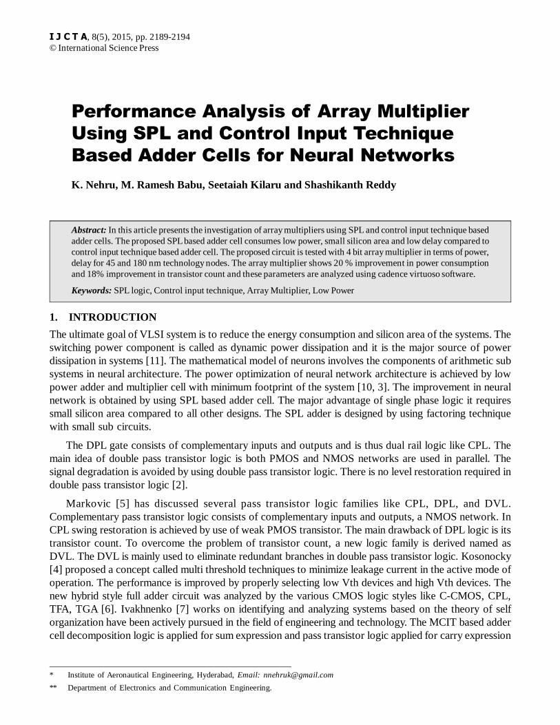
The model of neurons consists of adder and multiplier blocks in shown in figure 1.
Figure 1: Neuron Hardware Structure
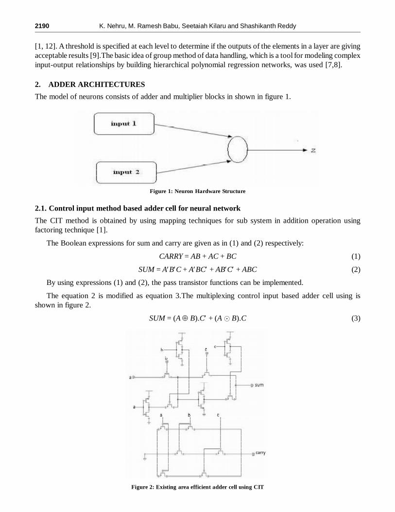
2.1. Control input method based adder cell for neural network
The CIT method is obtained by using mapping techniques for sub system in addition operation usingfactoring technique [1].
The Boolean expressions for sum and carry are given as in (1) and (2) respectively:
CARRY = AB + AC + BC (1)
SUM = A�B�C + A�BC� + AB�C� + ABC (2)
By using expressions (1) and (2), the pass transistor functions can be implemented.
The equation 2 is modified as equation 3.The multiplexing control input based adder cell using isshown in figure 2.
SUM = (A � B).C� + (A ��B).C (3)
Figure 2: Existing area efficient adder cell using CIT
Performance Analysis of Array Multiplier Using SPL... 2191
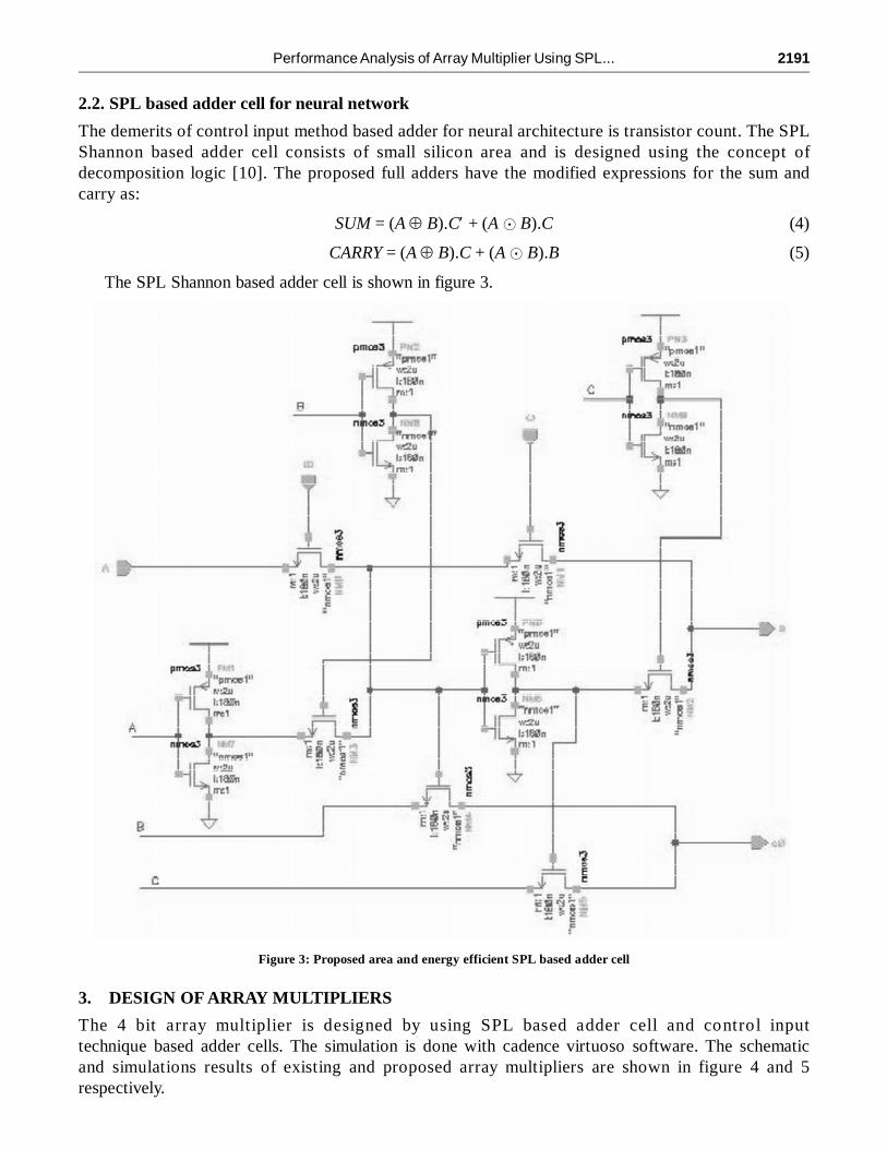
2.2. SPL based adder cell for neural network
The demerits of control input method based adder for neural architecture is transistor count. The SPLShannon based adder cell consists of small silicon area and is designed using the concept ofdecomposition logic [10]. The proposed full adders have the modified expressions for the sum andcarry as:
SUM = (A � B).C� + (A ��B).C (4)
CARRY = (A � B).C + (A ��B).B (5)
The SPL Shannon based adder cell is shown in figure 3.
Figure 3: Proposed area and energy efficient SPL based adder cell
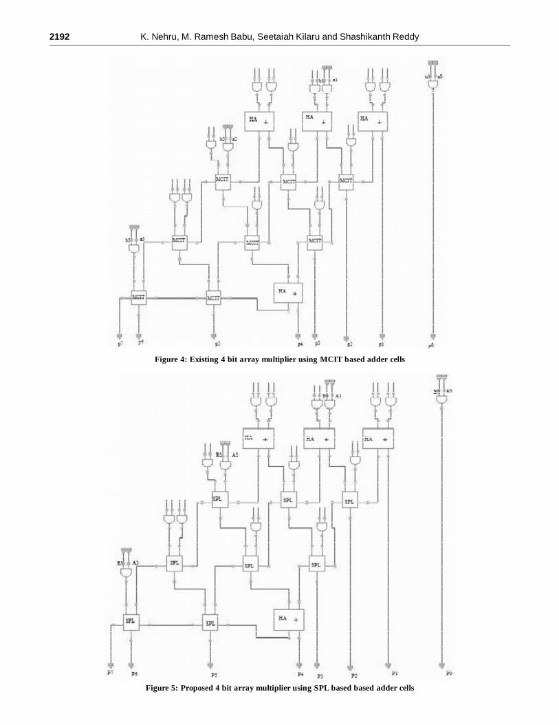
3. DESIGN OF ARRAY MULTIPLIERS
The 4 bit array multiplier is designed by using SPL based adder cell and control inputtechnique based adder cells. The simulation is done with cadence virtuoso software. The schematicand simulations results of existing and proposed array multipliers are shown in figure 4 and 5respectively.
2192 K. Nehru, M. Ramesh Babu, Seetaiah Kilaru and Shashikanth Reddy
Figure 5: Proposed 4 bit array multiplier using SPL based based adder cells
Figure 4: Existing 4 bit array multiplier using MCIT based adder cells
Performance Analysis of Array Multiplier Using SPL... 2193
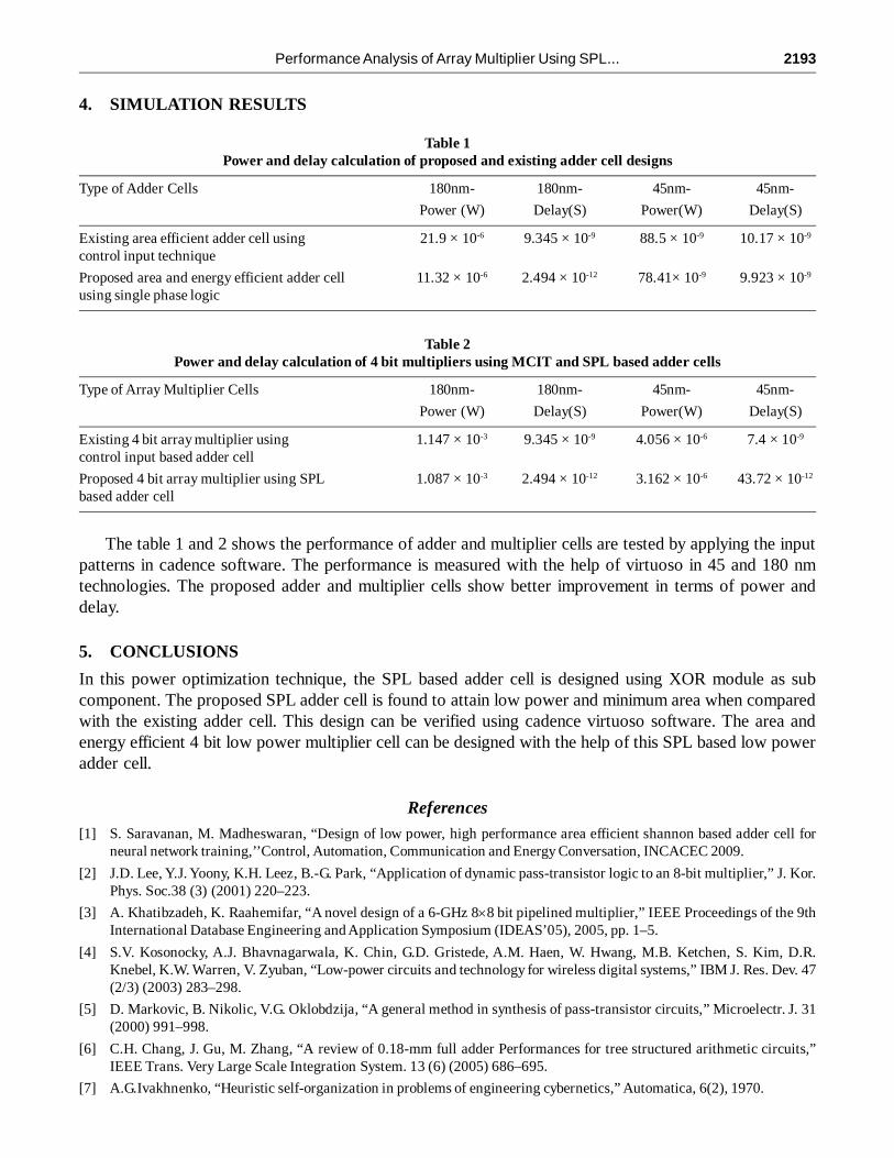
4. SIMULATION RESULTS
Table 1Power and delay calculation of proposed and existing adder cell designs
Type of Adder Cells 180nm- 180nm- 45nm- 45nm-
Power (W) Delay(S) Power(W) Delay(S)
Existing area efficient adder cell using 21.9 × 10⁻⁶ 9.345 × 10⁻⁹ 88.5 × 10⁻⁹ 10.17 × 10⁻⁹
control input technique
Proposed area and energy efficient adder cell 11.32 × 10⁻⁶ 2.494 × 10⁻¹² 78.41× 10⁻⁹ 9.923 × 10⁻⁹
using single phase logic
Table 2Power and delay calculation of 4 bit multipliers using MCIT and SPL based adder cells
Type of Array Multiplier Cells 180nm- 180nm- 45nm- 45nm-
Power (W) Delay(S) Power(W) Delay(S)
Existing 4 bit array multiplier using 1.147 × 10⁻³ 9.345 × 10⁻⁹ 4.056 × 10⁻⁶ 7.4 × 10⁻⁹
control input based adder cell
Proposed 4 bit array multiplier using SPL 1.087 × 10⁻³ 2.494 × 10⁻¹² 3.162 × 10⁻⁶ 43.72 × 10⁻¹²
based adder cell
The table 1 and 2 shows the performance of adder and multiplier cells are tested by applying the inputpatterns in cadence software. The performance is measured with the help of virtuoso in 45 and 180 nmtechnologies. The proposed adder and multiplier cells show better improvement in terms of power anddelay.
5. CONCLUSIONS
In this power optimization technique, the SPL based adder cell is designed using XOR module as subcomponent. The proposed SPL adder cell is found to attain low power and minimum area when comparedwith the existing adder cell. This design can be verified using cadence virtuoso software. The area andenergy efficient 4 bit low power multiplier cell can be designed with the help of this SPL based low poweradder cell.
References[1] S. Saravanan, M. Madheswaran, “Design of low power, high performance area efficient shannon based adder cell for
neural network training,’’Control, Automation, Communication and Energy Conversation, INCACEC 2009.
[2] J.D. Lee, Y.J. Yoony, K.H. Leez, B.-G. Park, “Application of dynamic pass-transistor logic to an 8-bit multiplier,” J. Kor.Phys. Soc.38 (3) (2001) 220–223.
[3] A. Khatibzadeh, K. Raahemifar, “A novel design of a 6-GHz 8�8 bit pipelined multiplier,” IEEE Proceedings of the 9thInternational Database Engineering and Application Symposium (IDEAS’05), 2005, pp. 1–5.
[4] S.V. Kosonocky, A.J. Bhavnagarwala, K. Chin, G.D. Gristede, A.M. Haen, W. Hwang, M.B. Ketchen, S. Kim, D.R.Knebel, K.W. Warren, V. Zyuban, “Low-power circuits and technology for wireless digital systems,” IBM J. Res. Dev. 47(2/3) (2003) 283–298.
[5] D. Markovic, B. Nikolic, V.G. Oklobdzija, “A general method in synthesis of pass-transistor circuits,” Microelectr. J. 31(2000) 991–998.
[6] C.H. Chang, J. Gu, M. Zhang, “A review of 0.18-mm full adder Performances for tree structured arithmetic circuits,”IEEE Trans. Very Large Scale Integration System. 13 (6) (2005) 686–695.
[7] A.G.Ivakhnenko, “Heuristic self-organization in problems of engineering cybernetics,” Automatica, 6(2), 1970.
[8] M.C. Acock, Y.A. Pachepsky, “Estimating missing weather data for agricultural Simulations using group method of datahandling,” Journal of Applied meteorology, 39(2), pp. 1176-1184, 2000.
[9] T.Kondo, A.S.pandya, J.M.Zurada, “logistic GMDH-type notification neural networks and their application to theidentification of the X-ray film characteristic curve, “proc. of IEEE international Conference on System, Man, andCybernetics, pp. 437-442, 1999.
[10] K. Nehru, Dr. A. Shanmugam, S. Deepa and R. Priyadharshini “A Shannon based low power adder cell for neural networktraining”, IACSIT International Journal of Engineering and Technology, Vol. 2, No. 3, pp. 258-262, 2010.
[11] K. Nehru, A.Shanmugam, “Design of high performance low power full adder,” International Journal of Computer applicationin technology, Vol. 49, No. 2, pp. 134-140, 2014.
[12] Rupali Gupta, Mr. Rajesh Mehra, “ Study, Implementation and comparison of different array multipliers using modifiedShannon based adder cell “, International Journal of Electronics Communication and Computer Engineering, Vol. 5,No. 1, 2014.
2194 K. Nehru, M. Ramesh Babu, Seetaiah Kilaru and Shashikanth Reddy