ee 103 lab 3 part 2: 8x8 signed array multiplier for this ... · ee 103 lab 3 part 2: 8x8 signed...
TRANSCRIPT

EE 103 Lab 3 Part 2: 8x8 Signed Array Multiplier Bradley Frizzell, Connor Cunningham
For this lab, an 8x8 Signed Array Multiplier was designed. To begin, a Half Adder was designed, utilizing symbol views of the gates designed in Part 1 of Lab 3. The Half Adder schematic can be seen in Figure 1, and its verified output in Figure 2.
Figure 1: Half adder schematic
Figure 2: Half adder simulation waveform
Then, a Full Adder was designed to base the multiplier off of. The Full Adder was again based off of the gates designed using Verilog in part 1 of Lab 3. The schematic of the FA can be seen in Figure 3, and the correct waveform output is seen in Figure 4.
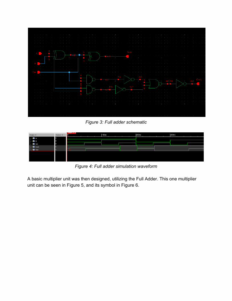
Figure 3: Full adder schematic
Figure 4: Full adder simulation waveform
A basic multiplier unit was then designed, utilizing the Full Adder. This one multiplier unit can be seen in Figure 5, and its symbol in Figure 6.

Figure 5: Multiplier block schematic
Figure 6: Multiplier block symbol

Finally, the one bit multiplier unit was used to create an 8 x 8 array of multipliers, to achieve 8x8 bit multiplication. This design can be seen in Figure 7.
Figure 7: 8x8 signed array multiplier schematic
Once the 8x8 multiplier design was finished, the following 4 equations were tested to verify correct operation, and delays for each were recorded.
1.0111 1111 * 0000 0001 = 0000 0000 0111 1111 a.Delay = 60 ns
2.1000 1111 * 0111 1111 = 0100 0110 1111 0001 a.Delay = 225 ns
3.1000 0000 * 0000 0001 = 0000 0000 1000 0000 a.Delay = 75 ns
4.0111 1111 * 1000 1111 = 0100 0110 1111 0001 a.Delay = 200 ns

Figure 8: 8x8 signed array multiplier simulation waveform
(0111 1111 * 0000 0001 = 0000 0000 0111 1111)
Figure 9: 8x8 signed array multiplier simulation waveform
(1000 1111 * 0111 1111 = 0100 0110 1111 0001)
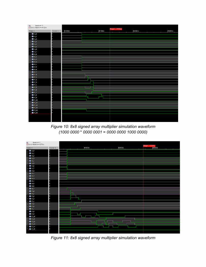
Figure 10: 8x8 signed array multiplier simulation waveform
(1000 0000 * 0000 0001 = 0000 0000 1000 0000)
Figure 11: 8x8 signed array multiplier simulation waveform

(0111 1111 * 1000 1111 = 0100 0110 1111 0001)
Figure 12: 8x8 signed array multiplier simulation waveform
(1ns pulse to determine prop. delay = 88ns)
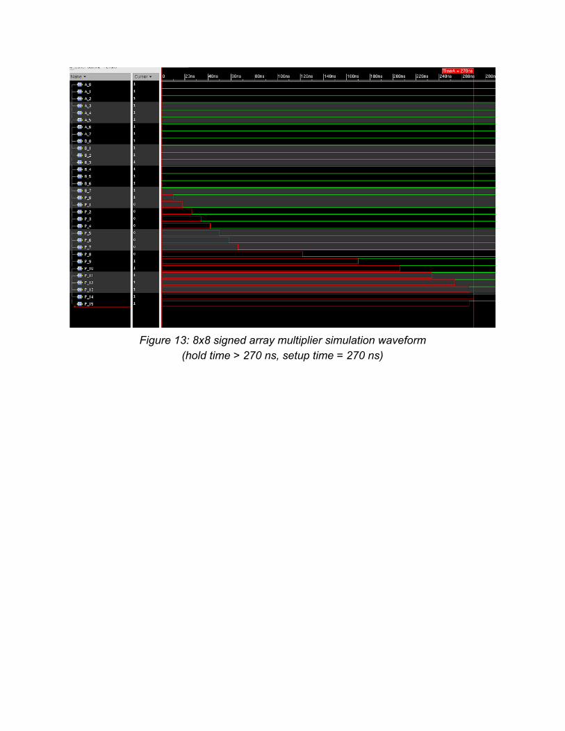
Figure 13: 8x8 signed array multiplier simulation waveform
(hold time > 270 ns, setup time = 270 ns)