power optimization of 4x4-bit pipelined array multiplier · power optimization of 4x4-bit pipelined...
TRANSCRIPT

Power Optimization of 4x4-Bit Pipelined Array Multiplier
Author: Yaseer A. Durrani Supervisor: Teresa Riesgo
Universidad Politécnica de Madrid División de Ingeniería Electrónica
Escuela Técnica Superior de Ingenieros Industriales
(Oct, 2004)

Power Optimization of 4x4-Bit Pipelined Array Multiplier
2
Abstract In this paper, we presented a feasible method of pipelined 4x4-bit array multiplier and evaluated the results by the flexible estimation methods, gate simulation or register-annotated simulation. The multiplier architecture is for low power and high speed applications. The experimental results indicated that this internal optimization reduced the power consumption of this circuit effectively. 1. Introduction As the scale of integration keeps growing, more and more sophisticated signal processing systems are being implemented on a VLSI chip. These signal processing applications not only demand great computation capacity but also consume considerable amount of energy. While performance and area remain to be two major design goals, power consumption has become a critical concern in today’s system design. The need of low power VLSI systems arises from two main forces. First, with the steady growth of operating frequency and processing capacity per chip, large current has to be delivered and the heat due to large power consumption must be removed by proper cooling techniques. Second, battery life in portable electronic devices is limited. Low power design directly leads to prolonged operation time in these portable devices. Multiplication is a fundamental operation in most signal processing algorithms [1]. Multipliers have large area, long latency and consume considerable power. Therefore, low power multiplier design has been an important part in low power VLSI system design. There has been extensive work on low power multipliers at technology, physical, circuit and logic levels. These low-level techniques are not unique to multiplier modules and they are generally applicable to other types of modules. The characteristics of arithmetic computation in multipliers are not considered well. Moreover, power consumption is directly related to data switching patterns. However, it is difficult to consider application-specific data characteristics in low-level power optimization. This dissertation addresses high-level optimization techniques for low power multipliers. High-level techniques refer to algorithm and architecture level techniques that consider multiplication’s arithmetic features and input data characteristics. The main research hypothesis of this work is that high-level optimization of multiplier design produces more power-efficient solutions than optimization only at low-levels. Specifically, we consider how to optimize the internal algorithm and architecture of multipliers and how to control active multiplier resource to match external data characteristics. The primary objective is power reduction with small area and delay overhead. By using algorithms or architecture, it is even possible to achieve both power reduction and area/delay reduction, which is strength of high-level optimization. The trade-off between power, area and delay is also considered in some cases. Innumerable schemes have been proposed for realization of this operation. In the early multiplier schemes proposed by Guilt [2], De Mori [3], Noaks and P. Burton [4] for positive numbers, and by Hwang [5] Baugh and Wooley [6] for numbers in two’s complement form, the effort was on connections pattern. The basic idea behind all these attempts was the fast implementation of the addition of the partial products. For this purpose, the carry-save addition (CSA) technique has been extensively used. In this technique, intermediate results are always in a redundant form of two numbers. Two

Power Optimization of 4x4-Bit Pipelined Array Multiplier
3
types of arrays have been proposed for the addition of the intermediate results. In the first type, the arrays are iterative with regular interconnection structure, permitting multiplication in time )(nO [7], [8]. The second type arrays are of tree form, permitting higher speed in )(log nO time, but the irregular form of a tree-array does not permit an efficient VLSI realization [9]. Modern multiplier designs use [4:2] adders to reduce partial products (PPR) logic delay and regularize the layout. To improve regularity and compact layout, regularly structured tree (RST) with recurring blocks [10] and rectangular-styled tree by folding [11] were proposed, at the expense of more complicated interconnects. In [12], three dimensional minimization (TDM) algorithm was developed to design adder of the maximal possible size with optimized signal connections, which further shortened the (PPR) path by 1~ 2 XOR delays. However, the resulting structure has more complex layout than [4:2] adder based tree. In commercial tools like Power Compiler [13], the gate-level techniques include cell sizing, cell compositions, equivalent pin swapping, and buffer insertion, which produces 11% power reduction on average with 9% area increase [14]. Some other proposed techniques are gate-level signal [15] [16]. At register-transfer level (RTL), clock gating is applied extensively to disable a whole register combinational or sequential blocks not used during a particular period. In Power Compiler [13], clock gating is applied to disable a whole register bank and operand isolation is applied to disable a data-path unit if their outputs are not used. Pre-computation is a RTL signal gating technique which identifies output-invariant logical conditions at some inputs of a combinational block and then disable inputs under these conditions [17]. Retiming re-position registers in sequential circuits so that the propagation of spurious transitions is stopped [18]. At the architecture and system level, there is a great amount of freedom in power optimization. Parallelism and pipeline are two main techniques to first achieve higher-than-necessary performance and then trade operation frequency for supply voltage reduction [19]. Control-data-flow graph (CDFG) transformation is another efficient technique to design low power architecture [20]. Asynchronous systems are investigated to avoid a global clock signal and reduce useless computations [21]. Although optimization techniques at all levels have achieved power reduction, the techniques at the lowest technology level and the highest architecture/system level are generally more efficient than techniques at middle levels. Technology-level optimization affects three important factors LC , DDV and clkf in power consumption. Algorithm/architecture-level optimization affects all three factors. 2. Multiplier Architectures 2.1 Overview The multiplication process may be viewed to consist of the following two steps: evaluation of partial products and accumulation of shifted partial products [20]. The product of two n-digital numbers can be accumulated in n2 digits. In the binary systems, an AND gate can be used to generate partial product iiYX [22]. The evaluation of partial product consists of the logical ANDing of the multiplicand and the relevant multiplier bit. Each column of partial products must be added and, if necessary, values

Power Optimization of 4x4-Bit Pipelined Array Multiplier
4
passed to the next column. In general, the multiplier can be divided into three categories:
1. Serial form 2. Serial/Parallel form 3. Parallel form
The speed of the multiplier is determined by both architecture and circuit. The speed can be expressed by the number of the cell delays along the critical path on the architecture level of the multiplier. The cell delay, which is normally a delay of an adder, is determined by the design of the circuit of the cell. There are three categories of multiplier architectures studied in terms of power consumption:
1. Array Multiplier 2. Tree Multiplier 3. Booth Recoded Multiplier
2.2 Tree Multiplier The multiplication is obtained by first generating partial product and then adding through all of the adders. A full adder, which is the basic addition process usually employed to add two numbers together. If A and B are the adder inputs, and C is the carry input. The full adder produces a bit of summand and a bit of carry out. It can be observed that a full adder is actually a “one’s counter”. The tree multiplier is based on this property of the full adder. Although the tree multiplier has great improvement of speed but the disadvantage of the tree multiplier is the irregular structure as shown in Fig (1). The design time of a tree multiplier is much more than that of a array multiplier. The routing of the signals will be a time-consuming process.
Fig (1) A 4x4-bit Tree Multiplier
2.3 Booth Recoded multiplier The motivation of the Booth Recoded multiplier is that, in case where the multiplier has its 1s grouped into a few contiguous blocks, only a few versions of the multiplicand need to be added to generate the product. If only a few summands need to be added, the multiplication operation can be speed up [22]. Table (1) shows an example of Booth
+
+
+
+
+
+
+
+
+
+
+

Power Optimization of 4x4-Bit Pipelined Array Multiplier
5
recoded algorithm. This technique can be applied to more than two bits simultaneously. Grouping the Booth-recoded selector in pairs Table (2), it is obtain a single, appropriately shifted summand for each pair as shown. The Multiplier 1 1 0 0 0 1 0 1 1 0 1 1 1 1 0 0 The Recoded Multiplier 0 -1 0 0 +1 -1 +1 0 -1 +1 0 0 0 -1 0 0 Bit-Pair Recoding 0 -1 0 -1 +2 +1 0 -1
Table (1) The Multiplier and the Recoded Multiplier by Booth Algorithm [22] The basic idea of the speed up technique is to use bits 1+i and i to select one summand, as a function of 1−i , to be added at summand position i [22]. For a n-bit multiplier, the pair-recoding will generate at most 2/n summands. This is twice as fast as the worst-case original Booth algorithm situation. The advantage of the Booth recoded multiplier is that it avoids the need to correct the product when either input is negative. Bit i+1 Bit i Bit i-1 Version of Multiplicand Selected by bit i
0 0 0 0xM 0 0 1 +1xM 0 1 0 +1xM 0 1 1 +2xM 1 0 0 -2xM 1 0 1 -1xM 1 1 0 -1xM 1 1 1 0xM
Table (2) Booth Multiplier Bit-Pair Recording Table [22]
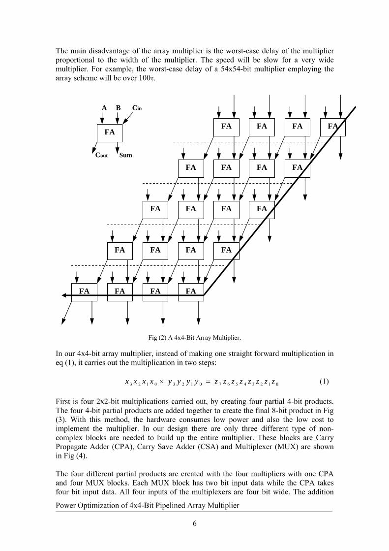
2.4 Array Multiplier The array multiplier originates from the multiplication parallelogram. As shown in Fig (2), each stage of the parallel adders should receive some partial product inputs. The carry-out is propagating into the next row. The bold line is the critical path of the multiplier. In a non-pipelined array multiplier, all of the partial products are generated at the same time. It is observed that the critical path consists of two parts: vertical and horizontal. Both have the same delay in terms of full adder delays and gate delays. For nxn-bit array multiplier, the vertical and the horizontal both have the same delay in terms of full adder delays and gate delays. For an n-bit array multiplier, the vertical and horizontal delays are both the same as the delay of an n-bit full adder. For example a 16x16-bit multiplier, the worst-case delay 32τ where τ is the worse-case full adder delay. The advantage of the array multiplier comes from its regular structure. Since it is regular, it is easy to lay out and has a small size. The design time of an array multiplier is much less than that of a tree multiplier. A second advantage of the array multiplier is its ease of design for a pipelined architecture. A fully pipelined array of the multiplier with a stage delay equal to the delay of a 1-bit full adder plus a register has been successfully designed for high-speed DSP applications at Bell Laboratories [23].
Power Optimization of 4x4-Bit Pipelined Array Multiplier
6
The main disadvantage of the array multiplier is the worst-case delay of the multiplier proportional to the width of the multiplier. The speed will be slow for a very wide multiplier. For example, the worst-case delay of a 54x54-bit multiplier employing the array scheme will be over 100τ.
Fig (2) A 4x4-Bit Array Multiplier.
In our 4x4-bit array multiplier, instead of making one straight forward multiplication in eq (1), it carries out the multiplication in two steps:
0123456701230123 zzzzzzzzyyyyxxxx =× (1) First is four 2x2-bit multiplications carried out, by creating four partial 4-bit products. The four 4-bit partial products are added together to create the final 8-bit product in Fig (3). With this method, the hardware consumes low power and also the low cost to implement the multiplier. In our design there are only three different type of non-complex blocks are needed to build up the entire multiplier. These blocks are Carry Propagate Adder (CPA), Carry Save Adder (CSA) and Multiplexer (MUX) are shown in Fig (4). The four different partial products are created with the four multipliers with one CPA and four MUX blocks. Each MUX block has two bit input data while the CPA takes four bit input data. All four inputs of the multiplexers are four bit wide. The addition
FAFA FAFA
FA FAFAFA
FAFAFAFA
FAFAFA FA
FAFA FA FA
FA
A B
Cout Sum
Cin

Power Optimization of 4x4-Bit Pipelined Array Multiplier
7
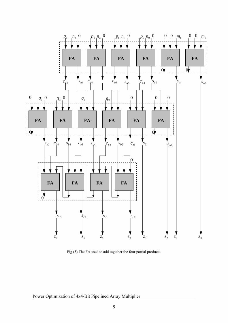
and the carry shift is performed with two CSA and one CPA blocks, which permits the addition of the outputs of the right boundary adders in Fig (4),(8). Each CPA and CSA block has six Full Adders (FA) respectively as shown in Fig (5).
Fig (3) Multiplication Method The full adder (FA) is the most critical circuit in the multiplier as it ultimately determines the speed and power dissipation of the array. A FA is a logic circuit that produces the two-bit sum (Sum and Cout) of three one-bit binary numbers (Cin, x, and y). are in Fig (6) and Table (3). Several of the FA can be reduced to Half Adders (HA) or even no logic at all. The HA circuit and its logical function is shown in Fig (7) and Table (4).
01230101 mmmmxxyy =×
01232301 nnnnxxyy =×
01230123 ppppxxyy =×
01232323 qqqqxxyy =×
0123 mmmm + 0123 nnnn + 0123 pppp + 0123 qqqq
01234567 zzzzzzzz
0123456701230123 zzzzzzzzyyyyxxxx =×

Power Optimization of 4x4-Bit Pipelined Array Multiplier
8
Fig (8) The CPA used to create two products.
Fig (6) A Full Adder Circuit. Table (3) Logical Function of FA. Fig (7) A Half Adder Circuit. Table (4) Logical Function of HA
Inputs Outputs Cin, x,y Cout Sum
0,0,0 0 0 0,0,1 0 1 0,1,0 0 1 0,1,1 1 0 1,0,0 0 1 1,0,1 1 0 1,1,0 1 0 1,1,1 1 1
Inputs Outputs x,y c z 0,0 0 0 0,1 0 1 1,0 0 1 1,1 1 0
FA
x0 0
FA
x1 x0
FA
0 x1
FA
x2 0 0
FA
x3
FA
0 x3 x2
r3 r2 r1 r0 t t2 t1 t0
4 4
4
0
3*x3x2 3*x1x0
x3x2x1x0
XOR
AND
x y
c z
HA
HA
OR Cou Cin
Sum
x y
Power Optimization of 4x4-Bit Pipelined Array Multiplier
9
Fig (5) The FA used to add together the four partial products.
FA
0
0m
0
FA
0
1m
0
FA
0
4ac
5ac
FA
2n
5as
3ac
FA
1p
0
1n
FA
0p
0
0n
3as
3n
3p
2p
0
0
2ac
2as
0
0as
1as
FA
0
0
FA
0
FA
0
4bc
0
FA
0
5bs
3bc
FA
1q
FA
0q
3bs
3q
0
2q
4bs
1bc
2bc
2bs
0
0bs
1bs
FA
0
FA
3cs
FA
FA
2cs
1cs
0
7z
6z
5z
4z
3z
1z
0z
0cs
2z

Power Optimization of 4x4-Bit Pipelined Array Multiplier
10
Fig (4) Full schematics of 4x4-bit Multiplier.
CPA
MUX
MUX
MUX
MUX CSA
CSA
CPA
4
4
4
4
4
4
4
44
6
4
4 2
2 2 2 2
6 4
6
2
4
4
8
3y
2y
2y
3y
1y 0y
1y
4
01234567 zzzzzzzz
0y
Output
Input 0123 xxxx
46

Power Optimization of 4x4-Bit Pipelined Array Multiplier
11
3. Multiplication Algorithm For simplicity, we will describe a basic multiplication algorithm which operates on positive n-bit long integer numbers X and Y resulting in the product P:
∑−
=−− ==
1
0021 2...
n
j
jjnn xxxxX (2)
∑−
=−− ==
1
0021 2...
n
j
jjnn yyyyY (3)
Where 1−nX and 1−nY as the numbers that remain after truncation of bits 1−nX and 1−nY , so
∑−
=−−− ==
2
00321 2...
n
j
jjnnn xxxxX and 1
11 2 −
−− += n
nn xXX (4)
∑−
=−−− ==
2
00321 2...
n
j
jjnnn yyyyY and 1
11 2 −
−− +− n
nn yYY (5)
The product of the numbers X and Y , according to (4) and (5), can be computed as follows: XYP =
{ }{ } { } 111111
111
2211
111
1 2222 −−−−−−−
−−−
−−−
−−− +++=++= nnnnnn
nnn
nnn
nnn
n YXXyYxyxYyXxP (6) If 111 −−− = nnn YXP and generally jjj YXP = (7) Where jX and jY are the numbers formed by the j least significant bits of X and Y , respectively. The jP can be computed by the following recursive equation: If
{ } 1111111
1122 22 −−−−−−
−−−
− +++== jjjjjjj
jjj
jjj YXXyYxyxYXP
{ } 111111
1122 22 −−−−−
−−−
− +++= jjjjjj
jjj
j PXyYxyxP (8) According to the eq (8), the product XYP = can be computed by the equation:
{ }∑ ∑−
=
−
=
++=1
0
1
1
2 22n
j
n
j
jjjjj
jjj yXYxyxP (9)
The main computation concerns the addition of terms jjjjj yXYxZ += (10) These terms must be added, properly weighted, and the product is given by the next relation:
∑ ∑−
=
−
=
+=1
0
1
1
2 22n
j
n
j
jj
jjj ZyxP (11)
The above equation describes a multiplication algorithm that is illustrated in Fig. (8), where the grouping of the partial product bits are distinguished by connecting them with solid lines. By folding the array of this figure along the diagonal line, the final form of the algorithm, given by (11), is derived.

Power Optimization of 4x4-Bit Pipelined Array Multiplier
12
The values that quantity jZ can take depend on the values of the logical variables jx and
jy and are shown in Table (1). The only case where jZ requires computation is when the two bits of the multiplied numbers have value 1. At each step j , only js and 1+jc are new. The rest of the bits of jS have been formed in the previous 1−j steps according to the relation:
Fig (8) Schematic illustration of multiplication algorithm. The values that quantity jZ can take depend on the values of the logical variables jx and
jy and are shown in Table (1). The only case where jZ requires computation is when the two bits of the multiplied numbers have value 1. At each step j , only js and 1+jc are new. The rest of the bits of jS have been formed in the previous 1−j steps according to the relation: 111 −−− ++= jjjj yxSS (12) The sum YXS += can be computed once. During the jth iteration of the algorithm, the j least significant bits of S with jc as the most significant bit form the quality
jS which, in turn, is used only if 1== jj yx . In this case, however, jj cs =+1 and, in algorithm, the quality jS can be computed equivalently by both the following relations: 021 ...ssscS jjjj −−= or 021 ...ssssS jjjj −−= (13) 4. Linear Pipelining Pipeline technique can be applied to the design of the multiplication [24]. A speedup can be easily achieved by implementing the pipeline. A linear pipeline processor is a cascade of processing stages which are linearly connected to perform a fixed function over a stream of data flowing from one end to the other [25].
4y
3y
2y
1y
4x 3x 2x1x 0x
44 yX
33 yX
22 yX
44 xY
33 xY 22 xY0y
3X
2X
3Y 2Y

Power Optimization of 4x4-Bit Pipelined Array Multiplier
13
4.1 Synchronous Model Synchronous pipelines are illustrated in Fig (8. Clocked registers are used to interface between stages. Upon the arrival of a clock pulse, all registers transfer data to the next stage simultaneously. Successive tasks or operations are initiated one per cycle to enter the pipeline. Once the pipeline is filled, one result emerges from the pipeline for additional cycle. This throughput is sustained only if the successive tasks are independent of each other [25].
Fig (9) A Synchronous Pipelined Model. 4.2 Clocking and Timing Control The hold time relates to the delay between the clock input to the register and the storage element. The data has to be held for this period while the clock travels to the point of storage. The setup time is the delay between the data input of the register and the storage element. As the data takes a finite time to travel to the storage point, the clock cannot be changed until the correct data value appears. The delay from the positive clock input to the new value of the register output is called the clock-to-Q delay [25]. The clock cycle τ of a pipeline is determined by the equations below. Let iτ be the time delay of the circuitry in stage si TS , the setup time of the register, and qT the Clock-to-Q delay. Denote the maximum stage delay as mτ , then
1)(max
ki
im ττ = (14)
qsm TT ++= ττ (15) The pipeline frequency is defined as the inverse of the clock period:
τ1
=f (16)
4.3 Speedup Ideally, a linear pipeline of k stages can process n tasks in )1( −+ nk clock cycles, where k cycles are needed to complete the execution of the very first task and the remaining 1−n tasks require 1−n cycles [16]. Thus the total time is [ ]τ)1( −+= nkTk (17) where τ is the clock period. Consider an equivalent-function non-pipelined processor which has a flow-through delay τk . The amount of time it takes to execute n tasks on this non-pipelined processor is τnkT =1 .
Combinational
Logic
Td
Combinational
Logic
Td
Input
Tq Ts Tq
Register Register Register
Output

Power Optimization of 4x4-Bit Pipelined Array Multiplier
14
The speedup factor of a k-stage pipelined over an equivalent non-pipelined processor is defined as
)1()1(
1
−+=
−+==
nknk
nknk
TT
Sk
k τττ (18)
If n is very large, the kSk = where is the number of the pipeline stages. 4.4 Pipelined Multiplier Pipelined multipliers are useful in systems where arithmetic throughput is more important than latency. As discussed in this section, a pipelined multiplier can perform more operations in a certain amount of time and operate with a higher clock rate than a non-pipelined multiplier. The increased throughput does not come without price: the registers used to pipeline the multiplier significantly increase the silicon area taken up by the multiplier. If there are too many pipeline stages, the clock rate of the multiplier will be higher than necessary and the multiplier will take up more area than required. On the other hand, if there are too few pipeline stages, the multiplier will not be able to operate at the system clock rate. To cope with the trade-off, the designer must have a detailed knowledge of the design of the non-pipelined multiplier so that they will know how the pipelining should be done and how fast the resulting circuit will operate. If their knowledge of the circuit is not sufficient, the resulting circuit may not function as expected or will not be optimized for their application. The first concept behind the choice of the architecture is trade-off between area and speed. An optimal system should occupy minimum area but still operated under speed specification. From the discussion of the multiplier architecture (4.2), the smallest architecture of the multiplier is array multiplier. However, it is also slowest architecture. The second concept behind the choice of the architecture is the regularity, which means the design can be divided into several identical sub-modules. By iterating these sub-modules, a system can be easily constructed. The design time is significantly reduced in this way. Extended use may be made of regular structures to simplify the design process. Regularity allows and improvement in productivity by reusing specific designs in a number of places, thereby reducing the number of different designs that need to be completed. Array multipliers satisfy the property of the regularity. The one of the advantages of an array multiplier is regular implementation and minimum area. By inserting one or two pipeline stages into the multiplier, the speed can be significantly improved. The flip-flop reduces the required area of inserting extra pipeline stages. The time of the multiplication should be less than )( Qs TT −−τ , where τ is the clock cycle, sT is the setup time of the output register and QT is the clock-to-Q time of the input register. The number of pipeline stages is determined by the speed of the cell. Pipelining trade increased latency for a higher frequency. It does this by adding register stages. When pipelining a multiplier, the goal is to put half of the multiplier before the added register and the other half of the multiplier after the register shown in Fig (10)
Power Optimization of 4x4-Bit Pipelined Array Multiplier
15
B
A
Clk
D1 Q1
Clk
YD Q
Clk
D2 Q2
Fig (10).Visualizing pipelining.
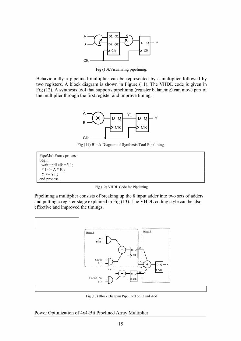
Behaviourally a pipelined multiplier can be represented by a multiplier followed by two registers. A block diagram is shown in Figure (11). The VHDL code is given in Fig (12). A synthesis tool that supports pipelining (register balancing) can move part of the multiplier through the first register and improve timing.
B
A
Clk
D Q
Clk
YD Q
Clk
Y1
Fig (11) Block Diagram of Synthesis Tool Pipelining
PipeMultProc : process begin wait until clk = '1' ; Y1 <= A * B ; Y <= Y1 ; end process ;
Fig (12) VHDL Code for Pipelining
Pipelining a multiplier consists of breaking up the 8 input adder into two sets of adders and putting a register stage explained in Fig (13). The VHDL coding style can be also effective and improved the timings.
Fig (13) Block Diagram Pipelined Shift and Add
AB(0)
A & "0"B(1)
A & "00...00"B(3)
. . .
D Q
Clk
D Q
Clk
YD Q
Clk
Y1
Y2
Stage 2: Stage 1:

Power Optimization of 4x4-Bit Pipelined Array Multiplier
16
The Fig (13) can be simplified as shown in Fig (14).This solution is a balance between getting effective results and coding at a high level.
Clk
D1 Q1
Clk
YD Q
Clk
A
D5 Q5
B
D2 Q2D3 Q3D4 Q4
Y1
Y2
Y3
Y4
Stage 2: Sum
Stage 1: adders per group
Fig (14) Block Diagram for Partial Multiply, Shift and Add.
We implemented a pipelined array multiplier of simple accumulation algorithm by HDL language as shown in Fig (15). Because of the regular circuit architecture in the pipelined array multiplier, we annotated the activities of the registers to evaluate the activities and power consumption of whole circuits. The multiplier can be divided into two pipeline stages as indicated in Fig (15), each of the stage contains the critical path of adders. The introduction of registers along the layer of arrays increase the area of both architectures when compared to non-pipelined architectures in Fig (4). Moreover, the pipelined array multiplier presents the highest area value due to the higher complexity presented by the modules which process the product terms from Table (5). A non-pipelined architecture consumes more power than pipelined multiplier. This occurs because in the pipelined approach glitching is reduced scientifically, and this reduction will have greater impact in the case where the glitching was higher. However, the less logic depth and delay values presented by our architecture still make it significantly more efficient,

Power Optimization of 4x4-Bit Pipelined Array Multiplier
17
Fig (15) 4x4-bit pipelined multiplier.
CPA
MUX
MUX
MUX
MUX
CSA
CSA
CPA
4
4
4
4
4
4
4
4
4
6
4
4 2
2 2 2 2
6 4
6
2
4
4
8
3y
2y
2y 3y
1y 0y
1y
4
01234567 zzzzzzzz
0y
Output
Input 0123 xxxx
46
Registers RegistersRegistersRegisters
Registers Registers Registers
Stage-(1)
Stage-(2)
Power Optimization of 4x4-Bit Pipelined Array Multiplier
18
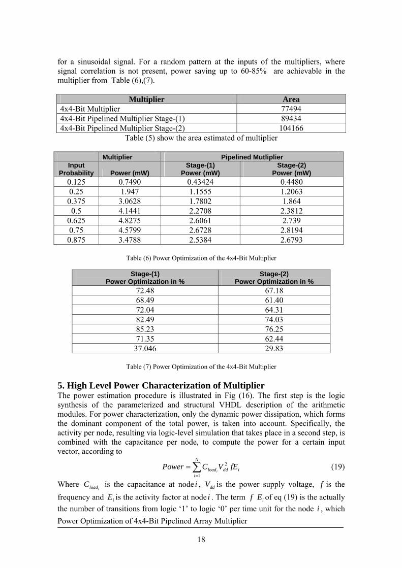
for a sinusoidal signal. For a random pattern at the inputs of the multipliers, where signal correlation is not present, power saving up to 60-85% are achievable in the multiplier from Table (6),(7).
Multiplier Area 4x4-Bit Multiplier 77494 4x4-Bit Pipelined Multiplier Stage-(1) 89434 4x4-Bit Pipelined Multiplier Stage-(2) 104166
Table (5) show the area estimated of multiplier
Multiplier Pipelined Mutliplier Input
Probability Power (mW) Stage-(1)
Power (mW) Stage-(2)
Power (mW) 0.125 0.7490 0.43424 0.4480 0.25 1.947 1.1555 1.2063 0.375 3.0628 1.7802 1.864 0.5 4.1441 2.2708 2.3812
0.625 4.8275 2.6061 2.739 0.75 4.5799 2.6728 2.8194 0.875 3.4788 2.5384 2.6793
Table (6) Power Optimization of the 4x4-Bit Multiplier
Stage-(1)
Power Optimization in % Stage-(2)
Power Optimization in % 72.48 67.18 68.49 61.40 72.04 64.31 82.49 74.03 85.23 76.25 71.35 62.44 37.046 29.83
Table (7) Power Optimization of the 4x4-Bit Multiplier
5. High Level Power Characterization of Multiplier The power estimation procedure is illustrated in Fig (16). The first step is the logic synthesis of the parameterized and structural VHDL description of the arithmetic modules. For power characterization, only the dynamic power dissipation, which forms the dominant component of the total power, is taken into account. Specifically, the activity per node, resulting via logic-level simulation that takes place in a second step, is combined with the capacitance per node, to compute the power for a certain input vector, according to
∑=
=N
iiddload fEVCPower
i1
2 (19)
Where iloadC is the capacitance at node i , ddV is the power supply voltage, f is the
frequency and iE is the activity factor at node i . The term f iE of eq (19) is the actually the number of transitions from logic ‘1’ to logic ‘0’ per time unit for the node i , which

Power Optimization of 4x4-Bit Pipelined Array Multiplier
19
is equal to the ratio of number of node transitions from logic ‘1’ to logic ‘0’, divided by the total number of input vectors:
vectors
transfEf i
i ##
. 0101
→→ == (20)
From eq (19) and (20), the power is:
∑=
→=N
iload
ddii
transCvectorsV
Power1
01
2
##
(21)
The 4x4-bit input modules were simulated with eight different signal probabilities with 1,000 input random vectors. The measurements of power are normalized by frequency, reflecting the fact of simulation, with different operating frequencies.
Fig (16) High level Characterization Flow
6. Conclusions: We have presented a pipelined array architecture multiplier. The structure of this array maintains the same level of regularity as the normal array multiplier. We have presented results that show significant improvement in delay and power. The regularity of our architecture makes it suitable for applying other reducing power techniques. In this work we were able to test the use of pipelining approach in order to reduce the critical path and useless signal transitions that are propagated through the array. As we observed, our multiplier is more efficient due to the logic depth that reduces the amount of glitching along the circuit.

Power Optimization of 4x4-Bit Pipelined Array Multiplier
20
6. References: [1] A. V Oppenheim and R. W Schafer, Discrete-Time Signal Processing. Prentice Hall, 1989. [2] H.Guilt, “Fully Iterative Fast Array for Binary Multiplication”, Electronics Letters, vol. 5, p. 263, 1969. [3] R. De Mori, “Suggestion for an IC Fast Parallel Multiplier”, Electronics Letters, vol 5, p. 50-51, Feb. 1969. [4] P. Burton and D.R. Noaks, “High-Speed Iterative Multiplier”, Electronics Letters, vol. 4, p. 262, 1968. [5] K. Hwang, “Global and Modular Two’s Complement Array Multipliers”, IEEE Trans. Computers, vol. 28, no. 4, pp. 300-306, Apr. 1979. [6] R. Baugh and B.A. Wooley, “A Two’s Complement Parallel Array Multiplication Algorithm, “IEEE Trans. Computers, vol. 22, no. 12, pp. 1,045-1059, Dec. 1973. [7] Y. Oowaki et al., “A Sub-10-ns 16x16 Multiplier Using 0.6-mm CMOS Technology, “IEEE J. Solid-State Circuits, vol. 22, no. 5, Oct. 1987. [8] R. Sharma et al., “A 6.75-ns 16x16-bit Multiplier in Single-Level-Metal CMOS Technology”, IEEE J. Solid-State Circuits, vol. 24, no. 4, Oct. 1989. [9] C. Wallace, “A Suggestion for a Fast Multiplier” IEEE Trans. Electronic Computers, vol. 13, pp. 114-117, Feb. 1964. [10] G. Goto, et. Al., “A 54x54-b regularly structured tree multiplier”, IEEE J. Solid-State Circuits, vol. 27, no. 9, Sept. 1992. [11] N. Itoh, et. Al., “A 600-MHz 54x54-bit multiplier with rectangular-styled Wallace tree” IEEE J. Solid-State Circuits, vol. 36, no. 2, p.249-257, Feb. 2001. [12] V.G. Oklobdzija, D. Villeger, and S.S. Lui, “A method for speed optimized partial product reduction and generation of fast parallel multipliers using an algorithmic approach” IEEE Trans. Compt., vol.45, no.3, pp.249-306, March 1996. [13] Power Compiler Reference Manual. Synopsys, Inc. Nov. 2000. [14] B. Chen and I. Nedelehav, “Power compiler: a gate-level power optimization and synthesis system,” in Proc. 1997 IEEE Int. Conf. Computer Design, pp. 74-79, Oct. 1997. [15] T. Lang, E. Musoll, and J. Cortadell, “Individual flip-flop with gated clocks for low power datapaths,” IEEE Trans. Circuit and Systems II: Analog and Digital Signal Processing, vol. 44, no. 6, pp. 507-516, June 1997. [16] V. Tiwari, S. Malik, and P. Ashar, „Guarded evaluation: pushing power management to logic synthesis/design,“ IEEE Trans. CAD of Integrated Circuits and Systems, vol.17, no. 10, pp.1051-1060, Oct. 1998. [17] M. Alidina, et. al., “Precomputation-based sequential logic optimization for low power,” IEE Trans. VLSI Systems, vol.2, no.4, pp 246-436, Dec. 1994. [18] J. Monteiro , S. Devadas, and A. Ghosh, “Retiming sequential circuits for low power,” in Proc. 1993 Int. Conf. CAD, pp. 398-402, Nov. 1993. [19] A. P. Chandrakasan and R.W. Brodersen, “Minimizing power consumption in digital CMOS circuits,” Proceedings of the IEEE. vol.83, no.4, pp.498-523, Apr. 1995. [20] N. H. E. Weste and K. Eshraghian, Principles of CMOS VLSI Design: a System Perspective, 2nd ed., Addison-Wesley, 1993. [21] M.J.G. Lewis, Low Power Asynchronous Digital Signal Processing, Ph.D. dissertation, University of Manchester, Oct. 2000. [22] V. H. Hamacher, Z. G. Vranesic and S. G. Zaky, Computer Organization, McGraw-Hill, 1990.
Power Optimization of 4x4-Bit Pipelined Array Multiplier
21
[23] M. Hatamian and G. L. Cash, “A 70-MHz 8-bit X 8-bit Parallel Pipelined Multiplier in 2.5-μm CMOS, “IEEE Journal of Solid-State Circuits, Vol. SC-21, No. 4, August 1986. [24] M. R. Satoro and M. A. Horowitz, “SPIM: A pipelined 64x64-bit Iterative Multiplier,” IEEE Journal of Solid-State Circuits, Vol. 24 No. 2, April 1989. [25] Kai Hwang, “Advanced Computer Architecture”, McGraw-Hill, 1993.

Power Optimization of 4x4-Bit Pipelined Array Multiplier
22
7. Appendix: