particle formation during low-pressure chemical vapor
TRANSCRIPT
Particle formation during low-pressure chemical vapor depositionfrom silane and oxygen: Measurement, modeling, and film properties
T. Kim, S-M. Suh, S. L. Girshick, M. R. Zachariah, and P. H. McMurrya)
Department of Mechanical Engineering, University of Minnesota, Minneapolis, Minnesota 55455
R. M. Rassel, Z. Shen, and S. A. CampbellDepartment of Electrical and Computer Engineering, University of Minnesota, Minneapolis, Minnesota 55455
~Received 13 June 2001; accepted 10 December 2001!
Particle generation in thermal chemical vapor deposition~CVD! processes can lead to the formationof contaminant particles that affect film properties and eventually device performance. This articlereports on measurements of particle formation during low-pressure CVD of SiO2 from silane andoxygen. Measurements of aerosol size distributions were made using a particle beam massspectrometer~PBMS! and were carried out at pressures and temperatures ranging from 0.5 to 2.0Torr ~67–267 Pa! and 200–800 °C, using an O2 /SiH4 ratio of 20. We found that within thisparameter space, there are three different particle formation regions and a particle-free region. Theparticle formation regions include an explosion region@200–300 °C,P*1.0 Torr ~;80 Pa!#, anunsteady region@400–600 °C,P*0.8 Torr ~;107 Pa!#, and a steady region@700–800 °C,P*0.6 Torr~;67 Pa!#. PBMS size analysis in the steady region shows that the size distributions arebimodal with one mode around 7 nm in diameter and the other around 20 nm, which is in reasonableagreement with transmission electron microscopy measurements. A numerical model was developedto simulate particle nucleation and growth in this system. The model predicts that for a giventemperature, there exists a critical pressure above which abundant particle formation occurs andbelow which particle production is insignificant. The pressures for which particle formation wasmeasured with the PBMS are in good agreement with model predictions, and measured andcalculated particle sizes are in reasonable agreement. It is also found that there is a correlationbetween particle concentration and film surface morphology, dielectric constant, and current–voltage characteristics of the film. ©2002 American Vacuum Society.@DOI: 10.1116/1.1448506#
cae2
y
aalrinticpavi
sicDs
iotic
a
-less
r tog
iOd-
wothe
oyas-ir–
estry
cht.b-pre-
lm-eac-
I. INTRODUCTION
Contaminant particles formed in semiconductor fabrition processes can lead to a decrease in product yield. A m1% decrease in the product yield can cause more thanloss in profits.1 According to the International TechnologRoadmap for Semiconductors,2 the killer particle size, de-fined as one-half of the gate length, is projected to decreto 50 nm by the year 2005. Such small particles are typicproduced by homogeneous nucleation and growth dufabrication processes. Therefore to meet projected parcontamination control needs, it is essential to understandticle nucleation and growth in the chemically reacting enronments, typical of semiconductor processing.
Low-pressure chemical vapor deposition~LPCVD! can beused to produce various thin films, including poly-Si, SiO2 ,and Si3N4 , and is prone to particle contamination problemWe previously reported on an experimental and theoretstudy of particle nucleation and growth during the LPCVof poly-Si films.3 In extending this work, we chose to focuon particle formation during the LPCVD of SiO2 from SiH4
and O2, since it has the next simplest chemical reactmechanism and it is a natural step towards studies of parformation during plasma-enhanced CVD of SiO2 films,which we plan for the future. Plasma-enhanced CVD h
a!Electronic mail: [email protected]
413 J. Vac. Sci. Technol. A 20 „2…, MarÕApr 2002 0734-2101 Õ200
-re%
selygler-
-
.al
nle
s
largely replaced LPCVD for SiO2 deposition because it provides higher growth rates and step coverages, and isprone to particle contamination.
Despite the fact that LPCVD of SiO2 from SiH4 and O2
has been widely used to provide insulation or as a barrieimpurity diffusion,4 large gaps remain in our understandinof this process: The chemical reaction mechanism of S2
film deposition is not clearly understood and predictive moels for particle nucleation and growth are not available. Tprimary approaches have been employed to describegrowth of silica thin films. These include those that emplphenomenological models that rely on empirical global gphase reactions that are coupled to simple LangmuHinshelwood surface kinetics,5–14 and those that incorporata more molecular description of the vapor phase chemithrough the use of elementary reactions.15–27 Our work isbased on the latter approach.
Only a few studies of particle formation during SiO2
CVD have been reported. Sintaniet al.28 measured the sizedistribution of SiO2 particles during CVD at atmospheripressure by observing Mie scattering of He–Ne laser ligThey found that the size distribution varies with time, sustrate temperature, and reactant concentrations with thedominant particle size in the range of 0.2 to 0.3mm. Theyalso investigated the effect of these particles on ficharacteristics.29 They were unable to find a clear relationship between the presence of gas-borne particles in the r
4132Õ20„2…Õ413Õ11Õ$19.00 ©2002 American Vacuum Society

tho
de
ae
rv
esrnun
uni
threr
teor
tiendprs
turo
pely
he
sn
s as an,erford
n-ns
ainor-
ge-
pri--
icle
,
uf-
solis-
414 Kim et al. : Particle formation 414
tor and the pinhole density or particle contamination offilms. In their experimental study on chemistry and effectselectrical properties of SiO2 films by LPCVD, Liehr andCohen30 varied the reactor temperature and pressure totermine the SiO2 film growth rate. They identified a particlgeneration~powder or snow formation! domain, and theyfound that particles were deposited on the walls of the retor when gas-borne particles were observed. The experimtal conditions used in our study are based on their obsetions. Finally, Whitby and Hoshino31 used their low-pressureaerosol sampler32 to measure the size distribution of particlproduced during LPCVD of SiO2 films. They compared theimeasurements with predictions of their two-dimensionalmerical simulation employing only two gas-phase reactioThey found that particle nucleation rates vary as;P,9 whereP is the total pressure, and that below;5 Torr ~;667 Pa!,particle nucleation rates become negligible. It was also fothat 7 cm above the wafer, the particle size distributiontrimodal with modes at 10, 80, and 110 nm. They arguedthis is because particle nucleation occurs at three diffeplaces:~1! about 2 cm above the center of the wafer, whethe temperature is the highest;~2! about 4 cm above thewafer, where the temperatures are lower; and~3! near theedge of the wafer, where the temperature gradients are s
In this article we report on measurements of particle fmation during LPCVD of SiO2 from SiH4 and O2, and com-pare these results to modeling predictions and film properincluding surface morphology, dielectric constant, acurrent–voltage characteristics. Previous studies havevided little qualitative information on the effects of particleon film properties.
II. EXPERIMENTAL SETUP
A. Gaseous Electronics Conference cell and particlebeam mass spectrometer
Figure 1 shows a schematic of the experimental seused in this study. It consists of inlet gas mass flow contlers, a Gaseous Electronics Conference~GEC! cell,33 the ex-haust pumping manifold, and the particle beam mass strometer~PBMS!.34 The PBMS can sample particles directfrom low-pressure [email protected] mTorr~13 Pa!#, de-tect low particle concentrations~.20 cm23!, and measuresize distributions of ultrafine particles~0.005–0.5mm! in
FIG. 1. Schematic of PBMS and CVD reactor for SiO2 deposition.
J. Vac. Sci. Technol. A, Vol. 20, No. 2, Mar ÕApr 2002
en
e-
c-n-a-
-s.
dsatnte
ep.-
s
o-
pl-
c-
real time. With this technique, particles sampled from tLPCVD reactor are focused by aerodynamic lenses,35,36
charged to saturation by electron impact,37 and classified us-ing an electrostatic energy analyzer.34 A detailed descriptionof this setup is given by Nijhawan.3 Because our experimentinvolved the use of O2 , the filament used within the electrogun described by Ziemann34 had a lifetime of only a fewhours. Therefore we installed a new electron gun which haring-shaped filament made of thoria-coated iridium and halifetime of about 3 months. The design of this electron gushown schematically in Fig. 2, is adopted from the ionizdesign employed in residual gas analyzers made by StanResearch Systems.38 The cathode and filament are maitained at2190 V and the anode at 10 V so that the electrohave 200 eV of energy.
B. PBMS data inversion
In an electrostatic field, the voltage needed to obtenough field strength to deflect incoming particles is proptional to the particle’s kinetic energy-to-charge ratio
V5mu2/2Aze, ~1!
wherem, u, andz are the particle mass, velocity, and char~in elementary units!, respectively.A is a constant that depends on the deflector angle, ande is the elementary electroncharge. Since the particle mass, velocity, and charge aremarily functions of particle size,34 this deflection voltage determines a critical particle size,Dp(V). All particles belowthis critical size are deflected by 90°. The deflected partbeam current measured at the off-axis Faraday detector~Fig.1! is given by
I ~V!5E0
Dp~V! dN
d log~Dp!z~Dp!h~Dp!Qedlog~Dp!, ~2!
wheredN/d log(Dp) is the particle size distribution functionz(Dp) is size-dependent particle charge,h(Dp) is transportefficiency from the PBMS inlet to the 90° deflector, andQ isthe volumetric flow rate. When the deflection voltage is sficiently high to deflect all particles~;300 V!, the particlecurrent provides a measure of the total amount of aerosampled by the PBMS. We can obtain the particle size dtribution function by differentiating Eq.~2!:
FIG. 2. Schematic of new electron gun.

m
ntio
ra
on
anutbn
ndtr
at
io
Mf
usheve
Torra-from-
n
of
manndionrate
thelcu-aremrlyions
e to
te
surera-pres-andera-wase oft theem-werendlossel-d by
-wh -
415 Kim et al. : Particle formation 415
dN
d log~Dp!5
dI
dV
dV
d log~Dp!
1
z~Dp!h~Dp!Qe. ~3!
To get the particle size distribution,I (V) and V(Dp) arerequired.I (V) is obtained by measuring the particle beacurrent while varying the deflecting voltage andV(Dp) isobtained from Eq.~1! using the known relationships betweeparticle size and mass, velocity, and charge. These relaships are explained in detail by Ziemannet al.34 The trans-port efficiency,h(Dp), is almost unity for particles largethan 20 nm, but decreases rapidly as particle size decrebelow 20 nm due to diffusional losses.35,36
C. Experimental conditions
Experiments were performed using an O2 /SiH4 ratio of20, a pressure range from 0.5 to 2.0 Torr~67–267 Pa!, and atemperature range from 200 to 800 °C. These conditiwere determined from previous studies.8,28,30,31Flow rates ofreactant gases were controlled with mass flow controllersthe pressure inside the reactor was controlled by the amatic throttle valve installed in the exhaust line. The sustrate temperature was maintained by using a proportiointegral differential-controlled pyrolitic-graphite heater athe temperature was measured at the center of the subsusing a K-type thermocouple embedded in the substrholder.
III. RESULTS AND DISCUSSION
A. Experimental results
Figure 3 shows the total particle current at a deflectvoltage of 300 V measured during the SiO2 deposition at200 °C at pressures of 1.2 and 1.3 Torr~160 and 173 Pa!. Theactual pressure undergoes small fluctuations at 1.2 Torr~160Pa! and larger fluctuations at 1.3 Torr~173 Pa!, but particlecurrents are one to two orders of magnitude above the PBnoise,;5310214 A. Since the pressure fluctuations can afect the transport efficiency of the particles to the exhaline, it is difficult to correlate the particle generation and tpressure fluctuation. Optical emission was also obserThese pressure fluctuations start at 1.2 Torr~160 Pa! and
FIG. 3. Particle current measured during SiO2 deposition at a substrate temperature of 200 °C. Note the appearance of larger pressure fluctuation,the pressure increased from 1.2 to 1.3 Torr~160–173 Pa!.
JVST A - Vacuum, Surfaces, and Films
n-
ses
s
do--al
atee
n
S-t
d.
become more intense as the pressure is increased to 2.0~267 Pa!. A similar transition from stable to unstable opertion was observed at 300 °C as pressure was increased0.9 to 1.0 Torr~120–133 Pa!. We believe the observed fluctuations are due to explosions within the SiH4 /O2 mixture.Previous work by Hartmanet al.39 showed that for anO2 /SiH4 ratio of 6.1, the lower pressure limit for explosiodecreased from 20 Torr~2.6 kPa! at 60 °C to 5 Torr~667 Pa!at 140 °C. Our observed lower pressure limit of explosion1.2 Torr ~160 Pa! at 200 °C and 1.0 Torr~133 Pa! at 300 °Care consistent with ranges and trends reported by Hartet al. The stability of a mixture for a given temperature apressure with respect to explosion limits is a competitbetween chain branching reactions which serve to accelethe formation of the radical population~H, O, and OH! andchain termination processes which remove radicals. Atpressure and temperature conditions of operations our calations indicate that we are in a regime where explosionsquite probable and for which radical termination results frodiffusional losses to the reactor walls. Indeed, Fig. 3 cleashows that a small increase in pressure results in explos~such as have been observed in the H2 /O2 system40! and isassociated with a decreased radical loss to the walls duthe increased pressure.
Figure 4 shows the particle current~deflection voltage seat 300 V! measured during SiO2 deposition at 500 °C as thpressure was increased from 0.7 to 1.8 Torr~90–240 Pa!.Note that the particle current tends to increase as the presincreases, but fluctuations occur for fixed values of tempeture and pressure, and are more pronounced at elevatedsures. Fluctuations are observed at 400, 500, and 600 °Cgradually disappear as the temperature increases. At temptures above 600 °C, a steady-state particle concentrationachieved as is shown in Fig. 5 for a substrate temperatur800 °C. The reason for the unsteady particle generation aintermediate temperatures is not yet known. Also, as the tperature increases, explosions should occur even at lopressure. The experimental results do not show this trwith increasing temperature and at this point we are at ato explain why. However, it can be speculated that atevated temperatures the showerhead is sufficiently heate
enFIG. 4. Particle current measured during SiO2 deposition at a substrate temperature of 500 °C and pressures changing from 0.7 to 1.4 Torr~93–187 Pa!.

bhstheic
urTohes
ceouTheigcom
veain
entof-e,
end
ofandres
re-
°C
o
nd
ctorlespa-
-
5
5
s.
416 Kim et al. : Particle formation 416
radiative effects that the explosion generating chemistrygins at the exit of the showerhead and is therefore quencdue to its proximity to a radical removal surface. It is posible that at the intermediate temperature range belowtemperature at which all explosions are quenched, thmight exist an unstable reaction domain of unsteady partformation.
Figure 6 shows the particle current while the temperatwas increased from 150 to 800 °C at a pressure of 1.5~200 Pa!, and Fig. 7 shows the particle current while ttemperature was decreased from 800 to 150 °C at a presof 1.5 Torr~200 Pa!. These data provide confirming evidenfor the unsteady and steady particle formation domains. Nthat the explosion domain is not apparent from particle crent data, but was observed from pressure fluctuations.temperature range for these domains is a bit different wwe ramp the substrate temperature up and down. This mbe due to the fact that only the substrate temperature istrolled in this experiment. Thus the temperature of the chaber wall and showerhead tends to lag behind. For a gisubstrate temperature, the average temperature in the rewill tend to be lower when the substrate temperature iscreasing than when it is decreasing.
FIG. 5. Particle current measured during SiO2 deposition at a substrate temperature of 800 °C and pressures changing from 0.6 to 1.8 Torr~80–240 Pa!.
FIG. 6. Particle current measured during SiO2 deposition at a pressure of 1.Torr ~200 Pa! and temperatures changing from 150 to 800 °C.
J. Vac. Sci. Technol. A, Vol. 20, No. 2, Mar ÕApr 2002
e-ed-e
rele
err
ure
ter-henhtn--n
ctor-
Figure 8 summarizes our observations on the differdomains of particle generation during low-pressure CVDSiO2 from SiH4 and O2 as a function of pressure and temperature:~A! a domain of explosion, chemiluminescenclittle particle generation;~B! a domain of unsteady particlgeneration;~C! a domain of steady particle generation; a~D! a domain of no particle generation. Note that the slopethe line, which separates domain of particle generationno particle generation, is determined from the least-squafit of the experimental data shown in Fig. 12.
The PBMS measurements of particle size distributionquire steady-state particle generation~domain C!. Figure 9shows the size distribution for particles generated at 800and 1.5 Torr ~200 Pa!. The distribution is bimodal withmodes,;7 and;20 nm, which is quite small compared t;100 nm reported by McMurryet al.41 This discrepancymight be due to the different reactor configuration aSiH4 /O2 ratio. McMurry et al. used an O2 /SiH4 ratio of1.33 and a horizontal tubular flow reactor~hot-wall type!,which allows longer residence times of gases in the reaand might result in different transport efficiencies of particto the exhaust line. However, our results are quite com
FIG. 7. Particle current measured during SiO2 deposition at a pressure of 1.Torr ~200 Pa! and temperatures changing from 800 to 150 °C.
FIG. 8. Pressure–temperature reaction diagram of the CVD of SiO2 fromSiH4 and O2 . Black dots indicate the conditions at which the films in Fig14–19 were deposited.

ed
ini
edrs
xiswearr
ridaoenwthre
tar-dwtiote
ictrcam
byt byg-ainThene
el.onon
ofases
r.tt
417 Kim et al. : Particle formation 417
rable to those of Whitby and Hoshino,31 who found that thesilicon dioxide particle size distribution is trimodal with thsmallest mode around 10 nm. Although they also usehorizontal tubular flow reactor~cold-wall type!, they em-ployed the same O2 /SiH4 ratio of 20 ~diluted with He! andparticles were sampled directly from the chamber to mmize the particle growth.
Transmission electron microscopy~TEM! was used toverify the PBMS results. Graphite TEM grids were installjust after the skimmer, at the inlet of the second chambethe PBMS~Fig. 1!. Figure 10~a! shows TEM measurementof SiO2 particles generated at 800 °C, 1.5 Torr~200 Pa!. Themajority of the particles are around 10 nm and there esome larger particles around 20–25 nm, which agreeswith the PBMS measurements. Some agglomerates areobserved. To test the hypothesis that agglomeration occuas individual primary particles were deposited on the gwe collected another sample for which particles werepositively charged by the electron gun before they were clected on the TEM grid. In this case, no agglomerates wobserved@Fig. 10~b!#. We believe that electrostatic repulsioprevented the formation of aggregates when this samplecollected. We conclude that particles extracted fromLPCVD reactor consisted of individual particles that wenearly spherical.
B. Comparisons to modeling results
The model employed in this study is described in deelsewhere.42,43 Briefly, four classes of silicon oxide clusteing pathways were considered, based on current knowleof reaction kinetics and cluster properties during lopressure silane oxidation. The species conservation equaand a moment-type aerosol dynamics model were formulafor a one-dimensional stagnation-point flow geometry whsimulates the flow between the showerhead and the subsin a GEC reference cell reactor. The contributing physiand chemical processes considered in the aerosol dyna
FIG. 9. Particle size distribution during CVD of SiO2 from SiH4 and O2 at1.5 Torr ~200 Pa! and a substrate temperature of 800 °C.
JVST A - Vacuum, Surfaces, and Films
a
-
of
tll
lsoed,lll-re
ase
il
ge-nsd
hatelics
model include: homogeneous nucleation; particle growthsurface reactions and coagulation; and particle transporconvection, Brownian diffusion, and thermophoresis. A lonormal particle size distribution was assumed to obtmathematical expressions for the contributing processes.chemical clustering model, together with a detailed silaoxidation mechanism and a SiO2 film growth mechanism,were coupled to the flow and the aerosol dynamics mod
Figure 11 shows the distribution of particle concentratipredicted by our numerical model along the axial directifor reactor pressures ranging from 0.6 to 3 Torr~80–400 Pa!and a substrate temperature of 800 °C. The O2 /SiH4 mixtureenters the reactor at a 20:1 ratio. A dramatic increaseparticle concentration is predicted as the pressure increfrom 0.6 to 0.8 Torr~80–107 Pa!, while the particle concen-
FIG. 10. ~a! TEM micrograph of SiO2 particles generated at 800 °C, 1.5 Tor~Scale bar: 50 nm!. ~b! TEM micrograph of SiO2 particles generated a800°C, 1.5 Torr. The particles shown in~b! are positively charged to prevenagglomeration while they are deposited.~Scale bar: 200 nm!.

hfo
iniO
eura-esb
lena
thstiic
pub
sentless use-par-ratetrate-ter-
rceande inne-
ticuchngctor
terandear-ev-beinceres-
rzes
ns
well-ur
ar-theunt
as
iou
dt
ious
418 Kim et al. : Particle formation 418
tration becomes relatively insensitive to pressure at higpressures. Our model assumes that silicon oxide particlemation in this system is largely attributable to the clusterreactions among a few gas species, which include SiO, S2 ,HSiOOH, and SiH2O. At pressures below 0.8 Torr~107 Pa!,diffusion prohibits local accumulation of the clustering spcies, thereby suppressing particle formation. For pressabove 0.8 Torr~107 Pa!, particle generation becomes reltively insensitive to pressure since diffusion becomes lsignificant at high pressures. We believe this behavior touniversal in nature, based on a recent nondimensionanalysis of particle nucleation in a convection-diffusion evironment where we discovered a critical total pressurewhich cluster diffusion leads to a dramatic decrease inparticle production rate. These results imply that changetotal reactor pressure, even when the precursor concentrais held constant, can lead to significant changes in partproduction.
Figure 12 compares the observed onset pressures ofticle generation with the model predictions at various s
FIG. 11. Calculated particle concentration generated at 800 °C for varprocessing pressures.
FIG. 12. Comparison between onset of particle generation detectedPBMS and predicted by modeling work. The solid line represents moresults and the squares represent measurements. ‘‘Dirty wafer’’ meansthe model predicts that particles will deposit on the wafer.
J. Vac. Sci. Technol. A, Vol. 20, No. 2, Mar ÕApr 2002
err-
g
-es
sess-teinonle
ar--
strate temperatures. The experimental data points reprethe minimum pressure at which the PBMS detected particat a given substrate temperature. Our model also enableto calculate the particle flux to the wafer. A clean wafer rgion is predicted at higher substrate temperatures whereticles are thermophoretically pushed away from the substat lower pressures. As the pressure increases, the substemperature-induced thermophoretic force becomes counbalanced and finally dominated by the thermophoretic foinduced by the exothermicity of the gas-phase chemistryby the increased particle generation due to the increaspartial pressure of precursor species. Note that this odimensional~1D! model does not account for thermophoretransport to the reactor side walls. As we discuss later, sradial transport may play an important role in determiniwhether particles are deposited on the wafer or on the reawall.
Figure 13 shows the variation in particle median diamealong the axis of the reactor for a temperature of 800 °Cthe same range of pressure as in Fig. 11. As mentionedlier, the model assumes a log-normal size distribution atery axial location. The median particle size is predicted toless than 10 nm for the range of pressures considered. Sthe predicted median sizes of the particles generated at psures below 1.5 Torr~200 Pa! are smaller than the lowelimit of detection of the PBMS, measured and predicted siof the particles generated at 1.5 Torr~200 Pa! are compared.As was shown in Fig. 9, bimodal particle size distributiowere measured at the exhaust line at 1.5 Torr~200 Pa!. Themeasured size of the first mode, 7 nm, agrees reasonablywith the predicted particle size,;6 nm, considering that additional growth, not accounted for in the model, might occas particles travel from the chamber to the exhaust line.
The second mode in Fig. 9 is most likely due to the pticle nucleation in a region other than the region betweenshowerhead and the wafer. Our 1D model does not accofor such processes. Whitby and Hoshino31 argued that theobserved trimodal particle size distribution in their study w
s
byelhat
FIG. 13. Calculated particle median diameter generated at 800 °C for varprocessing pressures.
ee
ssd
ceaioree
olortinit-
sulen
en
nra-
ickOhes of
edntdedpro-
inlmsasingin
ause
419 Kim et al. : Particle formation 419
due to the fact that particle nucleation takes place both nthe center of the wafer and near its edge, where the tempture gradients are steep. It is possible that similar proceoccur in our system and are responsible for the larger moHowever, it is also possible that the larger mode is produby particles that are formed upstream of the showerhewhere we have observed a residue of particle depositSiH4 and O2 gases, supplied through two different lines, amixed before they enter the chamber through the showhead, which consists of 169 equally spaced concentric h~305 mm! drilled in a circular disk. The showerhead interiis maintained at a constant temperature using circulachilled water, but due to radiation from the substrate,temperature can increase to;200 °C when the substrate temperature is 800 °C. The elevated temperatures and presupstream of the showerhead may promote reactions thatto nucleation that are not accounted for in our model awhich may be responsible for the larger mode.
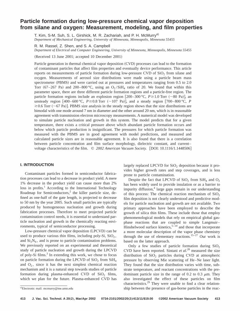
FIG. 14. Atomic force micrograph of SiO2 film deposited at 1.0 Torr~133Pa! and 300 °C.
FIG. 15. Atomic force micrograph of SiO2 film deposited at 0.6 Torr~80 Pa!and 500 °C.
JVST A - Vacuum, Surfaces, and Films
arra-ese.dd,n.
r-es
gs
resadd
C. Comparisons to film property measurements
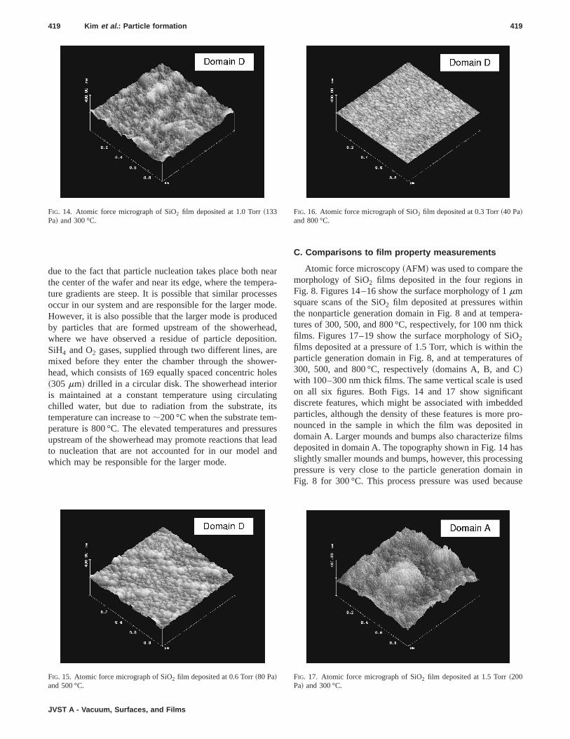
Atomic force microscopy~AFM! was used to compare thmorphology of SiO2 films deposited in the four regions iFig. 8. Figures 14–16 show the surface morphology of 1mmsquare scans of the SiO2 film deposited at pressures withithe nonparticle generation domain in Fig. 8 and at tempetures of 300, 500, and 800 °C, respectively, for 100 nm thfilms. Figures 17–19 show the surface morphology of Si2
films deposited at a pressure of 1.5 Torr, which is within tparticle generation domain in Fig. 8, and at temperature300, 500, and 800 °C, respectively~domains A, B, and C!with 100–300 nm thick films. The same vertical scale is uson all six figures. Both Figs. 14 and 17 show significadiscrete features, which might be associated with imbedparticles, although the density of these features is morenounced in the sample in which the film was depositeddomain A. Larger mounds and bumps also characterize fideposited in domain A. The topography shown in Fig. 14 hslightly smaller mounds and bumps, however, this processpressure is very close to the particle generation domainFig. 8 for 300 °C. This process pressure was used bec
FIG. 16. Atomic force micrograph of SiO2 film deposited at 0.3 Torr~40 Pa!and 800 °C.
FIG. 17. Atomic force micrograph of SiO2 film deposited at 1.5 Torr~200Pa! and 300 °C.

satte
arghfilmfily
infe
odedchhaonanhtn
os-ig-m-ralra-
culergyeFig.eld
tor-
lm,aci-
odeVDo-
Sius tohendby
t
ntes
re-
420 Kim et al. : Particle formation 420
very little film deposition was observed at 300 °C for presures below 1 Torr. Comparing Figs. 15 and 18, a dramroughening of the surface is observed when processing inunsteady particle generation domain B. The structures sin Fig. 17 are still seen in Fig. 18, but the structureslarger with higher densities. Finally, comparison of the hitemperature images in Figs. 16 and 19 shows that theseare dramatically different in roughness and features. Thedeposited in domain C~Fig. 19! has an extreme topographwhile the corresponding film in domain D~Fig. 16! issmooth. All of the images obtained from films depositedthe particle generation domain show large and roughtures.
To get a more quantitative measure of the surface topraphy, a 10310mm2 region was scanned on the AFM anthe rms roughness measured. The results are summarizTable I. As expected, the film shown in Fig. 18 is murougher than the film shown in Fig. 15. Less obvious is tthe film in Fig. 17, which was deposited in the explosiparticle generation domain A, is significantly rougher ththe film deposited at the same temperature but at a sliglower pressure, despite the pressure in that case being
FIG. 18. Atomic force micrograph of SiO2 film deposited at 1.5 Torr~200Pa! and 500 °C.
FIG. 19. Atomic force micrograph of SiO2 film deposited at 1.5 Torr~200Pa! and 800 °C.
J. Vac. Sci. Technol. A, Vol. 20, No. 2, Mar ÕApr 2002
-icheene
sm
a-
g-
in
t
lyear
the particle generation domain. Figure 19, which was depited in the steady state particle production region C, is snificantly rougher than the film deposited at the same teperature but within the nonparticle regime. Also, the genereduction of roughening with increasing deposition tempeture seen in Figs. 14–16 is not surprising. Since SiO2 isamorphous, increasing temperature increases admolemobility without faceting. This increased admolecule eneshould lead to film smoothing by surface diffusion. Throughness measurements seem to confirm the outline of8, even though this result is less obvious on the small fiscans.
If particles are embedded in the films, they are likelyaffect electrical properties of the film as well as film mophology. To measure the electrical properties of the ficapacitors were prepared as shown in Fig. 20. These captors consist of a sputter deposited tungsten lower electrand a sputtered upper aluminum electrode with the CSiO2 film as an intermediate dielectric layer. They are prcessed on top of a thick thermal CVD SiO2 layer, which isused as a buffer layer to isolate the capacitors from thesubstrate. The metal anode and cathode layers enabledetermine the electrical properties of the sample film. Tthickness of the dielectric test film is chosen to be arou1000 Å. The capacitance of these films may be affectedthe presence of particles. Knowing the thickness (t), area(A), and capacitance of the film (C), the dielectric constan~k! can be calculated by
k5Ct/A«0 , ~4!
where «0 is permittivity constant. The dielectric constamay be different if the chemical composition of the particlis different from that of the film or if the film stoichiometry
TABLE I. Results for films deposited in the various particle productiongions. Roughness measured by AFM scans over a 100mm2 area.
FigureNo. Region
Processtemperature
~°C!
Processpressure~Torr/Pa!
Thickness~nm!
rms roughness~nm!
14 300 1.0/133 158.1 17.115 D 500 0.6/80 106.1 11.616 800 0.3/40 108.8 1.7
17 A 300 1.5/200 165.4 66.218 B 500 1.5/200 283.3 155.619 C 800 1.5/200 101.6 76.8
FIG. 20. Schematic of test capacitors.

lm1
mze
tonpar-o
epa-
thtan-ensole
pt
cheghonle
ne
par-
ure-of
in-
n
ap-
thect,ria-of
ia
s-
24.
f thra
iOf 1.5
for
421 Kim et al. : Particle formation 421
changes. For example, the dielectric constant of a SiO2 film(k53.9) containing amorphous silicon particles (k511.7)should be higher than that of a SiO2 film without such par-ticles. Figure 21 compares dielectric constants of the fideposited at 800 °C and pressures ranging from 0.3 toTorr ~40–200 Pa! with particle currents measured at the saconditions. The measured dielectric constant is normaliby the value obtained from the film deposited at 0.3 Torr~40Pa!. There appears to be a strong correlation betweendielectric constant of the film and the gas-borne particle ccentration. This correlation may be due to embeddedticles with a different composition from the film. It is inteesting to note that the particle current peaks around 1 Tand then decreases, although the model~Fig. 13! predictsmore particle generation as the pressure increases. Thecrease of particle current above 1 Torr~133 Pa! may be dueto the decrease in transport efficiency of particles to thehaust line, caused by the thermophoretic deposition ofticles onto the chamber wall.44 This radial transport is exacerbated by the exothermicity of the O2 /SiH4 reaction, whichleads to elevated temperatures along the axis. Due toelevated temperature along the axis, more particles mightransported to the wall than onto the wafer, which would leto lower dielectric constant of the film. A more detailed uderstanding of particle transport to the wafer would requir2D model that would account for the axial and radial traport of particles due to thermophoresis and convection. Nthat the 1D model predicts that exothermicity drives particonto the wafer.
The above measurements suggest that the embeddedticles have a dielectric constant that is greater than thaSiO2 , indicating that they contain less oxygen than SiO2 .This is consistent with the predictions of our model, whisuggests that SiH2O and SiO are among four major gas spcies that are involved in the formation of particles. Althouwe were unable to quantify the particle composition, we cfirmed that some of the embedded particles produce an etron diffraction pattern, indicating that they are crystalli
FIG. 21. Comparison between particle current and dielectric constant ofilm deposited at a substrate temperature of 800 °C and a pressurefrom 0.3 to 1.5 Torr~40–200 Pa!.
JVST A - Vacuum, Surfaces, and Films
s.5ed
he-r-
rr
de-
x-r-
isbed
a-tes
ar-of
-
-c-
~Fig. 22!. This supports the argument that the embeddedticles are rich in silicon.
The dielectric constant results are supported by measments of the current–voltage characteristics, the resultswhich are shown in Fig. 23. As deposition pressurescreased from 0.3 to 1.0 Torr~40–133 Pa!, leakage currentsthrough the SiO2 film increased monotonically for a givevalue of the applied field~shift to the left!. However, asdeposition pressures increased from 1.0 to 1.5 Torr~133–200Pa!, leakage currents decreased for a given value of theplied field ~shift to the right!. This effect could conceivablybe explained by variations in the film stoichiometry wipressure that mimic the particle concentration. We susphowever, that the variation of leakage current and the vation in dielectric constant are both related to the variationSi-rich particles embedded in the film. According to DiMarand coworkers,45 electron transport across Si-rich SiO2 filmsis controlled primarily by tunneling between the silicon ilands. Thus more Si-rich particles in SiO2 films can causehigher leakage currents. This is explained visually in Fig.
enge
FIG. 22. Diffraction pattern observed from a particle embedded in S2
films deposited at a substrate temperature of 800 °C and a pressure oTorr ~200 Pa!.
FIG. 23. Current–voltage characteristics of the film deposited at 800 °Cvarious processing [email protected]–1.5 Torr~40–200 Pa!#.
ro
rele
broroan
he
e
ar-n
ndndto
asly aop-clener.cen-on isady
in-a-
leee-re-
rtyated
aiso-les
iclesin.hich
c-en-Re-andLI.in-
ri-
nal
D,
ire
y
422 Kim et al. : Particle formation 422
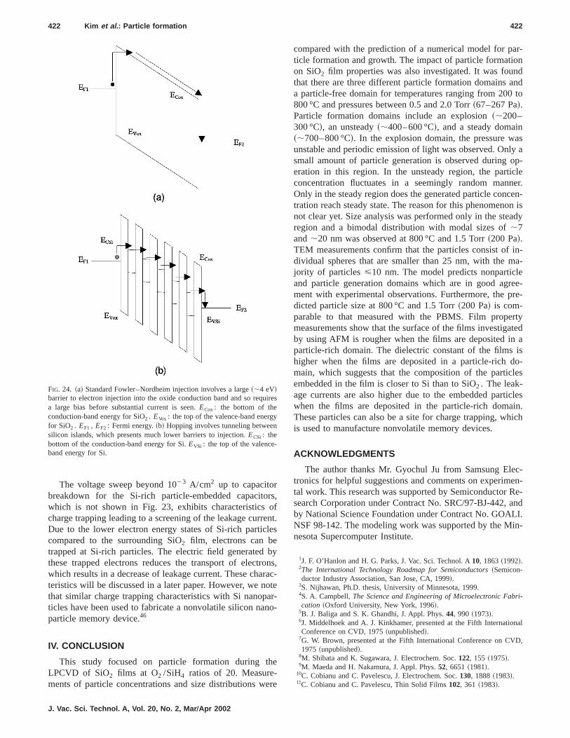
The voltage sweep beyond 1023 A/cm2 up to capacitorbreakdown for the Si-rich particle-embedded capacitowhich is not shown in Fig. 23, exhibits characteristicscharge trapping leading to a screening of the leakage curDue to the lower electron energy states of Si-rich particcompared to the surrounding SiO2 film, electrons can betrapped at Si-rich particles. The electric field generatedthese trapped electrons reduces the transport of electwhich results in a decrease of leakage current. These chateristics will be discussed in a later paper. However, we nthat similar charge trapping characteristics with Si nanopticles have been used to fabricate a nonvolatile silicon naparticle memory device.46
IV. CONCLUSION
This study focused on particle formation during tLPCVD of SiO2 films at O2 /SiH4 ratios of 20. Measure-ments of particle concentrations and size distributions w
FIG. 24. ~a! Standard Fowler–Nordheim injection involves a large~;4 eV!barrier to electron injection into the oxide conduction band and so requa large bias before substantial current is seen.ECox : the bottom of theconduction-band energy for SiO2 . EVox : the top of the valence-band energfor SiO2 . EF1 , EF2 : Fermi energy.~b! Hopping involves tunneling betweensilicon islands, which presents much lower barriers to injection.ECSi : thebottom of the conduction-band energy for Si.EVSi : the top of the valence-band energy for Si.
J. Vac. Sci. Technol. A, Vol. 20, No. 2, Mar ÕApr 2002
s,fnt.s
yns,ac-ter-o-
re
compared with the prediction of a numerical model for pticle formation and growth. The impact of particle formatioon SiO2 film properties was also investigated. It was fouthat there are three different particle formation domains aa particle-free domain for temperatures ranging from 200800 °C and pressures between 0.5 and 2.0 Torr~67–267 Pa!.Particle formation domains include an explosion~;200–300 °C!, an unsteady~;400–600 °C!, and a steady domain~;700–800 °C!. In the explosion domain, the pressure wunstable and periodic emission of light was observed. Onsmall amount of particle generation is observed duringeration in this region. In the unsteady region, the particoncentration fluctuates in a seemingly random manOnly in the steady region does the generated particle contration reach steady state. The reason for this phenomennot clear yet. Size analysis was performed only in the steregion and a bimodal distribution with modal sizes of;7and;20 nm was observed at 800 °C and 1.5 Torr~200 Pa!.TEM measurements confirm that the particles consist ofdividual spheres that are smaller than 25 nm, with the mjority of particles<10 nm. The model predicts nonparticand particle generation domains which are in good agrment with experimental observations. Furthermore, the pdicted particle size at 800 °C and 1.5 Torr~200 Pa! is com-parable to that measured with the PBMS. Film propemeasurements show that the surface of the films investigby using AFM is rougher when the films are deposited inparticle-rich domain. The dielectric constant of the filmshigher when the films are deposited in a particle-rich dmain, which suggests that the composition of the particembedded in the film is closer to Si than to SiO2 . The leak-age currents are also higher due to the embedded partwhen the films are deposited in the particle-rich domaThese particles can also be a site for charge trapping, wis used to manufacture nonvolatile memory devices.
ACKNOWLEDGMENTS
The author thanks Mr. Gyochul Ju from Samsung Eletronics for helpful suggestions and comments on experimtal work. This research was supported by Semiconductorsearch Corporation under Contract No. SRC/97-BJ-442,by National Science Foundation under Contract No. GOANSF 98-142. The modeling work was supported by the Mnesota Supercomputer Institute.
1J. F. O’Hanlon and H. G. Parks, J. Vac. Sci. Technol. A10, 1863~1992!.2The International Technology Roadmap for Semiconductors~Semicon-ductor Industry Association, San Jose, CA, 1999!.
3S. Nijhawan, Ph.D. thesis, University of Minnesota, 1999.4S. A. Campbell,The Science and Engineering of Microelectronic Fabcation ~Oxford University, New York, 1996!.
5B. J. Baliga and S. K. Ghandhi, J. Appl. Phys.44, 990 ~1973!.6J. Middelhoek and A. J. Kinkhamer, presented at the Fifth InternatioConference on CVD, 1975~unpublished!.
7G. W. Brown, presented at the Fifth International Conference on CV1975 ~unpublished!.
8M. Shibata and K. Sugawara, J. Electrochem. Soc.122, 155 ~1975!.9M. Maeda and H. Nakamura, J. Appl. Phys.52, 6651~1981!.
10C. Cobianu and C. Pavelescu, J. Electrochem. Soc.130, 1888~1983!.11C. Cobianu and C. Pavelescu, Thin Solid Films102, 361 ~1983!.
s

em
v,
et
tro
, J
o-
, J.
ci.
ci.
m.
st.
ns
S.
. A
po-hase
. A
.
nol-
423 Kim et al. : Particle formation 423
12P. B. Grabiec and J. Przyluski, Surf. Coat. Technol.25, 307 ~1985!.13P. B. Grabiec and J. Przyluski, Surf. Coat. Technol.25, 315 ~1985!.14P. B. Grabiec and J. Przyluski, Surf. Coat. Technol.27, 219 ~1986!.15H. J. Emeleus and K. Stewart, J. Chem. Soc.1935, 1182.16H. J. Emeleus and K. Stewart, J. Chem. Soc.1936, 677.17K. Strater, RCA Rev.29, 618 ~1968!.18M. L. Barry, presented at the Second International Conference on Ch
cal Vapor Deposition, 1970~unpublished!.19L. L. Vasilyeva, V. N. Drozdov, S. M. Repinsky, and K. K. Svitashe
Thin Solid Films55, 221 ~1978!.20Y. V. Vasiliev, L. L. Vasilieva, V. N. Drozdov, and A. A. Shklyaev, Thin
Solid Films76, 61 ~1981!.21E. A. Taft, J. Electrochem. Soc.126, 1728~1979!.22P. van de Weijer, B. H. Zwerver, and J. L. G. Suijker, Chem. Phys. L
151, 33 ~1988!.23F. B. Ellis, Jr. and J. Houghton, J. Mater. Res.4, 863 ~1989!.24K. Watanabe and H. Komiyama, J. Electrochem. Soc.137, 1222~1990!.25T. Kawahara, A. Yuuki, and Y. Matsui, Jpn. J. Appl. Phys., Part 130, 431
~1991!.26T. Takahashi, K. Hagiwara, Y. Egashira, and H. Komiyama, J. Elec
chem. Soc.143, 1355~1996!.27F. Ojeda, A. Castro-Garcia, C. Gomez-Aleixandre, and J. M. Albella
Mater. Res.13, 2308~1998!.28A. Shintani, K. Suda, M. Suzuki, M. Maki, and K. Takami, J. Electr
chem. Soc.124, 1771~1977!.29A. Shintani, K. Suda, and M. Maki, J. Electrochem. Soc.127, 426~1980!.30M. Liehr and S. A. Cohen, Appl. Phys. Lett.60, 198 ~1992!.31E. Whitby and M. Hoshino, J. Electrochem. Soc.143, 3397~1996!.
JVST A - Vacuum, Surfaces, and Films
i-
t.
-
.
32E. Whitby and M. Hoshino, Rev. Sci. Instrum.66, 3955~1995!.33P. J. Hargis, Jr.et al., Rev. Sci. Instrum.65, 140 ~1994!.34P. J. Ziemann, P. Liu, N. P. Rao, D. B. Kettelson, and P. H. McMurry
Aerosol Sci.26, 745 ~1995!.35P. Liu, P. J. Ziemann, D. B. Kittelson, and P. H. McMurry, Aerosol. S
Technol.22, 293 ~1995!.36P. Liu, P. J. Ziemann, D. B. Kittelson, and P. H. McMurry, Aerosol. S
Technol.22, 314 ~1995!.37P. J. Ziemann, P. Liu, D. B. Kettelson, and P. H. McMurry, J. Phys. Che
99, 5126~1995!.38L. Lieszkovszky and A. R. Filippelli, Vacuum7–9, 2142~1990!.39J. R. Hartman, J. Famil-Ghiriha, M. A. Ring, and H. E. O’Neal, Combu
Flame68, 43 ~1987!.40S. R. Turns,An Introduction to Combustion: Concepts and Applicatio
~McGraw-Hill, New York, 1996!.41P. H. McMurry, S. Nijhawan, N. Rao, P. Ziemann, D. B. Kittelson, and
Campbell, J. Vac. Sci. Technol. A14, 582 ~1996!.42S.-M. Suh, M. R. Zachariah, and S. L. Girshick, J. Vac. Sci. Technol
19, 940 ~2001!.43S.-M. Suh, S. Girshick, and M. Zachariah, Second International Sym
sium on Fundamental Gas-Phase and Surface Chemistry of Vapor-PDeposition, 2001~submitted for proceedings volume!.
44S. Nijhawan, P. H. McMurry, and S. A. Campbell, J. Vac. Sci. Technol18, 2198~2000!.
45D. J. DiMaria, D. W. Dong, C. Falcony, T. N. Theis, J. C. Kirtley, J. CTsang, and S. D. Brorson, J. Appl. Phys.54, 5801~1983!.
46T. Maeda, E. Suzuki, I. Sakata, M. Yamanaka, and K. Ishii, Nanotechogy 10, 127 ~1999!.