output: lv-pecl sg-8503ca / sg-8504ca · • any part of this material may not be reproduced or...
TRANSCRIPT

Actual size
Crystal oscillator
Item Symbol Specifications Conditions / Remarks
Output frequency range f0 50 MHz to 800 MHz -
Supply voltage VCC 2.5 V - 0.125 V to 3.3 V + 0.33 V -
Storage temperature T_stg -55 ºC to +125 ºC Store as bare product after packing
Operating temperature T_use -40 ºC to +85 ºC -
Frequency tolerance *1 f_tol K : ±31.5 × 10
-6 Customized Product (Option)
L : ±50 × 10-6
Current consumption ICC 90 mA Max. OE Active, L_ECL = 50 Ω
Disable current I_dis 40 mA Max. OE Inactive, Output Standby: Hi-Z mode
70 mA Max. OE Inactive, Output Standby: Fix mode
Symmetry SYM 45 % to 55 % At outputs crossing point
Output voltage VOH VCC - 1.025 V Min.
DC characteristics VOL VCC - 1.62 V Max.
Output load condition L_ECL 50 Ω Termination to VCC - 2.0 V
Input voltage VIH 70% VCC Min. SG-8503CA : OE, FSEL
SG-8504CA : OE, FSEL0, FSEL1 VIL 30% VCC Max.
Rise time / Fall time tr/tf 400 ps Max. Between 20% and 80% of (VOH - VOL)
Start-up time t_str 10 ms Max. Time at minimum supply voltage to be 0 s
Setting time for frequency change tSET1 1.5 ms Max.
SG-8503CA : From setting FSEL pin to output new frequency
SG-8504CA : From setting FSEL0 / FSEL1 pin to output new frequency
*1 Frequency tolerance includes initial frequency tolerance, temperature variation, supply voltage change, reflow drift and 10 years aging at +25 ºC.
Product Name SG-8503 CA 156MHz 625MHz A P R L Z (Standard form) Model, Package type, Frequeny-0 (50 ~ 800 MHz), Frequency-1 (50 ~ 800 MHz), Internal crystal frequency, Output enable pin Polarity, Supply voltage/Output format, Frequency tolerance/Operating temperature, Output standby type
Product Name SG-8504 CA 156.2MHz nnnn A P R L Z (Standard form) Model, Package type, Frequeny-0 (50 ~ 800 MHz), Parameter identifier, Internal crystal frequency, Output enable pin Polarity, Supply voltage/Output format, Frequency tolerance/Operating temperature, Output standby type
Internal crystal
frequency
Output enable
pin Polarity
Supply voltage/
Output format
Frequency tolerance/
Operating temperature
Output standby type
A 114.1444 MHz P Active High R 2.5 V ~ 3.3 V/LVPECL K ±31.5 × 10⁻⁶/-40 to +85 °C F Fix (OUT=”L”, OUTN=”H”)
Q Active Low L ±50 × 10-6/-40 to +85 °C Z High-Z
Phase Jitter
Offset Frequency 100.00 MHz 125.00 MHz 156.25 MHz 250.00 MHz 312.50 MHz 500.00 MHz 625.00 MHz
Phase jitter *2 Typ.
12 kHz to 20 MHz 0.31 ps 0.30 ps 0.26 ps 0.26 ps 0.29 ps 0.28 ps 0.29 ps
*2 In order to achieve optimum jitter performance, it is recommended that the capacitor (0.1 μF + 10 μF) between VCC and GND pin should be placed as close to the VCC pin as possible.
Specifications (characteristics)
Dual or Quad Selectable Programmable Crystal Oscillator
Output: LV-PECL
SG-8503CA / SG-8504CA Dual frequency Selectable: SG-8503CA, 7.0 × 5.0 × 1.5 mm (6 pins) Quad frequency Selectable: SG-8504CA, 7.0 × 5.0 × 1.5 mm (8 pins) Frequency range: 50 MHz to 800 MHz Supply voltage: 2.5 V to 3.3 V
Features User-specified two (FSEL) or four (FSEL0, FSEL1) startup frequencies High frequency fundamental tone crystal, Low jitter PLL technology Available field oscillator programmer “SG-Writer ǁ”
Application OTN, BTS, Test Instrument
Product Number (please contact us)
SG-8503CA : X1G005011xxxx00 SG-8504CA : X1G005021xxxx00
V. 11/18
Singel 3 | B-2550 Kontich | Belgium | Tel. +32 (0)3 458 30 33 | [email protected] | www.alcom.be
Rivium 1e straat 52 | 2909 LE Capelle aan den Ijssel | The Netherlands | Tel. +31 (0)10 288 25 00 | [email protected] | www.alcom.nl
Crystal oscillator
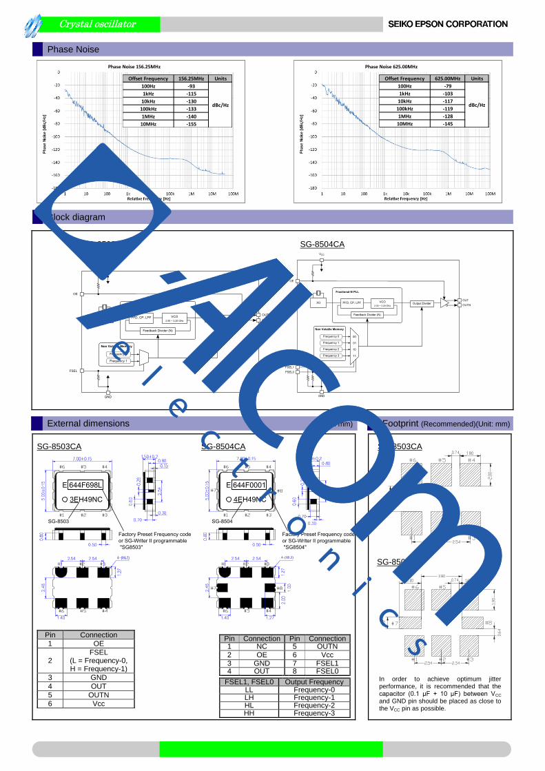
Phase Noise
Block diagram
SG-8503CA SG-8504CA
External dimensions (Unit: mm) Footprint (Recommended)(Unit: mm)
SG-8503CA SG-8504CA
Pin Connection
1 OE
2 FSEL
(L = Frequency-0, H = Frequency-1)
3 GND
4 OUT
5 OUTN
6 Vcc
Pin Connection Pin Connection 1 NC 5 OUTN 2 OE 6 Vcc 3 GND 7 FSEL1 4 OUT 8 FSEL0 FSEL1, FSEL0 Output Frequency
LL Frequency-0 LH Frequency-1 HL Frequency-2 HH Frequency-3
SG-8503CA
SG-8504CA
Offset Frequency 156.25MHz Units
100Hz -93
1kHz -115
10kHz -130
100kHz -133
1MHz -140
10MHz -155
dBc/Hz
Offset Frequency 625.00MHz Units
100Hz -79
1kHz -103
10kHz -117
100kHz -119
1MHz -128
10MHz -145
dBc/Hz
In order to achieve optimum jitter performance, it is recommended that the capacitor (0.1 μF + 10 μF) between VCC and GND pin should be placed as close to the VCC pin as possible.

Crystal oscillator
Simulation Model
IBIS model is available. Please contact us.
ESD Rating
Human Body Model (HBM) 2000 V
Machine Model (MM) 200 V
Device Material & Environmental Information
Model Package Dimensions # of
Pins
Reference
Weight
(Typ.)
Terminal
Material
Terminal
Plating
Complies
With EU
RoHS
Pb
Free
MSL
Rating
Peak
Temp
(Max)
SG-8503CA 7.0 x 5.0 x 1.5 mm
6 167 mg W Au Yes Yes 1 260 °C
SG-8504CA 8 168 mg
●Pb free.
●Complies with EU RoHS directive.
*About the products without the Pb-free mark.
Contains Pb in products exempted by EU RoHS directive.
(Contains Pb in sealing glass, high melting temperature type solder or other.)

Crystal oscillator
Device Marking
Model Factory Programmed Part Marking Field Programmable Part Marking (Blank Samples)
SG-8503CA
SG-8504CA
Standard Packing Specification
SMD products are packed in the shipping carton as below table in accordance with taping standards EIA-481 and IEC-60286
Standard Packing Quantity and Dimension (Unit: mm)
Model Quantity
(pcs/Reel)
Reel dimension Career Tape dimension Direction of feed
(L=left direction) a b W A B C D
SG-8503CA
SG-8504CA 1000 Φ180 Φ60 17 8 9.25 16 2.1 L
b
a
2.0 or 1.2
1.0R
Φ21.0
Φ13.0
1.0R
W
2.0
φ1.5 4.0
B
C
A D
Top tape
Carrier Tape
Direction of feed
EP
SO
N
EP
SO
N

PROMOTION OF ENVIRONMENTAL MANAGEMENT SYSTEM CONFORMING TO INTERNATIONAL STANDARDS
At Seiko Epson, all environmental initiatives operate under the Plan-Do-Check-Action (PDCA) cycle designed to achieve continuous improvements. The environmental management system (EMS) operates under the ISO 14001 environmental management standard.
All of our major manufacturing and non-manufacturing sites, in Japan and overseas, completed the acquisition of ISO 14001 certification.
WORKING FOR HIGH QUALITY In order provide high quality and reliable products and services
than meet customer needs, Seiko Epson made early efforts towards obtaining ISO9000 series
certification and has acquired ISO9001 for all business establishments in Japan and abroad. We have also acquired ISO/TS 16949 certification that is requested strongly by major automotive manufacturers as standard.
►Explanation of the mark that are using it for the catalog
►Pb free.
►Complies with EU RoHS directive. *About the products without the Pb-free mark. Contains Pb in products exempted by EU RoHS directive. (Contains Pb in sealing glass, high melting temperature type solder or other.)
►Designed for automotive applications such as Car Multimedia, Body Electronics, Remote Keyless Entry etc.
►Designed for automotive applications related to driving safety (Engine Control Unit, Air Bag, ESC etc ).
Seiko Epson Corporation
Notice • This material is subject to change without notice. • Any part of this material may not be reproduced or duplicated in any form or any means without the written permission of Seiko Epson. • The information about applied data, circuitry, software, usage, etc. written in this material is intended for reference only. Seiko Epson
does not assume any liability for the occurrence of customer damage or infringing on any patent or copyright of a third party. This material does not authorize the licensing for any patent or intellectual copyrights.
• When exporting the products or technology described in this material, you should comply with the applicable export control laws and regulations and follow the procedures required by such laws and regulations.
• You are requested not to use the products (and any technical information furnished, if any) for the development and/or manufacture of weapon of mass destruction or for other military purposes. You are also requested that you would not make the products available to any third party who may use the products for such prohibited purposes.
• These products are intended for general use in electronic equipment. When using them in specific applications that require extremely high reliability, such as the applications stated below, you must obtain permission from Seiko Epson in advance.
/ Space equipment (artificial satellites, rockets, etc.) / Transportation vehicles and related (automobiles, aircraft, trains, vessels, etc.) / Medical instruments to sustain life / Submarine transmitters / Power stations and related / Fire work equipment and security equipment / traffic control equipment / and others requiring equivalent reliability.
• All brands or product names mentioned herein are trademarks and/or registered trademarks of their respective.
ISO 14000 is an international standard for environmental management that was established by the International Standards Organization in 1996 against the background of growing concern regarding global warming, destruction of the ozone layer, and global deforestation.
ISO/TS16949 is the international standard that added the sector-specific supplemental requirements for automotive industry based on ISO9001.
Singel 3 | B-2550 Kontich | Belgium | Tel. +32 (0)3 458 30 33 | [email protected] | www.alcom.be
Rivium 1e straat 52 | 2909 LE Capelle aan den Ijssel | The Netherlands | Tel. +31 (0)10 288 25 00 | [email protected] | www.alcom.nl