opti510r: photonics - wp.optics.arizona.edu · the most obvious method of measuring ber is to brute...
TRANSCRIPT

OPTI510R: Photonics
Khanh Kieu
College of Optical Sciences,
University of Arizona
Meinel building R.626

Announcements
Homework #6 is due on Wednesday, April 25
Final exam May 2, room 307

Introduction to Optical Network
Modulation formats
Signal multiplexing
• Time
• Code
• Wavelength
System performance
• Bit Error Rate
• Optical signal to noise ratio
• Eye diagram
Network architecture, limitation
CIAN
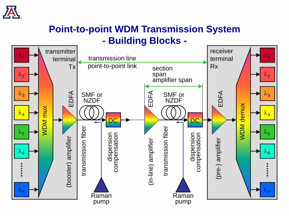
l1
l2
l3
l4
l5
l6
ln
WD
M m
ux
l1
l2
l3
l4
l5
l6
ln
WD
M d
em
ux
(booste
r) a
mplif
ier
transmitter
terminal
Tx
receiver
terminal
Rx
(pre
-) a
mplif
ier
(in
-lin
e)
am
plif
ier
ED
FA
ED
FA
ED
FA
transm
issio
n fib
er
transm
issio
n fib
er
dis
pers
ion
co
mp
en
sa
tio
n
dis
pers
ion
com
pen
sation
DC DC
Ramanpump
Ramanpump
sectionspanamplifier span
transmission line
point-to-point link
SMF orNZDF
SMF orNZDF
Point-to-point WDM Transmission System
- Building Blocks -
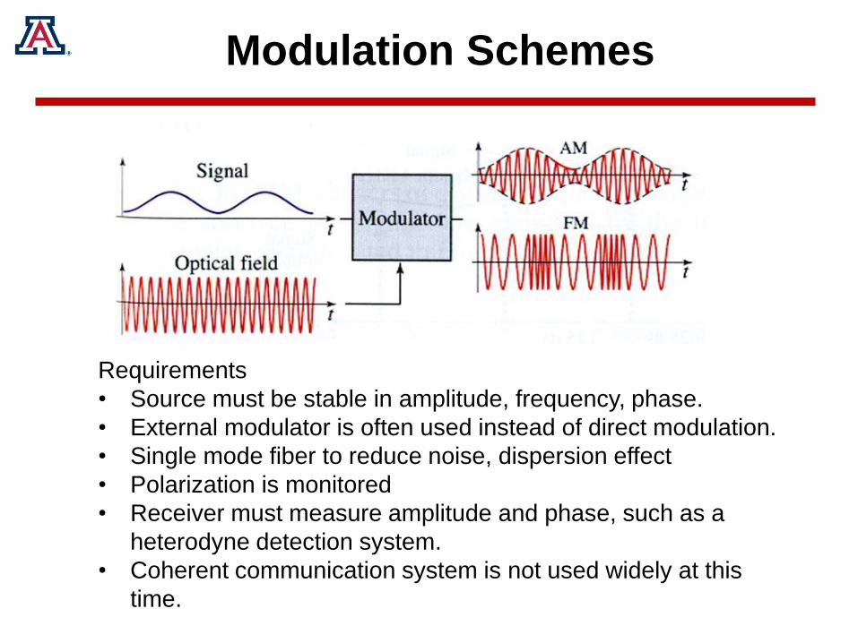
Modulation Schemes
Requirements
• Source must be stable in amplitude, frequency, phase.
• External modulator is often used instead of direct modulation.
• Single mode fiber to reduce noise, dispersion effect
• Polarization is monitored
• Receiver must measure amplitude and phase, such as a
heterodyne detection system.
• Coherent communication system is not used widely at this
time.
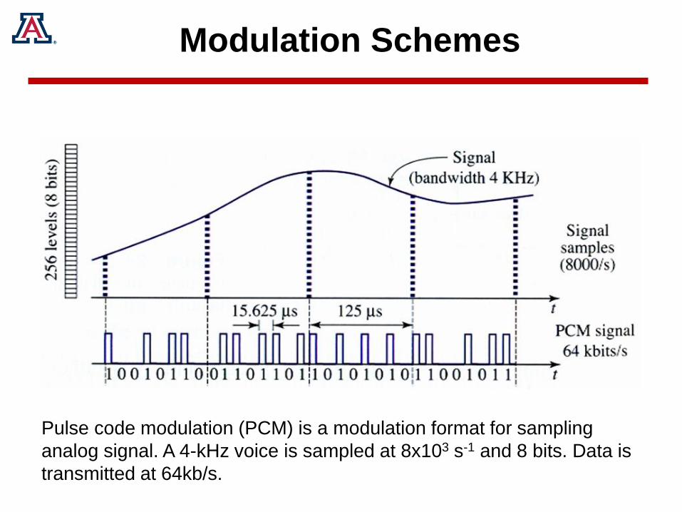
Modulation Schemes
Pulse code modulation (PCM) is a modulation format for sampling
analog signal. A 4-kHz voice is sampled at 8x10³ s-1 and 8 bits. Data is
transmitted at 64kb/s.

Modulation Formats
(a)On-Off keying (OOK) intensity modulation
(b)Frequency shift keying (FSK) and phase shift keying (PSK)
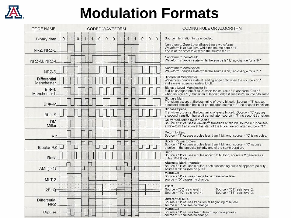
Modulation Formats
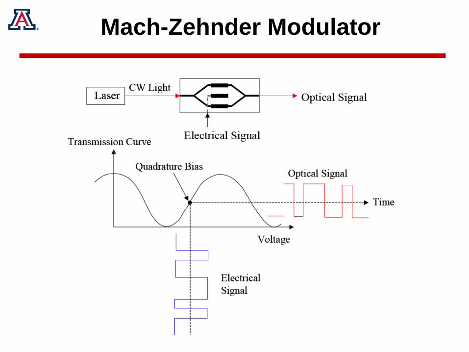
Mach-Zehnder Modulator
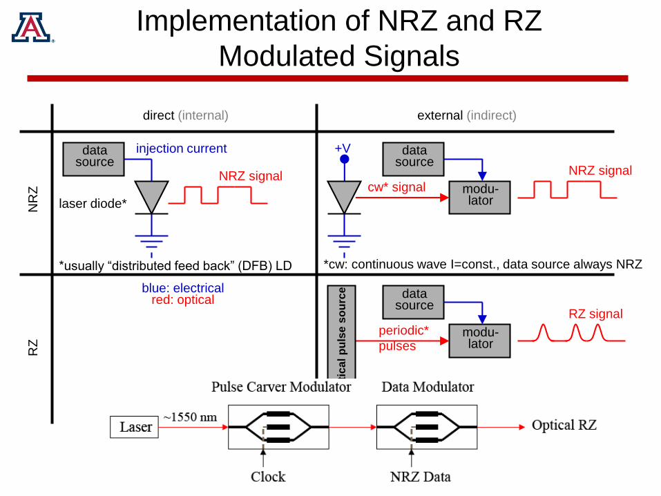
Implementation of NRZ and RZ
Modulated Signals
direct (internal) external (indirect)
NR
ZR
Z
datasource
injection current
NRZ signal
laser diode*
*usually “distributed feed back” (DFB) LD
+V datasource
modu-lator
cw* signal
NRZ signal
*cw: continuous wave I=const., data source always NRZ
datasource
modu-lator
periodic*
pulses
RZ signal
*pulse repetition rate frep = B
op
tic
al
pu
lse
so
urc
eblue: electricalred: optical

Prof. Norwood
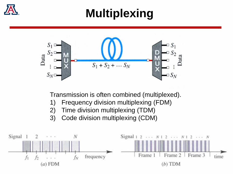
Multiplexing
Transmission is often combined (multiplexed).
1) Frequency division multiplexing (FDM)
2) Time division multiplexing (TDM)
3) Code division multiplexing (CDM)

Multiplexing
Example of TDM
T system: A set of 24 4-kb/s signals are combined to a T1 at 1.544 Mb/s signal.
A set of T1 is combined to T2 at 6.312 Mb/s.

Multiplexing
Code division multiplexing
1) Each sender has a code, corresponding
to one vector, v, from a group of
orthogonal vectors
2) Associate data 0 with –v and 1 with +v
3) Data from all senders are combined and
transmitted
4) Data are decoded for each sender using
unique vector at receiving end
Example of 4 orthogonal
digital signals.
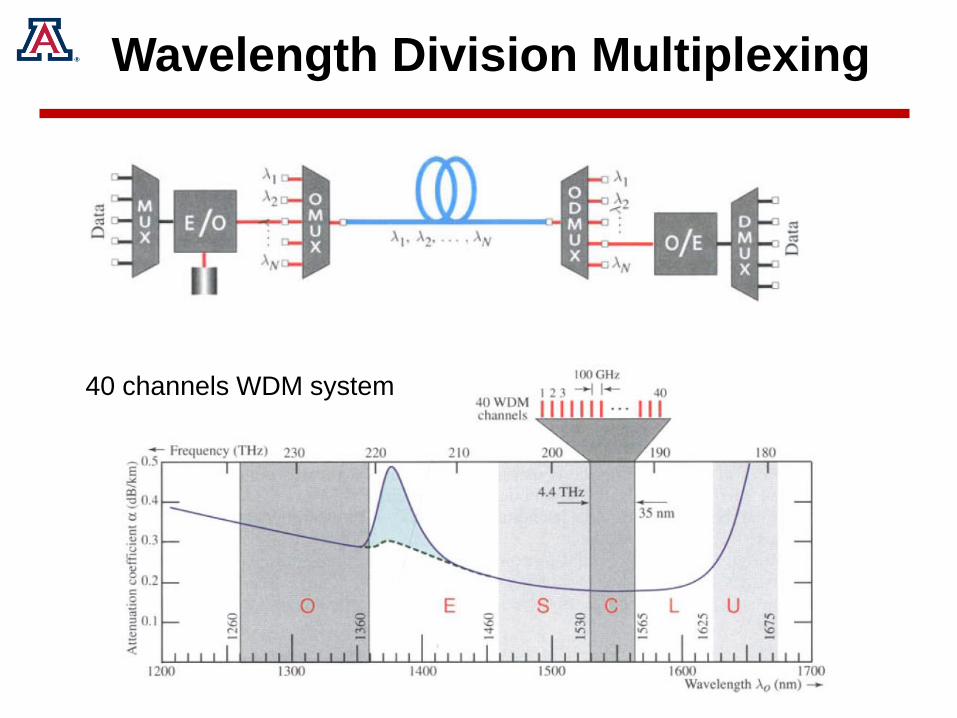
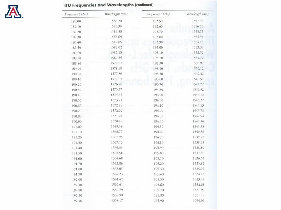
Wavelength Division Multiplexing
40 channels WDM system
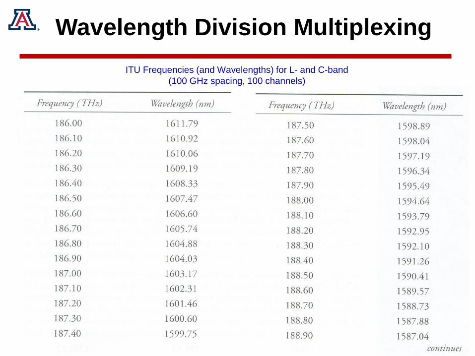
ITU Frequencies (and Wavelengths) for L- and C-band
(100 GHz spacing, 100 channels)
Wavelength Division Multiplexing

System Performance
Important parameters of a digital communication system
• Bit error rate: BER• Optical signal to noise: OSNR• Q factor
All parameters are monitored regularly to track the health of the network
Parameters are related to each other
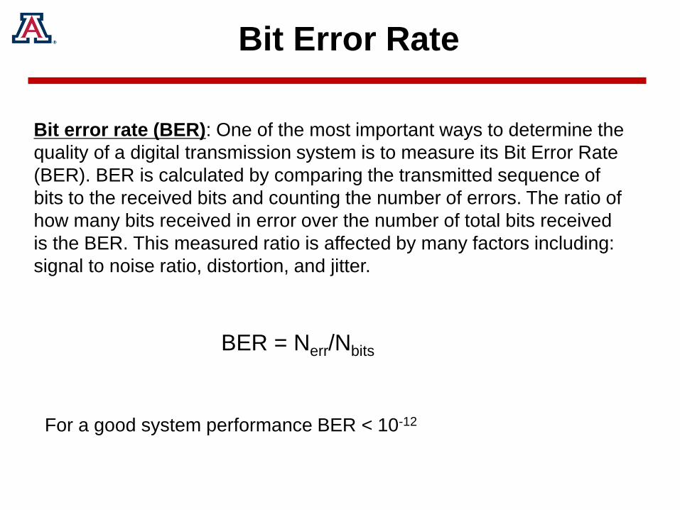
Bit Error Rate
Bit error rate (BER): One of the most important ways to determine the
quality of a digital transmission system is to measure its Bit Error Rate
(BER). BER is calculated by comparing the transmitted sequence of
bits to the received bits and counting the number of errors. The ratio of
how many bits received in error over the number of total bits received
is the BER. This measured ratio is affected by many factors including:
signal to noise ratio, distortion, and jitter.
BER = Nerr/Nbits
For a good system performance BER < 10-12

Bit Error Rate
The most obvious method of measuring BER is to brute force send bits through the system
and calculate the BER. Since this is a statistical process, the measured BER only
approaches the actual BER as the number of bits tested approaches infinity.
Fortunately, in most cases we need only to test that the BER is less than a predefined
threshold. The number of bits required to accomplish this will only depend on the required
confidence level and BER threshold. The confidence level is the percentage of tests that
the system’s true BER is less than the specified BER. Since we cannot measure an infinite
number of bits and it is impossible to predict with certainty when errors will occur,
the confidence level will never reach 100%.
To calculate the confidence level (CL), we use the equation:
This equation can be rearranged to calculate the number of bits required for a
given BER and confidence level (CL):

Bit Error Rate
In order to determine the test time required, the number of bits to be tested is
simply divided by the data rate
STM-256/OC-
768
39.81312
GHz
STM-264/OC-
192
9.95328 GHz
STM-16/OC-
48
2.48832 GHz
STM-4/OC-12
622.08 MHz
STM-1/OC-3
155.52 MHz
10-16
~ 8.7 days ~ 35 days ~ 139 days ~ 2 yrs ~ 8.4 yrs
10-15
~ 21 hrs ~ 3.5 days ~ 30 days ~ 42 days ~ 224 days
10-14
~ 2.1 hrs ~ 8.4 hrs ~ 1.4 days ~ 5.6 days ~ 22.4 days
10-13
~ 12.5 mins ~ 50 mins ~ 3.3 hrs ~ 13 hrs ~ 2.2 days
10-12
~ 1.3 mins ~ 5 mins ~ 20 mins ~ 80 mins ~ 5.35 hrs
10-11
~ 7.5 secs ~ 30 secs ~ 2 mins ~ 8 mins ~ 32 mins
A table of test times at 95% confidence level is given for standard data rates and bit error ratios
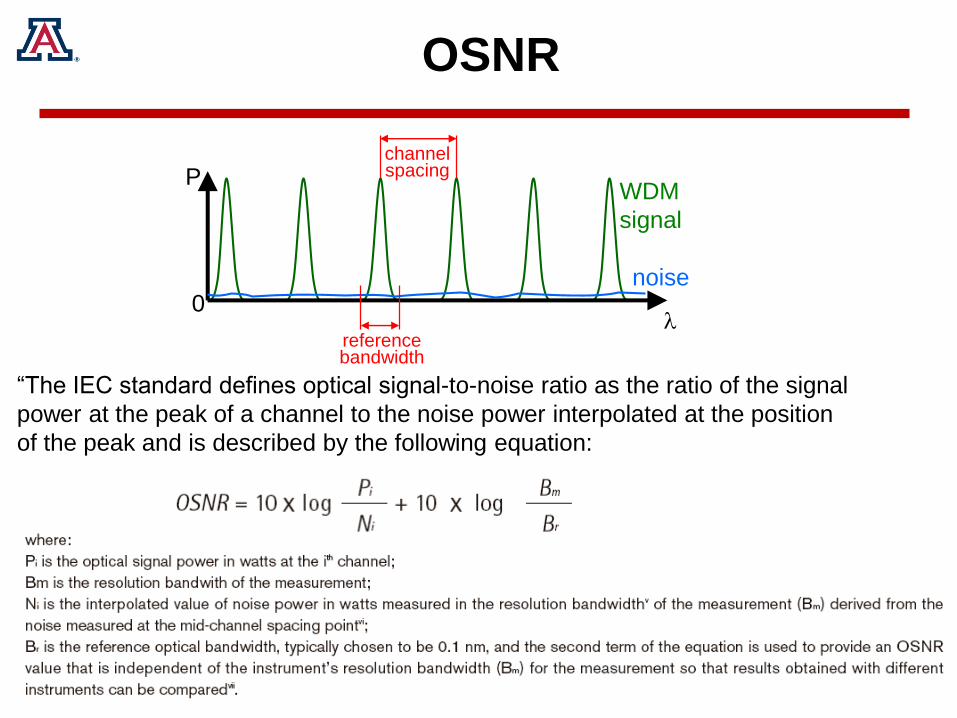
OSNR
P
0
channelspacing
l
noise
WDM
signal
referencebandwidth
“The IEC standard defines optical signal-to-noise ratio as the ratio of the signal
power at the peak of a channel to the noise power interpolated at the position
of the peak and is described by the following equation:

OSNR
Noise power is usually interpolated at the peak
OSNR can be correlated to the BER. According to IEC 61280-2-7 draft document,
)2
exp(2
1 2
SNR
tdtBER

Bit Error Testing-Eye diagram
An eye diagram is a common indicator of the quality of signals in high-speed digital transmissions.
An oscilloscope generates an eye diagram by overlaying sweeps of different segments of a
long data stream driven by a master clock.
In practical terms this may be achieved by displaying the data
waveform on a sampling oscilloscope triggered from the system clock.

Q-factor
The performance of digital fiber-optic transmission systems can be specified
using the Q-factor. The Q-factor is the electrical signal-to-noise ratio (SNR) at
the input of the decision circuit in the receiver terminal Rx.
For the purpose of calculation, the signal level is interpreted as the difference
in the mean values 0 and 1, and the noise level is the sum of the standard
deviations 0 and 1 at the sampling time:
Q-factor
Bit Error Testing-Eye diagram
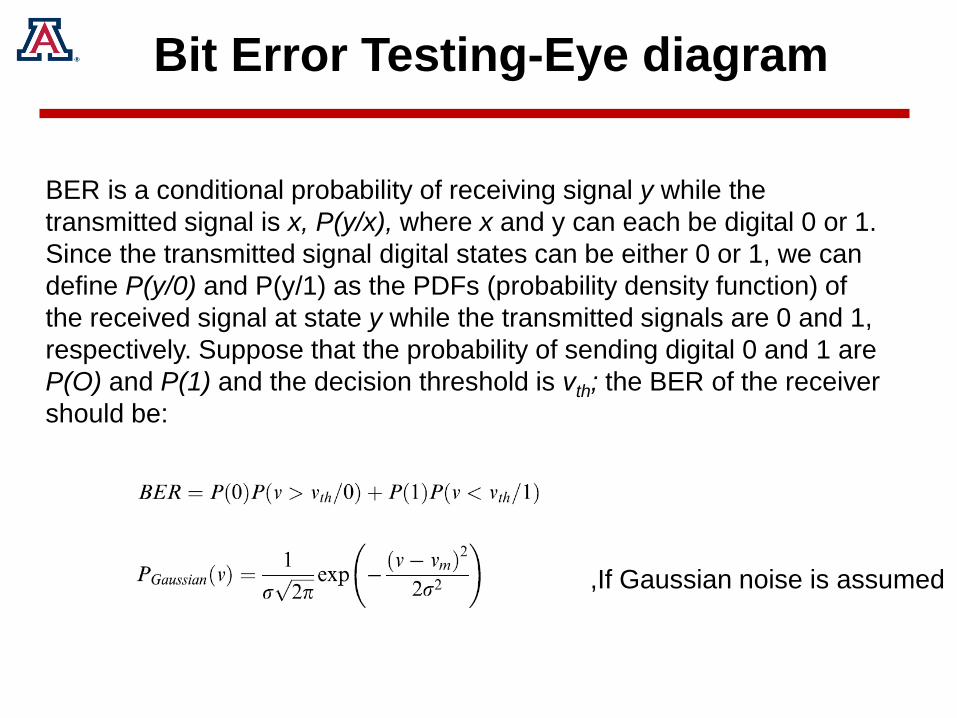
BER is a conditional probability of receiving signal y while the
transmitted signal is x, P(y/x), where x and y can each be digital 0 or 1.
Since the transmitted signal digital states can be either 0 or 1, we can
define P(y/0) and P(y/1) as the PDFs (probability density function) of
the received signal at state y while the transmitted signals are 0 and 1,
respectively. Suppose that the probability of sending digital 0 and 1 are
P(O) and P(1) and the decision threshold is vth; the BER of the receiver
should be:
,If Gaussian noise is assumed

Bit Error Testing-Eye diagram
The probability for the receiver to declare 1 while the transmitter actually sends a 0 is:
,Where ,Q-value or quality factor
Similarly, the probability for the receiver to declare 0 while the transmitter actually sends a 1 is:
,P(0) = P (1) = 0.5
is assumed

Bit Error Testing-Eye diagram
A widely used mathematical function, the error function, is defined as:
And the complementary error function is defined as:
Bit Error Testing-Eye diagram
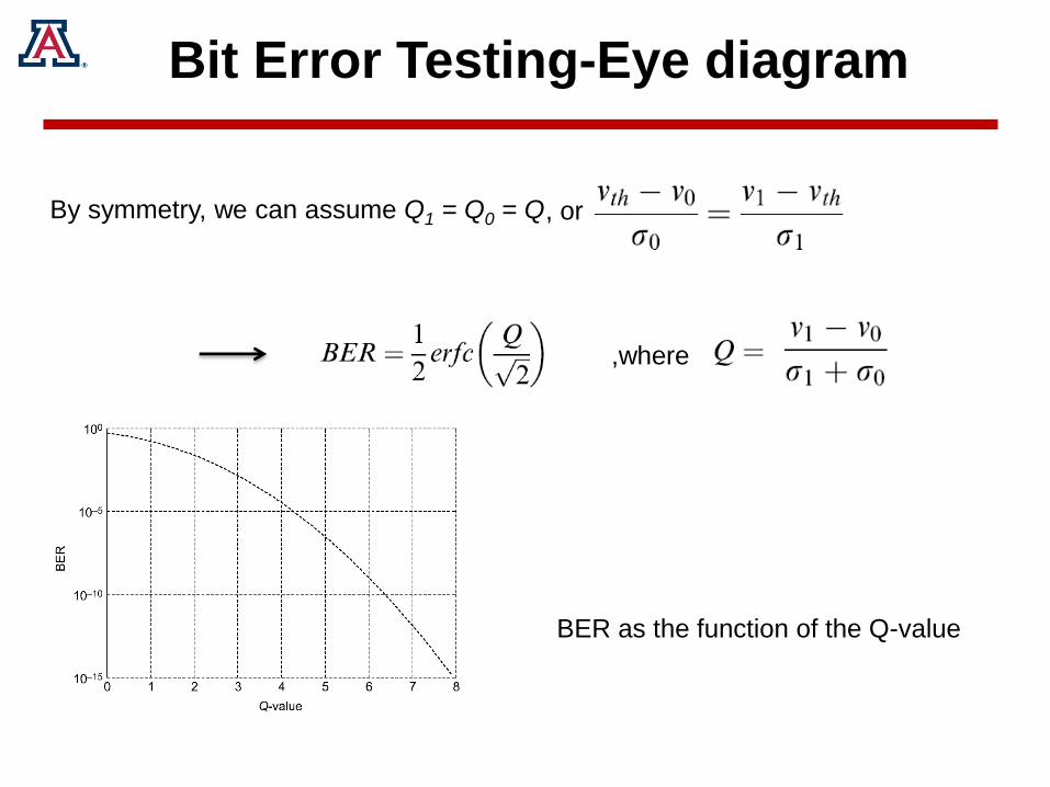
By symmetry, we can assume Q1 = Q0 = Q, or
,where
BER as the function of the Q-value

Network Topology
Topology
Star
Ring
Meshed
Point-to-point
200 m
2 km
100 km
2,000 km
10,000 km

Network Topology
• - From “In-house” to “Submarine” -
In-house
Plastic optical fiber POF
10/100 Mbit/s Ethernet
Different
requirements:
low-cost
flexible
manageable
reliable
Campus / LANMultimode fiber100 Mb/s / 1 Gb/sEthernet
City / MAN
Singlemode fiber
2.5 Gbit/s SONET
National backbone / WAN
Singlemode fiber
N10 Gbit/s SONET / OTN
Global / submarine
Singlemode fiber
N10 Gbit/s
SONET / OTN

Network Technologies
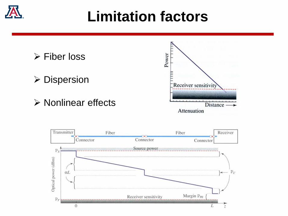
Limitation factors
Fiber loss
Dispersion
Nonlinear effects

Limitation factors
1. At higher bit rate, transmission is more sensitive to attenuation. For a
fixed power, higher bit rate means fewer photons per bit and more photon
noise.
2. At higher bit rate, pulse is shorter and spectrum is wider. Dispersion, and
nonlinear effects such as intersymbol interference (ISI) become important.
3. At fixed number of photon per bit, higher bit rate means greater optical
power.
ISI: Intersymbol interference
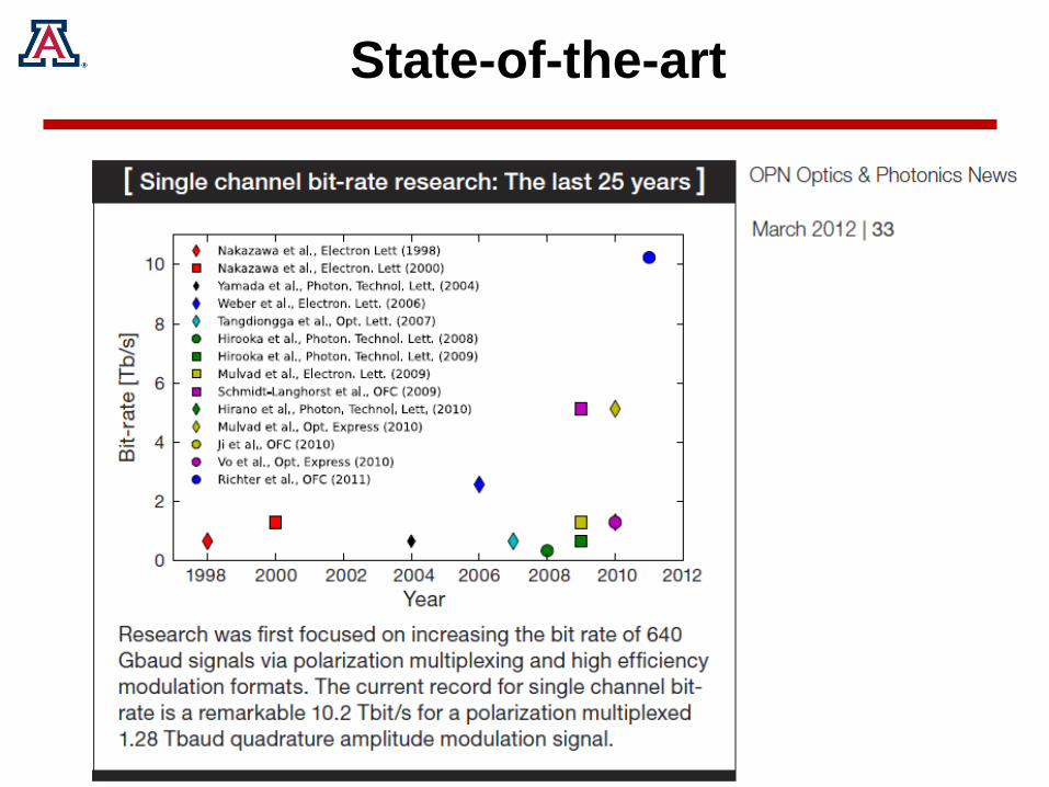
State-of-the-art

36
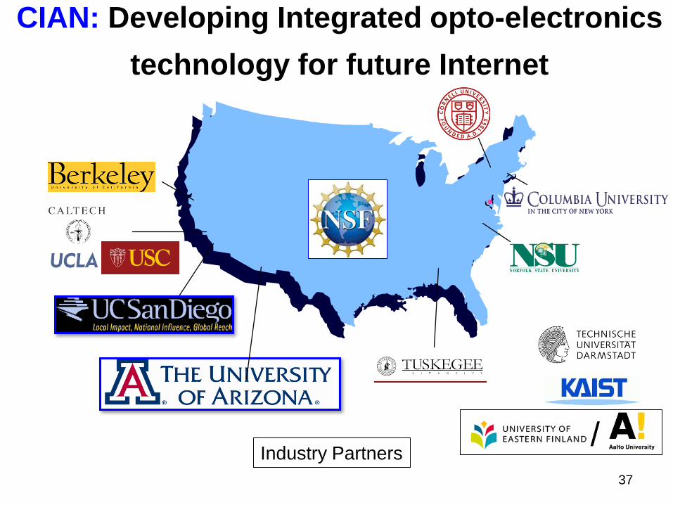
CIAN: Developing Integrated opto-electronics
technology for future Internet
Prof. Nasser Peyghambarian
Center Director, Faculty
University of Arizona
520-621-4649
http://www.cian-erc.org/people.cfm?type=faculty
37
CIAN: Developing Integrated opto-electronics
technology for future Internet
/Industry Partners
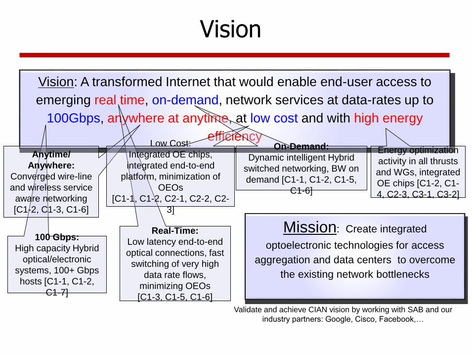
Vision
Vision: A transformed Internet that would enable end-user access to
emerging real time, on-demand, network services at data-rates up to
100Gbps, anywhere at anytime, at low cost and with high energy
efficiency
Real-Time:
Low latency end-to-end
optical connections, fast
switching of very high
data rate flows,
minimizing OEOs
[C1-3, C1-5, C1-6]
100 Gbps:
High capacity Hybrid
optical/electronic
systems, 100+ Gbps
hosts [C1-1, C1-2,
C1-7]
Anytime/
Anywhere:
Converged wire-line
and wireless service
aware networking
[C1-2, C1-3, C1-6]
On-Demand:
Dynamic intelligent Hybrid
switched networking, BW on
demand [C1-1, C1-2, C1-5,
C1-6]
Low Cost:
Integrated OE chips,
integrated end-to-end
platform, minimization of
OEOs
[C1-1, C1-2, C2-1, C2-2, C2-
3]
Energy optimization
activity in all thrusts
and WGs, integrated
OE chips [C1-2, C1-
4, C2-3, C3-1, C3-2]
Validate and achieve CIAN vision by working with SAB and our
industry partners: Google, Cisco, Facebook,…
Mission: Create integrated
optoelectronic technologies for access
aggregation and data centers to overcome
the existing network bottlenecks

39
Strategic Research Plan

Thrust 2:SubsystemIntegration& SiliconNanophotonics
Thrust 1:OpticalCommunicationSystems& Networking
Re
sear
chP
roje
cts
Working Group II:Intelligent Access
AggregationNetworks
Use Cases:Telepresence, 3D holographic
Video
Working Group I:Scalable
& Energy EfficientData Centers
Thrust 3:Device Physics& Fundamentals
Re
sear
chP
roje
cts
Re
sear
chP
roje
cts
Packaging & TestUA
Optical Aggregation Testbed (TOAN)
UA
Data CenterTestbed
UCSD
Use Cases:Efficient Data centersYou Tube, Facebook
Chip scale Testing
UA and UCSD
DataIntrospection
USC
Cross-layerOptimization
Columbia
Network IntegrationUCSD
Optical DeviceCharacterization
UA
Working Groups (WG) integrate research across 3 thrusts

Testbeds
• MORDIA (24 servers)
• Chip-scale testing and insertion from Sandia, Columbia/Cornell
• Wavelength translation through parametric processing
Servers
Opt. Amps
Hardware forstations
OSA
Front of Rack Back of Rack
Opt. Amps
PatchPanel
Network NodesCIAN Insertion Stations
Aggregation NetworkData Center Network