ncv70522dq - micro-stepping motor driver ssop36
TRANSCRIPT

© Semiconductor Components Industries, LLC, 2015
February, 2015 − Rev. 21 Publication Order Number:
NCV70522DQ/D
NCV70522DQ
Micro-Stepping Motor DriverIntroduction
The NCV70522DQ is a micro−stepping stepper motor driver forbipolar stepper motors. The chip is connected through I/O pins and aSPI interface with an external microcontroller. The NCV70522DQfeatures an internal current−translation table: it takes the nextmicro−step depending on the clock signal on the stepping input pin(NXT) and the status of the direction register or input pin (DIR). Areliable current control is achieved using an integrated proprietaryPWM algorithm.
The NCV70522DQ includes a so−called “Speed and Load Angle”(SLA) output, allowing the creation of stall detection algorithms andcontrol loops to adjust torque and speed based on the motor’s backelectromotive force (BEMF).
The NCV70522DQ is implemented in I2T100 technology, enablingboth high voltage analog circuitry and digital functionality on thesame chip. The device is fully compatible with automotive voltage andtemperature requirements and suited to general purpose stepper motorapplications in the automotive, industrial, medical and marinedomains.
Features• Dual H−Bridge for 2 Phase Stepper Motors
• Programmable Peak−Current up to 1.2 A Continuous (1.5 A ShortTime), Using a 5−Bit Current DAC
• On−Chip Current Translator
• SPI Interface
• Speed and Load−Angle Output
• 7 Step Modes from Full−Step up to 32 Micro−Steps
• Fully Integrated Current−Sense
• PWM Current Control with Automatic Selection of Fast and SlowDecay
• Low EMC PWM with Selectable Voltage Slopes
• Active Fly−back Diodes
• Full Output Protection and Diagnosis
• Thermal Warning and Shutdown
• Digital IO’s Compatible with 5 V and 3.3 V Microcontrollers
• Integrated 5 V Voltage Regulator to Supply an ExternalMicrocontroller
• Integrated Reset Function to Reset External Microcontroller
• Integrated Watchdog Function
• NCV Prefix for Automotive and Other Applications Requiring Siteand Control Changes
• These are Pb−Free Devices*
*For additional information on our Pb−Free strategy and soldering details, pleasedownload the ON Semiconductor Soldering and Mounting TechniquesReference Manual, SOLDERRM/D.
www.onsemi.com
See detailed ordering and shipping information in the packagedimensions section on page 27 of this data sheet.
ORDERING INFORMATION
SSOP36 EPDQ SUFFIX
CASE 940AB
MARKING DIAGRAM
NCV70522−4AWLYYWWG
NCV70522 = Specific Device CodeA = Assembly LocationWL = Wafer LotYY = YearWW = Work WeekG = Pb−Free Package

NCV70522DQ
www.onsemi.com2
Figure 1. Block Diagram NCV70522DQTST0 GND
MOTXN
MOTYP
MOTYN
CLK
DI
DO
NXT
DIR
SLA
CLR
Timebase Charge Pump
Logic &Registers Load
Angle
Temp.Sense
Band−gap
OTP
POR
SPI
I−sense
EMC
I−sense
EMC
PW
M
NCV70522DQ
PW
M
TR
AN
SLA
TO
R
CPN CPP VCP VBB
CS
ERR
MOTXP
POR/WD
Vreg
VDD
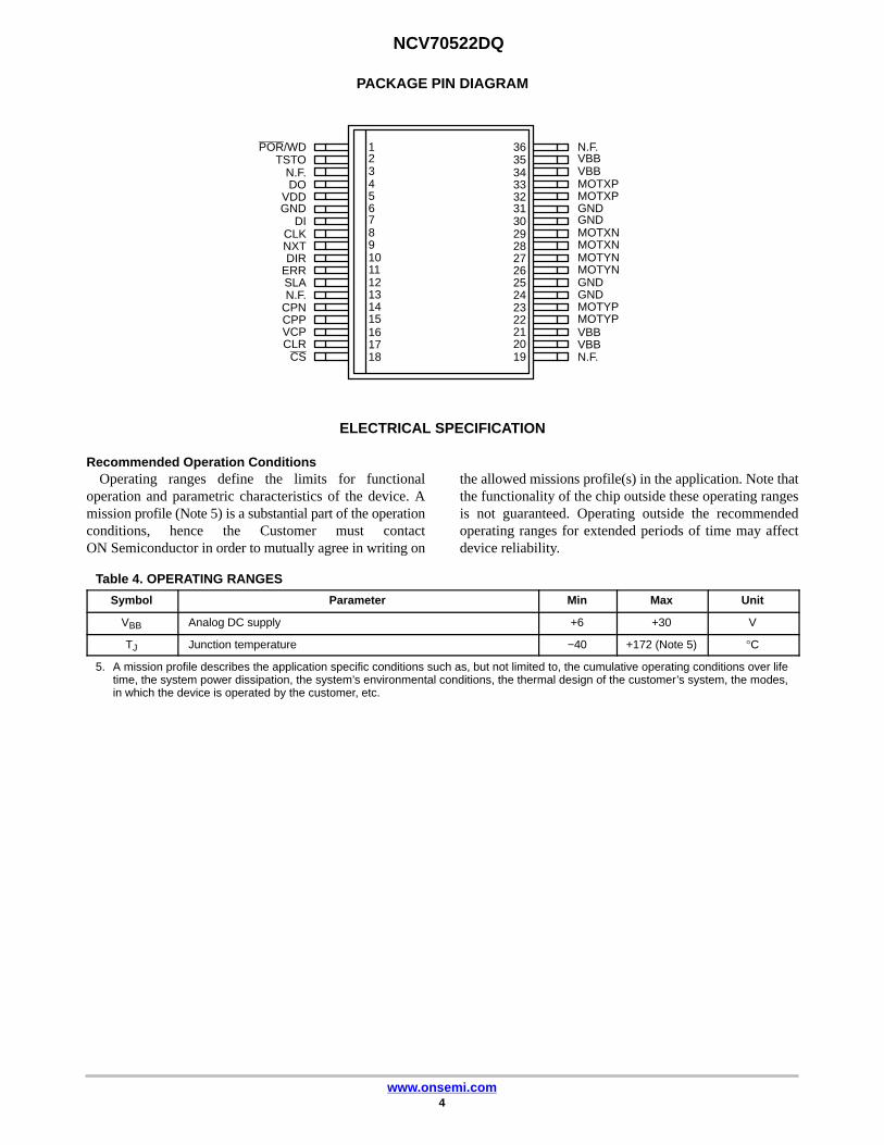
Table 1. PIN DESCRIPTION
Name Pin Description Type Equivalent Schematic
POR/WD 1 Power On Reset and Watchdog Reset Output Digital Output Type 4
TST0 2 Test Pin Input (to be Tied to Ground in Normal Operation) Digital Input
/ 3, 19, 36 No Function (to be Tied to Ground)
DO 4 SPI Data Output (Open Drain) Digital Output Type 4
VDD 5 Logic Supply Output (Needs External Decoupling Capacitor) Supply Type 3
GND 6 Ground Supply
DI 7 SPI Data In Digital Input Type 2
CLK 8 SPI Clock Input Digital Input Type 2
NXT 9 Next Micro−Step Input Digital Input Type 2
DIR 10 Direction Input Digital Input Type 2
ERR 11 Error Output (Open Drain) Digital Output Type 4
SLA 12 Speed Load Angle Output Analog Output Type 5
/ 13 No Function (to be Tied to Ground)
CPN 14 Negative Connection of Charge Pump Capacitor High Voltage
CPP 15 Positive Connection of Charge Pump Capacitor High Voltage
VCP 16 Charge−Pump Filter−Capacitor High Voltage
CLR 17 “Clear” = Chip Reset Input Digital Input Type 1
CS 18 SPI Chip Select Input Digital Input Type 2
VBB 20, 21 High Voltage Supply Input Supply Type 3
MOTYP 22, 23 Positive End of Phase Y Coil Output Driver Output
GND 24, 25 Ground Supply
MOTYN 26, 27 Negative End of Phase Y Coil Output Driver Output
MOTXN 28, 29 Negative End of Phase X Coil Output Driver Output
GND 30, 31 Ground Supply
MOTXP 32, 33 Positive End of Phase X Coil Output Driver Output
VBB 34, 35 High Voltage Supply Input Supply Type 3

NCV70522DQ
www.onsemi.com3
Table 2. ABSOLUTE MAXIMUM RATINGS
Symbol Parameter Min Max Unit
VBB Analog DC Supply Voltage (Note 1) −0.3 +40 V
TST Storage Temperature −55 +160 °C
TJ Junction Temperature (Note 2) −50 +175 °C
VESD Electrostatic Discharges on Component Level, All Pins (Note 3) −2 +2 kV
VESD Electrostatic Discharges on Component Level, HiV Pins (Note 4) −8 +8 kV
Stresses exceeding those listed in the Maximum Ratings table may damage the device. If any of these limits are exceeded, device functionalityshould not be assumed, damage may occur and reliability may be affected.1. For limited time < 0.5 s2. Circuit functionality not guaranteed.3. Human Body Model (100 pF via 1.5 k�, according to JEDEC EIA−JESD22−A114−B)4. HiV = High Voltage Pins MOTxx, VBB, GND; Human Body Model (100 pF via 1.5 k�, according to JEDEC EIA−JESD22−A114−B)
Table 3. THERMAL RESISTANCE
Package
Thermal Resistance
UnitJunction−to−Exposed Pad
SSOP36−EP 3.5 K/W
EQUIVALENT SCHEMATICS
The following figure gives the equivalent schematics of the user relevant inputs and outputs. The diagrams are simplifiedrepresentations of the circuits used.
Figure 2. In− and Output Equivalent Diagrams
IN
IN
VDD
OUT
SLA
4k
4k
VBB
VDD VBB
Rout
TYPE 1: CLR Input
TYPE 2: CLK, DI, CS, NXT, DIR Inputs
TYPE 4: DO and ERR OpenDrain Outputs
TYPE 5: SLA Analog Output
TYPE 3: VDD and VBB Power Supply
Rpd
NCV70522DQ
www.onsemi.com4
PACKAGE PIN DIAGRAM
POR/WDTSTO
DOVDDGND
DICLKNXTDIR
ERRSLA
CPNCPPVCPCLR
CS
VBBVBBMOTXPMOTXPGNDGNDMOTXNMOTXNMOTYNMOTYNGNDGNDMOTYPMOTYPVBBVBBN.F.
N.F.
N.F.
N.F.23456789101112131415161718
1 3635
333231302928272625
2322212019
24
34
ELECTRICAL SPECIFICATION
Recommended Operation ConditionsOperating ranges define the limits for functional
operation and parametric characteristics of the device. Amission profile (Note 5) is a substantial part of the operationconditions, hence the Customer must contactON Semiconductor in order to mutually agree in writing on
the allowed missions profile(s) in the application. Note thatthe functionality of the chip outside these operating rangesis not guaranteed. Operating outside the recommendedoperating ranges for extended periods of time may affectdevice reliability.
Table 4. OPERATING RANGES
Symbol Parameter Min Max Unit
VBB Analog DC supply +6 +30 V
TJ Junction temperature −40 +172 (Note 5) °C
5. A mission profile describes the application specific conditions such as, but not limited to, the cumulative operating conditions over lifetime, the system power dissipation, the system’s environmental conditions, the thermal design of the customer’s system, the modes,in which the device is operated by the customer, etc.

NCV70522DQ
www.onsemi.com5
Table 5. DC PARAMETERS(The DC Parameters are Given for VBB and Temperature in Their Operating Ranges Unless Otherwise Specified)Convention: Currents Flowing in the Circuit are Defined as Positive.
Symbol Pin(s) Parameter Remark/Test Conditions Min Typ Max Unit
SUPPLY INPUTS
VBB
VBB
Nominal Operating Supply Range 6 30 V
IBB Total Current Consumption Unloaded Outputs 12 mA
IBBS Sleep Current in VBB (Note 7) Unloaded Outputs 400 �A
VDD
VDD
Logic Supply Output Voltage 4.5 5 5.5 V
ILoad Maximum Output Current6 V ≤ VBB ≤ 8 V 15 mA
8 V ≤ VBB ≤ 30 V 40 mA
IDDLIM Current Limitation 150 mA
ILoad_PD Output Current in Power Down Mode 1 mA
POWER ON RESET (POR) (Note 10)
VDDH
VDD
Internal POR Comparator Threshold VDD Rising 3.6 4.20 4.5 V
VDDL Internal POR Comparator Threshold VDD Falling 3.85 V
VDDHYS Hysteresis Between VDDH and VDDL 0.10 0.35 0.60 V
MOTOR DRIVER
IMDmax,Peak
MOTXPMOTXNMOTYPMOTYN
Max Peak Current Through Motor Coil TJ = 125°C 1480 mA
IMDmax,Peak Max Peak Current Through Motor Coil TJ = −40°C 1600 mA
IMDabs Absolute Error on Coil CurrentTJ = 125°C and
CUR[4:0] = 15...31 −10 10 %
IMDrel Error On Current Ratio Icoilx/Icoily −7 7 %
ISET_TC1Temperature Coefficient of Coil CurrentSet−Level, CUR[4:0] = 0...27 TJ ≤ 160°C −240 ppm/K
ISET_TC2Temperature Coefficient of Coil CurrentSet−Level, CUR[4:0] = 28...31 TJ ≤ 160°C −490 ppm/K
RHSOn−Resistance High−Side Driver,(Note 9) CUR[4:0] = 0...31
VBB = 12 V, TJ = 27°C 0.45 �
VBB = 12 V, TJ = 160°C 0.94 1.25 �
RLS3On−Resistance Low−Side Driver,(Note 9) CUR[4:0] = 23...31
VBB = 12 V, TJ = 27°C 0.45 �
VBB = 12 V, TJ = 160°C 0.94 1.25 �
RLS2On−Resistance Low−Side Driver,(Note 9) CUR[4:0] = 16...22
VBB = 12 V, TJ = 27°C 0.90 �
VBB = 12 V, TJ = 160°C 1.9 2.5 �
RLS1On−Resistance Low−Side Driver,(Note 9) CUR[4:0] = 9...15
VBB = 12 V, TJ = 27°C 1.8 �
VBB = 12 V, TJ = 160°C 3.8 5.0 �
RLS0On−Resistance Low−Side Driver,(Note 9) CUR[4:0] = 0...8
VBB = 12 V, TJ = 27°C 3.6 �
VBB = 12 V, TJ = 160°C 7.5 10 �
IMpd Pulldown Current HiZ Mode 1 mA
DIGITAL INPUTS
Ileak DI, CLKNXT, DIRCLR, CS
Input Leakage (Note 8) TJ = 160°C 0.5 �A
VIL Logic Low Threshold Tested at 1 MHz frequency 0 0.6 V
VIH Logic High Threshold Tested at 1 MHz frequency 2.4 VDD V
Rpd_CLR CLR Internal Pulldown Resistor 120 300 k�
Rpd_TST TST0 Internal Pulldown Resistor 3 9 k�
6. Current with oscillator running, all analogue cells active, SPI communication and NXT pulses applied. No floating inputs. Guaranteed bydesign.
7. Current with all analogue cells in power down. Logic is powered but no clocks running. All outputs unloaded, no inputs floating.8. Not valid for pins with internal Pulldown resistor9. Characterization Data Only10.POR is derived from VDD. For proper POR operation VBB needs to be minimal VBB_min.

NCV70522DQ
www.onsemi.com6
Table 5. DC PARAMETERS(The DC Parameters are Given for VBB and Temperature in Their Operating Ranges Unless Otherwise Specified)Convention: Currents Flowing in the Circuit are Defined as Positive.
Symbol UnitMaxTypMinRemark/Test ConditionsParameterPin(s)
DIGITAL OUTPUTS
VOL DO, ERR Logic Low Level Open Drain IOL = 5 mA 0.30 V
THERMAL WARNING AND SHUTDOWN
Ttw Thermal Warning 138 145 152 °C
Ttsd(Notes 11, 12) Thermal Shutdown Ttw + 20 °C
CHARGE PUMP
VcpVCP
Output Voltage6 V ≤ VBB ≤ 14 V
2 * VBB− 2.5 V
14 V < VBB ≤ 30 V VBB + 9 VBB + 16
Cbuffer External Buffer Capacitor 180 220 470 nF
Cpump CPP CPN External Pump Capacitor 180 220 470 nF
SPEED AND LOAD ANGLE OUTPUT
Vout
SLA
Output Voltage Range 0.2VDD −
0.2 V
Voff Output Offset SLA PinSLAG = 0 −50 50 mV
SLAG = 1 −50 50 mV
Gsla Gain of SLA Pin = VBEMF / VCOILSLAG = 0 0.5
SLAG = 1 0.25
Rout Output Resistance SLA Pin 0.23 1.0 k�
Cload Load Capacitance SLA Pin 50 pF
11. No more than 100 cumulative hours in life time above Ttw12.Thermal shutdown is derived from Thermal Warning

NCV70522DQ
www.onsemi.com7
Table 6. AC PARAMETERS (The AC Parameters are Given for VBB and Temperature in Their Operating Ranges)
Symbol Pin(s) Parameter Remark/Test Conditions Min Typ Max Unit
INTERNAL OSCILLATOR
fosc Frequency of Internal Oscillator 3.6 4.0 4.4 MHz
MOTORDRIVER
fPWMMOTxx
PWM FrequencyFrequency Depends Only on
Internal Oscillator
20.8 22.8 24.8 kHz
Double PWM Frequency 41.6 45.6 49.6 kHz
fd PWM Jitter Depth (Note 13) 10 % fPWM
tbrise MOTxxTurn−On Voltage Slope, 10% to 90%(Note 13)
EMC[1:0] = 00 150 V/�s
EMC[1:0] = 01 100 V/�s
EMC[1:0] = 10 50 V/�s
tbfall MOTxxTurn−off Voltage Slope, 90% to 10%(Note 13)
EMC[1:0] = 00 150 V/�s
EMC[1:0] = 01 100 V/�s
EMC[1:0] = 10 50 V/�s
DIGITAL OUTPUTS
tH2LDO
ERR Output Falltime from VinH to VinLCapacitive Load 400 pF and
Pullup Resistor of 1.5 k� 50 ns
CHARGE PUMP
fCPCPNCPP Charge Pump Frequency 250 kHz
tCPU MOTxx Startup Time of Charge Pump (Note 14) Spec External Components 5.0 ms
CLR FUNCTION
tCLR CLR Minimum Time for Hard Reset 100 �s
NXT FUNCTION
tNXT_HI
NXT
NXT Minimum, High Pulse Width See Figure 3 2.0 �s
tNXT_LO NXT Minimum, Low Pulse Width See Figure 3 2.0 �s
tDIR_SETNXT Hold Time, FollowingChange of DIR See Figure 3 2.0 �s
tDIR_HOLD NXT Hold Time, Before Change of DIR See Figure 3 2.0 �s
POWER UP
tPU
PORB/WD
Power−Up TimeVBB = 12 V, ILOAD = 50 mA,
CLOAD = 220 nF 110 �s
tPOR Reset Duration 100 ms
tRF Reset Filter Time 1.0 �s
WATCHDOG
tWDTO Watchdog Time Out Interval 32 512 ms
tWDPRProhibited WatchdogAcknowledge Delay 2.0 ms
13.Characterization Data Only14.Guaranteed by design.

NCV70522DQ
www.onsemi.com8
ÌÌÌÌÌÌÌÌÌ
ÌÌÌÌÌÌÌÌÌÌÌÌÌÌÌÌÌÌÌÌÌÌÌÌÌÌÌÌÌÌ
DIR
NXT
VALID
Figure 3. NXT−Input Timing Diagram
tDIR_SET tDIR_HOLD
0.5 VCC
tNXT_HI tNXT_LO
Table 7. SPI TIMING PARAMETERS
Symbol Parameter Min Typ Max Unit
tCLK SPI Clock Period 1 �s
tCLK_HIGH SPI Clock High Time 100 ns
tCLK_LOW SPI Clock Low Time 100 ns
tSET_DI DI Setup Time, Valid Data Before Rising Edge of CLK 50 ns
tHOLD_DI DI Hold Time, Hold Data After Rising Edge of CLK 50 ns
tCSB_HIGH CS High Time 2.5 �s
tSET_CSB CS Setup Time, CS Low Before Rising Edge of CLK 100 ns
tSET_CLK CLK Setup Time, CLK Low Before Rising Edge of CS 100 ns
ÌÌÌÌ
ÌÌÌÌÌÌÌÌÌÌÌÌÌÌÌÌ
DI VALID
CLK
Figure 4. SPI Timing
CS
0.8 VCC
0.2 VCC0.2 VCC
0.2 VCC0.2 VCC
0.8 VCC
tCLK tSET_CLKtSET_CSB
tSET_DI
tCLK_HI tCLK_LO
tHOLD_DI

NCV70522DQ
www.onsemi.com9
TYPICAL APPLICATION SCHEMATIC
DIR
NXT
DO
DI
CLK
CLR
SLA
100 nF
100 nF 100 nF 100 nF
VDD VBB
VCP
CPN
CPP
MOTXP
MOTXN
MOTYP
MOTYN
220 nF
R3R2C4 C2 C3 C6
C7
M
C5
TSTOGND
C8
R1
+
C1
CS
ERR
Figure 5. Typical Application Schematic NCV70522DQ
NCV70522DQ�C
220 nF
100 �F
VBAT
POR/WD
R4
D1
VBB
Table 8. EXTERNAL COMPONENTS LIST AND DESCRIPTION
Component Function Typ. Value Tolerance Unit
C1 VBB Buffer Capacitor (Low ESR < 1 �) 100 −20 +80% �F
C2, C3 VBB Decoupling Block Capacitor 100 −20 +80% nF
C4 VDD Buffer Capacitor 220 �20% nF
C5 VDD Buffer Capacitor 100 �20% nF
C6 Charge−Pump Buffer Capacitor 220 �20% nF
C7 Charge−Pump Pumping Capacitor 220 �20% nF
C8 Low Pass Filter SLA 1 �20% nF
R1 Low Pass Filter SLA 5.6 �1% k�
R2, R3 Pullup Resistor Open Drain Output 4.7 �1% k�
D1 Reverse Protection Diode MURD530

NCV70522DQ
www.onsemi.com10
FUNCTIONAL DESCRIPTION
H−Bridge DriversA full H−bridge is integrated for each of the two stator
windings. Each H−bridge consists of two low−side and twohigh−side N−type MOSFET switches. Writing logic ‘0’ inbit <MOTEN> disables all drivers (High−Impedance).Writing logic ‘1’ in this bit enables both bridges and currentcan flow in the motor stator windings.
In order to avoid large currents through the H−bridgeswitches, it is guaranteed that the top− and bottom switchesof the same half−bridge are never conductivesimultaneously (interlock delay).
A two−stage protection against shorts on motor lines isimplemented. In a first stage, the current in the driver islimited. Secondly, when excessive voltage is sensed acrossthe transistor, the transistor is switched−off.
In order to reduce the radiated/conducted emission,voltage slope control is implemented in the output switches.The output slope is defined by the gate−drain capacitance ofoutput transistor and the (limited) current that drives thegate. There are two trimming bits for slope control (SeeTable 12 SPI Control Parameter Overview EMC[1:0]).
The power transistors are equipped with so−called “activediodes”: when a current is forced through the transistorswitch in the reverse direction, i.e. from source to drain, thenthe transistor is switched on. This ensures that most of thecurrent flows through the channel of the transistor instead ofthrough the inherent parasitic drain−bulk diode of thetransistor.
Depending on the desired current range and themicro−step position at hand, the RDS(on) of the low−side
transistors will be adapted such that excellent current−senseaccuracy is maintained. The RDS(on) of the high−sidetransistors remain unchanged, see also the DC−parametertable for more details.
PWM Current ControlA PWM comparator compares continuously the actual
winding current with the requested current and feeds backthe information to a digital regulation loop. This loop thengenerates a PWM signal, which turns on/off the H−bridgeswitches. The switching points of the PWM duty−cycle aresynchronized to the on−chip PWM clock.
The frequency of the PWM controller can be doubled toreduce the over−all current−ripple with a factor of two.
To further reduce the emission, an artificial jitter can beadded to the PWM frequency. (see Table 12, SPI ControlRegister 1). The PWM frequency will not vary with changesin the supply voltage. Also variations in motor−speed orload−conditions of the motor have no effect. There are noexternal components required to adjust the PWM frequency.
Automatic Forward & Slow−Fast DecayThe PWM generation is in steady−state using a
combination of forward and slow−decay. The absence offast−decay in this mode, guarantees the lowest possiblecurrent−ripple “by design”. For transients to lower currentlevels, fast−decay is automatically activated to allowhigh−speed response. The selection of fast or slow decay iscompletely transparent for the user and no additionalparameters are required for operation.
Icoil
0 t
Forward & Slow Decay
Actual value
Set value
Figure 6. Forward & Slow/Fast Decay PWM
TPWM
Forward & Slow Decay
Fast Decay & Forward

NCV70522DQ
www.onsemi.com11
Automatic Duty Cycle AdaptationIn case the supply voltage is lower than 2*Bemf, then the
duty cycle of the PWM is adapted automatically to >50% to
maintain the requested average current in the coils. Thisprocess is completely automatic and requires no additionalparameters for operation.
Actual value
Duty Cycle< 50% Duty Cycle < 50%
t
Icoil
Set value
Figure 7. Automatic Duty Cycle Adaptation
Duty Cycle > 50%
TPWM
Step TranslatorStep Mode
The Step Translator provides the control of the motor bymeans of SPI register Stepmode: SM[2:0], SPI registerDIRCNTRL and input pins DIR and NXT. It is translatingconsecutive steps in corresponding currents in both motorcoils for a given stepmode.
One out of 7 possible stepping modes can be selectedthrough SPI−bits SM[2:0] (Table 12).
After power−on or hard reset, the coil−current translatoris set to the default 1/32 micro−stepping at position ‘0’.Upon changing the Step Mode, the translator jumps toposition 0* of the corresponding stepping mode. When
remaining in the same Step Mode, subsequent translatorpositions are all in the same column and increased ordecreased with 1. Table 10 lists the output current vs. thetranslator position.
As shown in Figure 8 the output current−pairs can beprojected approximately on a circle in the (Ix,Iy) plane.There are however two exceptions: uncompensated half stepand full step. In these stepmodes the currents are notregulated to a fraction of Imax but are in all intermediate stepsregulated at 100%. In the (Ix,Iy) plane the current−pairs areprojected on a square. Table 9 lists the output current vs. thetranslator position for these cases.
Table 9. SQUARE TRANSLATOR TABLE FOR FULL STEP AND UNCOMPENSATED HALF STEP
MSP[6:0]
Stepmode ( SM[2:0] ) % of Imax
101 110
Coil x Coil yUncompensated Half−Step Full Step
000 0000 0* − 0 100
001 0000 1 1 100 100
010 0000 2 − 100 0
011 0000 3 2 100 −100
100 0000 4 − 0 −100
101 0000 5 3 −100 −100
110 0000 6 − −100 0
111 0000 7 0 −100 100

NCV70522DQ
www.onsemi.com12
Table 10. CIRCULAR TRANSLATOR TABLE
MSP[6:0]
Stepmode (SM[2:0]) % of Imax
000 001 010 011 100
Coil x Coil y1/32 1/16 1/8 1/4 1/2
000 0000 ’0’ 0* 0* 0* 0* 0 100000 0001 1 − − − − 3.5 98.8000 0010 2 1 − − − 8.1 97.7000 0011 3 − − − − 12.7 96.5000 0100 4 2 1 − − 17.4 95.3000 0101 5 − − − − 22.1 94.1000 0110 6 3 − − − 26.7 93000 0111 7 − − − − 31.4 91.8000 1000 8 4 2 1 − 34.9 89.5000 1001 9 − − − − 38.3 87.2000 1010 10 5 − − − 43 84.9000 1011 11 − − − − 46.5 82.6000 1100 12 6 3 − − 50 79000 1101 13 − − − − 54.6 75.5000 1110 14 7 − − − 58.1 72.1000 1111 15 − − − − 61.6 68.6001 0000 16 8 4 2 1 65.1 65.1001 0001 17 − − − − 68.6 61.6001 0010 18 9 − − − 72.1 58.1001 0011 19 − − − − 75.5 54.6001 0100 20 10 5 − − 79 50001 0101 21 − − − − 82.6 46.5001 0110 22 11 − − − 84.9 43001 0111 23 − − − − 87.2 38.3001 1000 24 12 6 3 − 89.5 34.9001 1001 25 − − − − 91.8 31.4001 1010 26 13 − − − 93 26.7001 1011 27 − − − − 94.1 22.1001 1100 28 14 7 − − 95.3 17.4001 1101 29 − − − − 96.5 12.7001 1110 30 15 − − − 97.7 8.1001 1111 31 − − − − 98.8 3.5010 0000 32 16 8 4 2 100 0010 0001 33 − − − − 98.8 −3.5010 0010 34 17 − − − 97.7 −8.1010 0011 35 − − − − 96.5 −12.7010 0100 36 18 9 − − 95.3 −17.4010 0101 37 − − − − 94.1 −22.1010 0110 38 19 − − − 93 −26.7010 0111 39 − − − − 91.8 −31.4010 1000 40 20 10 5 − 89.5 −34.9010 1001 41 − − − − 87.2 −38.3010 1010 42 21 − − − 84.9 −43010 1011 43 − − − − 82.6 −46.5010 1100 44 22 11 − − 79 −50010 1101 45 − − − − 75.5 −54.6010 1110 46 23 − − − 72.1 −58.1010 1111 47 − − − − 68.6 −61.6011 0000 48 24 12 6 3 65.1 −65.1011 0001 49 − − − − 61.6 −68.6011 0010 50 25 − − − 58.1 −72.1011 0011 51 − − − − 54.6 −75.5011 0100 52 26 13 − − 50 −79011 0101 53 − − − − 46.5 −82.6011 0110 54 27 − − − 43 −84.9011 0111 55 − − − − 38.3 −87.2011 1000 56 28 14 7 − 34.9 −89.5011 1001 57 − − − − 31.4 −91.8011 1010 58 29 − − − 26.7 −93011 1011 59 − − − − 22.1 −94.1011 1100 60 30 15 − − 17.4 −95.3011 1101 61 − − − − 12.7 −96.5011 1110 62 31 − − − 8.1 −97.7

NCV70522DQ
www.onsemi.com13
Table 10. CIRCULAR TRANSLATOR TABLE
MSP[6:0]
% of ImaxStepmode (SM[2:0])
MSP[6:0] Coil yCoil x
100011010001000
MSP[6:0] Coil yCoil x1/21/41/81/161/32
011 1111 63 − − − − 3.5 −98.8100 0000 64 32 16 8 4 0 −100100 0001 65 − − − − −3.5 −98.8100 0010 66 33 − − − −8.1 −97.7100 0011 67 − − − − −12.7 −96.5100 0100 68 34 17 − − −17.4 −95.3100 0101 69 − − − − −22.1 −94.1100 0110 70 35 − − − −26.7 −93100 0111 71 − − − − −31.4 −91.8100 1000 72 36 18 9 − −34.9 −89.5100 1001 73 − − − − −38.3 −87.2100 1010 74 37 − − − −43 −84.9100 1011 75 − − − − −46.5 −82.6100 1100 76 38 19 − − −50 −79100 1101 77 − − − − −54.6 −75.5100 1110 78 39 − − − −58.1 −72.1100 1111 79 − − − − −61.6 −68.6101 0000 80 40 20 10 5 −65.1 −65.1101 0001 81 − − − − −68.6 −61.6101 0010 82 41 − − − −72.1 −58.1101 0011 83 − − − − −75.5 −54.6101 0100 84 42 21 − − −79 −50101 0101 85 − − − − −82.6 −46.5101 0110 86 43 − − − −84.9 −43101 0111 87 − − − − −87.2 −38.3101 1000 88 44 22 11 − −89.5 −34.9101 1001 89 − − − − −91.8 −31.4101 1010 90 45 − − − −93 −26.7101 1011 91 − − − − −94.1 −22.1101 1100 92 46 23 − − −95.3 −17.4101 1101 93 − − − − −96.5 −12.7101 1110 94 47 − − − −97.7 −8.1101 1111 95 − − − − −98.8 −3.5110 0000 96 48 24 12 6 −100 0110 0001 97 − − − − −98.8 3.5110 0010 98 49 − − − −97.7 8.1110 0011 99 − − − − −96.5 12.7110 0100 100 50 25 − − −95.3 17.4110 0101 101 − − − − −94.1 22.1110 0110 102 51 − − − −93 26.7110 0111 103 − − − − −91.8 31.4110 1000 104 52 26 13 − −89.5 34.9110 1001 105 − − − − −87.2 38.3110 1010 106 53 − − − −84.9 43110 1011 107 − − − − −82.6 46.5110 1100 108 54 27 − − −79 50110 1101 109 − − − − −75.5 54.6110 1110 110 55 − − − −72.1 58.1110 1111 111 − − − − −68.6 61.6111 0000 112 56 28 14 7 −65.1 65.1111 0001 113 − − − − −61.6 68.6111 0010 114 57 − − − −58.1 72.1111 0011 115 − − − − −54.6 75.5111 0100 116 58 29 − − −50 79111 0101 117 − − − − −46.5 82.6111 0110 118 59 − − − −43 84.9111 0111 119 − − − − −38.3 87.2111 1000 120 60 30 15 − −34.9 89.5111 1001 121 − − − − −31.4 91.8111 1010 122 61 − − − −26.7 93111 1011 123 − − − − −22.1 94.1111 1100 124 62 31 − − −17.4 95.3111 1101 125 − − − − −12.7 96.5111 1110 126 63 − − − −8.1 97.7111 1111 127 − − − − −3.5 98.8

NCV70522DQ
www.onsemi.com14
Start = 0 Step 1Step 2
Step 3
Start = 0 Step 1
Step 2
Step 3
Start = 0 Step 1
Step 2Step 3
Figure 8. Translator Table: Circular and Square
1/4th Micro StepSM[2:0] = 011
Uncompensated Half StepSM[2:0] = 101
Full StepSM[2:0] = 110
IY IY IY
IXIXIX
DirectionThe direction of rotation is selected by means of following
combination of the DIR input pin and the SPI−controlleddirection bit <DIRCTRL> as illustrated in Table 12.
NXT InputChanges on the NXT input will move the motor current
one step up/down in the translator table (even when themotor is disabled). Depending on the NXT−polarity bit<NXTP> (see Table 12), the next step is initiated either onthe rising edge or the falling edge of the NXT input.
Translator PositionThe translator position can be read in SPI Status Register
3. This is a 7−bit number equivalent to the 1/32th micro−stepfrom Table 10: “Circular Translator Table” above. Thetranslator position is updated immediately following a NXTtrigger.
NXT
UpdateTranslator Position
UpdateTranslator Position
Figure 9. Translator Position Timing Diagram
Synchronization of Step Mode and NXT InputWhen step mode is re−programmed to another resolution,
(Figure 10), this is put in effect immediately upon the firstarriving “NXT” input. If the micro−stepping resolution isincreased, the coil currents will be regulated to the nearestmicro−step, according to the fixed grid of the increasedresolution. If however the micro−stepping resolution isdecreased, then it is possible to introduce an offset (or phaseshift) in the micro−step translator table.
If the step resolution is decreased at a translator tableposition that is shared both by the old and new resolutionsetting, then the offset is zero and micro−stepping proceedsaccording to the translator table.
If the translator position is not shared both by the old andnew resolution setting, then the micro−stepping proceedswith an offset relative to the translator table (See Figure 10right hand side).
NCV70522DQ
www.onsemi.com15
DIRDIRNXT1NXT2
NXT3NXT4
Halfstep
endpos
1/4th Step
Change from lower to higher resolution
startpos
DIRNXT1
NXT2
NXT3
DIRendpos
Halfstep
Change from higher to lower resolution
startpos
Figure 10. NXT−Step−Mode SynchronizationLeft: change from lower to higher resolution. The left−hand side depicts the ending half−step position during which a new step mode res-olution was programmed. The right−hand side diagram shows the effect of subsequent NXT commands on the micro−step position.
Right: change from higher to lower resolution. The left−hand side depicts the ending micro−step position during which a new step moderesolution was programmed. The right−hand side diagram shows the effect of subsequent NXT commands on the half−step position.
NOTE: It is advised to reduce the micro−stepping resolution only at micro−step positions that overlap with desired micro−step positionsof the new resolution.
IY
IX
IY
IX
IY
IX
IY
IX
1/8th Step
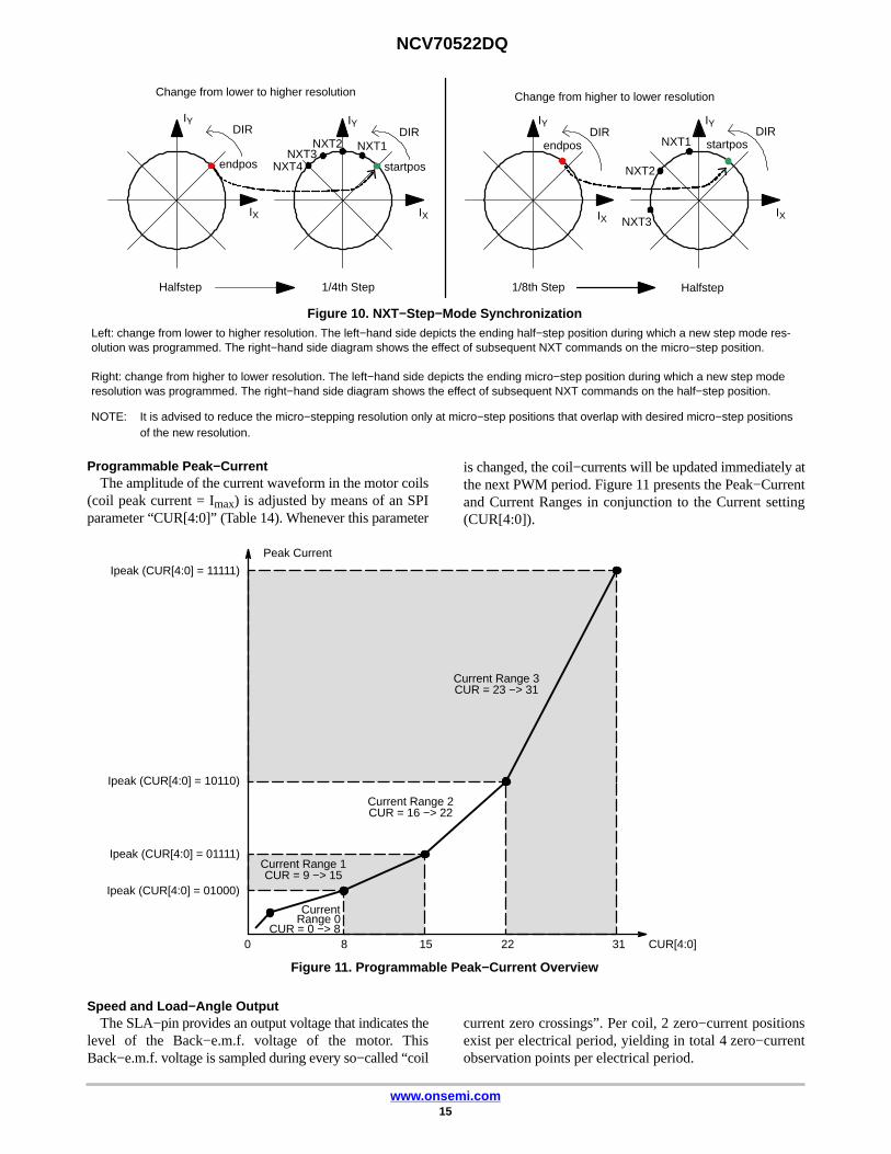
Programmable Peak−CurrentThe amplitude of the current waveform in the motor coils
(coil peak current = Imax) is adjusted by means of an SPIparameter “CUR[4:0]” (Table 14). Whenever this parameter
is changed, the coil−currents will be updated immediately atthe next PWM period. Figure 11 presents the Peak−Currentand Current Ranges in conjunction to the Current setting(CUR[4:0]).
Peak Current
Ipeak (CUR[4:0] = 11111)
Ipeak (CUR[4:0] = 10110)
Ipeak (CUR[4:0] = 01111)
Ipeak (CUR[4:0] = 01000)
0 8 15 22 31 CUR[4:0]
Current Range 3CUR = 23 −> 31
Current Range 2CUR = 16 −> 22
Current Range 1CUR = 9 −> 15
Current
CUR = 0 −> 8
Figure 11. Programmable Peak−Current Overview
Range 0
Speed and Load−Angle OutputThe SLA−pin provides an output voltage that indicates the
level of the Back−e.m.f. voltage of the motor. ThisBack−e.m.f. voltage is sampled during every so−called “coil
current zero crossings”. Per coil, 2 zero−current positionsexist per electrical period, yielding in total 4 zero−currentobservation points per electrical period.

NCV70522DQ
www.onsemi.com16
Figure 12. Principle of Bemf Measurement
Current DecayZero Current
Voltage Transient
ZOOM
PreviousMicro−Step Coil Current Zero Crossing Next
Micro−Step
t
ICOILVBEMF
ICOIL
VCOIL
VBB|VBEMF|
t
t
Because of the relatively high re−circulation currents inthe coil during current decay, the coil voltage VCOIL showsa transient behavior. As this transient is not always desiredin application software, two operating modes can be selectedby means of the bit <SLAT> (see “SLA−transparency” inTable 12). The SLA pin shows in “transparent mode” fullvisibility of the voltage transient behavior. This allows asanity−check of the speed−setting versus motor operationand characteristics and supply voltage levels. If the bit“SLAT” is cleared, then only the voltage samples at the endof each coil current zero crossing are visible on the
SLA−pin. Because the transient behavior of the coil voltageis not visible anymore, this mode generates smoother Backe.m.f. input for post−processing, e.g. by software.
In order to bring the sampled Back e.m.f. to a descentoutput level (0 V to 5 V), the sampled coil voltage VCOIL isdivided by 2 or by 4. This divider is set through a SPI bit<SLAG>. (See Table 12)
The following drawing illustrates the operation of theSLA−pin and the transparency−bit. “PWMsh” and“Icoil=0” are internal signals that define together with SLATthe sampling and hold moments of the coil voltage.

NCV70522DQ
www.onsemi.com17
PWMsh
SLAT
SLA−Pin last
retainedretain last sampleprevious output is
bufSsh Sh
ChCsh
SLATNOT (Icoil=0)
Icoil=0PWMsh
SLA−Pindiv2div4
t
t
Figure 13. Timing Diagram of SLA−Pin
SLAT = 1 => SLA−pin is “transparent” duringVBEMF sampling @ Coil Current ZeroCrossing. SLA−pin is updated “real−time”.
SLAT = 0 => SLA−pin is not “transparent”during VBEMF sampling @ Coil Current ZeroCrossing. SLA−pin is updated when leavingcurrent−less state.
VCOIL
VCOIL
VBEMFsampleis
kept at SLA pin
Icoil=0
Warning, Error Detection and Diagnostics Feedback
Thermal Warning and ShutdownWhen Junction temperature rises above TTW, the thermal
warning bit <TW> is set (Table 16 SPI Status Register 0). Ifjunction temperature increases above thermal shutdownlevel, then the circuit goes in “Thermal Shutdown” mode(<TSD>) and all driver transistors are disabled (highimpedance) (Table 16 SPI Status Register 2). The conditionsto reset flag <TSD> is to be at a temperature lower than TTWand to clear the <TSD> flag by reading it using any SPI readcommand.
Overcurrent DetectionThe overcurrent detection circuit monitors the load
current in each activated output stage. If the load currentexceeds the overcurrent detection threshold, then theovercurrent flag is set and the drivers are switched off toreduce the power dissipation and to protect the integratedcircuit. Each driver transistor has an individual detection bitin the Table 16 SPI Status Registers 1 and SPI StatusRegister 2 (<OVCXij> and <OVCYij>). Error condition islatched and the microcontroller needs to clear the status bitsto reactivate the drivers.
Note: Successive reading the SPI Status Registers 1 and 2 incase of a short circuit condition, may lead to damage to thedrivers.
Open Coil DetectionOpen coil detection is based on the observation of 100%
duty cycle of the PWM regulator. If in a coil 100% duty cycleis detected for longer than 32 ms the appropriate status bit inthe SPI status register is set (<OPENX> or <OPENY>).(Table 16: SPI Status Register 0).
When the resistance of a motor coil is very large and thebattery voltage is low, it can happen that the motor driver isnot able to deliver the requested current to the motor. Underthese conditions the PWM controller duty cycle will be100% and after 32 ms, the error pin and <OPENX>,<OPENY> will flag this situation (motor current is keptalive). This feature can be used to test if the operatingconditions (supply voltage, motor coil resistance) still allowreaching the requested coil−current or else the coil−currentshould be reduced.

NCV70522DQ
www.onsemi.com18
Charge Pump FailureThe charge pump is an important circuit that guarantees
low RDS(on) for all drivers, especially for low supplyvoltages. If the supply voltage is too low or externalcomponents are not properly connected to guarantee RDS(on)of the drivers, then the bit <CPFAIL> is set in the SPI StatusRegister 0. Also after power−on−reset the charge pumpvoltage will need some time to exceed the requiredthreshold. During that time <CPFAIL> will be set to “1”.
Error OutputThis is an open drain digital output to flag a problem to the
external microcontroller. The signal on this output is activelow and the logic combination of:
NOT(ERR) = <TW> OR <TSD> OR <OVCXij> OR<OVCYij> OR <OPENi> OR <CPFAIL>
Logic Supply RegulatorThe NCV70522DQ has an on−chip 5 V low−drop
regulator with external capacitor to supply the digital part ofthe chip, some low−voltage analog blocks and externalcircuitry. The voltage level is derived from an internalbandgap reference. To calculate the available drive−currentfor external circuitry, the specified Iload should be reducedwith the consumption of internal circuitry (unloadedoutputs) and the loads connected to logic outputs. SeeTable 5.
Power−On Reset (POR) FunctionThe open drain output pin POR/WD provides an “active
low” reset for external purposes. At powerup ofNCV70522DQ, this pin will be kept low for some time toreset for example an external microcontroller. A smallanalog filter avoids resetting due to spikes or noise on theVDD supply.
Figure 14. Power−on−Reset Timing Diagram
VBB
VDD
t
t
VDDH
VDDL
POR/WD pin
tPU tPD
< tRF
tPOR tRF
Watchdog FunctionThe watchdog function is enabled/disabled through
<WDEN> bit (Table 13). Once this bit has been set to “1”(watchdog enable), the microcontroller needs to re−writethis bit to clear an internal timer before the watchdog timeoutinterval expires. In case the timer is activated and WDEN is
acknowledged too early (before tWDPR) or not within theinterval (after tWDTO), then a reset of the microcontrollerwill occur through POR/WD pin. In addition, a warm/coldboot bit <WD> is available in Table 16 for further processingwhen the external microcontroller is alive again.

NCV70522DQ
www.onsemi.com19
VBB
VDD
t
t
Enable WD
Acknowledge WD
WD timer t
t
Figure 15. Watchdog Timing Diagram
VDDH
tPU
tPOR
tDSPI
POR/WD pin
tWDTO
tPORtWDRD
= tWDPR or = tWDTO> tWDPR and < tWDTO
Note: tDSPI is the time needed by the externalmicrocontroller to shift−in the <WDEN> bit after apower−up.
The duration of the watchdog timeout interval isprogrammable through the WDT[3:0] bits. The timing isgiven in Figure 15.
CLR Pin (=Hard Reset)Logic 0 on CLR pin allows normal operation of the chip.
To reset the complete digital inside the NCV70522DQ, theinput CLR needs to be pulled to logic 1 during minimumtime given by tCLR. (See AC Parameters) This reset functionclears all internal registers without the need of apower−cycle, except in sleep mode. The operation of allanalog circuits is depending on the reset state of the digital,charge pump remains active. Logic 0 on CLR pin resumesnormal operation again. The voltage regulator remainsfunctional during and after the reset and the POR/WD pin isnot activated. Watchdog function is reset completely.
Sleep ModeThe bit <SLP> in SPI Control Register 2 is provided to
enter a so−called “sleep mode”. This mode allows reductionof current−consumption when the motor is not in operation.The effect of sleep mode is as follows:• The drivers are put in HiZ
• All analog circuits are disabled and in low−power mode
• All internal registers are maintaining their logic content
• NXT and DIR inputs are ignored
• SPI communication remains possible (slight currentincrease during SPI communication)
• Oscillator and digital clocks are silent, except duringSPI communication
Normal operation is resumed after writing logic ‘0’ to bit<SLP>. A start−up time is needed for the charge pump tostabilize. After this time, NXT commands can be issued.When the device is in sleep mode and VBB becomes lowerthan VBB_min the device might reset.

NCV70522DQ
www.onsemi.com20
SPI INTERFACE
The serial peripheral interface (SPI) allows an externalmicrocontroller (Master) to communicate with theNCV70522DQ. The implemented SPI block is designed tointerface directly with numerous micro−controllers fromseveral manufacturers. The NCV70522DQ acts always as aSlave and cannot initiate any transmission. The operation ofthe device is configured and controlled by means of SPIregisters which are observable for read and/or write from theMaster.
SPI Transfer Format and Pin SignalsDuring a SPI transfer, data is simultaneously transmitted
(shifted out serially) and received (shifted in serially). Aserial clock line (CLK) synchronizes shifting and samplingof the information on the two serial data lines (DO and DI).
DO signal is the output from the Slave (NCV70522DQ), andDI signal is the output from the Master. A chip select line(CS) allows individual selection of a Slave SPI device in amultiple− slave system. The CS line is active low. If theNCV70522DQ is not selected, DO is pulled up with theexternal pullup resistor. Since NCV70522DQ operates as aSlave in MODE 0 (CPOL = 0; CPHA = 0) it always clocksdata out on the falling edge and samples data in on risingedge of clock. The Master SPI port must be configured inMODE 0 too, to match this operation. The SPI clock idleslow between the transferred bytes.
The diagram below is both a Master and a Slave timingdiagram since CLK, DO and DI pins are directly connectedbetween the Master and the Slave.
ÌÌÌÌÌÌ
ÌÌÌÌÌÌÌÌ
DI MSB
CLK
1 2 3 4 5 6 7 8
DO
#CLK Cycle
MSB
LSB
LSB
6 5 4 3 2 1
6 5 4 3 2 1
Figure 16. Timing Diagram of a SPI Transfer
CS
NOTE: At the falling edge of the eighth clock pulse the data−out shift register is updated with the content of the addressed internal SPIregister. The internal SPI registers are updated at the first rising edge of the NCV70522DQ system clock when CS = High.
Transfer PacketSerial data transfer is assumed to follow MSB first rule. The transfer packet contains one or more bytes.
LSB
DataCommand and SPI Register Address
CMD2 CMD1 CMD0 ADDR4 ADDR3 ADDR2 ADDR1 ADDR0 D7 D6 D5 D4 D3 D2 D1 D0
MSBLSBMSB
BYTE 1 BYTE 2
Command SPI Register Address
Figure 17. SPI Transfer Packet
Byte 1 contains the Command and the SPI RegisterAddress and indicates to the NCV70522DQ the chosen typeof operation and addressed register. Byte 2 contains data, orsent from the Master in a WRITE operation, or receivedfrom the NCV70522DQ in a READ operation.
Two command types can be distinguished in thecommunication between Master and NCV70522DQ:• READ from SPI Register with address ADDR[4:0]:
CMD[2:0] = “000”• WRITE to SPI Register with address ADDR[4:0]:
CMD[2:0] = “100”

NCV70522DQ
www.onsemi.com21
READ OperationIf the Master wants to read data from Status or Control
Registers, it initiates the communication by sending aREAD command. This READ command contains theaddress of the SPI register to be read out. At the falling edgeof the eighth clock pulse the data−out shift register is
updated with the content of the corresponding internal SPIregister. In the next 8−bit clock pulse train this data is shiftedout via DO pin. At the same time the data shifted in from DI(Master) should be interpreted as the following successivecommand or dummy data.
Figure 18. Single READ Operation where DATA from SPI Register with Address 1 is Read by the Master
DATA from previous command orNOT VALID after POR or RESET
Registers are updated with the internal status at the rising edgeof the internal NCV70522DQ clock when CS = 1
READ DATA from ADDR1 COMMAND or DUMMY
OLD DATA or NOT VALID DATA from ADDR1
COMMAND
DATA DATA
DO
DI
CS
All 4 Status Registers (see SPI Registers) contain 7 databits and an even parity check bit. The most significant bit(D7) represents a parity of D[6:0]. If the number of logicalones in D[6:0] is odd, the parity bit D7 equals “1”. If thenumber of logical ones in D[6:0] is even then the parity bitD7 equals “0”. This simple mechanism protects againstnoise and increases the consistency of the transmitted data.If a parity check error occurs it is recommended to initiatean additional READ command to obtain the status again.
Also the Control Registers can be read out following thesame routine. Control Registers don’t have a parity check.
The CS line is active low and may remain low betweensuccessive READ commands as illustrated in Figure 20.There is however one exception. In case an error conditionis latched in one of Status Registers (see SPI Registers) theERR pin is activated. (See the “Error Output” Section). Thissignal flags a problem to the external microcontroller. Byreading the Status Registers information, the root cause ofthe problem can be determined. After this READ operationthe Status Registers are cleared. Because the StatusRegisters and ERR pin (see SPI Registers) are only updatedby the internal system clock when the CS line is high, the
Master should force CS high immediately after the READoperation. For the same reason it is recommended to keepthe CS line high always when the SPI bus is idle.
WRITE OperationIf the Master wants to write data to a Control Register it
initiates the communication by sending a WRITEcommand. This contains the address of the SPI register towrite to. The command is followed with a data byte. Thisincoming data will be stored in the corresponding ControlRegister after CS goes from low to high! NCV70522DQresponds on every incoming byte by shifting out via DO thedata stored in the last received address.
It is important that the writing action (command − addressand data) to the Control Register is exactly 16 bits long. Ifmore or less bits are transmitted the complete transfer packetis ignored.
A WRITE command executed for a read−only register(e.g. Status Registers) will not affect the addressed registerand the device operation.
Because after a power−on−reset the initial address isunknown the data shifted out via DO is not valid.
DATA from previous command orNOT VALID after POR or RESET
DO
DI
CS
WRITE DATA to ADDR3 NEW DATA for ADDR3
OLD DATA or NOT VALID OLD DATA from ADDR3
COMMAND
DATA DATA
DATA
The NEW DATA is written into the correspondinginternal register at the rising edge of CS
Figure 19. Single WRITE Operation where DATA from the Master is Written in SPI Register with Address 3

NCV70522DQ
www.onsemi.com22
Examples of Combined READ and WRITE OperationsIn the following examples successive READ and WRITE
operations are combined. In Figure 20 the Master first readsthe status from Register at ADDR4 and at ADDR5 followed
by writing a control byte in Control Register at ADDR2.Note that during the write command (in Figures 19 and 20)the old data of the pointed register is returned at the momentthe new data is shifted in.
Figure 20. Two Successive READ Commands Followed by a WRITE Command
COMMAND COMMAND COMMAND DATA
DATA DATA DATA DATA
DO
DI
CS
DATA from previouscommand or NOT VALID
after POR or RESET
READ DATAfrom ADDR4
READ DATAfrom ADDR5
WRITE DATAto ADDR2
NEW DATAfor ADDR2
OLD DATAor NOT VALID
DATAfrom ADDR4
DATAfrom ADDR5
OLD DATAfrom ADDR2
Registers are updated with the internal status at the risingedge of the internal NCV70522DQ clock when CS = 1
The NEW DATA is written into the correspondinginternal register at the rising edge of CS
After the write operation the Master could initiate a readback command in order to verify if the data is correctlywritten, as illustrated in Figure 21. During reception of theREAD command the old data is returned for a second time.Only after receiving the READ command the new data is
transmitted. This rule also applies when the master devicewants to initiate an SPI transfer to read the Status Registers.Because the internal system clock updates the StatusRegisters only when CS line is high, the first read out bytemight represent old status information.
COMMAND
DATA DATA DATA DATA
OLD DATAor NOT VALID
OLD DATAfrom ADDR2
OLD DATAfrom ADDR2
NEW DATAfrom ADDR2DO
DI
CS
Figure 21. A WRITE Operation where DATA from the Master is Written in SPI Register with Address 2 Followed bya READ Back Operation to Verify a Correct WRITE Operation
DATA COMMAND
WRITE DATAto ADDR2
NEW DATAfor ADDR2
READ DATAfrom ADDR2
COMMAND orDUMMY
Registers are Updated with the InternalStatus at the Rising Edge of CS
Registers are Updated with the In-ternal Status at the Rising Edge ofthe Internal NCV70522DQ Clockwhen CS = 1
DATA from previouscommand or NOT VALID
after POR or RESET
NOTE: The internal data−out shift buffer of the NCV70522DQ is updated with the content of the selected SPI register only at the last (everyeighth) falling edge of the CLK signal (see SPI Transfer Format and Pin Signals). As a result, new data for transmission cannot bewritten to the shift buffer at the beginning of the transfer packet and the first byte shifted out might represent old data.
Table 11. SPI CONTROL REGISTERS(All SPI Control Registers have Read/Write Access and default to “0” after Power−on or hard reset)
Address
Content
Structure
Bit 7 Bit 6 Bit 5 Bit 4 Bit 3 Bit 2 Bit 1 Bit 0
Access R/W R/W R/W R/W R/W R/W R/W R/W
Reset 0 0 0 0 0 0 0 0
CRWD (00h) Data WDEN WDT[3:0] 0 0 0
CR0 (01h) Data SM[2:0] CUR[4:0]
CR1 (02h) Data DIRCTRL NXTP − − PWMF PWMJ EMC[1:0]
CR2 (03h) Data MOTEN SLP SLAG SLAT − − − −
Where:R/W: Read and Write accessReset: Status after Power−On or hard resetWDEN: Watchdog enable. Writing “0” to this bit will clear WD bit (see SPI Status Register 0)WDT[3:0]: Watchdog timeout interval

NCV70522DQ
www.onsemi.com23
Table 12. SPI CONTROL PARAMETER OVERVIEW
Symbol Description Status Value
WDEN Watchdog enable.<WDEN> = 1
Writing “1” to this bit will enable the watchdog timer (if notenabled yet) or will clear this timer (if already enabled)
<WDEN> = 0 Writing “0” to this bit will disable the Watchdog
DIRCTRLControls the Direction of Rotation(in Combination with Logic Levelon Input DIR)
<DIR> = 0<DIRCTRL> = 0 CW Motion
<DIRCTRL> = 1 CCW Motion
<DIR> = 1<DIRCTRL> = 0 CCW Motion
<DIRCTRL> = 1 CW Motion
EMC[1:0]Turn On− and Turn−off Slopes(Note 15)
00 Very Fast
01 Fast
10 Slow
11 Very Slow
MOTEN Activates the Motor Driver Outputs<MOTEN> = 0 Drivers Disabled
<MOTEN> = 1 Drivers Enabled
NXTPSelects if NXT triggers on Risingor Falling Edge
<NXTP> = 0 Trigger on Rising Edge
<NXTP> = 1 Trigger on Falling Edge
PWMFEnables Doubling of the PWMFrequency (Note 15)
<PWMF> = 0 Default Frequency
<PWMF> = 1 Double Frequency
PWMJ Enables Jitter PWM<PWMJ> = 0 Jitter Disabled
<PWMJ> = 1 Jitter Enabled
SM[2:0] Stepmode
000 1/32 Micro Step
001 1/16 Micro Step
010 1/8 Micro Step
011 1/4 Micro Step
100 1/2 Compensated Half Step
101 1/2 Uncompensated Half Step
110 Full Step
111 n.a.
SLAG Speed Load Angle Gain Setting<SLAG> = 0 Gain = 0.5
<SLAG> = 1 Gain = 0.25
SLATSpeed Load AngleTransparency Bit
<SLAT> = 0 SLA is NOT Transparent
<SLAT> = 1 SLA is Transparent
SLP Enables Sleep Mode<SLP> = 0 Active Mode
<SLP> = 1 Sleep Mode
15.The typical values can be found in Table 5: DC Parameters and Table 6: AC Parameters
NCV70522DQ
www.onsemi.com24
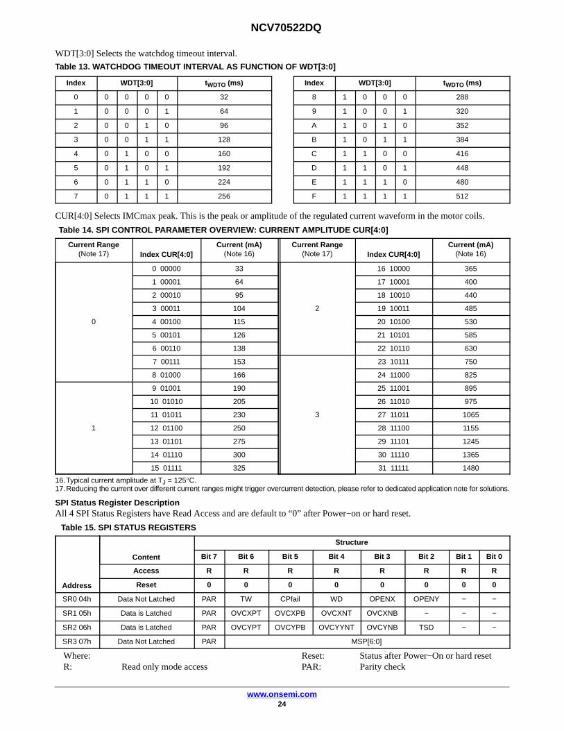
WDT[3:0] Selects the watchdog timeout interval.
Table 13. WATCHDOG TIMEOUT INTERVAL AS FUNCTION OF WDT[3:0]
Index WDT[3:0] tWDTO (ms)
0 0 0 0 0 32
1 0 0 0 1 64
2 0 0 1 0 96
3 0 0 1 1 128
4 0 1 0 0 160
5 0 1 0 1 192
6 0 1 1 0 224
7 0 1 1 1 256
Index WDT[3:0] tWDTO (ms)
8 1 0 0 0 288
9 1 0 0 1 320
A 1 0 1 0 352
B 1 0 1 1 384
C 1 1 0 0 416
D 1 1 0 1 448
E 1 1 1 0 480
F 1 1 1 1 512
CUR[4:0] Selects IMCmax peak. This is the peak or amplitude of the regulated current waveform in the motor coils.
Table 14. SPI CONTROL PARAMETER OVERVIEW: CURRENT AMPLITUDE CUR[4:0]
Current Range(Note 17) Index CUR[4:0]
Current (mA)(Note 16)
Current Range(Note 17) Index CUR[4:0]
Current (mA)(Note 16)
0
0 00000 33
2
16 10000 365
1 00001 64 17 10001 400
2 00010 95 18 10010 440
3 00011 104 19 10011 485
4 00100 115 20 10100 530
5 00101 126 21 10101 585
6 00110 138 22 10110 630
7 00111 153
3
23 10111 750
8 01000 166 24 11000 825
1
9 01001 190 25 11001 895
10 01010 205 26 11010 975
11 01011 230 27 11011 1065
12 01100 250 28 11100 1155
13 01101 275 29 11101 1245
14 01110 300 30 11110 1365
15 01111 325 31 11111 1480
16.Typical current amplitude at TJ = 125°C.17.Reducing the current over different current ranges might trigger overcurrent detection, please refer to dedicated application note for solutions.
SPI Status Register DescriptionAll 4 SPI Status Registers have Read Access and are default to “0” after Power−on or hard reset.
Table 15. SPI STATUS REGISTERS
Address
Content
Structure
Bit 7 Bit 6 Bit 5 Bit 4 Bit 3 Bit 2 Bit 1 Bit 0
Access R R R R R R R R
Reset 0 0 0 0 0 0 0 0
SR0 04h Data Not Latched PAR TW CPfail WD OPENX OPENY − −
SR1 05h Data is Latched PAR OVCXPT OVCXPB OVCXNT OVCXNB − − −
SR2 06h Data is Latched PAR OVCYPT OVCYPB OVCYYNT OVCYNB TSD − −
SR3 07h Data Not Latched PAR MSP[6:0]
Where:R: Read only mode access
Reset: Status after Power−On or hard resetPAR: Parity check

NCV70522DQ
www.onsemi.com25
Table 16. SPI STATUS FLAGS OVERVIEW
Mnemonic FlagLength
(bit)Related
SPI Register CommentResetState
CPFail Charge Pump Failure 1 Status Register 0‘0’ = no failure‘1’ = failure: indicates that the charge pump does notreach the required voltage level.
‘0’
WD Watchdog event 1 Status Register 0
This bit indicates the watchdog timer has not beencleared properly in time. If the master reads that WDis set to “1” after reset, it means that a watchdog re-set occurred (warm boot) instead of power−on−reset(cold boot). WD bit will be cleared only when themaster writes “0” to WDEN bit.
‘0’
MSP[6:0] Micro Step Position 7 Status Register 3 Translator micro step position ‘0000000’
OPENX OPEN Coil X 1 Status Register 0 ‘1’ = Open coil detected ‘0’
OPENY OPEN Coil Y 1 Status Register 0 ‘1’ = Open coil detected ‘0’
OVCXNBOvercurrent at
MOTXN Terminal;Bottom Transistor
1 Status Register 1‘0’ = no failure‘1’ = failure: indicates that overcurrent is detected atbottom transistor XN−terminal
‘0’
OVCXNTOvercurrent at
MOTXN Terminal;Top Transistor
1 Status Register 1‘0’ = no failure‘1’ = failure: indicates that overcurrent is detected attop transistor XN−terminal
‘0’
OVCXPBOvercurrent at
MOTXP Terminal;Bottom Transistor
1 Status Register 1‘0’ = no failure‘1’ = failure: indicates that overcurrent is detected atbottom transistor XP−terminal
‘0’
OVCXPTOvercurrent at
MOTXP Terminal;Top Transistor
1 Status Register 1‘0’ = no failure‘1’ = failure: indicates that overcurrent is detected attop transistor XP−terminal
‘0’
OVCYNBOvercurrent at
MOTYN Terminal;Bottom Transistor
1 Status Register 2‘0’ = no failure‘1’ = failure: indicates that overcurrent is detected atbottom transistor YN−terminal
‘0’
OVCYNTOvercurrent at
MOTYN Terminal;Top Transistor
1 Status Register 2‘0’ = no failure‘1’ = failure: indicates that overcurrent is detected attop transistor YN−terminal
‘0’
OVCYPBOvercurrent at
MOTYP Terminal;Bottom Transistor
1 Status Register 2‘0’ = no failure‘1’ = failure: indicates that overcurrent is detected atbottom transistor YP−terminal
‘0’
OVCYPTOvercurrent at
MOTYP Terminal;Top Transistor
1 Status Register 2‘0’ = no failure‘1’ = failure: indicates that overcurrent is detected attop transistor YP−terminal
‘0’
TSD Thermal Shutdown 1 Status Register 2 ‘0’
TW Thermal Warning 1 Status Register 0 ‘0’
WD Watchdog event 1 Status Register 0‘0’ = no watchdog reset‘1’ = watchdog reset occurred ‘0’

NCV70522DQ
www.onsemi.com26
PACKAGE DIMENSIONS
ÉÉÉÉÉÉÉÉÉ
SSOP36 EPCASE 940AB
ISSUE O
DIM MIN MAXMILLIMETERS
E2 3.90 4.10
A 2.65A1 --- 0.10
L 0.50 0.90
e 0.50 BSC
c 0.23 0.32
h 0.25 0.75
b 0.18 0.36
D2 5.70 5.90
L2 0.25 BSCM 0 8 � �
NOTES:1. DIMENSIONING AND TOLERANCING PER
ASME Y14.5M, 1994.2. CONTROLLING DIMENSION: MILLIMETERS.3. DIMENSION b DOES NOT INCLUDE DAMBAR
PROTRUSION. ALLOWABLE DAMBARPROTRUSION SHALL BE 0.13 TOTAL INEXCESS OF THE b DIMENSION AT MMC.
4. DIMENSION b SHALL BE MEASURED BE-TWEEN 0.10 AND 0.25 FROM THE TIP.
5. DIMENSIONS D AND E1 DO NOT INCLUDEMOLD FLASH, PROTRUSIONS OR GATEBURRS. DIMENSIONS D AND E1 SHALL BEDETERMINED AT DATUM H.
6. THIS CHAMFER FEATURE IS OPTIONAL. IFIT IS NOT PRESENT, A PIN ONE IDENTIFIERMUST BE LOACATED WITHIN THE INDIC-ATED AREA.
PIN 1REFERENCE
D
E1
0.10SEATINGPLANE
36X b
E
e
DETAIL A
---
SOLDERING FOOTPRINT
L
L2
GAUGE
DETAIL A
e/2
DETAIL B
A2 2.35 2.60
E1 7.50 BSC
PLANE
SEATINGPLANEC
X
c
h
END VIEW
AM0.25 BTTOP VIEW
SIDE VIEW
A-B0.20 C
1 18
1936A
B
DDETAIL B
36X
A1
A2
C
C
D2
E2
BOTTOM VIEW
36X
D 10.30 BSC
E 10.30 BSC
M1 5 15 � �
5.90 36X1.06
36X0.360.50
DIMENSIONS: MILLIMETERSPITCH
4.10 10.76
1
0.25 C
S S
4X
H A
X = A or B
h
NOTE 6
M1
M
36X

NCV70522DQ
www.onsemi.com27
DEVICE ORDERING INFORMATION
Part NumberAmbient
Temperature Range Package TypePeak
Current Shipping†
NCV70522DQ004R2G −40°C to +125°C SSOP36−EP(Pb−Free)
1500 mA 1500 / Tape & Reel
NCV70522DQ004G −40°C to +125°C SSOP36−EP(Pb−Free)
1500 mA 47 / Tube / Tray
†For information on tape and reel specifications, including part orientation and tape sizes, please refer to our Tape and Reel PackagingSpecifications Brochure, BRD8011/D.
ON Semiconductor and are registered trademarks of Semiconductor Components Industries, LLC (SCILLC). SCILLC reserves the right to make changes without further noticeto any products herein. SCILLC makes no warranty, representation or guarantee regarding the suitability of its products for any particular purpose, nor does SCILLC assume any liabilityarising out of the application or use of any product or circuit, and specifically disclaims any and all liability, including without limitation special, consequential or incidental damages.“Typical” parameters which may be provided in SCILLC data sheets and/or specifications can and do vary in different applications and actual performance may vary over time. Alloperating parameters, including “Typicals” must be validated for each customer application by customer’s technical experts. SCILLC does not convey any license under its patent rightsnor the rights of others. SCILLC products are not designed, intended, or authorized for use as components in systems intended for surgical implant into the body, or other applicationsintended to support or sustain life, or for any other application in which the failure of the SCILLC product could create a situation where personal injury or death may occur. ShouldBuyer purchase or use SCILLC products for any such unintended or unauthorized application, Buyer shall indemnify and hold SCILLC and its officers, employees, subsidiaries, affiliates,and distributors harmless against all claims, costs, damages, and expenses, and reasonable attorney fees arising out of, directly or indirectly, any claim of personal injury or deathassociated with such unintended or unauthorized use, even if such claim alleges that SCILLC was negligent regarding the design or manufacture of the part. SCILLC is an EqualOpportunity/Affirmative Action Employer. This literature is subject to all applicable copyright laws and is not for resale in any manner.
PUBLICATION ORDERING INFORMATIONN. American Technical Support: 800−282−9855 Toll FreeUSA/Canada
Europe, Middle East and Africa Technical Support:Phone: 421 33 790 2910
Japan Customer Focus CenterPhone: 81−3−5817−1050
NCV70522DQ/D
LITERATURE FULFILLMENT:Literature Distribution Center for ON SemiconductorP.O. Box 5163, Denver, Colorado 80217 USAPhone: 303−675−2175 or 800−344−3860 Toll Free USA/CanadaFax: 303−675−2176 or 800−344−3867 Toll Free USA/CanadaEmail: [email protected]
ON Semiconductor Website: www.onsemi.com
Order Literature: http://www.onsemi.com/orderlit
For additional information, please contact your localSales Representative