unipolar 2-phase stepping motor driver ics · 2019-07-29 · 6 sanken electric co., ltd. 28610.23,...
TRANSCRIPT

SANKEN ELECTRIC CO., LTD.http://www.sanken-ele.co.jp/en/
SLA7080M Series
DescriptionThis document describes the function and features of SLA7080M series, which are unipolar 2-phase stepping motor driver ICs. Four levels of output current are available from the incorporated MOSFETs, corresponding to the rated output current ratings. All current ratings are available with protection against motor coil shorts or motor open wire detection.
The SLA7080M series has a multichip structure, for enhanced thermal dispersion. The Control IC (MIC), four power elements (MOSFET), and dual sense resistors, are all separate ICs.
Built-in sense resistors for each phase allow accurate track-ing of performance without additional external components. Low-power sleep mode as well as reduced power during PWM off-time maximize energy savings.
Features and Benefits▪ Power supply voltage, VBB , 46 V maximum; 10 to 44 V
normal operating range▪ Logic supply voltage, VDD , 3 to 5.5 V▪ Four output currents, IO(max) , options: 1, 1.5, 2, and 3 A▪ Stepping control for phase input (full or half step)▪ Built-in sense resistor detects motor current▪ Compact ZIP 23-pin molded package (SLA package)▪ Self-excitation PWM control with fixed off-time▪ Built-in synchronous rectifying circuit reduces losses at
PWM-off▪ Synchronous PWM function prevents noise generation in
motor Hold mode▪ Sleep function reduces power consumption of drivers in
Standby mode▪ Protection circuit detects motor coil open/short and
prevents overheating due to avalanche breakdown▪ Externally-adjustable (3.2 μs /5.2 μs) blanking time
(minimum on-time)
Unipolar 2-Phase Stepping Motor Driver ICs
Functional Block Diagram
Package: 23-pin ZIP (type SLA)
Not to scale
Logic Block
SynchroControlPWM
ControlOSC
Comp+
-
Pre-Driver
Protect
PWMControl
OSC
Pre-Driver
Protect
Comp+
-
MICReg.
OU
TA
OU
TA
OU
TB
OU
TB
OU
TB
OU
TB
OU
TA
OU
TA
VD
D
RE
F/SLE
EP
B_SEL
INB
INB
INA
INA
FLAG
VBB
SENSEBSENSEA
GNDSYNC
Rs Rs
28610.23, Rev. 1
2SANKEN ELECTRIC CO., LTD.
28610.23, Rev. 1
Unipolar 2-Phase Stepping Motor Driver ICsSLA7080M Series
Absolute Maximum Ratings, valid at TA = 25°CCharacteristic Symbol Notes Rating Unit
Motor Supply Voltage VM 46 V
Main Supply Voltage VBB 46 V
Logic Supply Voltage VDD 6 V
Output Current IO
SLA7080MPR 1.0 A
SLA7081MPR 1.5 A
SLA7082MPR 2.0 A
SLA7083MPR 3.0 A
Logic Input Voltage VIN –0.3 to VDD + 0.3 V
REF Input Voltage VREF –0.3 to VDD + 0.3 V
Allowable Power Dissipation PD No heatsink 4.7 W
Maximum Junction Temperature TJ(max) 150 ºC
Nominal Operating Temperature TA –20 to 85 ºC
Storage Temperature Tstg –30 to 150 ºC
All performance characteristics given are typical values for circuit or system baseline design only and are at the nominal operating voltage and an ambient temperature, TA, of 25°C, unless oth er wise stated.
Selection Guide
Part Number Output Current(A)
Built-In Sense Resistor Packing
SLA7080MPR 1
Yes 18 pieces per tubeSLA7081MPR 1.5
SLA7082MPR 2
SLA7083MPR 3
Recommended Operating RangeCharacteristic Symbol Notes Min Max Unit
Motor Supply Voltage VM – 44 V
Main Supply Voltage VBB 10 44 V
Logic Supply Voltage VDD VDD surge voltage = ± 0.5 V 3.0 5.5 V
Case Temperature TCWithout heatsink On pin 12, adjacent
to case – 90 ºC
With heatsink – 80 ºC

3SANKEN ELECTRIC CO., LTD.
28610.23, Rev. 1
Unipolar 2-Phase Stepping Motor Driver ICsSLA7080M Series
ELECTRICAL CHARACTERISTICS valid at TA = 25°C, VBB = 24 V and VDD = 5 V, unless otherwise notedCharacteristics Symbol Conditions Min Typ Max Units
Main Supply CurrentIBB In operation – – 15 mA
IBBS Sleep state – – 100 μA
Logic Supply Current IDD – – 5 mA
Output MOSFET On-Resistance RDS(on)
SLA7080MPR – 0.7 0.85 Ω
SLA7081MPR – 0.45 0.6 Ω
SLA7082MPR – 0.25 0.4 Ω
SLA7083MPR – 0.18 0.24 Ω
Output MOSFET Diode Forward Voltage VF
SLA7080MPR – 0.85 1.1 V
SLA7081MPR – 1.0 1.25 V
SLA7082MPR – 0.95 1.2 V
SLA7083MPR – 0.95 2.1 V
Output MOSFET Breakdown Voltage VDSS VBB = 44 V, ID = 1 mA 100 – – V
Maximum Response Frequency fclk Clock duty cycle = 50% 250 – – kHz
Logic Input VoltageVIL – – VDD ×
0.25 V
VIHVDD × 0.75 – – V
Logic Input CurrentIIL – ±1 – μA
IIH – ±1 – μA
REF Input VoltageVREF
SLA7080MPR 0.04 – 0.3 V
SLA7081MPR, SLA7083MPR 0.04 – 0.45 V
SLA7082MPR 0.04 – 0.4 V
VREFS Sleep state (output off) 2.0 – VDD V
REF Input Current IREF – ±10 – μA
SENSE Detect Voltage VSENSEVREF – 0.03 VREF
VREF + 0.03 V
Sense Resistor1 Rs
SLA7080MPR, SLA7081MPR 0.296 0.305 0.314 Ω
SLA7082MPR 0.199 0.205 0.211 Ω
SLA7083MPR 0.150 0.155 0.160 Ω
PWM Minimum On-Time (Blanking Time) ton(min)
B_SEL = low – 3.2 – μs
B_SEL = high – 5.2 – μs
PWM Off-Time toff – 13 – μs
Sleep Enable Recovery Time tSE Sleep state 100 – – μs
Switching Timetdon Phase INx → Phase OUTx on – 1.5 – μs
tdoff Phase INx → Phase OUTx off – 1.0 – μs
Continued on the next page…

4SANKEN ELECTRIC CO., LTD.
28610.23, Rev. 1
Unipolar 2-Phase Stepping Motor Driver ICsSLA7080M Series
ELECTRICAL CHARACTERISTICS (continued) valid at TA = 25°C, VBB = 24 V and VDD = 5 V, unless otherwise notedCharacteristics Symbol Conditions Min Typ Max Units
Power Derating Chart
Allo
wab
le P
ower
Dis
sipa
tion,
PD
(W)
Ambient Temperature, TA (°C)
5
4
3
2
1
00 10 20 30 40 50 60 70 80 90
RθJA = 26.6°C/W
Protection Functions2
Overcurrent Detect Voltage VOCP At motor coil short circuit 0.65 0.7 0.75 V
Overcurrent Detect Current (VOCP / RS) IOCP
SLA7080MPR, SLA7081MPR – 2.3 – A
SLA7082MPR – 3.5 – A
SLA7083MPR – 4.5 – A
Delay to Open Load Detect tOPP 1.5 2.0 2.5 μs
Overtemperature Protection Threshold Temperature TTSD
Measured at back surface of device case; device operating such that self-generated heat has permeated detection circuits on MIC; see Thermal Design section
– 140 – °C
FLAG Output VoltageVFLAGL IFLAGL = 1.25 mA – – 1.25 V
VFLAGH IFLAGH = –1.25 mA VDD –1.25 – – V
FLAG Output CurrentIFLAGL – – 1.25 mA
IFLAGH –1.25 – – mA1External sense resistor value approximately 5 mΩ in addition to value of built-in resistor.2Protection circuit operates when VSENSE ≥ VOCP.
5SANKEN ELECTRIC CO., LTD.
28610.23, Rev. 1
Unipolar 2-Phase Stepping Motor Driver ICsSLA7080M Series
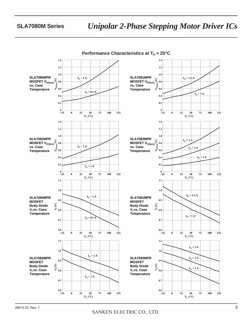
Performance Characteristics at TA = 25°C1.4
1.2
1.0
0.8
0.6
0.4
0.2
0–25 0 25 50 75 100 125
V DS(
on) (
V)SLA7080MPR
MOSFET VDS(on)vs. CaseTemperature
TC (°C)
1.4
1.2
1.0
0.8
0.6
0.4
0.2
0–25 0 25 50 75 100 125
V DS(
on) (
V)SLA7082MPR
MOSFET VDS(on)vs. CaseTemperature
TC (°C)
1.1
1.0
0.9
0.8
0.7
0.6–25 0 25 50 75 100 125
V f (V
)
SLA7080MPRMOSFET Body DiodeVf vs. CaseTemperature
TC (°C)
1.1
1.0
0.9
0.8
0.7
0.6–25 0 25 50 75 100 125
V f (V
)
SLA7081MPRMOSFET Body DiodeVf vs. CaseTemperature
TC (°C)
1.1
1.0
0.9
0.8
0.7
0.6–25 0 25 50 75 100 125
V f (V
)
SLA7082MPRMOSFET Body DiodeVf vs. CaseTemperature
TC (°C)
1.1
1.0
0.9
0.8
0.7
0.6–25 0 25 50 75 100 125
V f (V
)
SLA7083MPRMOSFET Body DiodeVf vs. CaseTemperature
TC (°C)
1.4
1.2
1.0
0.8
0.6
0.4
0.2
0–25 0 25 50 75 100 125
V DS(
on) (
V)SLA7081MPR
MOSFET VDS(on)vs. CaseTemperature
TC (°C)
1.4
1.2
1.0
0.8
0.6
0.4
0.2
0–25 0 25 50 75 100 125
V DS(
on) (
V)SLA7083MPR
MOSFET VDS(on)vs. CaseTemperature
TC (°C)
IO = 0.5 A
IO = 1 A
IO = 1 A
IO = 1.5 A
IO = 1 A
IO = 2 A IO = 2 A
IO = 1 A
IO = 3 A
IO = 0.5 A
IO = 1 A
IO = 1 A
IO = 1.5 A
IO = 1 A
IO = 2 A
IO = 3 A
IO = 2 A
IO = 1 A

6SANKEN ELECTRIC CO., LTD.
28610.23, Rev. 1
Unipolar 2-Phase Stepping Motor Driver ICsSLA7080M Series
Logic BlockThis circuit block is integrated on the Control IC (MIC). It oper-ates by the logic power supply, VDD , and propagates signals to each circuit block in accordance with the logic input signals.
Regulator CircuitThis circuit block is integrated on the Control IC (MIC). The integrated regulator circuit is used in driving the output MOSFET gates and in powering other internal linear circuits.
Dual Phase Output ControlThe SLA7080M series allows dual phase operation based on external input to the INx pins. The phase-switching logic is shown in the following table:
Phase A [B]
INA [INB] I N A [ I N B ] OUTA [OUTB]* O U T A [O U T B ]*
Low Low OFF OFF
High Low ON OFF
Low High OFF ON
High High OFF OFF
*OUT indicates power MOSFET drain state (does not indicate PWM operation)
PWM ControlThis circuit block is integrated on the Control IC (MIC). This is the main circuit block for pulse width modulated (PWM) control of self-excitation and external excitation for motor driving. An illustration of PWM behavior is shown in figure 1.
PWM control mode is set by the SYNC pin. Set SYNC to logic high for synchronous PWM, and set it to logic low for asynchro-nous PWM.
PWM Off-Time, toff, (for self-excitation), minimum off-time (for external excitation), and PWM Minimum On-Time (blanking time), ton(min), are clocked by means of the built-in oscillator.
The length of toff is fixed internally. Like in the SLA7070M series, the SLA7080M series has a power-saving function that reduces power consumption during toff. This function recirculates electromotive force that is stored in the motor coil while the power MOSFETs are turned on.
The time interval during which the output MOSFETs are on is ton. The minimum duration for the PWM Minimum On-time, ton(min) , is effectively the blanking time selected, even if the application attempts to shorten ton in order to limit current. The minimum coil current is at ton(min), so when the coil current is limited at power-down or other events, it can be no shorter than the blanking time.
Blanking TimeThe blanking time function is provided to limit current in order to suppress ringing immediately after PWM turns on, and to improve current control tracking. Blanking time in effect deter-mines PWM Minimum On-Time, ton(min). The length of the blank-ing time is selected by the B_SEL pin. Set B_SEL to logic high for 3.2 μs blanking time, and set it to logic low for 5.2 μs.
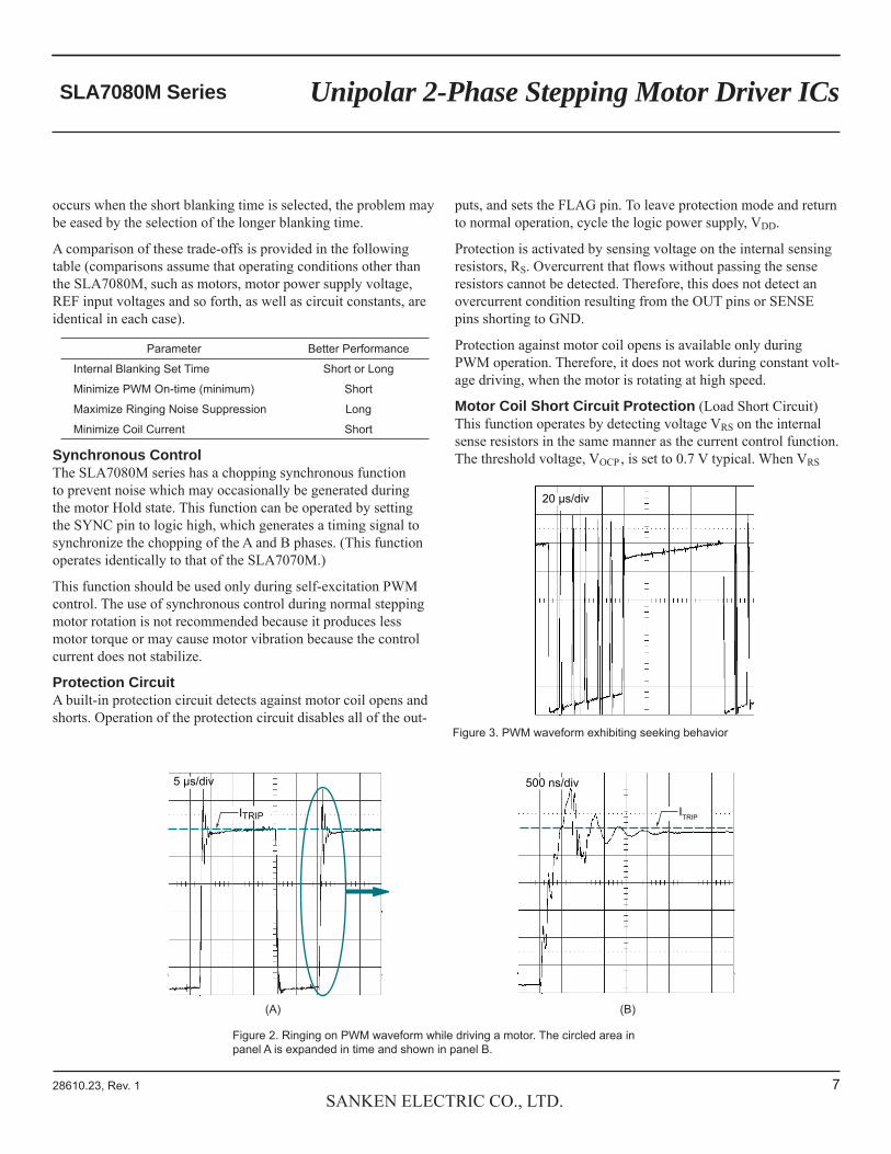
Some ringing is generated for a few microseconds after PWM switching (see figure 2). Ringing can result from various causes, such as capacitance between motor cells, or inappropriate motor wiring. To suppress this behavior, the blanking time selection sets a minimum time interval during which current detection signals from the current sense comparators are ignored after a PWM switch-on.
Current control (tracking) in the SLA7080M series is regulated by comparing the detection voltage on the sense resistor, VRS , with the reference voltage, VREF. If the ringing noise causes VRS to exceed VTRIP , the comparator is activated and PWM turns off.
Current control performance at shorter PWM waveforms can be improved by shortening the blanking time, but this decreases the effectiveness of ringing suppression, resulting in the seek-ing behavior shown in figure 3.) To solve this problem, the SLA7080M series is designed to allow dynamic selection of blanking time duration. In the event that the seeking behavior
Functional Description
Figure 1. PWM waveform on SLA7080M sense resistor, RS ; toff is fixed and the blanking time, toff(min) , is dynamically selectable.
0
VOUT
ton(min)
ITRIP
One PWM Cycle
ton toff
Phase A [B]
A [ B ]
A [ B ]
7SANKEN ELECTRIC CO., LTD.
28610.23, Rev. 1
Unipolar 2-Phase Stepping Motor Driver ICsSLA7080M Series
occurs when the short blanking time is selected, the problem may be eased by the selection of the longer blanking time.
A comparison of these trade-offs is provided in the following table (comparisons assume that operating conditions other than the SLA7080M, such as motors, motor power supply voltage, REF input voltages and so forth, as well as circuit constants, are identical in each case).
Parameter Better Performance
Internal Blanking Set Time Short or Long
Minimize PWM On-time (minimum) Short
Maximize Ringing Noise Suppression Long
Minimize Coil Current Short
Synchronous Control The SLA7080M series has a chopping synchronous function to prevent noise which may occasionally be generated during the motor Hold state. This function can be operated by setting the SYNC pin to logic high, which generates a timing signal to synchronize the chopping of the A and B phases. (This function operates identically to that of the SLA7070M.)
This function should be used only during self-excitation PWM control. The use of synchronous control during normal stepping motor rotation is not recommended because it produces less motor torque or may cause motor vibration because the control current does not stabilize.
Protection CircuitA built-in protection circuit detects against motor coil opens and shorts. Operation of the protection circuit disables all of the out-
puts, and sets the FLAG pin. To leave protection mode and return to normal operation, cycle the logic power supply, VDD.
Protection is activated by sensing voltage on the internal sensing resistors, RS. Overcurrent that flows without passing the sense resistors cannot be detected. Therefore, this does not detect an overcurrent condition resulting from the OUT pins or SENSE pins shorting to GND.
Protection against motor coil opens is available only during PWM operation. Therefore, it does not work during constant volt-age driving, when the motor is rotating at high speed.
Motor Coil Short Circuit Protection (Load Short Circuit) This function operates by detecting voltage VRS on the internal sense resistors in the same manner as the current control function. The threshold voltage, VOCP , is set to 0.7 V typical. When VRS
ITRIP
5 μs/div
ITRIP
500 ns/div
20 μs/div
Figure 3. PWM waveform exhibiting seeking behavior
Figure 2. Ringing on PWM waveform while driving a motor. The circled area in panel A is expanded in time and shown in panel B.
(A) (B)
8SANKEN ELECTRIC CO., LTD.
28610.23, Rev. 1
Unipolar 2-Phase Stepping Motor Driver ICsSLA7080M Series
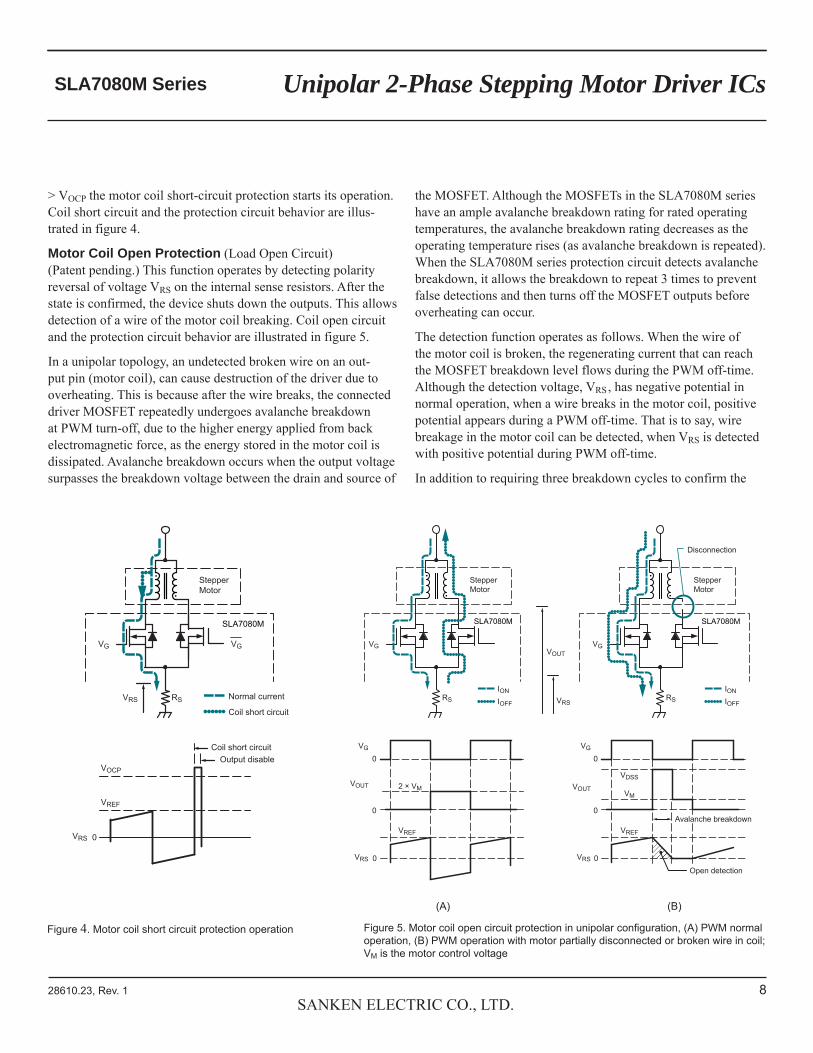
> VOCP the motor coil short-circuit protection starts its operation. Coil short circuit and the protection circuit behavior are illus-trated in figure 4.
Motor Coil Open Protection (Load Open Circuit) (Patent pending.) This function operates by detecting polarity reversal of voltage VRS on the internal sense resistors. After the state is confirmed, the device shuts down the outputs. This allows detection of a wire of the motor coil breaking. Coil open circuit and the protection circuit behavior are illustrated in figure 5.
In a unipolar topology, an undetected broken wire on an out-put pin (motor coil), can cause destruction of the driver due to overheating. This is because after the wire breaks, the connected driver MOSFET repeatedly undergoes avalanche breakdown at PWM turn-off, due to the higher energy applied from back electromagnetic force, as the energy stored in the motor coil is dissipated. Avalanche breakdown occurs when the output voltage surpasses the breakdown voltage between the drain and source of
the MOSFET. Although the MOSFETs in the SLA7080M series have an ample avalanche breakdown rating for rated operating temperatures, the avalanche breakdown rating decreases as the operating temperature rises (as avalanche breakdown is repeated). When the SLA7080M series protection circuit detects avalanche breakdown, it allows the breakdown to repeat 3 times to prevent false detections and then turns off the MOSFET outputs before overheating can occur.
The detection function operates as follows. When the wire of the motor coil is broken, the regenerating current that can reach the MOSFET breakdown level flows during the PWM off-time. Although the detection voltage, VRS , has negative potential in normal operation, when a wire breaks in the motor coil, positive potential appears during a PWM off-time. That is to say, wire breakage in the motor coil can be detected, when VRS is detected with positive potential during PWM off-time.
In addition to requiring three breakdown cycles to confirm the
Figure 4. Motor coil short circuit protection operation Figure 5. Motor coil open circuit protection in unipolar configuration, (A) PWM normal operation, (B) PWM operation with motor partially disconnected or broken wire in coil; VM is the motor control voltage
SLA7080M
0
VREF
VOCP
Coil short circuit
VG VG
StepperMotor
Normal currentVRS RS
VRS
Output disable
Coil short circuit
SLA7080M
0
VREF
0
0
VG
VOUT VOUT VM2 × VM
VDSS
VG
StepperMotor
IOFF
ION
VOUT
VRSRS
VRS
IOFF
ION
SLA7080M
0
VREF
Avalanche breakdown
0
0
VG
VG
StepperMotor
Disconnection
RS
VRS
Open detection
(A) (B)

9SANKEN ELECTRIC CO., LTD.
28610.23, Rev. 1
Unipolar 2-Phase Stepping Motor Driver ICsSLA7080M Series
open circuit condition, the SLA7080M protection function also provides a fixed delay, topp, before the device shuts down the outputs. This is to avoid false detections based on ringing after PWM turn-off. Referring to figure 6, if the breakdown confirma-tion interval (3 breakdown cycles) plus ringing effects are shorter than topp , the protection circuit functions correctly. However, if ringing causes the total period to exceed topp, false detections can occur. If this is the case, check the motor and wiring layout to reduce ringing. Variation among device variants and applications should be taken into consideration. One possible solution is the addition of a capacitor between the OUTx and GND pins, which could damp the ringing sufficiently to allow continuation of nor-mal operation when there is no actual avalanche breakdown.
Synchronous RectificationA dead time, approximately 0.5 μs, is set to prevent simultane-ous turn-on of the MOSFETs at switching during synchronous rectification. During the dead time, the regenerating current flows through the body diode on each MOSFET chip, as shown in figure 7.
Power SupplyThere is no restriction on the on/off sequencing of the main power supply, VBB, and the logic supply, VDD. Because the SLA7080M series has a structure that separates the Control IC (MIC) with the power MOSFET of the output stage, the motor power supply and the main power supply are electrically separated. Therefore, it is possible to drive the device by using different voltages for motor power supply and main power supply. Note that the power sup-plies have different voltage ranges.
Figure 6. Alternative topp scenarios: (A) no ringing, breakdown confirmed after three cycles, (B) ringing plus three cycles is less than topp with no effect on operations, and (C) ringing is greater than topp generates false detections of breakdowns
tOPP
tCONFIRM tCONFIRM tCONFIRM
tOPP tOPP
VOUT
VDSS
(A) (B) (C)
Figure 7. Synchronous rectification operation
SLA7080M
0
VREF
0
0
VG
VG
PWM On
tDEAD tDEAD
PWM OnPWM Off
VG VG
StepperMotor
Back EMF duringdead time
Normal currentVRS RS
ION IOFF
VRS
10SANKEN ELECTRIC CO., LTD.
28610.23, Rev. 1
Unipolar 2-Phase Stepping Motor Driver ICsSLA7080M Series
Application Information
INA, I N A , INB, I N B , B_SEL, and SYNC pinsThese inputs operate with CMOS input. The default state is high impedance, and they must be driven to logic high or logic low. When these logic input pins are used, they should be pulled down to the ground side using a 1 to 10 kΩ resistor. Any of these pins that are not used must either be pulled up to the VDD side or be pulled down to the ground side.
If they are left open, malfunction or permanent damage to the product may result. For example, in case the signal from the microcomputer has high impedance, a pull-down or pull-up resis-tor should be provided. In particular, when an INx pin is in high impedance during operation, abnormal oscillation of the output may be caused and in the worst case, this will result in permanent damage to the MOSFETs.
A low pass filter (LPF) is provided on each the logic input pin. These improve noise filtering.
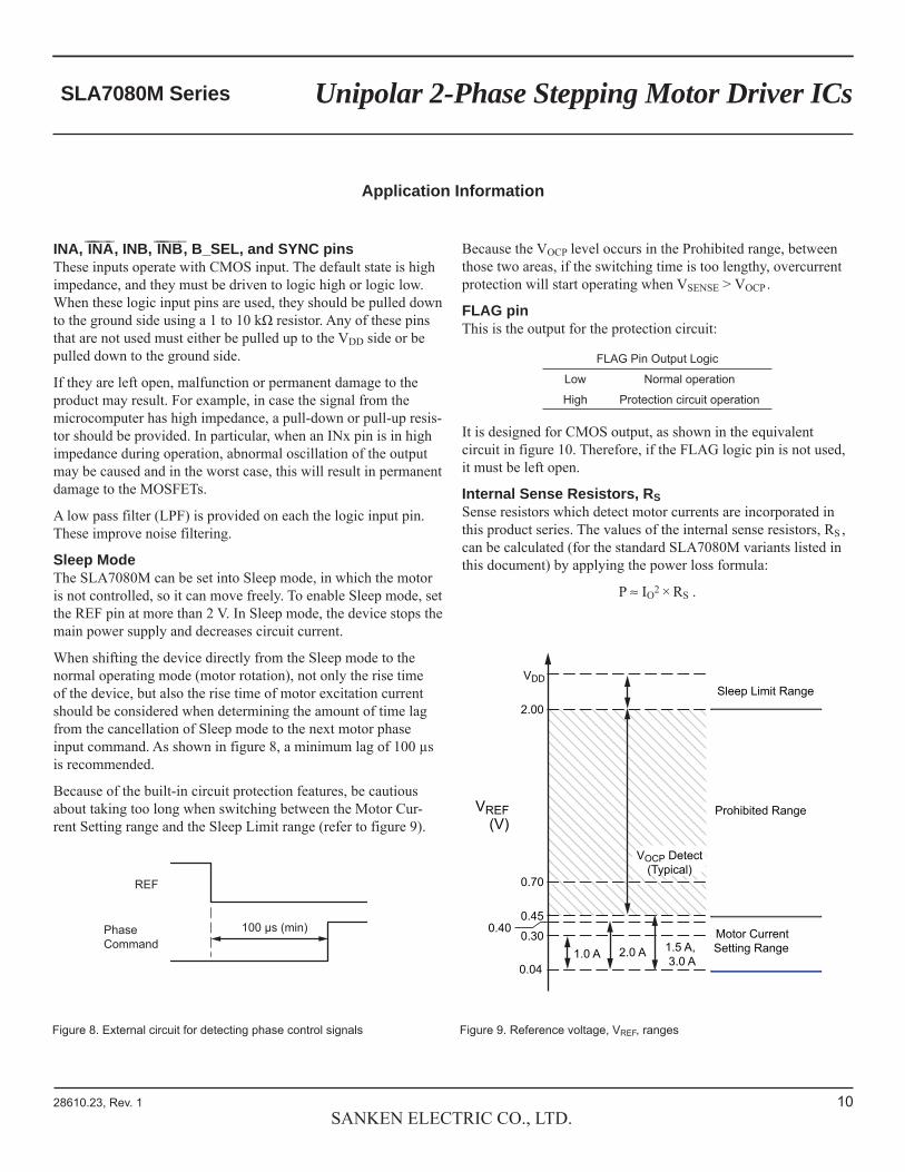
Sleep Mode The SLA7080M can be set into Sleep mode, in which the motor is not controlled, so it can move freely. To enable Sleep mode, set the REF pin at more than 2 V. In Sleep mode, the device stops the main power supply and decreases circuit current.
When shifting the device directly from the Sleep mode to the normal operating mode (motor rotation), not only the rise time of the device, but also the rise time of motor excitation current should be considered when determining the amount of time lag from the cancellation of Sleep mode to the next motor phase input command. As shown in figure 8, a minimum lag of 100 μs is recommended.
Because of the built-in circuit protection features, be cautious about taking too long when switching between the Motor Cur-rent Setting range and the Sleep Limit range (refer to figure 9).
Because the VOCP level occurs in the Prohibited range, between those two areas, if the switching time is too lengthy, overcurrent protection will start operating when VSENSE > VOCP .
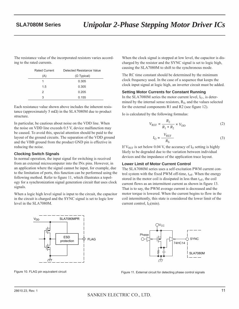
FLAG pinThis is the output for the protection circuit:
FLAG Pin Output Logic
Low Normal operation
High Protection circuit operation
It is designed for CMOS output, as shown in the equivalent circuit in figure 10. Therefore, if the FLAG logic pin is not used, it must be left open.
Internal Sense Resistors, RSSense resistors which detect motor currents are incorporated in this product series. The values of the internal sense resistors, RS , can be calculated (for the standard SLA7080M variants listed in this document) by applying the power loss formula:
P ≈ IO2 × RS .
Figure 9. Reference voltage, VREF, ranges
VREF(V)
2.00Sleep Limit Range
Motor CurrentSetting Range
VDD
VOCP Detect(Typical)
1.5 A, 3.0 A
2.0 A1.0 A
Prohibited Range
0.70
0.45
0.30
0.04
0.40
Figure 8. External circuit for detecting phase control signals
100 μs (min)
REF
PhaseCommand
11SANKEN ELECTRIC CO., LTD.
28610.23, Rev. 1
Unipolar 2-Phase Stepping Motor Driver ICsSLA7080M Series
The resistance value of the incorporated resistors varies accord-ing to the rated currents.
Rated Current Detected Resistance Value
(A) (Ω Typical)
1 0.305
1.5 0.305
2 0.205
3 0.155
Each resistance value shown above includes the inherent resis-tance (approximately 5 mΩ) in the SLA7080M due to product structure.
In particular, be cautious about noise on the VDD line. When the noise on VDD line exceeds 0.5 V, device malfunction may be caused. To avoid this, special attention should be paid to the layout of the ground circuits. The separation of the VDD ground and the VBB ground from the product GND pin is effective in reducing the noise.
Clocking Switch SignalsIn normal operation, the input signal for switching is received from an external microcomputer into the INx pins. However, in an application where the signal cannot be input, for example, due to the limitation of ports, this function can be performed using the following method. Refer to figure 11, which illustrates a topol-ogy for a synchronization signal generation circuit that uses clock signals.
When a logic high level signal is input to the circuit, the capacitor in the circuit is charged and the SYNC signal is set to logic low level in the SLA7080M.
When the clock signal is stopped at low level, the capacitor is dis-charged by the resistor and the SYNC signal is set to logic high, causing the SLA7080M to shift to the synchronous mode.
The RC time constant should be determined by the minimum clock frequency used. In the case of a sequence that keeps the clock input signal at logic high, an inverter circuit must be added.
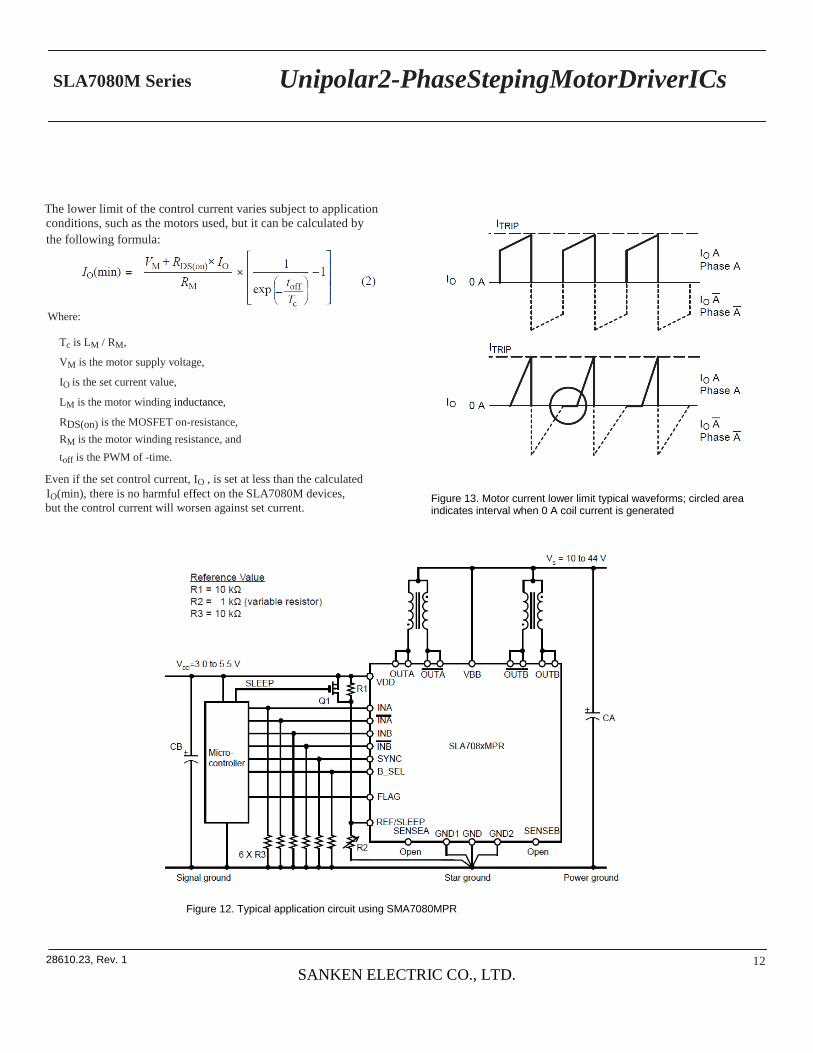
Setting Motor Currents for Constant RunningIn the SLA7080M series the motor current level, IO , is deter-mined by the internal sense resistors, RS, and the values selected for the external components R1 and R2 (see figure 12).
Io is calculated by the following formulas:
R2
R1 + R2 × VDDVREF = (2)
VREF
RSIO = (3)
If VREF is set below 0.04 V, the accuracy of IO setting is highly likely to be degraded due to the variation between individual devices and the impedance of the application trace layout.
Lower Limit of Motor Current ControlThe SLA7080M series uses a self-excitation PWM current con-trol system with the fixed PWM off-time, toff . When the energy stored in the motor coil is dissipated in less than toff , the coil current flows as an intermittent current as shown in figure 13. That is to say, the PWM average current is decreased and the motor torque is lowered. When the current begins to flow in the coil intermittently, this state is considered the lower limit of the current control, IO(min).
Figure 10. FLAG pin equivalent circuit Figure 11. External circuit for detecting phase control signals
FLAG
VDD SLA7080MPR
ESD protection
SLA7080M
Phase
VCC
74HC14SYNC
12
SLA7080M Series Unipolar2-PhaseStepingMotorDriverICs
The lower limit of the control current varies subject to application
conditions, such as the motors used, but it can be calculated by
the following formula:
Where:
Tc is LM / RM,
VM is the motor supply voltage,
IO is the set current value,
LM is the motor winding inductance,
RDS(on) is the MOSFET on-resistance,
RM is the motor winding resistance, and
toff is the PWM of -time.
Even if the set control current, IO , is set at less than the calculated
IO(min), there is no harmful effect on the SLA7080M devices,
but the control current will worsen against set current.
Figure 13. Motor current lower limit typical waveforms; circled area indicates interval when 0 A coil current is generated
Figure 12. Typical application circuit using SMA7080MPR
28610.23, Rev. 1
SANKEN ELECTRIC CO., LTD.
13SANKEN ELECTRIC CO., LTD.
28610.23, Rev. 1
Unipolar 2-Phase Stepping Motor Driver ICsSLA7080M Series
Verification of Avalanche EnergyDue to the unipolar topology of the SLA7080M series, a surge voltage (ringing) that exceeds the MOSFET breakdown volt-age might be applied to the device. In anticipation of this surge voltage, the SLA7080M series uses MOSFETs having sufficient avalanche resistance to withstand such surge voltages. Therefore, even if a surge voltage occurs, users will be able to use the device without any problem.
However, if the motor wiring harness is long or the SLA7080M is used at greater than the rated current or voltage, an avalanche energy beyond our design expectations may be applied to the device. Thus, users must test the avalanche energy applied to the device under actual application conditions.
The following procedure can be used to check the avalanche energy in an actual application. The following typical values
result from testing (refer to figure 15):
VDS(av) = 140 VID = 1 At = 0.5 μs
The avalanche energy, EAV, is obtained by substituting values into the following formula:
VDS(av)× 0.5 × ID × tEAV ≈140 V × 0.5 × 1 A × 0.5 × 10-6=0.035 (mJ)=
(2)
The EAV thus calculated is compared with the graph shown in figure 15 to confirm that the EAV is within the safe operating area of the avalanche breakdown voltage of the MOSFETs.
Thermal DesignThe SLA7080M series incorporates a thermal protection func-tion that shuts down all outputs when the Control IC tempera-ture exceeds TTSD. However, a comprehensive overtemperature protection function is not provided because the Control IC chip is separate from the MOSFET chips, the power elements which are the primary sources of heat. It would be unable to respond to sudden temperature changes in the MOSFETs because of delays in diffusion of the heat.
Therefore, sufficient thermal evaluation should be performed with the actual application, so that the junction temperature, TJ , does not exceed the absolute maximum rating (150°C). Experimentation is required because it is not practical to calcu-late a realistic power dissipation value, which involves variable parameters such as time constants and excitation modes during actual operation of motors, input frequencies and sequences, and so forth.
Figure 14. Test points and waveform for testing avalanche energy of an application
Figure 15. Avalanche breakdown voltages for repeated cycles
SLA7080M
t
VDS(av)
ID
StepperMotor
VDS(av)
ID
RS
00 25 50 75 100 125 150
4
8
12
16
20
TC (°C)
E AV (m
J)
SLA7083MPR
SLA7082MPR
SLA7080MPR
SLA7081MPR

14SANKEN ELECTRIC CO., LTD.
28610.23, Rev. 1
Unipolar 2-Phase Stepping Motor Driver ICsSLA7080M Series
Given this situation, for initial design estimates, power dissipa-tion should be calculated by approximation, using worst-case conditions, at 2-phase excitation:
PD = IO 2 × ( RDS(on) + RS ) × 2 , (6)
where:
PD is the power dissipation of the SLA7080M,IO is the Output Current,RDS(on) is the on-resistance of the MOSFETs, andRS is the Sense Resistor Resistance.
Based on the power dissipation of the product thus calculated, the junction temperature of the product is estimated by using the temperature rise curves of figure 16.
Unless the temperature exceeds 150°C under the worst condi-tions (the maximum values of ambient operating temperature), there will be no problem, but final judgment should be made by measuring the device temperature during the actual operation and then verifying power dissipation and junction temperature in accordance with figure 16.
When the device is used with a heatsink, the thermal resis-tance, RθJA , of the device changes (as do the parameters used in calculating ΔTJA ). This value is calculated from the following
formula: RθJA ≈ RθCA + RθHS
= ( RθJA – RθCA ) + RθHS , (7)
where RθHS is the thermal resistance of the heatsink.
To estimate the junction temperature rise, ΔTJ , from the device temperature measured in the actual operating application, ΔTCA , the following procedure should be followed:
1. The temperature rise of the product, ΔTCA , is measured on pin 12, where it enters the case.
2. From the temperature rise thus obtained, the power dissipation, PD , and the junction temperature, TJ , are estimated using figure 16.
3. Calculate the relationship between ΔTCA and the junction temperature rise, ΔTJ , using the following formula:
ΔTJ ≈ ΔTJ C + PD × RθJC . (8)
Note that this thermal design information is provided for pre-liminary design estimations only. Users should verify the heat generation of the product in the actual operation, by measuring the case temperature, TC, and comparing it to the Recommended Operating Conditions table values.
Figure 16. Power dissipation estimate for junction-to-ambient and case-to-ambient temperature change
0
25
50
75
100
125
150
0 0.5 1.0 1.5 2.0 2.5 3.0 3.5 4.0 4.5 5.0
Cha
nge
in T
empe
ratu
re, ∆
T (°
C)
Allowable Power Dissipation, PD (W)
∆TJA = 26.6 × PD
∆TCA = 21.3 × PD
15SANKEN ELECTRIC CO., LTD.
28610.23, Rev. 1
Unipolar 2-Phase Stepping Motor Driver ICsSLA7080M Series
1 3 5 7 9 11 13 15 17 19 21 23
2 4 6 8 10 12 14 16 18 20 22Pad Side
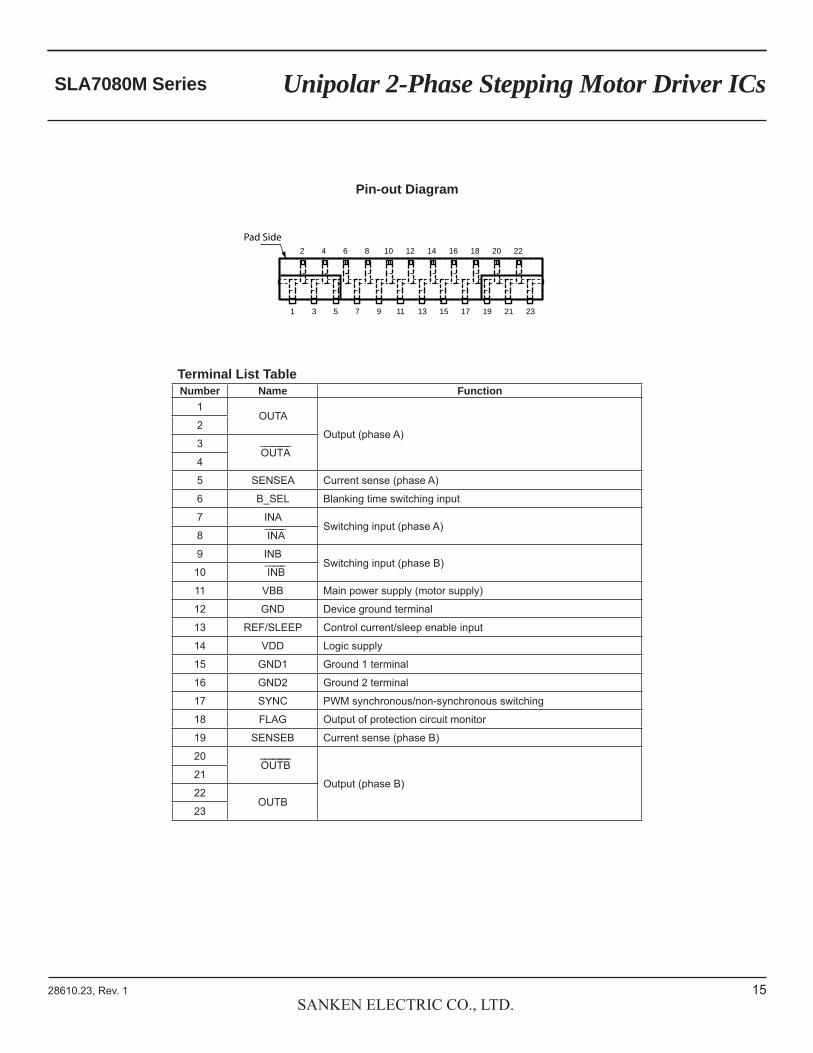
Pin-out Diagram
Terminal List TableNumber Name Function
1OUTA
Output (phase A)2
3 O U T A
4
5 SENSEA Current sense (phase A)
6 B_SEL Blanking time switching input
7 INASwitching input (phase A)
8 I N A
9 INBSwitching input (phase B)
10 I N B
11 VBB Main power supply (motor supply)
12 GND Device ground terminal
13 REF/SLEEP Control current/sleep enable input
14 VDD Logic supply
15 GND1 Ground 1 terminal
16 GND2 Ground 2 terminal
17 SYNC PWM synchronous/non-synchronous switching
18 FLAG Output of protection circuit monitor
19 SENSEB Current sense (phase B)
20 O U T B
Output (phase B)21
22OUTB
23

16SANKEN ELECTRIC CO., LTD.
28610.23, Rev. 1
Unipolar 2-Phase Stepping Motor Driver ICsSLA7080M Series
Terminal core material: CuTerminal plating: Ni, with Pb-free solder coatingRecommended attachment: Solder dip (Sn-Ag-Cu)
Dimensions in millimeters
Branding codes (exact appearance at manufacturer discretion):1st line, type: SLA708xMR2nd line, protection: P 3rd line, lot: YMDD Where: Y is the last digit of the year of manufacture M is the month (1 to 9, O, N, D) DD is the date
Branding Area
Exposed heatsink pad
1.27 ±0.5
0.6
0.65 +0.2– 0.1
9.3 +0.1– 0.5 0.55 +0.2
– 0.1
16.4 ±0.2
24.4 ±0.2
Ø3.2 ±0.15
31 ±0.2
Gate protrusion
Gate protrusion
9.9 ±0.2
12.9 ±0.2
16 ±0.2
A
A
BMeasured at pin tips
To case top
1 3 5 7 9 11 13 15 17 19 21 23
2 4 6 8 10 12 14 16 18 20 22
1.7 ±0.1
4.8 ±0.2
R1REF
4.3REF 4.5 ±0.7
5 ±0.5
2.45 ±0.2BSC
View ADeflection at pin bend
0.7 MAX
B
Ø3.2 ±0.15
31.3 ±0.2
View A
Package Outline DrawingDual rows, 23 alternating pins; vertical case mounting; pin #1 opposite pad side
Leadframe plating Pb-free. Device composition complies with the RoHS directive.
17SANKEN ELECTRIC CO., LTD.
28610.23, Rev. 1
Unipolar 2-Phase Stepping Motor Driver ICsSLA7080M Series
Because reliability can be affected adversely by improper storage environments and handling methods, please observe the following cautions.Cautions for Storage• Ensure that storage conditions comply with the standard
temperature (5°C to 35°C) and the standard relative humidity (around 40 to 75%); avoid storage locations that experience extreme changes in temperature or humidity.
• Avoid locations where dust or harmful gases are present and avoid direct sunlight.
• Reinspect for rust on leads and solderability of products that have been stored for a long time.
Cautions for Testing and Handling When tests are carried out during inspection testing and other
standard test periods, protect the products from power surges from the testing device, shorts between adjacent products, and shorts to the heatsink.
Remarks About Using Silicone Grease with a Heatsink• When silicone grease is used in mounting this product to a
heatsink, it shall be applied evenly and thinly. If more silicone grease than required is applied, it may produce stress.
• Volatile-type silicone greases may permeate the product and produce cracks after long periods of time, resulting in reduced heat radiation effect, and possibly shortening the lifetime of the product.
• Our recommended silicone greases for heat radiation purposes, which will not cause any adverse effect on the product life, are indicated below:
Type SuppliersG746 Shin-Etsu Chemical Co., Ltd.
YG6260 Momentive Performance Materials Inc.
SC102 Dow Corning Toray Co., Ltd.
Heatsink Mounting MethodTorque When Tightening Mounting Screws. The recommended tightening
torque for this product package type is: 58.8 to 78.4 N•cm (6.0 to 8.0 kgf•cm).
Soldering• When soldering the products, please be sure to minimize the
working time, within the following limits: 260±5°C 10 s 380±5°C 5 s• Soldering iron should be at a distance of at least 1.5 mm from the
body of the productsElectrostatic Discharge• When handling the products, operator must be grounded.
Grounded wrist straps worn should have at least 1 MΩ of resistance to ground to prevent shock hazard.
• Workbenches where the products are handled should be grounded and be provided with conductive table and floor mats.
• When using measuring equipment such as a curve tracer, the equipment should be grounded.
• When soldering the products, the head of soldering irons or the solder bath must be grounded in other to prevent leak voltages generated by them from being applied to the products.
• The products should always be stored and transported in our shipping containers or conductive containers, or be wrapped in aluminum foil.

18SANKEN ELECTRIC CO., LTD.
28610.23, Rev. 1
Unipolar 2-Phase Stepping Motor Driver ICsSLA7080M Series
• The contents in this document are subject to changes, for improvement and other purposes, without notice. Make sure that this is the latest revision of the document before use.
• Application and operation examples described in this document are quoted for the sole purpose of reference for the use of the prod-ucts herein and Sanken can assume no responsibility for any infringement of industrial property rights, intellectual property rights or any other rights of Sanken or any third party which may result from its use.
• Although Sanken undertakes to enhance the quality and reliability of its products, the occurrence of failure and defect of semicon-ductor products at a certain rate is inevitable. Users of Sanken products are requested to take, at their own risk, preventative measures including safety design of the equipment or systems against any possible injury, death, fires or damages to the society due to device failure or malfunction.
• Sanken products listed in this document are designed and intended for the use as components in general purpose electronic equip-ment or apparatus (home appliances, office equipment, telecommunication equipment, measuring equipment, etc.).
When considering the use of Sanken products in the applications where higher reliability is required (transportation equipment and its control systems, traffic signal control systems or equipment, fire/crime alarm systems, various safety devices, etc.), and whenever long life expectancy is required even in general purpose electronic equipment or apparatus, please contact your nearest Sanken sales representative to discuss, prior to the use of the products herein.
The use of Sanken products without the written consent of Sanken in the applications where extremely high reliability is required (aerospace equipment, nuclear power control systems, life support systems, etc.) is strictly prohibited.
• In the case that you use Sanken products or design your products by using Sanken products, the reliability largely depends on the degree of derating to be made to the rated values. Derating may be interpreted as a case that an operation range is set by derating the load from each rated value or surge voltage or noise is considered for derating in order to assure or improve the reliability. In general, derating factors include electric stresses such as electric voltage, electric current, electric power etc., environmental stresses such as ambient temperature, humidity etc. and thermal stress caused due to self-heating of semiconductor products. For these stresses, instantaneous values, maximum values and minimum values must be taken into consideration.
In addition, it should be noted that since power devices or IC's including power devices have large self-heating value, the degree of derating of junction temperature affects the reliability significantly.
• When using the products specified herein by either (i) combining other products or materials therewith or (ii) physically, chemically or otherwise processing or treating the products, please duly consider all possible risks that may result from all such uses in advance and proceed therewith at your own responsibility.
• Anti radioactive ray design is not considered for the products listed herein.• Sanken assumes no responsibility for any troubles, such as dropping products caused during transportation out of Sanken's distribu-
tion network.• The contents in this document must not be transcribed or copied without Sanken's written consent.