nano-accuracy surface figure metrology of precision optics
TRANSCRIPT

4
Nano-Accuracy Surface Figure Metrology of Precision Optics
Shinan Qian and Peter Takacs Brookhaven National Laboratory
USA
1. Introduction
Precision optical surface figure measurement is the most important aspect for optical
systems development of telescopes, microscopes, cameras and imaging or focusing
systems. Any optical surface slope error or surface figure error departure from the
theoretical surface will produce beam deviations according to Snell’s law (law of
refraction) for transmission optics or to the law of reflection for mirrors. Beam deviations
can be easily calculated by use of ray tracing methods. The deviated beam will blur the
image quality, enlarge the focus point, degrade the accuracy of the wave-front, and harm
the performance of the optical system. To avoid such errors, surface figure must be
manufactured and measured precisely.
"If you can not measure it, you can not improve it." This famous quote, attributed to Sir
William Thomson, Lord Kelvin, describes exactly the dilemma faced by manufacturers of
precision optical surfaces. It is especially true in the fabrication of mirrors used at extreme
grazing incidence angles to focus x-rays in telescope and synchrotron applications. Mirrors
used in synchrotron beam lines in the 1970s and '80s suffered from excessive surface
roughness, generating excessive amounts of scattered light which reduced focal spot
intensity and produced spectral contamination in VUV monochromators. The diamond
stylus profilometers available at the time were ill-suited for measurements of surface
roughness on full-size optical components. The development of the non-contact
interferometric phase-measuring microscope early in the 1980's made surface roughness
measurements in the Angstrom range on full-sized mirrors possible, and improvements in
surface finishing techniques were quick to follow (Bhushan et al., 1985; Koliopoulos et al.,
1980; Wyant et al., 1984)
The traditional measurements of plane and spheres applied test plate as a reference to test
the surface with interferometric method in early years, which can reach /10 or better
accuracy. However, this is contact test, and they are difficult to achieve with low-coherence
sources prior to the development of the HeNe laser. See the excellent discussion of various
historic interferometers in Malacara's book Optical Shop Testing (Malacara, D., 1992). Later
the development of different kind interferometers and the application of interference laser
promise the non contact measurements. Computerized interferometer with the CCD sensor
application and rapid fringe analysis enhanced the measurement technology accuracy
www.intechopen.com

Modern Metrology Concerns 78
quickly. Computer generated holograph (CGH) method (Pruss, 2008) can replace the
troublesome preparation of test plates. In recent decades the development of the phase
measuring interferometer (PMI) becomes an excellent metrology method to promote the
interferometer accuracy and repeatability significantly, which has become a standard
procedure for the interferometers. The basic concept of the PMI is that one can calculate the
precise phase by acquiring several phase shifted frames of interferograms, each phase is
shifted by a certain amount. Measurement method accuracy of the PMI could be >1/1000
fringe comparing to previous fringe analysis accuracy of only 1/10 fringe. The advantages
of the PMI are the high accuracy can be obtained with low contrast fringes and is
independent of intensity variations across pupil. Measurement of /20 surfaces is no longer
a black art practiced by master opticians but is possible by ordinary shop technicians using
modern phase measuring interferometers. These PMI instruments are widely used in the
workshop and the research laboratory because of their ability to make non-contact
measurements over large areas with high precision.
The PMI has successfully resolved two major tasks for precise metrology of routine or research surfaces: a) measuring surface roughness with height resolution of less than 1
Angstrom; b) measuring larger 2D surface profiles with /1000 repeatability and improving the test accuracy. In a conventional phase-shifting laser interferometer, multiple frames of data are acquired in sequence, so there is enough time for vibration and turbulence to degrade the measurement results. Recently developed technology acquires all phase data simultaneously. This will be very useful for in situ precision testing in the workshop (Zecchino, M., 2008; ESDI, 2011)
However, in the case of using PMI, a reference mirror is always required as the measurement standard, which dominates the final possible measurement accuracy.
The metrology problem is more acute in the fabrication of aspheric optics. In recent decades, high technology developments of computer numerical control (CNC), diamond turning, magnetorheological finishing (MRF), ion polishing, and elastic emission machining (EEM) have removed many of the difficulties involved in the manufacture of aspherics and high accuracy conventional optics. These manufacturing techniques have enabled the fabrication of nano-radian and nanometer accuracy components required in various applications.
Several recently-developed metrology techniques extend the measurement capabilities of
conventional interferometers. Liu, et al., developed a sub-aperture technique for measuring
on-axis aspheres by combining annular regions measured with a Twyman-Green
interferometer (Liu et al., 1988). This technique works by adjusting the distance to the test
surface to match the wavefront curvature to the surface radius at each zonal region. Sub-
aperture stitching interferometry (SSI), developed by QED, enables the testing of larger
aperture optics with standard Fizeau reference optics, without the need for dedicated large
null optics, by automatically combining multiple overlapping sub-aperture measurements
to form a full-aperture measurement (Fleig et al., 2003; Murphy et al., 200; 2003). The QED
system simultaneously produces an error map of both the larger test surface and the smaller
reference surface, correcting for rigid body alignment in each sub-aperture and for reference
surface errors. Measurement error repeatability has been demonstrated to be 2 nm rms.
Relative angle determinable stitching interferometry (RADSI) was also developed by the
Osaka University group to measure steeply curved X-ray mirrors with nanometer accuracy
www.intechopen.com

Nano-Accuracy Surface Figure Metrology of Precision Optics 79
(Mimura et al., 2005; Yamauchi et al., 2003; Yumoto et al., 2010). In this method, the relative
angles between overlapping sub-apertures are determined simultaneously with one
interferometer while acquiring the sub-aperture profiles with another. Because stitching
analysis eliminates certain systematic errors inherent in large aperture systems, the SSI
enhances the accuracy of measurements. However, stitching methods can accumulate small
systematic interferometer errors that limit very high accuracy. Hence, the measurement
accuracy of a full-size surface needs to be calibrated precisely.
2. New demands on nano-accuracy metrology
Nanometer and nanoradian accuracy (for simplicity we use “nano” for nanometer or nano-radian or both) is required in many high technology areas: synchrotron radiation (SR) optics, extreme ultra-violet lithography (EUVL), cameras, telescopes, X-ray free electron lasers (XFEL), laser ignition facilities, freeform optics and so on.
2.1 Nano-accuracy requirement of synchrotron optics
Hard X-rays produced by synchrotron radiation (SR) sources are important tools for chemical, elemental, and structural analyses of matter at the nano- and atomic scale and for elucidating the molecular processes involved in biological functions at the cellular level. Scientists anticipate having one-nanometer probe spots for such research. Recently, construction started on ultra-bright SR sources with nano-focusing spots at the National Synchrotron Light Source II (NSLS II), Brookhaven National Laboratory (BNL) in the United States and at the Taiwan Photon Source (TPS) of the NSSRC. The NSLS II will allow researchers to create high-contrast X-ray images of matter at this resolution. To focus the bright, hard X-rays of a SR beam into a 1nm spot, beam lines must incorporate a series of precise optical elements. One of the most promising approaches to do so is the application of total reflection mirrors with their exceptional characteristics of broadband focusing, achromaticity, and high efficiency. Osaka University has focused hard x-rays to a spot size of approximately 7 nm using Kirkpatrick–Baez mirrors (K-B mirror) (Yamauchi et al., 2011). However, the mirror figure employed to focus a SR beam to a nanometer spot while preserving coherence requires nano-radian (nrad) accuracy. According to simple geometric-optics calculations, if the error in surface slope is 100 nrad, the beam will exhibit a lateral displacement of 4 nm at a 20mm focal distance; hence, it will greatly enlarge the 1nm spot.
Synchrotron radiation optics, operating at extreme grazing incidence angles on the order of a few milliradians, utilize surfaces consisting of planes, spheres, and aspheres including cylinders, toroids, paraboliods, and ellipsoids, up to 1.5 meters long. These lengthy cylinder-like aspheric surfaces normally have a long tangential radius of curvature, in the range from one hundred meters to several kilometers, with a sagittal radius of curvature that can be as short as a few centimeters. These surfaces are extremely difficult to measure with a traditional null interferometer, even with special computer-generated hologram (CGH) null lenses, or with an SSI. The new beam lines at the NSLS II will require many optical surfaces with 100 nrad slope error.
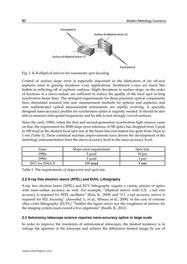
Fig. 1 is an example of SR optics, a K-B mirror set used for focusing X-ray beam to a nanometer spot. Two nano-accuracy elliptical cylinder mirrors are used to focus a beam to a single point in horizontal and vertical direction individually.
www.intechopen.com
Modern Metrology Concerns 80
Fig. 1. K-B elliptical mirrors for nanometer spot focusing
Control of surface slope error is especially important in the fabrication of far off-axis aspheres used in grazing incidence x-ray applications. Incoherent x-rays act much like bullets in reflecting off of aspheric surfaces. Slight deviations in surface slope, on the order of fractions of a micro-radian, are sufficient to reduce the quality of the focal spot in long synchrotron beam lines. The stringent requirements for these precision optical components have stimulated research into new measurement methods for spheres and aspheres, and new sophisticated optical measurement instruments are rapidly evolving. A specially designed nano-accuracy profiler for synchrotron optics is urgently needed. It should be also able to measure mid-spatial frequencies and be able to test strongly curved surfaces.
Since the early 1980s, when the first and second-generation synchrotron light sources came on-line, the requirement for RMS slope error tolerance of SR optics has dropped from 5 μrad to 100 nrad as the desired focal spot size at the beam line end-station has gone from 10µm to 1 nm (Table 1). These continual machine improvements have driven the development of the metrology instrumentation from the micro-accuracy level to the nano-accuracy level.
Years Slope error requirement Spot size
1980s 5 μrad 10 μm
1990s 1 μrad 1 μm
2011 for NSLS II 100 nrad 1 nm
Table 1. The requirements of slope error and spot size
2.2 X-ray free electron lasers (XFEL) and EUVL Lithography
X-ray free electron lasers (XFEL) and EUV lithography require a variety precise of optics with nano-radian accuracy as well. For example, “elliptical mirror with 0.21 μrad rms
accuracy is required for XFEL oscillator” (Kim, K., 2009) and ”0.1 μrad accuracy mirror is
required for FEL focusing” (Assoufid, L. et al.; Minura et al., 2008). In the case of extreme ultra violet lithography (EUVL) “Neither the figure errors nor the roughness of mirrors for the imaging system must exceed a few angstroms” (Soufli, R., 2011).
2.3 Astronomy telescope science requires nano-accuracy optics in large scale
In order to improve the resolution of astronomical telescopes, the desired tendency is to enlarge the aperture of the telescope and achieve the diffraction limited image by use of
www.intechopen.com

Nano-Accuracy Surface Figure Metrology of Precision Optics 81
perfect optics. This leads to the application of optics with nano-accuracy. This is the new challenge to manufacturing and metrology. Following quoted contents is the clear examples for describing these demands.
“The NASA Science Missions Directorate seeks technology for nano-accuracy metrology on NASA SBIR AND STTR 2011 Program Solicitations. Following are some requirements for telescopes: “Metrology instruments should have 10 nm or better surface height resolution and span at least 3 orders of magnitude in lateral spatial frequency for Optics Manufacturing and Metrology of Telescope Optical Surfaces” and “In situ metrology systems that can measure optics and provide feedback to figuring/polishing instruments without removing the part from the spindle”. “NASA is preparing potential future space telescopes, which have very specific mirror technology needs. UV/optical telescopes require 1 to 3 meter class mirrors with < 5 nm rms surface figures. IR telescopes (such as SAFIR/CALISTO) require 2 to 3 to 8 meter class mirrors with cryo-deformations < 100 nm rms. X-ray telescopes (such as GenX) require 1 to 2 meter long grazing incidence segments with angular resolution < 5 arc-sec down to 0.1 arc-sec and surface micro-roughness < 0.5-nm rms.” (NASA NASA SBIR and STTR 2011 Program Solicitations)
2.4 Precision measurement requirements for large radius of curvature
In order to ensure similar performance for each laser line of National Ignition Facility (NIF), it is necessary to keep each surface radius of curvature identical. The interferometric method is generally used to measure the radius of curvature of a spherical optical surface. However, it is difficult to perform on surfaces with large radii exceeding a few meters with large aperture, because it requires the test part to be moved over a distance equal to its radius. It means the distance between the surface under test and the reference is very long so it increases the measurement uncertainty. The NIF developed a method, based on dual-focus zone plates to solve this problem (Wang, Q. et al., 2008). In contrast to the NIF, Chengdu Fine Optical Engineering Research Center in China had made the measurement of long radius of curvature on large aperture lens with pencil bean scanning LTP-MF (Ye & Yang, 2011) with very promised accuracy. The nano-accuracy measurement can increase the test accuracy of radii of curvature significantly.
3. Early developments in nano-accuracy metrology
3.1 Scanning profilers
Except for the PMI and SSI, various specialized optical metrology techniques have been developed over the years to measure this class of optics, based upon scanning profilers: the Random Devices slope scanner (DeCew et al., 1986), the Zeiss M400 CMM in Germany (Becker et al., 1987), various instruments at the National Physical Laboratory in the UK (Ennos et al., 1982; Stedman et al., 1979), and the fringe scanner developed by Hughes Aircraft for the measurement of the AXAF (Chandra) x-ray telescope optics (Sarnik & Glenn, 1987) are examples of scanning profilers. These instruments employ various kinds of metrology methods, contact stylus and non-contact optical, developed to suit the particular metrology problem at hand. The Stedman-Stanley profiler (Stedman et al., 1979) and the Heynacher profilers (Heynacher & Reinhardt, 1979) were stylus instruments that made contact with the surface under test. These instruments made it possible to assess the height of steep aspheric surfaces at the nanometer level in two dimensions. Nevertheless, they are contact measurements, and
www.intechopen.com
Modern Metrology Concerns 82
during the final testing of optics with delicate coatings applied, there is always the possibility of leaving a very slight mark on the reflecting surface. Non-contact profiling methods have superceded contact stylus methods in the production of most grazing incidence optics today. Profiling instruments based upon the pencil-beam interferometer (PBI) are now widely employed in the manufacture and testing of SR and x-ray telescope optics (von Bieren, 1983a; 1983b; Takacs et al., 1988; Takacs et al., 1989). The PBI has been shown to be quite versatile and ideally suited for the testing of large cylindrical aspheres with nano-accuracy.
3.2 Pencil beam scanning surface profiler development in past 25 years
Soon after the NSLS x-ray ring was commissioned in the early 1980's, it was realized that the quality of the focused beam was being compromised by the less-than-perfect figure of the mirrors. The normal-incidence surface figure measurement techniques available to manufacturers at the time were inadequate for characterizing the slope errors in the grazing incidence optics, slope errors that produced blurring of the focus by several times the expected source-size-limited spot size. Conventional interferometry was practically useless in attempting to extract useful surface error information from extremely foreshortened apertures seen at grazing incidence angles on the paraboloids, toroids and ellipsoids in beam line instruments, making it difficult for manufacturers to produce good quality optics. Null lenses did not (and still do not) exist to allow the use of Fizeau interferometers to easily measure simple cylinders for use at 3 mrad grazing incidence angles. With these limitations in mind, we sought to develop a versatile measuring instrument that did not require the use of null lenses and that could handle a wide variety of grazing incidence optics: long, flat mirrors; long-radius spheres; cylinders; toroids; ellipsoids and elliptical cylinders; and bent optics with radii of curvature in the range of kilometers down to tens of meters.
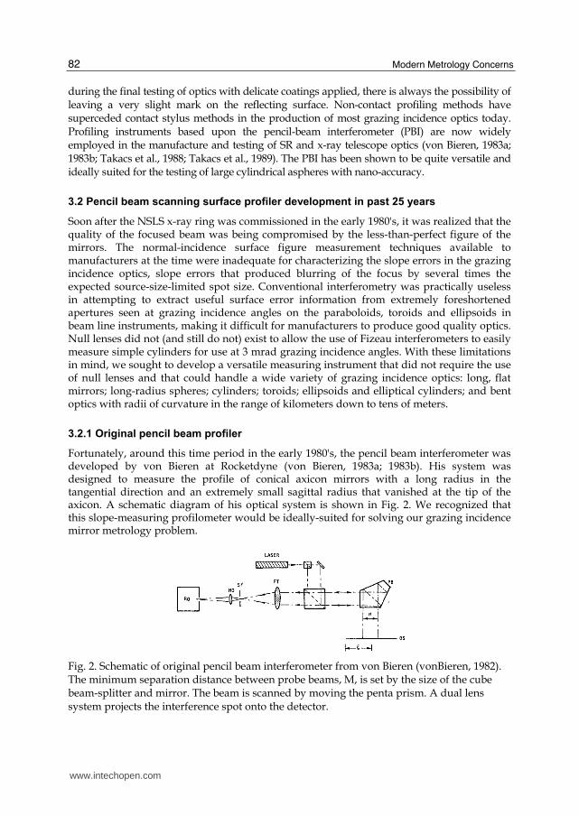
3.2.1 Original pencil beam profiler
Fortunately, around this time period in the early 1980's, the pencil beam interferometer was developed by von Bieren at Rocketdyne (von Bieren, 1983a; 1983b). His system was designed to measure the profile of conical axicon mirrors with a long radius in the tangential direction and an extremely small sagittal radius that vanished at the tip of the axicon. A schematic diagram of his optical system is shown in Fig. 2. We recognized that this slope-measuring profilometer would be ideally-suited for solving our grazing incidence mirror metrology problem.
Fig. 2. Schematic of original pencil beam interferometer from von Bieren (vonBieren, 1982). The minimum separation distance between probe beams, M, is set by the size of the cube beam-splitter and mirror. The beam is scanned by moving the penta prism. A dual lens system projects the interference spot onto the detector.
www.intechopen.com

Nano-Accuracy Surface Figure Metrology of Precision Optics 83
3.2.2 The Long Trace Profiler LTP I and LTP II
The Long Trace Profiler (LTP), based on the principle of the pencil-beam interferometer, was developed by Takacs and Qian and collaborators for the metrology of second-generation synchrotron radiation optics (Takacs et al., 1987; Takacs & Qian, 1989). Its operating principle is similar to that underlying an autocollimator, but with a laser pencil beam employed to scan the mirror being tested. The pencil beam is usually the direct output from a collimated laser diode or fiber-coupled laser. A schematic of the LTP optical system is shown in Fig. 3. The first beam-splitter produces a colinear pair of beams separated by a variable distance set by the adjustable prism. The separation distance can be adjusted from full overlap, M=0, to any desired value, while maintaining zero optical path difference (ZOPD) between the beams. The ZOPD system design is a vital improvement for a successful PBI profiler, because it eliminates the interference fringe movement due to the laser frequency shift (Qian & Takacs, 2004). This increases measurement accuracy significantly even when using an unstabilized laser. In contrast, the original von Bieren design had a very large OPD between the two beams. The ZOPD system allows the beams to be adjusted with a separation distance equal to the nominal 1mm beam diameter for maximum spatial frequency range information. The beam pair passes through the polarizing beam-splitter, PBS, and is split into a reference beam (REF) that is directed horizontally to a stationary mirror and a test beam that is directed down to the test surface. The return beams are focused onto a linear array detector by a Fourier transform lens, where each beam pair produces an interference pattern adjusted to have a minimum in the center. The position of the minimum on the detector, y, is proportional to the local slope of the surface between the two components of the beam pair:
F tan 2y (1)
where α is the local surface slope and F is the focal length of the lens. By scanning the beam across the mirror surface, the slope profile is measured, from which the height can be derived by integration. In the case of synchrotron optics for 2nd and 3rd generation machines, the slope error profile is a more useful measure of the surface quality for the end user, but the height profile is necessary for the manufacturer to use in correcting the surface.
Fig. 3. Schematic of the LTP-II optical system. The PBS generates a reference beam from a plane mirror fixed to the optical bench surface. Pitch error in the movement of the optical head on the air bearing is corrected by adding the signals from the test and reference arms.
www.intechopen.com

Modern Metrology Concerns 84
Some recent versions of the LTP use a single probe beam instead of the dual beam, eliminating the need for the initial beam splitting optics. The probe beam is focused to a single spot with no internal interference structure. The peak or centriod of the intensity distribution on the sensor determines the angle of the surface seen by the beam footprint. In this respect, the LTP operates very much like an autocollimator. Various algorithms are used to extract the centroid location of the spot with high precision.
Over the years, many improvements have been made to the original LTP-I design by many collaborators involved in synchrotron and x-ray telescope optics metrology. The original LTP system utilized an external electronic autocollimator to measure the pitch angle error of the optical head as it moved along the air bearing. The autocollimator was replaced by the internally-generated reference beam, shown in Fig. 3, by Irick, et al. (Irick et al., 1992) This allowed for simple correction of the measured profile for mechanical pitch errors by adding the two signals together. The relative intensity between the test and reference beams could now be adjusted easily by the use of polarizers and wave plates added to the optical system (not shown). The commercial version of the instrument, the LTP-II, produced by Continental Optical Corp. for several years, incorporated the internal reference beam and used a dual-array linear photodiode sensor as the detector. The dual array detector allowed the reference beam to be aligned nearly along the optical axis of the system instead of at an extreme angle, which places the spot at the end of the sensor. Having the reference beam centered in the lens aperture minimizes the introduction of phase shifts by glass inhomogeneities that translate into beam spot location variations with lateral movement of the beam across the aperture during a long scan. Bresloff added a Dove prism into the reference beam to change the phase of the laser pointing direction drift to be the same as the mechanical pitch angle error, allowing for correction of both error signals simultaneously by addition of the two signals (Takacs & Bresloff, 1986; Takacs et al., 1999).
Fig. 4. The LTP II optics board layout showing the 10 mrad surface slope acceptance angle optics in place. A 4-mirror arrangement folded the beams from the 1.25 m focal length lens with 7 reflections onto the detector mounted in back of the plane of the figure. The Dove prism mounted on the optics board in the REF arm inverted the phase of the pitch error signal to allow for simultaneous correction of pitch and laser drift
www.intechopen.com

Nano-Accuracy Surface Figure Metrology of Precision Optics 85
A sketch of the LTP-II optical head is shown in Fig. 4. This optical head used a Fourier transform lens with a focal length of 1.25 meters, which necessitated a folding mirror system to keep the size of the system within reason. The system was designed to measure surfaces with a total angular range of 10 milliradians. While this may seem like a small acceptance angle, it was sufficient to handle 99% of the long-radius optics used in NSLS beam lines. The LTP excels at measuring large flat and long-radius surfaces up to 1 meter in length. Other versions of the LTP-II can handle mirrors up to 1.5 meters long.
Improvements to the LTP-II and its successors, the LTP-IV and -V, manufactured by Ocean
Optics, eventually enabled reliable surface slope error measurements down to the 0.5 µrad
RMS level. However, recent advancements in synchrotron machine technology have resulted
in the need for mirrors with slope errors in the 100 nrad range in order to allow for nanometer
focal spot sizes. This quest for nano-accuracy in metrology has led to the development of
specially-engineered machines that must be used in thermally-stable special environments in
order to achieve this level of accuracy. The NOM machine developed at BESSY II in Germany
by Lammert and collaborators (Lammert et al., 2006; Siewert et al., 2004) is the prime example
of this next-generation profiler, which we will discuss in the next section.
3.2.3 Penta-prism LTP
The LTP II uses a scanning optical head (OH) in the tilted reference mode. Qian et al.
developed the scanning penta-prism mode LTP (PPLTP) in 1995 at Sincrotrone Trieste, Italy
(Qian, 1995), an evolution that extends applications and improves the accuracy of tests for
plane- and near plane-mirrors because a tilted reference beam is unnecessary. The main
characteristic of the penta-prism is: the angle between incident and output beams of the penta-
prism will always be equal to 2 is angle between two reflection surfaces of the penta-
prism, nominal angle is 45°), even if the penta-prism is tilted. So for a scanning penta-prism,
the slide pitch error will not influence output beam direction. This measurement method has
been successfully adopted by many SR metrology laboratories. In addition to accuracy
improvement, the penta-prism LTP has enabled the testing of in situ heat load distortion of
mirrors in vacuum chambers and the testing of small diameter aspheric surfaces of astronomy
telescopes by use of a derivative of the penta-prism LTP: the in-situ LTP and vertical scan LTP
(VSLTP). These will be described later. Also, the NOM employs a scanning penta-prism mode
to enhance accuracy to the nano-radian level in small test angles.
3.2.4 The multiple functions LTP (LTP-MF)
Qian has developed a Multiple Functions LTP (LTP-MF) that incorporates two compact LTP
optical heads into various configurations that allow for self-correction of scan-induced
errors with subsequent improvements in measurement accuracy (Qian et al., 2005; Qian &
Takacs, 2007). Some important facts of the LTP-MF, related to the approach to nano-
accuracy, are briefly described here. The LTP-MF can operate in the mode of scanning
optical head with non-tilted reference by use of a second optical head to ensure higher
accuracy (Fig. 5). If a high quality air-bearing system is used and 0.01°C temperature
stability can be maintained, the LTP-MF can achieve 0.1rad rms accuracy in testing plane
mirror surfaces. The LTP-MF can also operate in the penta-prism scanning mode for testing
nearly plane mirrors with high accuracy.
www.intechopen.com

Modern Metrology Concerns 86
Fig. 5. The LTP-MF collaborated between BNL (USA) and NSRL (China). The first optical head (OH) acts as scanning OH with non-tilted reference by use of the second OH. The second OH can also act as scanning penta-prism LTP
The schematic of the LTP-MF optical head is shown in Fig. 6. An unstabilized diode laser
(DL) with a 633nm wavelength with power of 1-5mW is used as the light source. The optical
fiber is used as a controllable beam transport tool. There are several advantages to using an
optical fiber: a) to achieve a compact and convenient package; b) to isolate the thermal
source from the optical system, which is helpful for achieving nano-accuracy; c) to minimize
laser beam pointing error; d) to change the light source wavelength with ease and to replace
the source without distorting the beam direction; e) to insert optical fiber devices in order to
perform various new functions, for example, adding a fiber attenuator for controlling
intensity. The beam is collimated to 1 mm diameter spot by a fiber collimator (FC). Then it
passes through a monolithic wave-front splitting beam splitter (WSBS) and becomes two
half-beam spots with a phase-shift so that when it is focused on the CCD by lens (FT), it
will produce an interference fringe with the shape of valley-at-center for low noise fitting.
The LTP-MF uses an equal optical path WSBS for the purposes of nano-accuracy and
compactness. Otherwise, the large frequency shifts of diode laser will produce the fringe
position shift, which will degrade the nano-accuracy. A pair of microscope cover plates are
constructed as an adjustable phase shift WSBS, which is the easiest and lowest cost solution
(Qian & Takacs, 2004; 2003)
The 20 x 20 mm PBS splits the beam into sample and reference arms, then they are reflected
back from the mirror under test and reference mirror to the FT lens which has a focal length
of 400 mm and a 28 mm aperture. The return beams are then focused onto a linear array
CCD of 14 m pixel size. Two quarter wave-plates (QWP) are for isolating unwanted
reflected beams, the half wave plate (HWP) is for adjusting the intensity ratio between the
sample beam and reference beam. However, in the case of using the scanning OH with non-
www.intechopen.com

Nano-Accuracy Surface Figure Metrology of Precision Optics 87
tilted reference, the HWP is unnecessary. Polarizer (P) is for adjusting the beam intensity,
but now it is easily replaced by a fiber attenuator. Two folding mirrors are for reducing the
overall mechanical length, but for new nano-accuracy profile they should be removed in
order to reduce systematic error. The FT lens is designed to keep aberrations below 1 µrad
for two scanning modes conditions. The PBS needs to be of extremely high quality,
including each surface, angles, and material uniformity to insure LTP precision. Good
alignment of the optical system will ensure measurement accuracy when the angular test
range is large.
Fig. 6. The optical system scheme of the multiple functions LTP (LTP-MF)
It is conceptually easy to enlarge the LTP measurement range by reducing the focal length of the FT lens, by increasing the CCD size, by using a high resolution CCD, or by enlarging the PBS and FT aperture size. However, if nano-accuracy is required over the entire angular test range, then the improvement task becomes extremely difficult.
3.2.5 The vertical scanning LTP (VSLTP)
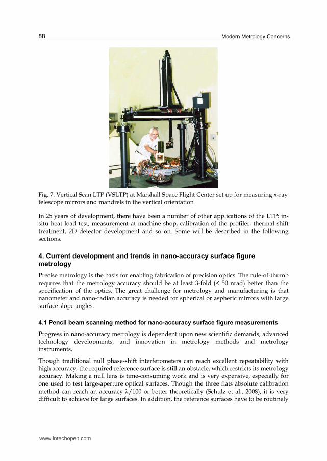
The mirrors used for X- ray telescopes are all based upon the use of grazing incidence optics in various configurations. Wolter Type I systems use a combination of paraboloidal and hyperboloidal surfaces; a Wolter-Schwarzchild Type I system consists of a small figure modification of a Wolter I system; the foil cone is an approximation of a Wolter I system, and the Kirkpatrick-Baez (K-B) system consists of two sets of orthogonal spheres or parabolic cylinders, produced by bending thin plates. The surface figures are generally conical in shape with very small sag deviations, on the order of microns, from the best-fit conical surface. These optics are ideally suited for measurements with the LTP. The ideal configuration for measuring x-ray telescope optics, however, is to measure the object while it is oriented with its symmetry axis in the vertical direction. This minimizes the effects of gravity-induced distortion on the surface figure, especially on thin shells or foil surfaces. A vertical scanning LTP (VSLTP), a modification of the scanning penta-prism LTP, was developed for testing X-ray telescope mirrors in the vertical orientation and is shown in operation in Fig. 7 (Li et al., 1996,1997). The benefit of the VSLTP is that a small penta-prism can be scanned inside a small diameter x-ray telescope mirror.
www.intechopen.com
Modern Metrology Concerns 88
Fig. 7. Vertical Scan LTP (VSLTP) at Marshall Space Flight Center set up for measuring x-ray telescope mirrors and mandrels in the vertical orientation
In 25 years of development, there have been a number of other applications of the LTP: in-situ heat load test, measurement at machine shop, calibration of the profiler, thermal shift treatment, 2D detector development and so on. Some will be described in the following sections.
4. Current development and trends in nano-accuracy surface figure metrology
Precise metrology is the basis for enabling fabrication of precision optics. The rule-of-thumb requires that the metrology accuracy should be at least 3-fold (< 50 nrad) better than the specification of the optics. The great challenge for metrology and manufacturing is that nanometer and nano-radian accuracy is needed for spherical or aspheric mirrors with large surface slope angles.
4.1 Pencil beam scanning method for nano-accuracy surface figure measurements
Progress in nano-accuracy metrology is dependent upon new scientific demands, advanced technology developments, and innovation in metrology methods and metrology instruments.
Though traditional null phase-shift interferometers can reach excellent repeatability with high accuracy, the required reference surface is still an obstacle, which restricts its metrology accuracy. Making a null lens is time-consuming work and is very expensive, especially for one used to test large-aperture optical surfaces. Though the three flats absolute calibration
method can reach an accuracy /100 or better theoretically (Schulz et al., 2008), it is very difficult to achieve for large surfaces. In addition, the reference surfaces have to be routinely
www.intechopen.com

Nano-Accuracy Surface Figure Metrology of Precision Optics 89
but inconveniently calibrated. As described above, the stitching methods accumulate small systematic interferometer errors that limit their high accuracy. Hence, the accuracy of measurements of a full-size surface with sub-aperture stitching method needs to be calibrated precisely
Pencil beam scanning methods have become a promising metrology method to make nano-accuracy surface profilers, because of their many advantages: non-contact test, absolute measurement without need of using a large reference, high accuracy, possibility of measuring large dimension optics and aspheric optics with moderate cost, and no need for working distance adjustment due to the use of a collimated beam. These advantages keep this method as one of most important solution for the optical metrology in the future even though it has a disadvantage of being only a one-dimension measurement with lower test speeds. The sub-aperture interferometer stitching method is beginning to be used with LTP and SR-optics measurements (Assoufid et al., 2004; Polack et al., 2010) with linear scanning. It will extend to large optics the ability to perform 2-D and mid-spatial frequency testing. However, improvements are needed in LTP stitching accuracy, along with research on precise calibration methods.
4.2 Various nano-accuracy profilers with scanning pencil beam method have been developed
The Nano-Optic-Measuring Machine (NOM, Fig. 8) (Lammert et al., 2006; Siewert et al., 2004) is the most accurate instrument so far for evaluating SR and other large optics. The NOM incorporates a special commercial autocollimator and an LTP optical head with a scanning penta-prism system to measure long-radius optics. It applies a small aperture of about 2 mm near the mirror under test in order to increase the spatial frequency range. The demonstrated uncertainty of the NOM in the measurements was low: for a plane mirror it was 0.05 μrad rms, and, for curved mirror, it was 0.2 μrad rms. Both instruments operate in a scanning penta-prism mode without the need to use a reference beam to correct for slide pitch error. A similar and improved Diamond-NOM has also been developed (Alcock et al., 2010).].
Fig. 8. The NOM, Courtesy of F. Siewert, T. Noll, T. Schlegel, T. Zeschke, H. Lammert, The nanometer optical component measuring machine: a new sub-nm topography measuring device for x-ray optics at BESSY, AIP CONFERENCE PROCEEDINGS Vol.705, 847-850 (2004)
www.intechopen.com

Modern Metrology Concerns 90
A new Traceable Multiple Sensor (TMS) system was developed by the Physikalisch-
Technische Bundesanstalt (PTB) for measurement with nanometer accuracy (Fig. 9) (Schulz
et al., 2010; Wiegmann et al., 2010; PTB Working Group 8.42, 2011). It encompasses coupled
multiple distance-sensors that are scanned along the surface under test. By using a small
sensor head, a high lateral resolution is achieved. In addition to the multiple distance
sensors, the TMS utilizes an autocollimator measuring the tilt of the sensor’s head, thereby
eliminating systematic errors in the distance sensors. The TMS can reach nanometer or
better accuracy with high lateral resolution. Both the NOM and TMS are suitable for plano
and near-plano mirror measurements with nano-radian accuracy. During a scan on a plane
mirror, the reflected beams are always parallel and remain steady except for very tiny angle
variations produced by the slope error on the surface. In this fixed beam direction condition
when testing plane mirrors, if the temperature is very stable and the scan system has very
small pitch, yaw and roll errors, the beam will not have any error that impacts the test
accuracy except for the noise. So it is possible to achieve nano-accuracy on plane surfaces
regardless of what instrument is used.
Fig. 9. Traceable multiple sensor (TMS) system, Courtesy of Schulz, G. Ehret, M. Stavridis, C. Elster, Concept, design and capability analysis of the new Deflectometric Flatness Reference at PTB, Nuclear Instruments and Methods in Physics Research A 616 (2010) 134–139
4.3 Difficulties to approach nano-accuracy metrology for large slope surfaces
Testing of strongly curved surfaces presents significant difficulties to pencil beam scanning profilers, as it does to most optical measuring techniques. In this case, measurement nano-accuracy is hard to reach in large part due to the impact of insufficient optical system quality of the profiler.
Let us analyze the beam position variation in the optical system during the
measurements. We use as an example a spherical mirror under test (MUT) scanned by the
scanning optical head of the LTP II (Qian, S. N. & Qian, K., 2010; Qian, 2011). The sample
beam (solid line, Fig. 10 a)) measures the slope of a MUT, and the reference beam (dashed
line) measures the air bearing pitch error. In order to avoid the overlapping of sample and
reference beams on the CCD, the LTP II reference beam is tilted to move the spot to one
end of the detector. During the scan both sample and reference beams have lateral
motions (BLM) over the optical components inside the optical head, shown as solid and
dashed shadow areas, which will pick up large local phase shift errors that show up as
surface slope error. These errors are produced by surface figuring error, inhomogeneity of
www.intechopen.com

Nano-Accuracy Surface Figure Metrology of Precision Optics 91
optical components, system aberration and system alignment errors. However, sample
beam lateral motion is an unavoidable condition in testing the slope of curved mirrors,
but we can effectively reduce the sample BLM magnitude by adopting a novel system
scheme.
In contrast the penta-prism scan mode (by use of the LTP optical head or autocollimator) has much larger BLM than scanning optical head (Fig.10 b), so it is not recommended for measuring larger slope optics.
(a) (b)
Fig. 10. a) Sample and reference beams’ lateral motion in scan optical head mode; b) Beams’ lateral motion on a scan in the penta-prism mode
How large is the slope error produced by the BLM? The following measurement compares a
tilted reference and a non-tilted reference. Two scans were done only with the reference arm
of the LTP III over a 900 mm length scan in sequence. The first scan is with a reference beam
angle of 1.5 mrad, which results in a 3 mm lateral motion across the PBS (Fig. 11 a);
the second scan is with a non-tilted reference beam (Fig. 11 b). The difference (Fig. 11 c))
between both scans is ±5 µrad (P-V) which is a serious slope error for a nano-radian surface
profiler. If the tilt angle increases due to strongly curved mirror, the systematic error of the
profiler will be more severe. Also, if the reference beam spot is displaced away from system
center even in the case of using a second linear CCD or 2D CCD, it will still produce
considerable BLM in vertical direction in 2-3 mrad angle level. This method should also not
be suitable for the nano-accuracy system. Results of several tests indicate that the magnitude
of the slope error caused by BLM could be larger than 1 rad rms. If the BLM is larger due to
the larger test angle, the error will increase quickly. The problem is that the real error is so
larger even though we use available highest quality optics, it is still not enough to reach
0.1 rad accuracy for strongly curved surface test. The following simulation analysis
illustrates this effect.
www.intechopen.com

Modern Metrology Concerns 92
Fig. 11. LTP III slope error produced by tilted reference: a) reference beam spot is tilted in 1.5 mrad; b) non-tilted reference beam at CCD center; and c) slope error caused by tilted reference.
4.4 Error simulation analysis of surface figure errors and inhomogeneity of profiler optics based on wave-front distortion
A sinusoidal wave-front is used to simulate the surface figure error and slope error. A
sinusoidal wave-front error of ±1nm (P-V) in 20 mm (Fig. 13 a) will produce ± 0.314 rad slope error (Fig. 12).
Fig. 12. Angle error produced by sine wave-front error of ±1 nm
4.4.1 Slope error produced by surface figure error
If a refractive surface figure error is a ±1 nm sine wave (/317), it will produce a sinusoidal
wave-front error of ±0.5nm and a slope error of 0.157rad for a material with an index of 1.5
(Fig. 13 b), which is a value large enough to destroy the nano-accuracy. If there are multiple
surfaces in the optical system, the error will be larger than 0. 1 rad.
If a reflective surface figure error has a sinusoidal error of ±1 nm, it will produce a reflective
sinusoidal wave-front error of ±2nm and a slope error of 0.628 rad (Fig. 13 c), which is a
much larger impact than a refractive surface.
The best surface figure quality typically available in customer optics is about /100 with
very high cost. This means that even if we use the highest quality available optics it will
probably not be easy to reach 0.1 rad accuracy.
-4 0
-3 0
-2 0
-1 0
0
1 0
2 0
3 0
4 0
-5 0 0 0 5 0 0
L T P I I I s lo p e e r ro r p ro d u c e d b y t i l te d r e fe r e n c e
slo
pe (
ura
d)
d is ta n c e (m m )
c )
b )
a )
-0.4
-0.3
-0.2
-0.1
0
0.1
0.2
0.3
0.4
0 5 10 15 20
Angle error produced by sine wavefront error of +/- 1 nm
slo
pe
(u
rad)
Distance (mm)
www.intechopen.com

Nano-Accuracy Surface Figure Metrology of Precision Optics 93
0.5 nm distorted wave-front
PBS, n=1.5
plane wave-front
a)
slope error
0.314 rad
1nmdistorted wave-front
PBS
b)
plane wave-front
2 nm distorted wave-front
1nm surface error
1nm suface errorc)
plane wave-front
Fig. 13. a) 1nm distorted wave-front and its slope error;
b) 1nm refractive surface error and its distorted wave-front;
c) 1 nm reflective surface error and its distorted wave-front
4.4.2 The slope error produced by inhomogeneity
The optical path difference (OPD) produced by glass inhomogeneity is
OPDh = n * path length (2)
where n is the refractive index error. Commercial optics typically use Grade H2 of
SCHOTT glass with n=5e-6 (SCHOTT, 2004). Assuming the refractive index variation has a
sinusoidal distribution in 20mm length and 2mm thickness layer, it will produce a 1.57rad
slope error. So grade H2 is not suitable for the nano-radian accuracy application. Grade H5
glass or Grade 0AA of Corning HPFS® glass (Corning, 2008) has an index variation of
n=5e-7, which will produce 0.157rad slope error. Actual error needs to verify with
practical test.
Most non-contact optical profilers that use optical systems for measuring angle variation
will confront with these difficulties if there is BLM. Examples of such systems are the optical
head of the LTP, the autocollimator of the NOM and optical system of the PTB’s profilers.
As a result of the above simulation analysis, it is necessary to apply the best quality glass
Grade H5 and /100 figured surfaces to achieve a nano-accuracy profiler. An actual error
estimation using the highest quality optics is underway.
4.4.3 Surface figure error in the mid-spatial frequency range and its metrology
Optical surface errors are general divided into three categories: a) low-spatial frequency
(LSF): as surface figure error; b) mid-spatial frequency (MSF): as ripple, and c) high
frequency: as surface finish roughness (Youngworth & Stone, 2000; Youngworth et al., 2008).
The low-spatial frequency surface error is defined over the spatial period range from 5-10
mm to the entire surface dimension, while the mid-spatial-frequency (MSF) surface error is
roughly defined in the range between 0.1 to 5-10 mm spatial periods. The impacts to the
optical system quality of both LSF and MSF can be analyzed with ray-based model. MSF
could also be considered as surface figure.
MSF will have a more severe impact on surface slope error than LSF error. The following sinusoidal wave-front simulations describe this effect. Fig. 14 shows simulated sinusoidal wave-fronts and their slopes (derivative of the wave-front) in a 20 mm surface length. The
wave-fronts have identical amplitudes of ±1nm, equal to /317, but with different
www.intechopen.com
Modern Metrology Concerns 94
frequencies. It is obvious that higher frequency waves have a much larger slope error than low frequency ones.
Fig. 14. Higher frequency wave-front has much larger slope error even though the amplitude of the wave-front is the same
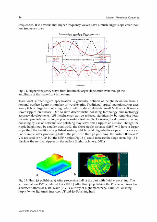
Traditional surface figure specification is generally defined as height deviation from a nominal surface figure in number of wavelengths. Traditional optical manufacturing uses long pitch or large lap polishing, which will produce relatively small MSF error. It means fewer ripples on surface. Due to new deterministic polishing technology and metrology accuracy developments, LSF height error can be reduced significantly by removing local material precisely according to precise surface test results. However, local figure correction polishing by use of deterministic polishing may leave small ripples on surface. Though the
ripple height may be smaller than 100, the short ripple distance (MSF) will have a larger slope than the traditionally polished surface, which could degrade the slope error accuracy. For example, after processing half of the part with fluid jet polishing, the surface flatness P-
V is reduced to /100, but the MSF ripples (Fig.15 a) could increase the slope error. Fig. 15 b) displays the residual ripples on the surface (Lightmachinery, 2011).
Fig. 15. Fluid jet polishing: a) After processing half of the part with fluid jet polishing. The
surface flatness P-V is reduced to /100; b) After fluid jet polishing the 4” silicon mirror has a surface flatness of 1/100 wave (P-V). Courtesy of Light machinery, Fluid Jet Polishing, http://www.lightmachinery.com/Fluid-Jet-Polishing.html
-4
-3
-2
-1
0
1
-2
0
2
4
6
8
0 5 10 15 20
Same amplitude waves have different slope errors:1hz is 0.314urad, 7hz is 2.20urad
height/1Hz(nm)Height/3Hz
Height/5HzHeight/7Hz
Slope/1hz(urad)
Slope/3hz
Slope/5hzSlope/7hz
hei
ght/
1H
z(nm
)S
lop
e/1hz(u
rad
)
distance (mm)
very different slope error vs. spatial frequency
same height error of 1nm
a b
www.intechopen.com
Nano-Accuracy Surface Figure Metrology of Precision Optics 95
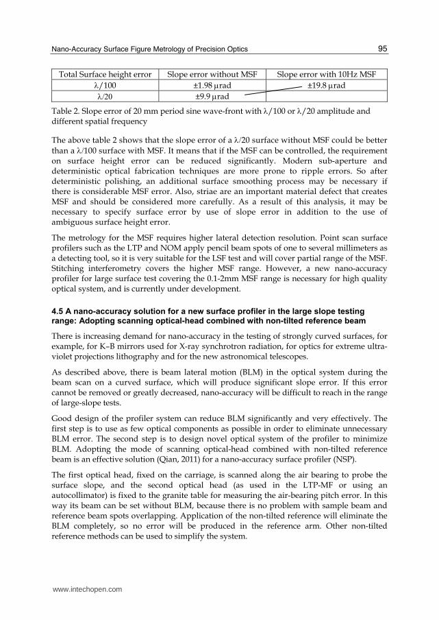
Total Surface height error Slope error without MSF Slope error with 10Hz MSF
/100 ±1.98 rad ±19.8 rad
±9.9 rad
Table 2. Slope error of 20 mm period sine wave-front with /100 or /20 amplitude and different spatial frequency
The above table 2 shows that the slope error of a 20 surface without MSF could be better
than a 100 surface with MSF. It means that if the MSF can be controlled, the requirement on surface height error can be reduced significantly. Modern sub-aperture and deterministic optical fabrication techniques are more prone to ripple errors. So after deterministic polishing, an additional surface smoothing process may be necessary if there is considerable MSF error. Also, striae are an important material defect that creates MSF and should be considered more carefully. As a result of this analysis, it may be necessary to specify surface error by use of slope error in addition to the use of ambiguous surface height error.
The metrology for the MSF requires higher lateral detection resolution. Point scan surface profilers such as the LTP and NOM apply pencil beam spots of one to several millimeters as a detecting tool, so it is very suitable for the LSF test and will cover partial range of the MSF. Stitching interferometry covers the higher MSF range. However, a new nano-accuracy profiler for large surface test covering the 0.1-2mm MSF range is necessary for high quality optical system, and is currently under development.
4.5 A nano-accuracy solution for a new surface profiler in the large slope testing range: Adopting scanning optical-head combined with non-tilted reference beam
There is increasing demand for nano-accuracy in the testing of strongly curved surfaces, for example, for K–B mirrors used for X-ray synchrotron radiation, for optics for extreme ultra-violet projections lithography and for the new astronomical telescopes.
As described above, there is beam lateral motion (BLM) in the optical system during the beam scan on a curved surface, which will produce significant slope error. If this error cannot be removed or greatly decreased, nano-accuracy will be difficult to reach in the range of large-slope tests.
Good design of the profiler system can reduce BLM significantly and very effectively. The first step is to use as few optical components as possible in order to eliminate unnecessary BLM error. The second step is to design novel optical system of the profiler to minimize BLM. Adopting the mode of scanning optical-head combined with non-tilted reference beam is an effective solution (Qian, 2011) for a nano-accuracy surface profiler (NSP).
The first optical head, fixed on the carriage, is scanned along the air bearing to probe the surface slope, and the second optical head (as used in the LTP-MF or using an autocollimator) is fixed to the granite table for measuring the air-bearing pitch error. In this way its beam can be set without BLM, because there is no problem with sample beam and reference beam spots overlapping. Application of the non-tilted reference will eliminate the BLM completely, so no error will be produced in the reference arm. Other non-tilted reference methods can be used to simplify the system.
www.intechopen.com

Modern Metrology Concerns 96
The first advantage of applying a scanning optical-head is to create the opportunity to use a short fixed working distance for the sample beam. In this way, the sample beam’s BLM can be significantly reduced to ±1mm (50 mm working distance) in comparison with ±20mm BLM in the scanning penta-prism mode for a test range of ±0.01 rad. This significantly lowers slope systematic error.
The second great advantage of applying a scanning optical head is its very simple calibration. Only one error compensation curve will be necessary to correct for all systematic errors for testing various mirrors. In contrast, it is very hard to compensate systematic errors in the penta-prism scanning mode, in which mirrors with different radius of curvature, different dimensions and different scanning start positions will need different compensation curves. Obviously, for a large test range, using the penta-prism scanning mode effectively precludes reaching nano-radian accuracy due to the BLM.
The third advantage of applying a scanning optical head is that small BLM and fixed working distance minimize the operational aperture of the lens, so it simplifies the aberration-reduction design of the lens. Another necessary approach to reduce systematic error is to improve the quality of the optical components including surface quality, optical material inhomogeneity and roughness.
Scan mode working distance (mm)
BLM(mm) /at test angle
Test angle (mrad)
Extra optics
Comment
Scan OH+ non-tilted REF (NSP)
Sample: 50 (fixed) Ref: 100-1100
Sample: ±0.5/±5mrad ±1/±10mrad Ref: 0
±10 N/A Larger test angle + high accuracy
Scan OH+ tilted REF (LTP II)
Sample: 50 (fixed) Ref: 100-1100
Sample: ±0.5/±5mrad Ref : ±10/±5mrad
±5 N/A Suitable for plane & near plane mirror test
Scan Penta-prism (PPLTP, NOM)
Sample: 300-1300
Sample: ±10/±5mrad
±5 Penta-prism /mirror
Suitable for plane & near plane mirror test
Table 3. Comparison of three scanning modes
Table 3 is the comparison of three scanning modes
Recently, the PTB described new research in “Scanning deflectometric form measurement avoiding path-dependent angle measurement errors” to reduce the BLM problem (Fig. 16) (Schulz et al., 2010). In the case of the PTB, the first autocollimator (AC1) beam is scanned through a penta-prism to the mirror under test (MUT). But the MUT is no longer stationary now, and it is tilted by a tilting stage in order to direct the reflected sample beam back along the incoming direction. This means that the MUT is tilted according to the slope at each scanning point. So this measurement arm incurs no BLM. The second stationary
www.intechopen.com

Nano-Accuracy Surface Figure Metrology of Precision Optics 97
autocollimator (AC2) is used to measure the tilt angle/slope of the MUT with a mirror fixed to the tilting stage. In this way, this tilting angle/slope test arm has a fixed short distance, which will reduce the BLM significantly (as in the case of the scanning optical head with non-tilted reference method). This is a good method to reduce measurement error caused by BLM.
Fig. 16. Principle of operation of the EADS system. AC1: Straightness representation and null instrument, AC2: angle measurement. Courtesy of M. Schulz et al. Scanning deflectometric form measurement avoiding path-dependent angle measurement errors, JEOS Rapid Publications 5, 10026 (2010)
The main principle and similar strategy in both cases of the scanning optical head with non-tilted reference method and the PTB method are: the probe arms to measure large tilted angles are short and fixed in order to reduce the BLM and are combined with another non-tilted beam arm in order to eliminate the BLM. As a matter of fact, in the PTB case, the angle tilt test is converted to a new arm by use of a tilting stage. However, a precision tilting stage must be used.
4.6 Summary of unresolved problems for nano-accuracy surface measurement
There are still many problems that need to be solved in the development of the NSP.
1. Further improvement in nano-accuracy: a 0.05 rad accuracy is expected
2. To ensure nano-accuracy (0.1rad rms) in the whole test range of 10 mrad (recent available test range) to 20 mrad (for strongly curved surface, like K-B mirror)
3. Except for stitching method, surface figure metrology of middle-spatial frequency of 0.1mm-2mm is necessary. It means to develop a NSP to span the measurement spatial frequency range from 0.1 mm to 1 meter on one scan.
4. For full 2D testing, now it is necessary to make parallel lines scans and multiple intersectional scans in order to establish the relations for every scanning point. It is better to obtain the slopes in both X and Y directions at every scanning point simultaneously. In this way measurement accuracy and time could be further improved.
5. In situ and cost-effective nano-accuracy calibration system development is necessary
www.intechopen.com

Modern Metrology Concerns 98
5. Calibration of nano-accuracy
As described above, now the required measurement accuracy is nano-radian and
nanometer. If the instrument cannot be calibrated precisely, nano-accuracy metrology
achievement is meaningless. Plane mirror measurement by use of traditional phase shift
interferometer is difficult to reach /50-/100 accuracy because of the reference surface
accuracy limitations. The absolute flatness test of the plane mirror by use of three-flat test
method can reach /100 or better, but it is very difficult for large mirror calibration (for
example for 500mm to 1000mm dimension). Pencil beam profilers can solve this problem,
but it is only in 1-D. When the tested slope range increases, the angle related systematic
error of the measurement instrument increases significantly. Though the pencil beam
profilers have potential power to reach nano-radian and nanometer accuracy or less in
principle, they still need to be calibrated. Calibration equipment should have the accuracy of
three times better than the instrument to be calibrated. This is a great challenge to optical
metrology.
5.1 Angle calibration system based on trigonometric function
Sine bar and tangent bar methods can be used to precisely measure small angles.
5.1.1 Sine bar
The sine bar is a simple and effective method in calibrating small angles. Sine bar system
contains one solid bar and two fixed-distance cylinders. When one cylinder B is lifted in a
height (h), while another cylinder A is kept in contact with the base surface (Fig. 17), the bar
rotation angle will be:
= arc sin (h/L) (3)
If the roundness and diameter of two cylinders are very precise, and their geometric
positions and moving height are accurate, the angle can be calculated very accurately. The
distance error of two cylinders is a systematic error, which can be eliminated easily by
calibration. The sine bar technology is able to reach nano-radian accuracy level.
The sine bar system known as the small angle generator with a length of about 523 mm at
National Physical Laboratory (NPL) of Britain is used for autocollimator and small angle
calibration (NPL, 2010). Its uncertainty is estimated to be ± 0.03 second of arc for angles in
the range ± 10 minutes of arc. It is suitable for nano-radian profiler calibration in this angle
range. For larger angle calibration the accuracy needs to improve.
The height lifting of a traditional sine bar is made by inserting a precise gauge block under
one of the sine bar cylinders, or by use of micrometer. However, the process of cleaning and
wringing of gauge blocks and support surface is time consuming and is not very reliable for
reaching nano-accuracy. The gauge block accuracy is 50nm. Generally the average wringing
film thickness between the gauge blocks is about 10 nm, but some wrings will be over 25
nm. For a non-professional operator the error could be much larger. A 30 nm possible height
error with 250mm bar length will produce 0.12 rad error. If this error is combined with
several other errors, it will impact the final nano-accuracy.
www.intechopen.com
Nano-Accuracy Surface Figure Metrology of Precision Optics 99
Fig. 17. Sine bar calibration scheme: = arc sin (h/L)
A computer controlled height lifting device and nanometer accuracy encoder are desired in order to reach nano-accuracy and to maintain temperature stability during the operation. The accuracy of mechanical and contacted Heidenhain length gauge is 30 nm. But its contact characteristic and insufficient accuracy will restrict nano-accuracy development of the sine bar system.
5.1.2 Tangent bar
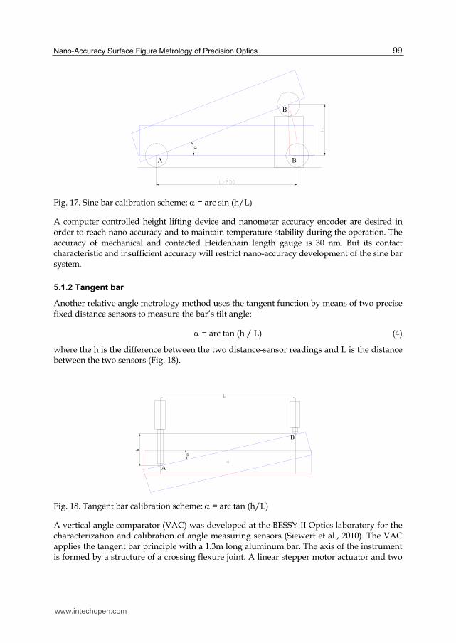
Another relative angle metrology method uses the tangent function by means of two precise fixed distance sensors to measure the bar’s tilt angle:
= arc tan (h / L) (4)
where the h is the difference between the two distance-sensor readings and L is the distance between the two sensors (Fig. 18).
Fig. 18. Tangent bar calibration scheme: = arc tan (h/L)
A vertical angle comparator (VAC) was developed at the BESSY-II Optics laboratory for the characterization and calibration of angle measuring sensors (Siewert et al., 2010). The VAC applies the tangent bar principle with a 1.3m long aluminum bar. The axis of the instrument is formed by a structure of a crossing flexure joint. A linear stepper motor actuator and two
A B
B
A
B
h
L
www.intechopen.com

Modern Metrology Concerns 100
linear encoders (Heidenhain CertoCP 60 K) enable a controlled tilting of the VAC. The linear encoder provides a constant uncertainty of ±50nm over a range of 60mm. The measuring resolution of the Certo is ±5 nm; this corresponds to a tilting resolution of about 10 nrad. The
achievable angular resolution of the VAC is about 0.015 rad, limited by the performance of the linear stepper motor. The error budget of the VAC is estimated to 50nrad rms.
Recent developments in precise interferometric distance sensors has improved measurement accuracy to the one nanometer level, which significantly increases the reliability for trigonometric function calibration. The displacement interferometer can be used for small angle metrology. Fig. 19 is the example that uses a ZYGO system (ZYGO, 2003). The difference of two distance sensor readings divided by the distance between two points is the tilt angle. Its advantages are non-contact and nanometer accuracy. The National Research Council Canada uses this principle in their angle calibration systems (Pekelsky & Munro, 2005).
Fig. 19. Displacement Measuring Interferometers, Courtesy of ZYGO, http://www.zygo.com/?/met/markets/stageposition/zmi/
The fiber-based Fabry-Perot interferometer (FFPI) is a typical multiple-beam interferometer that can be used as a non-contact distance sensor. The space separating the reflecting surface is called the cavity length. The reflected light in the FFPI is wavelength modulated in exact accordance with the cavity length (Pullteap, 2010). The attocube’s ultra-high precision displacement FPSsensor has a repeatability of 1 nm at 20 mm cavity length, making it is suitable for small angle calibration with sine bar or tangent bar due to the advantages of high accuracy and non contact measurement characteristic (Attocube, 2010). Assuming its
accuracy is 3 nm and it is used with a 250 mm sine bar, the error will be 0.012 rad. In addition, its very compact size is very attractive. However, larger test angles will impact the test accuracy significantly.
5.2 Calibration by use of commercial angle testing devices
Instrument calibration with nano-accuracy can be done by use of commercial angle measuring instruments such as the theodolite, goniometer and other angle measurement
www.intechopen.com

Nano-Accuracy Surface Figure Metrology of Precision Optics 101
devices. However, they provide nanometer resolution or nanometer repeatability but rarely are nano-accuracy. They can not be used for nano-accuracy calibration over large angular ranges. There are only a few angle calibration devices that have been developed that can reach high accuracy with a large angular test range, which is expected by surface profiler.
The first calibration of the LTP angle error was made at ELETTRA in Italy in 1995 by use of a precision theodolite, Leica Wild T3000, with a sensitivity of 0.1" (Qian et al., 2000). A small mirror M is fixed on the theodolite telescope in order to reflect the beam back to the LTP (Fig. 20). In this way we can know the mirror rotation angle precisely. The LTP records a stability scan as a function of time while the theodolite is rotated step by step with a separation of 0.1° or 0.05°. A step-like slope file can be obtained. The differences between the LTP angle values and theodolite reading angles determine the calibration angle error. By changing the LTP scale factor coefficient, e, the LTP angles can be adjusted. This is an absolute angle calibration. This test should be done after the precise adjustment of focal
plane position has been done. 0.1 arc second (0.5 rad) was suitable for 1 rad accuracy calibration at that time but it is not sufficient for recent nano-accuracy calibration requirements unless a higher accuracy theodolite is available.
Fig. 20. Setup of precise LTP angular calibration: WILD T3000 is used as an accurate angle generator. While The LTP is making stability scan and data acquisition continuously, the theodolite angle is changed step by step
The PTB angle comparator is the most accurate standard angular measuring device today with a test range of 360 degrees (Probst et al., 1998). It is well suited for pencil beam profiler calibration, especially for the larger slope profiler test. The angle-measuring system of the comparator consists of a ring-shaped index disc of glass with a radial reflected-light phase grating with 217 = 131 072 graduation periods on a circle approx. 400 mm in diameter. Eight scanning heads uniformly distributed over the circumference of the graduation are used for scanning this graduation. 218 = 262 144 signal periods are formed in each scanning head, which corresponds to an angular period of approximately 5". Digital interpolation of the signal period with the factor 2¹² = 4096 finally furnishes 2³º = 1 073 741 824 measurement steps per 360°, which corresponds to an angle-measuring step of approx. 0.0012" per scanning head. The angle value measured is finally obtained by averaging over all scanning heads. At present, this angle comparator allows an uncertainty of measurement of 0.005" (k = 2) to be reached.
LTP
(LTP drawing is rotated 90 degrees [top view]
in order to show reflecting beam)
WILD T 3000
M
FT Detector
www.intechopen.com

Modern Metrology Concerns 102
Angular calibrations of profilers can be made at national standards bureaus. However, for
researchers involved in precision angular R&D projects, it is necessary to check the nano-
radian accuracy of a profiler frequently, and for calibration at remote sites, a low cost
precision angle calibration device is desired.
In the case of sine bar and tangent bar systems for large angle measurements, the contact
surface in using mechanical length gauge or reflection mirror surface in interferometric
distance sensor is tilted. This will degrade the measurement accuracy considerably.
6. Precision metrology of in-situ and at-wavelength
Most measurements for precision optics are made in controlled environment in order to
verify compliance with specifications. However, the actual in-situ use of the optical
components could be very different from the laboratory condition. Beam quality and
position can be affected by temperature instability, distortion under high vacuum
condition, a noisy vibration environment, and thermal distortion due to absorption of
high power beams from synchrotron and FEL sources. In these cases, on-line figure
measurement of bending mirrors and adaptive optics is highly desirable. The
manufacturing of large astronomical optical components with nanometer accuracy
requires in-situ testing without removing the optics from the polishing machine. These in-
situ situations present challenges to the metrology. Most of these metrologies are having
increasing demands on nanometer level.
Owing to the restricted conditions for measurements on in-situ optics, very few
measurements have been made, even though they are very important.
6.1 In-situ X-ray mirror thermal distortion measurement
Mirror distortion under high heat load has been recognized as a serious problem for third-
generation synchrotron light sources, as well as for the first- and second-generation sources
operating under conditions of reduced emittance, high current and with novel insertion
devices. Efforts have been made at reducing mirror distortion by the use of high thermal
conductivity or low expansion materials, cryogenic cooling, enhanced heat exchangers, jet
cooling, and other means. Model calculations based on finite element design codes are used
to predict distortion theoretically. However, the performance of any mirror will ultimately
be determined experimentally when fully illuminated by the high power synchrotron beam,
because the practical boundary conditions usually differ from the ideal theoretical
conditions. An in-situ distortion test is then very useful for confirming the theoretical
calculations. A precise measuring method to detect the in-situ distortion profile of a high
heat load mirror for synchrotron radiation by use of the penta-prism Long Trace Profiler
was developed in 1995 in Italy. A schematic diagram of the heat-load measurement
equipment of the in situ LTP is shown in Fig. 21 (Qian et al., 1997, 1995). The optical head of
the LTP II profiler is mounted horizontally on an optical table (TB). The first penta-prism
(PT1) scans the sampling beam (SB) along the mirror under test (MUT) by use of a
mechanical translation slide (MS) fixed to TB with a 250-mm travel length. The reference
beam (RB) is directed onto a fixed spot on the MUT by a mirror (M1) and another penta-
prism (PT2). This spot is located along the center of the length of the mirror but displaced by
www.intechopen.com

Nano-Accuracy Surface Figure Metrology of Precision Optics 103
15 mm transversely toward the edge. For symmetry reasons this point should not have a
tangential slope variation component even if the mirror is subject to a high heat load.
Fig. 21. Schematic of the in situ LTP test on beam line
A maximum distortion of 0.47 µm over a length of 180 mm was measured for an internally water-cooled mirror on an undulator beam line at ELETTRA while exposed to a total emitted power of 600 watts (Fig. 22). For this measurement, the configuration with all of the equipment external to the vacuum chamber was used. The experiment has an accuracy and repeatability of 40 nm.
0
0.1
0.2
0.3
0.4
0.5
0 40 80 120 160
Thermal distortion test at ELETTRA, Italy, 1995
dis
tort
ion
(m
)
distance (mm)
150W
600W
360W
no
Fig. 22. In situ height distortion profiles of a synchrotron radiation mirror under a high heat load, as measured with the ppLTP: (a) Total power, 600W; undulator gap, 30mm; current, 181mA; energy, 2Gev. (b) Total power, 360W; undulator gap, 40mm; current, 187mA; energy, 2Gev. (c) Total power, 150W; undulator gap, 60mm; current, 224mA; energy, 2Gev.
(d) No synchrotron beam on, thus corresponding to the test repeatability (<0.04m, peak to valley)
The second thermal distortion test was done at The Advanced Photon Source (APS) at Argonne National Laboratory on the second mirror of SRI-CAT 2-ID-C beam line in 1997 (Takacs et al., 1998). The in-situ LTP scanned the central 90 mm of the 200 mm long mirror through a vacuum window while the mirror was subjected to heat loading from the
www.intechopen.com
Modern Metrology Concerns 104
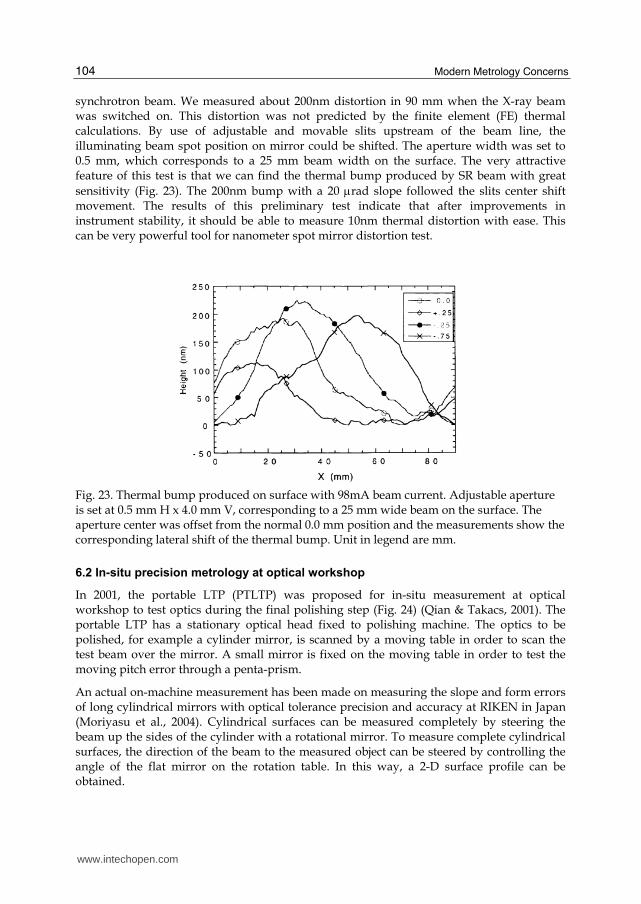
synchrotron beam. We measured about 200nm distortion in 90 mm when the X-ray beam was switched on. This distortion was not predicted by the finite element (FE) thermal calculations. By use of adjustable and movable slits upstream of the beam line, the illuminating beam spot position on mirror could be shifted. The aperture width was set to 0.5 mm, which corresponds to a 25 mm beam width on the surface. The very attractive feature of this test is that we can find the thermal bump produced by SR beam with great
sensitivity (Fig. 23). The 200nm bump with a 20 rad slope followed the slits center shift movement. The results of this preliminary test indicate that after improvements in instrument stability, it should be able to measure 10nm thermal distortion with ease. This can be very powerful tool for nanometer spot mirror distortion test.
Fig. 23. Thermal bump produced on surface with 98mA beam current. Adjustable aperture is set at 0.5 mm H x 4.0 mm V, corresponding to a 25 mm wide beam on the surface. The aperture center was offset from the normal 0.0 mm position and the measurements show the corresponding lateral shift of the thermal bump. Unit in legend are mm.
6.2 In-situ precision metrology at optical workshop
In 2001, the portable LTP (PTLTP) was proposed for in-situ measurement at optical workshop to test optics during the final polishing step (Fig. 24) (Qian & Takacs, 2001). The portable LTP has a stationary optical head fixed to polishing machine. The optics to be polished, for example a cylinder mirror, is scanned by a moving table in order to scan the test beam over the mirror. A small mirror is fixed on the moving table in order to test the moving pitch error through a penta-prism.
An actual on-machine measurement has been made on measuring the slope and form errors of long cylindrical mirrors with optical tolerance precision and accuracy at RIKEN in Japan (Moriyasu et al., 2004). Cylindrical surfaces can be measured completely by steering the beam up the sides of the cylinder with a rotational mirror. To measure complete cylindrical surfaces, the direction of the beam to the measured object can be steered by controlling the angle of the flat mirror on the rotation table. In this way, a 2-D surface profile can be obtained.
www.intechopen.com

Nano-Accuracy Surface Figure Metrology of Precision Optics 105
Fig. 24. Proposed in situ test at workshop in 2001
6.3 At wavelength metrology
Traditional optical metrology generally employs visible light as the illumination source, which is convenient and cost-effective. Recent developments in optics for extreme ultraviolet (EUV) lithography, x-ray synchrotron radiation optics, and free electron lasers operated at EUV and x-ray wavelengths place extraordinary requirements on the visible light metrology systems. Speer and collaborators(Harris et al., 1982; Speer et al., 1980) employed the point diffraction interferometer to perform at-wavelength measurements on grazing incidence optics into the far ultraviolet region. Sommargren, Goldberg and collaborators (Medecki et al., 1996; Tejnil et al., 1997; Sommargren 1996; Goldberg et al., 1995) extended the technique into the EUV region to test zone plate wave-fronts and Schwarzschild optics quality in the 13nm wavelength region. This work was driven by the need to produce multilayer-coated normal incidence optics that were diffraction-limited at wavelengths to be used in soft x-ray projection lithography. A 0.5nm wave-front error is
much more easily seen with a 13nm source, where it is /26, than with a 633nm HeNe
source, where it is more than /1000.
The point diffraction interferometer requires a system that produces a point focus somewhere along the optical axis. A more general method for testing x-ray wave-fronts was developed by Weitkamp and collaborators (Weitkamp et al., 2005) utilizing Talbot effect Moire fringes generated by phase and absorption gratings. The interferometer can be placed anywhere downstream of an optical element where it is convenient, making it a very
versatile technique. Wave-front distortions in the range of /100 can be measured, where = 0.1 nm, and surface slope errors can be detected with an accuracy of better than 100 nrad over spatial periods from 1mm to 1 m.
www.intechopen.com

Modern Metrology Concerns 106
Another versatile at-wavelength technique has been developed by Souvorov (Souvorov et al., 2002) and by Yumoto(Yumoto et al., 2006) and their coworkers, based upon the phase retrieval algorithms of Fienup (Fienup, 1982). By measuring the intensity variations in propagating x-ray beams downstream from a reflection or transmission element, the phase of the wave-front can be computed and projected back to the surface of the optical element. Yumoto has shown that surface figure errors measured by visible light interferometric means and by the phase retrieval methods agree to better than 1.5 nm on an 80mm long mirror. This method has the advantage over visible light interferometry in that it is sensitive to errors in the multilayer coatings on the optics, resulting in a measurement of the actual performance of the optic rather than just the profile of the top-most surface layer.
7. Thermal stability
7.1 Temperature stability requirement of ±0.01°C to ensure the 0.1µrad rms accuracy
After much experience with LTP stability scan measurements, we have seen that thermal
variation has a significant impact on the ability to achieve 0.1 µrad rms slope error
measurements. One can clearly see that slope error variations follow temperature
fluctuations. Some precision profiler measurements require averaging of several tens of
repeated measurements in order to achieve 0.1µrad accuracy, and 2-D testing also requires
much longer scanning time for multiple lines measurements in X and Y directions. In
addition, the thermal drift effects are always delayed for one hour or more. So we use a 15
hour stability scan test as the standard procedure to verify measurement stability.
Fig. 25 is a stability comparison measurement between the LTP II and the PTLTP made at NSRRC in Taiwan (Qian & Wang, 2005). Test beams are sent from both LTP II and PTLTP to the same test point on the mirror through comparison unit, and then each reflected beam is divided into two beams back to two LTPs individually.
Fig. 25. Stability comparison test between the LTP II and the PTLTP made at NSRRC in Taiwan
Four files of stability scan are obtained simultaneously. Each LTP receives two reflected beams sent from itself and from the other. Fig.26 a) is the temperature oscillation during the test. Fig. 26 b) is the slope errors of 4 stability scans. 2 large slope error curves are: beam is sent from LTP II; and 2 small slope error curves are: beam is sent from PTLTP no matter it is accepted by which LTP. These indicate: a) Slope error exactly follows temperature fluctuation period but with some delay; b) The LTP II has large stability error due to adopting unstable non-monolithic beam splitting structure; c) When temperature oscillation
www.intechopen.com

Nano-Accuracy Surface Figure Metrology of Precision Optics 107
dropped to ±0.01°C (flat section of the temperature curve), the stability over 15 hours was
below 0.1rad rms.
Fig. 26. a) LTPs temperature during the stability scan (without enclosure); b) Stability comparison test: 1) 2 large slope error curves: beam is sent from LTP II; 2) 2 small slope error curves: beam is sent from PTLTP
Another stability measurement with an f=150mm LTP had a larger slope of 0.17rad rms
due to larger temperature variation of 0.07°C (Fig. 27 a). The Fig. 27 b) shows the 0.156 rad
rms stability test of 15 hours in X-direction with an improved 2D CCD system (f’=400 mm)
while temperature variation of 0.2 °C (P-V). These stability measurements verify that the
±0.01°C temperature stability is necessary to ensure much less stability slope error than
0.1rad rms.
Fig. 27. a) Stability tested over 15 hours on f=150mm LTP with temperature variation of 0.07°C; b) The 15 hours stability test in X-direction with an improved 2D system (f’=400 mm) while temperature variation of 0.2 °C (P-V)
7.2 Error reduction caused by thermal or mechanical drift
Recently, Yashchuk has developed measurement techniques that correct for slow thermal and mechanical drift errors that are inherent in typical LTP measurements (Yashchuk, 2009). His methods involve making a series of measurements on a surface in the forward and
- 3 0
- 2 0
- 1 0
0
1 0
2 0
3 0
0 1 0 0 2 0 0 3 0 0 4 0 0 5 0 0 6 0 0
Slo
pe
erro
r (m
rad)
T i m e t o t a l 9 h o u r s
P T L T P t o T W L T P ( 0 . 8 7 r a d r m s )
T W L T P t o T W L T P ( 8 . 9 r a d r m s )
T W L T P t o P T L T P ( 9 . 0 r a d r m s )
P T L T P t o P T L T P ( 0 . 9 7 r a d r m s )
21.5
22
22.5
0 100 200 300 400 500
Tem perature during com parison test in NSRRC(20516TW .tem, 5/16/02/22:46-5/17/02/07:46)
Deg
ree
(C)
Time (1' / pts)
Peak to valley: 0.5 (+/- 0.25) degree
a) b)
拒 拠拒拒 挙拒拒 渠拒拒 虚拒拒 許拒拒 距拒拒 鋸拒拒 漁拒拒 禦拒拒去拒居虚
去拒居渠
去拒居挙
去拒居拠
拒
拒居拠
拒居挙
拒居渠
況i勤 業 級拠許H 牛 距拒"巨錦巾i均琴糾
橋僅巾錦業 級禁ra暁糾
a) b)
www.intechopen.com
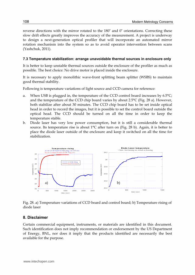
Modern Metrology Concerns 108
reverse directions with the mirror rotated to the 180˚ and 0˚ orientations. Correcting these slow drift effects greatly improves the accuracy of the measurement. A project is underway to design a next-generation optical profiler that will incorporate an automated mirror rotation mechanism into the system so as to avoid operator intervention between scans (Yashchuk, 2011).
7.3 Temperature stabilization: arrange unavoidable thermal sources in enclosure only
It is better to keep unstable thermal sources outside the enclosure of the profiler as much as possible. The best choice: No drive motor is placed inside the enclosure.
It is necessary to apply monolithic wave-front splitting beam splitter (WSBS) to maintain good thermal stability.
Following is temperature variations of light source and CCD camera for reference:
a. When USB is plugged in, the temperature of the CCD control board increases by 6.5°C; and the temperature of the CCD chip board varies by about 2.5°C (Fig. 28 a). However, both stabilize after about 30 minutes. The CCD chip board has to be set inside optical head in order to record the images, but it is possible to set the control board outside the optical head. The CCD should be turned on all the time in order to keep the temperature stable.
b. Diode laser has very low power consumption, but it is still a considerable thermal source. Its temperature rise is about 1°C after turn on (Fig. 28 b). Again, it is better to place the diode laser outside of the enclosure and keep it switched on all the time for stabilization.
Fig. 28. a) Temperature variations of CCD board and control board; b) Temperature rising of diode laser
8. Disclaimer
Certain commercial equipment, instruments, or materials are identified in this document. Such identification does not imply recommendation or endorsement by the US Department of Energy, BNL, nor does it imply that the products identified are necessarily the best available for the purpose.
2 3 .2
2 3 .4
2 3 .6
2 3 .8
2 4
2 4 .2
0 5 0 0 1 0 0 0 1 5 0 0
D io d e L ase r te m p e ra tu re
< 5m w , Ju s t tu rn in g o n , tes ted o n h o u sin g
tem
per
ature
(L
C)
t im e (sec )
2 3
2 4
2 5
2 6
2 7
2 8
2 9
3 0
0 5 0 0 1 0 0 0 1 5 0 0 2 0 0 0 2 5 0 0 3 0 0 0
1 C C D C h ipC o n tro l b o a rd
t im e (se c )
tem
per
ature
(L
C)
T e m p e ra tu re r is in g
a ) o n C C D b o a rd (U S B p lu g : o n -o ff -o n )
b ) o n C o n tro l b o a rd (U S B P lu g o n )
a) b)
www.intechopen.com

Nano-Accuracy Surface Figure Metrology of Precision Optics 109
9. Acknowledgment
Notice: This manuscript has been authored by Brookhaven Science Associates, LLC under Contract No. DE-AC02-98CH10886 with the U.S. Department of Energy. The United States Government retains, and the publisher, by accepting the article for publication, acknowledges, a world-wide license to publish or reproduce the published form of this manuscript, or allow others to do so, for the United States Government purposes.
10. References
Alcock, S., K. Sawhney, K., & Scott, S. (2010). The Diamond-NOM: A non-contact profiler
capable of characterizing optical figure error with sub-nanometre repeatability,
Nuclear Instruments and Methods in Physics Research, A 616, 224-228
Assoufid, L., Kim, K., Macrander, A. T., Lindberg, R., Kewish C. M., & Chubar, O., Requirements for Grazing-Incidence Mirrors for Hard X-ray Free-Electron Laser
Oscillator, http://www.esrf.eu/events/conferences/SMEXOS /PosterAssoufid
Assoufid, L., Bray, M., Shu, D. (2004). Development of a Linear Stitching Interferometric
System for Evaluation of Very Large X-ray Synchrotron Radiation Substrates and
Mirrors, Eighth International Conference on Synchrotron Radiation Instrumentation. AIP
Conference Proceedings, V.705, 851-854.
Attocube systems, http://www.attocube.com/attoMETROLOGY/attoFPSensor.htm, 2010
Bhushan, B., Wyant, J.C., & Koliopoulos, C.L. (1985). Measurement of surface topography of
magnetic tapes by Mirau interferometry, Applied Optics 24(10), p. 1489-1497.
Becker, K. & Heynacher, E. (1987). M400 - A coordinate measuring machine with 10 nm
resolution, in In-process Optical Metrology for Precision Machining, Proc. SPIE 802. pp.
209-216, presented at SPIE Symposium, The Hague, Netherlands,
Corning HPFS® glass, 2008.
http://www.corning.com/specialtymaterials/products_capabilities/HPFS.aspx
DeCew, A.E., Jr. & Wagner, R.W. (1986). An optical lever for the metrology of grazing
incidence optics, in Optical Manufacturing, Testing, and Aspheric Optics, Proc. SPIE
645. pp. 127-132, Orlando, FL, 1-2 April 1986.
Ennos, A.E. & Virdee, M.S. (1982). High accuracy profile measurement of quasi-conical
mirror surfaces by laser autocollimation, Precision Engineering 4, p. 5-9.
Engineering Synthesis Design Inc. (ESDI), Simultaneous Phase-Shifting for Vibration
Intensive & Turbulent Environments, 2011
http://www.engsynthesis.com/pdfs/ESDI_intellium_H2000_DS.pdf
Fleig, J., Dumas, P., Murphy, P.E., and Forbes, G.W. (2003). An automated sub-aperture
stitching interferometer workstation for spherical and aspherical surfaces, in Proc
SPIE 5188, eds. A. Duparre and B. Singh. pp. 296-30
Fienup, J.R. (1982). Phase Retrieval Algorithms - a Comparison, Applied Optics 21(15), p.
2758-2769.
Goldberg, K.A., et al. (1995). At-Wavelength Testing of Optics for EUV, Proc. SPIE 2437, pp.
347-354.
Heynacher, E. and Reinhardt, D. (1979). Measuring equipment for testing the directrix of
high-resolution Wolter-type telescopes, Proc. SPIE 184, p. 167-169
www.intechopen.com

Modern Metrology Concerns 110
Harris, W., Mrowka, S., and Speer, R.J. (1982). Linnik Interferometer - Its Use At Short
Wavelengths, Applied Optics 21(7), p. 1155.
Irick, S.C., McKinney, W.R., Lunt, D.L., & Takacs, P.Z. (1992). Using a straightness reference
in obtaining more accurate surface profiles from a long trace profiler for
synchrotron optics, Review of Scientific Instruments 63(1), p. 1436-1438.
Koliopoulos, C.L. and Wyant, J.C. (1980). Profilometer for Diamond-Turned Optics Using a
Phase-Shifting Interferometer, Journal of the Optical Society of America 70(12), p. 1591.
Kim, K., An X-Ray FEL Oscillator: Promises and Challenges, Workshop on Physics and
Applications of High Brightness Electron Beams, November 16-19, 2009
Kwang-Je Kim, An X-Ray FEL Oscillator: Promises and Challenges, Workshop on Physics and
Applications of High Brightness Electron Beams, November 16-19, 2009
Liu, Y.M., Lawrence, G.N., and Koliopoulos, C.L. (1988). Sub-aperture testing of aspheres
with annular zones, Applied Optics 27(21), p. 4504-4513.
Lammert, H., Siewert, F., & Zeschke, T. (2006). The Nano-Optic-Measuring Machine NOM
at BESSY - further improvement of the measuring accuracy, in BESSY Annual
Report 2005. BESSY GmbH: Berlin, Germany. p. 481-486.
Li, H., Li, X., & Grindel, M.W. (1996). Measurement of X-ray Telescope Mirrors Using A
Vertical Scanning Long Trace Profiler, Opt. Eng. 35(2), p. 330-338.
Li, H., Takacs, P.Z., & Oversluizen, T. (1997). Vertical scanning long trace profiler: a tool for
metrology of x-ray mirrors, Proc. SPIE 3152. pp. 180-187.
Lightmachinery, Fluid Jet Polishing, http://www.lightmachinery.com/Fluid-Jet-
Polishing.html, 2011
Malacara, D. (1992). Optical shop testing. 2nd ed., New York: Wiley. xviii, 773 pp.
Medecki, H., Tejnil, E., Goldberg, K.A., & Bokor, J. (1996). Phase-shifting point diffraction
interferometer, Optics Letters 21(19), p. 1526-1528.
Mimura, H., Morita, S., et al. (2008). Focusing mirror for x-ray free-electron lasers, Review of
Scientific Instruments 79, 083104.
Mimura, H., et al. (2005). Relative angle determinable stitching interferometry for hard x-ray
reflective optics, Review of Scientific Instruments 76(4), p. 045102-6.
Moriyasu, S., Takacs, P. Z. et al. (2004). On-machine Metrology with LTP (Long Trace
Profiler), Proc. of SPIE Vol. 5180, p. 385-392
Murphy, P., Fleig, J., and Forbes, G. (2006). Sub-aperture stitching interferometry for testing
mild aspheres, Proc SPIE 6293, eds. E.L. Novak, W. Osten, and C. Gorecki. pp.
62930J:1-10.
Murphy, P., et al. (2003). Stitching interferometry: a flexible solution for surface metrology,
Optics & Photonics News 14(5).
NASA SBIR and STTR 2011 Program Solicitations,
http://sbir.nasa.gov/SBIR/sbirsttr2011/solicitation/
NPL, Calibration of Autocollimators at the NPL, 2010. http://www.npl.co.uk/engineering-
measurements/dimensional/dimensional-measurements/products-and-
services/calibration-of-autocollimators
Pekelsky, J. R. & Munro, L. E. (2005). Bootstrap calibration of an autocollimator, index table
and sine bar ensemble for angle metrology, Proc. of SPIE 58790D, p1-17
Polack, F., Thomasset, M., & Brochet, S. (2010). An LTP stitching procedure with
compensation of instrument errors: Comparison of SOLEIL and ESRF results on
www.intechopen.com

Nano-Accuracy Surface Figure Metrology of Precision Optics 111
strongly curved mirrors, Nuclear Instruments and Methods in Physics Research Section
A, V.616, Issue 2-3, 207-211.
PTB Working Group 8.42, Form measurement of curved optical surfaces, 2011
http://www.ptb.de/cms/index.php?id=formmessung-842&L=1
Pullteap, S. (2010). Development of a Fiber based Interferometric Sensor for Non-contact
Displacement Measurement, World Academy of Science, Engineering and Technology
66, p.1164-1168
Probst, R., Wittekopf, R., & Krause, M. (1998). The new PTB angle comparator, Meas. Sci.
Technol. 9 1059 (1998) doi:10.1088/0957-0233/9/7/009
Pruss, C., Garbusi E., & Osten, W., Testing Aspheres, Optics and Photonics News, Vol. 19,
Issue 4, 24-29.
Qian, S. N. (2011). Scanning Optical Head with Nontilted Reference Beam: Assuring
Nanoradian Accuracy for a New Generation Surface Profiler in the Large-Slope
Testing Range, Hindawi Publishing Corporation, International Journal of Optics,
Volume 2011, Article ID 902158, 9 pages, doi:10.1155/2011/902158
Qian, S. N. & Qian, K. (2010). Study and Considerations of Nanometer and Nano-radian
Surface Profiler, SPIE Proc. Vol. 7656 76560D-76560D-10.
Qian, S. N. & Takacs, P. (2007). Design of multiple-function long trace profiler, Optical
Engineering 46(4), p. 9.
Qian, S. N., Wang, D. (2005). Real-time stability and profile comparison measurements
between two different LTPs, Proc. SPIE V5921, pages 59210K,
doi:10.1117/12.618791
Qian, S. N., Wang, Q., Hong, Y., and Takacs, P. (2005). Multiple functions long trace profiler
(LTP-MF) for National Synchrotron Radiation Laboratory of China, Proc. SPIE 5921,
p. 592104.
Qian, S. N. & Takacs, P. Z. (2004). Equal optical path beam splitters by use of amplitude-
splitting and wavefront-splitting methods for pencil beam interferometer,
Proceedings of SPIE Vol. 5193, 79-88
Qian, S. N., & Takacs, P. Z. (2003). Wave front-splitting phase shift beam splitter for pencil
beam interferometer, Review of Scientific Instruments, Vol.74, No. 11, 4881-4884, Nov.
Qian, S. N. & Takacs, P. Z. (2001). Portable Long Trace Profiler: Concept and solution,
Review of Scientific Instrumentations, Vol.72, No. 8, 3198-3204, Aug.
Qian, S. N., Sostero, G., & Takacs P. Z. (2000). Precision calibration and systematic error
reduction in the long trace profiler, Opt. Eng. 39, 304; doi:10.1117/1.602364
Qian, S. N., Jark W., et al. (1997). Precise measuring method for detection the in situ
distortion profile of a high-heat-load mirror for Synchrotron radiation by use of a
pentaprism long trace profiler, Applied Optics, Vol. 36, No. 16, 1 June.
Qian, S. N., Jark, W., Takacs, P. Z. et al. (1995). In-situ surface profiler for high heat load
mirror measurement, Opt. Eng., vol. 34 (2), 396-402, Feb.
Qian, S. N., Jark, W. & Takacs, P. Z., The pentaprism LTP: A longtraceprofiler with
stationary optical head and moving penta prism, Rev. Sci. Instrum. 66, 2187 (1995);
Soufli, R., Surface metrology and polishing techniques for current and future-generation
EUVL, International Workshop on EUV Lithography, Hawaii June 16, 2011
www.intechopen.com

Modern Metrology Concerns 112
Schulz, M., Ehret, G., Stavridis, M., & Elster C. (2010). Concept, design and capability
analysis of the new Deflectometric Flatness Reference at PTB, Nuclear Instruments
and Methods in Physics Research A 616, 134–139
Schulz, M., et al. (2010). Scanning deflectometric form measurement avoiding path-
dependent angle measurement errors, JEOS Rapid Publications 5, 10026
Schulz, M., Wiegmann, A.,Márquez A., & Elster, C.(2008). Optical flatness metrology: 40 years
of progress, Opt. Pura Apl. 41 (4) 325-331.
Schott, TIE26: Striae in optical glass, 2004,
http://www.us.schott.com/advanced_optics/english/download/schott_tie-
26_homogeneity_of_optical_glass_july_2004_us.pdf
Siewert, F., Buchheiim, J., & Zeschke, T. (2010). Characterization and calibration of 2nd
generation slope measuring profiler, Nuclear Instruments and Methods in Physics
Research, A 616, 119–127
Siewert, F., et al. (2004). The Nanometer Optical Component Measuring Machine: a New
Sub-nm Topography Measuring Device for X-ray Optics at BESSY, AIP Conference
Proceedings 705(1), p. 847-850.
Souvorov, A., et al. (2002). Deterministic retrieval of surface waviness by means of
topography with coherent X-rays, Journal of Synchrotron Radiation 9, p. 223-228.
Sommargren, G.E. (1996). Phase shifting diffraction interferometry for measuring extreme
ultraviolet optics, OSA Trends in Optics and Photonics. Vol.4 Extreme Ultraviolet
Lithography, p. 108-112.
Stedman, M. & Stanley, V.W. (1979). Machine for the Rapid and Accurate Measurement of
Profile, in Advances in Optical Production Techniques, Proc. SPIE 163. pp. 99-102, Sira,
London,
Sarnik, A. and Glenn, P. (1987). Mirror figure characterization and analysis for the
Advanced X-ray Astrophysics Facility/Technology Mirror Assembly
(AXAF/TMA) x-ray telescope, Proc. SPIE 830, eds. S. Bowyer and J.C. Green. pp.
29-36
Speer, R.J., et al. (1980). Soft-X-Ray Performance Of Toric Gratings Fabricated With Plane-
Waves, Nuclear Instruments & Methods 172(1-2), p. 303-306.
Takacs, P.Z., Church, E.L., Bresloff, C.J., and Assoufid, L. (1999). Improvements in the
accuracy and repeatablility of long trace profiler measurements, Applied Optics
38(25), p. 5468-5479.
Takacs, P. Z., Qian, S. N., Randa, K. J., et al. (1998). Mirror Distortion Measurements with an
In-Situ LTP, Proc. SPIE Vol. 3447, p. 117-124.
Takacs, P.Z., Furenlid, & K., DeBiasse, R. (1989). Surface topography measurements over the
1 meter to 10 micrometer spatial period bandwidth, Proc. SPIE 1164, pp. 203-211.
Takacs, P. Z. & Qian, S.N.,(1989). Surface profile interferometer, United State Patent No.
4,884,697 (5 December 1989).
Takacs, P.Z., et al. (1988). Long trace profile measurements on cylindrical aspheres, Proc.
SPIE 966, pp. 354-364
Takacs, P. Z., Qian, S. N., & Colbert, J. (1987). Design of a long-trace surface profiler, in
Metrology-Figure and Finish, Proc. SPIE 749, 59
www.intechopen.com
Nano-Accuracy Surface Figure Metrology of Precision Optics 113
Takacs, P.Z. & Bresloff, C.J. (1986). Significant Improvements in Long Trace Profiler
Measurement Performance, Proc. SPIE 2856, eds. L.E. Berman and J. Arthur. pp.
236-245.
Tejnil, E., et al. (1997). At-wavelength interferometry for extreme ultraviolet lithography,
Journal of Vacuum Science & Technology B 15(6), p. 2455-2461.
von Bieren, K. (1982). Pencil Beam Interferometer for Aspherical Optical Surfaces, Proc. SPIE
343, pp. 101-108.
von Bieren, K. (1983). Interferometry of Wavefronts Reflected Off Conical Surfaces, Appl.
Opt. 22, p. 2109-2114.
Wang, Q., Guangjun Gao, G., & Griesmann, U., Radius Measurement of Spherical Surfaces
With Large Radii-of-Curvature Using Dual-Focus Zone Plates, Conference of Optical
Fabrication and Testing, October 19, 2008,
http://www.nist.gov/customcf/get_pdf.cfm?pub_id=824680
Weitkamp, T., et al. (2005). X-ray wavefront analysis and optics characterization with a
grating interferometer, Applied Physics Letters 86(5), p. 054101.
Wiegmann, M., Schulz, M., & Elster C. (2010). Improving the lateral resolution of a multi-
sensor profile measurement method by non-equidistant sensor spacing, Opt.
Express 18, 15807-15819
Wyant, J.C., Koliopoulos, C.L., Bhushan, B., and George, O.E. (1984). An optical profilometer
for surface characterization of magnetic media, ASLE Transactions 27(2), p. 101-113.
Yamauchi, K., et al. (2011). Single-nanometer focusing of hard x-rays by Kirkpatrick–Baez
mirrors, J. Phys.: Condens. Matter 23 394206
Yamauchi, K., et al. (2003). Microstitching interferometry for x-ray reflective optics, Review of
Scientific Instruments 74(5), p. 2894-2898.
Yashchuk, V.V., et al. (2011). Development of a new generation of optical slope measuring
profiler, NIM A 649(1), p. 153-155.
Yashchuk, V.V. (2009). Optimal measurement strategies for effective suppression of drift
errors, Review of Scientific Instruments 80(11), p. 115101-10.
Ye, H., & Liming Yang, l. (2011). Accuracy and analysis of long-radius measurement with
long trace profiler, Chinese Optics Letters, Vol. 9, Issue 10, pp. 102301
Youngworth, R. N., & Stone, B. D. (2000). Simple estimates for the effects of mid-spatial-
frequency surface errors on image quality, Appl Opt. May 1; 39(13):2198-209.
Youngworth, R. N., DeGroote, J. E., & D. M. Aikens, D. M. (2008) Specification and Control
of Mid-Spatial Frequency Wavefront Errors in Optical Systems, conference paper,
Optical Fabrication and Testing (OFT), Rochester, NY, October 19, 2008
Yumoto, H., et al. (2006). At-wavelength figure metrology of hard x-ray focusing mirrors,
Review of Scientific Instruments 77(6), p. 063712.
Yumoto, H., et al. (2010). Stitching-angle measurable microscopic-interferometer: Surface-
figure metrology tool for hard X-ray nanofocusing mirrors with large curvature, Nuclear Instruments and Methods in Physics Research Section A: Accelerators,
Spectrometers, Detectors and Associated Equipment 616(2-3), p. 203-206.
Zecchino, M. Optical Metrology for Large Telescope Optics.pdf, Portions of this article
appeared as Dynamic Metrology Perfects Reflections, Laser Focus World, February
2008.
www.intechopen.com

Modern Metrology Concerns 114
http://www.4dtechnology.com/reflib/Optical Metrology for Large Telescope
Optics.pdf
ZYGO, Stage Position Metrology, ZMI™ Series Displacement Measuring Interferometers
http://www.zygo.com/?/met/markets/stageposition/zmi/
ZYGO, Displacement-measuring interferometers provide precise metrology, Laser focus
world, 12/01/2003
www.intechopen.com

Modern Metrology ConcernsEdited by Dr. Luigi Cocco
ISBN 978-953-51-0584-8Hard cover, 458 pagesPublisher InTechPublished online 16, May, 2012Published in print edition May, 2012
InTech EuropeUniversity Campus STeP Ri Slavka Krautzeka 83/A 51000 Rijeka, Croatia Phone: +385 (51) 770 447 Fax: +385 (51) 686 166www.intechopen.com
InTech ChinaUnit 405, Office Block, Hotel Equatorial Shanghai No.65, Yan An Road (West), Shanghai, 200040, China
Phone: +86-21-62489820 Fax: +86-21-62489821
"What are the recent developments in the field of Metrology?" International leading experts answer thisquestion providing both state of the art presentation and a road map to the future of measurement science.The book is organized in six sections according to the areas of expertise, namely: Introduction; Length,Distance and Surface; Voltage, Current and Frequency; Optics; Time and Relativity; Biology and Medicine.Theoretical basis and applications are explained in accurate and comprehensive manner, providing a valuablereference to researchers and professionals.
How to referenceIn order to correctly reference this scholarly work, feel free to copy and paste the following:
Shinan Qian and Peter Takacs (2012). Nano-Accuracy Surface Figure Metrology of Precision Optics, ModernMetrology Concerns, Dr. Luigi Cocco (Ed.), ISBN: 978-953-51-0584-8, InTech, Available from:http://www.intechopen.com/books/modern-metrology-concerns/nanoaccuracy-surface-figure-metrology-of-precision-optics

© 2012 The Author(s). Licensee IntechOpen. This is an open access articledistributed under the terms of the Creative Commons Attribution 3.0License, which permits unrestricted use, distribution, and reproduction inany medium, provided the original work is properly cited.