multi-core microprocessor interface (propeller)
TRANSCRIPT

MULTI-CORE MICROPROCESSOR INTERFACE (PROPELLER)
Final Scope of the Project
Presented to
The Faculty of Department of
General Engineering
San Jose State University
In Partial Fulfillment
Of the Requirements for the Degree
Master of Science in Engineering
by
Byron Ogada Krunal Patel Sanket Shah
(Group 8)
December 11, 2009
i

© 2009
Byron Ogada Krunal Patel Sanket Shah
ALL RIGHTS RESERVED
ii
APPROVED FOR THE DEPARTMENT OF GENERAL ENGINEERING Prof. Morris Jones Dr. Melisa Buie Dr. Leonard Wesley
iii

ABSTRACT
This report explains how to design a multi-core embedded processor and the
economic justification for doing the project. The main objective is to design the
architecture for a 32-bit, eight core micro-controller using C programming and Verilog
(an electronic design automation tool). This design is mainly focused on increasing the
latency of the processor which is to be used for embedded applications. This project is
motivated by the rapid growth of embedded processors and systems. The demand for
embedded products is projected to grow at approximately 6% in next three years and the
goal is to capture a small portion of this $80 billion industry.
iv

ACKNOWLEDGMENT
We would like to thank Prof. Morris Jones, who gave us an opportunity to work
with him and for providing valuable guidance on this project.
We would like to thank Dr. Melisa Buie for agreeing to work with us on this
project. We are especially thankful to Dr. Melisa Buie for interrupting her thanksgiving
family time to reread our entire report.
We would like to thank to Dr. Leonard Wesley for guiding us during this entire
part of the project and imparting us with the knowledge and skill necessary to make a
project successful.
Lastly we would like to thank Parallex, Inc. for allowing open source projects for
the university students. Most importantly to their engineers in the companies forum who
unselfishly responded to our questions with unparalleled detail in a timely manner.
-Byron Ogada
-Krunal Patel
-Sanket Shah
v
Table of Contents
1.0 OBJECTIVE: ...................................................................................................................................... 1
2.0 INTRODUCTION: ......................................................................................................................... 1
3.0 MULTI‐CORE MICROPROCESSOR BACKGROUND (PROPELLER): ......................................................... 3
3.1 PROPELLER ARCHITECTURE: ................................................................................................................. 3 3.2 EXPERIMENTAL PROCEDURE: ................................................................................................................ 5 3.3 RESOURCES UTILIZED: .......................................................................................................................... 5 3.4 APPLICATIONS: ...................................................................................................................................... 6
4.0 PRELIMINARY LITERATURE SURVEY: .................................................................................. 7
4.1 MAJOR RESOURCES: .............................................................................................................................. 7 4.2 SUPPLEMENTARY RESOURCES: .............................................................................................................. 8
5.0 CONSTITUTIONAL TECHNICAL TRENDS OF PROPELLER ................................................. 9
5.1 DESIGN SPECIFICATIONS: ...................................................................................................................... 9 5.2 ESSENTIAL MODULES: ........................................................................................................................... 9
5.2.1 Microprocessor: ............................................................................................................................ 9 5.2.2 Hub: ............................................................................................................................................. 11 5.2.3 I/O Pins: ...................................................................................................................................... 12 5.2.4 System Counter: ........................................................................................................................... 12 5.2.5 Clock Register: ............................................................................................................................ 12 5.2.6 Memory: ...................................................................................................................................... 13
5.3 PIN DESCRIPTIONS: ............................................................................................................................. 15 5.4 OPERATING PROCEDURES: ................................................................................................................... 16
5.4.1 Boot-up Procedure: ..................................................................................................................... 16 5.4.2 Run-time Procedure: ................................................................................................................... 17 5.4.3 Shutdown Procedure: .................................................................................................................. 17
6.0 SYSTEM DESIGN METHODOLOGY: ...................................................................................... 18
6.1 DESIGN SPECIFICATIONS: .................................................................................................................... 20 6.2 BEHAVIORAL DESCRIPTION: ................................................................................................................ 20 6.3 RTL (REGISTER TRANSFER LEVEL) DESCRIPTION:.............................................................................. 21 6.4 LOGIC OPTIMIZATION: ......................................................................................................................... 22 6.5 SYNTHESIZE: ....................................................................................................................................... 23 6.6 LAYOUT DESIGN AND CHIP PRODUCTION:........................................................................................... 23
7.0 ECONOMIC JUSTIFICATION: ................................................................................................. 24
7.1 EXECUTIVE SUMMARY: ....................................................................................................................... 24 7.2 PROBLEM STATEMENT: ........................................................................................................................ 25 7.3 SOLUTION AND VALUE PREPOSITION: .................................................................................................. 26 7.4 MARKET SIZE: ..................................................................................................................................... 26 7.5 COMPETITORS: .................................................................................................................................... 29 7.6 CUSTOMERS: ....................................................................................................................................... 30 7.7 COST SUMMARY: ................................................................................................................................. 31
7.7.1 Fixed Cost: .................................................................................................................................. 31 7.7.2 Employee Wages: ........................................................................................................................ 32 7.7.3 Variable Cost: ............................................................................................................................. 34
7.8 PRICE POINT: ....................................................................................................................................... 35 7.9 SWOT ASSESSMENT: .......................................................................................................................... 35 7.10 INVESTMENT CAPITAL REQUIREMENTS: ............................................................................................ 36
vi

7.11 PERSONNEL: ...................................................................................................................................... 38 7.12 BUSINESS AND REVENUE MODEL: ..................................................................................................... 38 7.13 STRATEGIC ALLIANCE/PARTNERS: .................................................................................................... 39 7.14 PROFIT & LOSS: ................................................................................................................................. 39 7.15 EXIT STRATEGY: ............................................................................................................................... 46
8.0 PROJECT SCHEDULE: .............................................................................................................. 47
9.0 CONCLUSION: ........................................................................................................................... 48
10.0 FUTURE WORK: ...................................................................................................................... 49
11.0 REFERENCES: .......................................................................................................................... 50
APPENDIX A .................................................................................................................................... 53
APPENDIX B ..................................................................................................................................... 54
APPENDIX C ..................................................................................................................................... 55
APPENDIX D ..................................................................................................................................... 71
APPENDIX E ..................................................................................................................................... 73
vii

List of Figure Figure 1: Example of Multi-core Processing…………………………………………….. 2 Figure 2: Schematic of Propeller Circuit………………………………………………… 4 Figure 3: Block Diagram of the Microprocessor……………………………………….. 10 Figure 4: Block Diagram of the Central Hub…………………………………………… 11 Figure 5: Main Memory Structure……………………………………………………… 14 Figure 6: Cog Memory Structure……………………………………………………….. 15 Figure 7: Flow Chart of Propeller Design in Verilog…………………………………... 19 Figure 8: Block Diagram of Single Cog………………………………………………... 20 Figure 9: Block Diagram of Single Block (Shift Right)………………………………... 22 Figure 10: Comparison Chart of Micro-component Market……………………………. 28 Figure 11: Comparison Chart of Micro Component Market in Percentage…………….. 28 Figure 12: Percentages of Processor Revenue………………………………………….. 29 Figure 13: Competitive Embedded Controller Market in Year 2008…………………... 30 Figure 14: Comparative Salaries……………………………………………………….. 33 Figure 15: Estimation of Variable Cost……………………………………………….... 34 Figure 16: Breakeven Analysis………………………………………………………..... 37 Figure 17: Funding Profile over Time………………………………………………….. 37 Figure 18: Cumulative Funding over Time…………………………………………….. 40 Figure 19: Returns on Investment (%)………………………………………………….. 40 Figure 20: Yearly Distribution of Profit/Loss…………………………………………... 41 Figure 21: Profit/Loss for Q3’09 to Q2’10……………………………………………... 42 Figure 22: Profit/Loss for Q3’10 to Q2’11……………………………………………... 43 Figure 23: Profit/Loss for Q3’11 to Q2’12……………………………………………... 44 Figure 24: Profit/Loss for Q3’12 to Q2’13……………………………………………... 45 Figure 25: Quarterly Breakeven Analysis………………………………………………. 45 Figure 26: Project Schedule for ENGR 298……………………………………………. 47
viii
ix
List of Table Table 1: Clock Register Pin Structure………………………………………………….. 13 Table 2: Pin Description of Propeller Architecture…………………………………….. 16 Table 3: Fixed Costs……………………………………………………………………. 32 Table 4: Employment Wages………………………………………………………….... 33 Table 5: Variable Costs……………………………………………………………….… 34 Table 6: SWOT Assessment………………………………………………………….… 36 Table 7: Department Allocation………………………………………………………… 38 Table 8: Business and Revenue Model……………………………………………….… 39 Table 9: Business Revenue Model for Q3’09 to Q2’10………………………………... 41 Table 10: Business Revenue Model for Q3’10 to Q2’11………………………………. 42 Table 11: Business Revenue Model for Q3’11 to Q2’12………………………………. 43 Table 12: Business Revenue Model for Q3’12 to Q2’13………………………………. 44

1.0 Objective: Increasing popularity of embedded products has given rise to demand for systems with
real time output. Hence the objective is to analyze the Propeller chip and design the
architecture for a multi-core microprocessor interface. This task will be accomplished
using Verilog EDA tool. The goal is to increase the latency of the embedded micro-
processor.
2.0 Introduction: As humanity evolves automation control is rapidly becoming the norm in daily human
life. This means that a majority of devices we interact with are controlled by some form
of computer. Aircrafts, cars, cell phones, modern refrigerators, automated doors, vacuum
cleaners, and medical devices are examples of products that have embedded
microprocessors. This means that the average individual utilizes/interacts with an
embedded system more than they realize.
As the use of embedded systems processors grow, their computing tasks become
more intensive and thus a need for improved processors arises. Multi-core processors
combine two or more microprocessor cores in order to crunch instructions in parallel
resulting in improved latency. Alternative methods for increasing performance of
processors have become necessary. This is because the old ways of increasing clock
cycle and making smaller transistors are approaching a roadblock as Moore’s law is set to
hit a brick wall.
1

Figure 1 Example of Multi-core Processing
(Source: http://www.windowsnetworking.com/img/upl/image0021228912262889.jpg)
The project involves designing a multi-core embedded processed with eight
processors meshed together using Verilog. This particular processor is modeled after the
propeller processor designed by a company called parallax. The main difference between
this design and parallax’s design is the choice of tools used to design the processor
(Assembly language/spin vs. Verilog and C program).
For this project, the business model will be similar to that of fabless design
houses. This will allow the company to design various architectures and selling them as
intellectual property to other companies. These companies will either enhance these
designs with additional features and then manufacture the chip or just manufacture the
chip using the original design. Main source of revenue will be from fees charged for
every chip a company sells based on the design or an upfront fee for the design regardless
of the revenue the vendor makes from the design.
2

3.0 Multi-core Microprocessor Background (Propeller): To increase the number of tasks performed per time period for a single core
microprocessor, the frequency of the processor needs to be increased. This has resulted
in increased heat dissipation and more power consumption. Because operations
performed by the single core microprocessor occur sequentially the output time can only
be increased by the above methods. To obtain the real time output at the lower frequency
and with optimum speed, parallel execution of tasks is required. Applications are divided
into a number of tasks and performed at the same time by different processors. These are
done by interfacing different processors, with each processor executing small sets of
instructions simultaneously. The propeller chip by Parallax, Inc. functions using the same
principle. The motivation for this project is to design the same “task intensive” type of
processor using Verilog. This project uses Verilog in order to avoid debugging problems
associated with using the same EDA tools as Parallax, Inc.
3.1 Propeller Architecture: The propeller chip consists of eight Cogs (microprocessors) that share a common
input/output pin, system clock, and ROM (Parallax Propeller, 2006). Each processor has
its own system RAM and they are controlled by a common central hub. Every processor
is synchronized through a single system clock signal to work at either independently or
mutually. The designer has complete control over the operation of each cog. In this
microprocessor, there is no need for a compiler or operating system to drive the
processors. Due to its capability, the propeller chip can be used in a number of
applications that require real time output. This is done because the propeller chip uses
eight cogs, meaning eight different microprocessors working at a same time doing
3

different tasks. That will minimize overall time by the factor of eight. The basic
architecture of this microprocessor is described in fig 2.
Figure 2 Schematic of Propeller Circuit
Note: source from http://www.parallax.com online (2006)
As shown in (fig. 2) schematic of the propeller; each cog contains a PLL (phase
locked loop), I/O register, I/O direction register, and a processor with 512x32 RAM.
4

Every cog is linked with each other by 3-bit system counter, 32-bit address line, 32-bit
data line, 32 I/O pins, and central hub. Hub consists of a bus sequencer, a 32-bit RAM, a
32-bit ROM, and a cog enables signal to be controlled over the processors. The crystal
oscillator is used to generate the clock signal (Parallax Propeller, 2006).
3.2 Experimental Procedure: The original propeller processor was designed by Parallax, Inc. There are two different
languages used to design this processor; Spin and Assembly. In this design, eight
microprocessors execute their instructions independently while using the same I/O pins
and sharing a common hub. Each processor operates it own individual instructions at the
same time. In order to function properly, the applications being run need either spin or
assembly languages. To deal with such complicated executions one needs complete
control over the programming language.
To overcome this complexity, Verilog language is one of the best options
available in the VLSI (Very Large Scale Integrations) industry. This hardware description
language offers a user friendly EDA tool used to design, synthesis, and test any
microprocessor. Due to the dominant usage of Verilog in today’s integrated circuit
industry, the tool’s capabilities and features have evolved into a powerful user friendly
package. This makes it easier to use than spin and assembly language, especially when
debugging written code. This project is mainly focused on implementations of a
‘propeller chip” style architecture implemented using Verilog language.
3.3 Resources Utilized: There were numbers of basic programming and EDA tools that were required to design
this architecture as listed below.
5

Software requirements
• Linux Open Source - Operating System
• Xillinx - Design and Synthesize Tool
• Synopsis - Debugging Tool
• Synopsis-Design Analyzer
3.4 Applications: Due to its computing capabilities, the propeller chip can be used in a number of
applications that require real time output. This is possible because of the propeller’s
ability to perform eight different tasks at the same time. This reduces data processing
time by a factor of eight compared to a single core processor. Because of its real time
output, the propeller chip is used in robotic applications, parallel processing application,
on board video generation, process control, and communication just to mention a few.
6

4.0 Preliminary Literature Survey: A number of important articles and publications were useful in helping to complete the
project objective. Propeller chip is only designed by Parallax, Inc., therefore most of the
articles were provided by the Parallax, Inc. Other multi-core related technical articles
were also used to obtain information. For the non technical information the team used
newspapers and economic articles to obtain information pertaining to economic
justification. There were a number of resources from which information was extracted
during project work and they are as follows.
4.1 Major Resources:
Parallax, Inc. (www.parallax.com)
The concept behind the propeller chip was on the site
“http://www.parallax.com.” This site is run by Parallax, Inc., to and has information
needed to design and manufacture controller circuits. Besides, this company discloses
their product designs for further implementations for the worldwide controller fan.
Propeller Manual:
This is the manual provided by Parallax, Inc. it gives detailed information
of the propeller chip. This manual includes the basic concept of propeller chip, spin
language references, and assembly language references pertaining to the propeller
chip.
Forums.parallax.com:
This is an online forum created by Parallax, Inc. It is helpful for
discussing and getting updates relative to parallax products including propeller chip.
7

This email address was helpful when contacting Parallax engineers who
were directly involved in the design of the propeller project. Help with other
propeller designs could also be obtained through this email address.
4.2 Supplementary Resources:
Publications:
IEEE publications from “IEEE Xplore”
Science Direct publications
Online Resources:
Wikipedia.org
Google.com
Techcrunch.com
Electronicsweekly.com
Electronics.ca
Magazines:
PC World
Entrepreneur
CNET News
EE Times
Books:
E-Book on “Verilog HDL” by Samir Palnitkar
“Verilog in one day” from www.asic-world.com
8

5.0 Constitutional Technical Trends of Propeller:
To design and implement the propeller chip we needed to understand the technical details
of the propeller architecture.
5.1 Design Specifications: The basic architecture of the propeller chip is described in figure 2. Propeller has distinct
specifications compared to other processors in the same category. Its controllers make
the propeller much faster and more versatile. Design specifications of the propeller chip
are as follows:
- Propeller uses four I/O pins to boot up. These later become general I/O pins.
Therefore, the propeller has 32 I/O pins to operate any embedded systems.
- Each cog (processor) has 2 KB RAM to program and also to be used for variable
storage.
- Each cog shares the same clock and runs up to 80 MHz. Depending on the user’s
program clock source vary from 20 KHz to 80 MHz.
- Propeller chip operates at 3.3 Volts.
- There are two types of packaging available for user’s convenience: 40-pin DIP
(Dual In-line Package) and 44-pin surface mount (Davey, 2008).
5.2 Essential modules: There are a number of basic essential modules that need to be understood and are
described as follows:
5.2.1 Microprocessor: Figure 5 shows the basic block diagram of the microprocessor.
9
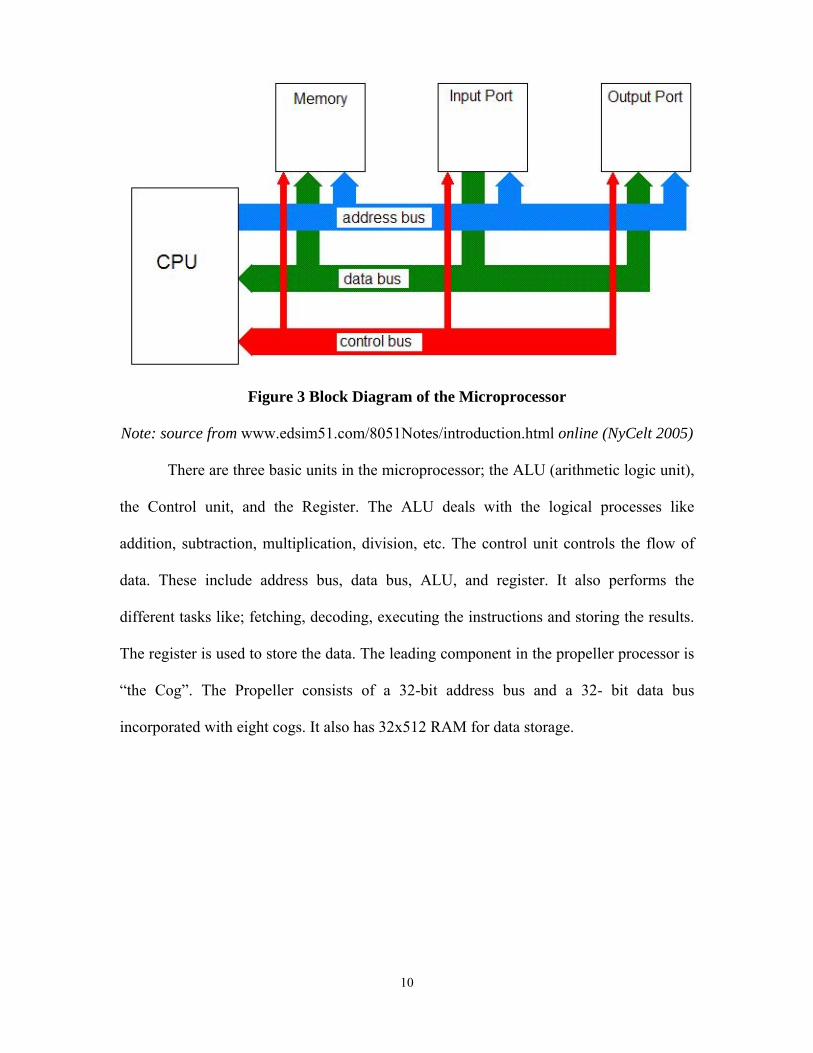
Figure 3 Block Diagram of the Microprocessor
Note: source from www.edsim51.com/8051Notes/introduction.html online (NyCelt 2005)
There are three basic units in the microprocessor; the ALU (arithmetic logic unit),
the Control unit, and the Register. The ALU deals with the logical processes like
addition, subtraction, multiplication, division, etc. The control unit controls the flow of
data. These include address bus, data bus, ALU, and register. It also performs the
different tasks like; fetching, decoding, executing the instructions and storing the results.
The register is used to store the data. The leading component in the propeller processor is
“the Cog”. The Propeller consists of a 32-bit address bus and a 32- bit data bus
incorporated with eight cogs. It also has 32x512 RAM for data storage.
10

5.2.2 Hub:
Figure 4 Block Diagram of the Central Hub
Note: source from http://www.parallax.com online (2006)
The Hub is the control unit for the entire circuit. A Bus sequencer, RAM, and ROM are
the fundamental blocks of the hub. System clock and Cog enable signals are the control
signals. Based on these two signals and system counter, the hub will point data to an
address and then write it into particular cog. System counter increments take place with
every clock signal and so the job of processing the RAM is managed by the hub. It also
allows the processor to access the system clock one at a time. This prevents it from
writing one value into two cogs. Therefore, the main purpose of the hub is to manage
shared RAM simplifying the way the processors handle different tasks. Using the hub,
one processor can also share information with other because both are sharing the same
RAM.
11
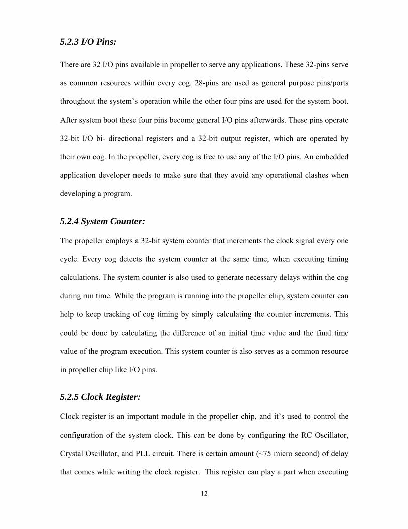
5.2.3 I/O Pins: There are 32 I/O pins available in propeller to serve any applications. These 32-pins serve
as common resources within every cog. 28-pins are used as general purpose pins/ports
throughout the system’s operation while the other four pins are used for the system boot.
After system boot these four pins become general I/O pins afterwards. These pins operate
32-bit I/O bi- directional registers and a 32-bit output register, which are operated by
their own cog. In the propeller, every cog is free to use any of the I/O pins. An embedded
application developer needs to make sure that they avoid any operational clashes when
developing a program.
5.2.4 System Counter: The propeller employs a 32-bit system counter that increments the clock signal every one
cycle. Every cog detects the system counter at the same time, when executing timing
calculations. The system counter is also used to generate necessary delays within the cog
during run time. While the program is running into the propeller chip, system counter can
help to keep tracking of cog timing by simply calculating the counter increments. This
could be done by calculating the difference of an initial time value and the final time
value of the program execution. This system counter is also serves as a common resource
in propeller chip like I/O pins.
5.2.5 Clock Register: Clock register is an important module in the propeller chip, and it’s used to control the
configuration of the system clock. This can be done by configuring the RC Oscillator,
Crystal Oscillator, and PLL circuit. There is certain amount (~75 micro second) of delay
that comes while writing the clock register. This register can play a part when executing
12
information of data according to timing calculations. The eight bit clock register has
different operations as shown in the following table.
Table 1
Clock Register Pin Structure
Bit 7 6 5 4 3 2 1 0 Operations RESET PLLENA OSCENA OSCM1 OSCM2 CLKSEL2 CLKSEL1 CLKSCL0
RESET = Reset or Reboots the entire chip.
PLLENA = Disable or Enable PLL circuit.
OSCENA = Disable or Enable Oscillator circuit.
OSCM1 & OSCM2 = Set the frequency range of Oscillator
CLKSEL2, 1 & 0 = Set the Master clock frequency and
Source of frequency (Internal/Oscillator/PLL)
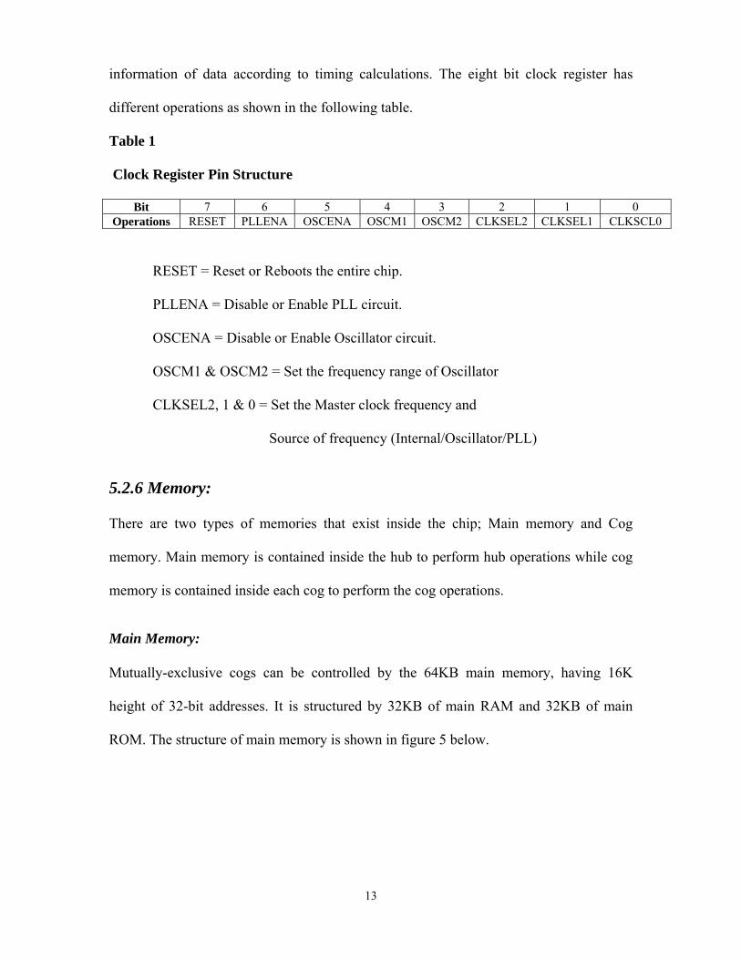
5.2.6 Memory: There are two types of memories that exist inside the chip; Main memory and Cog
memory. Main memory is contained inside the hub to perform hub operations while cog
memory is contained inside each cog to perform the cog operations.
Main Memory: Mutually-exclusive cogs can be controlled by the 64KB main memory, having 16K
height of 32-bit addresses. It is structured by 32KB of main RAM and 32KB of main
ROM. The structure of main memory is shown in figure 5 below.
13

Figure 5 Main Memory Structure
Note: source from http://www.parallax.com online (2006)
RAM: As shown in fig 5, 32KB of main RAM is available for general functionality of
the propeller chip. It can store the data from outside devices like PC’s or EEPROM
during the run time stage of operation. The first 16 addresses of the main RAM are
reserved all the time for boot loader and Interpreter operations.
ROM: The main program of the propeller chip is permanently stored in 32KB main
ROM. When starting the propeller chip for any of the applications, main ROM firmware
will provide the data needed for propeller to function. Besides this, the main ROM can
be used to store data for sine table, log table, anti-log table, and Character set.
Cog Memory: All eight cogs contain the 2KB RAM having 512 register addresses of 32-bit to process
instructions, which come from main memory. Each RAM can separately store and
execute their data. The first 16 registers are reserved as a special purpose register to
14
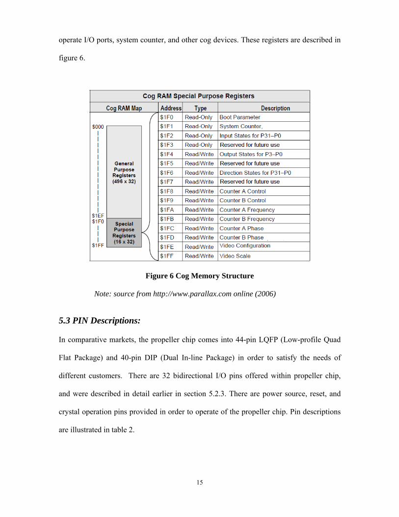
operate I/O ports, system counter, and other cog devices. These registers are described in
figure 6.
Figure 6 Cog Memory Structure
Note: source from http://www.parallax.com online (2006)
5.3 PIN Descriptions: In comparative markets, the propeller chip comes into 44-pin LQFP (Low-profile Quad
Flat Package) and 40-pin DIP (Dual In-line Package) in order to satisfy the needs of
different customers. There are 32 bidirectional I/O pins offered within propeller chip,
and were described in detail earlier in section 5.2.3. There are power source, reset, and
crystal operation pins provided in order to operate of the propeller chip. Pin descriptions
are illustrated in table 2.
15

Table 2
Pin Description of Propeller Architecture
Pin Name Direction Description
P0 – P31 I/O General Purpose I/O pins. Note: The P28 to P31 are special purpose pins during power up and reset otherwise general purpose.
VDD - Power Supply (3.3 volts) VSS - Ground BOEn I Brown Out Enable.
Note: Must be active low during run time. RESn I/O Reset pin
Note: Active low to reset the propeller chip XI I Crystal Input XO O Crystal Output
5.4 Operating Procedures:
5.4.1 Boot-up Procedure: Boot-up procedure of the propeller chip is similar to other controllers except for the 50ms
reset delay, which may arise from run-time procedure. At a start, an internal RC oscillator
will run at 20 KHz and can reach up to 12MHz once 50 ms delay is passed. By default,
the propeller chip imprints the incorporated boot loader program into cog 0 in three steps,
which are followed throughout the boot-up procedure.
1) When propeller chip starts, the boot loader seeks any external devices connected
to pin P30 and P31. If any devices are connected, the main RAM starts to fetch
and store data from it and immediately turn the chip into run-time procedure.
However, if any device is not connected to pin P30 and P31 then the boot loader
moves to step 2.
2) If any external devices are not connected, then the boot loader checks the external
EEPROM connected to pin P28 and P29 and starts fetching and storing data to the
main RAM in order to execute the program. If this process fails it moves to step 3.
16
3) If failure of the first two steps occurs, the boot loader is terminated and propeller
chip’s firmware is programmed to shut down the entire procedure.
5.4.2 Run-time Procedure: This procedure is completely under the control of the application designer. The
application designer is free to write any application code to execute propeller chip's
functionality. During the run time procedure Verilog code is loaded into cog 0 and keeps
following the applied instructions. These instructions have complete control over the
cog's functionality. These tasks can be done by observation of hub control. Execution of
Verilog code should be done in a binary form and resulting values stored into the
propeller chip’s RAM or external EEPROM. Therefore, depending on the designer,
applications are free to choose how many cogs are needed simultaneously, what pins
needed to be used, what frequency the internal clock needed to be set, and what registers
need to be configured during run-time procedure.
5.4.3 Shutdown Procedure: Shutdown procedure arises intentionally or maybe sometime accidentally. There are
certain conditions, which put the propeller into the shutdown mode. These conditions are
described as follows:
1) When VDD reaches brown-out threshold voltage around 2.7 VDC.
2) When active RESET pin is high.
3) When instructions from an application asks for a reboot procedure.
Once the shutdown procedure happens the controller may need a 50ms delay to load the
boot loader program.
17

6.0 System Design Methodology: The propeller chips, a 32-bit eight core processor, had already been designed by Parallax,
Inc. Open resources from “http://www.parallax.com” provided details about the
architecture that made it possible to understand the design and it’s inner workings. To
design the propeller architecture in Verilog, we needed to understand each module and
instruction set used. Moreover, it was necessary to create an environment that made it
possible to design this structure using Verilog.
The latest version of the Xilinx 11.1 suite was used set up the environment to
design and synthesis effective Verilog code. The Verilog is a Hardware description
language (HDL) used for implementation and verification of digital circuit designs. There
is a specific path (usually referred to as design flow) that needs to be followed in order to
design any processor using Verilog. The flow chart in fig 7 describes the path’s
implementation and the verification settings used for this design.
18
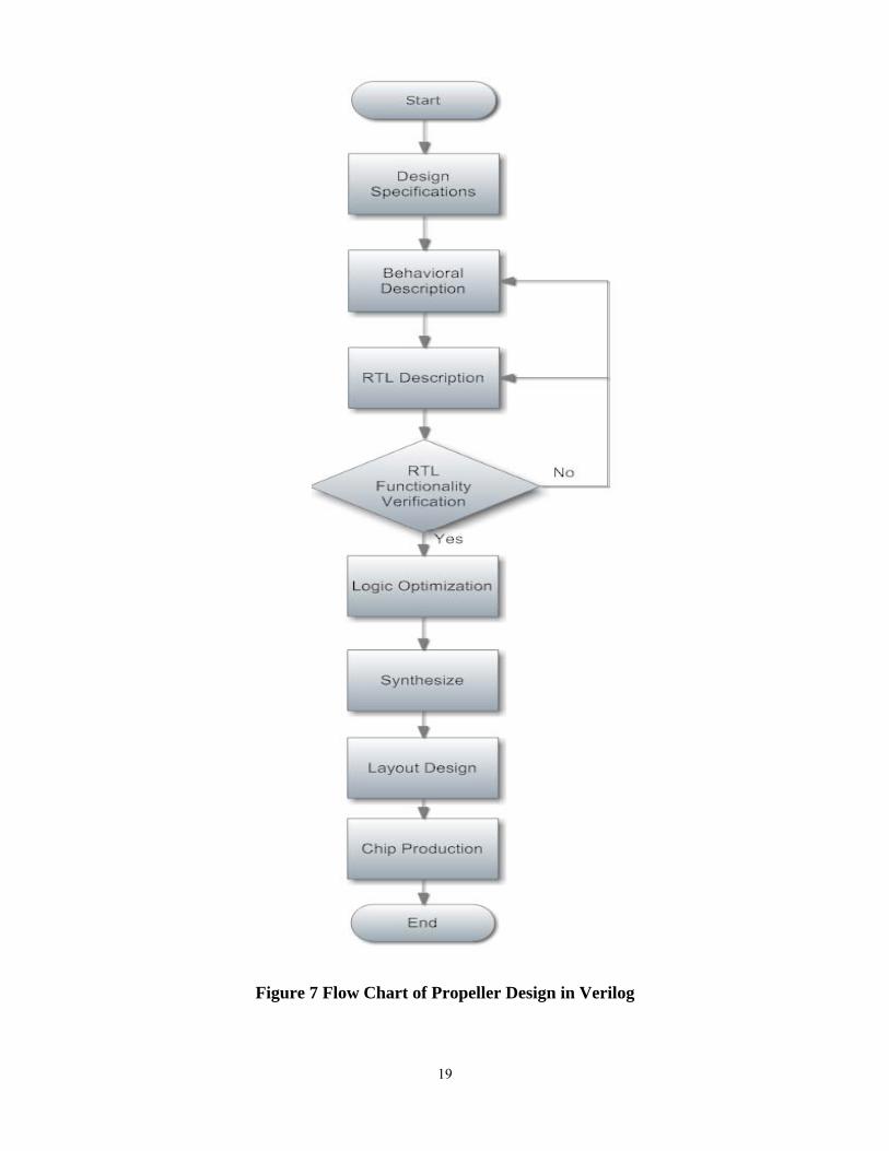
Figure 7 Flow Chart of Propeller Design in Verilog
19
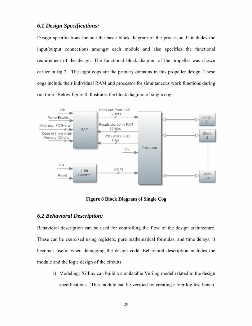
6.1 Design Specifications: Design specifications include the basic block diagram of the processor. It includes the
input/output connections amongst each module and also specifies the functional
requirement of the design. The functional block diagram of the propeller was shown
earlier in fig 2. The eight cogs are the primary domains in this propeller design. These
cogs include their individual RAM and processor for simultaneous work functions during
run time. Below figure 8 illustrates the block diagram of single cog.
Figure 8 Block Diagram of Single Cog
6.2 Behavioral Description: Behavioral description can be used for controlling the flow of the design architecture.
These can be exercised using registers, pure mathematical formulas, and time delays. It
becomes useful when debugging the design code. Behavioral description includes the
module and the logic design of the circuits.
1) Modeling: Xillinx can build a simulatable Verilog model related to the design
specifications. This module can be verified by creating a Verilog test bench.
20
In this design, a simulatable Verilog module is created for each individual
module:- for counter, RAM, and processor. Each module has their own
instructions and individual Verilog test bench. If module verification works
great then the next step is logic design of the circuit.
2) Logic design: Company engineers can build a synthesizable Verilog
description for the design. The logic design is tested by applying various “0 or
1’ combinations to the inputs and then observing the output to see if you
generated your expected combinations. This is done by creating a test bench
in same language. The output results of the logic design also come in a
waveform appearance.
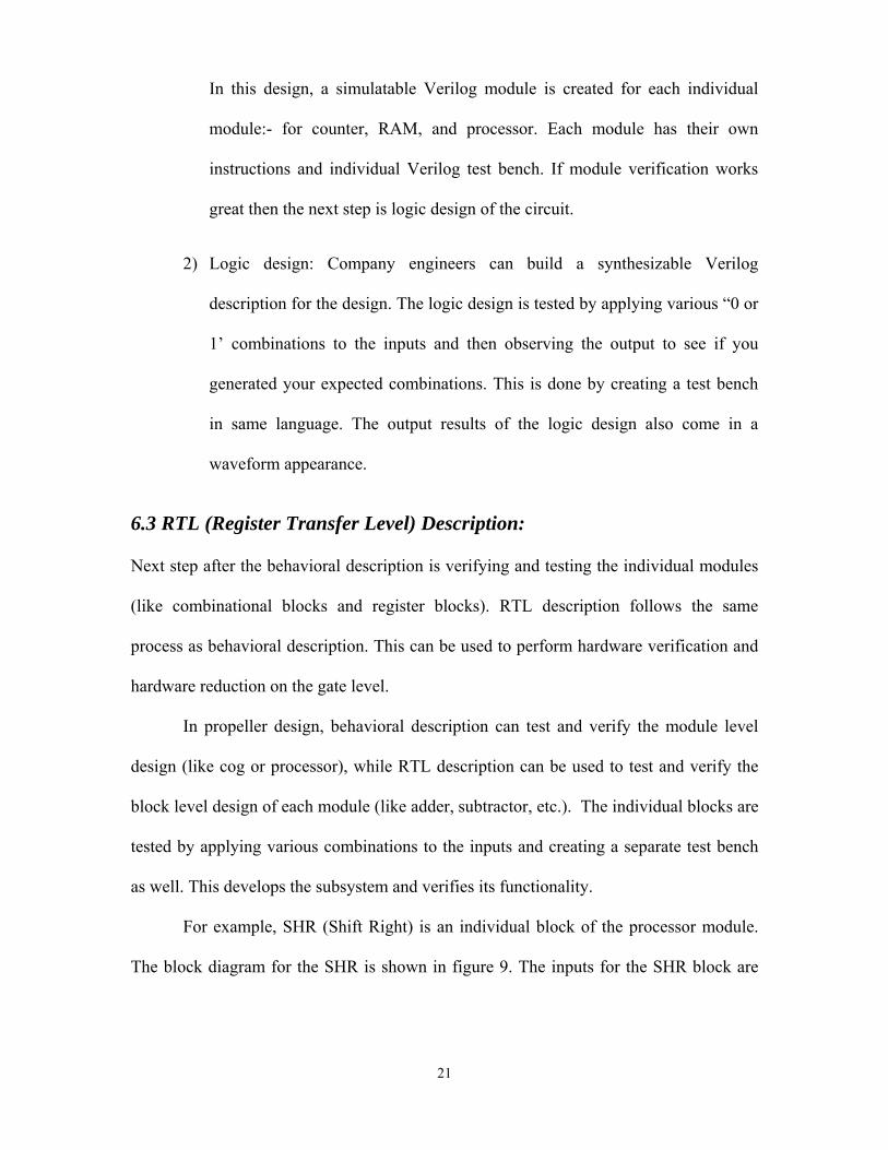
6.3 RTL (Register Transfer Level) Description: Next step after the behavioral description is verifying and testing the individual modules
(like combinational blocks and register blocks). RTL description follows the same
process as behavioral description. This can be used to perform hardware verification and
hardware reduction on the gate level.
In propeller design, behavioral description can test and verify the module level
design (like cog or processor), while RTL description can be used to test and verify the
block level design of each module (like adder, subtractor, etc.). The individual blocks are
tested by applying various combinations to the inputs and creating a separate test bench
as well. This develops the subsystem and verifies its functionality.
For example, SHR (Shift Right) is an individual block of the processor module.
The block diagram for the SHR is shown in figure 9. The inputs for the SHR block are
21
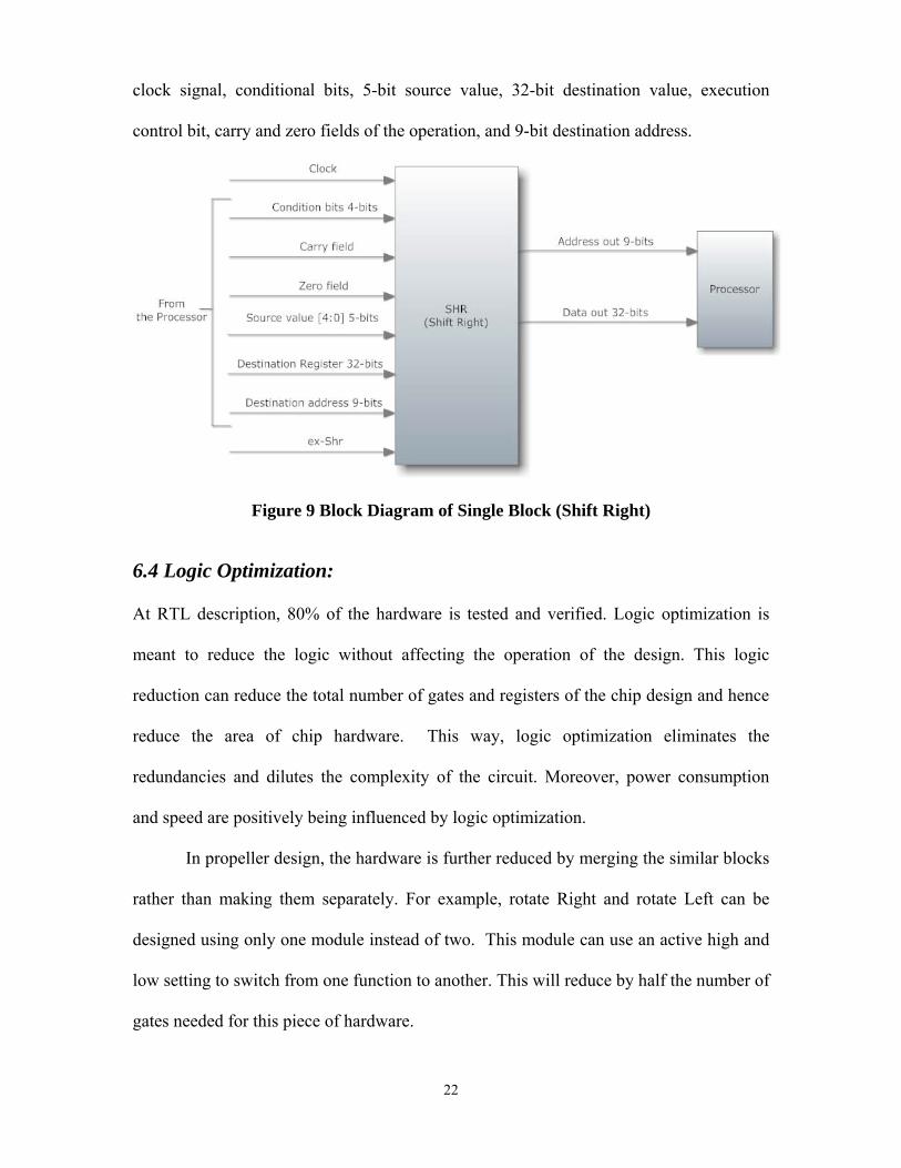
clock signal, conditional bits, 5-bit source value, 32-bit destination value, execution
control bit, carry and zero fields of the operation, and 9-bit destination address.
Figure 9 Block Diagram of Single Block (Shift Right)
6.4 Logic Optimization: At RTL description, 80% of the hardware is tested and verified. Logic optimization is
meant to reduce the logic without affecting the operation of the design. This logic
reduction can reduce the total number of gates and registers of the chip design and hence
reduce the area of chip hardware. This way, logic optimization eliminates the
redundancies and dilutes the complexity of the circuit. Moreover, power consumption
and speed are positively being influenced by logic optimization.
In propeller design, the hardware is further reduced by merging the similar blocks
rather than making them separately. For example, rotate Right and rotate Left can be
designed using only one module instead of two. This module can use an active high and
low setting to switch from one function to another. This will reduce by half the number of
gates needed for this piece of hardware.
22
6.5 Synthesize: Synthesizing a code means to obtain an actual circuit for the design. Synthesis can also be
used to optimize the design. There are various tools available in the market that can be
used to synthesize a design like Synopsis, Xilinx, etc. They generate a gate level output
of the designed blocks that need execution. Synthesizing also depicts the amount of
hardware used in the design. Synthesizing generates a report that describes the area
occupied by the number of gates and also informs the user, whether the design is feasible
to implement. For the Verilog version of the propeller, each module was synthesized
individually and then again synthesized as a whole system of modules working together.
Xilinx tool (Spartan-3E FPGA) was used as the synthesis tool.
6.6 Layout Design and Chip Production: Manufacturers use circuit design tools (like cadence) for designing the layout of a circuit.
A synthesizable design is mandatory for getting a layout design. The manufactures then
use the layout to produce make masks. These masks are then used in the actual
production of the micro-processor.
23

7.0 Economic Justification:
7.1 Executive Summary: Three engineers from San Jose State University (SJSU), has formed an Application
Specific Integrated Circuit (ASIC) design company called BSK, Inc. The first project of
this company is to design an embedded application controller with eight processors. The
architecture of the multi-core processor design is based on a similar product called
Propeller by Parallax, Inc. The Propeller chip was designed using Assembly language
and Spin programming. These two tools are not common EDA tools in the
semiconductor industry thus making the task of debugging and/or integrating other
features into the processor is difficult and expensive.
To solve this problem, the BSK propeller has designed the propeller architecture
using Verilog Hardware Description Language and C programming. These tools are
most dominant EDA design tools used in the integrated circuit industry worldwide.
Designing the propeller controller using these tools will make it more attractive to
manufacturers. These tools are cheaper and easier to work with, which will make BSK’s
designs more marketable.
The targeted customers are all the companies who buy IC designs and use those
designs to manufacture chips or make enhancements to the design (i.e. adding graphics
capability) and then manufacturing a finished product. This design will be valuable to
these customers because they will be buying a cutting edge multi-core processor that is
designed with tools that they already have been in-house. Their engineers will also
already know how to use these tools thereby avoid the need to retrain their employees.
24
This design will therefore save potential customer’s money when they use it to
manufacture their processors.
The last quarter of 2008 saw a slight drop in the number of embedded processors
sold due to a recessionary market. The overall revenue for the entire 2008 combined
was, still greater than 2007 by approximately 3.2%. This placed the market size at
around $8.3 billion worth of processors sold in 2008 in comparison to $8.1 billion in
2007. If the recession would have never happened, the numbers for 2008 would have
been even higher. This illustrates that there is a healthy market for embedded processors.
There are many competitors both big and small ranging from moms and pops
design houses to giants like Renesas Technology, Freescale Semiconductor, NEC,
Fujitsu, Atmel, NXP Semiconductor, Infineon Technology, Parallax, Inc., Texas
Instruments, etc. The goal of BSK, Inc. is to start on small base and then gradually grow
by offering more products in order to expand market share.
From the market survey, the company is going to charge a royalty fee of $1.299
for every chip sold by BSK’s customers. The company is expecting to generate a profit of
roughly $1.4 million by the end of 2014. To reach this destination, initial funding for the
first year is projected to be approximately $8.0 million and the company is expecting to
spend a total of $ 1.5 million before reaching the breakeven point.
7.2 Problem statement: The propeller processor is a multi-core processor used for embedded applications. This
particular is designed using non-standard CAD/debugging tools, which make working
with it expensive (cost of new tools/labor, etc.), and time-consuming. BSK
Incorporated’s main task is to design an architecture with similar features (eight cores)
using readily available industry standard tools making it easier to work with. This should
25

make BSK’s version of the propeller processor design more marketable as the tools used
are industry standard.
7.3 Solution and Value preposition: Main purpose of the BSK, Inc. is to design a multi-core processor to be used for
embedded applications. This will be an IP (intellectual property) firm where the finished
processor design will be sold to other companies for their various engineering projects.
BSK Incorporated is not going to do any manufacturing and thus the main business
model will revolve around designing and selling IP.
The main competitor of the company is Parallax, Inc. and BSK’s product will be
modeled to closely match their propeller processor. The major difference will be in the
type of design and debugging tools, used for the design. Parallax, Inc. uses spin,
assembly, and some C programming. Where, this company uses Verilog and C/C++
EDA tools.
A significant percentage of IC designers/manufacturers either use Verilog tools,
or have access to these tools. Therefore, this will make the design more mainstream in
contrast to the Parallax’s design, which might require hard to finding expertise/expensive
(spin and Assembly engineers). Also the purchase of the above mentioned tools, since
they are not frequently used by most companies, will add an extra cost on their design
budgets if they go with Parallax’s processor.
7.4 Market size: According to PCWorld news, semiconductor market fell down by 3.2% in the last quarter
of 2008. Despite lower revenue in this last quarter, total annual revenue of the embedded
processor market in 2008 was still higher than the total annual revenue in 2007.
26

Customers spent approximately $8.3billion which slightly surpassed the $8.1 billion
spent in 2007.
Another report courtesy of EE times India clearly illustrates the upwards revenue
trend that embedded processors are enjoying. They forecasted that the projected revenue
growth will reach $14.2 billion by 2013. Microprocessor market has so far grown by
8.3% during this recessionary period. This strong demand is being driven by the
increasing popularity of embedded chips in consumer and commercial electronics. Most
of these systems require high computing capability while consuming low power. The
BSK propeller chip is designed to meet these requirements.
Considering the requirements of the multi-core multiprocessor in the current
market, the Propeller chip will have a multi-core microprocessor with real time output.
Processor trends show that due to limitations in Moore’s law, the number of transistors in
a processor will slow down significantly in the coming years. This means that to improve
performance, processors will have an increasing number of “cores” in order to
significantly increase computing power. From this view point, an octal-core embedded
processor is sure to capture the needs of potential customers, and thus BSK, Inc. will grab
a small piece of market share in near future. Figure 10 shows details of the micro
component market. In this figure, MPUs (microprocessors), MCUs (microcontrollers)
and DSPs (Digital Signal Processors) are also included since they are widely used inside
micro components.
27
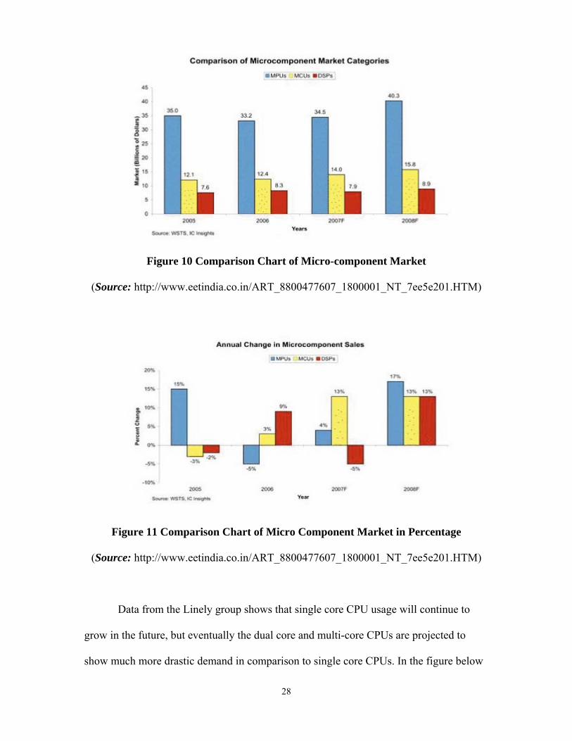
Figure 10 Comparison Chart of Micro-component Market
(Source: http://www.eetindia.co.in/ART_8800477607_1800001_NT_7ee5e201.HTM)
Figure 11 Comparison Chart of Micro Component Market in Percentage
(Source: http://www.eetindia.co.in/ART_8800477607_1800001_NT_7ee5e201.HTM)
Data from the Linely group shows that single core CPU usage will continue to
grow in the future, but eventually the dual core and multi-core CPUs are projected to
show much more drastic demand in comparison to single core CPUs. In the figure below
28
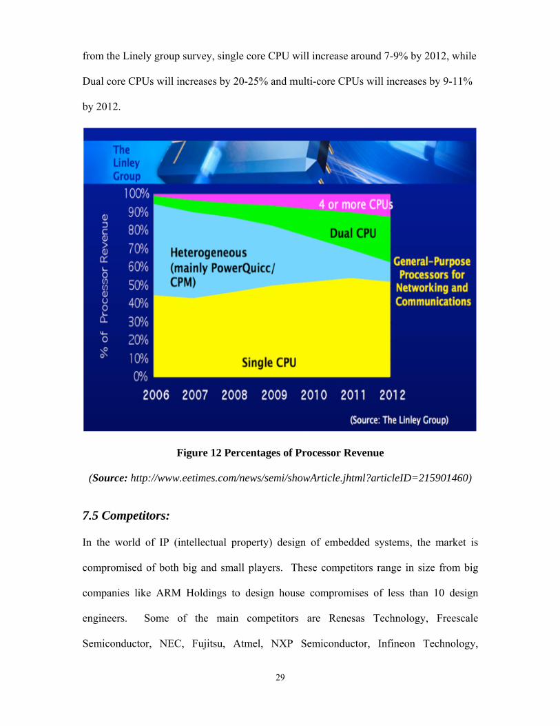
from the Linely group survey, single core CPU will increase around 7-9% by 2012, while
Dual core CPUs will increases by 20-25% and multi-core CPUs will increases by 9-11%
by 2012.
Figure 12 Percentages of Processor Revenue
(Source: http://www.eetimes.com/news/semi/showArticle.jhtml?articleID=215901460)
7.5 Competitors: In the world of IP (intellectual property) design of embedded systems, the market is
compromised of both big and small players. These competitors range in size from big
companies like ARM Holdings to design house compromises of less than 10 design
engineers. Some of the main competitors are Renesas Technology, Freescale
Semiconductor, NEC, Fujitsu, Atmel, NXP Semiconductor, Infineon Technology,
29

Parallax, Inc., Texas Instruments, etc. The Embedded Controller markets in 2008 are
shown in figure 13.
Figure 13 Competitive Embedded Controller Market in Year 2008
(Source: http://www.eetasia.com/ART_8800570077_1034362_NT_9b19f76b.HTM)
The goal of the company is to start off getting a share of the small moms & pops
design houses. After establishing a small business, the company has a plan on making
bigger designs that will compete with the architectures such as ARM, MIPS, X-scale, and
x86.
7.6 Customers: Embedded systems processors are used in applications ranging from Robotics, control
solutions, communications, and digital systems processing just to name a few. The
30

company intends to market IP designs to potential customers in all the above stated fields
in order to maximize customer base and increase growth potential.
Initial target of the BSK, Inc. is those companies that make chips for robotics
applications including; Motoman Robots, Fanuc Robots, Panasonic Robots, OTC Robots,
Nachi Robots, ABB, Robots, Kuka Robots, etc.
The embedded control side, the company will target; Intel, Beyond
Semiconductor, Bright Scale, Maxwell Technologies, agile Systems, AMD, GE, Funuc
Embedded Systems, etc.
Communication companies are an ever growing customer for embedded with the
continued explosion of cell phones and their propensity to get obsolete in a very short
period of time. Some of company’s potential customers in this segment are: Averlogic,
Cirrus Logic, Customer Microcircuits Limited, Rensas Technology, Holtek
Semiconductor, IBM, HP, Marwell Technology, Mitsubissi Semiconductor, Motorola,
Panasonic, Semtech, Nokia, etc.
7.7 Cost Summary: BSK Incorporated only design and sells their IP but does not do any actual
manufacturing. There is no manufacturing division included when building the company.
In the cost summary, the company includes fixed costs and estimated variable costs
depending on the IP design sells.
7.7.1 Fixed Cost: The company has decided to include establishment costs (licensing costs for electronics
design tools, computer equipments and stationary costs, and furniture costs), office rent,
light bill, maintenance costs, bank interest, IP design patent costs, and salary of
31

employees in fixed costs. Future forecast for fixed costs up to five years is shown in table
3.
Table 3
Fixed Costs
Expenses 2009 2010 2011 2012 2013 Licensing cost from Xilinx (Design Tool) $40000 $0 $0 $0 $0
Licensing Cost from Synopsis (Debugging Tool) $40000 $0 $0 $0 $0
Licensing Cost from Linux (Operating System) $12000 $0 $0 $0 $0
Office Rent $60000 $80000 $120000 $180000 $240000 Furniture Cost $6000 $2000 $2000 $3000 $2000 Computer Equipment and Stationary $22000 $0 $30000 $0 $50000
Total PG&E Bill $3000 $6600 $7200 $8400 $12000 Maintenance $1500 $1500 $1500 $1500 $1500 Telephone, Internet, and Fax Bills $2000 $2000 $3500 $3500 $4500
Bank Interest $20000 $20000 $20000 $20000 $20000 Patent Cost $500 $20000 $0 $0 $0 Salary $240000 $346000 $675000 $1010000 $1345000TOTAL $446500 $478100 $859200 $1226400 $1675000
7.7.2 Employee Wages: In fixed costs the company includes competitive employment wages. Employment wages
are decided based on the position and experience to work with the company. Estimated
employment wages are described in table 4.
32

Table 4
Employment Wages
Department 2009 2010 2011 2012 2013 MANAGEMENT
CEO $80000 $90000 $105000 $120000 $140000 Project Manager - - $65000 $70000 $140000(2)*Director of Operations - - - $65000 70000
ENGINEERING CTO $80000 $90000 $105000 $120000 $140000 Senior Engineer - - $65000 $135000(2)* $145000(2)*Junior Engineer - - - $50000 $105000(2)*
SALES AND MARKETING VP of Marketing $80000 $90000 $105000 $120000 $140000 Sales Manager - - $65000 $70000 $75000 Business Analyst - - - $40000 $45000 Sales and Marketing Assistant - - - - $50000
HUMAN RESOURCE Customer Service Lead - $38000 $45000 $50000 $55000 Customer Service Assistant - - - $40000 $45000 Staffing Supervisor - - - - $50000
FINANCE Finance Manager - - $75000 $80000 $90000 General Accounting - $38000 $45000 $50000 $55000
Note: (2)* = two employs
Figure 14 Comparative Salaries
33

7.7.3 Variable Cost:
advertisement costs, contract employee costs, and customer
rvice costs as variable costs. These costs are estimated depending on how many IP’s
are sold or projected to sell. In this competitive market, the company has decided to use
2% of the fixed costs for advertisement of the product. Table 5 describes the variable
costs for near future.
Table 5
Variable Costs
The company considers
se
Category 2009 2010 2011 2012 2013 Advertisement 0 $9652 $17184 $24528 $33500 Contract employee $4000 0 $4500 $5500 $7000 Customer service $10000 0 $15000 $20000 $25000 Total 0 $23652 $36684 $50028 $65500
Figure 15 Estimation of Variable Cost
Above figure illustrates the variable cost increases with increasing designed IP sells.
34

7.8 Price Point:
The company determined price point by directly getting price quotes from other
ompanies selling similar designs. The company first pretended to be a startup chip
design and manufacturing company based in China. “Marketing” then called various
design houses (big and small) including the likes of ARM & MIPS and expressed interest
in buying IP designs of their various chips. BSK, Inc. wanted to know the amount of
royalty charged if it used their various designs to manufacture processors for embedded
system processors. The prices ranged from $0.50 ~ $3.99 depending on the complexity,
computing power and the features of the design. Therefore, the price point was
determined by investigation/analysis of the price range that potential customers are
paying for royalty on similar items to the other companies. After analysis, marketing
personnel decided to set the royalty fee at $1.299 for every chip sold. Analysis from the
marketing and sales department shows that potential customers are willing to pay this
amount or more for designs with fewer computing power than what this company intends
to design.
Assessment: Market analysis was used to determine a qualitative SWOT assessment. In the huge
mbedded microcontroller market, new technologies never end. The company realizes the
challenges of a competitive market. This led to the design of a user friendly eight core
processor. In spite of this, any start up company has to struggle to gain customers in this
recession.
By increasing the needs of embedded products, BSK is offering a product that it
feels confident will help the company break into new markets worldwide. Below is a
c
7.9 SWOT
e
35
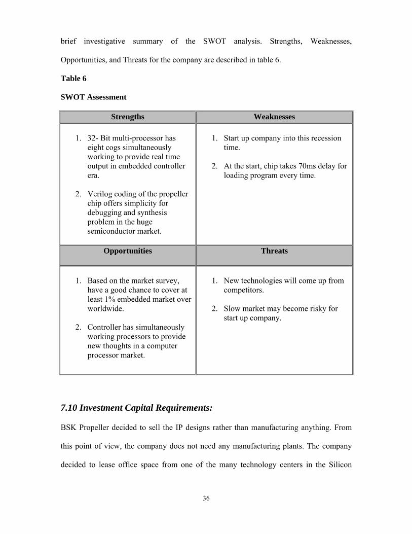
brief investigative summary of the SWOT analysis. Strengths, Weaknesses,
Opportunities, and Threats for the company are described in table 6.
Table 6
SWOT Assessment
Strengths Weaknesses
1. 32- Bit multi-processor has eight cogs simultaneously working to provide real time utput in embedded controller
r
gging and synthesis roblem in the huge
1. Start up company into this recession
time.
2. At the start, chip takes 70ms delay for oera.
2. Verilog coding of the propellechip offers simplicity for debupsemiconductor market.
loading program every time.
Opportunities Threats
1. Based on the market survey,
have a good chance to cover at least 1% embedded market over worldwide.
s in a computer processor market.
1. New technologies will come up from
competitor
2. Slow market may become risky for
2. Controller has simultaneously working processors to provide new thought
s.
start up company.
7.10 Investment Capital Requirements:
BSK Propeller decided to sell the IP designs rather than manufacturing anything. From
any manufacturing plants. The company
decided to lease office space from one of the many technology centers in the Silicon
this point of view, the company does not need
36
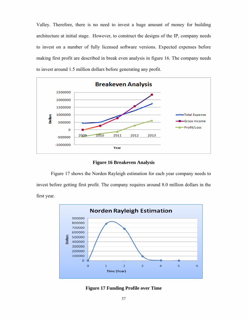
Valley. Therefore, there is no need to invest a huge amount of money for building
architecture at initial stage. However, to construct the designs of the IP, company needs
to invest on a number of fully licensed software versions. Expected expenses before
making first profit are described in break even analysis in figure 16. The company needs
to invest around 1.5 million dollars before generating any profit.
Figure 16 Breakeven Analysis
Figure 17 shows the Norden Rayleigh estimation for each year company needs to
invest before getting first profit. The company requires around 8.0 million dollars in the
first year.
Figure 17 Funding Profile over Time
37

7.11 Personnel: The co-founders will be receiving guidance/mentoring from experienced SJSU advisors.
Considering technical and management advice from mentors, the company decided to
divide their departments into five major groups: management, engineering, sales and
marketing, human resource, and finance. Each group is staffed with necessary team
members as described in table 7.
Table 7
Department Allocation
Department 2009 2010 2011 2012 2013 Management 1 1 2 3 4 Engineering 1 1 2 4 5 Sales and Marketing 1 1 2 3 4 Human Resource 0 1 1 2 3 Finance 0 1 2 2 2 Total 3 5 9 14 18
The company has decided to reach customers by hiring a proven marketing team.
The importance of the sales and marketing group is about to be same as that of
ent and engineering. Table 4 presents the comparative employment wages up to
7.12 Business and Revenue Model: BSK Incorporated Design Comp y is a uniq company i this segment by providing a
breakthrough eight core process design. Th ompany’s rketing team has developed
o sell the IP designs and c arge ~$1.29 r every ch sold.
achieving this goal. This team plans to use advertisement in technical news papers,
managem
five years.
an ue n
or e c ma
a plan t h fo ip
The company has intends to sell about 1 million IP designs by 2012 which is
~0.20% (fraction of 1%) market share. The marketing and sales teams are committed to
38

technical social networking sites/forums, magazines, and representation in technical
conferences. Table 8 illustrates projected business and revenue model of the company for
five years.
able 8
Business and Revenue Model
T
2009 2010 2011 2012 2013 Price per IP Unit $1.299 $1.299 $1.299 $1.299 $1.299 # of Units Sold 0 200000 600000 1200000 1800000 IP Revenue 0 $259800 $779400 $1558800 $2338200 Total Expenses $446500 $501752 $895884 $1276428 $1740500
7.13 Strategic Alliance/Partners:
In order to position the company on firm ground, BSK Inc. reached out to Parallax and
offer to redes
ign their other architectures using Verilog. BSK, Inc. requested to have
riety source codes for these architectures. In exchange BSK will get ~30% of
edesigned chips are sold (30% of $1.29≈0.38).
The benefit for Parallax is they will be able to reach custom at they ad
ecaus ols. They will als des e
o hire s. The benefit for BSK will
e gaining access to Parallax customers and designs since they are already an established
million
their prop
the royalty amount when these r
ers th never h
access to before b e of their choice of to o get there ign remad
without having t new ngineers or investing in new tool e
b
company.
7.14 Profit & Loss:
Estimated expenses and sales are evaluated in the profit and loss statement. The
company’s expenses are calculated in cost the summary statement and they include fixed
costs and predicted variable costs. The company will spend approximately $1.5
39

dollars before generating any profit. Norden Rayleigh’s estimation in fig 18 illustrates the
spending profile and hence to keep tracking on financial flow of the company.
Figure 18 Cumulative Funding over Time
Return on Investment (ROI) graph in figure 19 shows profit, loss and expenses of
the company. The formula for Return on investment is:
% ROI = [(Total Income – Total Expense)/Total Expense] x 100
Figure 19 Returns on Investment (%)
40

Figu ncome and
total expenses of the respected year.
re 20 presents the profit/loss for every year by taking the total i
Figure 20 Yearly Distribution of Profit/Loss
The company generates their profit/loss statement each quarter to demonstrate the
financial performance. Table 9 demonstrates the profit/loss for Q3’09 to Q2’10. During
these quarters, this start up company invested the first round of funds from the bank.
Table 9
Business Revenue Model for Q3’09 to Q2’10
Total Expected IP sell for Royalty
Revenue Fixed Variable Total Cost= Profit/Lossfrom Royalty
(in $)
Cost (in $)
Cost F.C. + V.C. (in $) (in $) (in $)
Q3’09 0 0 223250 0 223250 -223250 Q4’09 0 0 223250 0 223250 -223250 Q1’10 3000 4255 -85285 0 38970 119525 4730 12Q2’10 30000 38970 119525 4730 124255 -85285
41
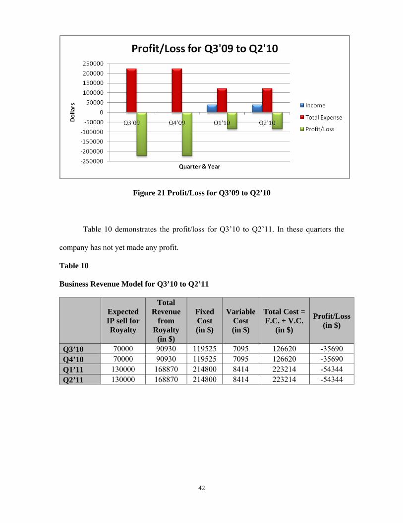
Figure 21 Profit/Loss for Q3’09 to Q2’10
Table 10 demonstrates the profit/loss for Q3’10 to Q2’11. In these quarters the
company has not yet made any profit.
Table 10
Business Revenue Model for Q3’10 to Q2’11
Total Expected IP sell for Royalty
Revenue Fixed Variable Total Cost = Profit/Loss from Royalty
(in $)
Cost (in $)
Cost F.C. + V.C. (in $) (in $) (in $)
Q3’10 70000 90930 119525 7095 126620 -35690 Q4’10 70000 90930 119525 7095 126620 -35690 Q1’11 130000 168870 214800 8414 223214 -54344 Q2’11 130000 168870 214800 8414 223214 -54344
42

Figure 22 Profit/Loss for Q3’10 to Q2’11
Table 11 demonstrates the profit/loss for Q3’11 to Q2’12. These quarters devote a
piece of cake to the company. The company starts making a profit in Q1 of year 2012.
Table 11
Business Revenue Model for Q3’11 to Q2’12
Expected IP sell for Royalty
Total Revenue
from Royalty
Fixed Cost (in $)
Variable Cost (in $)
Total Cost= F.C. + V.C.
(in $)
Profit/Loss(in $)
(in $) 170000 220830 214800 9928 224728 -3898 Q3’11
Q4’11 170000 220830 214800 9928 224728 -3898 Q1’12 250000 324750 306600 11256 317856 6894 Q2’12 250000 324750 306600 11256 317856 6894
43
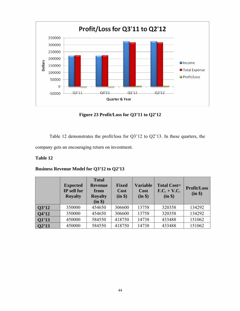
Figure 23 Profit/Loss for Q3’11 to Q2’12
Table 12 demonstrates the profit/los
compan
evenue Model for Q3’12 to Q2’13
s for Q3’12 to Q2’13. In these quarters, the
y gets an encouraging return on investment.
Table 12
Business R
Total Expected IP sell for Royalty
Revenue Fixed Variable Total Cost= Profit/Lossfrom Royalty
(in $)
Cost (in $)
Cost F.C. + V.C. (in $) (in $) (in $)
Q3’12 3 320358 134292 350000 454650 06600 13758 Q4’12 350000 454650 306600 13758 320358 134292 Q1’13 450000 584550 418750 14738 433488 151062 Q2’13 450000 584550 418750 14738 433488 151062
44
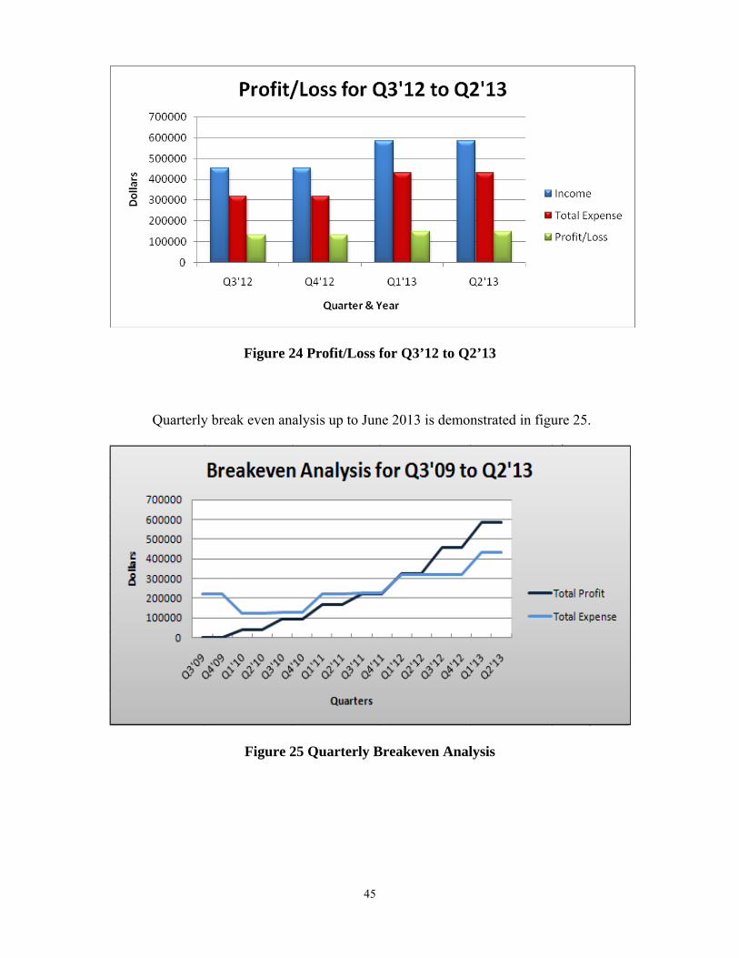
Figure 24 Profit/Loss for Q3’12 to Q2’13
Quarterly break even analysis up to June 2013 is demonstrated in figure 25.
Figure 25 Quarterly Breakeven Analysis
45

7.15 Exit Strategy: The stakeholders at BSK Inc. include three founders and two different venture capital
firms. The stakeholders have decided that in the near future the company will go public
depending on its rate of growth and market conditions. The alternate exit strategy is to
sell the company to a more established rival in the event that they make an offer that BSK
stakeholders cannot refuse.
This being said the soft market brought about by the housing and credit crisis are
slowly improving. BSK, Inc. also foresees a steady growth in revenue and company size
because technology companies have been fairing decently within that past 2 quarters of
2009. The goal is to do a thorough evaluation of the BSK Inc. balance sheet and overall
market conditions in approximately the fourth quarter of 2014. The outcome of this
analysis will determine if the company goes public, gets acquired by another company or
remains privately held.
46

8.0 Project Schedule:
The project schedules for final project implementations shown in figure 26.
Figure 26 Project Schedule for ENGR 298
47
9.0 Conclusion:
Three SJSU engineering students formed a company called BSK Propeller Inc. and set to
design an eight-core embedded process using standardized electronic design tools. After
researching, reading, writing and testing code, debugging designs, and asking and
receiving help, this company has finished designing an eight-core processor. Using
Verilog to design an eight core was made easier by the fact that there were an abundance
of materials and instructions on how to design using Verilog. This is because it is a
standard tool. With the verification of a working design, the company is ready to start
marketing its first design. According to break even analysis, BSK Propeller Inc. should
start being profitable from the first quarter of year 2012. Given the success of the design,
the company anticipates that propeller multi-core controller designed using Verilog will
be successful in the market.
48
10.0 Future Work: Future designs include a processor modified with 16 cogs that will perform tasks up to
four times faster than our current design. This job is more complicated and time
consuming than the present design. This future design will run each cog at 160 MIPS
(Million Instructions per Second) and increase clock speed up to 160 MHz.
The present architecture is designed using a four stage pipeline concept. If
successful, this design with full pipelining capability will quadruple the propeller speed.
49
11.0 References: Abu A., I. M. (2004). Evalution of Application Specific Multiprocessor Mobile System. Florida: Department of Computer science and Engineering, Florida Atlantic University. Advanced Micro Devices. (2005). MULTI-CORE PROCESSORS—THE NEXT EVOLUTION IN COMPUTING. Retrieved October 2, 2009, from AMD: http://multicore.amd.com/Resources/33211A_Multi-Core_WP_en.pdf Benoliel, I. (2002, May 27). How to Calculate Your Breakeven Point . Retrieved October
15, 2009, from Entreprenur: http://www.entrepreneur.com/money/moneymanagement/financialmanagementcolumnistpamnewman/article52102.html
Centrell, T. (2006). Mind Mannered Propeller Processor. 80-84. Clarke, P. (2008, March 3). Actual data show January chip sales fell on annual basis.
Retrieved November 15, 2009, from EE Times: http://www.eetimes.com/showArticle.jhtml?articleID=206901795
Davey, M. (2008, March 3). Parallax Propeller Chip Overview. Retrieved October 25, 2009, from Chibots: http://www.chibots.org/?q=node/463 Electronic News. (2008, December 8). Multi-core MPU market to skyrocket, iSuppli says.
Retrieved November 16, 2009, from Electronicsweekly: http://www.electronicsweekly.com/Articles/2005/12/08/37147/Multi-core-MPU-market-to-skyrocket-iSuppli-says.htm
Electronics.ca Research Network. (2009, March 29). Embedded Processors Top 10
Billion Units in 2008. Retrieved November 28, 2009, from Electronics.cs publications: http://www.electronics.ca/presscenter/articles/1078/1/Embedded-Processors-Top-10-Billion-Units-in-2008/Page1.html
Fiveash, K. (2008, February 26). EU throws €5.5bn at embedded chips and nanotech.
Retrieved November 15, 2009, from The register: http://www.theregister.co.uk/2008/02/26/eu_joint_technology_initiatives/
Gaudin, S. (2008, November 19). Analysts Predict Global Drop in 2008 Chip Sales.
Retrieved October 25, 2009, from PCWorld: http://www.pcworld.com/businesscenter/article/154186/analysts_predict_global_drop_in_2008_chip_sales.html
Harrison, D. M. (2005, Faburary 19). Microprocessor Interfacing Techniques. Retrieved
October 15, 2009, from UPSCALE: http://www.upscale.utoronto.ca/ Holland, C. (2008, October 14). Market for MCUs, eMPUs and DSPs to reach $8.6B .
50
Retrieved October 28, 2009, from EE India Times: http://www.eetindia.co.in/ART_8800547831_1800001_NT_48e47d8a.HTM
Inc., P. (2008). Propeller Information. Retrieved August 24, 2009, from Parallax:
http://www.parallax.com/tabid/407/Default.aspx Intel. (2009). Intel® System Controller Hub US15W. Retrieved September 26, 2009, from
Intel: http://download.intel.com/design/chipsets/embedded/prodbrf/319545.pdf Ledger, J. (2007). The Propeller cook book (Vol. 1.4). Propeller Protoboard
Experimenter Designs. Merritt, R. (2009, March 20). Multicore CPUs face slow road in comms. Retrieved
October 31, 2009, from EETimes: http://www.eetimes.com/news/semi/showArticle.jhtml?articleID=215901460
Merritt, R. (2009, March 17). Tool puts parallelism in embedded code. Retrieved October
31, 2009, from EETimes: http://www.eetimes.com/showArticle.jhtml;jsessionid=P05OCMTDWOICEQSNDLOSKH0CJUNN2JVN;?articleID=215900594
Microcomponents shows mixed market conditions . (2007, August 29). Retrieved
November 15, 2009, from EE Times India: http://www.eetindia.co.in/ART_8800477607_1800001_NT_7ee5e201.HTM
Niccolai, J. (2008, December 16). Chipmakers face longest decline in history, Gartner
says. Retrieved November 3, 2009, from InfoWorld: http://www.infoworld.com/t/hardware/chipmakers-face-longest-decline-in-history-gartner-says-664
Nollet, R. T. (n.d.). The new Propeller Chip from Parallax. Retrieved November 2, 2009
, from R. T. Nollat Austrilia: http://www.nollet.com.au/propeller.htm Palnitkar, S. (1996). Verilog HDL: A guide to Digital Design and Synthesis. SunSoft
Press. Parallax Propeller. (2006, July 7). Retrieved August 24, 2009, from Parallax:
http://www.parallax.com/Portals/0/Downloads/docs/prod/prop/PchipBlockDiagramRevA-0109.pdf
Parallax Propeller. (2006). Retrieved August 24, 2009, from Wekipedia:
http://en.wikipedia.org/wiki/Parallax_Propeller Parallax Propeller. (2009). Retrieved October 26, 2009, from Ray's Logic:
http://rayslogic.com/propeller/propeller.htm Parallax. (2006). Propeller Eduction Kit Labs: Fundamentals. Rocklin: Parallax.
51

Parametric Product Table. (n.d.). Retrieved October 25, 2009, from Atmel: http://www.atmel.com/dyn/products/param_table.asp?family_id=607&OrderBy=part_no&
Ravi S., R. A. (2006, September). Application Specific Heterogeneous Multiprocessor
Synthesis Using Extensible Processors. Integrated Circuit Design and System , 5, pp. 1581-1601.
Savage, C. (2008). PROPELLER MULTI-CONTROLLER. Retrieved September 25, 2009
, from Parallax: http://www.parallax.com/Resources/ParallaxProjects/Propeller/tabid/664/Default.aspx
Wikipedia. (2009). Microprocessor. Retrieved September 15, 2009, from Wikipedia:
http://en.wikipedia.org/wiki/Microprocessor Wikipedia. (2009). Multi-core. Retrieved August 25, 2009, from Wikipedia:
http://en.wikipedia.org/wiki/Multi-core_%28computing%29 Wong, W. (2006, August 21). EiED Online>> Parallax Propeller. Retrieved October 15
, 2009, from Electronic design: http://electronicdesign.com/Articles/Index.cfm?AD=1&AD=1&AD=1&ArticleID=13329
EE TImes Asia. (2009, April 17). Microchip seeks to 'elbow out' MCU rivals. Retrieved
November 25, 2009, from EE Times Asia: http://www.eetasia.com/ART_8800570077_1034362_NT_9b19f76b.HTM
NyCelt LLC. (2005-2006). The 8051. Retrieved November 25, 2009, from Edsim51:
http://www.edsim51.com/8051Notes/introduction.html
52

Appendix A Set up the Xilinx 11.1 suit environment and update it:
1. Go to the website
www.xilinx.com/support/download/index.htm
2. Select first option from Download Design Tools.
3. Creat an account in Xilinx.
4. Open the link on your email ID emailed by Xilinx after registration.
5. Download the Xilinx ISE 11.1 suit and extrect the zip file.
6. Run set-up file and select ISE wabepack to install.
7. Update the software by selecting help teb on Xilinx 11.1 suit and click on the
Xilinx update. This can update Xilinx 11.3 suit version.
53

Appendix B
Create a project in Xilinx suit:
1. Open updated Xilinx tool.
2. Create new project.
3. Select the Verilog module and specify the file name with any any extension.
4. Declare the input and output if u want to declare if before the coding starts.
Remember, you can do it lateron aslo.
5. After finishing declaring I/O, Start writing verilog code.
6. Make an test bench to test your code using create new source and just select
verilog test bench this time instead of verilog module.
7. Run the behaviour description of the main code and solve the errors indicated.
54

Appendix C Main Processor code in Verilog:
`timescale 1ns / 1ps ////////////////////////////////////////////////////////////////////////////////// // Company: // Engineer: // // Create Date: 01:54:25 11/17/2009 // Design Name: // Module Name: cog // Project Name: // Target Devices: // Tool versions: // Description: // // Dependencies: // // Revision: // Revision 0.01 - File Created // Additional Comments: // ////////////////////////////////////////////////////////////////////////////////// module cog (I_out,clock,reset); output [31:0] I_out; input clock,reset; reg [31:0] I_out; reg [31:0] IR,dvalue,svalue,R3; reg [8:0] PC; reg [5:0] operation,op; reg z,c,r,i,dbit,sbit,result,z1,c1,C_flag,Z_flag,v; reg exjmp,exadd,exmuxnz,exmuxz,exmuxnc,exror,exrol,exshr,exshl,exsar,exrev,exmovs,exmovd,exmovi,exOR,exEXOR,exmuxc,exmins,exrcr,exrcl,exmaxs,exmin,exmax,extest,extestn; reg wbjmp,wbadd,wbmuxnz,wbmuxz,wbmuxnc,wbror,wbrol,wbshr,wbshl,wbsar,wbrev,wbmovs,wbmovd,wbmovi,wbOR,wbEXOR,wbmins,wbmuxc,wbrcr,wbrcl,wbmaxs,wbmin,wbmax,wbtest,wbtestn;
55
reg [3:0] condition; reg [8:0] sourceadd,destadd,source1,dvalue2,dvalue3; reg [4:0] source; reg [22:0] dvalue1,dvalue4; reg [31:0] data [0:511]; wire [1:0] count; wire [8:0] Rsource,jmpaddress,addaddress,muxnzaddress,muxzaddress,muxncaddress,muxcaddress,roladdress,roraddress,minaddress,maxaddress,maxsaddress,ORaddress,EXORaddress,testaddress,testnaddress,shraddress,shladdress,saraddress,revaddress,movsaddress,movdaddress,moviaddress,minsaddress,rcraddress,rcladdress; wire Zjmp,Zadd,Padd,Zmins,Gmins,Zmaxs,Gmaxs,Zmin,Gmin,Zmax,Gmax,Ztest,Ptest,Ztestn,Ptestn,ZOR,POR,ZEXOR,Pmuxz,Zmuxz,PEXOR,Pmuxc,Zmuxc,Pmuxnc,Zmuxnc,Pmuxnz,Zmuxnz; wire [31:0] Rdest,Rjmp,Radd,Rmuxnz,Rmuxnc,Rror,Rrol,Rshr,Rshl,Rsar,Rrev,Rmovs,Rmovd,Rmovi,Rmins,Rrcr,Rrcl,Rmaxs,Rmin,Rmax,Rtest,Rmuxz,Rtestn,Ror,Rexor,Rmuxc; initial begin $readmemh ("in_file.txt",data); end initial begin PC = 9'h000; C_flag = 1'b0; Z_flag = 1'b0; v = 1'b1; end //RAM r0 (data_out,dataout,clock,we,I_in,re,raddress); counter0 c0 (count,clock,reset); // FETCH THE INSTRUCTION IN R1 always @ (posedge clock)begin if (count == 2'b11)begin IR= data[PC]; if (v == 1'b1)begin PC = PC +1; end end
56

end // DECODE THE INSTRUCTION IN R1 always @ (posedge clock)begin if (count == 2'b00)begin operation = IR [31:26]; condition = IR [21:18]; sourceadd = IR [8:0]; destadd = IR [17:9]; c = IR [24]; z = IR [25]; r = IR [23]; i = IR [22]; end end // SET THE CONTROL BITS TO FETCH THE DESTINATION VALUE always @ (posedge clock)begin if (count == 2'b10)begin dbit = 1'b0; end else if (count == 2'b00)begin dbit = 1'b1; end end // FETCH THE DESTINATION VALUE AND STORE IN THE REGISTER always @ (posedge clock)begin if (count ==2'b01)begin if (dbit == 1'b1)begin dvalue = data[destadd]; dvalue1 = dvalue [31:9]; dvalue2 = dvalue [31:23]; dvalue3 = dvalue [8:0]; dvalue4 = dvalue [22:0]; end end end // SET THE CONTROL BIT TO FETCH THE SOURCE VALUE always @ (posedge clock)begin if (count == 2'b01)begin sbit=1'b1; end else if (count == 2'b11)begin
57
sbit = 1'b0; end end // FETCH THE SOURCE VALUE AND STORE IN THE REGISTER always @ (posedge clock)begin if (count ==2'b10)begin if (sbit == 1'b1)begin case (operation) 6'b001000:begin //ROR svalue = data [sourceadd]; source = i == 1'b1 ? sourceadd [4:0] : svalue [4:0]; end 6'b001001:begin //ROL svalue = data [sourceadd]; source = i == 1'b1 ? sourceadd [4:0] : svalue [4:0]; end 6'b001010:begin //SHR svalue = data [sourceadd]; source = i == 1'b1 ? sourceadd [4:0] : svalue [4:0]; end 6'b001011:begin //SHL svalue = data [sourceadd]; source = i == 1'b1 ? sourceadd [4:0] : svalue [4:0]; end 6'b001110:begin //SAR svalue = data [sourceadd]; source = i == 1'b1 ? sourceadd [4:0] : svalue [4:0]; end 6'b001111:begin // REV svalue = data [sourceadd]; source = i == 1'b1 ? sourceadd [4:0] : svalue [4:0]; end 6'b001100:begin //RCR svalue = data [sourceadd]; source = i == 1'b1 ? sourceadd [4:0] : svalue [4:0]; end 6'b001101:begin //RCL svalue = data [sourceadd]; source = i == 1'b1 ? sourceadd [4:0] : svalue [4:0]; end 6'b010100:begin //MOVS svalue = data [sourceadd]; source1 = i == 1'b1 ? sourceadd : svalue [8:0]; end 6'b010101:begin //MOVD
58
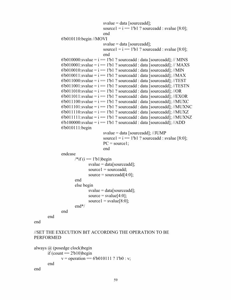
svalue = data [sourceadd]; source1 = i == 1'b1 ? sourceadd : svalue [8:0]; end 6'b010110:begin //MOVI svalue = data [sourceadd]; source1 = i == 1'b1 ? sourceadd : svalue [8:0]; end 6'b010000:svalue = i == 1'b1 ? sourceadd : data [sourceadd]; // MINS 6'b010001:svalue = i == 1'b1 ? sourceadd : data [sourceadd]; // MAXS 6'b010010:svalue = i == 1'b1 ? sourceadd : data [sourceadd]; //MIN 6'b010011:svalue = i == 1'b1 ? sourceadd : data [sourceadd]; //MAX 6'b011000:svalue = i == 1'b1 ? sourceadd : data [sourceadd]; //TEST 6'b011001:svalue = i == 1'b1 ? sourceadd : data [sourceadd]; //TESTN 6'b011010:svalue = i == 1'b1 ? sourceadd : data [sourceadd]; //OR 6'b011011:svalue = i == 1'b1 ? sourceadd : data [sourceadd]; //EXOR 6'b011100:svalue = i == 1'b1 ? sourceadd : data [sourceadd]; //MUXC 6'b011101:svalue = i == 1'b1 ? sourceadd : data [sourceadd]; //MUXNC 6'b011110:svalue = i == 1'b1 ? sourceadd : data [sourceadd]; //MUXZ 6'b011111:svalue = i == 1'b1 ? sourceadd : data [sourceadd]; //MUXNZ 6'b100000:svalue = i == 1'b1 ? sourceadd : data [sourceadd]; //ADD 6'b010111:begin svalue = data [sourceadd]; //JUMP source1 = i == 1'b1 ? sourceadd : svalue [8:0]; PC = source1; end endcase /*if (i == 1'b1)begin svalue = data[sourceadd]; source1 = sourceadd; source = sourceadd[4:0]; end else begin svalue = data[sourceadd]; source = svalue[4:0]; source1 = svalue[8:0]; end*/ end end end //SET THE EXECUTION BIT ACCORDING THE OPERATION TO BE PERFORMED always @ (posedge clock)begin if (count == 2'b10)begin v = operation == 6'b010111 ? 1'b0 : v; end end
59
always @ (posedge clock)begin if (count==2'b10)begin case (operation) 6'b001000:exror=1'b1; 6'b001001:exrol=1'b1; 6'b001010:exshr=1'b1; 6'b001011:exshl=1'b1; 6'b001110:exsar=1'b1; 6'b001111:exrev=1'b1; 6'b010100:exmovs=1'b1; 6'b010101:exmovd=1'b1; 6'b010110:exmovi=1'b1; 6'b010000:exmins=1'b1; 6'b001100:exrcr=1'b1; 6'b001101:exrcl=1'b1; 6'b010001:exmaxs=1'b1; 6'b010010:exmin=1'b1; 6'b100011:exmax=1'b1; 6'b011000:extest=1'b1; 6'b011001:extestn=1'b1; 6'b011010:exOR=1'b1; 6'b011011:exEXOR=1'b1; 6'b011100:exmuxc=1'b1; 6'b011101:exmuxnc=1'b1; 6'b011110:exmuxz=1'b1; 6'b011111:exmuxnz=1'b1; 6'b100000:exadd=1'b1; 6'b010111:exjmp=1'b1; endcase end else if (count == 2'b00)begin case (op) 6'b001000:exror=1'b0; 6'b001001:exrol=1'b0; 6'b001010:exshr=1'b0; 6'b001011:exshl=1'b0; 6'b001110:exsar=1'b0; 6'b001111:exrev=1'b0; 6'b010100:exmovs=1'b0; 6'b010101:exmovd=1'b0; 6'b010110:exmovi=1'b0; 6'b010000:exmins=1'b0; 6'b001100:exrcr=1'b0; 6'b001101:exrcl=1'b0; 6'b010001:exmaxs=1'b0; 6'b010010:exmin=1'b0; 6'b100011:exmax=1'b0;
60
6'b011000:extest=1'b0; 6'b011001:extestn=1'b0; 6'b011010:exOR=1'b0; 6'b011011:exEXOR=1'b0; 6'b011100:exmuxc=1'b0; 6'b011101:exmuxnc=1'b0; 6'b011110:exmuxz=1'b0; 6'b011111:exmuxnz=1'b0; 6'b100000:exadd=1'b0; 6'b010111:exjmp=1'b0; endcase end end // PERFORM THE OPERATION ror r0 (clock,exror,Rror,dvalue,source,condition,roraddress,destadd,c,z); rol r2 (clock,exrol,Rrol,dvalue,source,condition,roladdress,destadd,c,z); shr sh1 (clock,exshr,Rshr,dvalue,source,condition,shraddress,destadd,c,z); shl sh2 (clock,exshl,Rshl,dvalue,source,condition,shladdress,destadd,c,z); sar asr (clock,exsar,Rsar,dvalue,source,condition,saraddress,destadd,c,z); rev rv1 (clock,exrev,Rrev,dvalue,source,condition,revaddress,destadd,c,z); movs mv1 (clock,exmovs,Rmovs,dvalue1,source1,condition,movsaddress,destadd,c,z); movd mv2 (clock,exmovd,Rmovd,dvalue2,dvalue3,source1,condition,movdaddress,destadd,c,z); movi mv3 (clock,exmovi,Rmovi,dvalue4,source1,condition,moviaddress,destadd,c,z); rcr rc1 (clock,exrcr,Rrcr,dvalue,source,condition,rcraddress,destadd,c,z,C_flag); rcl rc2 (clock,exrcl,Rrcl,dvalue,source,condition,rcladdress,destadd,c,z,C_flag); mins min1 (clock,exmins,Rmins,dvalue,svalue,condition,minsaddress,destadd,c,z,Zmins,Gmins); maxs max1 (clock,exmaxs,Rmaxs,dvalue,svalue,condition,maxsaddress,destadd,c,z,Zmaxs,Gmaxs); min min2 (clock,exmin,Rmin,dvalue,svalue,condition,minaddress,destadd,c,z,Zmin,Gmin); max max2 (clock,exmax,Rmax,dvalue,svalue,condition,maxaddress,destadd,c,z,Zmax,Gmax); test t1 (clock,extest,Rtest,dvalue,svalue,condition,testaddress,destadd,c,z,Ztest,Ptest); testn t2 (clock,extestn,Rtestn,dvalue,svalue,condition,testnaddress,destadd,c,z,Ztestn,Ptestn); OR or1 (clock,exOR,Ror,dvalue,svalue,condition,ORaddress,destadd,c,z,ZOR,POR); EXOR exor1 (clock,exEXOR,Rexor,dvalue,svalue,condition,EXORaddress,destadd,c,z,ZEXOR,PEXOR); muxc mux1(clock,exmuxc,Rmuxc,dvalue,svalue,condition,muxcaddress,destadd,c,z,C_flag,Zmuxc,Pmuxc);
61
muxnc mux2 (clock,exmuxnc,Rmuxnc,dvalue,svalue,condition,muxncaddress,destadd,c,z,C_flag,Zmuxnc,Pmuxnc); muxz mux3 (clock,exmuxz,Rmuxz,dvalue,svalue,condition,muxzaddress,destadd,c,z,Z_flag,Zmuxz,Pmuxz); muxnz mux4 (clock,exmuxnz,Rmuxnz,dvalue,svalue,condition,muxnzaddress,destadd,c,z,Z_flag,Zmuxnz,Pmuxnz); add add1 (clock,exadd,Radd,dvalue,svalue,condition,addaddress,destadd,c,z,Zadd,Cadd); jmp jmp1(clock,exjmp,Rsource,Rdest,source1,dvalue1,condition,jmpaddress,destadd,c,z,Zjmp); // WRITE BACK THE RESULT IN MEMORY // SET THE WRITE BACK CONTROL BIT AS PER THE OPERATION always @ (posedge clock)begin if (count == 2'b11)begin case (operation) 6'b001000:wbror=1'b1; 6'b001001:wbrol=1'b1; 6'b001010:wbshr=1'b1; 6'b001011:wbshl=1'b1; 6'b001110:wbsar=1'b1; 6'b001111:wbrev=1'b1; 6'b010100:wbmovs=1'b1; 6'b010101:wbmovd=1'b1; 6'b010110:wbmovi=1'b1; 6'b010000:wbmins=1'b1; 6'b001100:wbrcr=1'b1; 6'b001101:wbrcl=1'b1; 6'b010001:wbmaxs=1'b1; 6'b010010:wbmin=1'b1; 6'b010011:wbmax=1'b1; 6'b011000:wbtest=1'b1; 6'b011001:wbtestn=1'b1; 6'b011010:wbOR=1'b1; 6'b011011:wbEXOR=1'b1; 6'b011100:wbmuxc=1'b1; 6'b011101:wbmuxnc=1'b1; 6'b011110:wbmuxz=1'b1; 6'b011111:wbmuxnz=1'b1; 6'b100000:wbadd=1'b1; 6'b010111:wbjmp=1'b1; endcase end else if (count == 2'b01)begin
62

case (op) 6'b001000:wbror=1'b0; 6'b001001:wbrol=1'b0; 6'b001010:wbshr=1'b0; 6'b001011:wbshl=1'b0; 6'b001110:wbsar=1'b0; 6'b001111:wbrev=1'b0; 6'b010100:wbmovs=1'b0; 6'b010101:wbmovd=1'b0; 6'b010110:wbmovi=1'b0; 6'b010000:wbmins=1'b0; 6'b001100:wbrcr=1'b0; 6'b001101:wbrcl=1'b0; 6'b010001:wbmaxs=1'b0; 6'b010010:wbmin=1'b0; 6'b010011:wbmax=1'b0; 6'b011000:wbtest=1'b0; 6'b011001:wbtestn=1'b0; 6'b011010:wbOR=1'b0; 6'b011011:wbEXOR=1'b0; 6'b011100:wbmuxc=1'b0; 6'b011101:wbmuxnc=1'b0; 6'b011110:wbmuxz=1'b0; 6'b011111:wbmuxnz=1'b0; 6'b100000:wbadd=1'b0; 6'b010111:wbjmp=1'b0; endcase end end // FLIP FLOP THE OPCODE AND RESULT BIT TO USE INTO THE WRITE BACK STAGE always @ (posedge clock)begin if (count==2'b11)begin op=operation; result=r; z1=z; c1=c; end end // WRITE THE RESULT IN MEMORY always @ (posedge clock)begin if (count==2'b00)begin if (wbror==1'b1)begin
63
if (op==6'b001000)begin if (result==1'b1)begin I_out = Rror; R3 = Rror; data [roraddress] = Rror; end end end else if (wbrol==1'b1)begin if (op==6'b001001)begin if (result==1'b1)begin I_out = Rrol; R3 = Rrol; data [roladdress] = Rrol; end end end else if (wbshr==1'b1)begin if (op==6'b001010)begin if (result==1'b1)begin I_out = Rshr; R3 = Rshr; data [shraddress] = R3; end end end else if (wbshl==1'b1)begin if (op==6'b001011)begin if (result==1'b1)begin I_out = Rshl; R3 = Rshl; data [shladdress] = Rshl; end end end else if (wbsar==1'b1)begin if (op==6'b001110)begin if (result==1'b1)begin I_out = Rsar; R3 = Rsar; data [saraddress] = R3; end end end else if (wbrev==1'b1)begin if (op==6'b001111)begin if (result==1'b1)begin I_out = Rrev;
64

R3 = Rrev; data [revaddress] = R3; end end end else if (wbmovs==1'b1)begin if (op==6'b010100)begin if (result==1'b1)begin data [movsaddress] = Rmovs; I_out = Rmovs; R3 = Rmovs; end end end else if (wbmovd==1'b1)begin if (op==6'b010101)begin if (result==1'b1)begin data [movdaddress] = Rmovd; I_out = Rmovd; R3 = Rmovd; end end end else if (wbmovi==1'b1)begin if (op==6'b010110)begin if (result==1'b1)begin data [moviaddress] = Rmovi; I_out = Rmovi; R3 = Rmovi; end end end else if (wbrcr==1'b1)begin if (op==6'b001100)begin if (result==1'b1)begin data [rcraddress] = Rrcr; I_out = Rrcr; R3 = Rrcr; end end end else if (wbrcl==1'b1)begin if (op==6'b001101)begin if (result==1'b1)begin data [rcladdress] = Rrcl; I_out = Rrcl; R3 = Rrcl; end
65

end end else if (wbmins==1'b1)begin if (op==6'b010000)begin if (result==1'b1)begin data [minsaddress] = Rmins; I_out = Rmins; R3 = Rmins; end end end else if (wbmaxs==1'b1)begin if (op==6'b010001)begin if (result==1'b1)begin data [maxsaddress] = Rmaxs; I_out = Rmaxs; R3 = Rmaxs; end end end else if (wbmin==1'b1)begin if (op==6'b010010)begin if (result==1'b1)begin data [minaddress] = Rmin; I_out = Rmin; R3 = Rmin; end end end else if (wbmax==1'b1)begin if (op==6'b010011)begin if (result==1'b1)begin data [maxaddress] = Rmax; I_out = Rmax; R3 = Rmax; end end end else if (wbtest==1'b1)begin if (op==6'b011000)begin if (result == 1'b1)begin data [testaddress] = Rtest; I_out = Rtest; R3 = Rtest; end else begin I_out = Rtest; R3 = Rtest;
66

end end end else if (wbtestn==1'b1)begin if (op==6'b011001)begin if (result == 1'b1)begin data[testnaddress] = Rtestn; I_out = Rtestn; R3 = Rtestn; end else begin I_out = Rtestn; R3 = Rtestn; end end end else if (wbOR==1'b1)begin if (op==6'b011010)begin if (result == 1'b1)begin data[ORaddress] = Ror; I_out = Ror; R3 = Ror; end end end else if (wbEXOR==1'b1)begin if (op==6'b011011)begin if (result == 1'b1)begin data[EXORaddress] = Rexor; I_out = Rexor; R3 = Rexor; end end end else if (wbmuxc==1'b1)begin if (op==6'b011100)begin if (result == 1'b1)begin data[muxcaddress] = Rmuxc; I_out = Rmuxc; R3 = Rmuxc; end end end else if (wbmuxnc==1'b1)begin if (op==6'b011101)begin if (result == 1'b1)begin data[muxncaddress] = Rmuxnc; I_out = Rmuxnc;
67
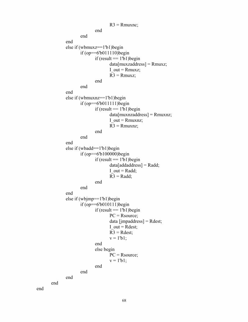
R3 = Rmuxnc; end end end else if (wbmuxz==1'b1)begin if (op==6'b011110)begin if (result == 1'b1)begin data[muxzaddress] = Rmuxz; I_out = Rmuxz; R3 = Rmuxz; end end end else if (wbmuxnz==1'b1)begin if (op==6'b011111)begin if (result == 1'b1)begin data[muxnzaddress] = Rmuxnz; I_out = Rmuxnz; R3 = Rmuxnz; end end end else if (wbadd==1'b1)begin if (op==6'b100000)begin if (result == 1'b1)begin data[addaddress] = Radd; I_out = Radd; R3 = Radd; end end end else if (wbjmp==1'b1)begin if (op==6'b010111)begin if (result == 1'b1)begin PC = Rsource; data [jmpaddress] = Rdest; I_out = Rdest; R3 = Rdest; v = 1'b1; end else begin PC = Rsource; v = 1'b1; end end end end end
68
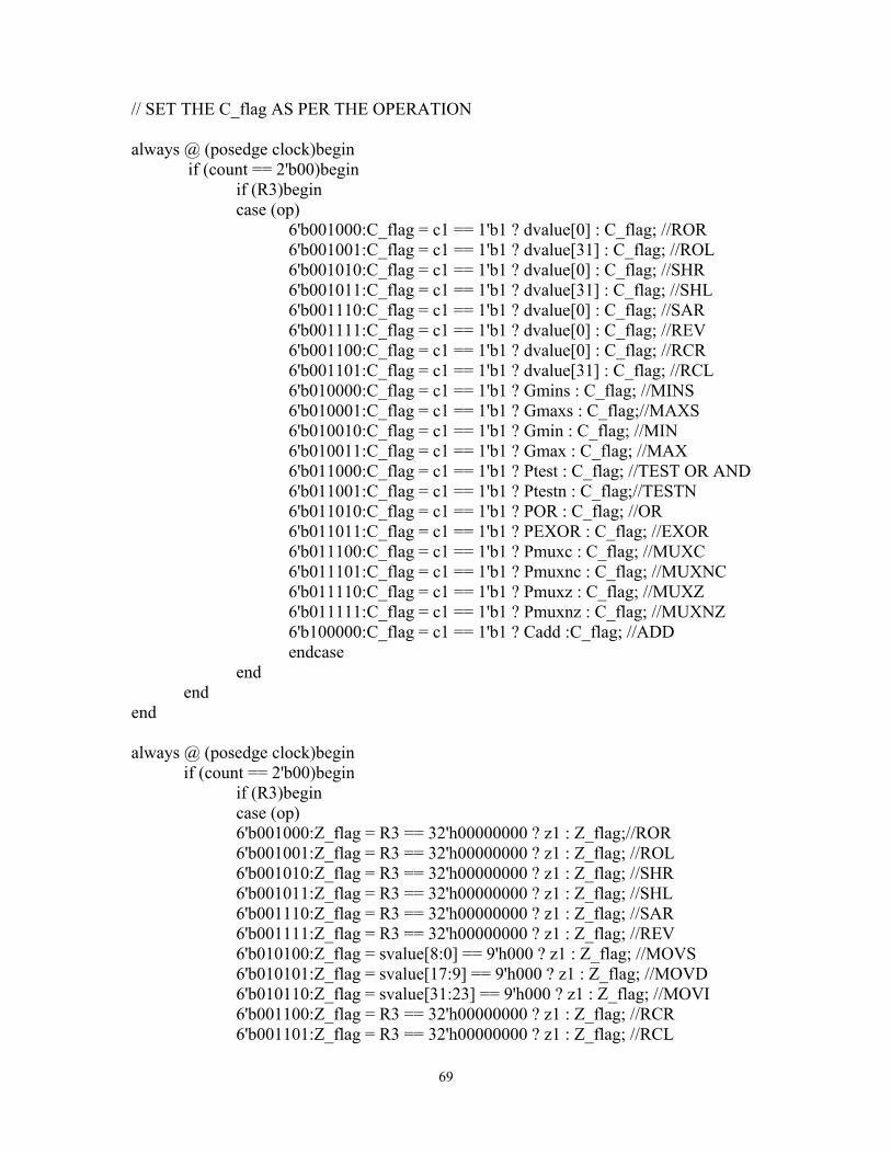
// SET THE C_flag AS PER THE OPERATION always @ (posedge clock)begin if (count == 2'b00)begin if (R3)begin case (op) 6'b001000:C_flag = c1 == 1'b1 ? dvalue[0] : C_flag; //ROR 6'b001001:C_flag = c1 == 1'b1 ? dvalue[31] : C_flag; //ROL 6'b001010:C_flag = c1 == 1'b1 ? dvalue[0] : C_flag; //SHR 6'b001011:C_flag = c1 == 1'b1 ? dvalue[31] : C_flag; //SHL 6'b001110:C_flag = c1 == 1'b1 ? dvalue[0] : C_flag; //SAR 6'b001111:C_flag = c1 == 1'b1 ? dvalue[0] : C_flag; //REV 6'b001100:C_flag = c1 == 1'b1 ? dvalue[0] : C_flag; //RCR 6'b001101:C_flag = c1 == 1'b1 ? dvalue[31] : C_flag; //RCL 6'b010000:C_flag = c1 == 1'b1 ? Gmins : C_flag; //MINS 6'b010001:C_flag = c1 == 1'b1 ? Gmaxs : C_flag;//MAXS 6'b010010:C_flag = c1 == 1'b1 ? Gmin : C_flag; //MIN 6'b010011:C_flag = c1 == 1'b1 ? Gmax : C_flag; //MAX 6'b011000:C_flag = c1 == 1'b1 ? Ptest : C_flag; //TEST OR AND 6'b011001:C_flag = c1 == 1'b1 ? Ptestn : C_flag;//TESTN 6'b011010:C_flag = c1 == 1'b1 ? POR : C_flag; //OR 6'b011011:C_flag = c1 == 1'b1 ? PEXOR : C_flag; //EXOR 6'b011100:C_flag = c1 == 1'b1 ? Pmuxc : C_flag; //MUXC 6'b011101:C_flag = c1 == 1'b1 ? Pmuxnc : C_flag; //MUXNC 6'b011110:C_flag = c1 == 1'b1 ? Pmuxz : C_flag; //MUXZ 6'b011111:C_flag = c1 == 1'b1 ? Pmuxnz : C_flag; //MUXNZ 6'b100000:C_flag = c1 == 1'b1 ? Cadd :C_flag; //ADD endcase end end end always @ (posedge clock)begin if (count == 2'b00)begin if (R3)begin case (op) 6'b001000:Z_flag = R3 == 32'h00000000 ? z1 : Z_flag;//ROR 6'b001001:Z_flag = R3 == 32'h00000000 ? z1 : Z_flag; //ROL 6'b001010:Z_flag = R3 == 32'h00000000 ? z1 : Z_flag; //SHR 6'b001011:Z_flag = R3 == 32'h00000000 ? z1 : Z_flag; //SHL 6'b001110:Z_flag = R3 == 32'h00000000 ? z1 : Z_flag; //SAR 6'b001111:Z_flag = R3 == 32'h00000000 ? z1 : Z_flag; //REV 6'b010100:Z_flag = svalue[8:0] == 9'h000 ? z1 : Z_flag; //MOVS 6'b010101:Z_flag = svalue[17:9] == 9'h000 ? z1 : Z_flag; //MOVD 6'b010110:Z_flag = svalue[31:23] == 9'h000 ? z1 : Z_flag; //MOVI 6'b001100:Z_flag = R3 == 32'h00000000 ? z1 : Z_flag; //RCR 6'b001101:Z_flag = R3 == 32'h00000000 ? z1 : Z_flag; //RCL
69

6'b010000:Z_flag = R3 == 32'h00000000 ? Zmins : Z_flag; //MINS 6'b010001:Z_flag = R3 == 32'h00000000 ? Zmaxs : Z_flag; //MAXS 6'b010010:Z_flag = R3 == 32'h00000000 ? Zmin : Z_flag; //MIN 6'b010011:Z_flag = R3 == 32'h00000000 ? Zmax : Z_flag;//MAX 6'b011000:Z_flag = R3 == 32'h00000000 ? Ztest : Z_flag; //TEST OR 6'b011001:Z_flag = R3 == 32'h00000000 ? Ztestn : Z_flag; //TESTN OR 6'b011010:Z_flag = R3 == 32'h00000000 ? ZOR : Z_flag; //OR 6'b011011:Z_flag = R3 == 32'h00000000 ? ZEXOR : Z_flag; //EXOR 6'b011100:Z_flag = R3 == 32'h00000000 ? Zmuxc : Z_flag; //MUXC 6'b011101:Z_flag = R3 == 32'h00000000 ? Zmuxnc : Z_flag; //MUXNC 6'b011110:Z_flag = R3 == 32'h00000000 ? Zmuxz : Z_flag; //MUXZ 6'b011111:Z_flag = R3 == 32'h00000000 ? Zmuxnz : Z_flag; //MUXNZ 6'b100000:Z_flag = R3 == 32'h00000000 ? Zadd : Z_flag; //ADD 6'b010111:Z_flag = R3 == 32'h00000000 ? Zjmp : Z_flag; //JUMP endcase end end end endmodule
70
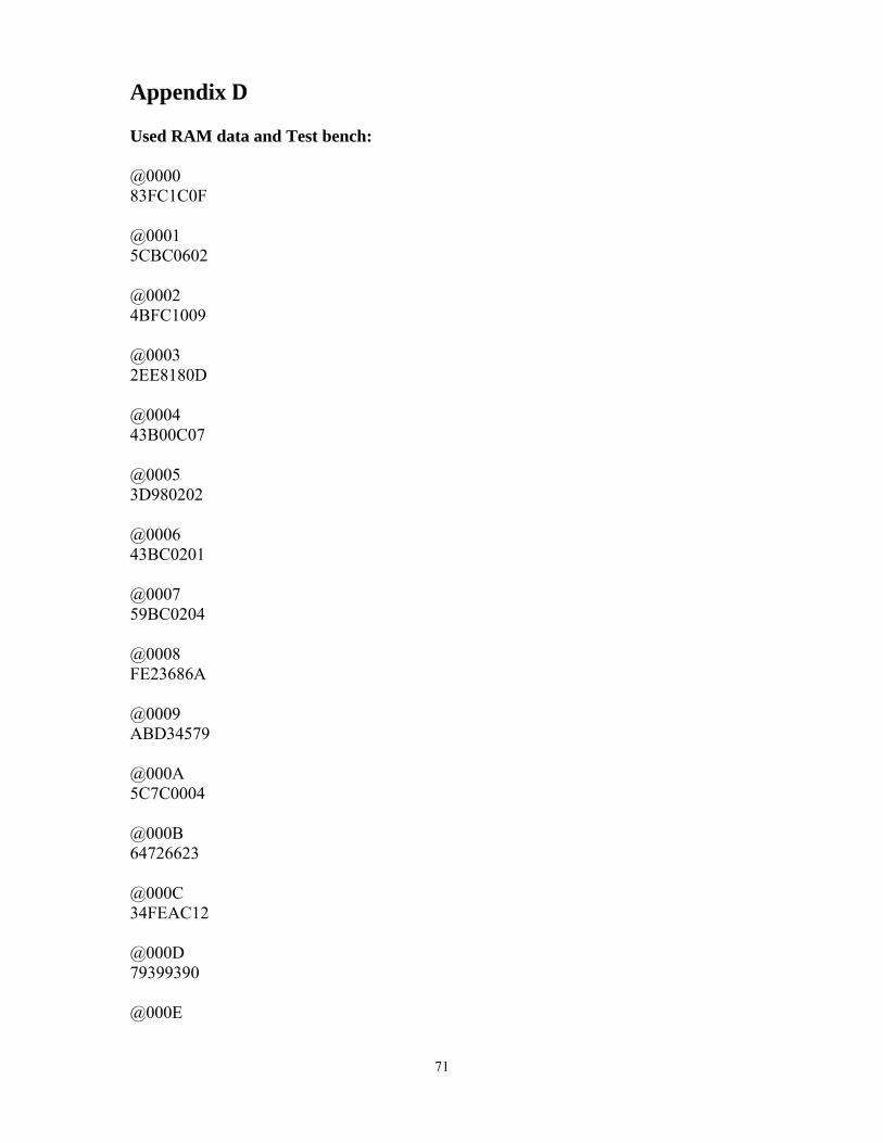
Appendix D Used RAM data and Test bench:
@0000 83FC1C0F @0001 5CBC0602 @0002 4BFC1009 @0003 2EE8180D @0004 43B00C07 @0005 3D980202 @0006 43BC0201 @0007 59BC0204 @0008 FE23686A @0009 ABD34579 @000A 5C7C0004 @000B 64726623 @000C 34FEAC12 @000D 79399390 @000E
71

53500AB4 @000F 8768623A Test bench: `timescale 1ns / 1ps ////////////////////////////////////////////////////////////////////////////////// // Company: // Engineer: // // Create Date: 01:56:23 11/17/2009 // Design Name: // Module Name: t_cog // Project Name: // Target Devices: // Tool versions: // Description: // // Dependencies: // // Revision: // Revision 0.01 - File Created // Additional Comments: // ////////////////////////////////////////////////////////////////////////////////// module t_cog(); reg clock,reset; wire [31:0] I_out; initial begin // $dumpfile("cog.dump"); // $dumpvars(0,t_cog); clock=0; #1000 $finish; end always #12.5 clock = ~clock; cog c1 (I_out,clock,reset); endmodule
72

Appendix E
73
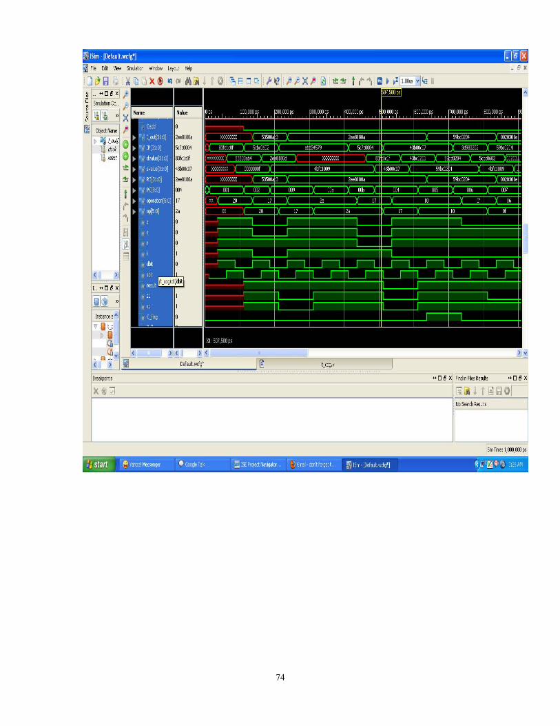
74

75

76
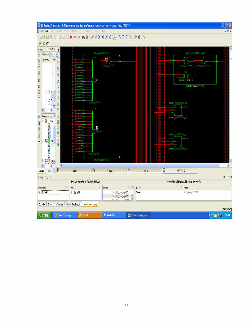
77