1 basic i/o interface a course in microprocessor electrical engineering dept. university of...
TRANSCRIPT

1
Basic I/O Interface
A Course in Microprocessor
Electrical Engineering Dept.
University of Indonesia

2
Isolated and Memory-Mapped I/O
Isolated I/O
The addresses for isolated I/O devices are separate from the memory.
Memory-Mapped I/O
A memory-mapped I/O device is treated as a memory location in the memory map.
(Figure of Isolated I/O and Memory-Mapped I/O)
3
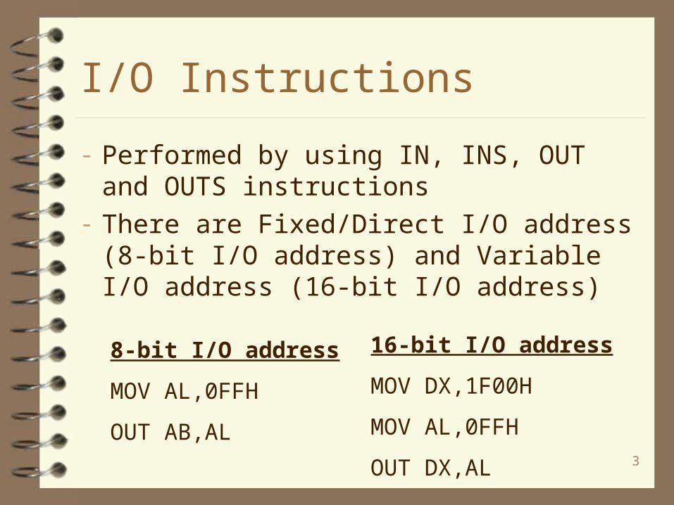
I/O Instructions
- Performed by using IN, INS, OUT and OUTS instructions
- There are Fixed/Direct I/O address (8-bit I/O address) and Variable I/O address (16-bit I/O address) 8-bit I/O address
MOV AL,0FFH
OUT AB,AL
16-bit I/O address
MOV DX,1F00H
MOV AL,0FFH
OUT DX,AL

4
I/O Port Address Decoding
– I/O port address decoding = memory address decoding
– The main difference between memory decoding and isolated I/O decoding is the number of address pins connected to the decoder.
– Another difference is that we use the IORC and IOWC to activite I/O devices for a read or a write operation.
– On earlier versions of the microprocessor, IO/M =1 and RD or WR are used to activate I/O devices

5
I/O Port Address Decoding(cont’d)
– On the newest versions of the microprocessor, the M/IO = 0 and W/R are used to activate I/O devices.
Decoding 8-Bit I/O Address– The fixed I/O instruction uses an 8-bit I/O
port address that appears on A15-A0 as 0000H - 00FFH.
– Fig. 10-6 illustrates a 74ALS138 decoder that decodes 8-bit I/O ports F0H-F7H.
6
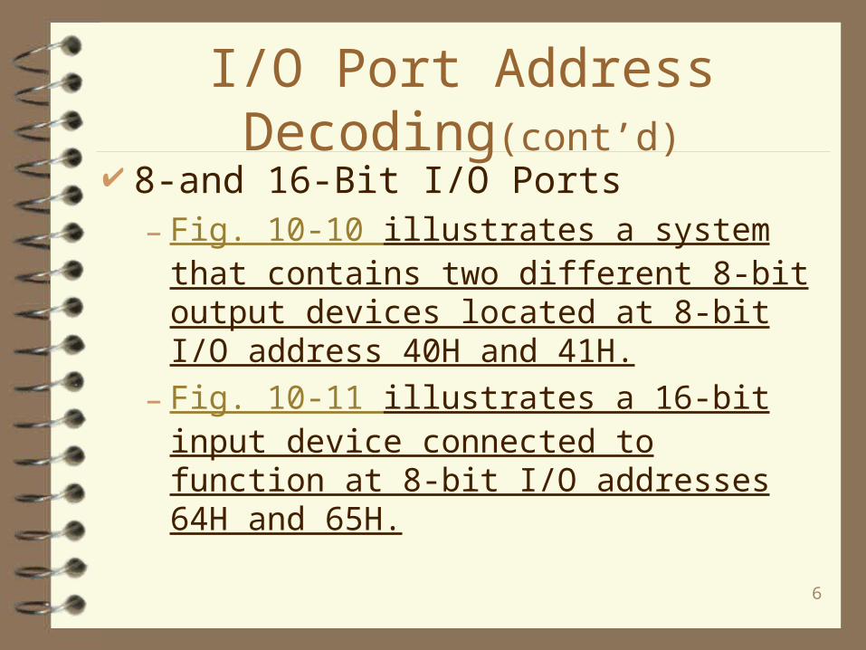
I/O Port Address Decoding(cont’d)
8-and 16-Bit I/O Ports – Fig. 10-10 illustrates a system that contains two
different 8-bit output devices located at 8-bit I/O address 40H and 41H.
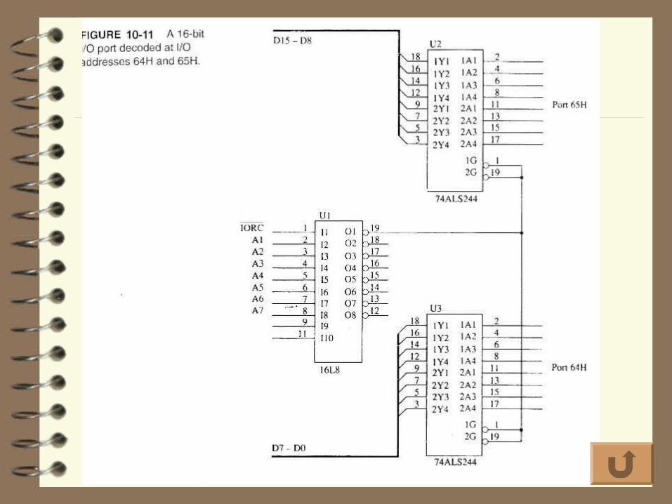
– Fig. 10-11 illustrates a 16-bit input device connected to function at 8-bit I/O addresses 64H and 65H.
7
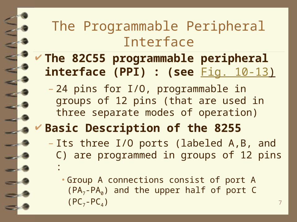
The Programmable Peripheral Interface
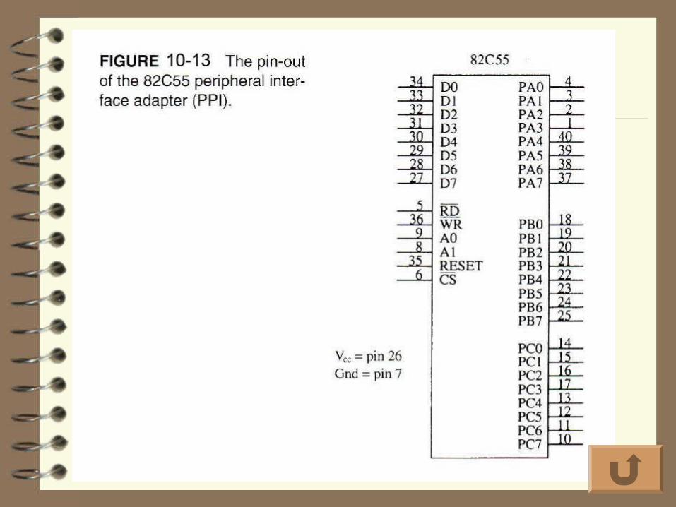
The 82C55 programmable peripheral interface (PPI) : (see Fig. 10-13)– 24 pins for I/O, programmable in groups of 12
pins (that are used in three separate modes of operation)
Basic Description of the 8255– Its three I/O ports (labeled A,B, and C) are
programmed in groups of 12 pins :• Group A connections consist of port A (PA7-PA0)
and the upper half of port C (PC7-PC4)

8
The Programmable Peripheral Interface (cont’d)
• Group B consists of port B (PB7-PB0) and the lower half of port C(PC3-PC0)
– The 82C55 is selected by its CS pin for programming, for reading or writing to a port.
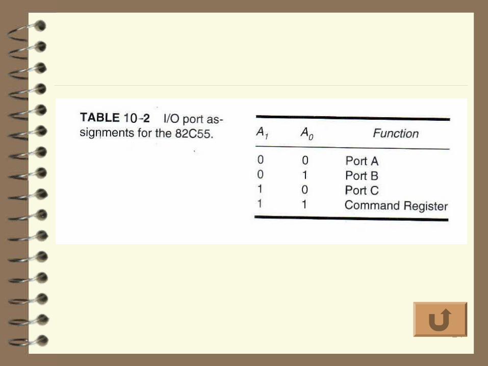
– Register selection is accomplished through the A1 and A0 input pins, which select an internal register for programming or operation

9
The Programmable Peripheral Interface (cont’d)
– Table 10-2 shows the I/O port assignments used for programming and access to the I/O ports.
– Fig. 10-14 shows an 82C55 connected to the 80386SX so that it functions at 8-bit I/O port address C0H (port A), C2H (port B), C4H (port C) and C6H(command register)
– uses the low bank of the 80386SX IO map – RESET input to the 82C55 initializes the device
whenever the microprocessor is reset.

10
The Programmable Peripheral Interface (cont’d)
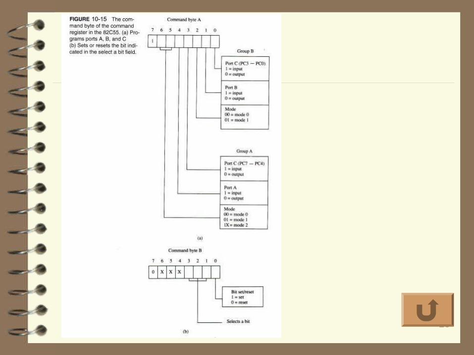
Programming the 82C55
– is easy to program (see Fig. 10-15) notice that bit position 7 selects either command byte A or command byte B :• Command byte A programs the function of
group A & B• Command byte B sets (1) or reset (0) bits of
port C only if the 82C55 is programmed in mode 1 or 2

11
The Programmable Peripheral Interface (cont’d)
– Group B pins (port B and the lower part of port C) are programmed as either input or output pins. Group B can operate in either mode 0 or mode 1
– Group A pins (port A and the upper part of port C) are also programmed as either input or output pins. The difference is that group A can operate in modes 0, 1, and 2

12
The Programmable Peripheral Interface (cont’d)
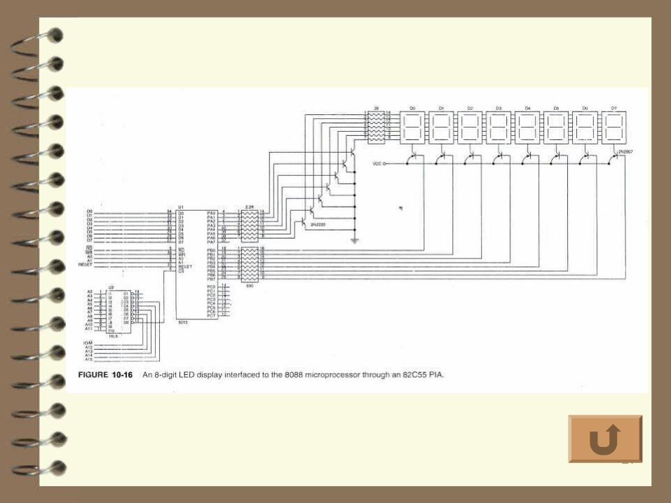
Mode 0 operation– causes the 82C55 to function as either a
buffered input device or as a latched output device
– Fig. 10-16 shows the 82C55 connected to a set of eight 7-segment LED displays (see also Example 10-9)

13
The Programmable Peripheral Interface (cont’d)
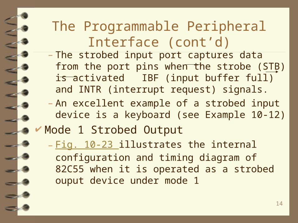
Mode 1 Strobed Input– causes port A and /or port B to function as
latching input devices • this allows external data to be stored into the port
until the microprocessor is ready to retrieve it
– Port C is also used in mode 1 operation for control or handshaking signals that help operate either or both port A and port B as strobed input ports (see Fig. 10-21)
14
The Programmable Peripheral Interface (cont’d)
– The strobed input port captures data from the port pins when the strobe (STB) is activated IBF (input buffer full) and INTR (interrupt request) signals.
– An excellent example of a strobed input device is a keyboard (see Example 10-12)
Mode 1 Strobed Output– Fig. 10-23 illustrates the internal configuration
and timing diagram of 82C55 when it is operated as a strobed ouput device under mode 1
15
The Programmable Peripheral Interface (cont’d)
– Whenever data are written to a port programmed as a strobed output port, the OBF (output buffer full) signal becomes a logic 0 to indicate that data are present in the port latch (study Fig. 10-24 and Example 10-13)
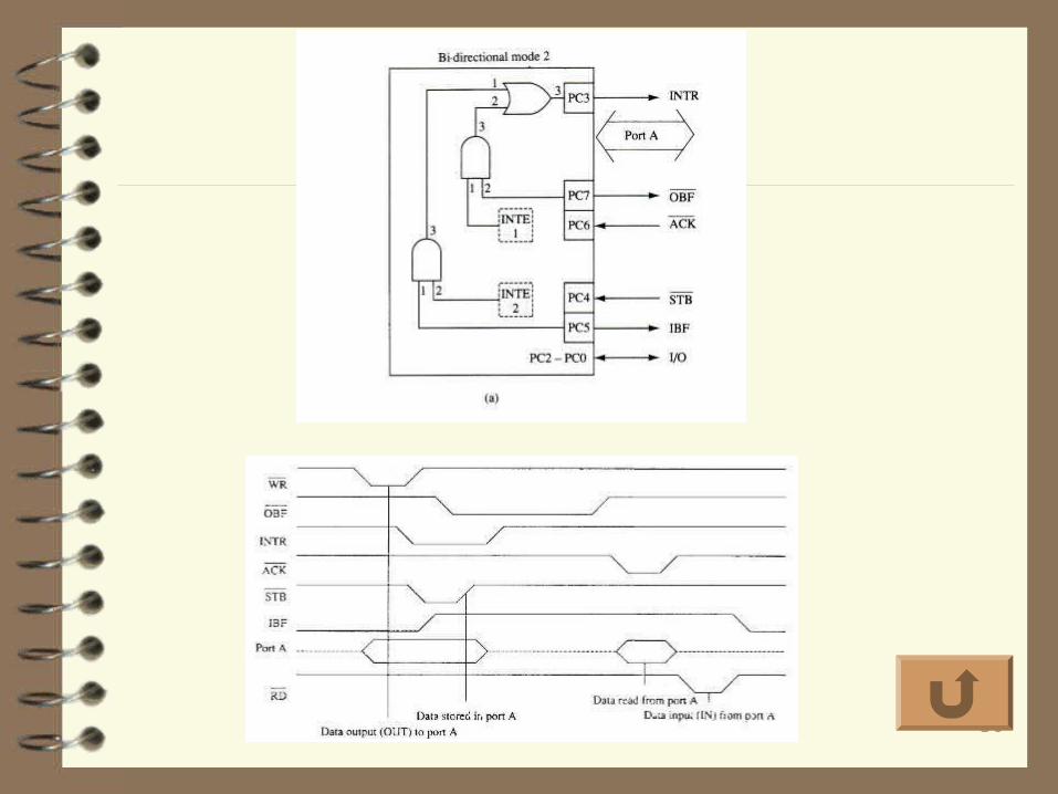
Mode 2 Bidirectional Operation– in mode 2, only group A is allowed (see
Fig. 10-25)– The Bi-directional Bus is used by referencing
port A with the IN and OUT instructions
16
The Programmable Peripheral Interface (cont’d)
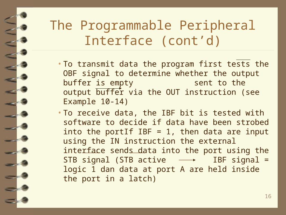
• To transmit data the program first tests the OBF signal to determine whether the output buffer is empty sent to the output buffer via the OUT instruction (see Example 10-14)
• To receive data, the IBF bit is tested with software to decide if data have been strobed into the portIf IBF = 1, then data are input using the IN instruction the external interface sends data into the port using the STB signal (STB active IBF signal = logic 1 dan data at port A are held inside the port in a latch)

17
The Programmable Peripheral Interface (cont’d)
• IBF bit is cleared and the data in the port are moved into AL, when the IN instruction executes (study Example 10-15)
• The INTR (interrupt request) pin can be activated from both directions of data flow through the bus
Fig. 10-26 shows a graphical summary of the three modes of operation for the 82C55

18
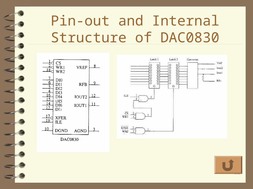
ADC and DAC Converters
Are used to interface the microprocessor to the analog world
The DAC0830 (see Fig. 10-48 & 10-49)– is connected to the microprocessor as illustrated
in Fig. 10-50
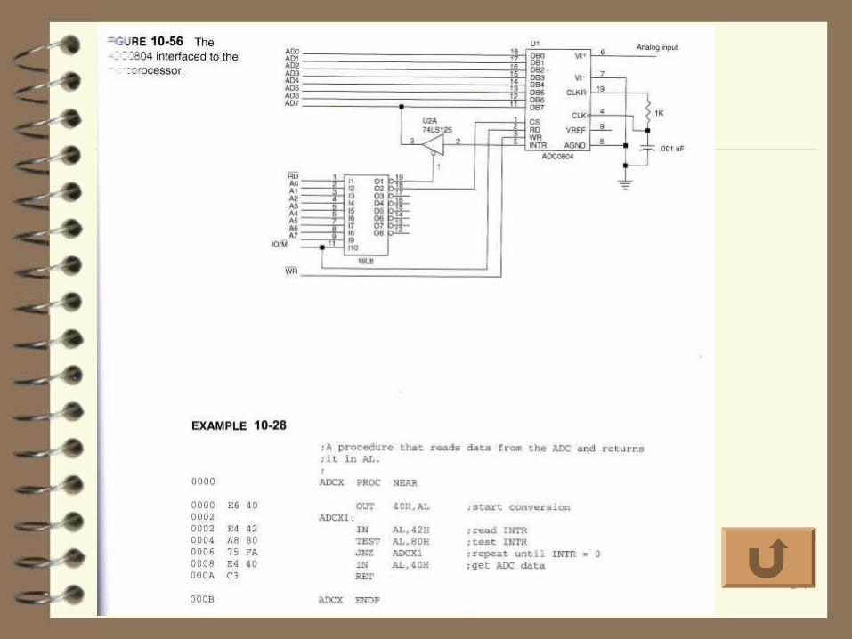
Study The ADC0804 Study Fig. 10-56 dan Example 10-28

19

20

21
22
23
24

25
26
27

28

29
30

31
32
Pin-out and Internal Structure of DAC0830

33
34