mm111 - dtic.mil · rockwel contrtioa copoato deic interia 7l62zscal9 gdii it. cotrollig offc na m...
TRANSCRIPT

AO-AOS& 230 ROCKWELL INTERNATIONJAL THOUSAND OAKS CA ELECTRONCS--ETC F/6 lf&2HIGH CONTRAST ELECTROt.UMINESCENT NWE(RIC READOUT DEVICE (U)AUG 80 m K KILCOYME DAA807-78-C-24qA
UNCLASSIFIED ERC%10I.15IRF DLET-TO-78-29%-a Nmm111"7.
i 3 * WE:. 30 112.0
11111 I___1 lfl 1.
MICROCOPY RESOLWTION TEST CHART
NATIONAL BURIAL) I STANDJAR), 11, A

Research and Development Technical ReportDELET-TR-78-2996-2
D- HIGH CONTRAST ELECTROLUMINESCENTNUMERIC READOUT DEVICE
o M. K. KilcoyneROCKWELL INTERNATIONALThousand Oaks, CA 91360
August 1980
Second Interim Report for Period I Feb. 79 - 31 May 79
DISTRIBUTION STATEMENT DTICApproved for public release; distribution unlimited. LECT ft
AUG 22 198~
Prepared for: AELECTRONICS TECHNOLOGY & DEVICES LABORATORY
ERADCOMUS ARMY ELECTRONICS RESEARCH AND DEVELOPMENT COMMANDFORT MONMOUTH, NEW JERSEY 07703
80HISA-FM 7180 822 015

NOTICES
Disclaimers
The citation of trade names and names of manufacturers inthis report is not to be construed as official Governmentindorsement or approval of commercial products or servicesreferenced herein.
Disposition
Destroy this report when it is no longer needed. Do notreturn it to the originator.
HISA-FM41378

UNCLASSIFIED-SECURITY CLASSIFICATION OF THIS PAGE (When. 04*a EfntWre
'/REPORT DOCUMENTATION PAGE REOE" COMPLETINOR
H.E.L~iloTn-75DAAO7-8-C299
Rockwel CONTRTioa Copoato DEIC InteriA 7L62ZScal9 GDiI
it. COTROLLIG OFFC NA M NA ESETV
7. ATNORS) . CONTRASSCTIO OGRA O N
9. PERFRINTORNATEN NAMf AND R DRSS1.RGRMELMNTROETTS
Flc or publirch reeae; ditRbuio unlimitedNUMER
chRcerlItationa f orpprimetliodel of75 a ig-cntas nmei 9 elct luine-
1.NTmROI G ispIay uNing AN tAnsRE t elctoun .cn fthinfm wihi
altric cpteroutpu dat pricessinbo ifor ain wit fievl lgc~eDO ~ ~ ~ ~ ~ ~ ~ ~ ~ 3 NUBE O 43 STINOFINO6 S S@IEE wEsi
SECURTY CL sIAT OEASFITHI PAGE tRY. Ata ate
SCEDL

UN1DCLASSIFIEDICCUmYIT CLAS8IPICAIOU OP TWO$ PAGGMM Data AMe.
level and BCD) input.
UNCLASS~flTSCUNTY OLAGPICAtIOW OP ?HgS PASUMb MOSIe 8041E

9 Rockwell International
ERC41016.15IRF
TABLE OF CONTENTS
Page
1 SUMMARY .......... ..................... 1
2 PROGRAM AIMS AND OBJECTIVES ..... ......... .2
3 DECODER - DRIVER CIRCUIT DESIGN AND FABRICATION . 3
3.1 Logic Circuit Design ... ............. 3
3.2 High-Voltage Driver Circuit Design ..... 6
3.2.1 Test Chip Layout .......... 113.2.2 Complimentary High-Voltage Driver
Array .... ................ .... 13
4 HYBRID CIRCUIT LAYOUT AND ASSEMBLY ....... ... 16
5 HIGH-CONTRAST DISPLAY PERFORMANCE ........ ... 19
6 HERMETIC SEAL DESIGN AND FABRICATION ...... . 21
6.1 Requirements ....... ................ 216.2 Design and Fabrication ............. .... 21
V. , "
S 4. .' . -
4 '
11

Rockwell International
ERC41016.15IRF
LIST OF FIGURES
Figure En
I Original Breadboard Circuit Schematic ... . 4
2 Semicustom Logic Chip Schematic .. ....... 5
3 Logic Chip Diagram with Pinouts ... ....... 7
4 High-Voltage Driver Circuit Diagram .. ..... 10
5 High-Voltage Test Chip Layout .... ........ 12
6 Complimentary DMOS Approach .... ......... 14
7 High-Voltage Driver Array ... .......... 15
8 High-Contrast Display Configuration .. ..... 20
9 Hermetic Seal Design ... ............ .. 22
10 Package Component Parts ........... 24
11 Frit Sealed Subassembly .............. .... 25
12 Sealed Package Configuration ........ 26
LIST OF TABLES
Table ale
I Logic Chip Pinouts and Bonding Pad
Designations . . .......... . . .. 8
II High-Voltage Driver Development Schedule . . 17
III Hybrid Circuit Area Requirements . . . . . . 18
4

Rockwell Intemational
ERC41016.15IRF
1. SUMMARY
The Rockwell Electronics Research Center has completed the second
phase of the development program encompassing the design, fabrication,
and characterization of experimental models of a high-contrast numeric
electroluminescent readout device. This device consists of two-digits of
seven-segment numeric displays using a transparent electroluminescent
thin film with high-contrast background layer. The device also contains
with its hermetically sealed package, logic and drive circuitry to operate
the numeric displays from a typical computer output data processing
information, with five volt T2L logic level and BCD input. The package
design also allows the devices to be arranged so that a multi-digit
computer-type terminal readout can be fabricated from a series of individual
packages.
This report covers the work completed during the fourth through the
eighth months of effort. During this period, logic and decoder electronics
have been committed to a semi-custom integrated circuit chip design.
Several designs for high-voltage drivers were evaluated and the final high-
voltage driver approach selected. A process has been developed for hermetic
sealed packages having vertical interconnects for transmitting signals
from the driver electronics vertically to the thin film EL display.
Further electrical and optical tests have been conducted on high-contrast
materials and on sample EL devices to characterize electro-optical para-
mters. Evaluation and analysis of these results are reviewed in detail
in the following sections.

Rockwell Intemational
ERC41016. 1511P
2. PROGRAM AIMS AND OBJECTIVES
The objective of this program is to design and fabricate a quantity of
numeric EL display devices containing two-digits consisting of seven
segments and a decimal point. Four (4) exploratory development models will ibe fabricated each consisting of a ten-digit display made up of five of
the two-digit numeric devices assembled into a suitable socket or printed
circuitboard. Drive circuitry and decoding logic will be included in the
device to allow operation directly from computer level logic inputs at
TTL voltage levels. The display medium shall be a transparent AC thin
film electroluminescent type with a high-contrast background layer for
viewing in high-light ambience. The operational characteristics of the
devices shall be designed to allow uniform electronic dimming of the display
to luminance levels in the order of the 10 ft-L for compatability with
night vision applications. The display shall be capable of sufficient con-
trast to be viewed in an ambient illumination of 10,000 ft-C without additional
contrast enhancement techniques. The devices shall be capable of operation
for a minimum of 3,000 hours at a luminance level that satisfies the
condition of visibility under high-ambient illumination described above.
Also, the devices shall operate without the loss of significant light
emitting areas due to any failure or degradation mechanism during the
3,000 hour/lifetime.
4

91 Rock 'well International
ERC41O16. 15IRF
3. DECODER - DRIVER CIRCUIT DESIGN AND FABRICATION
3.1 Logic Circuit Design
Figure 1 shows the original circuit in which the logic functions
and driver circuitry were evaluated. Figure 2 shows the circuit resulting
from that evaluation from which the design for the semi-custom integrated
logic chip vas taken. To accommodate multi-digit displays one modification
was made from the original circuit. The digit select and enable functions
on pin five and pin six, (Fig. 1), vere modified to a digit strobe circuit
in which either digit can be selected with its own strobe pulse. This
modification was made as a simplification for addressing multiple chips of
two digits each so that all digits are directly accessible by means of a
strobe without the necessity of a digit select function.
The functions on the logic chip consist basically as follows:
A five K~z clock is used to generate the drive frequency for the AC
operation of the TFKL display. The circuit utilizes a latched BCD to
7-segment decoder/driver signal circuit. The 7-segment output signals
are toggled by the display frequency input which causes the selected
segment outputs to be a square wave at the clock input frequency. With
the clock frequency square wave present the selected segments will have a
square wave output that is 180% out of phase with the display frequency
input. Those segments which are not selected will have a square wave output
that is in phase with the input.
The mask layout and bonding pad designations have been received from
the vendor. After some modifications to simplify hybrid circuit layout,I
3

9Rockwell International
ERC4 1016. 15IRF
0
CO10
v.4
4"4
p"4
INI.4.4

9D Rockwell International
ERC4 1016. 15IRP
rrX1*
x I
1z,
'44avsU
CU
'a'..
N n 4. L4

9D Rockwell International
ERC41016.15IRF
the pinouts have been finalized as shown in Fig. 3. A complete listing of
pinouts and bonding pad designations are given in Table I. In the table
pin numbers refer to the pinouts in the 40-pin package in which the first
samples will be received for design verification. The package chips will
also be utilized for evaluation with the high-voltage test chips referred
to in a later section of this report. The packaged logic chips will be
evaluated with the high-voltage test chips driving EL numeric displays to
assure total design compatibility.
The chip bonding pads are designated by letters and refer to the
bonding locations on the die for hybrid circuit layout considerations in the
two-digit package. The chip site (bonding pad) locations have been optimized
for the hybrid circuit layout with respect to high-voltage driver chip
input locations.
The five KHz oscillator circuit is driven from bonding pad locations
RR, SS, and TT.
The chip consists of a logic circuit to decode incoming BCD information
and also contains active components of the five KHz onboard oscillator
circuit. The pa. 4e components of the five KHz oscillator are shown in
Fig. 3 in schematic form they are connected to pads RR, SS, and TT.
3.2 High-Voltage Driver Circuit Design
The original prototype circuit shown in Fig. 1 references a dionics
DI 702 high-voltage driver array chip. However, test driver arrays provided
by the vendor did not meet voltage and current requirements as originally
proposed by the vendor. Further samples also failed to meet requirements
and, therefore, a discrete transistor driver array was used in prototype
evaluation.

9D Rockwell InternationalASSEML DT.ArRA&1 40-PIN DUAL-IN-IE ERC4116.15IRF
dp, Sgz fl a, t I el d, c,'
J H F D C A711 34RC-
:a: RR
a a aa Ua U a a a: aV aj ai
C. 22 a 0 a no, c..: a a a-^I B
a ---- 0 2; 20: 21 21: a a' V..
A T: , d:jua 199:.--a I-rIA: s APa
B-s- S2ZE 136 113
zg 3oi Ci DiagEE wit HPliit
RI 154

9 q Rockwell International
ERC41016. 15IRF
TABLE I
PINOUT (TENTATIVE)
PIN I CHIPSITE CIRCUIT NAME
1 F &I2 H fi3 J . 14 K dp5678 M9 P
10 S 221 T1- U13 W 2014 X dp2151617 y 1218 Z f219 BB a220 CC b221 DD22 EE d223 FT C224 HK252627 KK + Enable 228 LL + Enable 129 mm VDD30 NN BP31 PP 3.32 RR C33 ss R34 IT RC3536 A Ci37 B di38 C tf39 D bi40
8
OD Rockwell International
ERC41016. 15IRF
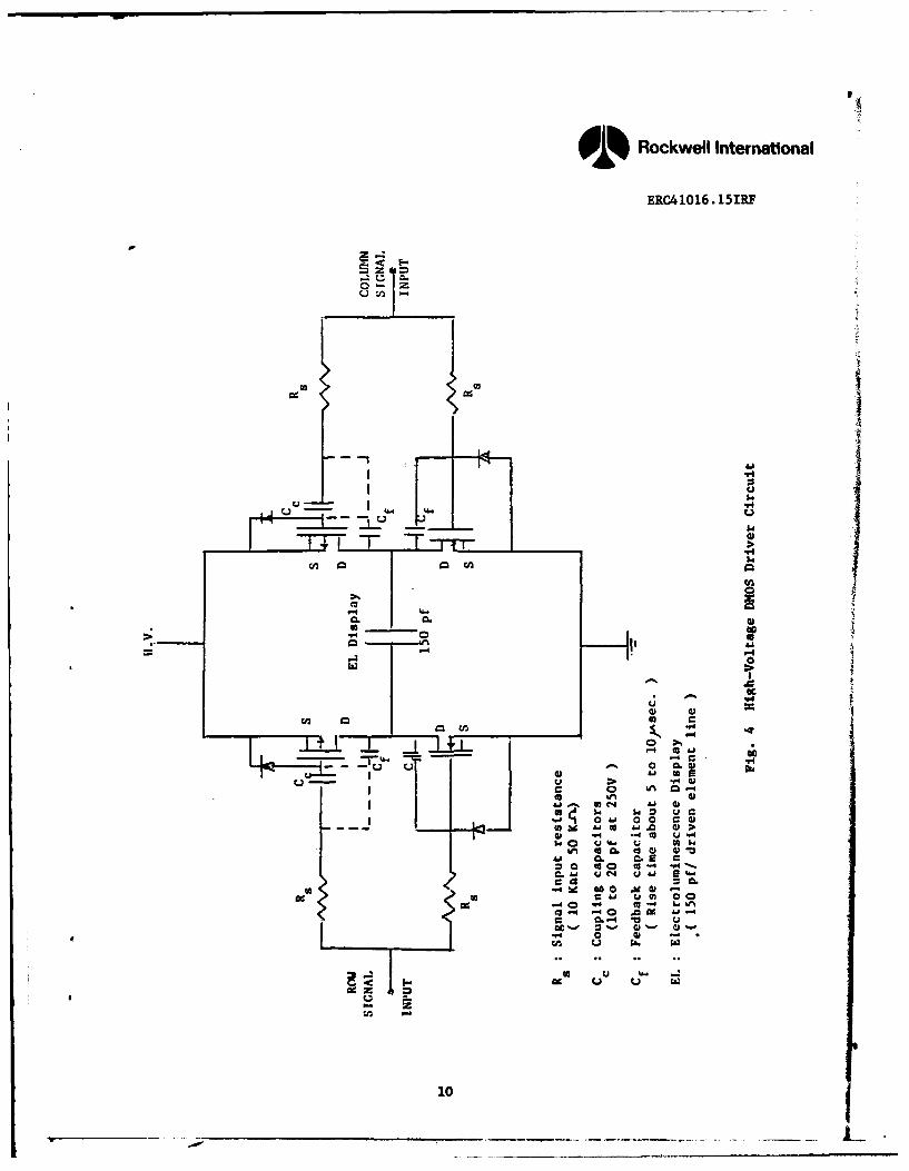
The originally proposed chips would not meet requirements, several
other approaches to the high-voltage drivers were evaluated. While
several approaches would meet electrical requirements, these circuits
were in discrete form and not available in integrated array chips
necessary to meet size and space requirements in the two-digit EL display
package.
Fortunately, Rockwell in a similar program, has under development
a DMOS high-voltage driver array chip. Since this chip is not available
until late December, 1979, a delay in the program would be required to
utilize the DMOS driver chip. The timing was discussed with the contract
monitor and a request for delay of final hardware deliveries has been
proposed to allow utilization of the DMOS driver arrays.
Table II shows a time schedule of development of the devices.
The program is divided into two phases. Phase one involves designing test
masks and fabricating test devices in order to optimize device performance
and device processing. The second phase will involve the integration of the
optimized processing into a single chip containing nine n-channel and nine
p-channel MOSFETS connected in complimentary pair arrays. Each array
(see Fig. 4) will consist of an n- and a p-channel device with the necessary
resistors and coupling capacitors required for signal switching and wave
shaping.
There are several major advantages of the complimentary DMOS process
over the bi-polar approach. First of course, is the direct interface
compatibility to other CMOS logic circuitry. Secondly, the MOSFET devices
have negligilbe leakage currents in the gates and therefore negligible
9
9Rockwell International
ERC4 1016. 15IRP
0-
~-P4
IdI0t
54.
z 0
(AA
- {. 4 ju~10

Rockwell Intemational
ERC41016. 15RPF
charged storage problems. This results in much smaller coupling capacitors
required for voltage isolation from the logic circuitry. Turn off and
turn on delay times of 10 to 20 nano seconds show the high speed response
of the DMOSFET. Another advantage is more packing density per unit area
with the MOS process than is possible with bi-polar devices due to their
dielectric isolation requirements. Also, the more simplified DMOS
process results in significantly lower cost. Based on quotations for
both technologies, the volume cost of the DMOS integrated circuit chips
was about one third of that for the bi-polar approach. In addition, the
bi-polar approach was available only in separate chips one having npn
and the other pnp devices.
The first phase of the DMOS transistor development should be completed
by September, high-voltage transistor arrays will be available by December,
1979.
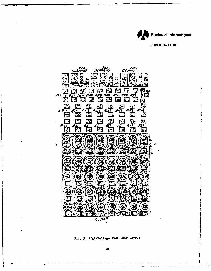
3.2.1 Test Chip Layout
Figure 5 shows the layout of the test chip. The chip will
have in one section 40 test cells to allow for variation of the parameters
to optimize the cell characteristics. Also, as seen on the chip other test
components will be included for the purposes of evaluating chip processing
and doping levels and also for stitch bonding "outboard" capacitors and
resistors and other components such as small MOSFETS and invertors which
may be used for various circuit purposes. The total chip size of the test
chip is 100 x 155 ails. The test chip will be processed in both n-channel
and p-channel versions and chips of this type will be available in September,
1979.
11
9Rockwell International
ERC41Ol6.15IRF
A*, A&-fpa -9
AOF f/I_ APi If/ sl
nsoEs
T, 707I
- 'tiii47
~)791 aMA I
r~
0 ~ T*
Fig. 5 High-Voltage Test chip LayoUt
12I

91% Rockwell International
ERC41016. 15IRF
3.2.2 Complimentary High-Voltage Driver Array
The diagram depicting the complimentary DMOS approach is
shown conceptually in Fig. 6. In this approach the n- wafer would be
used as anticipated for non-epi n-channel processing. The process steps
would be essentially those for non-epi processing. In addtion, a large
p-well would be difused into the surface creating a p- lightly doped area
which would withstand 250 volts from the substrate with acceptable leakage
levels. This approach would allow the processing of an n-channel device
within the p-well on the same chip with both n- and p-channel devices having
250 volts source to drain voltage switching capability.
Figure 7 shows the proposed high-voltage complimentary driver
array. The device has already been size estimated by the vendor at 100 x 120
mils per complimentary chip containing nine p-channel and n-channel drivers
as described above. The vendor has agreed to give the complimentary approach
the highest priority as it substantially simplifies assembly and reduces
assembly cost and complexity. The vendor already has demonstrated 400 volt
switching capability on n-channel and p-channel devices and separate chips
which can be utilized if necessary.
13

'Rockwell International
ERC4 1016. 15IRF
IL0
>U
0;
44
II
14

9D Rockwell InternationalERC41O16. 151RP
HIGH VOLTAGE DRIVER ARRAY
S QI
Figure 7
' Rockwell International
ERC41O16. 15IR1
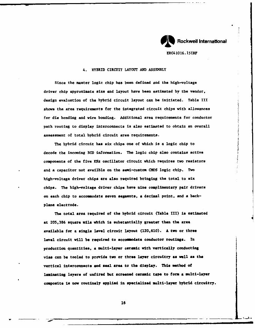
4. HYBRID CIRCUIT LAYOUT AND ASSEMBLY
Since the master logic chip has been defined and the high-voltage
driver chip approximate size and layout have been estimated by the vendor,
design evaluation of the hybrid circuit layout can be initiated. Table III
shows the area requirements for the integrated circuit chips with allowances
for die bonding and wire bonding. Additional area requirements for conductor
path routing to display interconnects is also estimated to obtain an overall
assessment of total hybrid circuit area requirements.
The hybrid circuit has six chips one of which is a logic chip to
decode the incoming BCD information. The logic chip also contains active
components of the five KHz oscillator circuit which requires two resistors
and a capacitor not availble on the semi-custom CMOS logic chip. Two
high-voltage driver chips are also required bringing the total to six
chips. The high-voltage driver chips have nine complimentary pair drivers
on each chip to accommodate seven segments, a decimal point, and a back-
plane electrode.
The total area required of the hybrid circuit (Table III) is estimated
at 205,386 square mils which is substantially greater than the area
available for a single level circuit layout (120,610). A two or three
level circuit will be required to accommodate conductor routings. In
production quantities, a multi-layer ceramic with vertically conducting
vias can be tooled to provide two or three layer circuitry as well as the
vertical interconnects and seal area to the display. This method of
laminating layers of unfired but screened ceramic tape to form a multi-layer
composite is now routinely applied in specialized nulti-layer hybrid circuitry.
16

0 Rockwell Intemational
ERC4 1016. L5IRF
TABLE II
High-Voltage Driver Development Schedule
Feb. 23 ro Ahead
April 26 Ag. 23 DeliverNak Review Test Chip&
WORK WEEK 500 N-Lbannal100 P-Chananel
A. Pase 1 2 384 6 76 9 10 11 12 13 14 15 16 17 18 19 20 21 22 23 24 25 I6
TASK
Tesc seek defiaition ,
Test mask design I
Test mask layout I--4
Hook making
Proc.ss admtorl Specification
N-clummal process 1 Test htum .- 1 . Ca ritimt-IlvslutLoa
P-channel process 2 I -& Optimi ation
Nov. 23Deliver Integrated Driver
Circuit1500 Chips Total
WK lM 750 N-Channel750 P-Chanmel
1. Phasl It 24 25 26 27 26 29 30 31 32 35 36 35 36 37 38 39
TASK
"Hak doe gm,
MSfk layout
Naa.&madklm I I-
N-Uhaoul processin g
Po-danmul proeessing
yvalmation,
1.7

9 Rockwell International
ERC4 1016. 5IRP
TABLE III
LISA IISCLUDU
AMI ARIA INUIN! Dip vinI SONISIIICHIP/FtUNCTION D RIN OW NILS So. NILS UI0NDfl-SQ. NILS ALLOWAmC-SQ. MILS
Logic Chip 136 a 136 18,496 21.316 30.976
CapacitorlOac. 40 z 30 2,000 3,000 3,000
lesiator/O-c. 0 a 1 ,000 3.000 3.000
Re aitor/Oac. Stability 40 z 50 2.000 3.000 3,000
HUih Voltage Driver 100 z 120 12,000 14,300 22,400Diagram I
High Voltage Driver 100 z 120 12,000 14,300 22,400Diagram 2
48,496 58.916 84,776
Area required for conductor routing co diaplay 120,610
Total area required - hybrid circuit 205,386*
Area available - hybrid circuit - I level 120,000
Area available - hybrid circuit - 2 levels 230.400
Area available - hybrid circuit - 3 levels 332.800
• Total hybrid circuit area required amy be reduced somewhet Ia 2 & 3 levelcircuitry where croeovers and viaa may reduce conductor path lengthe.
18

91 Rockwell International
ERC41O16. 15IRF
5. HIGH-CONTRAST DISPLAY PERFORMANCE
A design for high-contrast EL displays utilizing conductive high-
contrast layers has been implemented. The approach utilizes a light
abosrbing insulator film in combination with a transparent conductive
coating that closely matches the refractive index of the 7059 glass
substrate material. Since both the light absorbing film and the trans-
parent conductor closely match the index of the substrate front surface,
reflections are substantially reduced as suggested by measurements report-
ed in Interim Report # 1.
The light absorbing film is utilized in all areas of the display
that are not active. Reflections in the active segment areas are reduced
by controlling the total thickness of the phosphor insulator sandwich so
that it is in an interference mode over the visible spectrum. In
addition, a conductive light absorbing film is applied between the phosphor
and the metal book electrode.
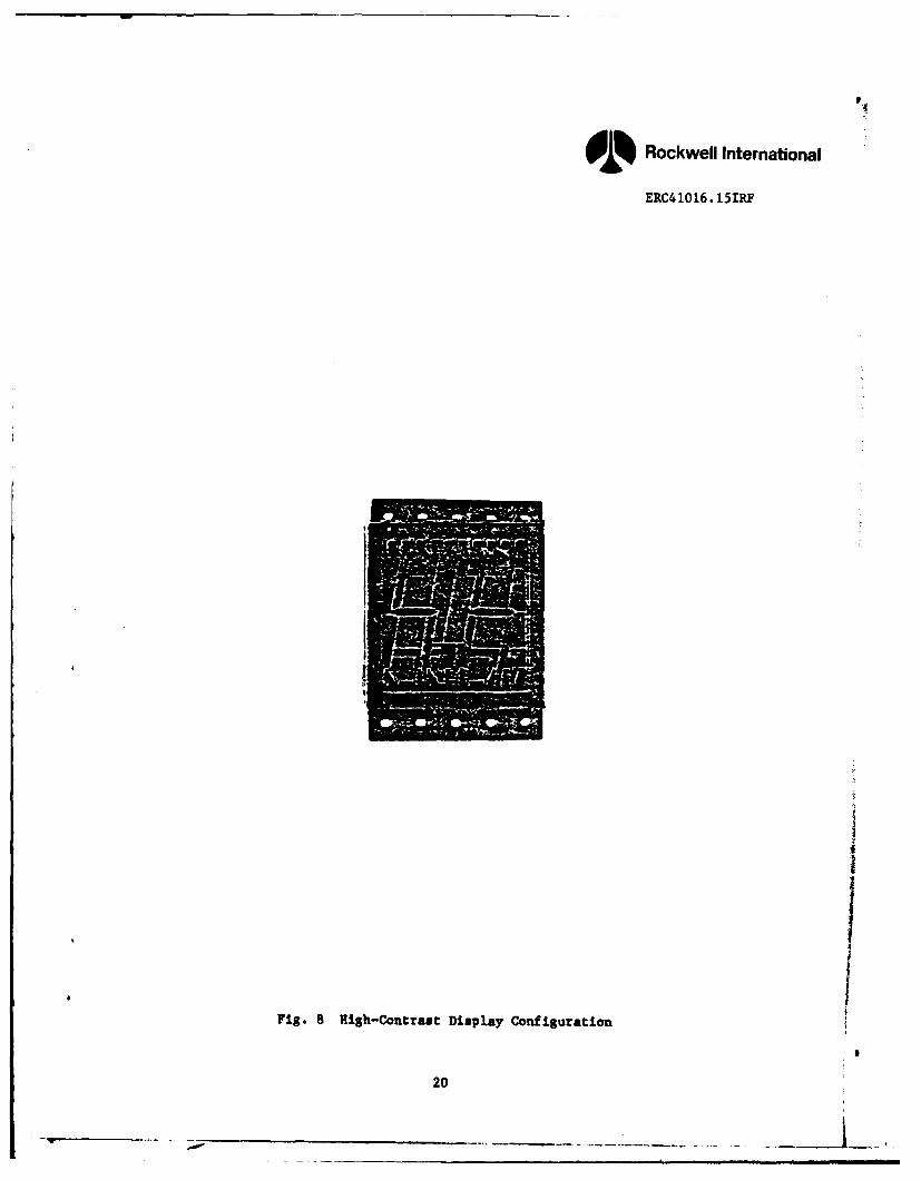
Figure 8 shows a cross sectional view of the display design, showing
the location of the various layers. The active segment areas are defined
by the openings in the light absorbing film. Devices with this structure
have been fabricated and are presently being characterized. Test data will
be reported in the next monthly progress letter.
19
U
91% Rockwell International
ERC41016.15IRF
I
IFig. 8 High-Contrast Display Configuration
20
- , • . . . . .-

9 Rockwell International
ERC41016.15I '
6. HERMETIC SEAL DESIGN AND FABRICATION
6.1 Requirements
The design for the hermetically sealed package for the high-contrast
-FL numeric display with on-board decoder-driver electronics must meet
several requirements:
1. Hermeticity <10- 8 std cc/sec maximum leak rate
2. No organic materials in package
3. Capability of sealing package with controlled atmosphere
4. Must withstand severe military environment
5. Vertical interconnections required to interface drive circuitry
with display
6. Compatibility of sealing process with thin film EL process
7. Conventional socket pin outs and end stackability required
8. Multiplexed digit operation capability.
6.2 Design and Fabrication
Figure 9 shows a cross section of the hermetic seal design. The
design approach utilizes a frit seal to attach the sidewall frame to the
substrate (580*C). The decoder driver electronics are then installed by
conventional die attach and wire bond techniques as shown. Gold wire
thermosonic bonding is used to bond the connections from the IC chips to
the thick film conductor patterns previously applied. The vertical
interconnect bars are then (AuSn) brazed in position (280*C). This assembly
is then brazed to the EL display substrate, simultaneously brazing the
vertical interconnect pads (280*C). Temperature gradients imposed during
the second braze do not allow the connects at the lower ceramic substrate
to raflow.
21
- m Immm-- - - - - m-- - - - - - - -'i m -i m mm

I9
Rockwell International
ERC4 1016. 15IRF
Co M
C,
W, .II U
:
's
Aw
S..
,2
" 2l
2 222
-O ,, .. 025
:.S U UU
• mni m I4I
S -
l I

91% Rockwell International
ERC41016.15IRF
Finally, a controlled atmosphere is introduced in the package through
a porthole in the ceramic substrate. The porthole is sealed by brazing
over with a gold plated Kovar platelet.
The component parts of the package can be seen in Fig. 10. The
substrate and interconnect bars have thick film conductors (PtAu) applied
and the substrate also has a frit material applied for sealing to the
sidewall frame. Figure 11 shows the frit sealed subassembly. The top
surface of the sidewall frame also has a (PtAu) thick film conductor for
use in the final (AuSn) braze seal. All braze seals can be accomplished
in a controlled atmosphere sealing furnace so that fluxes are not required.
Figure 12 shows a sealed package configuration containing the EL display.
The first sealed devices do not yet contain the integrated circuits
as the IC's have not yet been received from the vendor.
Many packages have been assembled with excellent hermeticity
(<10-10 std cc/sec), and reliabe vertical interconnections. Devices with
active EL displays have also been fabricated.
The characteristics of these displays are presently being evaluated,
particularly in the area of operating lifetimes in the hermetically sealed
package. These results will be reported in the near future.
23

9 Rockwell Intemational
ERC41016.15IRF
i4
Fig. 10 Package Component Parts
24

Rockwell International IE1C41016. 15IR7
Fig.11 rritSeaed SbasmbI
25I

ih Rockwell Intemational
ERC4 1016. 15IRF
........-... 5
Ca
XU
C4
(nU
26.

m -
13 November 1979
ELECTRONICS TECHNOLOGY AND DEVICES LABO0RAQ Rockwell International
MANDATORY CONTRACT DISTRIBUTION LIST
101 Defense Technical Information Center 603 Cdr, Atmospheric Sciences LabATTN: DTIC-TCA ERADCOMCameron Station (Bldg 5) ATTN: DELAS-SY-S
012 Alexandria, VA 22314 001 White Sands Missile Range, NM 88002
203 GIDEP Engineering & Support Dept. 607 Cdr, Harry Diamond LaboratoriesTE Section ATTN: DELHD-CO, TD (In Turn)P.O. Box 398 2800 Powder Mill Road
001 NORCO, CA 91760 001 Adelphi, MD 20783
205 Director 609 Cdr, ERADCOMNaval Research Laboratory AT'N: DRDEL-CG, CD, CS (In Turn)ATTN: CODE 2627 2800 Powder Mill Road
001 Washington, DC 20375 001 Adelphi, MD 20783
301 Rome Air Development Center 612 Cdr, ERADCOMATTN: Documents Library (TILD) ATTN: DERDEL-CT
001 Griffiss AFB, NY 13441 2800 Powder Mill Road001 Adelphi, MD 20783
437 Deputy for Science & Technology 0Office, Asst Sec Army (R&D) 680 Commander
001 Washington, DC 20310 US Army Electronics R&D Command000 Fort Monmouth, NJ 07703.438 HQDA (DAMA-ARZ-D/Dr. F. D. Verderame)
001 Washington, DC 20310 1 DELET-0D
482 Director 1 DELSD-L (Tech Library)US Army Material System Analysis Actv 2 OELS-L-S (STINFO)ATTN: DRXSY-T 2 Originating Office
001 Aberdeen Proving Ground, MD 21005 681 Coander
563 Commander, DARCOM US Anrny Comunications R&D CommandATTN: ORCOE ATTN: USMC-LMO5001 Eisenhower Avenue 001 Fort Monmouth, NJ 07703
001 Alexandria, VA 22333 705 Advisory Group on Electron Devices
564 Cdr, US Army Signals Warfare Lab 201 Varick Street, 9th FloorATTN: DELSW-OS 002 New York, NY 10014Vint Hill Farms Station
001 Warrenton, VA 22186
579 Cdr, PM Concept Analysis CentersATTN: DRCP-CACArlington Hall Station
'001 Arlington, VA 22212
602 Cdr, Night Vision & Electro-OpticsERADCOMATTN: DELMV-D
001 Fort Belvoir, VA 22060

e? Rockwell Intemational
ELECTRONICS TECHNOLOGY AND DEVICES LABORATORY
SUPPLEMENTAL CONTRACT DISTRIBUTION LIST(ELECTIVE)
'103 Code R123, Tech Library 477 DirectorDCA Defense Comm Engrg Ctr US Army Ballistic Research Labs1800 Wiehle Ave. ATTN: DRXBR-LB
001 Reston, VA 22090 001 Aberdeen Proving Ground, MD 21005
104 Defense Communications Agency *481 Harry Diamond LaboratoriesTechnical Library Center ATTN: DELHD-RCB (Dr. J. Nemarich)Code 205 (P. A. Tolovi) 2800 Powder Mill Road
001 Washington, DC 20305 001 Adelphi, MD 20783
206 Commander 482 DirectorNaval Electronics Laboratory Center US Army Material Systems Analysis Actv.ATTN: Library ATTN: DRXSY-T, MP (In Turn)
001 San Diego, CA 92152 001 Aberdeen Proving Ground, MD 21005
207 Cdr, Naval Surface Weapons Center 507 Cdr, AVRADCOMWhite Oak Laboratory ATTN: DRSAV-EATTN: Library Code WX-21 P.O. Box 209
001 Silver Spring, MD 20910 001 St. Louis, MO 63166
.314 Hq, Air Force Systems Command 511 Commander, Picatinny ArsenalATTN: OLCA ATTN: SARPA-FR-5, -ND-A-4,Andrews Air Force Base -TS-S (In Turn)
001 Washington, DC 20331 001 Dover, NJ 07801
403 Cdr, MICOM 515 Project Manager, REMBASSRedstone Scientific Info Center ATTN: DRCPM-RBSATTN: Chief, Document Section 001 Fort Monmouth, NJ 07703
001 Redstone Arsenal, AL 35809517 Commander
406 Commandant US Army Satellite Communications AgcyUS Army Aviation Center ATTN: DRCPM-SC-3ATTN: ATZQ-D-MA 001 Fort Monmouth, NJ 07703
001 Fort Rucker, AL 36362518 TRI-TAC Office
407 Director, Ballistic Missile Defense ATTN: TT-SEAdvanced Technology Center 001 Fort Monmouth, NJ 07703ATTN: ATC-R, P.O. Box 1500
001 Huntsville, AL 35807 518 TRI-TAC OfficeATTN: Tr-SE
418 Commander 001 Fort Monmouth, NJ 07703HQ, Fort HuachucaATTN: Technical Reference Division Cdr, US Amy Avionics Lab
001 Fort Huachuca, AZ 85613 AVRADCOMATTN: DAVAA-D
'475 Cdr, Harry Diamond Laboratories 001 Fort Monmouth, NJ 07703ATTN: Library200 Powder Mill Road
001 Adeiphi, MD 20783
*For Millimeter & Microwave Devices Only
-- -"l i a m i I l i m I iiI - -..Owli mm

Rockwell Intemational
SUPPLEMENTAL CONTRACT DISTRIBUTION LIST (ELECTIVE) (CONTINUED)
520 Project Manager, FIREFINDER 619 Cdr, ERADCOMATTN: DRCPM-FF ATTN: DRDEL-PA, -ILS, -ED (In Turn)
001 Fort Monmouth, NJ 07703 2800 Powder Mill Road001 Adelphi, MD 20783
521 CommanderProject Manager, SOTAS .701 MIT - Lincoln LaboratoryATTN: DRCPM-STA ATTN: Library (RM A-082)
001 Fort Monmouth, NJ 07703 P.O. Box 73002 Lexington, MA 02173531 Cdr, US Army Research Office
ATTN: DRXRO-PH (Dr. Lontz) 703 NASA Scientific & Tech Info FacilityDRXRO-IP (In Turn) Baltimore/Washington Intl Airport
P.O. Box 12211 001- P.O. Box 8757, MD 21240001 Research Triangle Park, NC 27709
704 National Bureau of Standards556 HQ, TCATA Bldg 225, Rm A-331
Technical Information Center ATTN: Mr. LeedyATTN: Mrs. Ruth Reynolds 001 Washington, DC 20231Fort Hood, TX 76544
707 TACTEC568 Commander Batelle Memorial Institute
US Army Mobility Eqp Res & Dev Cmd 505.King AvenueATTN: DRDME-R 001 Columbus, OH 43201
001 Fort Belvoir, VA 220604 Reliability Analysis Center604 Chief 001 Griffiss AFB, NY 13441
Ofc of Missile Electronic WarfareElectronic Warfare Lab, ERADCON 001 Mr. Walter Goede
001 White Sands Missile Range, NM 88002 Northrop Corporation2301 W. 120th St.
606 Chief Hawthorne, CA 90250Intel Material Dev & Support OfcElectronic Warfare Lab, ERADCOM
001 Fort Meade, MD 20755
608 CommanderARRADCOMDRDAR-TSB-S
001 Aberdeen Proving Ground, MD 21005
614 Cdr, ERADCOMATTN: DRDEL-LL, -SB, -AP (In Turn)2800 Powder Mill Road
001 Adelphi, MD 20783
617 Cdr, ERADCOMATTN: DRDEL-AQ2800 Powder Mill Road
001 Adelphi, MD 20783
• m

*DAT
FILMED
I0I