mixed-signal multi-level circuit simulation · mixed-signal multi-level circuit simulation...
TRANSCRIPT

EEE / NTU X. ZHOU / 1996
ICCAD Seminar
Mixed-Signal Multi-Level Circuit Simulation
with a Dynamic Delay Model
Dr Zhou Xing
School of Electrical and Electronic EngineeringNanyang Technological University
October 17, 1996
EEE / NTU X. ZHOU / 1996
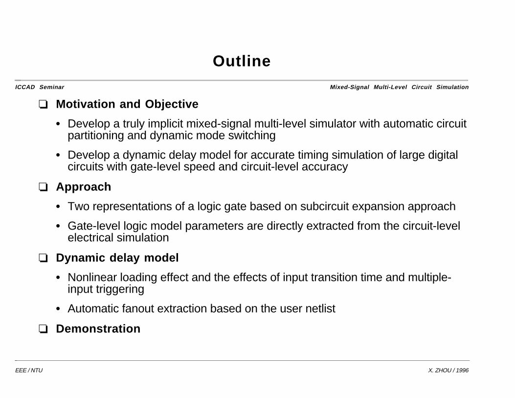
Outline ICCAD Seminar Mixed-Signal Multi-Level Circuit Simulation
❏ Motivation and Objective
• Develop a truly implicit mixed-signal multi-level simulator with automatic circuitpartitioning and dynamic mode switching
• Develop a dynamic delay model for accurate timing simulation of large digitalcircuits with gate-level speed and circuit-level accuracy
❏ Approach
• Two representations of a logic gate based on subcircuit expansion approach
• Gate-level logic model parameters are directly extracted from the circuit-levelelectrical simulation
❏ Dynamic delay model
• Nonlinear loading effect and the effects of input transition time and multiple-input triggering
• Automatic fanout extraction based on the user netlist
❏ Demonstration

EEE / NTU X. ZHOU / 1996
Types of Circuit Simulation ICCAD Seminar Mixed-Signal Multi-Level Circuit Simulation
– “SPICE”– Nodal analysis– Matrix solutions
Circuit Simulation
– Boolean expression– Event driven
Logic Simulation(Digital behavioral modeling)
– Transfer function– Behavioral model
(Analog behavioral modeling)Functional Simulation
Mixed SimulationCombination of two (or more)
types of simulation

EEE / NTU X. ZHOU / 1996
Xsim at a Glance ICCAD Seminar Mixed-Signal Multi-Level Circuit Simulation
❏ Types of simulation
• Electrical (circuit-level) • Mixed signal (analog & digital)
• Digital (gate-level) • Mixed level (gate←circuit→behavioral)
• Analog (behavioral-level) • Mixed technology
❏ Implemented models
• Device models: diode; MOS level 1, 2, 3; BJT Gummel–Poon; AIM HFET,MESFET, HBT, BiCMOS
• Dynamic delay model
• Built-in behavioral functionals (SPICE netlist format)
❏ Key features
• Automatic circuit partitioning
• Dynamic mode switching
• Hierarchical signal probing

EEE / NTU X. ZHOU / 1996
Subcircuit Expansion Approach ICCAD Seminar Mixed-Signal Multi-Level Circuit Simulation
➞
➞

EEE / NTU X. ZHOU / 1996
Logic Block Equivalent Circuit ICCAD Seminar Mixed-Signal Multi-Level Circuit Simulation
Vlogic(t)
D/A
ThresholdDetector
A/D
Digital Out
Digital In
Analog InLogic Gate
Back-enddelay
Analog Out
Vout(t)=Vlogic(t+delay)
R
+–
A Q = A

EEE / NTU X. ZHOU / 1996
The Need for a Dynamic Delay Model ICCAD Seminar Mixed-Signal Multi-Level Circuit Simulation
❏ Fanout
• Delay depends on theload, which is non–linear for submicroncircuits
• User-netlistdependent
❏ Input slope
• Delay depends on theinput transition time(slope)
• Run-time dependent
❏ Fanin
• For multiple inputgate, delay dependson which input istriggered
• Run-time dependent
Del
ay
Capacitive Load
Del
ay
Capacitive Load
Timax
Timin
Del
ay
Capacitive Load
all input
single input

EEE / NTU X. ZHOU / 1996
Logic Gate Model ICCAD Seminar Mixed-Signal Multi-Level Circuit Simulation
❏ Logic element
U1 0 3 2 1 hfet nor2 hfet-nor2➀
➁➂U1
❏ Logic (digital, behavioral) representation
.model hfetnor2 logic vmax=1.0 + vmin=0.1 thh=0.8 thl=0.2 mr=5 + mf=5 over=0.1 cap1=… cap2=…
Cout
Q
A
BCinA
CinB
❏ Circuit (analog, structural) representation
.subckt hfet-nor2 0 3 2 1 A1 3 1 0 nhfet l=0.5u w=5u A2 3 2 0 nhfet l=0.5u w=5u A3 4 3 3 nhfet l=0.5u w=4u Vdd 4 0 1.0 .ends
Vdd
A1
A3
A2➁➀
➂
➃
A
B
Q

EEE / NTU X. ZHOU / 1996
Basic Logic Gate Parameters ICCAD Seminar Mixed-Signal Multi-Level Circuit Simulation
❏ Input capacitance
• Cin = ⟨ ⟩I(V)dV/dt
V
❏ Intrinsic delay• tdi = td CL = 0
❏ Effective resistance
• Reff = td – tdi
CL
❏ Output capacitance
• Cout = ⟨ ⟩tdiReff
rise,fall
❏ Rise and fall times
• tr = tri + RtrCL• tf = tfi + RtfCL
CinA
CinB
Cout
A
B
Q
CL
➝ ➝
➝ ➝
➝
➝
➝
➝
tdrtdf
t rt f
td = td i + R effC L

EEE / NTU X. ZHOU / 1996
Fanout (Loading Capacitance) Extraction ICCAD Seminar Mixed-Signal Multi-Level Circuit Simulation
Trace all the logic gates and grounding capacitances
C0
Cout
C in
C in
U1
U2
U3
C fanout = C 0 + ∑U
C in + ∑U
Cout

EEE / NTU X. ZHOU / 1996
How to Handle Nonlinear Load Dependence ICCAD Seminar Mixed-Signal Multi-Level Circuit Simulation
Piece-wise linear approximation
❏ N-breakpoint algorithm
• Run full-subcircuit for N loadingcapacitances to extract thedelays
• Store the delay parameters inthe logic model
❏ Linear interpolation (orextrapolation) betweenneighboring breakpoints
Del
ay
C4LC2
L C3L
Capacitive LoadCfanout
td
tdi
Reff
C1L

EEE / NTU X. ZHOU / 1996
How to Handle Input Slope Dependence ICCAD Seminar Mixed-Signal Multi-Level Circuit Simulation
Linear interpolation/extrapolation
❏ Max/min slope pre-calculation
• Run full-subcircuit for two“extreme” input transition timesto extract the delays
• Store the delay parameters inthe logic model
❏ Linear interpolation/extrapolation
• Trace the input transition time ateach time step for each gate
• Use linear interpolation based onthe actual Cfanout and itsinterpolated values betweenneighboring breakpoints
Ti min
Timax
Ti
Del
ay
Capacitive LoadCfanout
td Ti max
Ti min
C4LC2
L C3LC1
L
EEE / NTU X. ZHOU / 1996
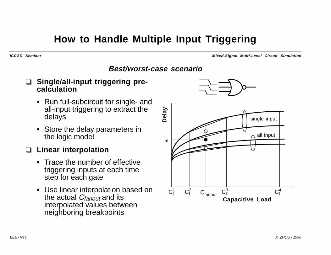
How to Handle Multiple Input Triggering ICCAD Seminar Mixed-Signal Multi-Level Circuit Simulation
Best/worst-case scenario
❏ Single/all-input triggering pre-calculation
• Run full-subcircuit for single- andall-input triggering to extract thedelays
• Store the delay parameters inthe logic model
❏ Linear interpolation
• Trace the number of effectivetriggering inputs at each timestep for each gate
• Use linear interpolation based onthe actual Cfanout and itsinterpolated values betweenneighboring breakpoints
td
Del
ay
Capacitive LoadCfanout C4
LC2L C3
LC1L
single input
all input
EEE / NTU X. ZHOU / 1996
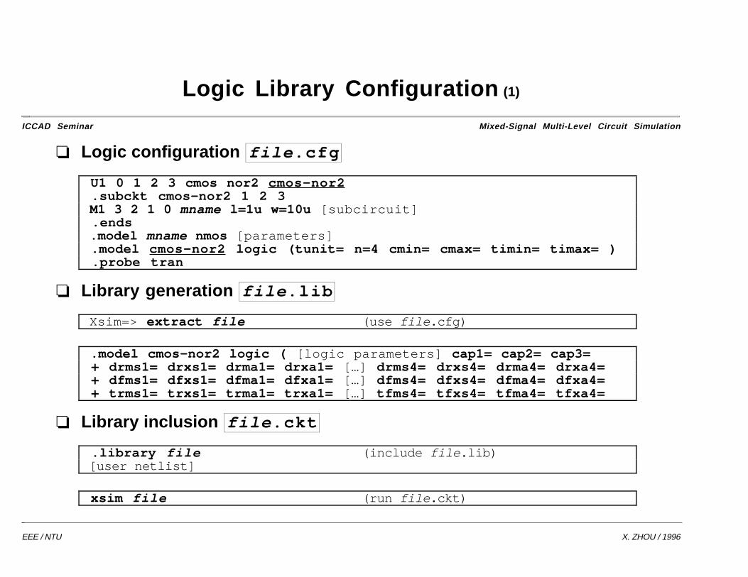
Logic Library Configuration (1) ICCAD Seminar Mixed-Signal Multi-Level Circuit Simulation
❏ Logic configuration file.cfg
U1 0 1 2 3 cmos nor2 cmos-nor2 .subckt cmos-nor2 1 2 3 M1 3 2 1 0 mname l=1u w=10u [subcircuit] .ends .model mname nmos [parameters] .model cmos-nor2 logic (tunit= n=4 cmin= cmax= timin= timax= ) .probe tran
❏ Library generation file.lib
Xsim=> extract file (use file.cfg)
.model cmos-nor2 logic ( [logic parameters] cap1= cap2= cap3= + drms1= drxs1= drma1= drxa1= […] drms4= drxs4= drma4= drxa4= + dfms1= dfxs1= dfma1= dfxa1= […] dfms4= dfxs4= dfma4= dfxa4= + trms1= trxs1= trma1= trxa1= […] tfms4= tfxs4= tfma4= tfxa4=
❏ Library inclusion file.ckt
.library file (include file.lib) [user netlist]
xsim file (run file.ckt)

EEE / NTU X. ZHOU / 1996
Logic Library Configuration (2) ICCAD Seminar Mixed-Signal Multi-Level Circuit Simulation
cap1cap2
cap3
t dr
C4LC2
L C3LC1
L
single input
all input
timin
timax
timintimax
cmin cmax
t rt df t f
drms3
dfxs4
trma3
tfxa2

EEE / NTU X. ZHOU / 1996
Input Capacitance Determination ICCAD Seminar Mixed-Signal Multi-Level Circuit Simulation
0
2
4
6
8
10
0
Inpu
t C
apac
itanc
e (f
F)
1Input Voltage (V)
Input capacitanceAveraged capacitance

EEE / NTU X. ZHOU / 1996
Delay with Different Input Transition Times ICCAD Seminar Mixed-Signal Multi-Level Circuit Simulation
0
10
20
30
40
50
Del
ay (
ps)
0 10 20 30 40
Input transition time (ps)
Loading Capacitance (fF)
0.5
5
10

EEE / NTU X. ZHOU / 1996
Delay with Multiple Input Triggering ICCAD Seminar Mixed-Signal Multi-Level Circuit Simulation
0
10
20
30
40
50
60
70
Del
ay (
ps)
0 10 20 30 40Loading Capacitance (fF)
Rise delay
Fall delay
(best)
(worst)
(worst)
(best)

EEE / NTU X. ZHOU / 1996
Fanout Extraction and Subcircuit Tracing (1) ICCAD Seminar Mixed-Signal Multi-Level Circuit Simulation
C1
U1 U2 U3 U4
U5
U6
U7
➀ ➁ ➂ ➃ ➄
➆
➅
➇
A1
A2In
Out
VddW/L
Xsim netlist .lib hfet U1 0 2 1 hfet inv1 hfet-inv1 U2 0 3 2 hfet inv1 hfet-inv1 U3 0 4 3 hfet inv1 hfet-inv1 U4 0 5 4 hfet inv1 hfet-inv1 U5 0 6 2 hfet inv2 hfet-inv2 U6 0 7 2 hfet inv3 hfet-inv3 U7 0 8 2 hfet inv4 hfet-inv4 C1 0 5 5e-15 V1 1 0 pulse(1. 0. 0. 10p 10p + 100p 200p) .ic v(5)=0 .set mode=analog *.set mode=digital .probe tran v(nodes) .plot tran v 2 5 .tran 0 400p 1p

EEE / NTU X. ZHOU / 1996
Fanout Extraction and Subcircuit Tracing (2) ICCAD Seminar Mixed-Signal Multi-Level Circuit Simulation
Xsim=> fanout U1: c_fanout = 1.93372e-14 U2: c_fanout = 6.1576e-15 U3: c_fanout = 6.1576e-15 U4: c_fanout = 6.67485e-15 U5: c_fanout = 2.01527e-15 U6: c_fanout = 2.11913e-15 U7: c_fanout = 1.63416e-15Xsim=> network uNode: Branches: 0: U1 U2 U3 U4 U5 U6 U7 1: U1 2: U1 U2 U5 U6 U7 3: U2 U3 4: U3 U4 5: U4 6: U5 7: U6 8: U7Xsim=> network aNode: Branches: 0: A1.U1 A1.U2 A1.U3 A1.U4 A1.U5 A1.U6 A1.U7 1: A1.U1 2: A2.U1 A2.U1 A1.U1 A1.U2 A1.U5 A1.U6 A1.U7 3: A2.U2 A2.U2 A1.U2 A1.U3 4: A2.U3 A2.U3 A1.U3 A1.U4 5: A2.U4 A2.U4 A1.U4 6: A2.U5 A2.U5 A1.U5 7: A2.U6 A2.U6 A1.U6 8: A2.U7 A2.U7 A1.U7
Xsim=> network cNode: Branches: 0: C1 1: Cgd.A1.U1 Cgs.A1.U1 2: Cgd.A2.U1 Cgs.A2.U1 Cgd.A1.U2+ Cgs.A1.U2 Cgd.A1.U5 Cgs.A1.U5+ Cgd.A1.U6 Cgs.A1.U6 Cgd.A1.U7+ Cgs.A1.U7 3: Cgd.A2.U2 Cgs.A2.U2 Cgd.A1.U3+ Cgs.A1.U3 4: Cgd.A2.U3 Cgs.A2.U3 Cgd.A1.U4+ Cgs.A1.U4 5: Cgd.A2.U4 Cgs.A2.U4 C1 6: Cgd.A2.U5 Cgs.A2.U5 7: Cgd.A2.U6 Cgs.A2.U6 8: Cgd.A2.U7 Cgs.A2.U7Xsim=> network rNode: Branches: 0: Rs.A1.U1 Rs.A1.U2 Rs.A1.U3+ Rs.A1.U4 Rs.A1.U5 Rs.A1.U6 Rs.A1.U7 1: 2: Rs.A2.U1 Rd.A1.U1 3: Rs.A2.U2 Rd.A1.U2 4: Rs.A2.U3 Rd.A1.U3 5: Rs.A2.U4 Rd.A1.U4 6: Rs.A2.U5 Rd.A1.U5 7: Rs.A2.U6 Rd.A1.U6 8: Rs.A2.U7 Rd.A1.U7

EEE / NTU X. ZHOU / 1996
Comparison of Different Delay Models ICCAD Seminar Mixed-Signal Multi-Level Circuit Simulation
0.0
0.2
0.4
0.6
0.8
1.0
1.2
Vol
tage
at
Nod
e 2
(V)
0 50 100 150 200 Time (ps)
Full-circuit
Dynamic-delay
Unit-delay
Zero-delay
0.0
0.2
0.4
0.6
0.8
1.0
1.2
100
Vol
tage
at
Nod
e 5
(V)
150 200 250 300 Time (ps)
Full-circuit
Dynamic-delay
Unit-delay
Zero-delay
• Circuit parameters: W1–4 = 5 µm, W5 = 4 µm, W6 = 6 µm, W7 = 7 µm
• Input capacitances: Cin1–4 = 4.48 fF, Cin5 = 4.64 fF, Cin6 = 4.33 fF, Cin7 = 4.20 fF
• CPU time (sec): Full-circuit = 21.86, dynamic = 3.89, unit = 3.61, zero = 3.54

EEE / NTU X. ZHOU / 1996
Multi-Level Modeling of Logic Gates ICCAD Seminar Mixed-Signal Multi-Level Circuit Simulation
Multi-level representation of an HEMT
DGS
D
G
SIn Out
Device Gate
D
G
S ➝
➝
Transistor Circuit
In
Out
+
Device Level Transistor Level Gate Level
.model <Mname> nhfet+ [param-list]
Axxx <Nd> <Ng> <Ns>+ <Mname> <L=val> <W=val>
Uxxx <Nref> <Nout> <Nin1>+ [<Nin2> …] <Family>+ <Type><n> <Cktname>

EEE / NTU X. ZHOU / 1996
Transistor-Level DC Characteristics ICCAD Seminar Mixed-Signal Multi-Level Circuit Simulation
HEMT device with L = 1 µm, W = 10 µm
Output Characteristic Input Characteristic
0.0
0.2
0.4
0.6
0.8
0.0
Dra
in C
urre
nt (
mA
)
0.2 0.4 0.6 0.8 1.0
Vgs = 0.6V
0.5V
0.4V
Drain-Source Voltage (V)
SimulationExperiment
0.3V
10-1410-1310-1210-1110-10
Dra
in C
urre
nt (
mA
)
10-910-810-710-610-5 Vds = 1V10-410-3
Gate-Source Voltage (V)
10-2
-0.5 0.0 0.5 1.0
0.01V

EEE / NTU X. ZHOU / 1996
Gate-Level Timing Simulation ICCAD Seminar Mixed-Signal Multi-Level Circuit Simulation
Seven-stage NOR-gate ring oscillator using E/D HEMT device
Circuit Waveform
➂➀
➁
➃ ➄
➅➆➇
U1 U2 U3
U4
U5U6U7
C2C1 C3
C4
CPU Time
Digital mode: 12.85 sec
Analog mode: 57.43 sec
-0.5
0.0
0.5
1.0
1.5
V2
(V)
Analog Digital
-0.5
0.0
0.5
1.0
1.5
0
V3
(V)
100 200 300 400 500 600
Analog
Time (ps)
Digital

EEE / NTU X. ZHOU / 1996
Multi-Level Digital Simulation (1) ICCAD Seminar Mixed-Signal Multi-Level Circuit Simulation
21
D Q
Q_
22
D Q
Q_
23
D Q
Q_
Clock
24
D Q
Q_
U4
U3
U2
U1
U5
U6
Preset
Clock
Data
Clear
Q
QB
DFF
➤
➤ ➤ ➤
➤
➤
A
B
C
Output
Vdd
M1
M2
M3
M4 M5 M6
NAND3
EEE / NTU X. ZHOU / 1996
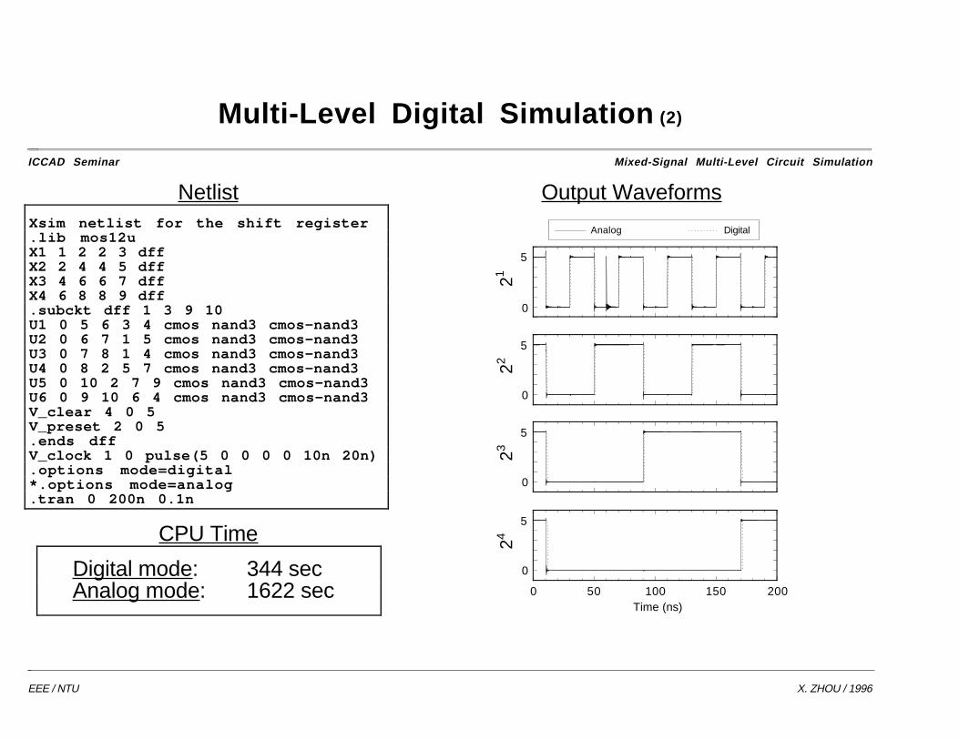
Multi-Level Digital Simulation (2) ICCAD Seminar Mixed-Signal Multi-Level Circuit Simulation
Netlist Output WaveformsXsim netlist for the shift register.lib mos12uX1 1 2 2 3 dffX2 2 4 4 5 dffX3 4 6 6 7 dffX4 6 8 8 9 dff.subckt dff 1 3 9 10U1 0 5 6 3 4 cmos nand3 cmos-nand3U2 0 6 7 1 5 cmos nand3 cmos-nand3U3 0 7 8 1 4 cmos nand3 cmos-nand3U4 0 8 2 5 7 cmos nand3 cmos-nand3U5 0 10 2 7 9 cmos nand3 cmos-nand3U6 0 9 10 6 4 cmos nand3 cmos-nand3V_clear 4 0 5V_preset 2 0 5.ends dffV_clock 1 0 pulse(5 0 0 0 0 10n 20n).options mode=digital*.options mode=analog.tran 0 200n 0.1n
CPU Time
Digital mode: 344 secAnalog mode: 1622 sec
0
5
21
Analog Digital
0
5
220
5
23
0
524
Time (ns)0 50 100 150 200

EEE / NTU X. ZHOU / 1996
Circuit-Level Behavioral Modeling ICCAD Seminar Mixed-Signal Multi-Level Circuit Simulation
x yf(x)
❏ Idea — model circuit elements using functions
❏ Netlist syntax
• SPICE format: Label connection value/function
e.g., R1 1 2 10K Vin 3 0 sin(2.5 0.1 10meg)
• Xsim extension: Label connection expression
where expressions: value; function + conditionals; sum of functions

EEE / NTU X. ZHOU / 1996
Built-in Behavioral Modeling Functions and Conditionals ICCAD Seminar Mixed-Signal Multi-Level Circuit Simulation
❏ Built-in functions
exp cornerdown maxpulse cornerup netfunctionpwl complex notchsffm delay offsetsin expterm polartanh generator polyterm
❏ Conditionals
ac tran frequencydc period timedctran
❏ Some examples
x
f(x)notch
x
f(x)max
x
f(x)offset
x
f(x)corner
up
x
f(x)cornerdown

EEE / NTU X. ZHOU / 1996
Op-Amp Macromodel (1) ICCAD Seminar Mixed-Signal Multi-Level Circuit Simulation
Schematic Netlist
~
–
+
Vin
RT1
RT2
out
➞
➞
+
–
➞ +
–
in-
in+
IA
IB
RIA
RIC
RIB
E2
CP
RP
G1 R1 E1
YoC1
out
* Xsim netlist for op-amp macromodel Xop_amp3 5 1 3 op_amp .subckt op_amp 9 8 1 Yo 3 1 max(0.02 0.02) E1 3 0 0 4 max(505 13) C1 4 3 30p R1 4 0 3meg G1 4 0 0 6 tanh(185u 19u) CP 6 0 1p RP 7 6 150k E2 7 0 8 9 1 RIC 0 10 100meg RIB 9 10 1meg RIA 8 10 1meg IB 9 0 80n IA 8 0 80n .ends op_amp Vin 5 0 pwl(0 0 10u 0 10.1u -1 40u + -1 40.1u 1 100u 1) ac (1) RT2 0 1 1k RT1 1 3 ac (100G) tran (100k) .plot ac vdb 3 .plot ac vp 3 .plot tr v 5 .plot tr v 3 .tran 0 100u 1u .ac 1 1e7 dec 10

EEE / NTU X. ZHOU / 1996
Op-Amp Macromodel (2) ICCAD Seminar Mixed-Signal Multi-Level Circuit Simulation
Transient Response AC Response
-15
-10
-5
0
5
10
15
Vol
tage
(V
)
0 20 40 60 80 100
Vin
Vout
Time (µs)
-100
0
100
200
Vol
tage
at O
utpu
t (dB
)
-200
-150
-100
-50
0
100
Pha
se a
t O
utpu
t (d
egre
e)102 104 106
Frequency (Hz)

EEE / NTU X. ZHOU / 1996
Switched-Capacitor Filter (1) ICCAD Seminar Mixed-Signal Multi-Level Circuit Simulation
Complete Circuit Behavioral Model
M1 M2
V1 V2
C1
C2Vin
➃
~
C1
C2Vin
Y2Y1➀
~
* Xsim netlist for complete circuit Vin 6 0 sin(0 1 100k 0 0) V1 1 0 pulse(5 0 0 0 0 500n 1u) V2 7 0 pulse(0 5 0 0 0 500n 1u) C1 6 5 1p C2 4 0 1p M1 5 1 4 4 nnn l=100u w=100u M2 4 7 0 0 nnn l=100u w=100u .model nnn nmos (level=2 vto=1) .plot tr v 4 .tran 0 20u 0.1u .status .clear
* Xsim netlist for behavioral model Vin 7 0 sin(0 1 100k 0 0) C1 7 3 1p C2 1 0 1p Y1 3 1 period(1u) (20u) time(500n) (0) Y2 1 0 period(1u) (0) time(500n) (20u) .generator freq=100k .plot tr v 1 .tran 0 20u 0.1u .status .end

EEE / NTU X. ZHOU / 1996
Switched-Capacitor Filter (2) ICCAD Seminar Mixed-Signal Multi-Level Circuit Simulation
Complete Circuit Behavioral Model
-0.5
0
0.5
0 5 10 15
Vol
tage
at
Nod
e 4
(V)
20
Time (µs)
-0.5
0
0.5
0 5 10 15
Vol
tage
at
Nod
e 1
(V)
20
Time (µs)
CPU: 0.69 sec. CPU: 0.18 sec.

EEE / NTU X. ZHOU / 1996
8th-Order Chebyshev Filter (1dB Ripple) (1) ICCAD Seminar Mixed-Signal Multi-Level Circuit Simulation
Lumped Circuit Behavioral Model
~
L1 L2 L3 L4
C1 C2 C3 C4RL
Vin
➁ +
–~ Vin E1
+
–
➀
* Xsim netlist for lumped circuit RL 0 2 1k C4 2 0 173.033n C3 3 0 326.857n C2 4 0 341.435n C1 5 0 332.984n L4 2 3 234.769m L3 3 4 268.176m L2 4 5 270.899m L1 5 6 217.899m Vin 6 0 ac 1 .plot ac vdb 2 .plot ac vp 2 .ac 100 1000 dec 100
* Xsim netlist for behavioral model E1 1 0 3 0 netfunction(1 1k 8 0.017227 + 0.107345 0.447826 0.846824 1.836902 + 1.655156 2.423026 0.919811 1 + 0.017227) Vin 3 0 ac 1 .plot ac vdb 1 .plot ac vp 1 .ac 100 1000 dec 100

EEE / NTU X. ZHOU / 1996
8th-Order Chebyshev Filter (1dB Ripple) (2) ICCAD Seminar Mixed-Signal Multi-Level Circuit Simulation
Lumped Circuit Behavioral Model
0
0.5
1
102 103
-200
-100
0
100
200
Vol
tage
at
Nod
e 2
(dB
)
-200
-100
0
100
200
102Pha
se a
t N
ode
2 (d
egre
e)
103 104
Frequency (Hz)
0
0.5
1
102 103
-200
-100
0
100
200
Vol
tage
at
Nod
e 1
(dB
)
-200
-100
0
100
200
102
Pha
se a
t N
ode
1 (d
egre
e)
103 104
Frequency (Hz)

EEE / NTU X. ZHOU / 1996
Implicit Mixed-Mode Simulation ICCAD Seminar Mixed-Signal Multi-Level Circuit Simulation
~
➀ ➁
Vin
➂
Mode CPU (sec.)
Analog 3.57
Digital 0.82
Mixed 2.45 (30% speedup)
In mixed mode:
• U1 switched to digital after 1.86 µs
• U2 and U3 switched to digital after0.45 µs
-10
12
3
45
6
Vin
-10
12
3
45
6
v(1)
-10
12
3
45
6
v(2)
-10
12
3
45
6
v(3)
0 0.5 1 1.5 2Time (µs)

EEE / NTU X. ZHOU / 1996
Mixed-Mode Phase-Locked Loop (1) ICCAD Seminar Mixed-Signal Multi-Level Circuit Simulation
~PD VCO
Vss
C1
R2
R1
Vdd
Out
VREF
Int
➤
INref
INfb
U1
U2
U3 M10
PRD
Vss
Vdd
OUT
PD
➤
➤
➞➞
+
–
M3
M6
GSOURCE
GSINK
RSINK
RSOURCE
Control
Output
Ro
EO
RP1
RP2
RI
RF2C2
Vdd
Vss Gnd
Int VCO

EEE / NTU X. ZHOU / 1996
Mixed-Mode Phase-Locked Loop (2) ICCAD Seminar Mixed-Signal Multi-Level Circuit Simulation
Xsim PLL netlist* Phase detectorX2 1 2 3 31 32 PD* VCOX1 4 2 31 32 0 40 VCO* Low pass filterR1 3 4 1MegC1 4 9 3nR2 9 32 100K* Clock referenceV1REF 1 0 pulse(0 5 0 20u 20u 60u 0.0012)* Power suppliesVDD 31 0 dc ( 5)VSS 32 0 dc (-5)*** Phase Detector SubCkt **** Input(1) Input(2) Output(6) VDD(7) VSS(8).subckt PD 1 2 6 7 8U1 0 3 1 2 cmos nand2 cmos-nand2U2 0 4 1 2 cmos or2 cmos-or2U3 0 5 3 4 cmos nand2 cmos-nand2M10 6 5 7 7 pmos l=2u w=50u ad=20p as=20p pd=24u+ ps=24uRPD 6 8 10K.ends*** VCO Subckt **** Control(33) Output(5) VDD(31) VSS(32)* Gnd(10) Int(6).subckt VCO 33 5 31 32 10 6* Comparator with hysteresis* -input(1) +input(6) output(5) gnd(10)* Op-amp model: AVo~277K RI=2Meg RO=50 Vo=+/-5V
RI 1 2 20MegRo 4 5 50E1 4 10 2 1 max(25K 5)* Feedback elements for hysteresisRF2 1 10 1RP1 5 2 4MegRP2 2 6 1Meg* Charge element for currentC2 6 10 100n* Transconductance and current steering stageRSINK 32 35 10MegRSORCE 36 31 10MegGSORCE 31 36 33 32 110uGSINK 35 32 33 32 110uM3 6 5 35 32 nmos l=2u w=20u ad=20p as=20p pd=24u+ ps=24uM6 6 5 6 31 pmos l=2u w=40u ad=20p as=20u pd=24u+ ps=24u.ends* Analysis.lib pll.IC v(40)=-1.options mode=analog itl4=500.plot tran v(1) v(2) v(3) v(4) v(40).probe tran vdsb M6.X1.probe tran idsb M6.X1.probe tran vdsb M3.X1.probe tran idsb M3.X1.tran 0 19m 0.01m.status.end

EEE / NTU X. ZHOU / 1996
Mixed-Mode Phase-Locked Loop (3) ICCAD Seminar Mixed-Signal Multi-Level Circuit Simulation
Transient Response Internal Probe
-6
-4
-2
0
2
4
6
Vol
tage
(V
)
0 5 10 15 20
Vref
Time (ms)
v(1) v(2) v(4)
VCO(out) LF(out)
-0.2
0
0.2
0.4
0.6
0.8
1
1.2
M3
Sub
stra
te D
iode
Cur
rent
(m
A)
0 5 10 15 20
Time (ms)

EEE / NTU X. ZHOU / 1996
Xsim: Applications ICCAD Seminar Mixed-Signal Multi-Level Circuit Simulation
❏ Large digital circuits
• Using full “digital” mode for logic synthesis with vendor-supplied delayparameters, and then, subcircuit model for back-annotated timing verification
❏ Mixed-signal interface circuits
• Using “mixed” mode for data-converter systems with large ratio ofdigital/analog circuitry
❏ PCB-level system simulation
• Large systems with mixed digital (including mixed logic families) and analogfunctional blocks