mixed-signal circuit simulator · ii p-cad mixed-signal circuit simulator user’s guide specifying...
TRANSCRIPT
Mixed-Signal Circuit Simulator

Copyrights
Software, documentation and related materials: Copyright © 2002 Altium Limited
This software product is copyrighted and all rights are reserved. The distribution and sale of this product are intended for the use of the original purchaser only per the terms of the License Agreement.
This document may not, in whole or part, be copied, photocopied, reproduced, translated, reduced or transferred to any electronic medium or machine-readable form without prior consent in writing from Altium Limited.
U.S. Government use, duplication or disclosure is subject to RESTRICTED RIGHTS under applicable government regulations pertaining to trade secret, commercial computer software developed at private expense, including FAR 227-14 subparagraph (g)(3)(i), Alternative III and DFAR 252.227-7013 subparagraph (c)(1)(ii).
P-CAD is a registered trademark and P-CAD Schematic, P-CAD Relay, P-CAD PCB, P-CAD ProRoute, P-CAD QuickRoute, P-CAD InterRoute, P-CAD InterRoute Gold, P-CAD Library Manager, P-CAD Library Executive, P-CAD Document Toolbox, P-CAD InterPlace, P-CAD Parametric Constraint Solver, P-CAD Signal Integrity, P-CAD Shape-Based Autorouter, P-CAD DesignFlow, P-CAD ViewCenter, Master Designer and Associate Designer are trademarks of Altium Limited. Other brand names are trademarks of their respective companies.
Altium Limited www.altium.com

P-CAD Mixed-Signal Circuit Simulator User’s Guide i
Table of Contents
chapter 1 Introduction About this Guide..................................................................................................................1 Installation and Setup..........................................................................................................2
System Requirements ..................................................................................................2 Installing P-CAD Products............................................................................................2
Introduction to the P-CAD Mixed-Signal Circuit Simulator...................................................3
chapter 2 Working in the Design Explorer The Technology inside Design Explorer ..............................................................................6
What is the Design Explorer?.......................................................................................6 What is a Design Database?........................................................................................7
Using the Design Explorer...................................................................................................8 Using the Navigation Panel ..........................................................................................8 Working in the Integrated Design Window ...................................................................9
Managing documents in the Design Database ..................................................................11 Using folders to create a hierarchy.............................................................................11 Moving, copying and deleting documents ..................................................................12 Renaming a document or folder .................................................................................12
chapter 3 Getting Started with Simulation Creating the circuit ............................................................................................................13 Adding the Source Components........................................................................................14 Defining the points to be plotted ........................................................................................14 Setting up the Analyses.....................................................................................................14 Running a simulation.........................................................................................................14 Viewing the simulation results ...........................................................................................15
chapter 4 Setting up and Running a Simulation Setting up a simulation run ................................................................................................17 Running a simulation from the Schematic design..............................................................18 Running a simulation directly from the Circuit Simulator ...................................................19 Specifying the simulation data...........................................................................................20
Specifying simulation data to be collected..................................................................20
ii P-CAD Mixed-Signal Circuit Simulator User’s Guide
Specifying simulation data to be displayed................................................................ 21 Selecting Analyses to run ................................................................................................. 22
Transient Analysis ..................................................................................................... 22 AC Small Signal Analysis (AC Sweep) ...................................................................... 24 DC Sweep Analysis ................................................................................................... 26 DC Operating Point Analysis ..................................................................................... 28 Monte Carlo Analysis................................................................................................. 29 Parameter Sweep...................................................................................................... 33 Temperature Sweep .................................................................................................. 35 Fourier Analysis......................................................................................................... 36 Transfer Function Analysis ........................................................................................ 37 Noise Analysis ........................................................................................................... 38 Impedance Plot Analysis ........................................................................................... 39
Mathematical Functions and Waveforms.......................................................................... 40 Modifying the SPICE netlist for a simulation ..................................................................... 43 Identifying simulation circuit nodes ................................................................................... 44 Setting initial conditions for simulation .............................................................................. 44
chapter 5 The Waveform Analysis Window Displaying waveforms....................................................................................................... 48 Resizing the waveforms.................................................................................................... 48 Viewing waveforms in separate cells ................................................................................ 50 Displaying multiple waveforms in the same cell................................................................ 51 Displaying a waveform scaled two ways........................................................................... 51 Scaling the Waveforms’ Axes ........................................................................................... 52
Setting the scale type ................................................................................................ 52 Displaying the simulation data points................................................................................ 53 Identifying waveforms on a single color printout ............................................................... 53 Using the Measurement Cursors ...................................................................................... 54
How multi-pass results are displayed ........................................................................ 55
chapter 6 Voltage and Current Sources Constant (DC) simulation sources .................................................................................... 57 Sinusoidal source ............................................................................................................. 58 Periodic Pulse source ....................................................................................................... 60 Piece-Wise-Linear source................................................................................................. 62 Exponential sources ......................................................................................................... 64 Frequency Modulation source .......................................................................................... 66 Linear Dependent sources................................................................................................ 68 Non-linear Dependent sources ......................................................................................... 69 F/V Converter simulation source....................................................................................... 70 VCO simulation source ..................................................................................................... 71
chapter 7 Components and Models Selecting simulation-ready components ........................................................................... 73
Models and Subcircuits ............................................................................................. 74 Device Descriptions................................................................................................... 74

P-CAD Mixed-Signal Circuit Simulator User’s Guide iii
Simulation-ready Resistors................................................................................................74 Simulation-ready Capacitors .............................................................................................75 Simulation-ready Inductors................................................................................................76 Simulation-ready Diodes ...................................................................................................76 Simulation-ready BJTs ......................................................................................................77 Simulation-ready JFETs ....................................................................................................78 Simulation-ready MOSFETs..............................................................................................78 Simulation-ready MESFETs ..............................................................................................80 Simulation-ready V/I Controlled Switches..........................................................................80 Simulation-ready Transmission Lines................................................................................81 Simulation-ready Transformers .........................................................................................83 Simulation-ready Fuses.....................................................................................................83 Simulation-ready Crystals..................................................................................................83 Simulation-ready Relays....................................................................................................84 Simulation-ready integrated components ..........................................................................85 Simulation-ready TTL and CMOS logic components.........................................................85
chapter 8 Creating your own simulation-ready components Simulation Attributes - SimType ........................................................................................87 Simulation Attributes - SimModel ......................................................................................89 Simulation Attributes - SimFile ..........................................................................................90 Simulation Attributes - SimPins .........................................................................................90 Simulation Attributes - SimNetlist ......................................................................................91 Simulation Attributes - SimDefaults ...................................................................................93 Simulation Attributes - SimField1-16 .................................................................................93
chapter 9 Troubleshooting simulation problems Simulation netlist cannot be created..................................................................................95 Simulation analysis failures ...............................................................................................96 General simulation convergence troubleshooting..............................................................96 DC Sweep analysis troubleshooting..................................................................................97 Transient Analysis troubleshooting....................................................................................98
chapter 10 SPICE Variables and Analog Options Setting up advanced simulation options ............................................................................99 Suggested SPICE Reading .............................................................................................104
chapter 11 Simulating Digital Designs Creating new SimCode devices ......................................................................................107
Creating symbols for digital simulation parts ............................................................108 Defining property fields for a digital simulation part ..................................................108 Creating the model linking file for a digital simulation part........................................109 Creating a SimCode digital device simulation model ...............................................111 Creating a compiled SimCode model file .................................................................111 SimCode digital simulation model example..............................................................111
SimCode Language Reference .......................................................................................114
iv P-CAD Mixed-Signal Circuit Simulator User’s Guide
SimCode statement termination character .............................................................. 114 Beginning a SimCode model definition.................................................................... 115 Including comments in SimCode files...................................................................... 115
SimCode Language Definition ........................................................................................ 115 SimCode language syntax.............................................................................................. 118
# xxxx source (SimCode function) ........................................................................... 118 CHANGE_TIME (SimCode function) ....................................................................... 119 CHANGED_xx (SimCode function) ......................................................................... 119 DELAY (SimCode function) ..................................................................................... 120 DRIVE (SimCode function) ...................................................................................... 121 EVENT (SimCode function) ..................................................................................... 123 EXIT (SimCode function) ......................................................................................... 123 EXT_TABLE (SimCode function)............................................................................. 124 FREQUENCY (FMAX) (SimCode function) ............................................................. 125 GOSUB (SimCode function) .................................................................................... 126 GOTO (SimCode function) ...................................................................................... 127 IF ... THEN (SimCode function) ............................................................................... 127 INPUTS (SimCode function).................................................................................... 128 INSTANCE (SimCode function)............................................................................... 129 INTEGERS (SimCode function)............................................................................... 129 IO_PAIRS (SimCode function) ................................................................................ 131 LEVEL (SimCode function)...................................................................................... 131 LOAD (SimCode function) ....................................................................................... 132 MATH FUNCTIONS (SimCode function) ................................................................. 134 MESSAGE (SimCode function) ............................................................................... 135 MIN_TYP_MAX (SimCode function)........................................................................ 136 NO_CHANGE (SimCode function) .......................................................................... 138 NUMBER (SimCode function) ................................................................................. 138 OPERATORS (SimCode function) .......................................................................... 139 OUTPUTS (SimCode function)................................................................................ 140 PARAM_SET (SimCode function) ........................................................................... 141 PROMPT (SimCode function).................................................................................. 141 PWL_TABLE (SimCode function)............................................................................ 143 PWR_GND_PINS (SimCode function) .................................................................... 143 READ_DATA (SimCode function) ........................................................................... 144 REALS (SimCode function) ..................................................................................... 145 RECOVER (SimCode function) ............................................................................... 146 RETURN (SimCode function) .................................................................................. 147 SELECT_VALUE (SimCode function) ..................................................................... 147 SETUP_HOLD (SimCode function) ......................................................................... 148 STATE (SimCode function) ..................................................................................... 149 STATE_BIT (SimCode function).............................................................................. 150 STEP_OFF (SimCode function) .............................................................................. 151 STEP_ON (SimCode function) ................................................................................ 151 STRENGTH (SimCode function) ............................................................................. 152 SUPPLY_MIN_MAX (SimCode function) ................................................................ 152 TABLE (SimCode function) ..................................................................................... 153 VALUE (SimCode function) ..................................................................................... 154

P-CAD Mixed-Signal Circuit Simulator User’s Guide v
VIL_VIH_PERCENT (SimCode function) .................................................................155 VIL_VIH_VALUE (SimCode function).......................................................................155 VOL_VOH_MIN (SimCode function) ........................................................................156 WHILE ... DO (SimCode function) ............................................................................157 WIDTH (SimCode function)......................................................................................158 WIDTH_TIME (SimCode function) ...........................................................................158
chapter 12 Design Explorer Text Editor and Macros The Design Explorer Text Editor .....................................................................................159
Defining and Managing Languages..........................................................................160 Syntax Highlighting...................................................................................................161 Creating and using Code Templates ........................................................................165 Text Editor Preferences............................................................................................166 Finding text...............................................................................................................168 Replacing text ..........................................................................................................170 Text Editor Print options ...........................................................................................170
Macros.............................................................................................................................171 Creating a new macro ..............................................................................................171 Manually running a macro ........................................................................................172
Index ........................................................................................................................................173

P-CAD Mixed-Signal Circuit Simulator User’s Guide 1
CHAPTER 1
Introduction
About this Guide The Mixed-Signal Circuit Simulator User’s Guide explains how to perform mixed-signal simulations of analog and digital designs. As you read this manual, you will find all the information you need to get up and running with the simulator, such as learning how to use the features required to prepare your circuit, perform a variety of types of simulation analyses, and plot and manipulate the result waveforms.
Chapters 1 and 2 provide an overview of the Mixed-Signal Circuit Simulator and using the Design Explorer.
Chapter 3 looks at the basic steps required to run a simulation. Chapters 4 and 5 detail how to set up and run a simulation, including specifying the data to be collected and displayed, the types of analyses available and the Waveform Analysis window that displays the results from a simulation run.
Chapter 6 lists the voltage and current sources available to power a circuit. Chapter 7 looks at selecting components and models to use and includes detailed device descriptions of simulation-ready components available with the the Mixed-Signal Circuit Simulator.
Chapter 8 describes how to create your own simulation-ready components. Chapter 9 provides help when troubleshooting simulation problems.
Chapter 10 looks at the advanced features of the Mixed-Signal Circuit Simulator, such as the SPICE Variables and Analog Options. Chapter 11 provides information on simulating digital designs, including a detailed example of creating a new SimCode device. A SimCode language reference section is also included.
Chapter 12 shows how to use the Design Explorer Text Editor and create macros.
Chapter 1: Introduction Installation and Setup
2 P-CAD Mixed-Signal Circuit Simulator User’s Guide
Installation and Setup This section lists the required hardware and software settings you need to install the P-CAD Suite.
System Requirements Make sure that your PC and its software conform to the following P-CAD requirements and recommendations.
Recommended System • Windows NT 4/2000 Professional
• PC with Pentium III Processor
• 128MB RAM (256MB for high component/net count)
• 400MB Hard Disk Space
• Desktop area 1024x768 pixels
• 32-bit Color Palette
• CD-ROM Drive
• Mouse or compatible pointing device
Minimum System • Windows 95/98/2000Me
• PC with Pentium 166MHz
• 64MB RAM
• 200MB Hard Disk Space (without ISO libraries
• Desktop area 800x600 pixels
• 256 Color Palette
• CD-ROM Drive
• Mouse
Installing P-CAD Products For up-to-date installation information, refer to the file Readme.WRI, located on the product CD. This file can also be found in the application program folder (\Program Files\P-CAD 2002) after installation. Note that the setup program on the Product CD can also be used to Repair or Remove an existing P-CAD Installation.
Introduction to the P-CAD Mixed-Signal Circuit Simulator Chapter 1: Introduction
P-CAD Mixed-Signal Circuit Simulator User’s Guide 3
Introduction to the P-CAD Mixed-Signal Circuit Simulator
With P-CAD's Mixed-Signal Circuit Simulator, you can perform an array of mixed-signal simulations on your design. The simulation engine works directly from your schematic, including multi-sheet designs, providing an easy way to investigate the performance of a circuit throughout the entire design cycle.
Capture your design The first step in being able to simulate a design is to capture the circuit in the Schematic Editor. To be able to simulate the design, the the Mixed-Signal Circuit Simulator requires special information about each circuit element, such as the simulation model to use, what type of component it is, and so on. This information is stored in the simulation-ready symbols.
There is a comprehensive set of libraries in the \P-CAD 2002\Lib directory. Each of the simulation-ready symbols in these libraries includes a link to a simulation model stored in \Design Explorer 99 SE\Library\Sim\. Once your design is complete, you can setup and perform simulations directly from the schematic. You can re-configure and re-run the simulation at any time. You could also generate a .nsx file (Spice netlist file) which could be modified or used at a later stage within the Design Explorer.
Advanced Simulation Technology The Circuit Simulator performs accurate, “real-world” simulations of analog, digital and mixed-signal circuits. It will give you results like you would get from an actual breadboard. Devices

Chapter 1: Introduction Introduction to the P-CAD Mixed-Signal Circuit Simulator
4 P-CAD Mixed-Signal Circuit Simulator User’s Guide
function just like real-world parts, and each individual model functions like its real-world counterpart. For example, digital ICs have accurate propagation delays, setup and hold times. Outputs of the devices see the effect of loading on them, and nearly all the parameters of the real world are taken into account. There are a wide variety of analyses that can be used to test and analyze various aspects of your design, including AC small signal, Transient, Noise and DC transfer. Beyond these basic analyses there is also Monte Carlo analysis, parameter and temperature sweeping, and Fourier analysis.
SPICE compatibility The Circuit Simulator uses an enhanced version of Berkeley SPICE3f5/Xspice, allowing you to accurately simulate any combination of analog and digital devices, without manually inserting D/A or A/D converters. This “mixed-signal” or “mixed-mode” simulation is possible because the simulator includes accurate, event-driven behavioral models for its digital devices, including TTL and CMOS digital devices.
SimCode for digital simulation The Circuit Simulator is a true mixed-signal simulator, meaning that it can analyze circuits that include both analog and digital devices. However, due to the complexity of digital devices it is generally not practical to simulate them using standard, non-event-driven, SPICE instructions. For this reason, the simulator includes a special descriptive language that allows digital devices to be simulated using an extended version of the event-driven XSPICE. The digital devices included in the P-CAD libraries are modeled using the Digital SimCodeTM language, a proprietary language specifically for use with the P-CAD Circuit Simulator.
Support for device manufacturers’ models The simulator supports models from model providers such as Motorola, Texas Instruments and others, who deliver pure SPICE models for maximum compatibility with analog simulators. The simulator can read these models directly, providing true SPICE-compatibility.
Simulation limits The Circuit Simulator allows unlimited circuit-level analog simulation and unlimited gate-level digital simulation. The circuit can be single or multi-sheet, and the circuit size is only limited by the amount of RAM you have in your system.
Mathematical Functions and Waveforms As part of the analysis of your design you may want to perform a mathematical operation on one or more of the simulation signals, and view the resultant waveform. This feature is an integral part of the simulator’s waveform viewer; you can construct a mathematical expression based on any signal available in the simulated circuit.
Dependent Sources The Circuit Simulator includes linear and non-linear dependent sources. These can be used to define “black-box” circuit behavior. The E, F, G and H devices (linear dependent sources) offer “predefined” equations to model simple linear dependencies. These devices offer a simple way to simulate simple linear effects. Non-linear dependent sources allow you to define a voltage or current equation using a variety of functions (log, ln, exp, sin, etc), based on any voltage(s) in the circuit.

P-CAD Mixed-Signal Circuit Simulator User’s Guide 5
CHAPTER 2
Working in the Design Explorer
When you select Simulate » Run or Simulate» Setup from P-CAD Schematic, the Design Explorer opens. Within the Design Explorer, you can view and edit the documents related to the analyses you run using the Mixed-Signal Circuit Simulator.
The Design Explorer has a number of features that distinguish it from other Windows applications. These include:
• The ability to store multiple documents (files) in a single Design Database. These can be P-CAD documents, such as the SPICE netlist file (.nsx) and Simulation Data File (.sdf), etc, as well as any other kind of document created by any application in Microsoft Windows, such as Microsoft Word and Excel documents.
Chapter 2: Working in the Design Explorer The Technology inside Design Explorer
6 P-CAD Mixed-Signal Circuit Simulator User’s Guide
• A single document editing window for each open Design Database, referred to in this handbook as a Design Window. Each document that you open from a Design Database is opened on a separate tab, within the same Design Window.
• The Design Explorer Navigation Panel, which you use to manage your design – in it you can create a design hierarchy of any depth, navigate the design hierarchy and perform all the standard document operations, such as copy, paste, move and delete.
The Technology inside Design Explorer The Design Explorer is built on SmartTool technology, which brings together P-CAD Editors, Viewers, Utility Servers and OLE compliant editors, accessible through a single user interface.
The foundation of the SmartTool technology is its client/server architecture, which separates the user interface (the client), from the tools or editors (the servers). The figure below shows how each server plugs into the Design Explorer, and how a server can also communicate directly to another server.
Rather than each design tool being developed as a separate, stand-alone application, client/server architecture separates out the user interface (client), from the design tools (servers). In P-CAD 2002, the Design Explorer is the client, and each of the tools is a server.
What is the Design Explorer? The Design Explorer is the application, or executable. Externally, the Design Explorer presents all the features that the user interacts with – the navigation panel, the menus, the toolbars and the shortcut keys. Internally, the Design Explorer is the platform that each server plugs in to. When a server is plugged in, it tells the Design Explorer what functions (or processes) it includes, and passes over a definition of all its menus, toolbars and shortcuts (resources). When a user selects a menu item, the Design Explorer passes a message to the appropriate server, telling that server what process to run.
Servers and DLLs A server is a module that plugs into the Design Explorer, to add new functionality to the environment, such as the Text Editor or a complex analysis engine like the Mixed-Signal Circuit Simulator.
The Technology inside Design Explorer Chapter 2: Working in the Design Explorer
P-CAD Mixed-Signal Circuit Simulator User’s Guide 7
Each server is a DLL (Dynamic Link Library). In Microsoft Windows, a DLL is a library of functions and procedures, which can be used by any application, and other DLLs. Microsoft developed the EXE/DLL model to allow software to be reusable. Software functions that are used by more than one application are stored in these libraries, which can then be called when the application needs that function. Windows is structured so that using a function from a library (DLL) is as quick and easy as using a function that is internal to the application.
P-CAD 2002 extends this model by making the functions and procedures inside each server DLL directly available to the user – through the menus, toolbars and shortcuts in the Design Explorer.
As well as exposing the functionality of a server to the user through the Design Explorer menus, toolbars and shortcuts, each server exposes its functionality to other servers through an open Application Programming Interface (API). The API is the definition of how all the functions in a DLL are used. An API is called “open” when this definition is published, so that the functions in this DLL can be accessed by other EXEs and DLLs.
As well as allowing programmatic access to the same functions that the user can access through the Design Explorer resources, the API also includes more powerful functions that support direct manipulation of information in the design document that the editor currently has open.
When you install the Design Explorer on your PC during the Mixed-Signal Circuit Simulator installation, all the servers are automatically installed into the Design Explorer. Generally you will not need to manually install or remove a server from the Design Explorer. As a server is not loaded into memory until you actually need to use that server, there is no reason to remove a server from the Design Explorer environment.
Types of Servers The servers can be grouped into three categories:
• Document Editors – present a document editing (or viewing) window, such as the Text and Spreadsheet Editors.
• Document Viewers – present a viewing window such as the Waveform Viewer.
• Utility Servers – the Circuit Simulator and Macro server are Utility servers. The Circuit Simulator analyses and simulates directly from the Schematic sheet, while the Macro server brings macro programming capabilities to the Design Explorer. OLE Servers, such as Microsoft Word and Excel, can also be accessed from within Design Explorer when documents are imported into a design database.
What is a Design Database? As you have read this chapter you would have noticed the term Design Database. The dictionary definition of a database is “a comprehensive collection of related data organized for convenient access”, and that is exactly what a Design Database is. It is all the documents related to the Mixed-Signal Circuit Simulator, organized and stored in a single file on your hard disk, for convenient access and management. A Design Database has the file extension .Ddb.

Chapter 2: Working in the Design Explorer Using the Design Explorer
8 P-CAD Mixed-Signal Circuit Simulator User’s Guide
When you first open the Design Database only the top-level folder is opened in the Design Window; none of the documents inside the Design Database are opened. This means that even the largest Design Database, containing thousands of documents, opens very quickly.
You can then selectively open the various documents in the Design Database. When you want to open a document, simply click once on the document icon in the tree, or double-click on the document icon shown in the folder view in the Design Window. The document will open in a new editor view in the Design Window. To check what documents are currently open, look at the tabs displayed at the top of the Design Window.
Using the Design Explorer
Navigation Panel Single Integrated Design Window
Using the Design Explorer is easy. In fact, if you are familiar with the Windows File Explorer, then you are ready to go!
Like the File Explorer, there are two regions to work in —the navigation tree in the panel on the left and the view of where you currently are in the tree, on the right. In the Design Explorer, this is your window into the open Design Database and is called the Design Window.
Using the Navigation Panel The Navigation Panel on the left shows the tree-like relationship between all the documents in your design. Like the Windows File Explorer, it shows how all the various design documents are stored in the Design Database.
In the Navigation Panel you can:
• Click once on the small “+” symbol to expand that branch of the tree.
• Click once on the small “–” symbol to collapse that branch of the tree.
• Double-click on a folder to expand the tree, as well as open that folder in the Design Window.
Using the Design Explorer Chapter 2: Working in the Design Explorer
P-CAD Mixed-Signal Circuit Simulator User’s Guide 9
• Click once on a document to open the document in the Design Window.
• Click and hold on a document or folder, then drag and drop it on another folder to move it. If you do this with a folder all the contents are moved too.
• Right mouse click and hold on a document or folder, then drag and drop it on another folder. When you release the mouse a small menu will appear, where you can select Move, Copy or Create Shortcut.
The best way to navigate through the Design Database is to use the Navigation Panel.
By clicking on the small + and – symbols in the design tree you can explore the various branches of the tree, without actually having to open a folder or document. When you locate the document you wish to work on, simply click once on the document icon or name to open it, ready for editing.
Working in the Integrated Design Window The Design Window has two different types of views – folder views, which display all the documents and sub-folders within that folder; and editor views, which display the document that is open for editing.
You can have multiple views of each type open at the same time. The name of each document or folder that is currently open in memory is displayed on a tab along the top of the Design Window. Click on a tab to make that folder or document active.
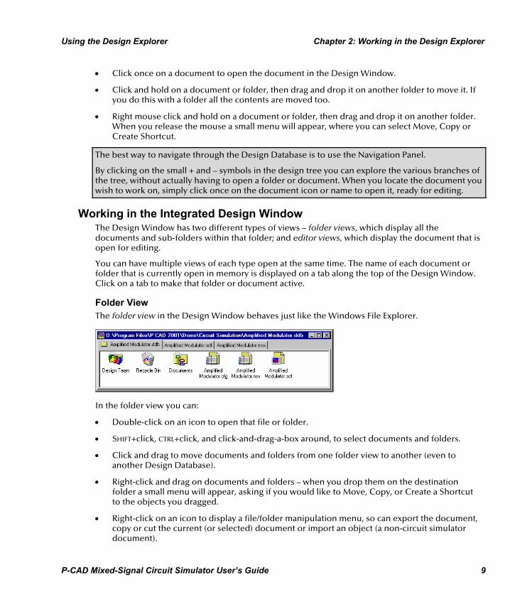
Folder View The folder view in the Design Window behaves just like the Windows File Explorer.
In the folder view you can:
• Double-click on an icon to open that file or folder.
• SHIFT+click, CTRL+click, and click-and-drag-a-box around, to select documents and folders.
• Click and drag to move documents and folders from one folder view to another (even to another Design Database).
• Right-click and drag on documents and folders – when you drop them on the destination folder a small menu will appear, asking if you would like to Move, Copy, or Create a Shortcut to the objects you dragged.
• Right-click on an icon to display a file/folder manipulation menu, so can export the document, copy or cut the current (or selected) document or import an object (a non-circuit simulator document).
Chapter 2: Working in the Design Explorer Using the Design Explorer
10 P-CAD Mixed-Signal Circuit Simulator User’s Guide
• Right-click elsewhere in the folder view to display a different menu, so you can create new documents or folders, import documents, link to external documents, paste from the clipboard or change the view.
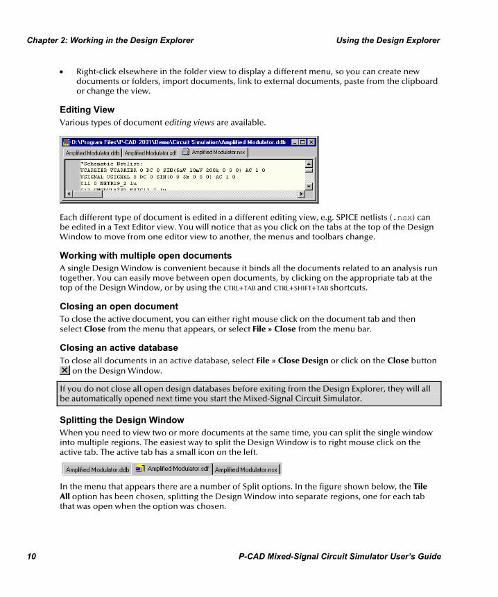
Editing View Various types of document editing views are available.
Each different type of document is edited in a different editing view, e.g. SPICE netlists (.nsx) can be edited in a Text Editor view. You will notice that as you click on the tabs at the top of the Design Window to move from one editor view to another, the menus and toolbars change.
Working with multiple open documents A single Design Window is convenient because it binds all the documents related to an analysis run together. You can easily move between open documents, by clicking on the appropriate tab at the top of the Design Window, or by using the CTRL+TAB and CTRL+SHIFT+TAB shortcuts.
Closing an open document To close the active document, you can either right mouse click on the document tab and then select Close from the menu that appears, or select File » Close from the menu bar.
Closing an active database To close all documents in an active database, select File » Close Design or click on the Close button
on the Design Window.
If you do not close all open design databases before exiting from the Design Explorer, they will all be automatically opened next time you start the Mixed-Signal Circuit Simulator.
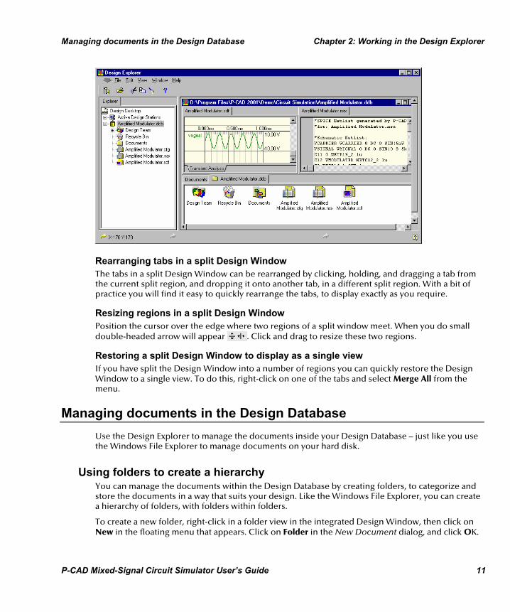
Splitting the Design Window When you need to view two or more documents at the same time, you can split the single window into multiple regions. The easiest way to split the Design Window is to right mouse click on the active tab. The active tab has a small icon on the left.
In the menu that appears there are a number of Split options. In the figure shown below, the Tile All option has been chosen, splitting the Design Window into separate regions, one for each tab that was open when the option was chosen.
Managing documents in the Design Database Chapter 2: Working in the Design Explorer
P-CAD Mixed-Signal Circuit Simulator User’s Guide 11
Rearranging tabs in a split Design Window The tabs in a split Design Window can be rearranged by clicking, holding, and dragging a tab from the current split region, and dropping it onto another tab, in a different split region. With a bit of practice you will find it easy to quickly rearrange the tabs, to display exactly as you require.
Resizing regions in a split Design Window Position the cursor over the edge where two regions of a split window meet. When you do small double-headed arrow will appear . Click and drag to resize these two regions.
Restoring a split Design Window to display as a single view If you have split the Design Window into a number of regions you can quickly restore the Design Window to a single view. To do this, right-click on one of the tabs and select Merge All from the menu.
Managing documents in the Design Database Use the Design Explorer to manage the documents inside your Design Database – just like you use the Windows File Explorer to manage documents on your hard disk.
Using folders to create a hierarchy You can manage the documents within the Design Database by creating folders, to categorize and store the documents in a way that suits your design. Like the Windows File Explorer, you can create a hierarchy of folders, with folders within folders.
To create a new folder, right-click in a folder view in the integrated Design Window, then click on New in the floating menu that appears. Click on Folder in the New Document dialog, and click OK.

Chapter 2: Working in the Design Explorer Managing documents in the Design Database
12 P-CAD Mixed-Signal Circuit Simulator User’s Guide
The new folder will appear with a generic name, like Folder1. To rename the folder, click once on the folder to select it, then select Edit » Rename from the menus. The text will appear highlighted, ready to type in the new name.
Moving, copying and deleting documents The Design Explorer supports all the familiar File Explorer shortcuts:
• SHIFT+click, CTRL+click, and click and drag a window, to select documents and folders
• Press the DELETE key to delete the current selection
• Drag and drop from one folder into another folder, to move the current selection
• Right-click, drag and drop a selection to pop up a menu, where you can choose between Copy, Move and Create Shortcut
• Press CTRL+C to copy the current selection, then CTRL+V to paste
• Right-click on a selection to display a menu, you can Copy, Cut, Delete, etc.
Renaming a document or folder To rename a document or folder, first select it (click once on its icon), then select Edit » Rename from the menus. An editing box will appear around the name and the text will be selected. Type in the new name, including any file extension.

P-CAD Mixed-Signal Circuit Simulator User’s Guide 13
CHAPTER 3
Getting Started with Simulation
Creating the circuit To perform simulation analyses, all components/parts placed on your schematic must contain special simulation-specific information that tells the simulator how these components/parts are to be treated. These schematic components/parts must include a reference to an appropriate SPICE device model.
The simulation models can be found in \Design Explorer 99 SE\Library\Sim\ within the drive and directory where you installed your Design Explorer 99 SE software. The models are stored in folders relating to the manufacturer of the component. See Selecting simulation-ready components in the Components and Models chapter for more information.
Once you have created the circuit from the simulation-ready libraries, there are three simple steps to perform to be able to run a simulation:
1. Add the appropriate sources to power and excite the circuit
2. Define the points that you wish to observe
3. Setup the analyses.
You are then ready to run the simulation. Before you start simulating your own circuits, you might like to explore some of the example circuits. The Circuit Simulator includes a large number of example circuits that demonstrate the various analysis types, as well as showing how the various types of devices can be used.
Check out the example designs in the folder \P-CAD 2002\Demo\Circuit Simulation.
Refer to these examples as you explore the various Setup options for the simulator. As you experiment with the examples refer to the chapter, Setting Up and Running a Simulation, for information about how to configure each type of analysis.
Chapter 3: Getting Started with Simulation Adding the Source Components
14 P-CAD Mixed-Signal Circuit Simulator User’s Guide
Adding the Source Components Before you can run a simulation, you will need to add the appropriate source components to your schematic to power and excite the circuit. You can place them directly from the Simulation Sources library ( \P-CAD 2002\Lib\Simulation Source.lib).
The simulator includes DC, Sin, Pulse, Exponential, Piece Wise Linear, FM, F/V Converter and VCO source components, as well as linear and non-linear dependent source components.
Once the source is placed, double-click on it to set the values. Refer to the chapter Voltage and Current Sources for information on configuring source components.
Defining the points to be plotted The points in the circuit that will have their waveforms displayed are specified in the Analyses Setup dialog (select Simulate » Setup). At the bottom of the General tab there are two lists: Available Signals and Active Signals. A waveform will be automatically displayed for each variable in the Active Signals list. It does not matter if you do not include a variable now though; you can add and remove variables in the waveform display after the waveforms appear.
Refer to the topics on Specifying the Simulation Data that you want collected, displayed and stored in the Setting up and Running a Simulation chapter for more information about defining what is displayed.
Setting up the Analyses Select Simulate » Setup to pop up the Analyses Setup dialog, where all the simulation setup is performed. The dialog will open with the General tab displayed. Use this tab to enable each analysis that you wish to perform. Each of the remaining tabs in the dialog is used to configure that type of analysis. Refer to the chapter Setting up and Running a Simulation for details on setting up each type of analysis.
The Advanced button at the bottom of the Analyses Setup dialog gives you access to a number of SPICE variables. These are advanced settings, generally you will only need to change these if the circuit is difficult to simulate, or you have a specific reason to change them. Refer to the chapter SPICE Variables and Analog Options for more information on each variable. If you are having difficulties getting the circuit to simulate, refer to Troubleshooting Simulation Problems.
Running a simulation Once the analyses have been configured you are ready to run a simulation. This can be done by pressing the Run Analyses button in the Analyses Setup dialog, or by selecting Simulate » Run from the menus. The simulation progress is displayed on the status bar. If an error is detected during netlisting, the simulation is stopped and a message box appears, asking if you would like to view the error file. Review this file and correct any errors. For more information, refer to the chapter Troubleshooting Simulation Problems.

Viewing the simulation results Chapter 3: Getting Started with Simulation
P-CAD Mixed-Signal Circuit Simulator User’s Guide 15
Viewing the simulation results Once the simulation is complete the results are automatically displayed in a separate waveform analysis window. Click on the tabs at the bottom of this window to display the results of each type of analysis. You can adjust your view of the waveforms with the Scaling controls on the Browse SimData panel. If this panel is not displayed, select View » Design Manager to show the Explorer and Browse SimData panels. Click on the SimData tab to display the panel.
Refer to chapter The Waveform Analysis Window for information on using the Scaling controls and the measurement cursors.

P-CAD Mixed-Signal Circuit Simulator User’s Guide 17
CHAPTER 4
Setting up and Running a Simulation
This chapter covers how to set up the options for different types of analyses and then how to run the simulation.
Before you can successfully simulate your circuit, you need to ensure that your schematic documents contain all the necessary information. In general, the following rules must be adhered to before you will be able to run any of the available simulations:
• All components and parts in the schematic must properly reference a simulation device model.
• You must place and wire up suitable signal sources to provide drive to the circuit during simulations.
• You must add meaningful net names to identify nodes in the circuit for which you wish to plot simulation data.
• If necessary, you must set the initial simulation conditions of the circuit.
Setting up a simulation run Before performing a simulation run, you need to select which analyses will be performed, the signals for which data will be collected and which variable waveforms will be automatically displayed when the simulation has finished.
The simulation options are set from either the P-CAD Schematic Editor or the Mixed-Signal Circuit Simulator, by selecting Simulate » Setup from the menus to open the Analyses Setup dialog.
The options that appear in this dialog are saved in a simulation configuration file (DesignName.cfg) which is stored in the design database. Each time you make a change to the simulation configuration, the settings are saved in this file. The simulation file is linked to the schematic of the same name, therefore each time you run a simulation, the correct settings for the particular circuit are used.

Chapter 4: Setting up and Running a Simulation Running a simulation from the Schematic design
18 P-CAD Mixed-Signal Circuit Simulator User’s Guide
Running a simulation from the Schematic design To run a simulation from the P-CAD Schematic design, select Simulate » Run or Simulate » Setup from the P-CAD Schematic main menus. The SPICE netlist is created and automatically imported into a design database with the same name as the schematic design, in the Design Explorer 99 SE environment. The netlist is then automatically opened and displayed.
If the Simulate » Run command was chosen, the simulation will be automatically performed by the Mixed-Signal Circuit Simulator. If the Simulate » Setup command was chosen, the Analyses Setup dialog will appear, from where you can configure all options and analyses for the simulator.
You can run the simulation directly from the Analyses Setup dialog by pressing the Run Analyses button within the dialog. Refer to each analysis topic later in this chapter for details on how to configure the simulator to perform that particular type of analysis.
When you run a simulation, the original netlist is combined with information from the configuration file (DesignName.cfg), to create the netlist that is actually used by the SPICE engine. The netlist that is generated from the schematic contains no setup information. The configuration file contains setup information only, which is obtained from the selections you make in the Analyses Setup dialog. A default .cfg file is created when a simulation is run for the first time. This combined netlist is a temporary file that is deleted after the simulation has completed.
You can also generate the SPICE netlist from the schematic using the Utils » Generate Netlist command. Make sure that you select XSpice as the format for your generated file. The simulation is not run automatically in this case and you will have to import the file into the design database in order to run the simulation using the Mixed-Signal Circuit Simulator. See the following section Running a simulation directly from the Mixed-Signal Circuit Simulator for more information.

Running a simulation directly from the Circuit Simulator Chapter 4: Setting up and Running a Simulation
P-CAD Mixed-Signal Circuit Simulator User’s Guide 19
The Status bar displays the progress whenever a simulation is running. As the simulation runs, a simulation waveform tab will open automatically to display the results of the analyses. Once the simulation is complete, the results will be displayed in the Simulation analysis window. This window includes a tab at the bottom for each type of analysis that has been performed. Refer to The Waveform Analysis Window, for more information on working with the waveforms.
The Status bar shows the progress, and the waveform window displays the results.
If an error is encountered during a simulation run, an error file (DesignName.err) will be created and displayed.
Running a simulation directly from the Circuit Simulator There may be instances when you wish to run the simulation directly from the SPICE netlist within the Mixed-Signal Circuit Simulator, without having to go back into P-CAD Schematic and running the simulation.
If you have previously run a simulation from the schematic, the SPICE netlist will automatically be imported and opened in the Mixed-Signal Circuit Simulator. If you have generated the netlist from the schematic using the Utils » Generate Netlist command and selecting the XSpice format, you will need to import the .nsx file into the design database. Once the file has been imported into the database, it can be opened and used by the Mixed-Signal Circuit Simulator.
With the SPICE netlist as the active document, you can run a simulation directly by selecting Simulate » Run from the menus. If you want to change any setup information, select Simulate » Setup from the menus. The Analyses Setup dialog will appear, from where you can make changes
Chapter 4: Setting up and Running a Simulation Specifying the simulation data
20 P-CAD Mixed-Signal Circuit Simulator User’s Guide
to your analyses criteria. You can run the simulation directly from the Analyses Setup dialog by pressing the Run Analyses button within the dialog.
As the simulation runs, a simulation waveform tab will open automatically to display the results of the analyses. If an error is encountered during a simulation run, an error file (DesignName.err) will be created and displayed.
Specifying the simulation data This section covers specifying the simulation data that you want collected, displayed and stored.
The General tab of the Setup Analyses dialog includes options that specify what type of analysis data is saved in the result file and what waveforms will be automatically displayed in the waveform window.
Specifying simulation data to be collected Since an enormous amount of data can be collected during a simulation, you can specify which points on the circuit and what type of data you wish to save as simulation results.
To specify the data to be collected and saved, from the P-CAD Schematic Editor or the Mixed-Signal Circuit Simulator, select Simulate » Setup from the menus and click on the General tab in the Analyses Setup dialog.
The Collect Data For option specifies exactly what kind of information you want to be calculated and stored in the result file. Select the required option from the drop down list. The list has five options. Select one of the first four options to specify exactly what information you want the simulator to calculate (voltages, currents, power, impedances, etc) and store in the results file.

Specifying the simulation data Chapter 4: Setting up and Running a Simulation
P-CAD Mixed-Signal Circuit Simulator User’s Guide 21
For each of the first four options, the data is stored for all available signals in the circuit. The fifth option, Active Signals, instructs the simulator to only store data for the signals that you have added to the Active Signals list below. The five options available are:
Node Voltage and Supply Current: Saves data for the voltage at each node and the current in each supply.
Node Voltage, Supply and Device Current: Saves data for the voltage at each node, and the current in each supply and each device.
Node Voltage, Supply Current, Device Current and Power: Saves data for the voltage at each node, the current in each supply, and the current and power in each device.
Node Voltage, Supply Current and Subcircuit VARs: Saves data for the voltage at each node, the current sourced from each supply and the voltages/currents calculated in subcircuit signals.
Active Signals: Saves results ONLY for signals shown in the Active Signals list. Use this option when you want to minimize the size of the result file. Signals are restricted to node voltages and supply currents. The Active Signals option is also used to limit which nodes are examined during the multi-pass simulations (Monte Carlo, Parameter Sweep and Temperature Sweep). If the Active Signals option is not chosen, data is collected for all nodes in the circuit for these analyses.
Specifying simulation data to be displayed When setting up a simulation, you can choose which signals are automatically displayed by the simulation viewer after the analyses have been done.
The Available Signals field shows a list of all available circuit signals that can be plotted. Which signals are available is determined by the type of data that is being collected and saved in the result document, set by the Collect Data For option.
To have a variable automatically plotted in the simulation viewer, select the variable in the Available Signals list and click the Include button to move the variable into the Active Signals list. Each variable that you include in the Active Signals list will be automatically displayed in the result waveform window. To remove a variable from the Active Signals list, select it and click the button. To include all variables in the Active Signals list, use the button and use to remove all.
Double-clicking on a variable also moves it from one list to the other. You can select multiple signals in a list by clicking-and-dragging the mouse over the variable list, or using the SHIFT and CTRL keys while clicking on signals.
While including a variable in the Active Signals list causes the simulation results for that variable to be automatically displayed in the waveform viewer, once the simulation has finished, you can use the controls in the waveform viewer to display any variable for which data was collected.
SimView Setup When you run a simulation, the results are displayed in the SimView Waveform Window. In the Waveform Window you can rearrange the display to suit your needs; you can change the scaling, add different nodes, remove existing nodes, and so on. When you close the Simulation Data File (.SDF), the setup information is saved with the file.

Chapter 4: Setting up and Running a Simulation Selecting Analyses to run
22 P-CAD Mixed-Signal Circuit Simulator User’s Guide
If you have previously run an simulation, the settings used for that simulation run are stored in your design. By default, the simulation uses the simulation viewer information from the previous simulation run to display the simulation results. If you change the Active Signals list from a previous simulation run, you must set the SimView Setup option in the General tab of the Analyses Setup dialog to Show Active Signals, for any changes to the displayed waveforms to take effect. When this option is on, the simulation viewer is reset to its default condition and the plot waveforms are read from the dialog list, rather than from the previous simulation run.
Selecting Analyses to run All simulation parameters can be set from either the P-CAD Schematic Editor or the Mixed-Signal Circuit Simulator, by selecting Simulate » Setup from the menus to open the Analyses Setup dialog. This dialog controls all of the available simulation analyses and allows you to select which analyses will be performed.
Transient Analysis A Transient analysis generates output like that normally shown on an oscilloscope, computing the transient output variables (voltage or current) as a function of time, over the user-specified time interval. An Operating Point analysis is automatically performed prior to a Transient analysis to determine the DC bias of the circuit, unless the Use Initial Conditions option is enabled. Refer to the topic When to Use the Initial Conditions Option later in this section for more information on this option.
A Transient analysis calculates the voltages and currents as a function of time
Selecting Analyses to run Chapter 4: Setting up and Running a Simulation
P-CAD Mixed-Signal Circuit Simulator User’s Guide 23
Setting up for a Transient Analysis A Transient analysis always begins at time zero. In the time interval between zero and Start Time, the simulator analyzes the circuit but does not store the results. In the time interval between Start Time and Stop Time it continues to analyze the circuit, storing the results ready for display on completion of the analysis.
Step Time is the nominal time increment used in the analysis, however the actual timestep is varied automatically by the simulator in order to achieve convergence. The Maximum Step limits the varying size of the timestep that the simulator can use when calculating the transient data; by default it chooses either Step Time or (Stop Time - Start Time)/50, whichever is smaller. Typically Step Time and Maximum Step are set to the same value.
Automatically calculating the Transient Analysis Parameters If you are not sure what values to enter, press the Set Defaults button to automatically calculate the Transient analysis parameters. Start Time is set to zero and Stop Time, Step Time and Maximum Step are calculated using the Defaults; Cycles Displayed and Points per Cycle, based on the lowest frequency Source in the circuit. For example, if the lowest frequency source in the circuit was 10KHz and the Defaults were Cycles Displayed = 5 and Points per Cycle = 50 then:
Stop Time = 1/10KHz * 5 = 100uS * 5 = 500uS
Step Time = (1/10000) / 50 = 2uS
Max Step = Step Time = 2uS
If the Always set defaults option is enabled for a transient analysis, the simulator acts as if this button is pressed before each simulation.
When to Use the Initial Conditions Option If you enable the Use Initial Conditions option, the Transient analysis begins from the defined initial conditions, bypassing the Operating Point analysis. Use this option when you wish to perform a transient analysis starting from other than the quiescent operating point.
Chapter 4: Setting up and Running a Simulation Selecting Analyses to run
24 P-CAD Mixed-Signal Circuit Simulator User’s Guide
To use this option you must either define the initial condition for each appropriate component in the circuit, or place .IC devices on the circuit. An initial value of zero is assumed for a component that does not have the Initial Condition defined.
The IC value of a component overrides a .IC object attached to a net.
Running a Transient Analysis To run a Transient analysis:
1. Set up the Transient analysis parameters as described above.
2. Enable the Transient/Fourier Analysis option in the General tab of the Analyses Setup dialog (select Simulate » Setup).
3. After enabling this option, you press the Run Analyses button at the bottom of the dialog, or select the Simulate » Run menu item to start the simulation process.
The simulation progress is displayed on the status bar. If an error is detected during netlisting, the simulation is stopped and a message box appears, asking if you would like to view the error file. Review this file and correct any errors. For more information, refer to the chapter Troubleshooting Simulation Problems.
Once the design is netlisted, the waveform window will appear, displaying the simulation results as they are calculated.
You can then view and measure voltage, current and power dissipation waveforms of the circuit in the analysis window that is displayed. Refer to the chapter, The Waveform Analysis Window, for more information on working in this window.
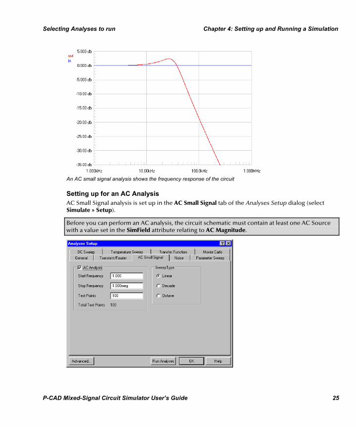
AC Small Signal Analysis (AC Sweep) AC analysis generates output that shows the frequency response of the circuit, calculating the small signal AC output variables as a function of frequency. It first performs an Operating Point analysis to determine the DC bias of the circuit, replaces the signal source with a fixed amplitude sine wave generator, then analyzes the circuit over the specified frequency range. The desired output of an AC small signal analysis is usually a transfer function (voltage gain, transimpedance, etc.).
Selecting Analyses to run Chapter 4: Setting up and Running a Simulation
P-CAD Mixed-Signal Circuit Simulator User’s Guide 25
An AC small signal analysis shows the frequency response of the circuit
Setting up for an AC Analysis AC Small Signal analysis is set up in the AC Small Signal tab of the Analyses Setup dialog (select Simulate » Setup).
Before you can perform an AC analysis, the circuit schematic must contain at least one AC Source with a value set in the SimField attribute relating to AC Magnitude.
Chapter 4: Setting up and Running a Simulation Selecting Analyses to run
26 P-CAD Mixed-Signal Circuit Simulator User’s Guide
At least one Source in the circuit must include a value in the SimField attribute relating to AC Magnitude. This Source is replaced with a sine wave generator during simulation which has its frequency swept from Start Frequency to Stop Frequency, stepping in increments defined by Test Points and the Sweep Type.
Set the Sweep Type to define how the test points are determined. The Sweep options are defined below:
Sweep Type What it Means
Linear Total number of Test Points in the sweep
Decade Number of Test Points per decade in the sweep
Octave Number of Test Points per octave in the sweep
The amplitude and phase of the swept sine wave are specified in the relevant SimField attributes of the Source in the schematic. Double click on the source to set these values. Enter the amplitude in the SimField attribute relating to AC Magnitude (in volts) and the phase in the SimField attribute relating to AC Phase (in degrees). Units are not required. Set the AC amplitude to 1 to have the output signals displayed relative to 0 dB.
Running an AC Small Signal Analysis To run an AC Small Signal analysis:
1. Set up the AC Small Signal analysis parameters as described above.
2. Ensure that there is at least one Source in the circuit with a value in the SimField attribute relating to AC Magnitude (in volts).
3. Enable the AC Small Signal Analysis option in the General tab of the Analyses Setup dialog (select Simulate » Setup).
4. After enabling this option you can either press the Run Analyses button at the bottom of the dialog, or select the Simulate » Run menu item to start the simulation process.
The simulation progress is displayed on the status bar. If an error is detected during netlisting the simulation is stopped and a message box appears, asking if you would like to view the error file. Review this file and correct any errors. For more information, refer to the chapter Troubleshooting Simulation Problems.
Once the design is netlisted the waveform window will appear, displaying the simulation results as they are calculated. You can then view and measure voltage, current and power dissipation waveforms of the circuit in the analysis window that is displayed. Refer to the chapter, The Waveform Analysis Window, for more information on working in this window.
DC Sweep Analysis The DC Sweep analysis generates output like that of a curve tracer. It performs a series of Operating Point analyses, modifying the voltage of a selected source in pre-defined steps, to give a DC transfer curve. You can also specify an optional secondary source. If a secondary source is

Selecting Analyses to run Chapter 4: Setting up and Running a Simulation
P-CAD Mixed-Signal Circuit Simulator User’s Guide 27
specified the primary source is stepped over its entire range for each value of the secondary source.
A DC Transfer analysis – each curve shows the output voltage, as the input voltage (primary source) is stepped from –0.7V to –1.5V. The supply voltage (secondary source) is stepped to give the set of curves.
Setting up for a DC Sweep Analysis DC Sweep analysis is set up in the DC Sweep tab of the Analyses Setup dialog (select Simulate » Setup).

Chapter 4: Setting up and Running a Simulation Selecting Analyses to run
28 P-CAD Mixed-Signal Circuit Simulator User’s Guide
Source Name is the name of the independent power source in the circuit that is to be stepped. The start, stop and step values define the sweep range and resolution. The primary source is required, and the secondary source is optional.
Running a DC Sweep Analysis 1. Set up the DC Sweep analysis parameters as described above.
2. Enable the DC Sweep Analysis option in the General tab of the Analyses Setup dialog (select Simulate » Setup).
3. After enabling this option, you can either press the Run Analyses button at the bottom of the dialog, or select the Simulate » Run menu item to start the simulation process.
The simulation progress is displayed on the status bar. If an error is detected during netlisting the simulation is stopped and a message box appears, asking if you would like to view the error file. Review this file and correct any errors. For more information, refer to the chapter Troubleshooting Simulation Problems.
Once the design is netlisted the waveform window will appear, displaying the simulation results as they are calculated.
You can then view and measure the transfer curves from the waveforms in the analysis window that is displayed. Refer to the chapter, The Waveform Analysis Window, for more information on working in this window.
DC Operating Point Analysis Prior to performing a Transient or an AC Small Signal analysis, the simulator must first perform an Operating Point analysis. The Operating Point analysis determines the DC bias of the entire circuit, with inductors considered to be short circuit and capacitors open circuit. It also determines linearized, small-signal models for all nonlinear devices in the circuit that are used in the AC Small Signal analysis. It does not take into account the existence of any AC sources.
Running an Operating Point Analysis The Operating Point analysis is performed automatically whenever a Transient or AC Small Signal analysis is enabled. These results are used internally by the simulation engine. If you want to examine the results of the operating point calculations you can enable the Operating Point analysis. To do this:
1. Enable the Operating Point Analysis in the General tab of the Analyses Setup dialog (select Simulate » Setup).
2. To include the current, power and impedance calculations set the Collect Data For option in the General tab of the Analyses Setup dialog to Node Voltage, Supply Current, Device Currents and Power.
3. After enabling this option you can either press the Run Analyses button at the bottom of the dialog, or select the Simulate » Run menu item to start the simulation process.
The simulation progress is displayed on the status bar. If an error is detected during netlisting the simulation is stopped and a message box appears, asking if you would like to view the error file.
Selecting Analyses to run Chapter 4: Setting up and Running a Simulation
P-CAD Mixed-Signal Circuit Simulator User’s Guide 29
Review this file and correct any errors. For more information, refer to the chapter Troubleshooting Simulation Problems.
You can then view the results in the Operating Point tab of the analysis window that is displayed. You can add nodes and devices to the list of results by selecting them in the Waveforms list in the Browse SimData panel and clicking the Show button.
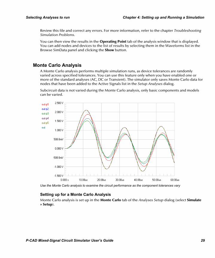
Monte Carlo Analysis A Monte Carlo analysis performs multiple simulation runs, as device tolerances are randomly varied across specified tolerances. You can use this feature only when you have enabled one or more of the standard analyses (AC, DC or Transient). The simulator only saves Monte Carlo data for nodes that have been added to the Active Signals list in the Setup Analyses dialog.
Subcircuit data is not varied during the Monte Carlo analysis, only basic components and models can be varied.
Use the Monte Carlo analysis to examine the circuit performance as the component tolerances vary
Setting up for a Monte Carlo Analysis Monte Carlo analysis is set up in the Monte Carlo tab of the Analyses Setup dialog (select Simulate » Setup).

Chapter 4: Setting up and Running a Simulation Selecting Analyses to run
30 P-CAD Mixed-Signal Circuit Simulator User’s Guide
The Monte Carlo options are set up as follows:
Simulation Runs Enter the number of simulation runs you want the simulator to perform. For example, if you enter 10, then ten simulation runs will be performed, with different device values on each run, within the specified tolerance range.
Simulation Seed The simulator uses the seed to generate random numbers for the Monte Carlo runs. The default seed value is –1. If you want to run a simulation with a different series of random numbers you must change the seed value to another number.
Default Distribution You can choose from the following three distributions for random number generation in the Monte Carlo analysis:
Uniform distribution
Uniform distribution is a flat distribution. Values are uniformly distributed over the specified tolerance range. For example, for a 1K resistor with a tolerance of 10 percent there is an equal chance of the generated value being anywhere between 900 ohms and 1100 ohms.
Gaussian distribution
Values are distributed according to a Gaussian (bell-shaped) curve, with the center at the nominal value and the specified tolerance at +/- 3 standard deviations. For a resistor with a value of 1K +/-10% the center of the distribution would be at 1000 ohms, + 3 standard deviations is 1100 ohms, and
Selecting Analyses to run Chapter 4: Setting up and Running a Simulation
P-CAD Mixed-Signal Circuit Simulator User’s Guide 31
–3 standard deviations is 990 ohms. With this type of distribution there is a higher probability that the generated value will be closer to the specified value.
Worst Case distribution
This is the same as the uniform distribution, but only the end points (worst case) of the range are used. For a 1K +/-10% resistor the value used would be randomly chosen from the two worst case values of 990 ohms and 1100 ohms. On any one simulation run there is an equal chance that the high-end worst case value (1100) or low-end worst case value (990) will be used.
Specifying Default Tolerances You can specify default tolerances for six general categories of devices: resistor, capacitor, inductor, DC source, transistor (beta forward), and digital Tp (propagation delay for digital devices).
Tolerances can be specified as actual values, or as percentages. For example, you can enter a resistor tolerance as 10 or 10%. If a 1kohm resistor has a tolerance of 10, it varies between 990 and 1010 ohms. With a tolerance of 10%, a 1kohm resistor varies between 900 and 1100 ohms.
Each device is randomly varied independent of other devices. For example, if a circuit has two 10kohm resistors, and the default tolerance is set to 10%, then during the first pass of the simulation, one resistor might have a value of 953 ohms, and the other one could be 1022 ohms. The simulator uses a separate and independent random number to generate the value for each device.
Specific Device Tolerances You can also override Default Tolerances with specific device tolerances. To add a Specific Device Tolerance, right-click in the Specific Device Tolerance region of the dialog and select Add from the pop-up menu that appears (shortcut: press the Insert key). The Monte Carlo Device and Lot Tolerances dialog will pop up. The attributes of this dialog are:
Designator
Select the required circuit device.
Parameter
Include a parameter if the device requires it. Supported parameters include the propagation delay of a digital component, the Beta forward of a transistor, and the resistance of a potentiometer.
Device Tolerance
Tolerance of this device.
Device Tracking Number
Assign a common tracking number to devices when you require the variation in their tolerance to be correlated. If you give two devices the same Device Tracking Number and Device Distribution then the same random number is used for both devices when the device values for a simulation run are calculated.

Chapter 4: Setting up and Running a Simulation Selecting Analyses to run
32 P-CAD Mixed-Signal Circuit Simulator User’s Guide
Device Distribution
Select the distribution kind for this device, as described earlier in this topic.
Lot Tolerance, Tracking and Distribution
These settings are used in exactly the same way as the Device settings. They provide a second way of defining and correlating device tolerances. Both device and lot tolerances are allowed, but only one or the other is required. The simulator calculates device and lot tolerances independently (using different random numbers) and then adds them together.
Combined device and lot tolerances are useful where values are not completely correlated, but are not completely independent either. An example would be two different resistor packs. Here, the lot tolerance can be large (that is, the variation from wafer to wafer), while the device tolerance (the variation from resistor to resistor in the same package), is small. In this case the device tolerance should not be ignored because it may limit the overall performance of a circuit.
Consider the following example:
Assume R1 and R2 are both 1k, with a Device Tolerance of 1% (no device tracking) and they have a Lot Tolerance of 4%, with the same Lot Tracking number. For each Monte Carlo run the resistors are first assigned the same lot variation (a nominal value) between +/- 4%. Then each resistor is assigned a device tolerance between +/- 1%. This gives a total tolerance of 5% (1% + 4%). However, during the same run the values of each resistor cannot be any farther than +/- 1% from their nominal value, or 2% from each other.
Running a Monte Carlo Analysis To run a Monte Carlo analysis:
1. Set up the Monte Carlo analysis parameters as described above.
2. Enable the Monte Carlo Analysis option in the General tab of the Analyses Setup dialog (select Simulate » Setup).
3. Monte Carlo analysis can result in a large amount of data being calculated. To limit the amount of data that is calculated, you can set the Collect Data For option in the Analyses Setup dialog to Active Signals. With this option, Monte Carlo data is only calculated for the variables currently listed in the Active Signals field.
4. After enabling this option you can either press the Run Analyses button at the bottom of the dialog, or select the Simulate » Run menu item to start the simulation process.
The simulation progress is displayed on the status bar. If an error is detected during netlisting the simulation is stopped and a message box appears, asking if you would like to view the error file. Review this file and correct any errors. For more information, refer to the chapter Troubleshooting Simulation Problems.
Once the design is netlisted the waveform window will appear, displaying the simulation results as they are calculated. The simulator displays the results of the Monte Carlo analysis in the AC, DC or Transient analysis window(s), depending on which analyses were enabled. You can then view and measure the Monte Carlo analysis results from the waveforms in the analysis window. Refer to the chapter, The Waveform Analysis Window, for more information on working in this window.

Selecting Analyses to run Chapter 4: Setting up and Running a Simulation
P-CAD Mixed-Signal Circuit Simulator User’s Guide 33
Parameter Sweep The Parameter Sweep feature allows you to sweep the value of a device in defined increments, over a specified range. The simulator performs multiple passes of the enabled analyses (AC, DC or Transient). The Parameter Sweep can vary basic components and models, note that subcircuit data is not varied during the analysis.
You can also define a Secondary parameter to be swept. When a Secondary parameter is defined, the Primary parameter is swept for each value of the Secondary parameter. For example, if the step sizes are set so that there will be three passes of the Primary sweep and three passes of the Secondary sweep, the component values will be P1 and S1, P2 and S1, P3 and S1, then P1 and S2, P2 and S2, P3 and S2, and so on.
The voltage at the node OUT, as one of the component values in the circuit is swept
Setting up for a Parameter Sweep A Parameter Sweep is set up in the Parameter Sweep tab of the Analyses Setup dialog (select Simulate » Setup).
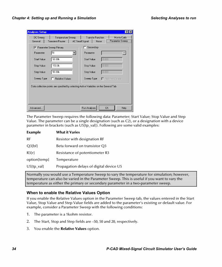
Chapter 4: Setting up and Running a Simulation Selecting Analyses to run
34 P-CAD Mixed-Signal Circuit Simulator User’s Guide
The Parameter Sweep requires the following data: Parameter; Start Value; Stop Value and Step Value. The parameter can be a single designation (such as C2), or a designation with a device parameter in brackets (such as U5[tp_val]). Following are some valid examples:
Example What it Varies
RF Resistor with designation RF
Q3[bf] Beta forward on transistor Q3
R3[r] Resistance of potentiometer R3
option[temp] Temperature
U5[tp_val] Propagation delays of digital device U5
Normally you would use a Temperature Sweep to vary the temperature for simulation; however, temperature can also be varied in the Parameter Sweep. This is useful if you want to vary the temperature as either the primary or secondary parameter in a two-parameter sweep.
When to enable the Relative Values Option If you enable the Relative Values option in the Parameter Sweep tab, the values entered in the Start Value, Stop Value and Step Value fields are added to the parameter’s existing or default value. For example, consider a Parameter Sweep with the following conditions:
1. The parameter is a 1kohm resistor.
2. The Start, Stop and Step fields are –50, 50 and 20, respectively.
3. You enable the Relative Values option.

Selecting Analyses to run Chapter 4: Setting up and Running a Simulation
P-CAD Mixed-Signal Circuit Simulator User’s Guide 35
The following resistor values would be used in the simulation runs: 950, 970, 990, 1010, 1030 and 1050.
Running a Parameter Sweep To perform a Parameter Sweep:
1. Parameter Sweep analysis can result in a large amount of data being calculated. To limit the amount of data that is calculated, you can set the Collect Data For option in the Analyses Setup dialog to Active Signals. With this option data is only calculated for the variables currently listed in the Active Signals field.
2. Set up the Parameter Sweep parameters as described above.
3. Enable the Parameter Sweep option in the General tab of the Analyses Setup dialog (select Simulate » Setup).
4. After enabling this option you can either press the Run Analyses button at the bottom of the dialog, or select the Simulate » Run menu item to start the simulation process.
The simulation progress is displayed on the status bar. If an error is detected during netlisting the simulation is stopped and a message box appears, asking if you would like to view the error file. Review this file and correct any errors. For more information, refer to the chapter Troubleshooting Simulation Problems.
Once the design is netlisted the waveform window will appear, displaying the simulation results as they are calculated. The simulator displays the results of the Parameter Sweep in the AC, DC or Transient analysis window(s), depending on which analyses were enabled. You can then view and measure the Parameter Sweep results from the waveforms in the analysis window. Refer to the chapter, The Waveform Analysis Window, for more information on working in this window.
Temperature Sweep A Temperature Sweep can be used in conjunction with one or more of the standard analyses: AC; DC or Transient. The circuit is analyzed at each temperature in the specified range, producing a series of curves, one for each temperature setting.
Setting up a Temperature Sweep Analysis A Temperature Sweep is set up in the Temperature Sweep tab of the Analyses Setup dialog (select Simulate » Setup).
Set up one or more standard analysis so that each analysis is performed at the indicated temperatures. The Start Value and Stop Value define the range of temperatures for the sweep, and the Step Value defines step increment. The Temperature Sweep is only calculated for nodes defined in the Active Signals list.
Running a Temperature Sweep Analysis To run a Temperature Sweep analysis:
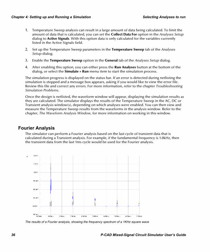
Chapter 4: Setting up and Running a Simulation Selecting Analyses to run
36 P-CAD Mixed-Signal Circuit Simulator User’s Guide
1. Temperature Sweep analysis can result in a large amount of data being calculated. To limit the amount of data that is calculated, you can set the Collect Data For option in the Analyses Setup dialog to Active Signals. With this option data is only calculated for the variables currently listed in the Active Signals field.
2. Set up the Temperature Sweep parameters in the Temperature Sweep tab of the Analyses Setup dialog.
3. Enable the Temperature Sweep option in the General tab of the Analyses Setup dialog.
4. After enabling this option, you can either press the Run Analyses button at the bottom of the dialog, or select the Simulate » Run menu item to start the simulation process.
The simulation progress is displayed on the status bar. If an error is detected during netlisting the simulation is stopped and a message box appears, asking if you would like to view the error file. Review this file and correct any errors. For more information, refer to the chapter Troubleshooting Simulation Problems.
Once the design is netlisted, the waveform window will appear, displaying the simulation results as they are calculated. The simulator displays the results of the Temperature Sweep in the AC, DC or Transient analysis window(s), depending on which analyses were enabled. You can then view and measure the Temperature Sweep results from the waveforms in the analysis window. Refer to the chapter, The Waveform Analysis Window, for more information on working in this window.
Fourier Analysis The simulator can perform a Fourier analysis based on the last cycle of transient data that is calculated during a Transient analysis. For example, if the fundamental frequency is 1.0kHz, then the transient data from the last 1ms cycle would be used for the Fourier analysis.
The results of a Fourier analysis, showing the frequency spectrum of a 1KHz square wave
Selecting Analyses to run Chapter 4: Setting up and Running a Simulation
P-CAD Mixed-Signal Circuit Simulator User’s Guide 37
Setting up a Fourier Analysis Fourier analysis is set up in the Transient/Fourier tab of the Analyses Setup dialog (select Simulate » Setup). You must enable the Transient analysis in order to do the Fourier analysis. Enter the Fundamental Frequency of the analysis, and the number of Harmonics required.
Running a Fourier Analysis To run a Fourier analysis:
1. Set up the Fourier analysis parameters as described above.
2. Enable the Transient/Fourier Analysis option in the General tab of the Analyses Setup dialog (select Simulate » Setup).
3. After enabling this option, you can either press the Run Analyses button at the bottom of the dialog, or select the Simulate » Run menu item to start the simulation process.
4. In the Fund. Frequency field, enter the fundamental frequency for the analysis. Enter the number of harmonics required in the Harmonics field.
The simulation progress is displayed on the status bar. If an error is detected during netlisting the simulation is stopped and a message box appears, asking if you would like to view the error file. Review this file and correct any errors. For more information, refer to the chapter Troubleshooting Simulation Problems.
Once the design is netlisted the waveform window will appear, displaying the simulation results as they are calculated.
Refer to the simulation information file (DesignName.SIM) for details of the magnitude and phase of each harmonic.
You can then view and measure the Fourier analysis waveforms in the analysis window that is displayed. Refer to the chapter, The Waveform Analysis Window, for more information on working in this window.
Transfer Function Analysis The Transfer Function analysis calculates the DC input resistance, DC output resistance and DC gain.
Setting up a Transfer Function Analysis Transfer Function analysis is set up in the Transfer Function tab of the Analyses Setup dialog (select Simulate » Setup). Select the Source to be used as the input reference for the calculations in the Source Name field. Select the node that the calculations are referenced to in the Reference Node field (the default is 0).
Running a Transfer Function Analysis To run a Transfer Function analysis:

Chapter 4: Setting up and Running a Simulation Selecting Analyses to run
38 P-CAD Mixed-Signal Circuit Simulator User’s Guide
1. Set up the Transfer Function analysis parameters as described above.
2. Enable the Transfer Function option in the General tab of the Analyses Setup dialog (select Simulate » Setup).
3. After enabling this option, you can either press the Run Analyses button at the bottom of the dialog, or select the Simulate » Run menu item to start the simulation process.
The simulation progress is displayed on the status bar. If an error is detected during netlisting, the simulation is stopped and a message box appears, asking if you would like to view the error file. Review this file and correct any errors. For more information, refer to the chapter Troubleshooting Simulation Problems.
Once the design is netlisted the waveform window will appear, displaying the simulation results as they are calculated.
You can then view the DC input resistance, DC output resistance and DC gain at each node in the circuit on the Transfer Function tab of the analysis window. Refer to the chapter The Waveform Analysis Window, for more information on working in this window.
Noise Analysis Noise analysis lets you measure the noise in your circuit due to noise contributions of resistors and semiconductor devices. The simulator can plot the Noise Spectral Density, which is the noise measured in Volts squared per Hertz (V^2/Hz). Capacitors, inductors and controlled sources are treated as noise free. The following noise measurements can be made in the simulator:
Output Noise The noise measured at a specified output node.
Input Noise The input noise is the amount of noise that, if injected at the input, would cause the calculated noise at the output. For example, if the output noise is 10p, and the circuit has a gain of 10, then it would take 1p of noise at the input to measure 10p of noise at the output. Thus the equivalent input noise is 1p.
Component Noise The output noise contribution of each component in the circuit. The total output noise is the sum of individual noise contributions of resistors and semiconductor devices. Each of these components contributes a certain amount of noise, which is multiplied by the gain from that component’s position to the circuit’s output. Thus the same component can contribute different amounts of noise to the output, depending on its location in the circuit.
Setting up a Noise Analysis Noise analysis is set up in the Noise tab of the Analyses Setup dialog (select Simulate » Setup).
Select the Noise Source to be used as the input reference for the noise calculations. Enter the Start and Stop Frequencies and the number of Test Points that the calculations will be performed at. The
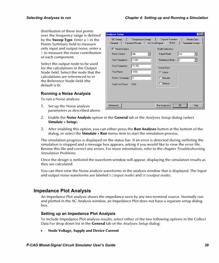
Selecting Analyses to run Chapter 4: Setting up and Running a Simulation
P-CAD Mixed-Signal Circuit Simulator User’s Guide 39
distribution of these test points over the frequency range is defined by the Sweep Type. Enter a 0 in the Points Summary field to measure only input and output noise, enter a 1 to measure the noise contribution of each component.
Select the output node to be used for the calculations in the Output Node field. Select the node that the calculations are referenced to in the Reference Node field (the default is 0).
Running a Noise Analysis To run a Noise analysis:
1. Set up the Noise analysis parameters as described above.
2. Enable the Noise Analysis option in the General tab of the Analyses Setup dialog (select Simulate » Setup).
3. After enabling this option, you can either press the Run Analyses button at the bottom of the dialog, or select the Simulate » Run menu item to start the simulation process.
The simulation progress is displayed on the status bar. If an error is detected during netlisting the simulation is stopped and a message box appears, asking if you would like to view the error file. Review this file and correct any errors. For more information, refer to the chapter Troubleshooting Simulation Problems.
Once the design is netlisted the waveform window will appear, displaying the simulation results as they are calculated.
You can then view the Noise analysis waveforms in the analysis window that is displayed. The Input and output noise waveforms are labeled NI(input node) and NO(output node).
Impedance Plot Analysis An Impedance Plot analysis shows the impedance seen by any two-terminal source. Normally run and plotted in the AC Analysis window, an Impedance Plot does not have a separate setup dialog box.
Setting up an Impedance Plot Analysis To include Impedance Plot analysis results, select either of the two following options in the Collect Data For drop down list in the General tab of the Analyses Setup dialog:
• Node Voltage, Supply and Device Current

Chapter 4: Setting up and Running a Simulation Mathematical Functions and Waveforms
40 P-CAD Mixed-Signal Circuit Simulator User’s Guide
• Node Voltage, Supply Current, Device Current and Power.
Locate the source of interest in the Available Signals list and add it to the Active Signals list. A source with a designator of VIN would appear in the list as @VIN(z). The z suffix indicates that the variable is an impedance plot.
Running an Impedance Plot Analysis When you run the simulation, an impedance plot will appear in the Analyses windows. This is especially useful to the impedance versus frequency in the AC Analysis window. The impedance measurement is calculated from the voltage at the supply’s positive terminal, divided by the current out of that same terminal.
You can also do an impedance plot of the circuit’s output impedance. To measure the circuit’s output impedance, the following steps must be followed, using your schematic design in the P-CAD Schematic Editor::
1. Remove the source from the input.
2. Ground the circuit’s inputs where the input supply was connected.
3. Remove any load connected to the circuit.
4. Connect a two-terminal source to the output, with the source’s positive terminal connected to the output and the source’s negative terminal connected to ground.
5. Setup the signals as described earlier.
6. Run the desired simulation.
For Impedance Plots, you would normally change the Y axis to Magnitude. To do this, the waveform display must be in single cell mode. Right-click in the waveform window and select Scaling from the pop up menu. Set the Y Axis to Magnitude in the Scaling Options dialog. Refer to Scaling the Waveforms’ Axes in the Waveform Analysis Window chapter for more information.
Mathematical Functions and Waveforms As part of the analysis of your design, you may want to perform a mathematical operation on one or more of the simulation signals, and view the resultant waveform. This feature is an integral part of the simulator’s waveform viewer. You can construct a mathematical expression based on any signal available in the simulated circuit.
To define a mathematical function, click the New button in the Browse SimData Panel, which pops up the Create New Waveform dialog. There are three parts to the dialog: a list of available Functions; a list of currently available Waveforms and an Expression building field. The Expression can be constructed by either typing it in directly, or by clicking to select a function in the Functions list, then clicking to select the signal that you want to apply that function to.
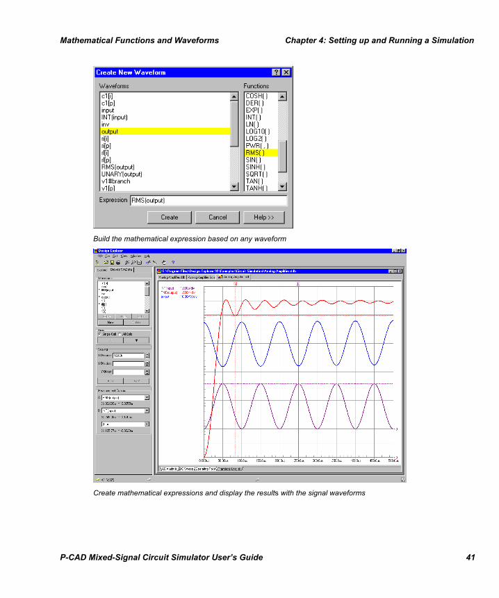
Mathematical Functions and Waveforms Chapter 4: Setting up and Running a Simulation
P-CAD Mixed-Signal Circuit Simulator User’s Guide 41
Build the mathematical expression based on any waveform
Create mathematical expressions and display the results with the signal waveforms
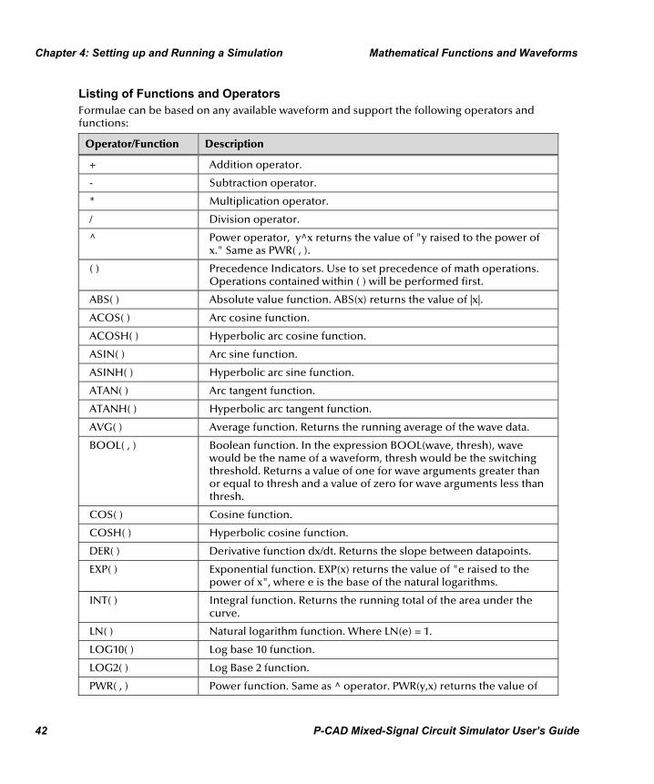
Chapter 4: Setting up and Running a Simulation Mathematical Functions and Waveforms
42 P-CAD Mixed-Signal Circuit Simulator User’s Guide
Listing of Functions and Operators Formulae can be based on any available waveform and support the following operators and functions:
Operator/Function Description
+ Addition operator.
- Subtraction operator.
* Multiplication operator.
/ Division operator.
^ Power operator, y^x returns the value of "y raised to the power of x." Same as PWR( , ).
( ) Precedence Indicators. Use to set precedence of math operations. Operations contained within ( ) will be performed first.
ABS( ) Absolute value function. ABS(x) returns the value of |x|.
ACOS( ) Arc cosine function.
ACOSH( ) Hyperbolic arc cosine function.
ASIN( ) Arc sine function.
ASINH( ) Hyperbolic arc sine function.
ATAN( ) Arc tangent function.
ATANH( ) Hyperbolic arc tangent function.
AVG( ) Average function. Returns the running average of the wave data.
BOOL( , ) Boolean function. In the expression BOOL(wave, thresh), wave would be the name of a waveform, thresh would be the switching threshold. Returns a value of one for wave arguments greater than or equal to thresh and a value of zero for wave arguments less than thresh.
COS( ) Cosine function.
COSH( ) Hyperbolic cosine function.
DER( ) Derivative function dx/dt. Returns the slope between datapoints.
EXP( ) Exponential function. EXP(x) returns the value of "e raised to the power of x", where e is the base of the natural logarithms.
INT( ) Integral function. Returns the running total of the area under the curve.
LN( ) Natural logarithm function. Where LN(e) = 1.
LOG10( ) Log base 10 function.
LOG2( ) Log Base 2 function.
PWR( , ) Power function. Same as ^ operator. PWR(y,x) returns the value of

Modifying the SPICE netlist for a simulation Chapter 4: Setting up and Running a Simulation
P-CAD Mixed-Signal Circuit Simulator User’s Guide 43
"y raised to the power of x."
RMS( ) Root-Mean-Square function. Returns the running AC RMS value of the wave data.
SIN( ) Sine function.
SINH( ) Hyperbolic sine function.
SQRT( ) Square root function.
TAN( ) Tangent function.
TANH( ) Hyperbolic tangent function.
UNARY( ) Unary minus function. UNARY(x) returns -x.
URAMP( ) Unit ramp function. Integral of the unit step: for an input x, the value is zero if x is less than zero, or if x is greater than zero, the value is x.
USTEP( ) Unit step function. Returns a value of one for arguments greater than zero and a value of zero for arguments less than zero.
Modifying the SPICE netlist for a simulation There are times when you may want to modify the netlist. If you don't want to go back to schematic to make a change, maybe to a value for a resistor or capacitor, you can edit the netlist directly from within the Mixed-Signal Circuit Simulator.
The netlist that is generated from the schematic design contains no setup information, with respect to analysis criteria. This is added from the configuration file to create a temporary netlist that is used by the SPICE engine at run time. The configuration file contains the setup information from the Analyses Setup dialog. If you want to add setup information directly into the netlist, use the Text Editor associated with the Mixed-Signal Circuit Simulator. If you generated your original netlist from the schematic design using Simulate » Run or Simulate » Setup, the netlist will have automatically opened in the Mixed-Signal Circuit Simulator and can be edited straight away. If you used Utils » Generate Netlist you will have to import the file into the design database and open it first, before you can edit.
Please Note: If you enter setup information into the netlist directly and then run the simulation from within the Mixed-Signal Circuit Simulator, a dialog will appear alerting you to the fact that setup information has been detected in the netlist. You are asked whether you want to run the simulation with the setup information that you entered manually or whether you want to use the setup information in the configuration file.
If you choose to run with the setup information you entered manually, the configuration file will not be used. If you choose to use the configuration file setup information, the criteria you entered manually will not be used. You cannot use setup information entered manually in conjunction with the information stored in the configuration file.
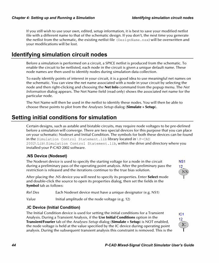
Chapter 4: Setting up and Running a Simulation Identifying simulation circuit nodes
44 P-CAD Mixed-Signal Circuit Simulator User’s Guide
If you still wish to use your own, edited, setup information, it is best to save your modified netlist file with a different name to that of the schematic design. If you don't, the next time you generate the netlist from the schematic, the existing netlist file (DesignName.nsx) will be overwritten and your modifications will be lost.
Identifying simulation circuit nodes Before a simulation is performed on a circuit, a SPICE netlist is produced from the schematic. To enable the circuit to be netlisted, each node in the circuit is given a unique default name. These node names are then used to identify nodes during simulation data collection.
To easily identify points of interest in your circuit, it is a good idea to use meaningful net names on the schematic. You can view the net name associated with a node in your circuit by selecting the node and then right-clicking and choosing the Net Info command from the popup menu. The Net Information dialog appears. The Net Name field (read only) shows the associated net name for the particular node.
The Net Name will then be used in the netlist to identify these nodes. You will then be able to choose these points to plot from the Analyses Setup dialog (Simulate » Setup).
Setting initial conditions for simulation Certain designs, such as astable and bistable circuits, may require node voltages to be pre-defined before a simulation will converge. There are two special devices for this purpose that you can place on your schematic: Nodeset and Initial Condition. The symbols for both these devices can be found in the Simulation Control Statement.lib library located in \P-CAD 2002\Lib\Simulation Control Statement.lib, within the drive and directory where you installed your P-CAD 2002 software.
.NS Device (Nodeset) The Nodeset device is used to specify the starting voltage for a node in the circuit during a preliminary pass of the operating point analysis. After the preliminary pass the restriction is released and the iterations continue to the true bias solution.
After placing the .NS device you will need to specify its properties. Enter Select mode and double-click the source to open its properties dialog, then set the fields in the Symbol tab as follows:
Ref Des Each Nodeset device must have a unique designator (e.g. NS1)
Value Initial amplitude of the node voltage (e.g. 12)
.IC Device (Initial Condition) The Initial Condition device is used for setting the initial conditions for a Transient Analysis. During a Transient Analysis, if the Use Initial Conditions option in the Transient/Fourier tab of the Analyses Setup dialog (Simulate » Setup) is NOT enabled, the node voltage is held at the value specified by the IC device during operating point analysis. During the subsequent transient analysis this constraint is removed. This is the

Setting initial conditions for simulation Chapter 4: Setting up and Running a Simulation
P-CAD Mixed-Signal Circuit Simulator User’s Guide 45
preferred method since it allows the SPICE engine to compute a consistent DC solution. If the Use Initial Conditions option is enabled, the value set by the IC device is used as the starting level of that node for each iteration of the transient analysis.
After placing the .IC device, you will need to specify its properties. Enter Select mode and double-click the source to open its properties dialog, then set the fields in the Symbol tab as follows:
Ref Des Each IC device must have a unique designator (e.g. IC1)
Value Amplitude of the node voltage (e.g. 5)
Note: You can also specify the Initial Conditions for each component as a property of that component. Refer to the chapter Components and Models for details on setting the simulation properties for specific component types.
Refer to the Transient Analysis topic in the Setting up and Running a Simulation chapter for information on enabling the Use Initial Conditions option.

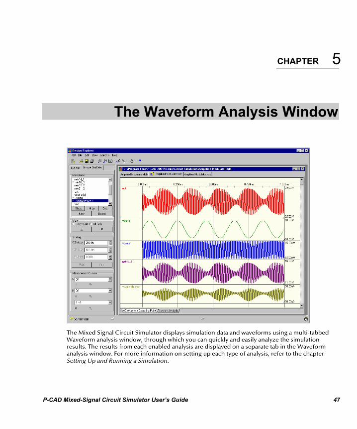
P-CAD Mixed-Signal Circuit Simulator User’s Guide 47
CHAPTER 5
The Waveform Analysis Window
The Mixed Signal Circuit Simulator displays simulation data and waveforms using a multi-tabbed Waveform analysis window, through which you can quickly and easily analyze the simulation results. The results from each enabled analysis are displayed on a separate tab in the Waveform analysis window. For more information on setting up each type of analysis, refer to the chapter Setting Up and Running a Simulation.
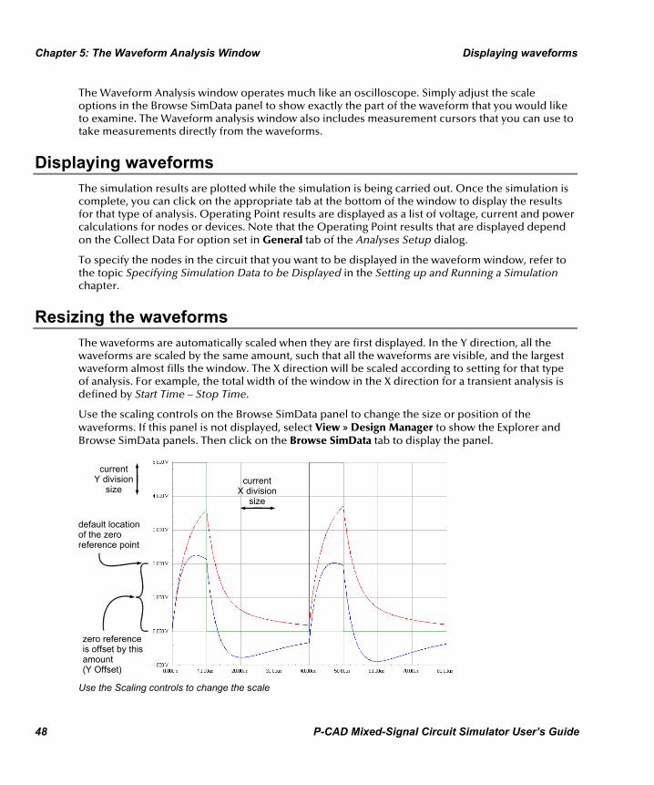
Chapter 5: The Waveform Analysis Window Displaying waveforms
48 P-CAD Mixed-Signal Circuit Simulator User’s Guide
The Waveform Analysis window operates much like an oscilloscope. Simply adjust the scale options in the Browse SimData panel to show exactly the part of the waveform that you would like to examine. The Waveform analysis window also includes measurement cursors that you can use to take measurements directly from the waveforms.
Displaying waveforms The simulation results are plotted while the simulation is being carried out. Once the simulation is complete, you can click on the appropriate tab at the bottom of the window to display the results for that type of analysis. Operating Point results are displayed as a list of voltage, current and power calculations for nodes or devices. Note that the Operating Point results that are displayed depend on the Collect Data For option set in General tab of the Analyses Setup dialog.
To specify the nodes in the circuit that you want to be displayed in the waveform window, refer to the topic Specifying Simulation Data to be Displayed in the Setting up and Running a Simulation chapter.
Resizing the waveforms The waveforms are automatically scaled when they are first displayed. In the Y direction, all the waveforms are scaled by the same amount, such that all the waveforms are visible, and the largest waveform almost fills the window. The X direction will be scaled according to setting for that type of analysis. For example, the total width of the window in the X direction for a transient analysis is defined by Start Time – Stop Time.
Use the scaling controls on the Browse SimData panel to change the size or position of the waveforms. If this panel is not displayed, select View » Design Manager to show the Explorer and Browse SimData panels. Then click on the Browse SimData tab to display the panel.
current Y division
size
default locationof the zero reference point
zero reference is offset by this amount(Y Offset)
current X division
size
Use the Scaling controls to change the scale
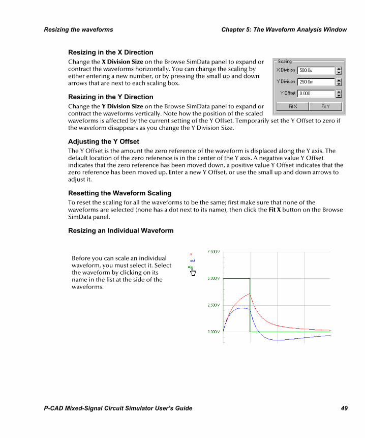
Resizing the waveforms Chapter 5: The Waveform Analysis Window
P-CAD Mixed-Signal Circuit Simulator User’s Guide 49
Resizing in the X Direction Change the X Division Size on the Browse SimData panel to expand or contract the waveforms horizontally. You can change the scaling by either entering a new number, or by pressing the small up and down arrows that are next to each scaling box.
Resizing in the Y Direction Change the Y Division Size on the Browse SimData panel to expand or contract the waveforms vertically. Note how the position of the scaled waveforms is affected by the current setting of the Y Offset. Temporarily set the Y Offset to zero if the waveform disappears as you change the Y Division Size.
Adjusting the Y Offset The Y Offset is the amount the zero reference of the waveform is displaced along the Y axis. The default location of the zero reference is in the center of the Y axis. A negative value Y Offset indicates that the zero reference has been moved down, a positive value Y Offset indicates that the zero reference has been moved up. Enter a new Y Offset, or use the small up and down arrows to adjust it.
Resetting the Waveform Scaling To reset the scaling for all the waveforms to be the same; first make sure that none of the waveforms are selected (none has a dot next to its name), then click the Fit X button on the Browse SimData panel.
Resizing an Individual Waveform
Before you can scale an individual waveform, you must select it. Select the waveform by clicking on its name in the list at the side of the waveforms.

Chapter 5: The Waveform Analysis Window Viewing waveforms in separate cells
50 P-CAD Mixed-Signal Circuit Simulator User’s Guide
Use the Scaling controls to re-scale the selected waveform only. You can change both the Y Division Size, and the Y Offset. In this example the Y Division size has been changed from 2.5V/div to 5V/div, and the Y Offset changed to move the “In” waveform up.
The “In” waveform has been de-selected by clicking on its name again. Note how the scale along the Y axis has disappeared, instead each name has its scale shown next to it. This only happens when they are scaled differently.
Viewing waveforms in separate cells To view the waveforms with each shown in a separate region (or cell), click on the All Cells option in the Browse SimData panel. Use this feature when you need to view digital signals separately.
How the waveforms appear in separate cells
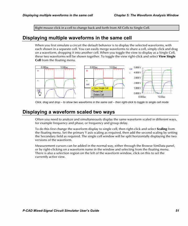
Displaying multiple waveforms in the same cell Chapter 5: The Waveform Analysis Window
P-CAD Mixed-Signal Circuit Simulator User’s Guide 51
Right mouse click in a cell to change back and forth from All Cells to Single Cell.
Displaying multiple waveforms in the same cell When you first simulate a circuit the default behavior is to display the selected waveforms, with each shown in a separate cell. You can easily merge waveforms to share a cell, simply click and drag on a waveform, dropping it into another cell. When you toggle the view to display as a Single Cell, these two waveforms will be shown together. To toggle the view right-click and select View Single Cell from the floating menu.
Click, drag and drop – to show two waveforms in the same cell – then right-click to toggle to single cell mode
Displaying a waveform scaled two ways Often you need to analyze and simultaneously display the same waveform scaled in different ways, for example frequency and phase, or frequency and group delay.
To do this first change the waveform display to single cell, then right-click and select Scaling from the floating menu. Set the primary Y axis scaling as required, then add the second scaling by setting the Secondary field as required. The single cell window will be split horizontally displaying the two versions of the waveform.
Measurement cursors can be added in the normal way, either through the Browse SimData panel, or by right-clicking on a waveform name in the window and selecting from the floating menu. There is also a selection region on the left of the waveform window, click on this to set the currently active view.
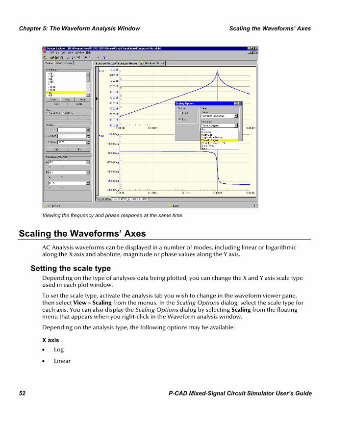
Chapter 5: The Waveform Analysis Window Scaling the Waveforms’ Axes
52 P-CAD Mixed-Signal Circuit Simulator User’s Guide
Viewing the frequency and phase response at the same time
Scaling the Waveforms’ Axes AC Analysis waveforms can be displayed in a number of modes, including linear or logarithmic along the X axis and absolute, magnitude or phase values along the Y axis.
Setting the scale type Depending on the type of analyses data being plotted, you can change the X and Y axis scale type used in each plot window.
To set the scale type, activate the analysis tab you wish to change in the waveform viewer pane, then select View » Scaling from the menus. In the Scaling Options dialog, select the scale type for each axis. You can also display the Scaling Options dialog by selecting Scaling from the floating menu that appears when you right-click in the Waveform analysis window.
Depending on the analysis type, the following options may be available:
X axis • Log
• Linear

Displaying the simulation data points Chapter 5: The Waveform Analysis Window
P-CAD Mixed-Signal Circuit Simulator User’s Guide 53
Y axis • Real
• Imaginary
• Magnitude
• Magnitude In Decibels
• Phase In Degrees
• Phase In Radians
• Group Delay.
Primary and Secondary Y axis To simultaneously view the same set of waveforms scaled in a different way, enable the Secondary Y axis in the Scaling Options dialog. The waveform display will be split horizontally, showing the two different scaling modes one above the other.
Note: Not all scaling options will be available for all data types.
Displaying the simulation data points If you are unsure about the accuracy of the waveforms (perhaps they look sharp and jagged instead of smooth and curved), you can turn on the simulation data points to check if the results have been calculated often enough.
To display the simulation data points, select View » Options from the menus and enable the Show Data Points option in the Document Options dialog. A small circle will be displayed at each point that data was calculated.
Identifying waveforms on a single color printout The Waveform analysis window includes a feature to easily identify each waveform on a single color printout. When you select View » Options from the menus, and enable the Show Designation Symbols option, identifier symbols are added to each waveform. If the waveforms are shown in individual cells, then all waveforms use a square symbol. If two or more waveforms share a cell, then a different shape is used for each waveform.

Chapter 5: The Waveform Analysis Window Using the Measurement Cursors
54 P-CAD Mixed-Signal Circuit Simulator User’s Guide
Use the designation symbols to clearly identify each waveform
Using the Measurement Cursors There are two measurement cursors that let you take measurements directly from the waveforms. You take measurements of time and amplitude from the transient analysis results, or find the frequency of the 3dB point from the AC small signal analysis results. You can also use the two cursors together to take difference measurements from two points on the same waveform, or two points on different waveforms.
Attach a cursor to a waveform by picking the waveform name in the list
Position the cursor by dragging the tab at the top of the window
Each of the two measurement cursors can be attached to any of the visible waveforms. To use the measurement cursors:

Using the Measurement Cursors Chapter 5: The Waveform Analysis Window
P-CAD Mixed-Signal Circuit Simulator User’s Guide 55
1. Select the waveform that you wish to attach a cursor to in the drop-down list.
2. A small tab with the letter of that cursor will appear at the top of the window. Click and drag this tab to change the location of the cursor.
3. Read the X and Y values of the current cursor point from the Measurement Cursors region of the Browse SimData panel.
How multi-pass results are displayed Monte Carlo, Parameter Sweep and Temperature Sweep actually perform multiple passes of the analysis, varying one or more circuit parameters with each pass. Each pass is identified by adding a letter and a number after the waveform name. The letter signifies the type of multi-pass analysis (m for Monte Carlo, t for temperature and p for parameter sweep), and the number signifies the pass. There is also a waveform for the simulation run which was done with the nominal circuit values, which does not have a character and number appended to its label. Following are some examples:
output-p1 Voltage at node output for Parameter Sweep run 1
output-p2 Voltage at node output for Parameter Sweep run 2
output-p3 Voltage at node output for Parameter Sweep run 3
output Voltage at node output for nominal run
output-m1 Voltage at node output for Monte Carlo run 1
output-t1 Voltage at node output for Temperature Sweep run 1.

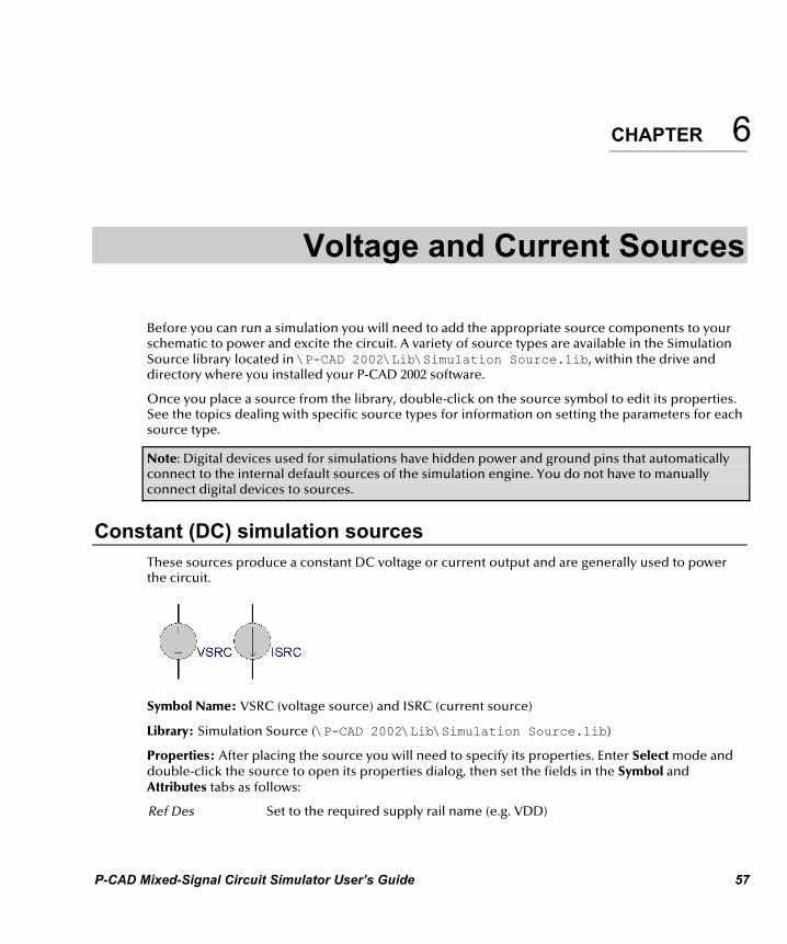
P-CAD Mixed-Signal Circuit Simulator User’s Guide 57
CHAPTER 6
Voltage and Current Sources
Before you can run a simulation you will need to add the appropriate source components to your schematic to power and excite the circuit. A variety of source types are available in the Simulation Source library located in \P-CAD 2002\Lib\Simulation Source.lib, within the drive and directory where you installed your P-CAD 2002 software.
Once you place a source from the library, double-click on the source symbol to edit its properties. See the topics dealing with specific source types for information on setting the parameters for each source type.
Note: Digital devices used for simulations have hidden power and ground pins that automatically connect to the internal default sources of the simulation engine. You do not have to manually connect digital devices to sources.
Constant (DC) simulation sources These sources produce a constant DC voltage or current output and are generally used to power the circuit.
Symbol Name: VSRC (voltage source) and ISRC (current source)
Library: Simulation Source (\P-CAD 2002\Lib\Simulation Source.lib)
Properties: After placing the source you will need to specify its properties. Enter Select mode and double-click the source to open its properties dialog, then set the fields in the Symbol and Attributes tabs as follows:
Ref Des Set to the required supply rail name (e.g. VDD)

Chapter 6: Voltage and Current Sources Sinusoidal source
58 P-CAD Mixed-Signal Circuit Simulator User’s Guide
Value Amplitude of the source voltage or current (e.g. 12)
SimField1 Magnitude of the small signal voltage. Set this if you plan to do a small signal AC analysis based on this source (typically 1). The prefix AC Magnitude= must be used when entering the value.
SimField2 Phase of the small signal voltage. The prefix AC Phase= must be used when entering the value.
Sinusoidal source Use these sources to create sinusoidal voltage and current waveforms.
Symbol Name: VSIN (voltage source) and ISIN (current source)
Library: Simulation Source (\P-CAD 2002\Lib\Simulation Source.lib)
Properties: After placing the source you will need to specify its properties. Enter Select mode and double-click the source to open its properties dialog, then set the fields in the Symbol and Attributes tabs as follows:
Ref Des Set to the required source name (e.g. INPUT)
SimField1 DC Magnitude. (Ignore this attribute. Alternatively, set the value F1:0 in the SimDefaults attribute)
SimField2 Magnitude of the small signal voltage. Set this if you plan to do an AC small signal analysis (typically 1). The prefix AC Magnitude= must be used when entering the value.
SimField3 Phase of the AC small signal voltage or current in degrees. The prefix AC Phase= must be used when entering the value.
SimField4 DC offset voltage or current. The prefix Offset= must be used when entering the value.
SimField5 Peak amplitude of the sinusoid (e.g. 100m). The prefix Amplitude= must be used when entering the value.
SimField6 Frequency of the sinusoidal voltage or current in Hz (e.g. 1000). The prefix Frequency= must be used when entering the value.
SimField7 Delay time until the source voltage commences in secs (e.g. 500u). The prefix Delay= must be used when entering the value.
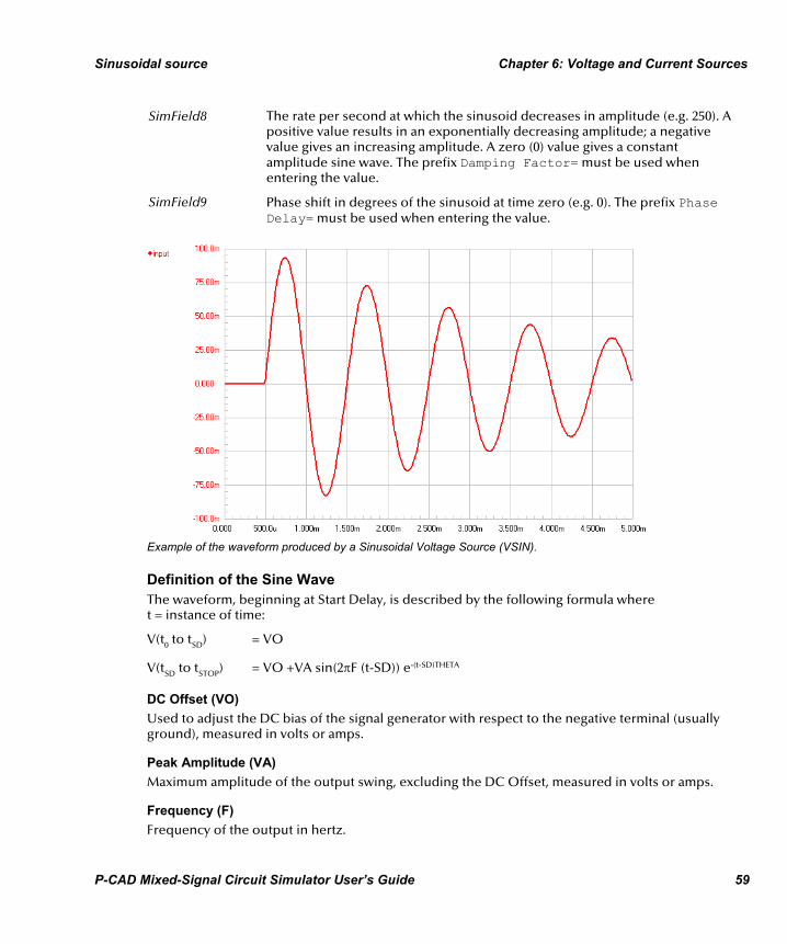
Sinusoidal source Chapter 6: Voltage and Current Sources
P-CAD Mixed-Signal Circuit Simulator User’s Guide 59
SimField8 The rate per second at which the sinusoid decreases in amplitude (e.g. 250). A positive value results in an exponentially decreasing amplitude; a negative value gives an increasing amplitude. A zero (0) value gives a constant amplitude sine wave. The prefix Damping Factor= must be used when entering the value.
SimField9 Phase shift in degrees of the sinusoid at time zero (e.g. 0). The prefix Phase Delay= must be used when entering the value.
Example of the waveform produced by a Sinusoidal Voltage Source (VSIN).
Definition of the Sine Wave The waveform, beginning at Start Delay, is described by the following formula where t = instance of time:
V(t0 to tSD) = VO
V(tSD to tSTOP) = VO +VA sin(2πF (t-SD)) e-(t-SD)THETA
DC Offset (VO) Used to adjust the DC bias of the signal generator with respect to the negative terminal (usually ground), measured in volts or amps.
Peak Amplitude (VA) Maximum amplitude of the output swing, excluding the DC Offset, measured in volts or amps.
Frequency (F) Frequency of the output in hertz.
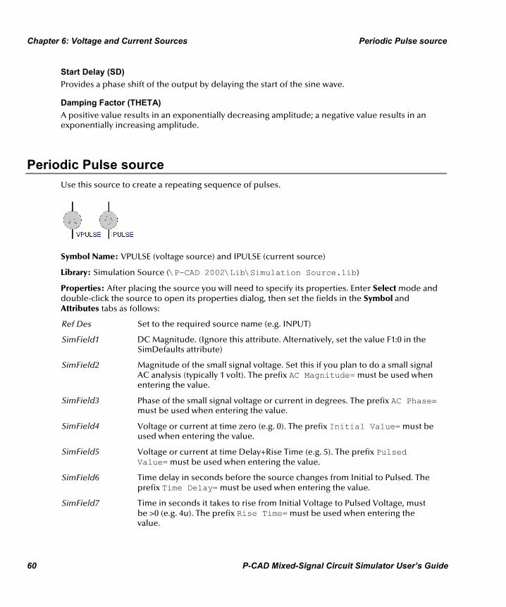
Chapter 6: Voltage and Current Sources Periodic Pulse source
60 P-CAD Mixed-Signal Circuit Simulator User’s Guide
Start Delay (SD) Provides a phase shift of the output by delaying the start of the sine wave.
Damping Factor (THETA) A positive value results in an exponentially decreasing amplitude; a negative value results in an exponentially increasing amplitude.
Periodic Pulse source Use this source to create a repeating sequence of pulses.
Symbol Name: VPULSE (voltage source) and IPULSE (current source)
Library: Simulation Source (\P-CAD 2002\Lib\Simulation Source.lib)
Properties: After placing the source you will need to specify its properties. Enter Select mode and double-click the source to open its properties dialog, then set the fields in the Symbol and Attributes tabs as follows:
Ref Des Set to the required source name (e.g. INPUT)
SimField1 DC Magnitude. (Ignore this attribute. Alternatively, set the value F1:0 in the SimDefaults attribute)
SimField2 Magnitude of the small signal voltage. Set this if you plan to do a small signal AC analysis (typically 1 volt). The prefix AC Magnitude= must be used when entering the value.
SimField3 Phase of the small signal voltage or current in degrees. The prefix AC Phase= must be used when entering the value.
SimField4 Voltage or current at time zero (e.g. 0). The prefix Initial Value= must be used when entering the value.
SimField5 Voltage or current at time Delay+Rise Time (e.g. 5). The prefix Pulsed Value= must be used when entering the value.
SimField6 Time delay in seconds before the source changes from Initial to Pulsed. The prefix Time Delay= must be used when entering the value.
SimField7 Time in seconds it takes to rise from Initial Voltage to Pulsed Voltage, must be >0 (e.g. 4u). The prefix Rise Time= must be used when entering the value.

Periodic Pulse source Chapter 6: Voltage and Current Sources
P-CAD Mixed-Signal Circuit Simulator User’s Guide 61
SimField8 Time in seconds it takes to fall from Pulsed Voltage back to Initial Voltage, must be >0 (e.g. 1u). The prefix Fall Time= must be used when entering the value.
SimField9 Time in seconds that the source remains at Pulsed Voltage (e.g. 0). The prefix Pulse Width= must be used when entering the value.
SimField10 Time in seconds between the start of the first pulse to the start of the second pulse (e.g. 5u). The prefix Period= must be used when entering the value.
SimField11 Phase delay in Degrees before the source changes from initial to Pulsed. The prefix Phase Delay= must be used when entering the value.
Example of the waveform produced by a Periodic Pulse Source.
Definition of the Pulse Shape The waveform is described as follows where t = instance of time. Intermediate points are set by linear interpolation:
V(t0) = VI
V(tSD) = VI
V(tSD+tTR) = VP
V(tSD+tTR+tPW) = VP
V(tSD+tTR+tPW+tTF) = VI
V(tSTOP) = VI
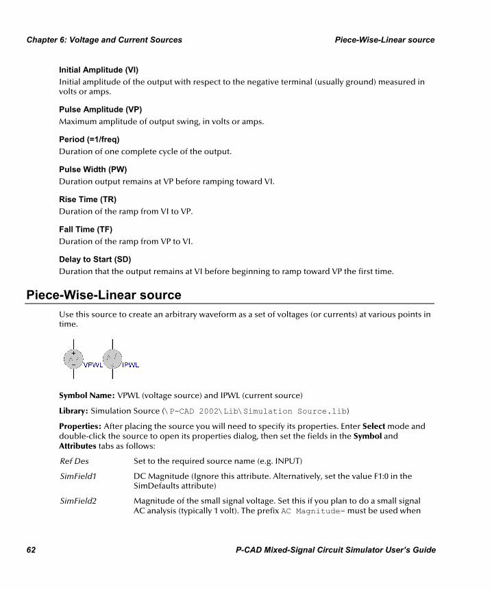
Chapter 6: Voltage and Current Sources Piece-Wise-Linear source
62 P-CAD Mixed-Signal Circuit Simulator User’s Guide
Initial Amplitude (VI) Initial amplitude of the output with respect to the negative terminal (usually ground) measured in volts or amps.
Pulse Amplitude (VP) Maximum amplitude of output swing, in volts or amps.
Period (=1/freq) Duration of one complete cycle of the output.
Pulse Width (PW) Duration output remains at VP before ramping toward VI.
Rise Time (TR) Duration of the ramp from VI to VP.
Fall Time (TF) Duration of the ramp from VP to VI.
Delay to Start (SD) Duration that the output remains at VI before beginning to ramp toward VP the first time.
Piece-Wise-Linear source Use this source to create an arbitrary waveform as a set of voltages (or currents) at various points in time.
Symbol Name: VPWL (voltage source) and IPWL (current source)
Library: Simulation Source (\P-CAD 2002\Lib\Simulation Source.lib)
Properties: After placing the source you will need to specify its properties. Enter Select mode and double-click the source to open its properties dialog, then set the fields in the Symbol and Attributes tabs as follows:
Ref Des Set to the required source name (e.g. INPUT)
SimField1 DC Magnitude (Ignore this attribute. Alternatively, set the value F1:0 in the SimDefaults attribute)
SimField2 Magnitude of the small signal voltage. Set this if you plan to do a small signal AC analysis (typically 1 volt). The prefix AC Magnitude= must be used when

Piece-Wise-Linear source Chapter 6: Voltage and Current Sources
P-CAD Mixed-Signal Circuit Simulator User’s Guide 63
entering the value.
SimField3 Phase in degrees of the small signal voltage. The prefix AC Phase= must be used when entering the value.
SimField4 Time-amplitude pairs. Enter up to eight pairs of numbers separated by spaces. The first number in a pair specifies the time in seconds, the second the voltage or current amplitude at that time (e.g. 0U 5V 5U 5V 12U 0V 50U 5V 60U 5V). The prefix Time/Current Pairs= must be used when entering the value for IPWL source. The prefix Time/Voltage Pairs= must be used when entering the value for VPWL source.
Example of the waveform produced by a PWL source with the Time/Voltage attribute set to 0U 5V 5U 5V 12U 0V 50U 5V 60U 5V
Definition of the Piece-Wise waveform Piecewise linear sources can take data from one of two sources:
1. You can describe the waveform with a set of up to 8 points that you enter directly into the SimField4 attribute (Time/Voltage or Time/Current) of the PWL source. The time specified for each successive point must be more positive than its predecessor. If it is not the cycle will end, excluding that and all successive points.
2. You can define the waveform in an ASCII text file containing an indefinite number of points. The file must be in the same directory, with the extension .PWL. Values must be entered in pairs: a time position followed by an amplitude. The first character of each data line must be a plus sign (+) and each line may contain up to 255 characters. Values must be separated by one or more spaces or tabs. Values may be entered in either scientific or engineering notation.

Chapter 6: Voltage and Current Sources Exponential sources
64 P-CAD Mixed-Signal Circuit Simulator User’s Guide
Comment lines may be added by making the first character of the line an asterisk (*). For example:
* Random Noise Data
+ 0.00000e-3 0.6667 0.00781e-3 0.6372 0.01563e-3 -0.1177
+ 0.02344e-3 -0.6058 0.03125e-3 0.2386 0.03906e-3 -1.1258
+ 0.04688e-3 1.6164 0.05469e-3 -0.3136 0.06250e-3 -1.0934
Note: If you are defining the waveform using this .PWL file, you will need to add the attribute SimField5 and declare the filename in the Value field in either of the following formats:
FILE= fullpathname\MyFile.PWL
FILE= {Model_Path}\anyotherpath\MyFile.PWL
The file can only be declared using SimField5. The Simulator checks this attribute for any file declaration. If no file has been declared, it uses the value specified in SimField4.
Exponential sources Use this source to create a pulse waveform with an exponential rising and/or falling edge.
Symbol Name: VEXP (voltage source) and IEXP (current source)
Library: Simulation Source (\P-CAD 2002\Lib\Simulation Source.lib)
Properties: After placing the source you will need to specify its properties. Enter Select mode and double-click the source to open its properties dialog, then set the fields in the Symbol and Attributes tabs as follows:
Ref Des Set to the required source name (e.g. INPUT)
SimField1 DC Magnitude (Ignore this attribute. Alternatively, set the value F1:0 in the SimDefaults attribute)
SimField2 Magnitude of the small signal voltage. Set this if you plan to do a small signal AC analysis (typically 1 volt/amp). The prefix AC Magnitude= must be used when entering the value.
SimField3 Phase in degrees of the small signal voltage or current. The prefix AC Phase= must be used when entering the value.
SimField4 Voltage or current amplitude at time zero (e.g. 0). The prefix Initial Value= must be used when entering the value.

Exponential sources Chapter 6: Voltage and Current Sources
P-CAD Mixed-Signal Circuit Simulator User’s Guide 65
SimField5 Maximum amplitude of the output swing (e.g. 5). The prefix Pulsed Value= must be used when entering the value.
SimField6 Delay in seconds before the source starts changing from Initial Value to Pulse Value (e.g. 1u). The prefix Rise Delay= must be used when entering the value.
SimField7 RC charging time constant in seconds (e.g. 700n). The prefix Rise Time= must be used when entering the value.
SimField8 Time in seconds at which the signal starts to fall from Pulse Value back to Initial Value, must be >0 (e.g. 2u). The prefix Fall Delay= must be used when entering the value.
SimField9 RC discharging time constant in seconds (e.g. 300n). The prefix Fall Time= must be used when entering the value.
Example of the waveform produced by an Exponential Source.
Definition of the Exponential Waveform The waveform is described by the following formulas, where t = instance of time:
V(t0 to tRD) = VI
V(tRD to tFD) = VI + (VP - VI) (1 - e-(t - tRD) / tRT)
V(tFD to tSTOP) = VI + (VP - VI) (-e-(t - tRD) / tRT) + (VI - VP) (1 - e-(t - tFD) / tFT)
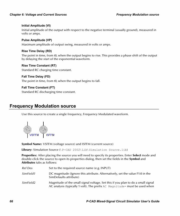
Chapter 6: Voltage and Current Sources Frequency Modulation source
66 P-CAD Mixed-Signal Circuit Simulator User’s Guide
Initial Amplitude (VI) Initial amplitude of the output with respect to the negative terminal (usually ground), measured in volts or amps.
Pulse Amplitude (VP) Maximum amplitude of output swing, measured in volts or amps.
Rise Time Delay (RD) The point in time, from t0, when the output begins to rise. This provides a phase shift of the output by delaying the start of the exponential waveform.
Rise Time Constant (RT) Standard RC charging time constant.
Fall Time Delay (FD) The point in time, from t0, when the output begins to fall.
Fall Time Constant (FT) Standard RC discharging time constant.
Frequency Modulation source Use this source to create a single frequency, Frequency Modulated waveform.
Symbol Name: VSFFM (voltage source) and ISFFM (current source)
Library: Simulation Source (\P-CAD 2002\Lib\Simulation Source.lib)
Properties: After placing the source you will need to specify its properties. Enter Select mode and double-click the source to open its properties dialog, then set the fields in the Symbol and Attributes tabs as follows:
Ref Des Set to the required source name (e.g. INPUT)
SimField1 DC magnitude (Ignore this attribute. Alternatively, set the value F1:0 in the SimDefaults attribute)
SimField2 Magnitude of the small signal voltage. Set this if you plan to do a small signal AC analysis (typically 1 volt). The prefix AC Magnitude= must be used when
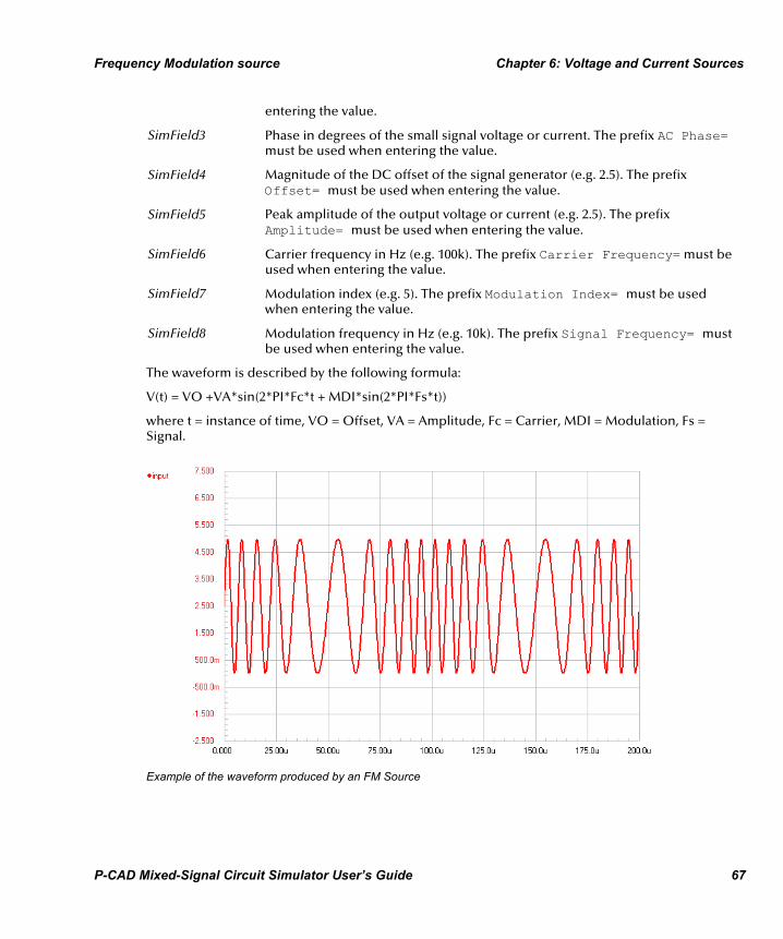
Frequency Modulation source Chapter 6: Voltage and Current Sources
P-CAD Mixed-Signal Circuit Simulator User’s Guide 67
entering the value.
SimField3 Phase in degrees of the small signal voltage or current. The prefix AC Phase= must be used when entering the value.
SimField4 Magnitude of the DC offset of the signal generator (e.g. 2.5). The prefix Offset= must be used when entering the value.
SimField5 Peak amplitude of the output voltage or current (e.g. 2.5). The prefix Amplitude= must be used when entering the value.
SimField6 Carrier frequency in Hz (e.g. 100k). The prefix Carrier Frequency= must be used when entering the value.
SimField7 Modulation index (e.g. 5). The prefix Modulation Index= must be used when entering the value.
SimField8 Modulation frequency in Hz (e.g. 10k). The prefix Signal Frequency= must be used when entering the value.
The waveform is described by the following formula:
V(t) = VO +VA*sin(2*PI*Fc*t + MDI*sin(2*PI*Fs*t))
where t = instance of time, VO = Offset, VA = Amplitude, Fc = Carrier, MDI = Modulation, Fs = Signal.
Example of the waveform produced by an FM Source

Chapter 6: Voltage and Current Sources Linear Dependent sources
68 P-CAD Mixed-Signal Circuit Simulator User’s Guide
Definition of the FM Waveform The waveform is described by the following formula where t = instance of time:
V(t) = VO +VA sin(2πFCt + MDI sin(2πFSt))
DC Offset (VO) Adjust the DC bias of the signal generator with respect to the negative terminal (usually ground), measured in volts or amps.
Peak Amplitude (VA) Maximum amplitude of the output swing, excluding the DC Offset, measured in volts or amps.
Carrier Frequency (FC) Frequency of the unmodulated output in hertz.
Modulation Index (MDI) Value corresponding to a function of amplitude of the modulating signal indicating the level of modulation. MDI = (frequency deviation) / FS
Signal Frequency (FS) Frequency of the modulating signal in hertz.
Linear Dependent sources Standard SPICE linear dependant sources are supported. Each linear dependant source has two input terminals and two output terminals. The voltage/current at the output terminals is a linear function of the voltage/current at the input terminals, dependant on the gain/transconductance/ transresistance of the source.
Symbol Name: GSRC (Voltage-Controlled Current Source) ESRC (Voltage-Controlled Voltage Source) FSRC (Current-Controlled Current Source) HSRC (Current-Controlled Voltage Source)
Library: Simulation Source (\P-CAD 2002\Lib\Simulation Source.lib)
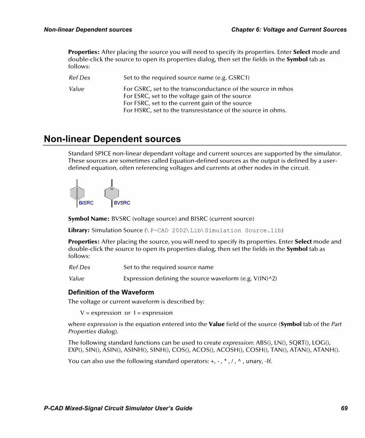
Non-linear Dependent sources Chapter 6: Voltage and Current Sources
P-CAD Mixed-Signal Circuit Simulator User’s Guide 69
Properties: After placing the source you will need to specify its properties. Enter Select mode and double-click the source to open its properties dialog, then set the fields in the Symbol tab as follows:
Ref Des Set to the required source name (e.g. GSRC1)
Value For GSRC, set to the transconductance of the source in mhos For ESRC, set to the voltage gain of the source For FSRC, set to the current gain of the source For HSRC, set to the transresistance of the source in ohms.
Non-linear Dependent sources Standard SPICE non-linear dependant voltage and current sources are supported by the simulator. These sources are sometimes called Equation-defined sources as the output is defined by a user-defined equation, often referencing voltages and currents at other nodes in the circuit.
Symbol Name: BVSRC (voltage source) and BISRC (current source)
Library: Simulation Source (\P-CAD 2002\Lib\Simulation Source.lib)
Properties: After placing the source, you will need to specify its properties. Enter Select mode and double-click the source to open its properties dialog, then set the fields in the Symbol tab as follows:
Ref Des Set to the required source name
Value Expression defining the source waveform (e.g. V(IN)^2)
Definition of the Waveform The voltage or current waveform is described by:
V = expression or I = expression
where expression is the equation entered into the Value field of the source (Symbol tab of the Part Properties dialog).
The following standard functions can be used to create expression: ABS(), LN(), SQRT(), LOG(), EXP(), SIN(), ASIN(), ASINH(), SINH(), COS(), ACOS(), ACOSH(), COSH(), TAN(), ATAN(), ATANH().
You can also use the following standard operators: +, - , * , / , ^ , unary, -If.

Chapter 6: Voltage and Current Sources F/V Converter simulation source
70 P-CAD Mixed-Signal Circuit Simulator User’s Guide
To reference in an equation the voltage or current at a node in your circuit, you must use the name defined in the Net Name field of the Net Information dialog (select node and right click and choose Net Info from the popup menu) to reference the node using the following syntax:
V(Net) references the voltage at node Net
I(Net) references the current at the node Net
For example, if you have a node in your circuit labeled with a Net Name called IN, then the following would be valid entries in the Value field of the source:
V(IN)^3
COS(V(IN))
If the argument of a LOG(), LN(), or SQRT() function becomes less than zero, the absolute value of the argument is used. If a divisor becomes zero, or the argument of log or ln becomes zero, an error will result. Other problems may occur when the argument for a function in a partial derivative enters a region where that function is undefined.
F/V Converter simulation source The simulator supports a frequency to voltage converter.
Symbol Name: FTOV
Library: Miscellaneous Devices (\P-CAD 2002\Lib\Miscellaneous Devices.lib)
Properties: After placing the source you will need to specify its properties. Enter Select mode and double-click the source to open its properties dialog, then set the fields in the Symbol and Attributes tabs as follows:
Ref Des Set to the required source name (e.g. FTOV1)
SimField1 Low level input threshold. The prefix VIL= must be used when entering the value.
SimField2 High level input threshold. The prefix VIH= must be used when entering the value.
SimField3 Cycles per volt output. The prefix CYCLES= must be used when entering the value.
The output is a voltage, the level of which is a linear function of the input frequency.
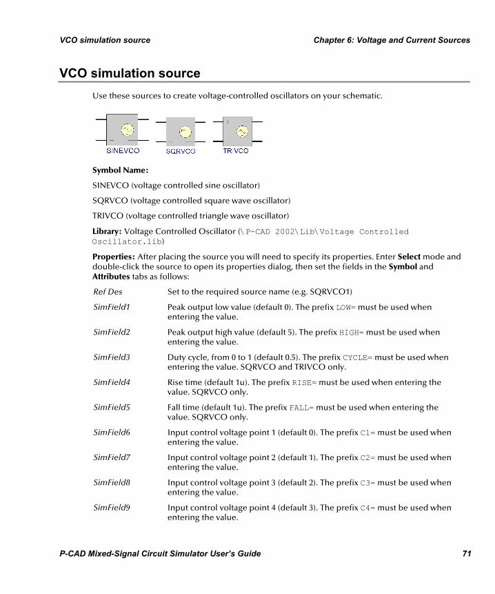
VCO simulation source Chapter 6: Voltage and Current Sources
P-CAD Mixed-Signal Circuit Simulator User’s Guide 71
VCO simulation source Use these sources to create voltage-controlled oscillators on your schematic.
Symbol Name:
SINEVCO (voltage controlled sine oscillator)
SQRVCO (voltage controlled square wave oscillator)
TRIVCO (voltage controlled triangle wave oscillator)
Library: Voltage Controlled Oscillator (\P-CAD 2002\Lib\Voltage Controlled Oscillator.lib)
Properties: After placing the source you will need to specify its properties. Enter Select mode and double-click the source to open its properties dialog, then set the fields in the Symbol and Attributes tabs as follows:
Ref Des Set to the required source name (e.g. SQRVCO1)
SimField1 Peak output low value (default 0). The prefix LOW= must be used when entering the value.
SimField2 Peak output high value (default 5). The prefix HIGH= must be used when entering the value.
SimField3 Duty cycle, from 0 to 1 (default 0.5). The prefix CYCLE= must be used when entering the value. SQRVCO and TRIVCO only.
SimField4 Rise time (default 1u). The prefix RISE= must be used when entering the value. SQRVCO only.
SimField5 Fall time (default 1u). The prefix FALL= must be used when entering the value. SQRVCO only.
SimField6 Input control voltage point 1 (default 0). The prefix C1= must be used when entering the value.
SimField7 Input control voltage point 2 (default 1). The prefix C2= must be used when entering the value.
SimField8 Input control voltage point 3 (default 2). The prefix C3= must be used when entering the value.
SimField9 Input control voltage point 4 (default 3). The prefix C4= must be used when entering the value.

Chapter 6: Voltage and Current Sources VCO simulation source
72 P-CAD Mixed-Signal Circuit Simulator User’s Guide
SimField10 Input control voltage point 5 (default 4). The prefix C5= must be used when entering the value.
SimField11 Output frequency point 1 (default 0). The prefix F1= must be used when entering the value.
SimField12 Output frequency point 2 (default 1k). The prefix F2= must be used when entering the value.
SimField13 Output frequency point 3 (default 2k). The prefix F3= must be used when entering the value.
SimField14 Output frequency point 4 (default 3k). The prefix F4= must be used when entering the value.
SimField15 Output frequency point 5 (default 4k).The prefix F5= must be used when entering the value.
The parameters C1, C2,... and F1, F2,... define the voltage to frequency conversion function. The C values define input voltage levels and the F values set the respective output frequencies generated for these input levels. Linear interpolation is used to define input/output values between the set points.
P-CAD Mixed-Signal Circuit Simulator User’s Guide 73
CHAPTER 7
Components and Models
The simulator uses the standard SPICE syntax to describe the analog devices used in the circuit. In most cases, you simply place a component from the library, set the value (such as the resistance) and simulate. Each simulation-ready component includes all the information required for simulation, including designator prefix information and pin mapping for multi-part components.
SPICE also supports many extended features that allow you to more accurately model component behavior. For example, you may need to simulate a resistor based on geometric information, or specify the operating temperature of a transistor.
This extra information is entered as component simulation attributes after the component has been placed on the schematic sheet. Refer to the Device Descriptions topic later in this chapter for a description of what information is entered in each attribute for each type of device.
You can also create your own simulation-ready schematic symbols. Refer to the topic Creating your own Simulation-Ready Components for more information on linking a schematic symbol to a model.
Selecting simulation-ready components All components/parts placed on your schematic must contain special simulation-specific information that tells the simulator how these components/parts are to be treated when running an analysis. In general, this means that schematic components/parts must include a reference to an appropriate SPICE device model.
The simulation models can be found in \Design Explorer 99 SE\Library\Sim\ within the drive and directory where you installed your Design Explorer 99 SE software. All of the models are stored in folders relating to the manufacturer of the component.
There are over 27,000 components in the collection of libraries associated with P-CAD. Of these, over 6,000 have a simulation model associated to them. There are two ways that you can find out whether a particular component in a P-CAD library has an associated simulation model:
• Place a part from a library and examine the Attributes tab of the Properties dialog. If the part has an associated simulation model file, the attribute SimModel will exist and also the attribute SimFile will be apparent with an entry pointing to a .mdl or .ckt file. In some cases, the part

Chapter 7: Components and Models Simulation-ready Resistors
74 P-CAD Mixed-Signal Circuit Simulator User’s Guide
may be simulatable without pointing to a model. If this is the case, then there will be attribute entries for SimType, SimPins and SimNetlist.
• Open the Library Index spreadsheet, which can be found in \P-CAD 2002\Lib\Library Index.xls within the drive and directory where you installed your P-CAD 2002 software. From here you can search all of the components in all of the P-CAD libraries, to determine which are simulatable, i.e. have a simulation model associated to them.
SPICE supports many extended features that allow you to more accurately model component behavior, e.g. specifying the operating temperature of a transistor. This extra information is entered into the SimField attributes of the Part Properties dialog after the part has been placed on the schematic sheet. To edit a part's properties, double-click on the part's symbol, making sure you are in Select mode first.
Models and Subcircuits The simulator’s SPICE engine has built-in models for the following analog component types; resistors, capacitors, inductors, mutual inductors, independent voltage and current sources, dependent sources, lossless and lossy transmission lines, switches, uniform distributed RC lines, and the five most common semiconductor devices; diodes, BJTs, JFETs, MESFETs, and MOSFETs. The simulator also includes a large number of model files that define the behavior of specific instances of these devices. These model files normally have the file extension .MDL. All the simulation models and subcircuits are stored in \Design Explorer 99 SE\Library\Sim\.
The simulator also supports the description of more complex devices, such as op amps, regulators, timers, crystals, etc, using the hierarchical subcircuit syntax. A subcircuit consists of SPICE elements that are defined and referenced in a fashion similar to device models. There is no limit on the size or complexity of subcircuits, and subcircuits can call other subcircuits. Each subcircuit is defined in a subcircuit file (*.CKT), which are also often referred to as “models”.
Device Descriptions Apart from discrete components (such as resistors), the component Type is used as the reference to the simulation model. For non-discrete components (op amps, etc) you should only change the Type value if you want to reference a different model.
Simulation-ready Resistors The General Devices library (\P-CAD 2002\Lib\General Devices.lib) contains the following simulation-ready resistor symbols for use in schematics:
• RES (fixed resistor)
• RESSEMI (semiconductor resistor)
• RPOT (potentiometer)
• RVAR (variable resistor)

Simulation-ready Capacitors Chapter 7: Components and Models
P-CAD Mixed-Signal Circuit Simulator User’s Guide 75
These symbols represent generic resistor types. As well as standard fixed and variable resistors, semiconductor resistors are supported. Semiconductor resistors allow you to model the resistance as a function of the geometry, and specify the temperature at which the device is to operate.
These parts have special simulation properties fields. Enter Select mode and double-click the symbol after placement to open its Properties dialog, then set the fields in the Symbol and Attributes tabs as follows:
Ref Des Resistor designator (e.g. R1)
Value Resistor value in ohms (e.g. 100k). For RESSEMI, if a value is specified in this field it overrides the geometric definition
SimField1 Optional. Length of the resistor in meters. The prefix L= must be used when entering the value (RESSEMI only)
SimField2 Optional. Width of the resistor in meters. The prefix W= must be used when entering the value (RESSEMI only)
SimField3 Optional. Temperature in degrees Celsius at which the device is to operate - default is 27. The prefix TEMP= must be used when entering the value (RESSEMI only)
SimField4 Set point for variable resistors. The prefix SET= must be used when entering the value (RPOT and RVAR only)
Values marked as ‘Optional’ include default values that should be applicable to most simulations. Generally you do not need to change these values.
Simulation-ready Capacitors The General Devices library (\P-CAD 2002\Lib\General Devices.lib) contains the following simulation-ready capacitor symbols for use in schematics:
• CAP (fixed, non-polarized capacitor)
• CAP2 (fixed, polarized capacitor)
• CAPBP (fixed, bi-polar capacitor)
• CAPSEMI (semiconductor capacitor)
These symbols represent generic capacitor types. As well as standard polarized, non-polarized and bi-polar capacitors, semiconductor capacitors are supported. Semiconductor capacitors allow you to model the capacitance as a function of the geometry.
These parts have special simulation properties fields. Enter Select mode and double-click the symbol after placement to open its Properties dialog, then set the fields in the Symbol and Attributes tabs as follows:
Ref Des Capacitor designator (e.g. C2)
Value Capacitor value in Farads (e.g. 22u). For CAPSEMI, if a value is specified in this

Chapter 7: Components and Models Simulation-ready Inductors
76 P-CAD Mixed-Signal Circuit Simulator User’s Guide
field it overrides the geometric definition
SimField1 Optional. Length of the capacitor in meters. The prefix L= must be used when entering the value (CAPSEMI only)
SimField2 Optional. Width of the capacitor in meters. The prefix W= must be used when entering the value (CAPSEMI only)
SimField3 Optional. Initial Conditions – time-zero voltage of capacitor. The prefix IC= must be used when entering the value. Only applies if the Use Initial Conditions option is enabled in the Transient/Fourier tab of the Setup Analyses dialog (Simulate » Setup).
Values marked as ‘Optional’ include default values that should be applicable to most simulations. Generally you do not need to change these values.
Simulation-ready Inductors The General Devices library (\P-CAD 2002\Lib\General Devices.lib) contains the following simulation-ready inductor symbol for use in schematics:
• INDUCTOR
This part has special simulation properties fields. Enter Select mode and double-click the symbol after placement to open its Properties dialog, then set the fields in the Symbol and Attributes tabs as follows:
Ref Des Inductor designator (e.g. L1)
Value Inductor value in Henrys (e.g. 47u)
SimField1 Optional. Initial Conditions – time-zero current flowing through inductor. The prefix IC= must be used when entering the value. Only applies if the Use Initial Conditions option is enabled in the Transient/Fourier tab of the Setup Analyses dialog (Simulate » Setup).
Values marked as ‘Optional’ include default values that should be applicable to most simulations. Generally you do not need to change these values.
Coupled Inductors
For an example of how coupled inductors are specified in the attributes, look at the TRANS2 component in General Devices.Lib. This is a transformer that is based on the coupled inductor model. You can see how the coupled inductors are declared in the SimNetlist attribute of the Attributes tab.
Simulation-ready Diodes The P-CAD libraries contain a comprehensive list of simulation-ready diodes. Use the Library Index spreadsheet (\P-CAD 2002\Lib\Library Index.xls) to locate the particular simulatable diode

Simulation-ready BJTs Chapter 7: Components and Models
P-CAD Mixed-Signal Circuit Simulator User’s Guide 77
you require and the associated library where the part is stored (e.g. Silicon Rectifier Diode: Name = 1N1183; Library = IR Discrete Diode.lib).
These parts have special simulation properties fields. Enter Select mode and double-click the symbol after placement to open its Properties dialog, then set the fields in the Symbol and Attributes tabs as follows:
Ref Des Diode designator (e.g. D1)
SimField1 Optional. Area factor specifies the number of equivalent parallel devices of the specified model. The prefix AREA= must be used when entering the value. This setting affects a number of parameters in the model.
SimField2 Optional. Set to “Off” to set diode voltage to zero during operating point analysis. The prefix ON/OFF= must be used when entering the value. Can be useful as an aid in convergence.
SimField3 Optional. Initial Conditions – time-zero voltage across the diode. The prefix IC= must be used when entering the value. Only applies if the Use Initial Conditions option is enabled in the Transient/Fourier tab of the Setup Analyses dialog (Simulate » Setup).
SimField4 Optional. Temperature in degrees Celsius at which this device is to operate (default is 27 deg.). The prefix TEMP= must be used when entering the value.
Values marked as ‘Optional’ include default values that should be applicable to most simulations. Generally, you do not need to change these values.
Simulation-ready BJTs The P-CAD libraries contain a comprehensive list of simulation-ready BJTs. Use the Library Index spreadsheet (\P-CAD 2002\Lib\Library Index.xls) to locate the particular simulatable BJT you require and the associated library where the part is stored (e.g. Amplifier Transistor NPN Silicon: Name = 2N930; Library = Motorola Discrete BJT.lib).
The model for the BJT is based on the integral-charge model of Gummel and Poon. However, if the Gummel-Poon parameters are not specified, the model reduces to the simpler Ebers-Moll model.
These parts have special simulation properties fields. Enter Select mode and double-click the symbol after placement to open its Properties dialog, then set the fields in the Symbol and Attributes tabs as follows:
Ref Des Transistor designator (e.g. Q1)
SimField1 Optional. Area factor specifies the number of equivalent parallel devices of the specified model. The prefix AREA= must be used when entering the value. This setting affects a number of parameters in the model.
SimField2 Optional. Set to “Off” to set terminal voltages to zero during operating point analysis. The prefix ON/OFF= must be used when entering the value. Can be useful as an aid in convergence.
Chapter 7: Components and Models Simulation-ready JFETs
78 P-CAD Mixed-Signal Circuit Simulator User’s Guide
SimField3 Optional. Initial Conditions – time-zero current flowing through inductor. The prefix IC= must be used when entering the value. Only applies if the Use Initial Conditions option is enabled in the Transient/Fourier tab of the Setup Analyses dialog (Simulate » Setup).
SimField4 Optional. Temperature in degrees Celsius at which this device is to operate (default is 27 deg.). The prefix TEMP= must be used when entering the value.
Values marked as ‘Optional’ include default values that should be applicable to most simulations. Generally, you do not need to change these values.
Simulation-ready JFETs The P-CAD libraries contain a comprehensive list of simulation-ready JFETs. Use the Library Index spreadsheet (\P-CAD 2002\Lib\Library Index.xls) to locate the particular simulatable JFET you require and the associated library where the part is stored (e.g. JFETs General Purpose: Name = 2N5457; Library = Motorola Discrete JFET.lib).
The JFET model is based on the FET model of Shichman and Hodges.
These parts have special simulation properties fields. Enter Select mode and double-click the symbol after placement to open its Properties dialog, then set the fields in the Symbol and Attributes tabs as follows:
Ref Des Transistor designator (e.g. Q1)
SimField1 Optional. Area factor specifies the number of equivalent parallel devices of the model. The prefix AREA= must be used when entering the value. This setting affects a number of parameters in the model.
SimField2 Optional. Set to “Off” to set terminal voltages to zero during operating point analysis. The prefix ON/OFF= must be used when entering the value. Can be useful as an aid in convergence.
SimField3 Optional. Initial Conditions – time-zero current flowing through inductor. The prefix IC= must be used when entering the value. Only applies if the Use Initial Conditions option is enabled in the Transient/Fourier tab of the Setup Analyses dialog (Simulate » Setup).
SimField4 Optional. Temperature in degrees Celsius at which this device is to operate (default is 27 deg.). The prefix TEMP= must be used when entering the value.
Values marked as ‘Optional’ include default values that should be applicable to most simulations. Generally you do not need to change these values.
Simulation-ready MOSFETs The P-CAD libraries contain a comprehensive list of simulation-ready MOSFETs. Use the Library Index spreadsheet (\P-CAD 2002\Lib\Library Index.xls) to locate the particular simulatable

Simulation-ready MOSFETs Chapter 7: Components and Models
P-CAD Mixed-Signal Circuit Simulator User’s Guide 79
MOSFET you require and the associated library where the part is stored (e.g. TMOS Dual N Channel Field Effect Transistor: Name = MMDF1N05E; Library = Motorola Discrete MOSFET.lib).
The simulation engine supports Shichman Hodges, BSIM 1, 2 and 3, and MOS 2, 3 and 6 models.
These parts have special simulation properties fields. Enter Select mode and double-click the symbol after placement to open its Properties dialog, then set the fields in the Symbol and Attributes tabs as follows:
Ref Des Transistor designator (e.g. Q1)
SimField1 Optional. Channel length (meters). The prefix L= must be used when entering the value.
SimField2 Optional. Channel width (meters). The prefix W= must be used when entering the value.
SimField3 Optional. Drain area (sq.meters). The prefix AD= must be used when entering the value.
SimField4 Optional. Source area (sq.meters). The prefix AS= must be used when entering the value.
SimField5 Optional. Perimeter of drain junction (meters). The prefix PD= must be used when entering the value.
SimField6 Optional. Perimeter of source junction (meters). The prefix PS= must be used when entering the value.
SimField7 Optional. Equivalent no. of drain diffusions. The prefix NRD= must be used when entering the value.
SimField8 Optional. Equivalent no. of source diffusions. The prefix NRS= must be used when entering the value.
SimField9 Optional. Set to “Off” to set terminal voltages to zero during operating point analysis. The prefix ON/OFF= must be used when entering the value. Can be useful as an aid in convergence.
SimField10 Optional. Initial Conditions – time-zero current flowing through inductor. The prefix IC= must be used when entering the value. Only applies if the Use Initial Conditions option is enabled in the Transient/Fourier tab of the Setup Analyses dialog (Simulate » Setup).
SimField11 Optional. Temperature in degrees Celsius at which this device is to operate (default is 27 deg.). The prefix TEMP= must be used when entering the value.
Values marked as ‘Optional’ include default values that should be applicable to most simulations. Generally you do not need to change these values.

Chapter 7: Components and Models Simulation-ready MESFETs
80 P-CAD Mixed-Signal Circuit Simulator User’s Guide
Simulation-ready MESFETs The Discrete Devices library (\P-CAD 2002\Lib\Discrete Devices.lib) contains generic MESFET transistor symbols.
The MESFET model is derived from the GaAs FET model of Statz.
These parts have special simulation properties fields. Enter Select mode and double-click the symbol after placement to open its Properties dialog, then set the fields in the Symbol and Attributes tabs as follows:
Ref Des Transistor designator (e.g. Q1)
SimField1 Optional. Area factor specifies the number of equivalent parallel devices of the model. The prefix AREA= must be used when entering the value. This setting affects a number of parameters in the model.
SimField2 Optional. Set to “Off” to set terminal voltages to zero during operating point analysis. The prefix ON/OFF= must be used when entering the value. Can be useful as an aid in convergence.
SimField3 Optional. Initial Conditions – time-zero current flowing through inductor. The prefix IC= must be used when entering the value. Only applies if the Use Initial Conditions option is enabled in the Transient/Fourier tab of the Setup Analyses dialog (Simulate » Setup).
Values marked as ‘Optional’ include default values that should be applicable to most simulations. Generally you do not need to change these values.
Simulation-ready V/I Controlled Switches The P-CAD libraries contain a comprehensive list of simulation-ready switches (Current and Voltage controlled). Use the Library Index spreadsheet (\P-CAD 2002\Lib\Library Index.xls) to locate the particular simulatable switch you require and the associated library where the part is stored (e.g. Current Controlled Switch: Name = ISW; Library = Miscellaneous Devices.lib).
These parts have special simulation properties fields. Enter Select mode and double-click the symbol after placement to open its Properties dialog, then set the fields in the Symbol and Attributes tabs as follows:
Ref Des Switch designator (e.g. S1)
SimField1 Optional. Initial switch condition. Set to either ON or OFF. The prefix ON/OFF= must be used when entering the value.
Values marked as ‘Optional’ include default values that should be applicable to most simulations. Generally you do not need to change these values.
Note: The use of an ideal, highly non-linear element such as a switch can cause large discontinuities to occur in the circuit node voltages. This can cause numerical round off or
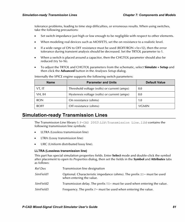
Simulation-ready Transmission Lines Chapter 7: Components and Models
P-CAD Mixed-Signal Circuit Simulator User’s Guide 81
tolerance problems, leading to time step difficulties, or erroneous results. When using switches, take the following precautions:
• Set switch impedance just high or low enough to be negligible with respect to other elements.
• When modeling real devices such as MOSFETS, set the on resistance to a realistic level.
• If a wide range of ON to OFF resistance must be used (ROFF/RON >1e+12), then the error tolerance during transient analysis should be decreased. Set the TRTOL parameter to 1.
• When a switch is placed around a capacitor, then the CHGTOL parameter should also be reduced (try 1e-16).
• To adjust the TRTOL and CHGTOL parameters from the schematic, select Simulate » Setup and then click the Advanced button in the Analyses Setup dialog.
Internally the SPICE engine supports the following switch parameters:
Name Parameter and Units Default Value
VT, IT Threshold voltage (volts) or current (amps) 0.0
VH, IH Hysteresis voltage (volts) or current (amps) 0.0
RON On resistance (ohms) 1.0
ROFF Off resistance (ohms) 1/GMIN
Simulation-ready Transmission Lines The Transmission Line library (\P-CAD 2002\Lib\Transmission Line.lib) contains the following transmission line symbols:
• LLTRA (Lossless transmission line)
• LTRA (Lossy transmission line)
• URC (Uniform distributed lossy line).
LLTRA (Lossless transmission line) This part has special simulation properties fields. Enter Select mode and double-click the symbol after placement to open its Properties dialog, then set the fields in the Symbol and Attributes tabs as follows:
Ref Des Transmission line designation
SimField1 Optional. Characteristic impedance (ohms). The prefix ZO= must be used when entering the value.
SimField2 Transmission delay. The prefix TD= must be used when entering the value.
SimField3 Frequency. The prefix F= must be used when entering the value.
Chapter 7: Components and Models Simulation-ready Transmission Lines
82 P-CAD Mixed-Signal Circuit Simulator User’s Guide
SimField4 Normalized electrical length of the transmission line with respect to the wavelength in the line, at the frequency F. The prefix NL= must be used when entering the value.
SimField5 Optional. Initial Conditions – time-zero current flowing through inductor. The prefix IC= must be used when entering the value. Only applies if the Use Initial Conditions option is enabled in the Transient/Fourier tab of the Setup Analyses dialog (Simulate » Setup).
The length of the line must be expressed in one of two forms: the transmission delay is specified directly (e.g. TD=10ns); alternatively, a frequency F is specified, together with the normalized length, NL. If a frequency is specified but NL is omitted then 0.25 is assumed (that is, the frequency is assumed to be the quarter-wave frequency).
Values marked as ‘Optional’ include default values that should be applicable to most simulations. Generally you do not need to change these values.
LTRA (Lossy transmission line) This uses a two-port convolution model for single-conductor lossy transmission lines. The model includes attributes for resistance, inductance, capacitance and length. It is not possible to pass these parameters directly from the schematic component, however you can create and reference your own model file. To do this, copy the file LTRA.mdl. Edit this new model file and change the string immediately after the .MODEL statement to be the same as the new file name, then edit the attributes as required. To use this new model from the schematic, enter the new model name (without extension) in the Type field of the Symbol tab in the Part Properties dialog.
For example, from the existing model file LTRA.mdl:
.MODEL LTRA LTRA(R=0.000 L=9.130n C=3.650p LEN=1.000)
You could create a new file, LTRA10.mdl:
.MODEL LTRA10 LTRA(R=0.2 L=32n C=13p LEN=10.000)
URC (Uniform distributed lossy line) This part has special simulation properties fields. Enter Select mode and double-click the symbol after placement to open its Properties dialog, then set the fields in the Symbol and Attributes tabs as follows:
Ref Des Transmission line designation
SimField1 Optional. Length of the RC line (meters). The prefix L= must be used when entering the value.
SimField2 Optional. Number of lumped segments to use in modeling the RC line. The prefix N= must be used when entering the value.
Values marked as ‘Optional’ include default values that should be applicable to most simulations. Generally you do not need to change these values.

Simulation-ready Transformers Chapter 7: Components and Models
P-CAD Mixed-Signal Circuit Simulator User’s Guide 83
Simulation-ready Transformers The General Devices library (\P-CAD 2002\Lib\General Devices.lib) contains symbols for a variety of transformer types. Those with the suffix CT represent center-tapped transformers.
These parts have special simulation properties fields. Enter Select mode and double-click the symbol after placement to open its Properties dialog, then set the fields in the Symbol and Attributes tabs as follows:
Ref Des Transformer designator (e.g. T1)
SimField1 Secondary/Primary turns ratio (e.g. 0.1). This overrides the model default. The prefix RATIO= must be used when entering the value. (Not CT types)
SimField2 Optional. Number of turns on the Primary. The prefix NP= must be used when entering the value.
SimField3 Optional. Number of turns on the Secondary, above center tap. The prefix NS1= must be used when entering the value.
SimField4 Optional. Number of turns on the Secondary, below center tap. The prefix NS2= must be used when entering the value.
Values marked as ‘Optional’ include default values that should be applicable to most simulations. Generally you do not need to change these values.
Simulation-ready Fuses The General Devices library (\P-CAD 2002\Lib\General Devices.lib) contains a symbol for a generic fuse device.
This part has special simulation properties fields. Enter Select mode and double-click the symbol after placement to open its Properties dialog, then set the fields in the Symbol and Attributes tabs as follows:
Ref Des Fuse designator (e.g. F1)
SimField1 Fuse current at rupture (e.g. 250m). The prefix CURRENT= must be used when entering the value.
SimField2 Optional. Series fuse resistance in ohms. The prefix RESISTANCE= must be used when entering the value.
Values marked as ‘Optional’ include default values that should be applicable to most simulations. Generally you do not need to change these values.
Simulation-ready Crystals The Crystal Oscillator library (\P-CAD 2002\Lib\Crystal Oscillator.lib) contains the symbol for a generic crystal device. For other crystal oscillators, use the Library Index spreadsheet
Chapter 7: Components and Models Simulation-ready Relays
84 P-CAD Mixed-Signal Circuit Simulator User’s Guide
(\P-CAD 2002\Lib\Library Index.xls) to locate the particular simulatable crystal oscillator you require and the associated library where the part is stored.
These parts have special simulation properties fields. Enter Select mode and double-click the symbol after placement to open its Properties dialog, then set the fields in the Symbol and Attributes tabs as follows:
Ref Des Crystal designator (e.g. Y1)
SimField1 Optional. Crystal frequency (e.g. 2.5M). The prefix FREQ= must be used when entering the value. This overrides the model default.
SimField2 Optional. Series resistance in ohms. The prefix RS= must be used when entering the value.
SimField3 Optional. Capacitance in Farads. The prefix C= must be used when entering the value.
SimField4 Optional. Q of the equivalent circuit. The prefix Q= must be used when entering the value.
Values marked as ‘Optional’ include default values that should be applicable to most simulations. Generally you do not need to change these values.
Simulation-ready Relays The Miscellaneous Devices library (\P-CAD 2002\Lib\Miscellaneous Devices.lib) contains a symbol for an SPDT relay type.
This part has special simulation properties fields. Enter Select mode and double-click the symbol after placement to open its Properties dialog, then set the fields in the Symbol and Attributes tabs as follows:
Ref Des Relay designator (e.g. RLY1)
SimField1 Optional. Contact pullin voltage. The prefix PULLIN= must be used when entering the value.
SimField2 Optional. Contact dropoff voltage. The prefix DROPOFF= must be used when entering the value.
SimField3 Optional. Contact resistance in ohms. The prefix CONTACT= must be used when entering the value.
SimField4 Optional. Coil resistance in ohms. The prefix RESISTANCE= must be used when entering the value.
SimField5 Optional. Coil inductance in Henrys. The prefix INDUCTANCE= must be used when entering the value.
Values marked as ‘Optional’ include default values that should be applicable to most simulations. Generally you do not need to change these values.
Simulation-ready integrated components Chapter 7: Components and Models
P-CAD Mixed-Signal Circuit Simulator User’s Guide 85
Simulation-ready integrated components Complex components are those that are fully modeled using a SPICE subcircuit and which have no user-definable settings. For these devices, you simply place the part from the library and set the designator. All simulation parameters are defined in the SPICE subcircuit used to model the device.
You can readily identify a component that is fully modeled using a SPICE subcircuit, by placing the part and then checking the Attributes tab of the Properties dialog. The SimType field will have the entry: SUBCKT(X).
Use the Library Index spreadsheet (\P-CAD 2002\Lib\Library Index.xls) to locate the particular simulatable component you require and the associated library where the part is stored (e.g. Operational Amplifier: Name = LM101AJ8; Library = LT Operational Amplifier.lib).
Simulation-ready TTL and CMOS logic components The P-CAD libraries contain a comprehensive list of simulation-ready symbols for the 74xx series of TTL logic devices and the 4000 series of CMOS logic devices. Use the Library Index spreadsheet (\P-CAD 2002\Lib\Library Index.xls) to locate the particular simulatable component you require and the associated library where the part is stored (e.g. Quadruple 2-Input Positive-NAND Gate: Name = SN74LS00D; Library = TI Logic Gate.lib).
These parts have special simulation properties fields. Enter Select mode and double-click the symbol after placement to open its Properties dialog, then set the fields in the Symbol and Attributes tabs as follows:
Ref Des The designator for the part (e.g. U1)
SimField1 Optional. Device propagation delays. Set to MIN or MAX to use min or max databook values. Default is to use typical values. The prefix Propagation= must be used when entering the value.
SimField2 Optional. Input-loading characteristics. Set to MIN or MAX to use min or max databook values. Default is to use typical values. The prefix Loading= must be used when entering the value.
SimField3 Optional. Output-drive characteristics. Set to MIN or MAX to use min or max databook values. Default is to use typical values. The prefix Drive= must be used when entering the value.
SimField4 Optional. Device current used to specify device power. Set to MIN or MAX to use min or max databook values. Default is to use typical values. The prefix Current= must be used when entering the value.
SimField5 Optional. POWER supply voltage. Over-rides default digital supply value. If this value is specified, you must also specify GND value. The prefix PWR Value= must be used when entering the value.
SimField6 Optional. GROUND supply voltage. Over-rides default digital supply value. If this value is specified, you must also specify PWR value. The prefix GND

Chapter 7: Components and Models Simulation-ready TTL and CMOS logic components
86 P-CAD Mixed-Signal Circuit Simulator User’s Guide
Value= must be used when entering the value.
SimField7 Optional. Low-level input voltage. Over-rides the model defaults. The prefix VIL Value= must be used when entering the value.
SimField8 Optional. High-level input voltage. Over-rides the model defaults. The prefix VIH Value= must be used when entering the value.
SimField9 Optional. Low-level output voltage. Over-rides the model defaults. The prefix VOL Value= must be used when entering the value.
SimField10 Optional. High-level output voltage. Over-rides the model defaults. The prefix VOH Value= must be used when entering the value.
SimField11 Optional. Set to ON to enable warning messages for invalid functional, fmax, setup-and-hold, etc, settings, as long as the code for these conditions has been included in the SimCode model. Default is OFF. The prefix WARN= must be used when entering the value.
Values marked as ‘Optional’ include default values that should be applicable to most simulations. Generally you do not need to change these values.
Note: The SimField attributes (SimFieldx; x=1,2,3..16) associated to PWR, GND, VIL, VIH, VOL and VOH for digital devices, allow you to over-ride the values specified by the SimCode mode, which are generally determined by the family type and supply value. If one of these attributes is not set, then the value specified by the SimCode model will be used. If a value is specified then this will over-ride the SimCode value. For example, if a CMOS digital device was connected to a 5 volt supply, a high level on one of its outputs would, by default, be 5 volts. However, if VOH was set to 8 then a high level on one of its outputs would be 8 volts.
P-CAD Mixed-Signal Circuit Simulator User’s Guide 87
CHAPTER 8
Creating your own simulation-ready components
The P-CAD libraries, found in \P-CAD 2002\Lib\ within the drive and directory where you installed your P-CAD 2002 software, contain over 6,000 simulation-ready components. If you select these simulation-ready components when you create your schematic, all of your circuit components will contain the necessary information for simulation. You can, however, create your own components for simulation.
Schematic parts used for simulations are constructed in the same way as standard schematic parts, however they contain special information in their properties fields which tells the simulation engine how they are to be modeled for the various analyses.
The first step to creating your own simulation components is to draw the schematic symbol in the P-CAD Symbol Editor.
Once the symbol is created, you can enter the required simulation attribute information, using the Attributes tab of the Part Properties dialog. Click Add to display the Place Attribute dialog and select the Simulation category. From here you can select the specific simulation attribute to add and enter the required information in the attribute's Value field. This information tells the simulator what type of component it is, where to find the model and how to map the pins in a multi-part component, as well as any specific SPICE information the component may require.
The simulator reads SPICE and netlist information from the fields in the Attributes and Symbol tabs of the Part Properties dialog. Not all components require the same information to be defined in the Attributes fields; for example discrete components do not have a model reference. Refer to the components that have associated simulation models in the P-CAD libraries (\P-CAD 2002\Lib\ for examples of what information each type of component requires. Use the Library Index spreadsheet (\P-CAD 2002\Lib\ Library Index.xls) to locate components with associated simulation models. The topics below explain the information that must be entered into each Attribute field when you create a component in the P-CAD Symbol Editor.
Simulation Attributes - SimType In a simulation-ready component, the first simulation attribute to be defined in the Attributes tab of the Part Properties dialog, is SimType. The Value field of this attribute must contain the type of device that is to be simulated and the SPICE Prefix.

Chapter 8: Creating your own simulation-ready components Simulation Attributes - SimType
88 P-CAD Mixed-Signal Circuit Simulator User’s Guide
Syntax <Device Type>(<SPICE Prefix>)
The <Device Type> and <SPICE Prefix> must follow standard SPICE conventions.
Select a Type from the following list:
Device Type and SPICE Prefix Function
CAP(C) Capacitor
CCCS(F) Current Controlled Current Source
CCS(W) Current Controlled Switch
CCVS(H) Current Controlled Voltage Source
DIODE(D) Diode
INDUCTOR(L) Inductor
IPULSE(I) Pulse Current Source
IPWL(I) Piecewise Linear Current Source
ISFFM(I) Single Frequency FM Current Source
ISIN(I) Sinusoidal Current Source
ISRC(I) DC Current Source
LTRA(O) Lossy Transmission Line
MUTUALINDUCTANCE(K) Mutual Inductor Coupling
NDMOS(M) N-channel Depletion MOSFET
NEMOS(M) N-channel Enhancement MOSFET
NJFET(J) N-channel JFET
NMESFET(Z) N-channel MESFET
NPN(Q) NPN Bipolar Junction Transistor
PDMOS(M) P-channel Depletion MOSFET
PEMOS(M) P-channel Enhancement MOSFET
PJFET(J) P-channel JFET
PMESFET(Z) P-channel MESFET
PNP(Q) PNP Bipolar Junction Transistor
POT(R) Variable Resistor or Potentiometer
RES(R) Resistor
SEMICAP(C) Semiconductor Capacitor
SEMIRES(R) Semiconductor Resistor

Simulation Attributes - SimModel Chapter 8: Creating your own simulation-ready components
P-CAD Mixed-Signal Circuit Simulator User’s Guide 89
Device Type and SPICE Prefix Function
SIMCODE(A) Digital SimCode Device
TRA(T) Lossless Transmission Line
UDRC(U) Uniformly Distributed RC Line (Lossy)
VCCS(G) Voltage Controlled Current Source
VCSW(S) Voltage Controlled Switch
VCVS(E) Voltage Controlled Voltage Source
NLDS(B) Non-linear Dependent Source
VPULSE(V) Pulse Voltage Source
VPWL(V) Piecewise-linear Voltage Source
VSFFM(V) Single Frequency FM Voltage Source
VSIN(V) Sinusoidal Voltage Source
VSRC(V) DC Voltage Source
ZENER(A) SimCode Zener Diode
SUBCKT(X) Subcircuit
Example NPN(Q)
NPN denotes that the device is an NPN BJT. Q is the prefix required by the SPICE engine.
Simulation Attributes - SimModel In a simulation-ready component, the second simulation attribute to be defined in the Attributes tab of the Part Properties dialog, is SimModel. The Value field of this attribute must contain the name of the model to use when simulating the device.
Syntax <model_name>
If the string "<parttype>" is entered into the attribute's Value field, then the value of the Type field on the Symbol tab of the Part Properties dialog is inserted as the model name. Many of the components in the simulation libraries are constructed in this way to allow the simulation model to be easily changed.
Examples CAPSEMI
<parttype>
Chapter 8: Creating your own simulation-ready components Simulation Attributes - SimFile
90 P-CAD Mixed-Signal Circuit Simulator User’s Guide
The model definition is contained in a file called <model_name>.mdl or <model_name>.ckt, which must be stored within the Design Explorer model directory (\Design Explorer 99 SE\Library\Sim\). Within this directory are a number of folders containing .mdl and .ckt files. The files are contained in the folders according to manufacturer.
Component types, such as standard resistors, capacitors, inductors and sources, which are internally defined and modeled in SPICE, do not need an entry in this field.
Digital components use a model file to call a Digital SimCode file. See the chapter Simulating digital designs for specific information concerning digital device simulation.
Simulation Attributes - SimFile In a simulation-ready component, the third simulation attribute to be defined in the Attributes tab of the Part Properties dialog, is SimFile. The Value field of this attribute must contain the location of the file in which the model specified in the SimModel attribute can be found.
Syntax {model_path}\<subpath>\<model_name>.<ext>
The {model_path} parameter is the internally defined path to the Design Explorer simulation models folder (\Design Explorer 99 SE\Library\Sim folder), which is derived from the Design Explorer installation directory. The <subpath> parameter should be set to the path under {model_path} of the subfolder containing the model file.
The <model_name> parameter is the name of the file containing the model information. This should be the same as that in the <model_name> statement, set in the SimModel attribute.
Typically the file extension, <ext>, will be .mdl (for a SPICE model) or .ckt (for a SPICE subcircuit). The contents of this model file are included at the end of the SPICE netlist file.
Component types, such as standard resistors, capacitors, inductors and sources, which are internally defined and modeled in SPICE, do not need an entry in this field.
Digital components use a model file to call a Digital SimCode file. See the topic Creating new SimCode devices for specific information concerning digital device simulation.
Examples {model_path}\Misc\Capsemi.mdl
{model_path}\Opamp\<parttype>.ckt
Simulation Attributes - SimPins In a simulation-ready component, the fourth simulation attribute to be defined in the Attributes tab of the Part Properties dialog, is SimPins. The Value field of this attribute must contain the pin listing for each component part.
Syntax <part_no>:[<pin1>,<pin2>,<pin3>,...]...

Simulation Attributes - SimNetlist Chapter 8: Creating your own simulation-ready components
P-CAD Mixed-Signal Circuit Simulator User’s Guide 91
The order in which pins are entered is not important, however it is convenient to enter the pin numbers in the order that they are required by the simulation model. This makes it straightforward to specify the mapping numbers in the SimNetlist attribute. The order information is often detailed in the header of the model file.
Examples
For a standard BJT the pin listing would be:
1:[1,2,3]
For a quad 741 op amp the pin listing would be:
1:[3,2,4,11,1]2:[5,6,4,11,7]3:[10,9,4,11,8]4:[12,13,4,11,14]
Simulation Attributes - SimNetlist In a simulation-ready component, the fifth simulation attribute to be defined in the Attributes tab of the Part Properties dialog, is SimNetlist. The Value field of this attribute must contain the Netlist data for the SPICE netlist file. If you need to specify more than one line of netlist information, use the vertical bar (pipe symbol) as a line delimiter.
Syntax <SPICE Data>|<SPICE Data line 2>|...
As well as entering SPICE data directly in this line, you can also reference information in the other Simulation Attributes, as well as the 16 Simulation Field Attributes. The percent sign (%) indicates a reference to another field, the letter or number that follows the % indicates what field to use. The following options can be used on this line:
%D – Device designation: Inserts the device designator. If the first character of the designator does not match the spice prefix then the prefix is automatically inserted at the beginning of the string in the netlist.
%1, %2, %3, .. %n: Device pins to be added to the netlist, in the order required by the SPICE model. The numbers are not used directly; each is used as an index to the component pin number specified in the SimPins attribute (for this part of the component).
For example, a quad 741 op amp (MC4741), with a designator of U1C (part 3 of U1), has the following entries for the attributes SimPins and SimNetlist:
1:[3,2,4,11,1]2:[5,6,4,11,7]3:[10,9,4,11,8]4:[12,13,4,11,14]
%D %1 %2 %3 %4 %5 %M
During netlisting, the SimNetlist attribute is interpreted in the following way:
• %D inserts the designator, adding SPICE prefix if required (XU1C).
• %1, %2, etc. Looks up the first, second, etc, pin for the third part (remember it is U1C) in the SimPins attribute, and adds the net on this pin to the netlist (NetOnPin10, NetOnPin9, etc).
• %M inserts the model name specified in the SimModel attribute (MC4741)

Chapter 8: Creating your own simulation-ready components Simulation Attributes - SimNetlist
92 P-CAD Mixed-Signal Circuit Simulator User’s Guide
The result in the netlist file is:
XU1C NetOnPin10 NetOnPin9 NetOnPin4 NetOnPin11 NetOnPin8 MC4741
The netlist definition for digital devices contains separate listings for input pins and output pins, as specified in the Digital SimCode model of the device. See the topic Defining the property fields for a digital simulation part in the Simulating Digital Designs chapter for information on netlisting a digital device.
%F1, %F2... to %F16 – Simulation Field attributes: Inserts the values of SimField 1 to 16 attributes respectively into the netlist. The actual values are taken and not the prefixes. Therefore, from the value field of each attribute, only the information after the = sign is taken.
%IF( ) – Conditional netlist entry: Inserts the contents of the braces if the fields referenced within contain data. This is non-recursive (nested %Ifs not allowed) and is limited to SimField attributes and text values (i.e. %Fx or %Px)
%M – Model name: Inserts the model name specified in the SimModel attribute.
%P or %P1 through %P16 – Device Parameters: Inserts the specified SimField attribute value. The entire value field is taken, which includes the prefixes. %P on its own results in all SimField attributes that contain a value being included. The format that the parameters are inserted is:
<SimField1Value> ... <SimField16Value>
If the SimField attribute does not exist or exists but does not contain a value then nothing is inserted.
%R – Original Name: Insert the value of the Original Name attribute.
%T – Part Type: Inserts the contents of the Type Field (Symbol tab of Part Properties dialog) into the netlist. No checking of any kind is performed.
%V – Value: Insert the contents of the Value field (Symbol tab of Part Properties dialog) into the netlist. Requires that the value is a number. The number can be an integer, a floating point number, a floating point number followed by an integer exponent, or an integer or floating point number followed by one of the standard scale factors (multipliers).
The only letters that can follow a component or simulation value are scale factors (or multipliers), such as “n” for nano, “k” for kilo, and so on. Valid scale factors are shown in the table below. All other letters are ignored. Any letters after the scale factor are also ignored. Note that the scale factor must be immediately after the number, spaces between the number and the scale factor are not permitted. The simulator is not case sensitive; letters can be upper or lower case.
Scale factor Represents
T 10 12
G 10 9
Meg 10 6
K 10 3

Simulation Attributes - SimDefaults Chapter 8: Creating your own simulation-ready components
P-CAD Mixed-Signal Circuit Simulator User’s Guide 93
mil 25.4 –6
m 10 -3
u (or µ) 10 –6
n 10 -9
p 10 –12
f 10 –15
Following are three examples:
10, 10V, 10Volts, and 10Hz all represent the same number, 10. The letters are ignored in all cases, as none are a valid scale factor.
M, m, MA, MSec and MMhos all represent the same scale factor, 10-3. In each case the letters after the first “m” are ignored.
1000, 1000.0, 1000Hz, 1e3, 1.0e3, 1KHz, and 1K all represent the same number, 1000.
Simulation Attributes - SimDefaults In a simulation-ready component, the sixth simulation attribute to be defined in the Attributes tab of the Part Properties dialog, is SimDefaults. The Value field of this attribute can contain the Default parameters that are required in the component SimField attributes. This information is optional.
Syntax F1:<def1>,F2:<def2>,...
F1, F2, etc refers to SimField1, SimField2, etc, in the Attributes tab of the Part Properties dialog.
<def1>, <def2>, etc, are the default values for the corresponding SimField attributes. These values are automatically used during netlisting if no value is entered into the corresponding SimField attribute.
Examples
The Lossless Transmission Line (library reference LLTRA in Transmission Line.lib) includes the following information in the Value field of the SimDefaults attribute:
F1:50,F2:10ns
Netlisting this component (between nets IN, O and OUT, O) produces the following:
TLLTR1 IN 0 OUT 0 Z0=50 TD=10ns
Simulation Attributes - SimField1-16 In a simulation-ready component, the simulation attributes SimField 1-16 can be set up in the Attributes tab of the Part Properties dialog, to contain parameters that can be specified once a component has been placed on the schematic.

Chapter 8: Creating your own simulation-ready components Simulation Attributes - SimField1-16
94 P-CAD Mixed-Signal Circuit Simulator User’s Guide
Use the %F1-16, %P, %P1-16 or %PARAMS syntax in the Value field of the SimNetlist attribute to include these fields in the simulation netlist.
When using these attributes, the parameter name must be declared as a prefix when entering the value in the attribute's Value field.
Example
For the Lossless Transmission Line, the TD parameter might require a value of 10ns. This would be declared in the simulation attributes as follows:
Name of attribute: SimFieldx (where x is one of the 16 allowable fields that is not currently assigned)
Value of attribute: TD=10ns

P-CAD Mixed-Signal Circuit Simulator User’s Guide 95
CHAPTER 9
Troubleshooting simulation problems
When a circuit will not simulate, you must identify if the problem is in the circuit or the process of simulation. To troubleshoot simulation problems, read through the topics in this chapter and work through the suggested points, trying one at a time.
Sometimes during a simulation a message will be displayed reporting errors or warnings. These messages are saved in a text document (DesignName.ERR), created in the database that contains the simulation netlist (.nsx) and Waveform analysis (.sdf) files.
Warning Messages - Warning messages are not fatal to the simulation. They generally provide information about changes that SPICE had to make to the circuit in order to complete the simulation. These include invalid or missing parameters, and so on.
Digital SimCode warnings may include information such as timing violations (tsetup, thold, trec, tw, etc.) or significant drops in power supply voltage on digital components.
Note: Valid simulation results are normally generated even if warnings are reported.
Error Messages - Error messages provide information about problems that SPICE could not resolve and were fatal to the simulation. Error messages indicate that simulation results could not be generated, so they must be corrected before you will be able to analyze the circuit.
Simulation netlist cannot be created When you run a simulation, the first thing that happens is the circuit is analyzed and a SPICE netlist is generated. This netlist is then passed to the SPICE engine, which simulates the circuit and generates the results.
If errors are detected during netlisting, an Error dialog will pop up. If you click the Yes button to view the errors, the errors are written to DesignName.ERR, which is automatically displayed.
Likely causes of netlisting errors include:
• A component listed in the error file not containing simulation information. To check if a component is suitable for simulation, double-click on the component in the schematic to open its Part Properties dialog and confirm that the Attributes tab contains the normal simulation
Chapter 9: Troubleshooting simulation problems Simulation analysis failures
96 P-CAD Mixed-Signal Circuit Simulator User’s Guide
reference information. If you are not sure what this looks like, refer to a component on one of the example schematics.
• The simulation model file that the component references is not in the location specified in the SimFile attribute of the Attributes tab of the Part Properties dialog. This could happen if the models are not installed, or they have been moved from their original install location. The default location is \Program Files\Design Explorer 99 SE\Library\Sim. Check in this folder for the simulation models, there should be 24 folders of models and subcircuits.
• The path to the simulation models, referred to as {model_path}, does not match the location of the models. This could happen if the models are moved to a different location on the hard drive. The model path is stored in the Advsim99SE.INI initialization file.
Simulation analysis failures One of the challenges of all simulators is convergence. Like most simulators, the Mixed-Signal Circuit Simulator’s SPICE engine uses an iterative process of repeatedly solving the equations that represent your circuit, to find the quiescent circuit voltages and currents. If it fails to find these voltages and current (fails to converge) then it will not be able to perform an analysis of the circuit.
SPICE uses simultaneous linear equations, expressed in matrix form, to determine the operating point (DC voltages and currents) of a circuit at each step of the simulation. The circuit is reduced to an array of conductances which are placed in the matrix to form the equations (G * V = I). When a circuit includes nonlinear elements, SPICE uses multiple iterations of the linear equations to account for the non-linearities. SPICE makes an initial guess at the node voltages then calculates the branch currents based on the conductances in the circuit. SPICE then uses the branch currents to recalculate the node voltages, and the cycle is repeated. This cycle continues until all of the node voltages and branch currents fall within specified tolerances (converge).
However, if the voltages or currents do not converge within a specified number of iterations, SPICE produces error messages (such as “singular matrix”, “Gmin stepping failed”, “source stepping failed” or “iteration limit reached”) and aborts the simulation. SPICE uses the results of each simulation step as the initial guesses for the next step. If you are performing a Transient analysis (that is, time is being stepped) and SPICE cannot converge on a solution using the specified timestep, the timestep is automatically reduced, and the cycle is repeated. If the timestep is reduced too far, SPICE displays a “Timestep too small” message and aborts the simulation.
General simulation convergence troubleshooting When a simulation analysis fails, the most common problem is failure of the circuit to converge to a sensible operating point. Use the following techniques to solve convergence problems.
Convergence troubleshooting steps:
1. When you have a convergence problem, first turn off all the analyses except the Operating Point analysis.
2. Examine the simulation error log document (DesignName.ERR). This will describe any errors that have been detected.
DC Sweep analysis troubleshooting Chapter 9: Troubleshooting simulation problems
P-CAD Mixed-Signal Circuit Simulator User’s Guide 97
3. Make sure the circuit is wired correctly. Dangling nodes and stray parts are not allowed.
4. Ensure that the circuit has a ground node, and that every node in the circuit has a DC path to this ground. Components that can isolate a node include transformers and capacitors. Voltage sources are considered a DC short circuit, current sources are considered a DC open circuit.
5. Ensure that zeros have not been confused with the letter O when entering simulation parameters.
6. Ensure that proper SPICE multipliers (MEG instead of M for 1E+6) for any component values or simulation parameters have been added. Multipliers are not case sensitive. Also, spaces between values and multipliers are not allowed. For example it should be 1.0uF, not 1.0 uF.
7. Make sure all devices and sources are set to their proper values.
8. Make sure the gain of any dependent source is correctly set.
9. Temporarily eliminate series capacitors or current sources and re-run the simulation.
10. Temporarily eliminate parallel inductors or voltage sources and re-run the simulation.
11. In the Analog Options – Spice Variables dialog box ( from the P-CAD Schematic Editor or the Mixed-Signal Circuit Simulator, select Simulate » Setup, then click the Advanced button), increase the value of the ITL1 parameter to 300. This will allow the Operating Point analysis to go through more iterations before giving up.
12. Add .NS (Nodeset) devices to define the node voltages. If the initial guess of a node voltage is way off, the .NS device can be used to predefine a starting voltage that is used for a preliminary pass of the operating point analysis. See the topic Setting initial conditions for simulation in the Setting up and running a simulation chapter for details on using the .NS device.
13. If the Nodeset device does not assist in convergence, try defining the initial conditions by placing .IC devices. In this case the node voltages are held at the specified values during the operating point analysis, then released during the transient analysis.
14. Enable the Use Initial Conditions option in the Analyses Setup dialog (from the P-CAD Schematic Editor or the Mixed-Signal Circuit Simulator, select Simulate » Setup). This option works in conjunction with the .IC devices (or the IC parameter of the components). By setting this option, the Operating Point analysis is not performed and the specified voltages are used as the initial conditions for the Transient analysis.
15. Specify the series resistance parameters of your models and increase the GMIN option by a factor of 10. Specify the initial condition of semiconductor devices, especially diodes, as OFF.
DC Sweep analysis troubleshooting When you have a problem with a DC Sweep analysis, first try the steps listed in the General simulation convergence troubleshooting topic above.
Chapter 9: Troubleshooting simulation problems Transient Analysis troubleshooting
98 P-CAD Mixed-Signal Circuit Simulator User’s Guide
If you still encounter problems, try the following:
1. Change the value of the Step Value parameter in the DC Sweep tab of the Analyses Setup dialog (from the P-CAD Schematic Editor or the Mixed-Signal Circuit Simulator, select Simulate » Setup). If discontinuities exist in a device model (perhaps between the linear and saturation regions of the model), increasing the step size may allow the simulation to step over the discontinuity. Making the steps smaller, on the other hand, will allow the simulation to resolve rapid voltage-transition discontinuities.
2. Disable the DC Sweep analysis. Some problems (such as hysteresis) cannot be resolved by DC analysis. In such cases, it is more effective to use the Transient analysis, and ramp the values of the appropriate power sources.
Transient Analysis troubleshooting When you have a problem with a Transient analysis, first try the steps listed in the General simulation convergence troubleshooting topic above. If you still encounter problems, try the following:
1. In the Analog Options – Spice Variables dialog box (from the P-CAD Schematic Editor or the Mixed-Signal Circuit Simulator, select Simulate » Setup, then click the Advanced button), set the RELTOL parameter in the SPICE variables list to 0.01. By increasing the tolerance from its default of 0.001 (0.1% accuracy), fewer iterations will be required to converge on a solution and the simulation will complete much more quickly.
2. In the Analog Options – Spice Variables dialog box, increase the value of the ITL4 parameter in the SPICE variables list to 100. This will allow the Transient analysis to go through more iterations for each timestep before giving up. Raising this value may help to eliminate “timestep too small” errors improving both convergence and simulation speed.
3. In the Analog Options – Spice Variables dialog box, reduce the accuracy by increasing the values of ABSTOL and VNTOL in the SPICE variables list, if current/voltage levels allow. Your particular circuit may not require resolutions down to 1uV or 1pA. You should, however, allow at least an order of magnitude below the lowest expected voltage or current levels of your circuit.
4. Realistically model your circuit. Add realistic parasitic effects, especially stray/junction capacitance. Use RC snubbers around diodes. Replace device models with subcircuits, especially for RF and power devices.
5. Increase the rise/fall times of any Periodic Pulse sources in your circuit. Even the best pulse generators cannot switch instantaneously.
6. In the Analog Options – Spice Variables dialog box, change the Integration Method to one of the Gear methods. Gear integration requires a longer simulation time, but is generally more stable than trapezoidal. Gear integration may be particularly useful with circuits that oscillate or have feedback paths.

P-CAD Mixed-Signal Circuit Simulator User’s Guide 99
CHAPTER 10
SPICE Variables and Analog Options
The simulator provides access to the internal settings available in the SPICE engine. These allow you to control certain aspects of a simulation, such as iteration limits, temperature, propagation delays, adding node shunt resistances and others.
In general, you should not have to change any of the parameters in this dialog for accurate simulation. Only change these options if you understand SPICE simulation parameters, or if directed to when completing the troubleshooting steps detailed in the Troubleshooting simulation problems topics.
Setting up advanced simulation options To set up the advanced simulation options, from the P-CAD Schematic Editor or the Mixed-Signal Circuit Simulator, select Simulate » Setup to open the Analyses Setup dialog, then press the Advanced button to display the Analog Options – Spice Variables dialog.
Chapter 10: SPICE Variables and Analog Options Setting up advanced simulation options
100 P-CAD Mixed-Signal Circuit Simulator User’s Guide
The options in this dialog include:
Integration Method This field shows the numerical integration method used for simulations. The Trapezoidal method is relatively fast and accurate, but tends to oscillate under certain conditions. The Gear method requires longer simulation times, but tends to be more stable. Using a higher gear order theoretically leads to more accurate results, but increases simulation time. Default is Trapezoidal.
Digital Power Supply values referenced to GND node All the digital components supplied with P-CAD 2002 have hidden power pins (VCC and GND for the 74xx devices, and VDD and GND for the 4000 series devices). These hidden power pins are automatically connected during netlisting, and assigned the voltages specified in the VCC and VDD fields. To change the default power supply values, enter new values in these fields. Defaults are VCC = 5, VDD = 15.
To power any digital components in your circuit from nets other than VCC (or VDD for CMOS) you must include source components to create the appropriate voltages, unhide the power pins for each component, and wire the power pins to the appropriate power nets.
Spice Reference Net Name This field shows the default reference net for signals. The default is GND. To run a transient simulation that references a net other than ground, enter the net name in this field.
SPICE variables list To change the value of a SPICE variable, first click on the variable name in the list to select it, type the new value into the Option Value field, then press the Enter button to change the variable to the new value.
To return an option to its default value, enter an asterisk (*) in the Option Value edit field and press the Enter button.
Following is a list of the SPICE options and their effect on the simulation.
Option What it Does ABSTOL Sets the absolute current error tolerance. Set ABSTOL=RELTOL (lowest
current magnitude in the circuit). Default=1picoamp.
ACCT Causes accounting and run-time statistics to be displayed. Default=NO (no display).
ADCSTEP Minimum step size required to register an event on the input of the internal A/D converters. Default=0.01 volts.
AUTOPARTIAL Enables automatic computation of partial derivatives for XSPICE code modules. Default=NO.
BADMOS3 Uses the older version of the MOS3 model with the “kappa”
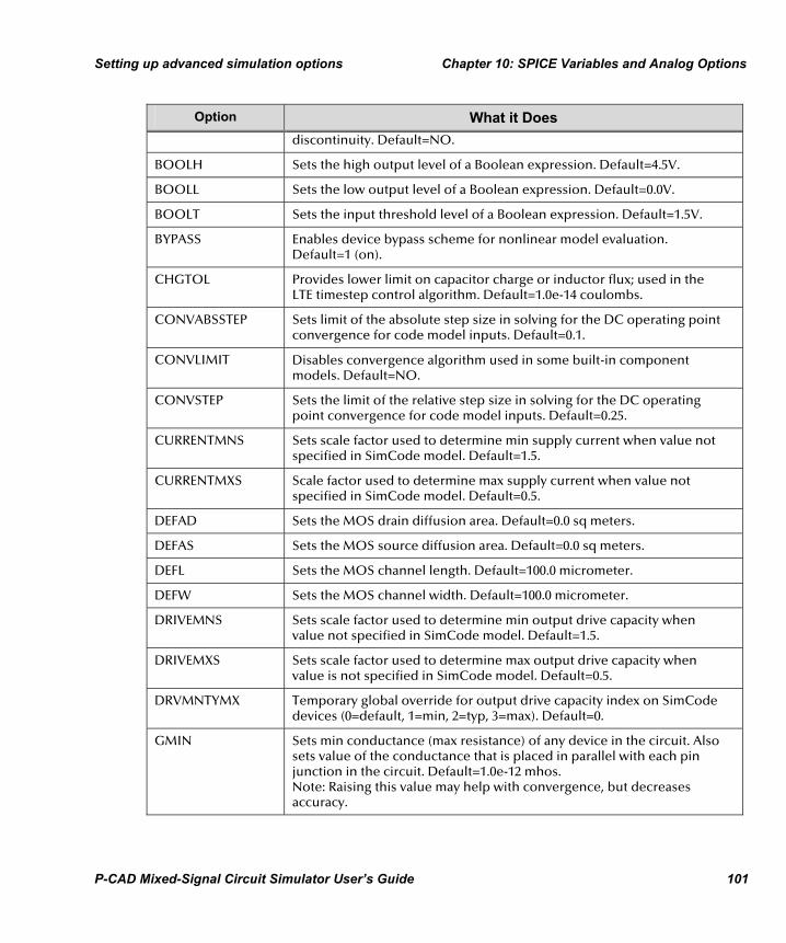
Setting up advanced simulation options Chapter 10: SPICE Variables and Analog Options
P-CAD Mixed-Signal Circuit Simulator User’s Guide 101
Option What it Does discontinuity. Default=NO.
BOOLH Sets the high output level of a Boolean expression. Default=4.5V.
BOOLL Sets the low output level of a Boolean expression. Default=0.0V.
BOOLT Sets the input threshold level of a Boolean expression. Default=1.5V.
BYPASS Enables device bypass scheme for nonlinear model evaluation. Default=1 (on).
CHGTOL Provides lower limit on capacitor charge or inductor flux; used in the LTE timestep control algorithm. Default=1.0e-14 coulombs.
CONVABSSTEP Sets limit of the absolute step size in solving for the DC operating point convergence for code model inputs. Default=0.1.
CONVLIMIT Disables convergence algorithm used in some built-in component models. Default=NO.
CONVSTEP Sets the limit of the relative step size in solving for the DC operating point convergence for code model inputs. Default=0.25.
CURRENTMNS Sets scale factor used to determine min supply current when value not specified in SimCode model. Default=1.5.
CURRENTMXS Scale factor used to determine max supply current when value not specified in SimCode model. Default=0.5.
DEFAD Sets the MOS drain diffusion area. Default=0.0 sq meters.
DEFAS Sets the MOS source diffusion area. Default=0.0 sq meters.
DEFL Sets the MOS channel length. Default=100.0 micrometer.
DEFW Sets the MOS channel width. Default=100.0 micrometer.
DRIVEMNS Sets scale factor used to determine min output drive capacity when value not specified in SimCode model. Default=1.5.
DRIVEMXS Sets scale factor used to determine max output drive capacity when value is not specified in SimCode model. Default=0.5.
DRVMNTYMX Temporary global override for output drive capacity index on SimCode devices (0=default, 1=min, 2=typ, 3=max). Default=0.
GMIN Sets min conductance (max resistance) of any device in the circuit. Also sets value of the conductance that is placed in parallel with each pin junction in the circuit. Default=1.0e-12 mhos. Note: Raising this value may help with convergence, but decreases accuracy.
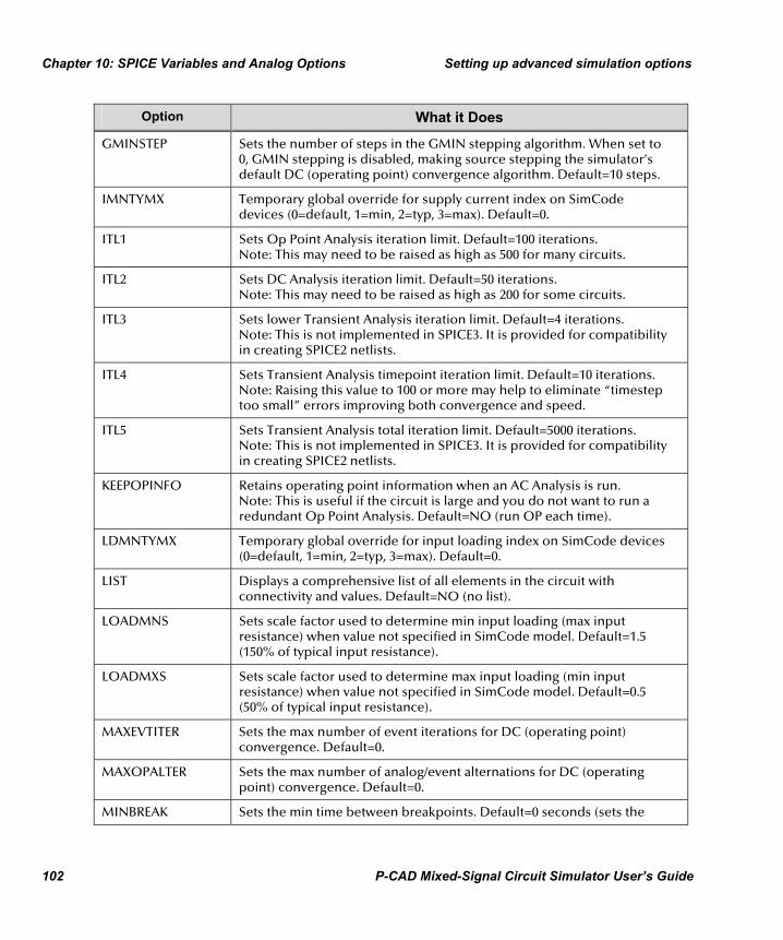
Chapter 10: SPICE Variables and Analog Options Setting up advanced simulation options
102 P-CAD Mixed-Signal Circuit Simulator User’s Guide
Option What it Does GMINSTEP Sets the number of steps in the GMIN stepping algorithm. When set to
0, GMIN stepping is disabled, making source stepping the simulator’s default DC (operating point) convergence algorithm. Default=10 steps.
IMNTYMX Temporary global override for supply current index on SimCode devices (0=default, 1=min, 2=typ, 3=max). Default=0.
ITL1 Sets Op Point Analysis iteration limit. Default=100 iterations. Note: This may need to be raised as high as 500 for many circuits.
ITL2 Sets DC Analysis iteration limit. Default=50 iterations. Note: This may need to be raised as high as 200 for some circuits.
ITL3 Sets lower Transient Analysis iteration limit. Default=4 iterations. Note: This is not implemented in SPICE3. It is provided for compatibility in creating SPICE2 netlists.
ITL4 Sets Transient Analysis timepoint iteration limit. Default=10 iterations. Note: Raising this value to 100 or more may help to eliminate “timestep too small” errors improving both convergence and speed.
ITL5 Sets Transient Analysis total iteration limit. Default=5000 iterations. Note: This is not implemented in SPICE3. It is provided for compatibility in creating SPICE2 netlists.
KEEPOPINFO Retains operating point information when an AC Analysis is run. Note: This is useful if the circuit is large and you do not want to run a redundant Op Point Analysis. Default=NO (run OP each time).
LDMNTYMX Temporary global override for input loading index on SimCode devices (0=default, 1=min, 2=typ, 3=max). Default=0.
LIST Displays a comprehensive list of all elements in the circuit with connectivity and values. Default=NO (no list).
LOADMNS Sets scale factor used to determine min input loading (max input resistance) when value not specified in SimCode model. Default=1.5 (150% of typical input resistance).
LOADMXS Sets scale factor used to determine max input loading (min input resistance) when value not specified in SimCode model. Default=0.5 (50% of typical input resistance).
MAXEVTITER Sets the max number of event iterations for DC (operating point) convergence. Default=0.
MAXOPALTER Sets the max number of analog/event alternations for DC (operating point) convergence. Default=0.
MINBREAK Sets the min time between breakpoints. Default=0 seconds (sets the

Setting up advanced simulation options Chapter 10: SPICE Variables and Analog Options
P-CAD Mixed-Signal Circuit Simulator User’s Guide 103
Option What it Does time automatically).
NOOPALTER Enables DC (operating point) alternations. Default=NO.
NOOPITER Skip directly to GMIN stepping algorithm. Default=NO (don’t skip).
OPTS Displays a list of all standard SPICE3 Option parameter settings. Default=NO (no list).
PIVREL Sets relative ratio between the largest column entry in the matrix and an acceptable pivot value. The value must be between 0 and 1. Default=1.0e-3. In the numerical pivoting algorithm the allowed min pivot is determined by EPSREL=AMAX1(PIVREL*MAXVAL, PIVTOL) where MAXVAL is the max element in the column where a pivot is sought (partial pivoting).
PIVTOL Sets the absolute min value for a matrix entry to be accepted as a pivot. Default=1.0e-13.
PROPMNS Sets scale factor used to determine min propagation delay when value is not specified in SimCode model. Default=0.5 (50% of typical propagation delay).
PROPMXS Sets scale factor used to determine max. propagation delay when value is not specified in SimCode model. Default=1.5 (150% of typical propagation delay).
RAMPTIME Controls turn-on time of independent sources and capacitor and inductor initial conditions from zero to their final value during the time period specified. Default=0.0 seconds.
RELTOL Sets relative error tolerance of the program. The value must be between 0 and 1. Default is 0.001 (0.1%). Larger values mean faster simulation time, but less accuracy.
RSHUNT Value in ohms of resistors added between each circuit node and ground, helping to eliminate problems such as “singular matrix” errors. In general, the value of RSHUNT should be set to a very high resistance (1e+12). Default=0 (no shunt resistors).
SIMWARN A nonzero value allows SimCode warning messages to be displayed at run time. SimCode warnings may include information concerning timing violations (tsetup, thold, etc.) or indicate supply voltage dropping below device specifications. Default=0.
SRCSTEP Sets the number of steps in the source stepping algorithm for DC (operating point) convergence. Default=10 steps.
TEMP Sets the actual operating temperature of the circuit. Any deviation from TNOM will produce a change in the simulation results. Default=27°C.
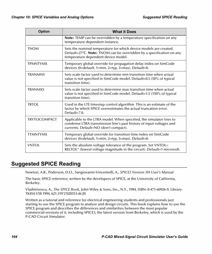
Chapter 10: SPICE Variables and Analog Options Suggested SPICE Reading
104 P-CAD Mixed-Signal Circuit Simulator User’s Guide
Option What it Does Note: TEMP can be overridden by a temperature specification on any temperature dependent instance.
TNOM Sets the nominal temperature for which device models are created. Default=27°C. Note: TNOM can be overridden by a specification on any temperature dependent device model.
TPMNTYMX Temporary global override for propagation delay index on SimCode devices (0=default, 1=min, 2=typ, 3=max). Default=0.
TRANMNS Sets scale factor used to determine min transition time when actual value is not specified in SimCode model. Default=0.5 (50% of typical transition time).
TRANMXS Sets scale factor used to determine max transition time when actual value is not specified in SimCode model. Default=1.5 (150% of typical transition time).
TRTOL Used in the LTE timestep control algorithm. This is an estimate of the factor by which SPICE overestimates the actual truncation error. Default=7.0.
TRYTOCOMPACT Applicable to the LTRA model. When specified, the simulator tries to condense LTRA transmission line’s past history of input voltages and currents. Default=NO (don’t compact).
TTMNTYMX Temporary global override for transition time index on SimCode devices (0=default, 1=min, 2=typ, 3=max). Default=0.
VNTOL Sets the absolute voltage tolerance of the program. Set VNTOL= RELTOL* (lowest voltage magnitude in the circuit). Default=1 microvolt.
Suggested SPICE Reading Newton, A.R., Pederson, D.O., Sangiovanni-Vincentelli, A., SPICE3 Version 3f4 User’s Manual
The basic SPICE reference, written by the developers of SPICE, at the University of California, Berkeley.
Vladimirescu, A., The SPICE Book, John Wiley & Sons, Inc., N.Y., 1994, ISBN: 0-471-60926-9, Library: TK454.V58 1994, 621.319'2'028553-dc20
Written as a tutorial and reference for electrical engineering students and professionals just starting to use the SPICE program to analyze and design circuits. This book explains how to use the SPICE program and describes the differences and similarities between the most popular commercial versions of it, including SPICE3, the latest version from Berkeley, which is used by the P-CAD Circuit Simulator.

Suggested SPICE Reading Chapter 10: SPICE Variables and Analog Options
P-CAD Mixed-Signal Circuit Simulator User’s Guide 105
Kielkowski, R., Inside SPICE, McGraw-Hill, Inc., N.Y., 1994, ISBN: 0-070911525, Library: TK 454.K48 1994, 621.319'2'011353-dc20
Written as a tutorial and reference for electrical engineering students and professionals who are familiar with the SPICE program. This book goes beyond the basics and covers the internal operation of the SPICE program to give the reader a solid understanding of how SPICE works. It provides step-by-step coverage of how to overcome non-convergence, numerical integration instabilities and timestep control errors. It also shows how to make simulations run faster and more efficiently by setting the .OPTION parameters.

P-CAD Mixed-Signal Circuit Simulator User’s Guide 107
CHAPTER 11
Simulating Digital Designs
Due to the complexity of digital devices, it is generally not practical to simulate them using standard, non-event-driven, SPICE instructions. For this reason, Design Explorer's simulation engine includes a special descriptive language called Digital SimCode that allows digital devices to be simulated using an extended version of the event-driven XSPICE. The simulation-ready digital devices included in the P-CAD 2002 schematic libraries all reference Digital SimCode models.
Digital SimCode is a language created specifically for use with the Mixed-Signal Circuit Simulator, and devices created with it are not compatible with other simulators, nor are digital components created for other simulators compatible with the Mixed-Signal Circuit Simulator.
Creating a simulation-ready digital component is similar to creating any simulation-ready component, and you should familiarize yourself with the Creating your own simulation-ready components chapter before attempting to create digital simulation components.
The main difference with digital components for simulation is that:
• digital devices include hidden power and ground power pins in each schematic symbol (VCC or VDD, and GND), and these pins are automatically connected during netlisting. The simulator uses these net names by default, so for a digital-only design it is not necessary to include sources to power these components. By default, VCC = 5V and VDD = 15V.
• digital devices reference an intermediate model (.MDL file) that simply calls the Digital SimCode device description.
Creating new SimCode devices SimCode is a “C like” description language. You use it to define the characteristics and behavior of the device you are modeling. It includes functions to define parameters such as propagation delays, load characteristics, strengths, and so on. The device behavior is defined using truth tables, math functions and conditional control statements, such as IF..THEN. Refer to the SimCode Language Definition topic later in this chapter for a summary of all the language items, and the SimCode Language Syntax topic for complete details of each language item.
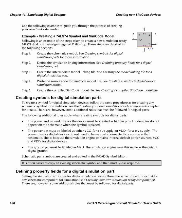
Chapter 11: Simulating Digital Designs Creating new SimCode devices
108 P-CAD Mixed-Signal Circuit Simulator User’s Guide
Use the following example to guide you through the process of creating your own SimCode model.
Example - Creating a 74LS74 Symbol and SimCode Model Following is an example of the steps taken to create a new simulation-ready 74LS74 dual positive-edge triggered D flip-flop. These steps are detailed in the following sections.
Step 1. Create the schematic symbol. See Creating symbols for digital simulation parts for more information.
Step 2. Define the simulation linking information. See Defining property fields for a digital simulation part.
Step 3. Create the intermediate model linking file. See Creating the model linking file for a digital simulation part.
Step 4. Write the source code for SimCode model file. See Creating a SimCode digital device simulation model.
Step 5. Create the compiled SimCode model file. See Creating a compiled SimCode model file.
Creating symbols for digital simulation parts To create a symbol for digital simulation devices, follow the same procedure as for creating any schematic symbol for simulation. See the Creating your own simulation-ready components chapter for details. There are, however, some additional rules that must be followed for digital parts.
The following additional rules apply when creating symbols for digital parts:
• The power and ground pins for the device must be created as hidden pins. Hidden pins do not appear on the schematic when the symbol is placed.
• The power pin must be labeled as either VCC (for a 5V supply) or VDD (for a 15V supply). The power pins for digital devices do not need to be manually connected to a source in the schematic. This is because the simulation engine contains internal default power sources, VCC and VDD, for digital devices.
• The ground pin must be labeled as GND. The simulation engine uses this name as the default digital ground.
Schematic part symbols are created and edited in the P-CAD Symbol Editor.
It is often easier to copy an existing schematic symbol and then modify it as required.
Defining property fields for a digital simulation part Setting the simulation attributes for digital simulation parts follows the same procedure as that for any schematic component for simulation (see Creating your own simulation-ready components). There are, however, some additional rules that must be followed for digital parts.
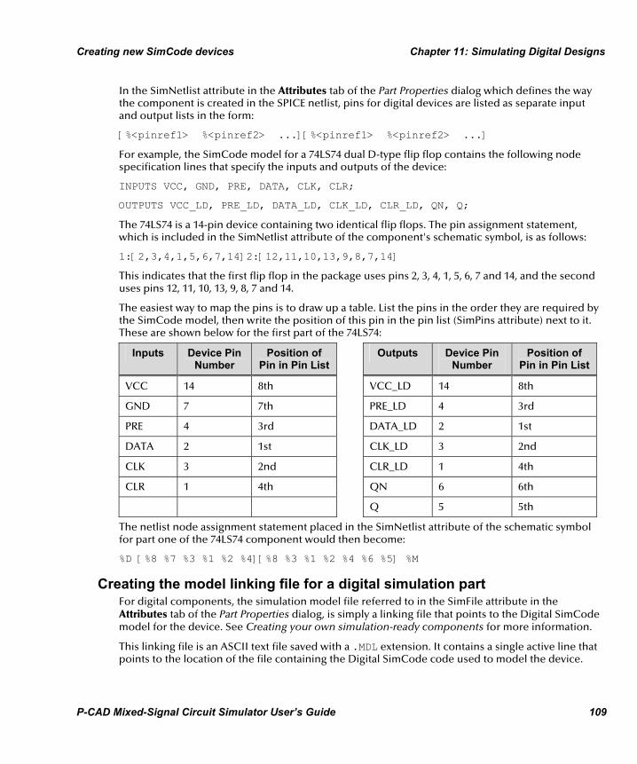
Creating new SimCode devices Chapter 11: Simulating Digital Designs
P-CAD Mixed-Signal Circuit Simulator User’s Guide 109
In the SimNetlist attribute in the Attributes tab of the Part Properties dialog which defines the way the component is created in the SPICE netlist, pins for digital devices are listed as separate input and output lists in the form:
[%<pinref1> %<pinref2> ...][%<pinref1> %<pinref2> ...]
For example, the SimCode model for a 74LS74 dual D-type flip flop contains the following node specification lines that specify the inputs and outputs of the device:
INPUTS VCC, GND, PRE, DATA, CLK, CLR;
OUTPUTS VCC_LD, PRE_LD, DATA_LD, CLK_LD, CLR_LD, QN, Q;
The 74LS74 is a 14-pin device containing two identical flip flops. The pin assignment statement, which is included in the SimNetlist attribute of the component's schematic symbol, is as follows:
1:[2,3,4,1,5,6,7,14]2:[12,11,10,13,9,8,7,14]
This indicates that the first flip flop in the package uses pins 2, 3, 4, 1, 5, 6, 7 and 14, and the second uses pins 12, 11, 10, 13, 9, 8, 7 and 14.
The easiest way to map the pins is to draw up a table. List the pins in the order they are required by the SimCode model, then write the position of this pin in the pin list (SimPins attribute) next to it. These are shown below for the first part of the 74LS74:
Inputs Device Pin Number
Position of Pin in Pin List
Outputs Device Pin Number
Position of Pin in Pin List
VCC 14 8th VCC_LD 14 8th
GND 7 7th PRE_LD 4 3rd
PRE 4 3rd DATA_LD 2 1st
DATA 2 1st CLK_LD 3 2nd
CLK 3 2nd CLR_LD 1 4th
CLR 1 4th QN 6 6th
Q 5 5th
The netlist node assignment statement placed in the SimNetlist attribute of the schematic symbol for part one of the 74LS74 component would then become:
%D [%8 %7 %3 %1 %2 %4][%8 %3 %1 %2 %4 %6 %5] %M
Creating the model linking file for a digital simulation part For digital components, the simulation model file referred to in the SimFile attribute in the Attributes tab of the Part Properties dialog, is simply a linking file that points to the Digital SimCode model for the device. See Creating your own simulation-ready components for more information.
This linking file is an ASCII text file saved with a .MDL extension. It contains a single active line that points to the location of the file containing the Digital SimCode code used to model the device.

Chapter 11: Simulating Digital Designs Creating new SimCode devices
110 P-CAD Mixed-Signal Circuit Simulator User’s Guide
The syntax of this model reference line is:
.MODEL <model_name> XSIMCODE(file="<model_file>"
func=<function_name> [data="<data_file>"] {mntymx})
where:
<model_name> Model name. This must be the same as the name specified in the SimModel attribute in the Attributes tab of the Part Properties dialog. If the <parttype> statement is used, the model name is the same as the device name in the Type field in the Symbol tab of the Part Properties dialog.
<model_file> Name and path of the file containing the device’s digital SimCode model.
<function_name> Specifies the device’s digital SimCode function name. SimCode model files can contain descriptions of more than one device, each identified by a function name in the SimCode.
<data_file> Optional. Name and path of a file containing ASCII data. This file is used by the READ_DATA SimCode function.
Note: The {mntymx} expression at the end of the .MODEL statement is used internally by the simulation engine to indicate that the parameters are for use with Digital SimCode. This must appear exactly as shown.
Example
The following example is from the SN74LS74.MDL file referenced by the SN74LS74AD device in the TI Logic Flip-Flop.Lib library.
.MODEL SN74LS74 xsimcode(file="{MODEL_PATH}LS.SCB" func=ls74 {mntymx})
This model statement tells the simulator to use the LS74 function within the LS.SCB SimCode model file, which is found in the default model path. {MODEL_PATH} is a shortcut to the Models directory specified in the AdvSim99SE.INI file.
A .SCB file contains the compiled code model(s). It is possible to use the initial Digital SimCode source .TXT file for simulation. The model code will be automatically compiled when the simulation is run and the compiled code will be available in the resulting Simlist.TXT file. Use the search facility of Windows Explorer to locate this file, if necessary. A .SCB file could then be created using the compiled code section as content.
If a source code model .TXT file is used, the .MODEL statement in the .MDL file will need to point to this .TXT file instead of a .SCB file. Using the previous example and assuming that the initial source code might have been written in a file called LS74.TXT, the .MODEL statement would now become:
.MODEL SN74LS74 xsimcode(file="{MODEL_PATH}LS74.TXT" func=ls74 {mntymx})
Creating new SimCode devices Chapter 11: Simulating Digital Designs
P-CAD Mixed-Signal Circuit Simulator User’s Guide 111
Creating a SimCode digital device simulation model For a digital part to be simulated, its behavior must be described by a Digital SimCode function contained in a SimCode model file. The SimCode function is called by a .MODEL statement contained in a .MDL file, which is referenced in the SimModel attribute in the Attributes tab of the Properties dialog for the part. See the Creating your own simulation-ready components chapter for more information.
Digital SimCode files are initially written as ASCII text files. SimCode files can be created using any text editor, including the in-built Design Explorer 99 SE text editor. The file can be given any name and extension, as long as it matches the file name listed in the “file=” parameter in the .MDL file. Typically it is named the same as the device, 74LS74.TXT for this example. Multiple digital SimCode device models can be placed in the same file, each is referenced by the “func=” parameter. Refer to the SimCode language Reference section below for complete details of each language item.
A single SimCode file can contain descriptions of a number of digital devices. Each device description within the model file begins with the # xxxx source SimCode definition function and ends with an EXIT function. The statements between these two lines define the behavior of the device in SimCode.
There is an example of the SimCode for a 74LS74 later in this chapter. This SimCode can be copied and pasted directly from the On-line help file if you do not want to type it in.
Test the new device by creating a simple circuit to test its functionality. It is advisable to only test one new device at a time.
When you run the simulation, the source code model is automatically compiled and written to an ASCII text file called Simlist.TXT. Use the search facility of Windows Explorer to locate this file. This file also contains a listing of the execution order of the source code model. Refine the SimCode source model as needed, and continue testing until you have completely debugged the model.
Creating a compiled SimCode model file Once the SimCode has been successfully compiled, you can extract the compiled model information from the Simlist.TXT file, and create a compiled model file (74LS74.SCB for this example). Again you can store multiple models in a single file, but you must set the file= parameter in the .MDL file to be the same as the file name of the compiled SimCode model library.
For a full SimCode example listing of a 74LS74 Dual D-type flip flop, see the SimCode digital simulation model example below.
SimCode digital simulation model example Following is a description of each section of a SimCode file describing a 74LS74 device. The SimCode listing for a 74LS74 D flip-flop follows this description.
Section 1 - SimCode Function Identification - # ls74 source identifies the beginning of the SimCode source function for the 74LS74.

Chapter 11: Simulating Digital Designs Creating new SimCode devices
112 P-CAD Mixed-Signal Circuit Simulator User’s Guide
Section 2 - Data declarations - The INPUTS statement declares the names of the input pins. VCC and GND pins are included in this statement. The order of these pins must match the order of their corresponding pin declarations in the SimNetlist attribute in the Attributes tab of the Part Properties dialog.
The OUTPUTS statement declares the names of the output pins. Notice that the input pins are listed here as well, but with the suffix “_LD”. Input pins must also be declared as outputs so that the device can provide a load back on the driving circuitry. VCC pins are included in this statement, but not GND pins. The order of these pins must match the order of their corresponding pin declarations in the SimNetlist attribute in the Attributes tab of the Part Properties dialog.
The PWR_GND_PINS statement declares which pins will be used for device power and ground and samples their voltage levels for later use in the SimCode.
Section 3 - SimCode Function Initialization - The IF (init_sim) THEN section is executed only once, at the beginning of the simulation. In this section we set the device characteristics that are not subject to change due to outside influences, such as databook specifications. The outputs states should also be initialized here to their “most likely” state. The EXIT command should be placed at the end of this section.
Section 4 - LOAD and DRIVE Statements - These statements are used to declare the load and drive capabilities of the device pins.
Section 5 - Device Functionality - This section can vary dramatically from part to part. In this example an EXT_TABLE command has been used. Other device models use a variety of IF...THEN, STATE_BIT, NUMBER, and other statements to define the logical function of the device.
Section 6 - Tests for Device Setup Violations - These tests warn of device setup violations which, in the real world, may cause a device not to function properly. In the simulation, the device will generally still function, but warnings, if enabled, will be displayed.
Section 7 - Output Delays/Post Events - The DELAY statements occur at the end of the SimCode function. These statements actually post the events to the simulation engine to let it know that something has changed, and when these events are scheduled to occur relative to the rest of the simulation. Timing (propagation delay) is assigned to each output based on the databook specifications, input stimulus and the functionality of the device.
The following is the SimCode listing for a 74LS74 D flip-flop described above: //============================================================ Section 1 - SimCode Function Identification # ls74 source //1/2- 74LS74 D flip-flop Digital Simcode Model //typical prop delay values from TI 1981 2nd edition data book //============================================================ #// Section 2 - Data declarations INPUTS VCC, GND, PRE, DATA, CLK, CLR; OUTPUTS VCC_LD, PRE_LD, DATA_LD, CLK_LD, CLR_LD, QN, Q; INTEGERS tblIndex;REALS tplh_val, tphl_val, ts_val, th_val, trec_val, tt_val, temp_tp,
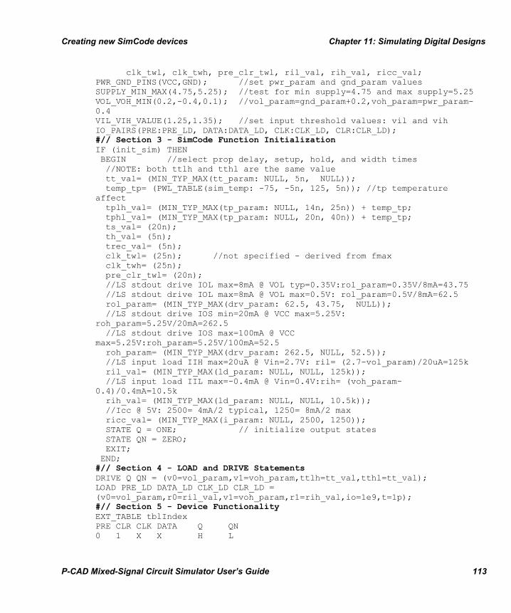
Creating new SimCode devices Chapter 11: Simulating Digital Designs
P-CAD Mixed-Signal Circuit Simulator User’s Guide 113
clk_twl, clk_twh, pre_clr_twl, ril_val, rih_val, ricc_val; PWR_GND_PINS(VCC,GND); //set pwr_param and gnd_param values SUPPLY_MIN_MAX(4.75,5.25); //test for min supply=4.75 and max supply=5.25 VOL_VOH_MIN(0.2,-0.4,0.1); //vol_param=gnd_param+0.2,voh_param=pwr_param-0.4 VIL_VIH_VALUE(1.25,1.35); //set input threshold values: vil and vih IO_PAIRS(PRE:PRE_LD, DATA:DATA_LD, CLK:CLK_LD, CLR:CLR_LD); #// Section 3 - SimCode Function Initialization IF (init_sim) THEN BEGIN //select prop delay, setup, hold, and width times //NOTE: both ttlh and tthl are the same value tt_val= (MIN_TYP_MAX(tt_param: NULL, 5n, NULL)); temp_tp= (PWL_TABLE(sim_temp: -75, -5n, 125, 5n)); //tp temperature affect tplh_val= (MIN_TYP_MAX(tp_param: NULL, 14n, 25n)) + temp_tp; tphl_val= (MIN_TYP_MAX(tp_param: NULL, 20n, 40n)) + temp_tp; ts_val= (20n); th_val= (5n); trec_val= (5n); clk_twl= (25n); //not specified - derived from fmax clk_twh= (25n); pre_clr_twl= (20n); //LS stdout drive IOL max=8mA @ VOL typ=0.35V:rol_param=0.35V/8mA=43.75 //LS stdout drive IOL max=8mA @ VOL max=0.5V: rol_param=0.5V/8mA=62.5 rol_param= (MIN_TYP_MAX(drv_param: 62.5, 43.75, NULL)); //LS stdout drive IOS min=20mA @ VCC max=5.25V: roh_param=5.25V/20mA=262.5 //LS stdout drive IOS max=100mA @ VCC max=5.25V:roh_param=5.25V/100mA=52.5 roh_param= (MIN_TYP_MAX(drv_param: 262.5, NULL, 52.5)); //LS input load IIH max=20uA @ Vin=2.7V: ril= (2.7-vol_param)/20uA=125k ril_val= (MIN_TYP_MAX(ld_param: NULL, NULL, 125k)); //LS input load IIL max=-0.4mA @ Vin=0.4V:rih= (voh_param-0.4)/0.4mA=10.5k rih_val= (MIN_TYP_MAX(ld_param: NULL, NULL, 10.5k)); //Icc @ 5V: 2500= 4mA/2 typical, 1250= 8mA/2 max ricc_val= (MIN_TYP_MAX(i_param: NULL, 2500, 1250)); STATE Q = ONE; // initialize output states STATE QN = ZERO; EXIT; END; #// Section 4 - LOAD and DRIVE Statements DRIVE Q QN = (v0=vol_param,v1=voh_param,ttlh=tt_val,tthl=tt_val); LOAD PRE_LD DATA_LD CLK_LD CLR_LD = (v0=vol_param,r0=ril_val,v1=voh_param,r1=rih_val,io=1e9,t=1p); #// Section 5 - Device Functionality EXT_TABLE tblIndex PRE CLR CLK DATA Q QN 0 1 X X H L

Chapter 11: Simulating Digital Designs SimCode Language Reference
114 P-CAD Mixed-Signal Circuit Simulator User’s Guide
1 0 X X L H 0 0 X X H H 1 1 ^ X DATA ~DATA 1 1 X X Q ~Q; LOAD VCC_LD = (v0=gnd_param,r0=ricc_val,t=1p); #// Section 6 - Tests for Device Setup Violations IF (warn_param) THEN BEGIN IF (PRE && CLR) THEN BEGIN SETUP_HOLD(CLK=LH DATA Ts=ts_val Th=th_val "CLK->DATA"); RECOVER(CLK=LH PRE CLR Trec=trec_val "CLK->PRE or CLR"); WIDTH(CLK Twl=clk_twl Twh=clk_twh "CLK"); WIDTH(PRE CLR Twl= pre_clr_twl "PRE or CLR"); END; END; #// Section 7 - Output Delays/Post Events DELAY Q QN = CASE (TRAN_LH) : tplh_val CASE (TRAN_HL) : tphl_val END; EXIT;
SimCode Language Reference SimCode is a “C like” description language used to define the characteristics and behavior of the device you are modeling. SimCode files are written as plain ASCII text files and saved with the .TXT extension.
SimCode statement termination character The SimCode language uses the semicolon character " ; " to mark the end of SimCode statement.
In SimCode, a statement may occupy a single line of code, or take up several lines. The termination character marks the termination of the complete SimCode statement and is placed immediately after the last clause of the statement, as shown in the following examples:
DELAY Q1 Q2 Q3 Q4 = 10n; DELAY Q QN = CASE (TRAN_LH) : tplh_val CASE (TRAN_HL) : tphl_val END; data = (E0_1 && (CHANGED(D0) || CHANGED(D1))); DELAY Q1 Q0 =

SimCode Language Definition Chapter 11: Simulating Digital Designs
P-CAD Mixed-Signal Circuit Simulator User’s Guide 115
CASE (data && TRAN_LH) : tplh_D_Q CASE (data && TRAN_HL) : tphl_D_Q CASE (TRAN_LH) : tplh_E_Q CASE (TRAN_HL) : tphl_E_Q END;
Beginning a SimCode model definition A SimCode device definition begins with a # xxxx source statement. This statement has the form:
# <func name> source
where <func name> is the name of the simulation function used to identify the model definition block. The model definition block ends with the EXIT statement. Therefore, a SimCode model for a particular device takes the general form:
# MyDevice source ... ... ... EXIT;
In the above code fragment, the .MODEL statement contained in the .MDL file referenced by the schematic part symbol would call the function MyDevice in order to simulate the device.
A single SimCode text file can contain any number of model definitions.
Including comments in SimCode files You may include comments in a SimCode file by preceding the comments with two "slash" characters //. Everything after the slash characters is ignored. Comments can appear as complete lines, or after a SimCode line, as shown in the following examples:
EVENT = (present_time + 1e-6); //return in 1us DELAY Q QN = // Case 1 CASE (TRAN_LH) : tplh_val // Case 2 CASE (TRAN_HL) : tphl_val END;
Comments should be placed in SimCode models to make the code more readable and to aid in debugging.
SimCode Language Definition The following items make up the Digital SimCode language. The following pages describe each of these items in detail.
INPUTS Input pins (pins that monitor the circuit)
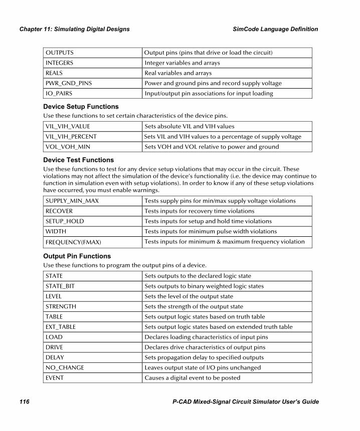
Chapter 11: Simulating Digital Designs SimCode Language Definition
116 P-CAD Mixed-Signal Circuit Simulator User’s Guide
OUTPUTS Output pins (pins that drive or load the circuit)
INTEGERS Integer variables and arrays
REALS Real variables and arrays
PWR_GND_PINS Power and ground pins and record supply voltage
IO_PAIRS Input/output pin associations for input loading
Device Setup Functions Use these functions to set certain characteristics of the device pins.
VIL_VIH_VALUE Sets absolute VIL and VIH values
VIL_VIH_PERCENT Sets VIL and VIH values to a percentage of supply voltage
VOL_VOH_MIN Sets VOH and VOL relative to power and ground
Device Test Functions Use these functions to test for any device setup violations that may occur in the circuit. These violations may not affect the simulation of the device’s functionality (i.e. the device may continue to function in simulation even with setup violations). In order to know if any of these setup violations have occurred, you must enable warnings.
SUPPLY_MIN_MAX Tests supply pins for min/max supply voltage violations
RECOVER Tests inputs for recovery time violations
SETUP_HOLD Tests inputs for setup and hold time violations
WIDTH Tests inputs for minimum pulse width violations
FREQUENCY(FMAX) Tests inputs for minimum & maximum frequency violation
Output Pin Functions Use these functions to program the output pins of a device.
STATE Sets outputs to the declared logic state
STATE_BIT Sets outputs to binary weighted logic states
LEVEL Sets the level of the output state
STRENGTH Sets the strength of the output state
TABLE Sets output logic states based on truth table
EXT_TABLE Sets output logic states based on extended truth table
LOAD Declares loading characteristics of input pins
DRIVE Declares drive characteristics of output pins
DELAY Sets propagation delay to specified outputs
NO_CHANGE Leaves output state of I/O pins unchanged
EVENT Causes a digital event to be posted
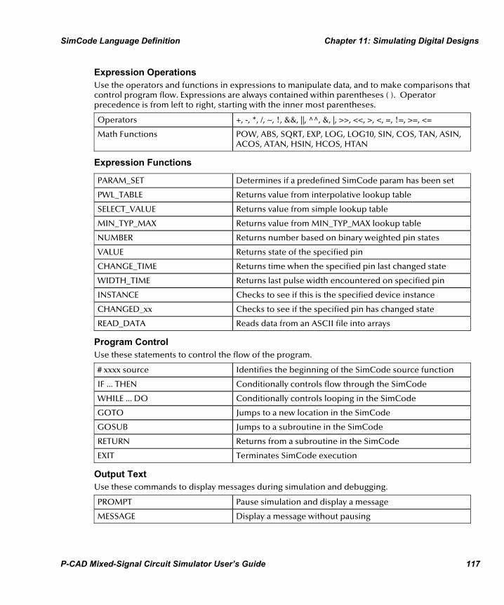
SimCode Language Definition Chapter 11: Simulating Digital Designs
P-CAD Mixed-Signal Circuit Simulator User’s Guide 117
Expression Operations Use the operators and functions in expressions to manipulate data, and to make comparisons that control program flow. Expressions are always contained within parentheses ( ). Operator precedence is from left to right, starting with the inner most parentheses.
Operators +, -, *, /, ~, !, &&, ||, ^^, &, |, >>, <<, >, <, =, !=, >=, <=
Math Functions POW, ABS, SQRT, EXP, LOG, LOG10, SIN, COS, TAN, ASIN, ACOS, ATAN, HSIN, HCOS, HTAN
Expression Functions
PARAM_SET Determines if a predefined SimCode param has been set
PWL_TABLE Returns value from interpolative lookup table
SELECT_VALUE Returns value from simple lookup table
MIN_TYP_MAX Returns value from MIN_TYP_MAX lookup table
NUMBER Returns number based on binary weighted pin states
VALUE Returns state of the specified pin
CHANGE_TIME Returns time when the specified pin last changed state
WIDTH_TIME Returns last pulse width encountered on specified pin
INSTANCE Checks to see if this is the specified device instance
CHANGED_xx Checks to see if the specified pin has changed state
READ_DATA Reads data from an ASCII file into arrays
Program Control Use these statements to control the flow of the program.
# xxxx source Identifies the beginning of the SimCode source function
IF ... THEN Conditionally controls flow through the SimCode
WHILE ... DO Conditionally controls looping in the SimCode
GOTO Jumps to a new location in the SimCode
GOSUB Jumps to a subroutine in the SimCode
RETURN Returns from a subroutine in the SimCode
EXIT Terminates SimCode execution
Output Text Use these commands to display messages during simulation and debugging.
PROMPT Pause simulation and display a message
MESSAGE Display a message without pausing
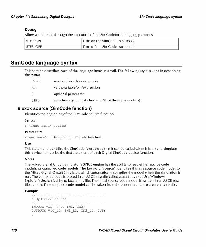
Chapter 11: Simulating Digital Designs SimCode language syntax
118 P-CAD Mixed-Signal Circuit Simulator User’s Guide
Debug Allow you to trace through the execution of the SimCodefor debugging purposes.
STEP_ON Turn on the SimCode trace mode
STEP_OFF Turn off the SimCode trace mode
SimCode language syntax This section describes each of the language items in detail. The following style is used in describing the syntax:
italics reserved words or emphasis
< > value/variable/pin/expression
[ ] optional parameter
{ }|{ } selections (you must choose ONE of these parameters).
# xxxx source (SimCode function) Identifies the beginning of the SimCode source function.
Syntax # <func name> source
Parameters
<func name> Name of the SimCode function.
Use
This statement identifies the SimCode function so that it can be called when it is time to simulate this device. It must be the first statement of each Digital SimCode device function.
Notes
The Mixed-Signal Circuit Simulator’s SPICE engine has the ability to read either source code models, or compiled code models. The keyword “source” identifies this as a source code model to the Mixed-Signal Circuit Simulator, which automatically compiles the model when the simulation is run. The compiled code is placed in an ASCII text file called Simlist.TXT. Use Windows Explorer’s Search facility to locate this file. The initial source code model is written in an ASCII text file (.TXT). The compiled code model can be taken from the Simlist.TXT to create a .SCB file.
Example //================================== # MyDevice source //================================== INPUTS VCC, GND, IN1, IN2; OUTPUTS VCC_LD, IN1_LD, IN2_LD, OUT; .

SimCode language syntax Chapter 11: Simulating Digital Designs
P-CAD Mixed-Signal Circuit Simulator User’s Guide 119
.
. EXIT;
CHANGE_TIME (SimCode function) Returns time when the specified pin last changed state.
Syntax CHANGE_TIME(<pin>)
Parameter
<pin> Input or output pin name.
Use
This function returns a real value that indicates the last time the specified input or output pin changed states.
Example T1 = (CHANGE_TIME(INA));
CHANGED_xx (SimCode function) Checks if the specified pin has changed state.
Syntax CHANGED_xx(<pin> [{<}|{<=}|{>}|{>=} <var/time/value>])
Parameters
<pin> Input or output pin name.
<var/time/value> Item to which <pin> is compared.
Use
The CHANGED_xx function is used to determine if the specified <pin> has changed state. The _xx that follows the keyword CHANGED can be eliminated (to indicate any type of change) or the xx can be set to:
LH, LX, HL, HX, XL, XH, LZ, ZL, ZH, ZX, HZ or XZ
to indicate a specific type of change. The optional compare operator (<, <=, >, >=) and <var/time/value> would be included to check for a more specific change. If they are not included, the function will return 1 if the pin has changed at the current simulation step.
Examples IF (CHANGED_LH(CLK)) THEN ... IF (CHANGED(DATA < 10n)) THEN ...

Chapter 11: Simulating Digital Designs SimCode language syntax
120 P-CAD Mixed-Signal Circuit Simulator User’s Guide
DELAY (SimCode function) Sets propagation delay to specified outputs.
Syntax 1 DELAY <output> [<output> ...] = <delay>;
Syntax 2 DELAY <output> [<output> ...] = CASE (<conditional exp>) : <delay> CASE (<conditional exp>) : <delay> [CASE (<conditional exp>) : <delay> ...] END;
Parameters
<output> Name of/variable index to the output pin.
<conditional exp> Conditional expression that determines which delay is used.
<delay> Propagation delay time to the output pin.
Use
The DELAY command is executed once for each pin listed and posts a propagation delay for each pin that has changed its level. The CASE option allows more than one <delay> to be specified. The <conditional exp> then determines which <delay> will be used. If a delay is set for a pin that has not changed then the pin will be flagged as NO-CHANGE and the delay will NOT be posted. The <delay> can be a real constant, a real variable or a real expression.
Notes
The DELAY command must be executed exactly once for each output pin, that is, for each pin declared in the OUTPUTS statement which is NOT listed in the LOAD or NO_CHANGE statements. The order in which the delays are set is based on the order in which these pins are listed in the DELAY command (i.e. first pin listed is set first). Each <conditional exp> is evaluated in the order it is listed until one expression evaluates TRUE. When this occurs, the <delay> value associated with the TRUE expression is posted for the output being set. When using the CASE option, at least one <conditional exp> should evaluate as TRUE for each output pin listed. If no <conditional exp> evaluates to TRUE, the <delay> associated with the last CASE statement is posted.
In addition to the standard expression functions, the following terms apply ONLY to the output pin being set and can be used in the <conditional exp> :
TRAN_LH low-to-high
TRAN_LX low-to-other
TRAN_HL high-to-low
TRAN_HX high-to-other
TRAN_HZ high-to-tristate
TRAN_XL other-to-low
TRAN_XH other-to-high
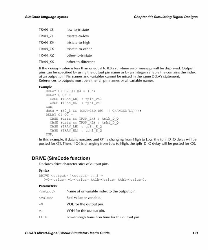
SimCode language syntax Chapter 11: Simulating Digital Designs
P-CAD Mixed-Signal Circuit Simulator User’s Guide 121
TRAN_LZ low-to-tristate
TRAN_ZL tristate-to-low
TRAN_ZH tristate-to-high
TRAN_ZX tristate-to-other
TRAN_XZ other-to-tristate
TRAN_XX other-to-different
If the <delay> value is less than or equal to 0.0 a run-time error message will be displayed. Output pins can be specified by using the output pin name or by an integer variable the contains the index of an output pin. Pin names and variables cannot be mixed in the same DELAY statement. References to outputs must be either all pin names or all variable names.
Example DELAY Q1 Q2 Q3 Q4 = 10n; DELAY Q QN = CASE (TRAN_LH) : tplh_val CASE (TRAN_HL) : tphl_val END; data = (E0_1 && (CHANGED(D0) || CHANGED(D1))); DELAY Q1 Q0 = CASE (data && TRAN_LH) : tplh_D_Q CASE (data && TRAN_HL) : tphl_D_Q CASE (TRAN_LH) : tplh_E_Q CASE (TRAN_HL) : tphl_E_Q END;
In this example, if data is nonzero and Q1 is changing from High to Low, the tphl_D_Q delay will be posted for Q1. Then, if Q0 is changing from Low to High, the tplh_D_Q delay will be posted for Q0.
DRIVE (SimCode function) Declares drive characteristics of output pins.
Syntax DRIVE <output> [<output> ...] = (v0=<value> v1=<value> ttlh=<value> tthl=<value>);
Parameters
<output> Name of or variable index to the output pin.
<value> Real value or variable.
v0 VOL for the output pin.
v1 VOH for the output pin.
ttlh Low-to-high transition time for the output pin.
Chapter 11: Simulating Digital Designs SimCode language syntax
122 P-CAD Mixed-Signal Circuit Simulator User’s Guide
tthl High-to-low transition time for the output pin.
Use
The DRIVE command is used to declare the output pin’s drive characteristics. When the output is set to a LOW state, the output pin is connected to voltage value v0 through resistance rol_param. When the output is set to a HIGH state, the output pin is connected to voltage value v1 through resistance roh_param. The low-to-high transition time is set by ttlh and the high-to-low transition time is set by tthl.
Notes
Pin names and variables cannot be mixed in the same DRIVE statement. References to outputs must be either all pin names or all variable names.
The values used for rol_param should be derived using the databook specs for VOL. This value represents the total saturation resistance of the pull-down structure of the device’s output. A standard LS output in the LOW state, for example, sinking 8mA will not exceed 0.5V, typically closer to 0.35V. Therefore:
for typ LOW state drive: rol_param = VOLtyp / IOLmax
rol_param = 0.35V / 8mA
rol_param = 43.75 ohms
for min LOW state drive: rol_param = VOLmax / IOLmax
rol_param = 0.5V / 8mA
rol_param = 62.5 ohms
The values used for roh_param should be derived using the databook specs for IOS, if available. This value represents the total saturation resistance of the pull-up structure of the device’s output. A standard LS output in the HIGH state with the output shorted to ground and Vcc=5.25V will source at least 20mA but not more than 100mA. Therefore:
for min HIGH state drive: roh_param = VCCmax / IOSmin
roh_param = 5.25V / 20mA
roh_param = 262.5 ohms
for max HIGH state drive: roh_param = VCCmax / IOSmax
roh_param = 5.25V / 100mA
roh_param = 52.5 ohms
Example rol_param = (MIN_TYP_MAX(drv_param: 62.5, 43.75, NULL); roh_param = (MIN_TYP_MAX(drv_param: 262.5, NULL, 52.5); DRIVE Q QN = (v0=vol_param,v1=voh_param,ttlh=ttlh_val, tthl=tthl_val);
SimCode language syntax Chapter 11: Simulating Digital Designs
P-CAD Mixed-Signal Circuit Simulator User’s Guide 123
See Also
LOAD
EVENT (SimCode function) Causes a digital event to be posted.
Syntax EVENT = ({<time>}|{<expression>})
Parameters
<time> Time at which event should occur.
<expression> Expression indicating time at which event should occur.
Use
In most cases, a digital event is posted when one or more INPUT pins for a SimCode model changes state. When the event is processed, the SimCode for the specified event is called and run. This instruction allows a SimCode model to post a digital event at a specified <time>. If the specified EVENT time is greater than the simulation time (indicated by present_time), then a digital event will be posted. If more than one EVENT is posted in a single call to a SimCode model, only the longest EVENT <time> will be used. This function allows the creation of one-shots and other similar device models.
Notes
If a digital event for a specific SimCode model occurs before an EVENT <time> posted by that SimCode, the EVENT <time> must be posted again. For example, if 1) the present simulation time is 1us, 2) a SimCode model sets EVENT = 2us and 3) an INPUT pin in the SimCode model changes state at 1.5us, then the 2us event must be posted again.
Example EVENT = (present_time + 1e-6); //return in 1us
EXIT (SimCode function) Terminates SimCode execution.
Syntax EXIT
Note
This is the last line of a SimCode model, but it may also be placed at other locations to abort execution of remaining SimCode.

Chapter 11: Simulating Digital Designs SimCode language syntax
124 P-CAD Mixed-Signal Circuit Simulator User’s Guide
EXT_TABLE (SimCode function) Sets output logic states based on extended truth table.
Syntax EXT_TABLE <line>
<input pin> [<input pin> ...] <output pin> [<output pin> ...]
<input state> [<input state> ...]
<output state> [<output state> ...];
Parameters
<line> Variable into which the line number used in the table is placed
<input pin> Name of the input pin
<output pin> Name of the output pin
<input state> State of the individual inputs
<output state> State of the individual outputs based on input conditions
Use
The EXT_TABLE statement is an extended truth table function used to set the level and strength of the specified outputs. Valid input states are:
0 low (input voltage is <= vil_param)
1 high (input voltage is >= vih_param)
^ low-to-high-transition
v high-to-low-transition
X don’t care what input voltage is
Valid output states are:
L ZERO (set output level to vol_param).
H ONE (set output level to voh_param).
Z UNKNOWN (set output level to v3s_param).
It also allows INPUT and/or OUTPUT pin names with optional prefixes to specify the output states. Prefixes are:
- State is the previous state.
~ State is the inverse of the state.
-~ State is the inverse of the previous state.
Output state letters can be followed by a colon and a letter to indicate strength:
SimCode language syntax Chapter 11: Simulating Digital Designs
P-CAD Mixed-Signal Circuit Simulator User’s Guide 125
s STRONG (set output to rol_param for L and roh_param for H).
z HI_IMPEDANCE (set output to r3s_param).
If a strength character is not specified after an output state then STRONG will be used for L and H states and HI_IMPEDANCE will be used for Z states.
Notes
Each row is tested sequentially from top to bottom until the input conditions are met. The outputs are set for the first row to meet the input conditions. <line> is set to the line number in the table that was used. If no match was made then <line> is set to 0. Pin names used to specify output states do not need to be in the table heading. Unlike the TABLE statement, input variables are not allowed.
Example EXT_TABLE tblIndex
PRE CLR CLK DATA Q QN 0 1 X X H L 1 0 X X L H 0 0 X X H H 1 1 ^ X DATA ~DATA 1 1 X X Q ~Q;
This example is representative of 1/2 of a 7474 D type flip-flop. If input pins PRE, CLR, and DATA are all high (>= vih_param) and CLK has a low-to-high transition, Q is set to high (voh_param) and STRONG (roh_param), QN is set to low (vol_param) and STRONG (rol_param) and tblIndex is set to 4.
See Also
REALS, STATE, STATE_BIT, TABLE
FREQUENCY (FMAX) (SimCode function) Tests inputs for minimum and maximum frequency violation.
Syntax FREQUENCY(<input> [<input>...] MIN=<frequency> MAX=<frequency> ["<message>"])
Parameters
<input> Name of or variable index to the input pin under test.
MIN Minimum frequency allowed on the pin under test.
MAX Maximum frequency allowed on the pin under test.
<message> Text string that will be displayed if a warning occurs.

Chapter 11: Simulating Digital Designs SimCode language syntax
126 P-CAD Mixed-Signal Circuit Simulator User’s Guide
Use
The FREQUENCY function compares the <input> period (the time from one low-to-high edge to the next low-to-high edge) with the reciprocal of the specified <frequency> (1/freq). If the time period for the <input> is smaller than the reciprocal of the specified MAX<frequency> or the time period for the <input> is greater than the reciprocal of the specified MIN<frequency>, then a WARNING will be displayed. An optional <message> string can be included in the FREQUENCY statement which will be output if a WARNING is displayed.
Notes
Databook specifications should be used with this function. Pin and variable names can be mixed in the same FREQUENCY statement. Only the first FREQUENCY failure for each pin listed will be reported.
Example FREQUENCY(CLK MAX=10MEG "CLK"); //check fmax only
GOSUB (SimCode function) Jumps to a subroutine in the SimCode.
Syntax GOSUB <label>;
Parameters
<label> Location in SimCode where program flow resumes.
Use
The GOSUB instruction is used to perform non-sequential execution of the SimCode. However, unlike the GOTO statement, SimCode execution will continue on the instruction following the GOSUB instruction when a RETURN instruction is encountered in the SimCode being run.
Example
GOSUB Shift_Left; . . Exit; Shift_Left: . . RETURN:
See Also
RETURN
SimCode language syntax Chapter 11: Simulating Digital Designs
P-CAD Mixed-Signal Circuit Simulator User’s Guide 127
GOTO (SimCode function) Jumps to a new location in the SimCode.
Syntax GOTO <label>;
Parameters
<label> Location in SimCode where program flow resumes.
Use
The GOTO instruction is used to perform non-sequential execution of the SimCode.
Notes
Program flow resumes from the location where <label>: appears in the SimCode. <label> must being with an alpha character, followed by any number of alphanumeric characters or the underscore ( _ ) character. Where <label> appears in the code, it must be followed immediately by a colon ( : ).
Example
GOTO Shutdown; . . Shutdown: . . Exit;
See Also
GOSUB, IF ... THEN
IF ... THEN (SimCode function) Conditionally controls flow through the SimCode.
Syntax 1 IF (<expression>) THEN BEGIN ... [ELSE ...] END;
Syntax 2 IF (<expression>) THEN GOTO <label>;
Parameters
<expression> Any expression that can be evaluated as true or false.
<label> Location in SimCode where program flow resumes.
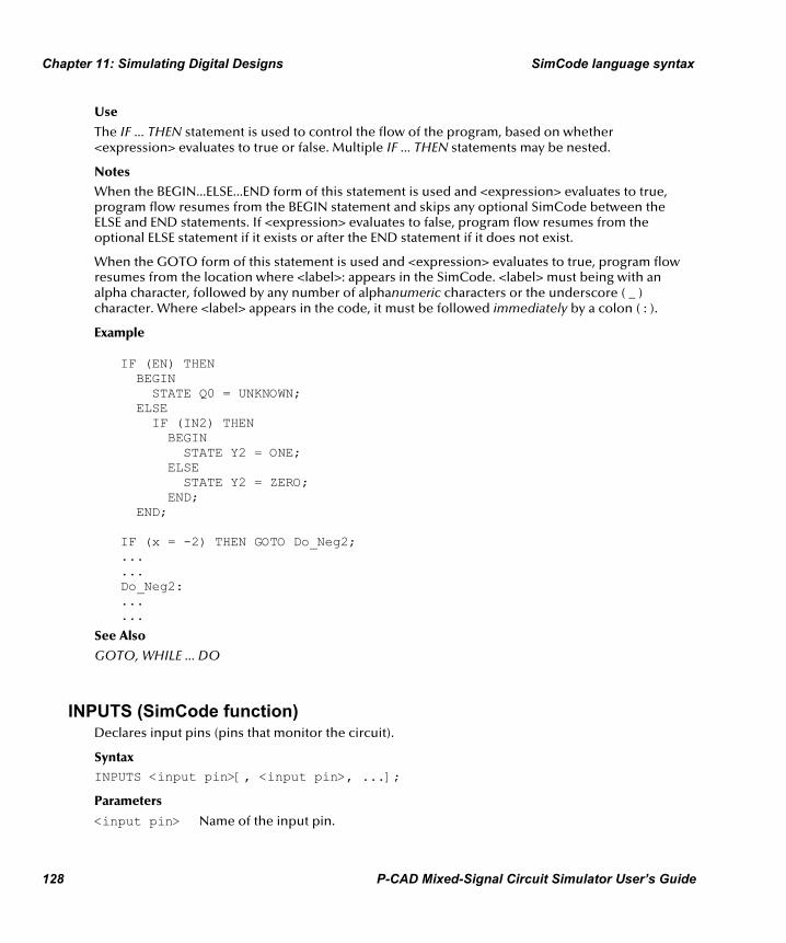
Chapter 11: Simulating Digital Designs SimCode language syntax
128 P-CAD Mixed-Signal Circuit Simulator User’s Guide
Use
The IF ... THEN statement is used to control the flow of the program, based on whether <expression> evaluates to true or false. Multiple IF ... THEN statements may be nested.
Notes
When the BEGIN...ELSE...END form of this statement is used and <expression> evaluates to true, program flow resumes from the BEGIN statement and skips any optional SimCode between the ELSE and END statements. If <expression> evaluates to false, program flow resumes from the optional ELSE statement if it exists or after the END statement if it does not exist.
When the GOTO form of this statement is used and <expression> evaluates to true, program flow resumes from the location where <label>: appears in the SimCode. <label> must being with an alpha character, followed by any number of alphanumeric characters or the underscore ( _ ) character. Where <label> appears in the code, it must be followed immediately by a colon ( : ).
Example
IF (EN) THEN BEGIN STATE Q0 = UNKNOWN; ELSE IF (IN2) THEN BEGIN STATE Y2 = ONE; ELSE STATE Y2 = ZERO; END; END; IF (x = -2) THEN GOTO Do_Neg2; ... ... Do_Neg2: ... ...
See Also
GOTO, WHILE ... DO
INPUTS (SimCode function) Declares input pins (pins that monitor the circuit).
Syntax INPUTS <input pin>[, <input pin>, ...];
Parameters
<input pin> Name of the input pin.
SimCode language syntax Chapter 11: Simulating Digital Designs
P-CAD Mixed-Signal Circuit Simulator User’s Guide 129
Use
The INPUTS data type is used to define the pins which monitor stimulus external to the device. These generally include input, i/o, power and ground pins.
Notes
Input pin names must begin with a letter and be defined before they are used.
Example INPUTS VCC, GND, PRE, DATA, CLK, CLR;
See Also
OUTPUTS, IO_PAIRS, PWR_GND_PINS
INSTANCE (SimCode function) Checks if this is the specified device instance.
Syntax INSTANCE("<instance name>")
Parameters
<instance name> Text string indicating instance name.
Use
The INSTANCE function returns 1 if the present instance of the SimCode device matches the <instance name> specified. Otherwise it returns 0;
Notes
A circuit may contain more than one of any given device. During simulation it may be important to know if the device being simulated at this moment is the one you are interested in. This would allow you, for example, to print messages for one specific NAND gate without having to wade through messages for all the other NAND gates as well. The instance name is the device Designation preceded by its SPICE Prefix Character (the letter A).
Example
IF (INSTANCE("AU23")) THEN BEGIN MESSAGE("U23-Q0 = %d", Q0); END;
INTEGERS (SimCode function) Declares integer variables and arrays.
Syntax INTEGERS <var>[, <var>, ...];
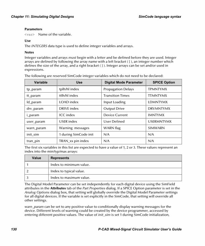
Chapter 11: Simulating Digital Designs SimCode language syntax
130 P-CAD Mixed-Signal Circuit Simulator User’s Guide
Parameters
<var> Name of the variable.
Use
The INTEGERS data type is used to define integer variables and arrays.
Notes
Integer variables and arrays must begin with a letter and be defined before they are used. Integer arrays are defined by following the array name with a left bracket ( [ ), an integer number which defines the size of the array, and a right bracket ( ] ). Integer arrays can be set and/or used in expressions.
The following are reserved SimCode integer variables which do not need to be declared:
Variable Use Digital Mode Parameter SPICE Option
tp_param tplh/hl index Propagation Delays TPMNTYMX
tt_param ttlh/hl index Transition Times TTMNTYMX
ld_param LOAD index Input Loading LDMNTYMX
drv_param DRIVE index Output Drive DRVMNTYMX
i_param ICC index Device Current IMNTYMX
user_param USER index User Defined USERMNTYMX
warn_param Warning messages WARN flag SIMWARN
init_sim 1 during SimCode init N/A N/A
tran_pin TRAN_xx pin index N/A N/A
The first six variables in this list are expected to have a value of 1, 2 or 3. These values represent an index into the min/typ/max arrays:
Value Represents
1 Index to minimum value.
2 Index to typical value.
3 Index to maximum value.
The Digital Model Parameter can be set independently for each digital device using the SimField attributes in the Attributes tab of the Part Properties dialog. If a SPICE Option parameter is set in the Analog Options dialog box, that setting will globally override the Digital Model Parameter settings for all digital devices. If the variable is set explicitly in the SimCode, that setting will override all other settings.
warn_param can be set to any positive value to conditionally display warning messages for the device. Different levels of warning could be created by the device programmer, accessed by entering different positive values. The value of init_sim is set 1 during SimCode initialization,
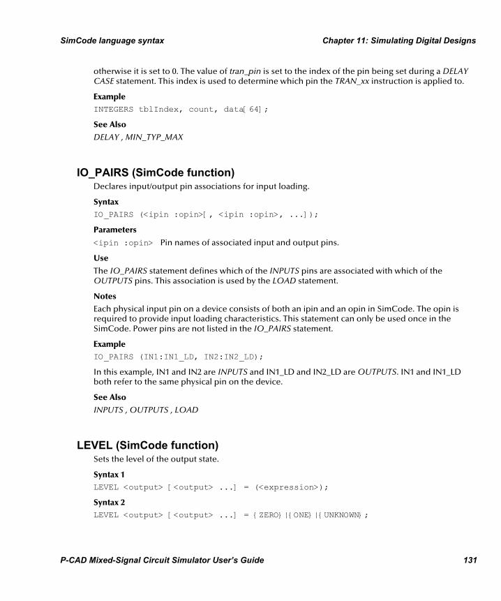
SimCode language syntax Chapter 11: Simulating Digital Designs
P-CAD Mixed-Signal Circuit Simulator User’s Guide 131
otherwise it is set to 0. The value of tran_pin is set to the index of the pin being set during a DELAY CASE statement. This index is used to determine which pin the TRAN_xx instruction is applied to.
Example INTEGERS tblIndex, count, data[64];
See Also
DELAY , MIN_TYP_MAX
IO_PAIRS (SimCode function) Declares input/output pin associations for input loading.
Syntax IO_PAIRS (<ipin :opin>[, <ipin :opin>, ...]);
Parameters
<ipin :opin> Pin names of associated input and output pins.
Use
The IO_PAIRS statement defines which of the INPUTS pins are associated with which of the OUTPUTS pins. This association is used by the LOAD statement.
Notes
Each physical input pin on a device consists of both an ipin and an opin in SimCode. The opin is required to provide input loading characteristics. This statement can only be used once in the SimCode. Power pins are not listed in the IO_PAIRS statement.
Example IO_PAIRS (IN1:IN1_LD, IN2:IN2_LD);
In this example, IN1 and IN2 are INPUTS and IN1_LD and IN2_LD are OUTPUTS. IN1 and IN1_LD both refer to the same physical pin on the device.
See Also
INPUTS , OUTPUTS , LOAD
LEVEL (SimCode function) Sets the level of the output state.
Syntax 1 LEVEL <output> [<output> ...] = (<expression>);
Syntax 2 LEVEL <output> [<output> ...] = {ZERO}|{ONE}|{UNKNOWN};
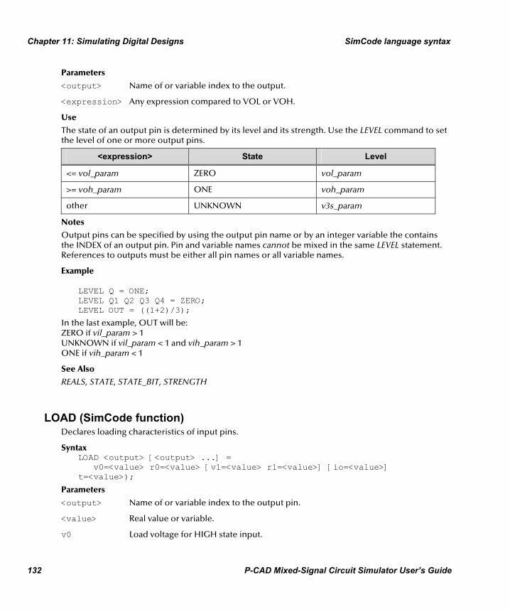
Chapter 11: Simulating Digital Designs SimCode language syntax
132 P-CAD Mixed-Signal Circuit Simulator User’s Guide
Parameters
<output> Name of or variable index to the output.
<expression> Any expression compared to VOL or VOH.
Use
The state of an output pin is determined by its level and its strength. Use the LEVEL command to set the level of one or more output pins.
<expression> State Level
<= vol_param ZERO vol_param
>= voh_param ONE voh_param
other UNKNOWN v3s_param
Notes
Output pins can be specified by using the output pin name or by an integer variable the contains the INDEX of an output pin. Pin and variable names cannot be mixed in the same LEVEL statement. References to outputs must be either all pin names or all variable names.
Example
LEVEL Q = ONE; LEVEL Q1 Q2 Q3 Q4 = ZERO; LEVEL OUT = ((1+2)/3);
In the last example, OUT will be: ZERO if vil_param > 1 UNKNOWN if vil_param < 1 and vih_param > 1 ONE if vih_param < 1
See Also
REALS, STATE, STATE_BIT, STRENGTH
LOAD (SimCode function) Declares loading characteristics of input pins.
Syntax LOAD <output> [<output> ...] = v0=<value> r0=<value> [v1=<value> r1=<value>] [io=<value>] t=<value>);
Parameters
<output> Name of or variable index to the output pin.
<value> Real value or variable.
v0 Load voltage for HIGH state input.
SimCode language syntax Chapter 11: Simulating Digital Designs
P-CAD Mixed-Signal Circuit Simulator User’s Guide 133
r0 Load resistance for HIGH state input.
v1 Load voltage for LOW state input.
r1 Load resistance for LOW state input
io Off-state load resistance for unused load.
t Time delay before the load will be applied.
Use
The LOAD command is typically used with input or power pins to provide loading for the driving circuit. Since only output pins can provide a load, each input must have a corresponding output. These are assigned using the IO_PAIRS statement.
If different loads are required for different inputs, multiple LOAD statements may be used. Power pins should be placed in a separate LOAD statement which does not include the v1/r1 load or io. Power pins are not included in the IO_PAIRS statement. The IO_PAIRS statement must be entered before any LOAD statements that contain io.
Notes
An input load consists of a voltage and a resistance (v0/r0 or v1/r1). The voltage level of the incoming signal determines which load will be used. If the voltage level goes below VIL and remains below VIH, then the input is considered to be in the LOW state and the v1/r1 is applied. If the voltage level goes above VIH and remains above VIL, then the input is considered to be in the HIGH state and the v0/r0 is applied. io is the input state off resistance. The unused load is essentially removed from the circuit by changing its r value to the value specified for io.
The values for v0, r0, v1 and r1 can be either real constants or real variables. The values for io and t must be real constants. Pin names and pin variables cannot be mixed in the same LOAD statement. References to outputs must be either all pin names or all variable names.
For input pins, the values used for r0 should be derived using the databook specs for IIH. A standard LS input, for example, will sink a maximum of 20uA at Vin=2.7V. Therefore, if vol_param = 0.2V, then:
for max HIGH state load: r0 = (Vin - vol_param) / IIHmax
r0 = (2.7V - 0.2V) / 20uA
r0 = 125k ohms
The values used for r1 should be derived using the databook specs for IIL. A standard LS input, for example, will source a maximum of 400uA at Vin=0.4V. Therefore, if voh_param = 4.6V then:
for max LOW state load: r1 = (voh_param - Vin) / IILmax
r1 = (4.6V - 0.4V) / 400uA
r1 = 10.5k ohms
For power pins, the value used for r0 should be derived using the databook specs for ICC. For a 74LS151, Icc typ is 6mA at Vcc=5V and Icc max is 10mA at Vcc=5.25V. Therefore:

Chapter 11: Simulating Digital Designs SimCode language syntax
134 P-CAD Mixed-Signal Circuit Simulator User’s Guide
for Icc typ: r0 = 5V / 6mA = 833 ohms
for Icc max: r0 = 5.25V / 10mA = 525 ohms
If creating a multiple-parts-per-package device, such as a 74LS00 quad NAND gate, you should adjust the Icc load for the individual parts accordingly.
Example
r0_val = (MIN_TYP_MAX(ld_param: NULL, NULL, 125k); r1_val = (MIN_TYP_MAX(ld_param: NULL, NULL, 10.5k); ricc_val = (MIN_TYP_MAX(ld_param: NULL, 833, 525); LOAD PRE_LD DATA_LD CLK_LD CLR_LD = (v0=vol_param, r0=r0_val, v1=voh_param, r1=r1_val, io=1e9, t=1p); LOAD VCC_LD = (v0=gnd_param, r0=ricc_val, t=1p);
See Also
IO_PAIRS , DRIVE
MATH FUNCTIONS (SimCode function) The following mathematical functions can be used in SimCode models:
Function Use Example
POW power X= (12 POW(3));
ABS absolute value X= (ABS(-12));
SQRT square-root X= (SQRT(2));
EXP exponent X= (EXP(10));
LOG natural log X= (LOG(0.1));
LOG10 log base 10 X= (LOG10(0.1));
SIN sine X= (SIN(0.1));
COS cosine X= (COS(0.1));
TAN tangent X= (TAN(0.1));
ASIN arc sine X= (ASIN(0.1));
ACOS arc cosine X= (ACOS(0.1));
ATAN arc tangent X= (ATAN(0.1));
HSIN hyperbolic sine X= (HSIN(0.1));
HCOS hyperbolic cosine X= (HCOS(0.1));
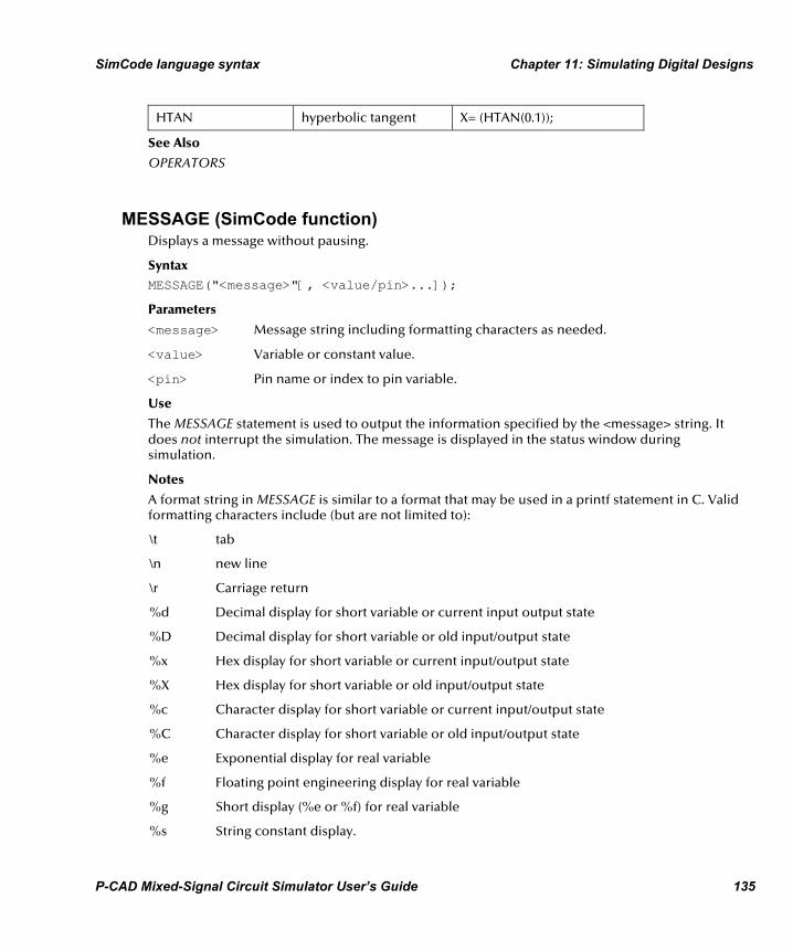
SimCode language syntax Chapter 11: Simulating Digital Designs
P-CAD Mixed-Signal Circuit Simulator User’s Guide 135
HTAN hyperbolic tangent X= (HTAN(0.1));
See Also
OPERATORS
MESSAGE (SimCode function) Displays a message without pausing.
Syntax MESSAGE("<message>"[, <value/pin>...]);
Parameters
<message> Message string including formatting characters as needed.
<value> Variable or constant value.
<pin> Pin name or index to pin variable.
Use
The MESSAGE statement is used to output the information specified by the <message> string. It does not interrupt the simulation. The message is displayed in the status window during simulation.
Notes
A format string in MESSAGE is similar to a format that may be used in a printf statement in C. Valid formatting characters include (but are not limited to):
\t tab
\n new line
\r Carriage return
%d Decimal display for short variable or current input output state
%D Decimal display for short variable or old input/output state
%x Hex display for short variable or current input/output state
%X Hex display for short variable or old input/output state
%c Character display for short variable or current input/output state
%C Character display for short variable or old input/output state
%e Exponential display for real variable
%f Floating point engineering display for real variable
%g Short display (%e or %f) for real variable
%s String constant display.

Chapter 11: Simulating Digital Designs SimCode language syntax
136 P-CAD Mixed-Signal Circuit Simulator User’s Guide
Note: The only valid string constants are:
INSTANCE The present SimCode device instance name.
FUNC The present SimCode device function name.
FILE The present SimCode device file name.
Examples MESSAGE("time\t\tCLK\tDATA\tQ\tQN");
MESSAGE("device instance= %s",INSTANCE);
MESSAGE("%.3e\t%d\t%d\t%d\t%d",present_time,CLK,DATA,Q,QN);
________________________________
See Also
PROMPT
MIN_TYP_MAX (SimCode function) Returns value from MIN_TYP_MAX look-up table.
Syntax MIN_TYP_MAX(<index>: <min>, <typ>, <max>);
Parameters
<index> Input variable (index to select min, typ or max values).
<min> Minimum databook value.
<typ> Typical databook value.
<max> Maximum databook value.
Use
The MIN_TYP_MAX function is similar to the SELECT_VALUE function except that three (3) values/variables must be entered. The keyword “NULL” can be substituted for one or two unknown values. If a predefined integer variable (see INTEGERS) is used as the <index>, unknown (NULL) values are calculated from the known values as follows:
Known Values Formula
<min>, <max> typical = (<max> + <min>) / 2;
<min> only typical = (<min> / <min scale factor>) maximum = (<min> / <min scale factor>) * <max scale factor>
<typ> only minimum = (<typ> * <min scale factor>) maximum = (<typ> * <max scale factor>)
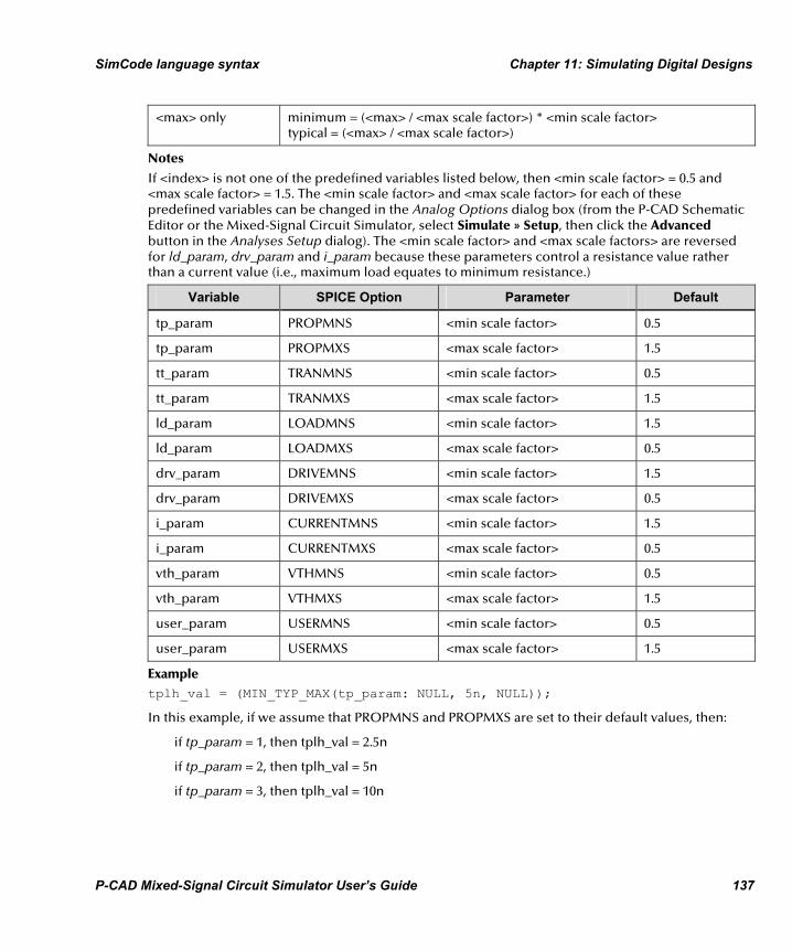
SimCode language syntax Chapter 11: Simulating Digital Designs
P-CAD Mixed-Signal Circuit Simulator User’s Guide 137
<max> only minimum = (<max> / <max scale factor>) * <min scale factor> typical = (<max> / <max scale factor>)
Notes
If <index> is not one of the predefined variables listed below, then <min scale factor> = 0.5 and <max scale factor> = 1.5. The <min scale factor> and <max scale factor> for each of these predefined variables can be changed in the Analog Options dialog box (from the P-CAD Schematic Editor or the Mixed-Signal Circuit Simulator, select Simulate » Setup, then click the Advanced button in the Analyses Setup dialog). The <min scale factor> and <max scale factors> are reversed for ld_param, drv_param and i_param because these parameters control a resistance value rather than a current value (i.e., maximum load equates to minimum resistance.)
Variable SPICE Option Parameter Default
tp_param PROPMNS <min scale factor> 0.5
tp_param PROPMXS <max scale factor> 1.5
tt_param TRANMNS <min scale factor> 0.5
tt_param TRANMXS <max scale factor> 1.5
ld_param LOADMNS <min scale factor> 1.5
ld_param LOADMXS <max scale factor> 0.5
drv_param DRIVEMNS <min scale factor> 1.5
drv_param DRIVEMXS <max scale factor> 0.5
i_param CURRENTMNS <min scale factor> 1.5
i_param CURRENTMXS <max scale factor> 0.5
vth_param VTHMNS <min scale factor> 0.5
vth_param VTHMXS <max scale factor> 1.5
user_param USERMNS <min scale factor> 0.5
user_param USERMXS <max scale factor> 1.5
Example tplh_val = (MIN_TYP_MAX(tp_param: NULL, 5n, NULL));
In this example, if we assume that PROPMNS and PROPMXS are set to their default values, then:
if tp_param = 1, then tplh_val = 2.5n
if tp_param = 2, then tplh_val = 5n
if tp_param = 3, then tplh_val = 10n

Chapter 11: Simulating Digital Designs SimCode language syntax
138 P-CAD Mixed-Signal Circuit Simulator User’s Guide
ricch_val = (MIN_TYP_MAX(i_param: NULL, 2500, 1250));
In this example, if we assume that CURRENTMNS and CURRENTMXS are set to their default values, then:
if i_param = 1, then ricch_val = 5000
if i_param = 2, then ricch_val = 2500
if i_param = 3, then ricch_val = 1250
See Also
INTEGERS, SELECT_VALUE
NO_CHANGE (SimCode function) Leaves output state of I/O pins unchanged.
Syntax NO_CHANGE <output> [<output> ...];
Parameters
<output> Name of or variable index to the output pin.
Use
Use the NO_CHANGE function to indicate no-change for specified output pins. Use this statement on bi-directional pins when the bi-directional pin is being treated as an input.
Notes
Pin names and variables cannot be mixed in the same NO_CHANGE statement. References to outputs must be either all pin names or all variable names.
Example NO_CHANGE Q1 Q2 Q3 Q4;
NUMBER (SimCode function) Returns number based on binary weighted pin states.
Syntax NUMBER(<MSB pin>, [<pin>, ...] <LSB pin> );
Parameters
<pin> Name of or index to a pin.

SimCode language syntax Chapter 11: Simulating Digital Designs
P-CAD Mixed-Signal Circuit Simulator User’s Guide 139
Use
The NUMBER function returns a short integer that represents the decimal value of the binary number represented by the list of <pin>. Each bit (represented by a <pin>) is set to 1 if the <pin> is non-zero, otherwise it is set to 0.
Notes
The first <pin> in the list represents the most significant bit (MSB) and the last <pin> in the list represents the least significant bit (LSB).
Example A = (NUMBER(D3,D2,D1,D0));
In this example, if D3 is HIGH, and D2, D1 and D0 are LOW (10002), then A = 8.
OPERATORS (SimCode function) The following operators can be used in SimCode expressions:
= Equals (sets a variable or output pin to a value or state).
+ Add
- Subtract
* Multiply
/ Divide
{tilde} Logical not
! Bitwise complement
&& AND
|| OR
^^ XOR
Bitwise Operators
& AND
| OR
^ XOR
<< Shift left
>> Shift right
Relative Comparators
= Equal
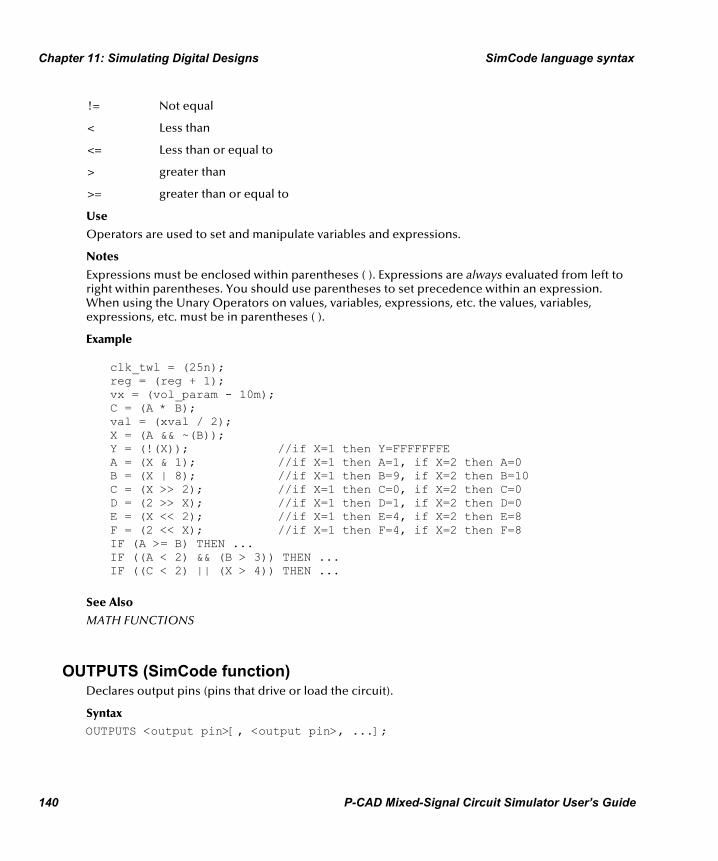
Chapter 11: Simulating Digital Designs SimCode language syntax
140 P-CAD Mixed-Signal Circuit Simulator User’s Guide
!= Not equal
< Less than
<= Less than or equal to
> greater than
>= greater than or equal to
Use
Operators are used to set and manipulate variables and expressions.
Notes
Expressions must be enclosed within parentheses ( ). Expressions are always evaluated from left to right within parentheses. You should use parentheses to set precedence within an expression. When using the Unary Operators on values, variables, expressions, etc. the values, variables, expressions, etc. must be in parentheses ( ).
Example
clk_twl = (25n); reg = (reg + 1); vx = (vol_param - 10m); C = (A * B); val = (xval / 2); X = (A && ~(B)); Y = (!(X)); //if X=1 then Y=FFFFFFFE A = (X & 1); //if X=1 then A=1, if X=2 then A=0 B = (X | 8); //if X=1 then B=9, if X=2 then B=10 C = (X >> 2); //if X=1 then C=0, if X=2 then C=0 D = (2 >> X); //if X=1 then D=1, if X=2 then D=0 E = (X << 2); //if X=1 then E=4, if X=2 then E=8 F = (2 << X); //if X=1 then F=4, if X=2 then F=8 IF (A >= B) THEN ... IF ((A < 2) && (B > 3)) THEN ... IF ((C < 2) || (X > 4)) THEN ...
See Also
MATH FUNCTIONS
OUTPUTS (SimCode function) Declares output pins (pins that drive or load the circuit).
Syntax OUTPUTS <output pin>[, <output pin>, ...];
SimCode language syntax Chapter 11: Simulating Digital Designs
P-CAD Mixed-Signal Circuit Simulator User’s Guide 141
Parameters
<output pin> Name of the output pin.
Use
The OUTPUTS data type is used to define the pins which affect the operation of circuitry external to the device. These generally include input, output, I/O and power pins. Input and power pins are included in this list because their presence constitutes a load on the driving circuitry.
Notes
Output pin names must begin with a letter and be defined before they are used.
Example OUTPUTS VCC_LD, PRE_LD, DATA_LD, CLK_LD, CLR_LD, QN, Q;
See Also
INPUTS , IO_PAIRS , PWR_GND_PINS
PARAM_SET (SimCode function) Syntax PARAM_SET(<param var>)
Parameters
<param var> SimCode model definition parameter.
Use
Determines if a predefined SimCode parameter has been set. The PARAM_SET function is used to determine if a parameter in the SimCode model definition has been set. It returns 1 if the specified parameter was set (e.g., vil_param=0.8) otherwise it returns 0.
Notes
See INTEGER and REAL declarations for a list of SimCode model definition parameters and their associated variable names.
Example A = PARAM_SET(ld_param);
IF (PARAM_SET(voh_param)) THEN ...
See Also
INTEGERS , REALS
PROMPT (SimCode function) Pauses simulation and displays a message.

Chapter 11: Simulating Digital Designs SimCode language syntax
142 P-CAD Mixed-Signal Circuit Simulator User’s Guide
Syntax PROMPT("<message>"[, <value/pin>...]);
Parameters
<message> Message string including formatting characters as needed.
<value> Variable or constant value.
<pin> Pin name or index to pin variable.
Use
The PROMPT statement is used to stop simulation and display the information specified by the <message> string. The message is displayed in the status window during simulation. The User must click on a button to continue execution of the SimCode.
Notes
A format string in PROMPT is similar to a format that may be used in a printf statement in C. Valid formatting characters include (but are not limited to):
\t tab
\n new line
\r carriage return
%d Decimal display for short variable or current input/output state.
%D Decimal display for short variable or old input/output state.
%x Hex display for short variable or current input/output state.
%X Hex display for short variable or old input/output state.
%c Character display for short variable or current input/output state.
%C Character display for short variable or old input/output state.
%e Exponential display for real variable.
%f Floating point engineering display for real variable.
%g Short display (%e or %f) for real variable.
%s String constant display.
Note: The only valid string constants are:
INSTANCE The present SimCode device instance name.
FUNC The present SimCode device function name.
FILE The present SimCode device file name.
Example PROMPT("input=%d time=%f device=%s", D1, t1, INSTANCE);
SimCode language syntax Chapter 11: Simulating Digital Designs
P-CAD Mixed-Signal Circuit Simulator User’s Guide 143
See Also
MESSAGE
PWL_TABLE (SimCode function) Returns value from interpolative look-up table.
Syntax PWL_TABLE (<IN var>: <IN1>,<OUT1>,<IN2>,<OUT2>[,...<OUTn>,<OUTn>])
Parameters
<IN var> input variable (integer or real)
<INx> input compare value
<OUTx> output value at <INx>
Use
Returns value from interpolative look-up table. This piece-wise-linear function is essentially a look-up table. The value of <IN var> is used to look up an entry in the table which consists of pairs of values. The first value in each pair is an input compare value and the second value is the corresponding output value. If the <IN var> value is less than the first <IN> value, the first <OUT> value is returned. If the <IN var> value is greater than the last <INn> value then the last <OUTn> value is returned. Linear interpolation is done between entries according to the formula:
value = (((OUTA-OUTB)/(INA-INB))*(<IN var>-INA)+OUTA)
where <IN var> falls between the input compare values INA and INB. The actual output value will fall between output values OUTA and OUTB.
Notes
Two or more IN/OUT data value pairs must be entered and the IN values must be entered in ascending order. There is no limit to the maximum number of IN/OUT data pairs that can be entered.
Example twh = (PWL_TABLE(var: 5,180n,10,120n,15,80n));
In this example, if var = 10 then twh = 120n and if var = 12 then twh = 104.
See Also
SELECT_VALUE
PWR_GND_PINS (SimCode function) Declares power and ground pins; records supply voltage.
Chapter 11: Simulating Digital Designs SimCode language syntax
144 P-CAD Mixed-Signal Circuit Simulator User’s Guide
Syntax PWR_GND_PINS (<pwrpin>, <gndpin>);
Parameters
<pwrpin> name of the power pin
<gndpin> name of the ground pin
Use
The PWR_GND_PINS statement defines which of the INPUTS pins are power and ground and sets the Power and Ground parameters of the device to absolute voltages as follows:
pwr_param = voltage on <pwrpin>
gnd_param = voltage on <gndpin>
Notes
This statement can only be used once in the SimCode. Only one pin can be defined for power and one for ground.
Example PWR_GND_PINS(VCC, GND);
See Also
INPUTS, OUTPUTS, REALS, VIL_VIH_PERCENT, SUPPLY_MIN_MAX
READ_DATA (SimCode function) Reads data from an ASCII file into arrays.
Syntax READ_DATA(<array>[, <array>, ...])
Parameters
<array> Name of the array into which the value is placed.
Use
The READ_DATA function opens the file specified by the “data=” parameter in the device’s .MODEL statement and reads ASCII text data. The number and type (integer/real) of the values per line that will be read is based on the number and type of array variables that are specified in the function call. The number of data lines read is determined by the number of data lines in the specified file and/or the size of the smallest array in the function call. The READ_DATA function returns the number of lines read. A negative number is returned if an error is encountered:
-1 Invalid file name
-2 Can’t find file
-3 Invalid array
SimCode language syntax Chapter 11: Simulating Digital Designs
P-CAD Mixed-Signal Circuit Simulator User’s Guide 145
-4 Illegal array access
-5 Data type
-6 Expected data value
Notes
Multiple values per line in the data file must be separated by commas. The real values in the data file must be in scientific notation. The device’s .MODEL statement which contains the “data=” parameter must be placed in the device symbol’s .MDL file.
Example
MYDEVICE.MDL file:
.MODEL AMYDEVICE XSIMCODE(file="{MODEL_PATH}MYDEVICES.SCB"
+ func=MyDevice data="{MODEL_PATH}MYDEVICE.DAT" {mntymx})
MYDEVICE.DAT file:
8, 8E-6
9, 9E-6
10, 1E-5
11, 1.1E-5
MyDevice SimCode:
nlines = READ_DATA(int_array, real_array);
This example opens a file called MYDEVICE.DAT in the Models directory. It reads two columns of data from the file where the first column contains integer values and the second column contains real values. If the arrays are declared as int_array[3] and real_array[5] then only the first three data lines will be read and nlines will be set to 3.
REALS (SimCode function) The REALS data type is used to define real variables and arrays.
Syntax REALS <var>[, <var>, ...];
Parameters
<var> name of the variable
Notes
Real variables and arrays must begin with a letter and be defined before they are used. Real arrays are defined by following the array name with a left bracket ( [ ), an integer number which defines the size of the array, and a right bracket ( ] ). Real arrays can be set and/or used in expressions.
The following are reserved SimCode real variables that do not need to be declared:
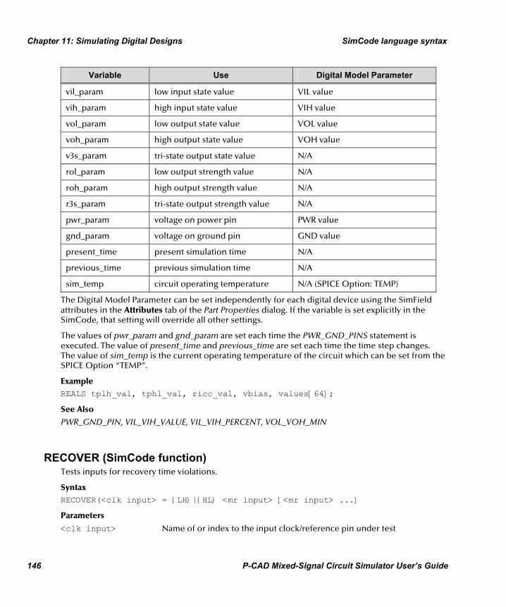
Chapter 11: Simulating Digital Designs SimCode language syntax
146 P-CAD Mixed-Signal Circuit Simulator User’s Guide
Variable Use Digital Model Parameter
vil_param low input state value VIL value
vih_param high input state value VIH value
vol_param low output state value VOL value
voh_param high output state value VOH value
v3s_param tri-state output state value N/A
rol_param low output strength value N/A
roh_param high output strength value N/A
r3s_param tri-state output strength value N/A
pwr_param voltage on power pin PWR value
gnd_param voltage on ground pin GND value
present_time present simulation time N/A
previous_time previous simulation time N/A
sim_temp circuit operating temperature N/A (SPICE Option: TEMP)
The Digital Model Parameter can be set independently for each digital device using the SimField attributes in the Attributes tab of the Part Properties dialog. If the variable is set explicitly in the SimCode, that setting will override all other settings.
The values of pwr_param and gnd_param are set each time the PWR_GND_PINS statement is executed. The value of present_time and previous_time are set each time the time step changes. The value of sim_temp is the current operating temperature of the circuit which can be set from the SPICE Option “TEMP”.
Example REALS tplh_val, tphl_val, ricc_val, vbias, values[64];
See Also
PWR_GND_PIN, VIL_VIH_VALUE, VIL_VIH_PERCENT, VOL_VOH_MIN
RECOVER (SimCode function) Tests inputs for recovery time violations.
Syntax RECOVER(<clk input> = {LH}|{HL} <mr input> [<mr input> ...]
Parameters
<clk input> Name of or index to the input clock/reference pin under test
SimCode language syntax Chapter 11: Simulating Digital Designs
P-CAD Mixed-Signal Circuit Simulator User’s Guide 147
<mr input> Name of or index to the input set/reset pin under test.
TREC Recovery time for both low and high going <mr pin>.
TRECL Recovery time for low going <mr pin>.
TRECH Recovery time for high going <mr pin>.
<message> Text string that will be displayed if a warning occurs.
Use
The RECOVER function compares the time difference between a level change (LH or HL) on the <clk input> and a level change on the <mr input> to a specified test time. RECOVER test times are specified jointly using TREC=<time> (which sets TRECL and TRECH to the same value) or individually using TRECL=<time> and TRECH=<time>. If the compare time is less than the specified <time> a warning will be displayed during simulation. An optional <message> string can be included in the RECOVER statement which will be output if a warning is displayed.
Notes
Databook specifications should be used with this function. TRECL=<time> and TRECH=<time> can be entered in the same RECOVER test. The RECOVER test will be made only if the state of the <mr input> matches the time parameter (TRECL=LOW, TRECH=HIGH) when the <clk input> makes the specified transition (LH or HL). For Example, if <clk input> = LH and TRECL is specified then the <mr input> must be LOW when the <clk input> goes from LOW to HIGH for a RECOVER test to be made. Pin names and variables can be mixed in the same RECOVER statement.
Example RECOVER(CLK=LH PRE CLR TREC=trec_val
"CLK->PRE or CLR");
RETURN (SimCode function) Returns from a subroutine in the SimCode.
Syntax RETURN
Use
The RETURN instruction is used to return program flow to the instruction that followed the last GOSUB instruction.
See Also
GOSUB
SELECT_VALUE (SimCode function) Returns value from simple look-up table.

Chapter 11: Simulating Digital Designs SimCode language syntax
148 P-CAD Mixed-Signal Circuit Simulator User’s Guide
Syntax SELECT_VALUE (<index>: <val/pin/var>,
<val/pin/var>[,<val/pin/var>,...]);
Parameters
<index> input variable (index to <val/pin/var>)
<val/pin/var> output value, pin or variable
Use
The SELECT_VALUE function returns the value of the number or variable indicated by the value of the index variable.
Notes
The number of values and/or variables used is not limited.
Example A = (SELECT_VALUE(B: 16, 8, 4, 2, 1));
In this example, if B = 2 then A = 8 (the 2nd value).
See Also
PWL_TABLE, MIN_TYP_MAX
SETUP_HOLD (SimCode function) Tests inputs for setup and hold time violations
Syntax SETUP_HOLD(<clk input> = {LH}|{HL}
<data input> [<data input> ...]
{TS=<time>}|{TSL=<time> TSH=<time>}
{TH=<time>}|{THL=<time> THH=<time>} ["<message>"];
Parameters
<clk input> Name of or index to the input clock/reference pin under test.
<data input> Name of or index to the input data pin under test.
TS Setup time for both low and high going <data input>.
TSL Setup time for low going <data input>.
TSH Setup time for high going <data input>.
TH Hold time for both low and high going <data input>.
THL Hold time for high going <data input>.

SimCode language syntax Chapter 11: Simulating Digital Designs
P-CAD Mixed-Signal Circuit Simulator User’s Guide 149
THH Hold time for low going <data input>.
<message> Text string that will be displayed if a warning occurs.
Use
The SETUP_HOLD function compares the time difference between a level change (LH or HL) on the <clk input> and a level change on the <data input> to a specified test time. SETUP test times are specified jointly using TS=<time> (which sets TSL and TSH to the same value) or individually using TSL=<time> and TSH=<time>. HOLD test times are specified jointly using TH=<time> (which sets THL and THH to the same value) or individually using THL=<time> and THH=<time>. If the compare time is less than the specified <time> a WARNING will be displayed. An optional <message> string can be included in a SETUP_HOLD statement which will be output if a WARNING is displayed.
Notes
Databook specifications should be used with this function. TSL=<time>, TSH=<time>, THL=<time> and THH=<time> can be entered in the same SETUP_HOLD statement. The SETUP and/or HOLD test will be made only if the state of the <data input> matches the time parameter (TSL or THL=LOW, TSH or THH=HIGH) when the <clk input> makes the specified transition (LH or HL). For Example, if <clk input>=LH and TSL is specified, then the <data input> must be LOW when the <clk input> goes from LOW to HIGH for a SETUP test to be made. Pin names and variables can be mixed in the same SETUP_HOLD statement.
Example SETUP_HOLD(CLK=LH DATA Ts=ts_val Th=th_val "CLK->DATA");
STATE (SimCode function) Sets outputs to the declared logic state.
Syntax 1 STATE <output> [<output>...] = (<expression>);
Syntax 2 STATE <output> [<output>...] = {ZERO}|{ONE}|{UNKNOWN};
Parameters:
<output> Name of or variable index to the output pin.
<expression> Any expression to be compared to VIL or VIH.
Use
The state of an output pin is determined by its level and its strength. The STATE command sets the level and strength for one or more output pins or variables. If <expression> is less than or equal to vil_param, the output will be set to ZERO. If <expression> is greater than or equal to vih_param, the output will be set to ONE. Otherwise, the output will be set to UNKNOWN. The level and strength values are set according the state:

Chapter 11: Simulating Digital Designs SimCode language syntax
150 P-CAD Mixed-Signal Circuit Simulator User’s Guide
<expression> State Level Strength
<= vol_param ZERO vol_param rol_param
>= voh_param ONE voh_param roh_param
other UNKNOWN v3s_param r3s_param
Notes
Output pins can be specified by using the output pin name or by an integer variable that contains the index of an output pin. Pin and variable names cannot be mixed in the same STATE command. References to outputs must be either all pin names or all variable names.
Example STATE Q = ONE;
STATE Q1 Q2 Q3 Q4 = ZERO;
STATE OUT = ((1+2)/3);
In the last example, OUT will be:
ZERO if vil_param > 1
UNKNOWN if vil_param < 1 and vih_param > 1
ONE if vih_param < 1
See Also
REALS , STATE_BIT , LEVEL , STRENGTH , TABLE , EXT_TABLE
STATE_BIT (SimCode function) Sets outputs to binary weighted logic states.
Syntax STATE_BIT <output> [<output> ...] = (<expression>) ;
Parameters
<output> name of or variable index to the output pin
<expression> any expression which can be bitwise matched with the outputs
Use
The state of an output pin is determined by its level and its strength. The STATE_BIT command is used to set the level and strength for one or more output pins based on the value of the <expression>. The state of the first pin listed is set according to the first (least-significant-bit) of the expression's value, the state of the second pin listed is set according to second bit of the expression's value, and so on. The level and strength values are set by the bit's value:
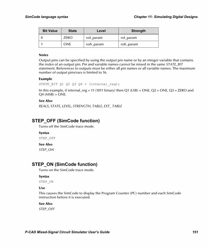
SimCode language syntax Chapter 11: Simulating Digital Designs
P-CAD Mixed-Signal Circuit Simulator User’s Guide 151
Bit Value State Level Strength
0 ZERO vol_param rol_param
1 ONE voh_param roh_param
Notes
Output pins can be specified by using the output pin name or by an integer variable that contains the index of an output pin. Pin and variable names cannot be mixed in the same STATE_BIT statement. References to outputs must be either all pin names or all variable names. The maximum number of output pins/vars is limited to 16.
Example STATE_BIT Q1 Q2 Q3 Q4 = (internal_reg);
In this example, if internal_reg = 11 (1011 binary) then Q1 (LSB) = ONE, Q2 = ONE, Q3 = ZERO and Q4 (MSB) = ONE.
See Also
REALS, STATE, LEVEL, STRENGTH, TABLE, EXT_ TABLE
STEP_OFF (SimCode function) Turns off the SimCode trace mode.
Syntax STEP_OFF
See Also
STEP_ON
STEP_ON (SimCode function) Turns on the SimCode trace mode.
Syntax STEP_ON
Use
This causes the SimCode to display the Program Counter (PC) number and each SimCode instruction before it is executed.
See Also
STEP_OFF
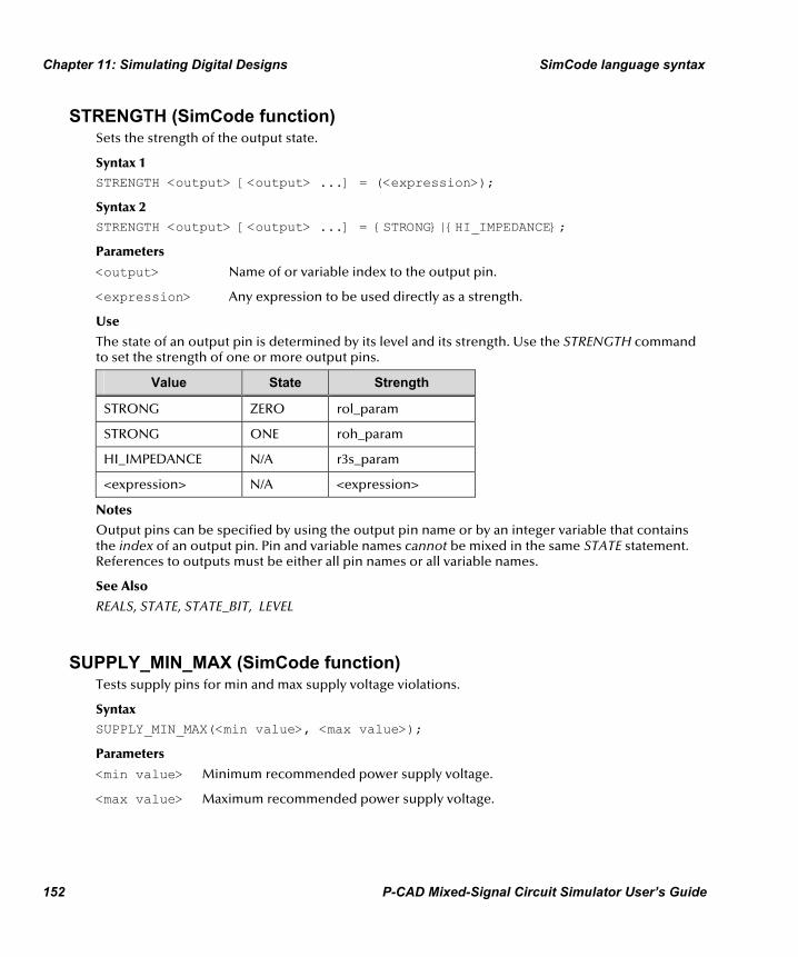
Chapter 11: Simulating Digital Designs SimCode language syntax
152 P-CAD Mixed-Signal Circuit Simulator User’s Guide
STRENGTH (SimCode function) Sets the strength of the output state.
Syntax 1 STRENGTH <output> [<output> ...] = (<expression>);
Syntax 2 STRENGTH <output> [<output> ...] = {STRONG}|{HI_IMPEDANCE};
Parameters
<output> Name of or variable index to the output pin.
<expression> Any expression to be used directly as a strength.
Use
The state of an output pin is determined by its level and its strength. Use the STRENGTH command to set the strength of one or more output pins.
Value State Strength
STRONG ZERO rol_param
STRONG ONE roh_param
HI_IMPEDANCE N/A r3s_param
<expression> N/A <expression>
Notes
Output pins can be specified by using the output pin name or by an integer variable that contains the index of an output pin. Pin and variable names cannot be mixed in the same STATE statement. References to outputs must be either all pin names or all variable names.
See Also
REALS, STATE, STATE_BIT, LEVEL
SUPPLY_MIN_MAX (SimCode function) Tests supply pins for min and max supply voltage violations.
Syntax SUPPLY_MIN_MAX(<min value>, <max value>);
Parameters
<min value> Minimum recommended power supply voltage.
<max value> Maximum recommended power supply voltage.
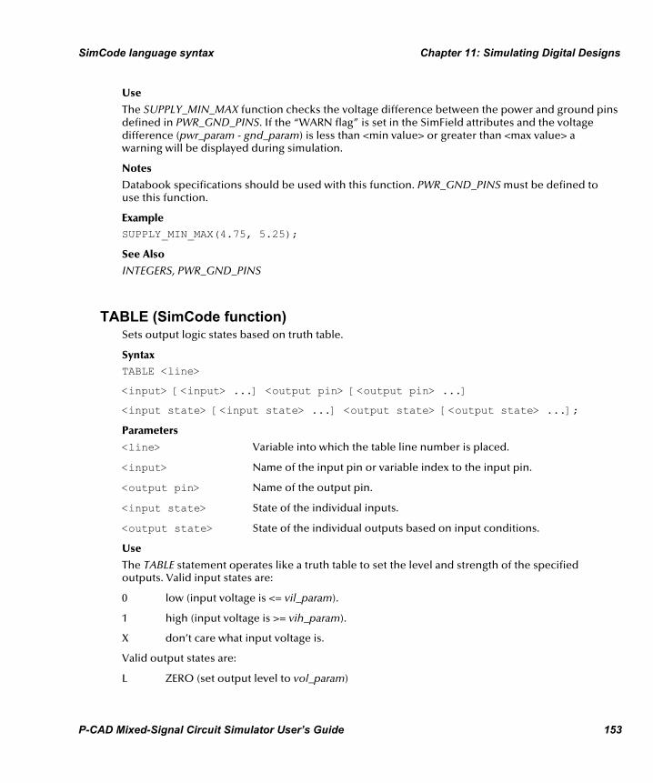
SimCode language syntax Chapter 11: Simulating Digital Designs
P-CAD Mixed-Signal Circuit Simulator User’s Guide 153
Use
The SUPPLY_MIN_MAX function checks the voltage difference between the power and ground pins defined in PWR_GND_PINS. If the “WARN flag” is set in the SimField attributes and the voltage difference (pwr_param - gnd_param) is less than <min value> or greater than <max value> a warning will be displayed during simulation.
Notes
Databook specifications should be used with this function. PWR_GND_PINS must be defined to use this function.
Example SUPPLY_MIN_MAX(4.75, 5.25);
See Also
INTEGERS, PWR_GND_PINS
TABLE (SimCode function) Sets output logic states based on truth table.
Syntax TABLE <line>
<input> [<input> ...] <output pin> [<output pin> ...]
<input state> [<input state> ...] <output state> [<output state> ...];
Parameters
<line> Variable into which the table line number is placed.
<input> Name of the input pin or variable index to the input pin.
<output pin> Name of the output pin.
<input state> State of the individual inputs.
<output state> State of the individual outputs based on input conditions.
Use
The TABLE statement operates like a truth table to set the level and strength of the specified outputs. Valid input states are:
0 low (input voltage is <= vil_param).
1 high (input voltage is >= vih_param).
X don’t care what input voltage is.
Valid output states are:
L ZERO (set output level to vol_param)
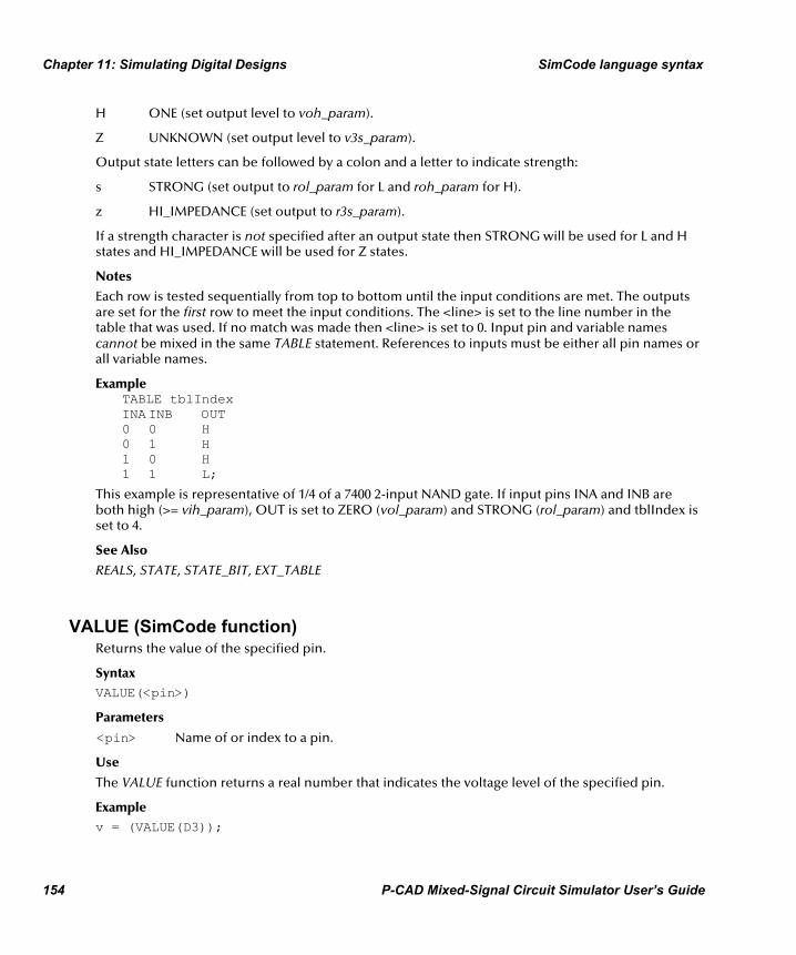
Chapter 11: Simulating Digital Designs SimCode language syntax
154 P-CAD Mixed-Signal Circuit Simulator User’s Guide
H ONE (set output level to voh_param).
Z UNKNOWN (set output level to v3s_param).
Output state letters can be followed by a colon and a letter to indicate strength:
s STRONG (set output to rol_param for L and roh_param for H).
z HI_IMPEDANCE (set output to r3s_param).
If a strength character is not specified after an output state then STRONG will be used for L and H states and HI_IMPEDANCE will be used for Z states.
Notes
Each row is tested sequentially from top to bottom until the input conditions are met. The outputs are set for the first row to meet the input conditions. The <line> is set to the line number in the table that was used. If no match was made then <line> is set to 0. Input pin and variable names cannot be mixed in the same TABLE statement. References to inputs must be either all pin names or all variable names.
Example TABLE tblIndex INA INB OUT 0 0 H 0 1 H 1 0 H 1 1 L;
This example is representative of 1/4 of a 7400 2-input NAND gate. If input pins INA and INB are both high (>= vih_param), OUT is set to ZERO (vol_param) and STRONG (rol_param) and tblIndex is set to 4.
See Also
REALS, STATE, STATE_BIT, EXT_TABLE
VALUE (SimCode function) Returns the value of the specified pin.
Syntax VALUE(<pin>)
Parameters
<pin> Name of or index to a pin.
Use
The VALUE function returns a real number that indicates the voltage level of the specified pin.
Example v = (VALUE(D3));

SimCode language syntax Chapter 11: Simulating Digital Designs
P-CAD Mixed-Signal Circuit Simulator User’s Guide 155
VIL_VIH_PERCENT (SimCode function) Sets VIL and VIH values to a percentage of supply voltage.
Syntax VIL_VIH_PERCENT (<vil %>, <vih %>);
Parameters
<vil %> Percentage of the supply voltage which defines vil.
<vih %> Percentage of the supply voltage which defines vih.
Use
VIL and VIH do not use a min/typ/max array to select their values, but must be declared explicitly for each digital device. The VIL_VIH_PERCENT statement sets the VIL and VIH parameters of the device to a percentage of the supply voltage as follows:
vil_param = (pwr_param - gnd_param) * <vil %>
vih_param = (pwr_param - gnd_param) * <vih %>
Notes
PWR_GND_PINS must be defined to use this function. The % values must be greater than 0 and less than 100. The vil_param and vih_param values set by VIL_VIH_PERCENT are overridden by any values set for “VIL value” and “VIH value” in the SimField attributes.
Example VIL_VIH_PERCENT(33, 67);
See Also
REALS, PWR_GND_PINS
VIL_VIH_VALUE (SimCode function) Sets absolute VIL and VIH values.
Syntax VIL_VIH_VALUE (<vil>, <vih>);
Parameters
<vil> Absolute voltage level which defines vil.
<vih> Absolute voltage level which defines vih.
Use
VIL and VIH do not use a min/typ/max array to select their values, but must be declared explicitly for each digital device. The VIL_VIH_VALUE statement sets the VIL and VIH parameters of the device to absolute voltages as follows:
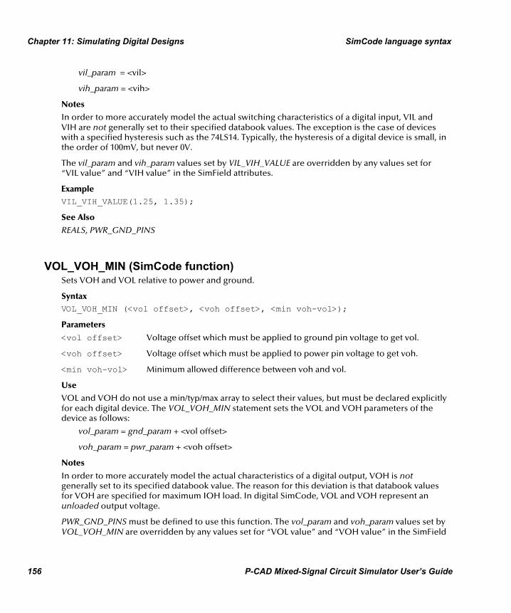
Chapter 11: Simulating Digital Designs SimCode language syntax
156 P-CAD Mixed-Signal Circuit Simulator User’s Guide
vil_param = <vil>
vih_param = <vih>
Notes
In order to more accurately model the actual switching characteristics of a digital input, VIL and VIH are not generally set to their specified databook values. The exception is the case of devices with a specified hysteresis such as the 74LS14. Typically, the hysteresis of a digital device is small, in the order of 100mV, but never 0V.
The vil_param and vih_param values set by VIL_VIH_VALUE are overridden by any values set for “VIL value” and “VIH value” in the SimField attributes.
Example VIL_VIH_VALUE(1.25, 1.35);
See Also
REALS, PWR_GND_PINS
VOL_VOH_MIN (SimCode function) Sets VOH and VOL relative to power and ground.
Syntax VOL_VOH_MIN (<vol offset>, <voh offset>, <min voh-vol>);
Parameters
<vol offset> Voltage offset which must be applied to ground pin voltage to get vol.
<voh offset> Voltage offset which must be applied to power pin voltage to get voh.
<min voh-vol> Minimum allowed difference between voh and vol.
Use
VOL and VOH do not use a min/typ/max array to select their values, but must be declared explicitly for each digital device. The VOL_VOH_MIN statement sets the VOL and VOH parameters of the device as follows:
vol_param = gnd_param + <vol offset>
voh_param = pwr_param + <voh offset>
Notes
In order to more accurately model the actual characteristics of a digital output, VOH is not generally set to its specified databook value. The reason for this deviation is that databook values for VOH are specified for maximum IOH load. In digital SimCode, VOL and VOH represent an unloaded output voltage.
PWR_GND_PINS must be defined to use this function. The vol_param and voh_param values set by VOL_VOH_MIN are overridden by any values set for “VOL value” and “VOH value” in the SimField
SimCode language syntax Chapter 11: Simulating Digital Designs
P-CAD Mixed-Signal Circuit Simulator User’s Guide 157
attributes. These are offset values rather than absolute voltages. The <voh offset> is negative so that when added to pwr_param, the resulting VOH will not be greater than pwr_param. If the difference between the resulting vol_param and voh_param is less than <min voh-vol>, then vol_param will be set to the value of gnd_param and voh_param will be set to gnd_param + <min voh-vol>.
Example VOL_VOH_MIN(0.2, -0.4, 0.1);
In this example: 1 If gnd_param = 0V and pwr_param = 5.0V, then vol_param = 0.2V and voh_param = 4.6V 2 If gnd_param = 0V and pwr_param = 0.5V, then vol_param = 0.0V and voh_param = 0.1V
See Also
REALS, PWR_GND_PINS
WHILE ... DO (SimCode function) Conditionally controls looping in the SimCode.
Syntax WHILE (<expression>) DO BEGIN ... END;
Parameters
<expression> Any expression that can be evaluated as true or false
Use
The WHILE ... DO statement is used to loop through a section of SimCode until <expression> evaluates to false.
Notes
Program flow will remain in a loop between the BEGIN and END statements until <expression> evaluates to false, then program flow resumes after the END statement.
Example i = 1; WHILE (i <= 5) DO BEGIN data[i] = data[i + 1]; i = i + 1; END;
See Also
IF ... THEN
Chapter 11: Simulating Digital Designs SimCode language syntax
158 P-CAD Mixed-Signal Circuit Simulator User’s Guide
WIDTH (SimCode function) Tests inputs for minimum pulse width violations.
Syntax WIDTH(<input> [<input>...] {TWL=<time>}|{TWH=<time>} ["<message>"];
Parameters
<input> Name of or variable index to the input pin under test.
TWL Width of a low going pulse.
TWH Width of a high going pulse.
<message> Text string that will be displayed if a warning occurs.
Use
The WIDTH function compares the pulse width on each <ipin> to the specified test WIDTH times. A low level test time is specified using TWL=<time> while a high level test time is specified using TWH=<time>. If the compare time is less than the specified <time> a WARNING will be displayed. An optional <message> string can be included in the WIDTH statement which will be output if a WARNING is displayed.
Notes
Databook specifications should be used with this function. The input pins can be input pin names and/or integer variables that contain an index value to an input pin. Pin names and variables can be mixed in the same WIDTH statement.
Example WIDTH(CLK TWL=clk_twl TWH=clk_twh "CLK");
WIDTH(PRE CLR TWL= pre_clr_twl "PRE or CLR");
WIDTH_TIME (SimCode function) Returns last pulse width encountered on specified pin.
Syntax WIDTH_TIME(<input>)
Parameters
<input> Name of or index to an input pin.
Use
This function returns a real value that indicates the last pulse width encountered on the specified <input>.
Example PW = (WIDTH_TIME(CP2)
P-CAD Mixed-Signal Circuit Simulator User’s Guide 159
CHAPTER 12
Design Explorer Text Editor and Macros
This chapter explores the powerful Text Editor and Macro server available in the Design Explorer.
The Design Explorer Text Editor The Design Explorer Text Editor is a feature-rich, professional text editor suitable for writing source code and as a general purpose text editing tool. The Text Editor includes the normal text editing facilities such as cutting, copying and pasting, search and replace.
It also includes a feature known as Syntax Highlighting. This feature allows you to highlight different elements in the document based on the syntax, where different word types, symbols and identifiers are assigned unique colors. This feature is an excellent document editing aid, particularly when working with documents with a repetitive, structured nature, such as macro scripts or source code. To broaden the usefulness of the syntax highlighting feature, the Text Editor allows the definition of multiple languages. Syntax highlighting can be uniquely configured for each of these languages.
Other Text Editor features include:
• User-definable code templates
• Three word wrap modes
• Auto indenting with smart tabs
• Block selection
• Regular expression support for Find and Replace
• Enhanced Undo
• Extended set of shortcut keys
• Enhanced print features, including print block, syntax printing and color printing.
The Text Editor menu commands appear when you have a text-editable document active in the Design Window. Also, you can click on the Browse Text tab to display commonly used commands.
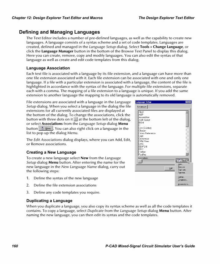
Chapter 12: Design Explorer Text Editor and Macros The Design Explorer Text Editor
160 P-CAD Mixed-Signal Circuit Simulator User’s Guide
Defining and Managing Languages The Text Editor includes a number of pre-defined languages, as well as the capability to create new languages. A language consists of a syntax scheme and a set of code templates. Languages are created, defined and managed in the Language Setup dialog. Select Tools » Change Language, or click the Language Manager button in the bottom of the Browse Text Panel to display this dialog. Here you can create, remove, copy and modify languages. You can also edit the syntax of that language as well as create and edit code templates from this dialog.
Language Association Each text file is associated with a language by its file extension, and a language can have more than one file extension associated with it. Each file extension can be associated with one and only one language. If a file with a particular extension is associated with a language, the content of the file is highlighted in accordance with the syntax of the language. For multiple file extensions, separate each with a comma. The mapping of a file extension to a language is unique. If you add the same extension to another language the mapping to its old language is automatically removed.
File extensions are associated with a language in the Language Setup dialog. When you select a language in the dialog the file extensions for all currently associated files are displayed at the bottom of the dialog. To change the associations, click the button with three dots on it at the bottom left of the dialog, or select Associations from the Language Setup dialog Menu button . You can also right click on a language in the list to pop up the dialog Menu.
The Edit Associations dialog displays, where you can Add, Edit, or Remove associations.
Creating a New Language To create a new language select New from the Language Setup dialog Menu button. After entering the name for the new language in the New Language Name dialog, carry out the following steps:
1. Define the syntax of the new language
2. Define the file extension associations
3. Define any code templates you require.
Duplicating a Language When you duplicate a language, you also copy its syntax scheme as well as all the code templates it contains. To copy a language, select Duplicate from the Language Setup dialog Menu button. After naming the new language, you can then edit its syntax and the code templates.

The Design Explorer Text Editor Chapter 12: Design Explorer Text Editor and Macros
P-CAD Mixed-Signal Circuit Simulator User’s Guide 161
Renaming a Language Renaming a language only changes the name of the language. To rename a language, select Rename from the Language Setup dialog Menu button.
Removing a Language When a language is removed, both its syntax and any code templates are also removed. Any file extensions associated with this language are also removed. Select Remove from the Language Setup dialog Menu button.
Syntax Highlighting Syntax highlighting is a method used to make text documents more readable, where different elements in the document are highlighted based on their syntax. The way this is done is to assign different words, symbols and identifiers a unique color. This set of color assignments is called that language’s syntax. The set of words, symbols and identifiers that make up the syntax are defined in the Syntax Editor dialog. Highlight colors are then assigned in the Text Editor Properties dialog, displayed by choosing Tools » Preferences.
The Syntax Editor dialog can be accessed directly by choosing Tools » Edit Language Syntax, or by double-clicking on a language name in the Language Setup dialog. The dialog is divided into a number of tabs, each representing a different area of the language’s syntax.
The syntax styles can be set by clicking on the Style buttons. See Defining the Syntax Style later in this chapter for more information.
Chapter 12: Design Explorer Text Editor and Macros The Design Explorer Text Editor
162 P-CAD Mixed-Signal Circuit Simulator User’s Guide
Options tab Use meta symbols for escapes
Meta symbols are symbols which can be inserted into a document, but which are not considered part of the document by the compiler that is being used. From the Text Editor’s perspective, they simply change the syntax highlighting used. The Text Editor supports the use of meta symbols in two ways:
1. To escape other syntax elements. For example if the ` character specifies the start of a string, putting a meta symbol before this will cancel this (e.g. \` if \ is the meta symbol).
2. To continue syntax elements over the end of a line. For example if {} is used to specify single line strings, the meta symbol can be used to extend a string over multiple lines.
Highlight directives
These are messages to the compiler which take up a whole line in the text document. To highlight directives in the Text Editor, first enable the Highlight Directives option and enter a character or set of characters that identify the start of a directive. All lines which start with these characters are then highlighted as directives.
Use symbols
These are all non-alpha numeric characters, like a plus sign, full stop, comma, and so on.
Use identifiers
Identifiers are all other strings that are not defined as Comments, Strings or Keywords.
Comments tab Comments are elements in the text file that you wish to define as code comments. These can be defined as single-line, full-line or multi-line comments. Comments are defined by their delimiters, that is the characters that indicate that a block of text is a comment. Single line and full-line comments only require a Left Delimiter (the other end is defined by an EOL character). Single line comments can commence anywhere on a line, full line comments require the comment Delimiter to be the first character on the line. Multi-line comments require a Left Delimiter and a Right Delimiter to define where they start and end. Multiple comment styles can be defined.
After defining the comment delimiters, you can edit the way that the comments present on screen by clicking the Style button at the bottom of the dialog. In the Edit Style dialog you can define the color and certain aspects of the comment font, such as the use of bold or italics.
Example: An example of each of the three types of comment is shown:
/ this is a multiline comment, where the slash characters define the start and end of the comment lines / case keyword is when "RESET" => Reset <= '1'; -- single line comment, the 2 dashes delimit the commment cycle(1); Reset <= '0';
The Design Explorer Text Editor Chapter 12: Design Explorer Text Editor and Macros
P-CAD Mixed-Signal Circuit Simulator User’s Guide 163
* this is a full line comment, the * character delimits the comment
Strings tab Strings are elements in the text file that you wish to define as strings in the code, such as strings that appear as a message in a dialog that your program displays. Both single-line and multi-line strings are supported, and both types require the left and right delimiters to define their start and end point. Multiple string styles can be defined.
After defining the string delimiters you can edit the way that strings present on screen by clicking the Style button at the bottom of the dialog. In the Edit Style dialog you can define the color and certain aspects of the string font, such as the use of bold or italics.
Example: In this example, the single quote characters delimit the start and end of the string.
if MessageDlg(Format('OK to overwrite %s', [SaveDialog.FileName]),
Numbers tab Like Comments and Strings, Numbers are another class of information in the text document that you may wish to make stand out. Simple numbers are defined as being strings of numeric digits, which may or may not contain a decimal point, for example “45”, “45.6” but not “45.6.6”. Simple numbers can also include an “E” character, denoting scientific notation, such as 53E3, or 24e6.
Special numbers are defined as having a prefix and/or a suffix and contain numerical digits, or the letters A-F. These could be used to tell a compiler that the number is hexadecimal or octal, for example. Examples of these numbers are “0xAF034AD”, “88j”, “j8A8y”, but not “0xA.4”.
Each number type is specified by a suffix, a prefix or a prefix/suffix combination. The basic behavior of prefixes and suffixes is that whenever a valid prefix or suffix is detected in combination with a number, then the number and the prefix (or suffix) is highlighted, according to the number style.
The Number Options can then be used to modify this basic behavior. If the Use Multiple Suffixes option is enabled, a number which is immediately followed by any combination of the pre-defined suffixes will be highlighted (including the suffixes). If the Use Prefix and Suffix Composition is enabled, numbers that include both a valid prefix and a valid suffix are highlighted.
Example:
4321 -- simple number 0xAF034AD -- Ox prefix denotes the number j8A8y -- j prefix and y suffix denotes the number
Keywords tab Keywords are a set of pre-defined words that you would like to stand out in your text document. Typically these are words reserved by the programming language to identify a specific function, procedure, object type and so on.
Chapter 12: Design Explorer Text Editor and Macros The Design Explorer Text Editor
164 P-CAD Mixed-Signal Circuit Simulator User’s Guide
Before you can define the keywords, you must first define a Keyword Set that the keywords can be added to. Multiple keyword sets can be defined, each with its own style (color and font parameters), further enhancing the readability of your text document.
Use the Save option to save the keywords in the currently selected keyword set into a text file. The Load option is used to load keywords from a text file into the currently selected keyword set.
Example: case keyword is -- "case" and "is" are keywords when "RESET" =>
Defining the Syntax Style The way that each syntax element, such as comments, strings, numbers and keywords, is displayed on screen as defined in the Edit Style dialog. Click the relevant Style button in the Syntax Editor dialog to display the Edit Style dialog.
The Design Explorer Text Editor Chapter 12: Design Explorer Text Editor and Macros
P-CAD Mixed-Signal Circuit Simulator User’s Guide 165
The Foreground color sets the color that the text characters are displayed in. The Background color sets the color displayed behind the text characters. Disable the Use Default Background option to change the background color.
The Font options include changing the font to bold or italics, or displaying the characters with a line through them (Strikeout) or under them (Underline).
The actual font can be changed in the Preferences dialog, which is displayed when you choose Tools » Options. This font setting applies to all text in all open text documents. See Text Editor Preferences below for more information.
Creating and using Code Templates Code templates are pre-defined blocks of code that can be automatically placed in a text file by typing a key word then pressing a shortcut key. They are an excellent productivity aid when you are writing code in a particular language. Code templates are edited via the Language Setup dialog. After selecting the language in the dialog, select Templates from the Menu button to pop up the Code Templates Editor dialog. It is here that you add, edit or remove code templates.
Each code template has three properties: a name; a description and the actual code to be inserted by the code template. The code template name acts as a keyword during editing and can be used to automatically insert that block of predefined code.
Defining a Code Template Code templates are blocks of code which can easily be inserted. For example, you may wish to repeatedly insert the following lines of code, with the cursor automatically positioned at the “|” character, as shown in the Visual Basic Code Templates Editor dialog above.
For | := To Do Begin // For loop End
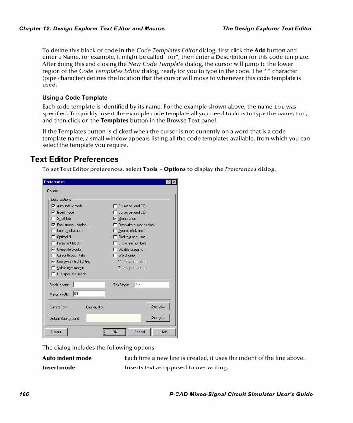
Chapter 12: Design Explorer Text Editor and Macros The Design Explorer Text Editor
166 P-CAD Mixed-Signal Circuit Simulator User’s Guide
To define this block of code in the Code Templates Editor dialog, first click the Add button and enter a Name, for example, it might be called “for”, then enter a Description for this code template. After doing this and closing the New Code Template dialog, the cursor will jump to the lower region of the Code Templates Editor dialog, ready for you to type in the code. The “|” character (pipe character) defines the location that the cursor will move to whenever this code template is used.
Using a Code Template Each code template is identified by its name. For the example shown above, the name for was specified. To quickly insert the example code template all you need to do is to type the name, for, and then click on the Templates button in the Browse Text panel.
If the Templates button is clicked when the cursor is not currently on a word that is a code template name, a small window appears listing all the code templates available, from which you can select the template you require.
Text Editor Preferences To set Text Editor preferences, select Tools » Options to display the Preferences dialog.
The dialog includes the following options:
Auto indent mode Each time a new line is created, it uses the indent of the line above.
Insert mode Inserts text as opposed to overwriting.

The Design Explorer Text Editor Chapter 12: Design Explorer Text Editor and Macros
P-CAD Mixed-Signal Circuit Simulator User’s Guide 167
Smart tab Tabs to the spaces in the previous line(s). This feature is disabled if the Use Tab Character option is enabled.
Backspace unindents With this option backspace unindents text to the previous indent level, using either the tab stops or the spaces in the line(s) above according to the Smart Tab option.
Use tab character With this option off, spaces are used instead of tabs and the Smart Tab feature is disabled.
Optimal fill This option works in conjunction with the Use Tab Character option. When auto indenting, this option uses the minimum number of characters, i.e. it will optimize the number of tab characters and the number of space characters to use the lowest total number possible.
Persistent blocks This option makes selections persistent, i.e. each selection will persist until another selection is made.
Overwrite blocks When enabled, text that is entered while there is a selection replaces the selection.
Cursor through tabs When unselected, tab characters appear like spaces.
Use syntax highlighting When unselected, the current syntax highlighting scheme is ignored.
Visible right margin Shows/hides the right margin.
Use special symbols Shows/hides end of line and end of file symbols.
Cursor beyond EOL When unselected, you cannot position the cursor beyond each line’s end. Instead the cursor will jump to the end of the line or to the previous/next line.
Cursor beyond EOF When unselected, the user cannot position the cursor beyond the End Of File. Also line numbers are only displayed up to the last line.
Group undo With this option selected, performing an undo will undo all previous operations of the same type, as opposed to a single operation.
Overwrite cursor as block With this option on, the cursor changes to a block when “insert mode” is off.
Double click line With this option, a double click will highlight the clicked line, as opposed to the clicked word.
Find text at cursor With this option on, when you select Edit » Find from the menus, the Find dialog will open with the word currently under the cursor entered in the Text to Find field.
Show line numbers Shows/hides line numbers on the left of the Text Editor window.

Chapter 12: Design Explorer Text Editor and Macros The Design Explorer Text Editor
168 P-CAD Mixed-Signal Circuit Simulator User’s Guide
Disable dragging With this option on, text cannot be dragged and dropped from one location in the document to another. With this option off, text can be dragged and dropped, which means that selections cannot be made by dragging the cursor.
Word wrap Specifies whether lines are wrapped and where they are wrapped.
Block indent Specifies how many characters each indent/unindent operation indents text by.
Margin width Specifies where the right margin is drawn.
Tab stops Specifies the tab stops to use. The difference between the last two tab stops is used to work out the trailing tab stops, e.g. if 4, 7 is specified, the tab stops are 4, 7, 10, 13, 16, etc.
Finding text You can find text in the Text Editor by choosing Edit » Find from the menus, or by clicking on the Browse Text tab, typing the required text into the Find field and clicking Search.
If you choose Edit » Find, the Find Text dialog includes the following options:
Case sensitive Text is only found when all characters have the same case as the string in the Text to find field.
Whole words only Text is only found when the string is preceded by a space and followed by a non-alpha or non-numeric character (e.g. #, %, !, etc).

The Design Explorer Text Editor Chapter 12: Design Explorer Text Editor and Macros
P-CAD Mixed-Signal Circuit Simulator User’s Guide 169
Regular expressions Regular expressions are characters that are used to customize the search string. Valid regular expressions include the following characters:
Character Description
^ A caret at the start of the string instructs the Find command to only match when the string is at the start of a line.
$ This character at the end of the string instructs the Find command to only match when the string is at the end of a line.
. A period indicates any single character. For example te.t matches test, tent but not tet.
* An asterisk indicates any set of characters, including no characters. For example, te* matches text, tent, te, but not t.
+ A plus sign indicates any set of characters, except no characters. For example, te+ matches text, tent, but not te.
[ ] Find any of the characters enclosed in the brackets.
[^] A caret at the start of a string in brackets means NOT. For example, [^tes] matches any characters except t, e, or s.
[-] A hyphen within a string in brackets signifies a range of characters. For example, [l-o] matches the characters l, m, n, and o.
{ } Braces are used to group characters or expressions. Groups can be nested, with a maximum number of 10 groups in a single pattern.
\ A backslash before a wildcard character tells the Text Editor to treat that character literally, not as a wildcard. For example, \^test does not look for the string test at the start of a line, it looks for the string ^test.
Direction Specifies that the search is to be done in a top-down direction, or bottom-up
direction. This works in conjunction with the current Origin setting, if the Origin is set to Entire scope then the search is either from the top of the document if the direction is set to Forward, or from the end of the document if the direction set to Backward.
Scope The search can be limited to the selected text, or can include all text.
Origin The search can either start from the current cursor position (From cursor), or from the beginning of the document (Entire scope).
If you search for text using the Browse Text tab, the line numbers and filename of all occurrences of the nominated text string will display. Click on a line to see it highlighted in the Text Editor window.
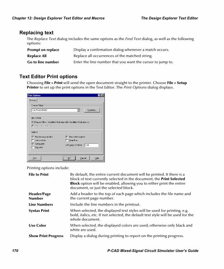
Chapter 12: Design Explorer Text Editor and Macros The Design Explorer Text Editor
170 P-CAD Mixed-Signal Circuit Simulator User’s Guide
Replacing text The Replace Text dialog includes the same options as the Find Text dialog, as well as the following options:
Prompt on replace Display a confirmation dialog whenever a match occurs.
Replace All Replace all occurrences of the matched string.
Go to line number Enter the line number that you want the cursor to jump to.
Text Editor Print options Choosing File » Print will send the open document straight to the printer. Choose File » Setup Printer to set up the print options in the Text Editor. The Print Options dialog displays.
Printing options include:
File to Print By default, the entire current document will be printed. It there is a block of text currently selected in the document, the Print Selected Block option will be enabled, allowing you to either print the entire document, or just the selected block.
Header/Page Number
Add a header to the top of each page which includes the file name and the current page number.
Line Numbers Include the line numbers in the printout.
Syntax Print When selected, the displayed text styles will be used for printing, e.g. bold, italics, etc. If not selected, the default text style will be used for the whole document.
Use Color When selected, the displayed colors are used; otherwise only black and white are used.
Show Print Progress Display a dialog during printing to report on the printing progress.

Macros Chapter 12: Design Explorer Text Editor and Macros
P-CAD Mixed-Signal Circuit Simulator User’s Guide 171
Wrap Lines Automatically wrap lines to fit the page.
Left Margin Sets the distance from the left edge of the paper to the left edge of the printed text.
Macros The Design Explorer includes a Macro server. The Macro server supports the Client Basic scripting language, which is a subset of Visual Basic™.
Macros provide a powerful mechanism to enhance your productivity. The macro server supports all the processes available in the Design Explorer environment, and allows passing of parameters to those processes. Macros can be written to work with any server running in the Design Explorer and must be saved with a .bas extension. Example scripts are in the \Design Explorer 99 SE\System\Templates.ddb design database.
Macros can perform anything from a repetitive sequence of processes, through to complex wizards which pop up dialog boxes and respond to user choices. The macro server also supports OLE automation, a feature where operations can be performed in other Windows applications that also support OLE automation.
Client Basic is interpreted rather than compiled, so macros can be run as soon as they are written. Like all processes in the Design Explorer environment, macros can be launched from a menu, toolbar button or a shortcut key. Client Basic includes a set of debugging tools which support breakpoints, variable watching, single step and real-time animation, where the macro is run at a slow enough speed to watch the code being executed. Choose View » Toolbars » Macro Debug Tools to show these tools.
While macro scripts can be written using any text editor, Design Explorer 99 SE's in-built text editor includes extensive features to make macro creation easier, such as Client Basic syntax highlighting.
Creating a new macro To create a new macro script using Design Explorer 's in-built Text Editor:
1. Select File » New from the menus, and choose Text from the list.
2. With the blank text document active in the text Editor window, select Tools » Change Language from the menus and choose Basic from the list. This will enable syntax highlighting.
3. Create your macro using the functions and statements of the Client Basic language. The options in the Macros menu will assist you.
4. Select File » Save As from the menus. Name the file and choose Client Basic Macro Script (*.bas) in the Save as Type field.

Chapter 12: Design Explorer Text Editor and Macros Macros
172 P-CAD Mixed-Signal Circuit Simulator User’s Guide
For comprehensive information on how to write macros in Client Basic, as well as example code, refer to the On-line Help system.
Manually running a macro To run a script, it must be stored in a design database. To manually run a script, select Run Script from the System menu located at the far left of the Design Explorer menus. The Select dialog will appear. If the macro is stored in the active design database, you can browse to locate it. If it is stored in a design database that is not currently open, press the Add button. Locate the design database in the Open dialog, and double-click to add it. Browse to locate the macro, select it and click on the OK button at the bottom of the Select dialog to run the macro.
When a macro is run, the macro server interprets the script. According to the script, it may pop up dialog boxes, make calls to other applications via OLE automation, or invoke processes and pass process parameters directly to one of the Design Explorer editors.
Error highlighting The Macro server includes a comprehensive error flagging mechanism. When an error is encountered, the script file is opened in the Text Editor, the line in error is displayed and highlighted, and a dialog pops up with a description of the error condition.
P-CAD Mixed-Signal Circuit Simulator User’s Guide 173
Index
-A- AC analysis
setting up and running.............................24 advanced simulation options.....................99 Analog options and SPICE variables.........99 analog simulation, definition .......................3 Analyses Setup dialog..................................14 analyses, setting up the circuit simulator 17 Attributes........................................................87
-B- BJTs ..................................................................77
-C- Capacitors.......................................................75 circuit nodes ..................................................44 circuit simulator features ..............................1 CMOS logic components ...........................85 Code Templates ..........................................165 Collect Data For ......................................20, 21 compiling SimCode....................................111 components...................................................73
selecting simulation-ready ......................73 Constant (DC) simulation sources............57 creating digital simulation models .........107 Crystals............................................................83 Current sources ............................................57
-D- data points
displaying ....................................................53 Database, Design ............................................7 DC Sweep analysis
setting up and running.............................26 debug
SimCode....................................................118
Defining points..............................................14 dependent sources.........................................4 Design Database
definition .......................................................7 folders ..........................................................11 managing documents ...............................11
Design Explorer about...............................................................6 features ..........................................................5 getting started...............................................5 Macro server ............................................ 171 Navigation Panel ......................................6, 8 Servers and DLLs..........................................6 Text Editor................................................. 159
Design Explorer Text Editor code templates ........................................ 165 finding text ............................................... 168 languages.................................................. 160 preferences .............................................. 166 print options ............................................ 170 replacing text ........................................... 170 syntax highlighting ................................. 161
Design Window...............................................6 Editing view .................................................10 Folder view....................................................9 splitting ........................................................10
device descriptions.......................................74 digital designs
simulating ................................................. 107 Digital SimCode .......................See SimCode digital simulation model example.......... 111 digital simulation parts
creating symbols for............................... 108 defining property fields......................... 108 model linking file.................................... 109
Diodes .............................................................76 displaying waveforms...................................48
Index
174 P-CAD Mixed-Signal Circuit Simulator User’s Guide
-E- error file (.err) ............................. 14, 19, 20, 95 example circuits ............................................13 Exponential sources .....................................64 Exponential Waveform definition .............65
-F- F/V Converter source ...................................70 FM Waveform definition .............................68 Fourier analysis
setting up and running.............................36 frequency and phase, viewing ...................51 Frequency Modulation sources.................66 Fuses ................................................................83
-I- Impedance Plot analysis
setting up and running.............................39 Inductors.........................................................76 initial conditions
enabling .......................................................23 setting...........................................................44
installation and setup.....................................2 installing P-CAD products .........................2 system requirements ..................................2
-J- JFETs .................................................................78
-L- language syntax
SimCode ....................................................118 libraries ........................................ 3, 73, 87, 107 Library Index spreadsheet ..........................87 linear dependent sources .......................4, 68
-M- macros ...........................................................171 mathematical functions & waveforms......40 measurement cursors ..................................54 MESFETs ..........................................................80 model linking file for a digital simulation part .................................................................109 models.............................................................73
subcircuits ...................................................74 Monte Carlo analysis
Default distribution...................................30
Default tolerances..................................... 31 setting up and running ............................ 29 Simulation seed......................................... 30 Specific Device Tolerances..................... 31
MOSFETs ........................................................ 78 multi-pass results, interpreting ................. 55
-N- Noise analysis
setting up and running ............................ 38 non-linear dependent sources.............. 4, 69
-O- Operating Point analysis
setting up and running ............................ 28
-P- Parameter Sweep analysis
setting up and running ............................ 33 Periodic Pulse source .................................. 60 Piece-Wise-Linear source........................... 62 Pulse Shape definition ................................ 61
-R- Relays .............................................................. 84 Resistors ......................................................... 74 Run Analyses ................................................. 14 Run simulation.............................................. 14
from Circuit Simulator ............................. 19 from the Schematic design ..................... 18
-S- scaling
waveform axes ........................................... 52 waveforms .................................................. 48
Schematic Editor................................. 3, 17, 40 selecting analyses to run ............................ 22 selecting simulation-ready components. 73 setting up
AC analysis.................................................. 24 advanced simulation options ................. 99 DC Sweep analysis.................................... 26 Fourier analysis.......................................... 36 Impedance Plot analysis .......................... 39 Monte Carlo analysis................................ 29 Noise analysis ............................................ 38 Operating Point analysis ......................... 28 Parameter Sweep analysis....................... 33
Index
P-CAD Mixed-Signal Circuit Simulator User’s Guide 175
simulation analyses ...................................17 Temperature Sweep analysis ..................35 Transfer Function analysis.......................37 Transient analysis ......................................22
Setting up the Analyses ...............................14 SimCode ...................................4, 107, 131, 142
beginning a model definition...............115 compiling ..................................................111 function in model file.............................111 including comments...............................115 language definition.................................115 Language Reference ...............................114 language syntax .......................................118 statement termination character .........114
SimCode devices creating new .............................................107
SimCode digital device simulation model creating a ...................................................111 example file ..............................................111
SimDefaults....................................................93 SimFile.............................................................90 Simlist.TXT file .............................................111 SimModel .......................................................89 SimNetlist .......................................................91 SimPins............................................................90 SimType ..........................................................87 simulation
compiling a SimCode model ................111 creating digital simulation models ......107 displaying data points...............................53 displaying waveforms...............................48 getting started ............................................13 identifying circuit nodes..........................44 interpreting multi-pass results ...............55 limits ...............................................................4 mathematical functions & waveforms ...4,
40 model support..............................................4 setting up and running.............................17 SimCode language definition...............115 sources...................................... See Sources using measurement cursors....................54 viewing frequency and phase.................51
simulation attributes SimDefaults.................................................93 SimField1-16................................................93 SimFile..........................................................90
SimModel ....................................................89 SimNetlist ....................................................91 SimPins.........................................................90 SimType .......................................................87
simulation configuration file (.cfg)............17 simulation data
specifying.....................................................20 to be collected............................................20 to be displayed ...........................................21
Simulation Data File (.sdf) .............................5 simulation digital designs simulation problems ....................................95
analysis failures ..........................................96 DC Sweep analysis.....................................97 general simulation convergence............96 netlist cannot be created .........................95 Transient analysis.......................................98
simulation results window..........................47 Simulation Source library............................57 simulation-ready components
creating your own......................................87 TTL and CMOS logic components.........85
simulation-ready integrated components...........................................................................85 simulation-ready symbols .............................3
BJTs................................................................77 Capacitors....................................................75 Crystals.........................................................83 Diodes ..........................................................76 Fuses .............................................................83 Inductors .....................................................76 JFETs ..............................................................78 MESFETs .......................................................80 MOSFETs......................................................78 Relays............................................................84 Resistors.......................................................74 Transformers...............................................83 Transmission Lines ....................................81 V/I Controlled Switches............................80
SimView Setup...............................................21 Sine Wave definition....................................59 Sinusoidal source..........................................58 Smart Technology ...........................................6 source components......................................14 sources
Constant (DC).............................................57 Exponential..................................................64

Index
176 P-CAD Mixed-Signal Circuit Simulator User’s Guide
F/V Converter..............................................70 Frequency Modulation.............................66 Linear Dependent......................................68 Non-linear Dependent .............................69 Periodic Pulse .............................................60 Piece-Wise-Linear ......................................62 Sinusoidal ....................................................58 VCO ..............................................................71
SPICE compatibility .................................................4 suggested reading ...................................104
SPICE netlist .............................................18, 19 filename (.nsx) ..............................................5 modifying ....................................................43
SPICE variables and Analog options .........99 STEP_OFF ......................................................118 STEP_ON.......................................................118 subcircuits ......................................................74 Symbol Editor.................................................87 Syntax Editor ................................................161 syntax highlighting .....................................161 system requirements .....................................2
-T- Temperature Sweep analysis
setting up and running.............................35 Text Editor.....................................................159
code templates.........................................165 finding text ................................................168 languages...................................................160 preferences ...............................................166 print options .............................................170 replacing text ............................................170 syntax highlighting ..................................161
Transfer Function analysis setting up and running ............................ 37
Transformers ................................................. 83 Transient analysis
setting up and running ............................ 22 Transmission Lines....................................... 81 troubleshooting simulation problems .... 95 TTL logic components................................. 85
-U- Use Initial Conditions ................................. 23
-V- V/I Controlled Switches .............................. 80 VCO source ................................................... 71 viewing simulation results ......................... 15 voltage and current sources ...................... 57
-W- Waveform Analysis window....................... 19
using............................................................. 47 waveform functions & operators.............. 42 waveforms
displaying.................................................... 48 displaying data points .............................. 53 displaying together................................... 51 identifying................................................... 53 scaling.......................................................... 48 single cell, all cells .................................... 50 using measurement cursors ................... 54
-X- XSpice ....................................................... 18, 19