micro-electromechanical systems for nano-science
TRANSCRIPT

Journal of Nanoparticle Research2: 413–418, 2000.© 2000Kluwer Academic Publishers. Printed in the Netherlands.
Micro-electromechanical systems for nanoscience
U. Staufer, T. Akiyama, C. Beuret, S. Gautsch, W. Noell, G. Schurmann, C. Stebler∗ and N.F. de RooijInstitute of Microtechnology, University of Neuchˆatel, Jaquet-Droz 1, 2007 Neuchˆatel, Switzerland(Tel.:+ 41 32 720 5357; Fax:+ 41 32 720 5711; E-mail: [email protected])∗New address: ETEC Systems INC, 26460 Corporate Avenue, Hayward, CA 94545, USA
Received 15 July 2000; accepted 23 October 2000
Key words:MEMS, scanning probe microscopy, electron-beam lithography, dust particles, space applications
Abstract
Micro-electromechanical systems are ideal tools for nanoscience because they bridge the gap between the nano- andthe macro-world. Moreover, several of these instruments can be operated in parallel to either increase the throughputor to provide redundancy. The majority of the components of such a system have dimensions above the nanometerscale. Still, some require placement and pattern accuracy well below this limit. This will be highlighted in a shortreview of a few examples: Scanning optical near field microscope probe fabrication, where an aperture of 50 nmin diameter was incorporated at the probing tip; parallel scanning force microscope for measuring dust particleson Mars where redundancy is essential; and a miniaturized electron column for parallel electron beam lithography,where the throughput needs to be increased.
Introduction
Micro-electromechanical systems (MEMS) have typi-cal dimensions from a few microns up to the millimeterrange. Yet they are attractive for nano-science becausethey provide an interface from the macro- to the nano-world due to their mesoscopic size. Their reducedsize compared to macroscopic instruments is essen-tial because different properties of a device scaledifferently upon miniaturization. Therefore, e.g. micro-fabricated springs can have a very high resonancefrequency while being very soft and, hence, allowingto measure small forces even in a noisy environment.Also the well developed transducer concepts of themicrosystem technology (MST) are suited for mea-suring the desired parameters of the nano-object. Agood example for illustrating this are the piezoresitivecantilevers which have been developed for measuringminute forces in the scanning force microscopy (AFM)(Tortonese et al., 1993).
The MEMS itself can also have a nanometer sizedcomponent, e.g. a sharp tip in the case of the scan-ning probe microscopes (SXM) where a high spatialresolution is required. The tip limits the interactionbetween the sensor and the sample to a small area,thus providing a kind of ‘focus’. Also the placementof components or their micrometer size dimensionsmust sometimes be precise to a few nanometers. Agood example is the Millipede storage device of IBM(Vettiger et al., 1999) where a whole array of 32× 32cantilevers with small tips (1.5µm height, 20 nm radiusof curvature) are used to write pits 40 nm in size intoa polymer. The fabrication of this device needs inmany processing steps a precision in the range of afew 10 nm. But for many other applications the MEMSstays in the micrometer range. Examples are the nano-balances for thermogravimetry where small changesin the mass of a substance is measured as function ofthe temperature (Berger et al., 1998). Similarly, chem-ical reactions between a few molecules can be detected

414
by measuring small temperature changes by meansof a micro-fabricated bimorph beam (Gimzewskiet al., 1994). Conventional transducers like stress-or temperature-dependant resistors, position-sensitivephoton detectors, or capacitive position sensors areused for measuring the required quantity in the majorityof these cases. Only a few concepts employ or fore-see to employ size dependant quantum effects likeelectron tunneling or coulomb blockade, or to use,e.g. an individual (macro-)molecule as detector oractuator. In those cases, one could also speak ofnano-electromechanical systems or NEMS.
Micro-fabricated microscopes
Among the different tools for nano-science, thosewhich directly generate a two or three dimensionalimage of the nano-object have a prominent positionsince such pictures are appealing to the intuition ofthe researcher and his desire of modeling the object.These instruments can be divided into far and near-fieldmicroscopes.
Scanning near-field optical microscope
The scanning near-field optical microscope (SNOM orNSOM) is one of the areas where micro-system tech-nology can still contribute a lot to the development.SNOM was invented by D.P. Pohl et al. (1984) andsoon gained a lot of attention because of its potential toadd spectral measurements to the spatial ones, hence,allowing to gain chemical information. The key ele-ment in SNOM is the probing tip which guides the lighteither to or from the sample. In order to limit the inter-action to a very small volume, the near-field region,the tip features a tiny metal aperture at its apex. Wefound that such apertures can be machined on micro-fabricated tips in a relatively easy way (Schurmannet al., 1999). The tip is coated first with an aluminumfilm, the usual metal used in most SNOM probes forits optical properties. The aluminum has a thicknessof about 50 nm. Then, SixNy 100 nm thick is added byplasma enhanced chemical vapor deposition (PECVD).This SixNy film showed a enhanced etch rate at the tipapex when attacked by reactive ion etching (RIE) in afluorine- and chlorine-based plasma. We explain thisby the field enhancement due to the high curvature atthe tip which accelerates the ions to the apex. A care-fully timed RIE will, therefore, form a small opening
Figure 1. Scanning electron microscope image of SNOM pn-junction tip featuring a 50 nm diameter aperture in the aluminumcoating.
in the SixNy film which we then use as a mask for wet-chemically etching the aluminum coating. In Figure 1an example of such an aperture on a silicon tip is shown.Typical diameters are in the range from 50 to 70 nm.The silicon tip underneath the aluminum aperture con-tains a pn-junction and can be used as photodiode. Wefabricated such tips also on AFM cantilevers and usedthem for imaging the light emitting facet of a laserdiode (Schurmann et al., 2000). Of course, our tech-nique of aperture fabrication is difficult to transfer tothe glass-fiber tips which are more common in SNOMset-ups. We started therefore to also micro-fabricatequartz tips out of quartz wafers as a first step towards aconcept which foresees quartz tips added onto siliconAFM cantilevers.
Scanning force microscope for experiments on Mars
The following project makes use of another aspect ofMEMS. The small size of the components allows toalign several of them in a row or an array. This allows tohave some redundancy in instruments which are oper-ated at remote or hardly accessible areas. An exampleis our space AFM.
The interplanetary research plan of NASA includesmanned Mars Missions in the beginning of this century.The red planet may see the arrival of the first astro-nauts in the late tens or early twenties of this centuryeven with the recent problems encountered with theunmanned lander missions. Such human exploratoryand discovery missions require, of course, a carefulassessment of potential hazards on our neighbor planet.
415
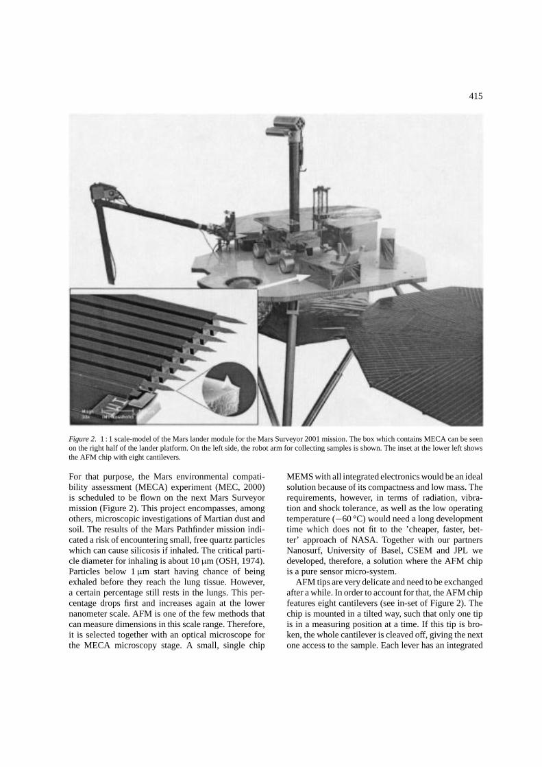
Figure 2. 1 : 1 scale-model of the Mars lander module for the Mars Surveyor 2001 mission. The box which contains MECA can be seenon the right half of the lander platform. On the left side, the robot arm for collecting samples is shown. The inset at the lower left showsthe AFM chip with eight cantilevers.
For that purpose, the Mars environmental compati-bility assessment (MECA) experiment (MEC, 2000)is scheduled to be flown on the next Mars Surveyormission (Figure 2). This project encompasses, amongothers, microscopic investigations of Martian dust andsoil. The results of the Mars Pathfinder mission indi-cated a risk of encountering small, free quartz particleswhich can cause silicosis if inhaled. The critical parti-cle diameter for inhaling is about 10µm (OSH, 1974).Particles below 1µm start having chance of beingexhaled before they reach the lung tissue. However,a certain percentage still rests in the lungs. This per-centage drops first and increases again at the lowernanometer scale. AFM is one of the few methods thatcan measure dimensions in this scale range. Therefore,it is selected together with an optical microscope forthe MECA microscopy stage. A small, single chip
MEMS with all integrated electronics would be an idealsolution because of its compactness and low mass. Therequirements, however, in terms of radiation, vibra-tion and shock tolerance, as well as the low operatingtemperature (−60 °C) would need a long developmenttime which does not fit to the ’cheaper, faster, bet-ter’ approach of NASA. Together with our partnersNanosurf, University of Basel, CSEM and JPL wedeveloped, therefore, a solution where the AFM chipis a pure sensor micro-system.
AFM tips are very delicate and need to be exchangedafter a while. In order to account for that, the AFM chipfeatures eight cantilevers (see in-set of Figure 2). Thechip is mounted in a tilted way, such that only one tipis in a measuring position at a time. If this tip is bro-ken, the whole cantilever is cleaved off, giving the nextone access to the sample. Each lever has an integrated

416
Forward Scan
Zou
tput
: 0.8
63µm
0µm
Yx
27.2
µm
0 µm Xx 27.2 µm
Figure 3. Raw data AFM image of a 10µm pitch calibration grid,recorded with the space AFM.
piezoresistor as deflection sensor which can be indi-vidually addressed from the controller electronics bymeans of a multiplexer. Four out of the eight tips arediamond pyramids. Their hardness should increase thelife-time. The substrates, on to which the dust and soilsamples will be deposited by means of a robot arm,are made of technologically important materials likespace suits. Besides that, also calibration samples willbe available. Figure 3 shows an AFM image of such atwo dimensional 10µm grid.
Miniaturized electron beam writer
Parallel operation of micro-fabricated instruments doesnot only provide redundancy but can also increasethroughput if all devices are simultaneously run. Thistime, the small size is important in order to increasethe density of the instruments. One example is theminiaturized e-beam writer, an instrument intended tobe used for direct write e-beam lithography (EBL) inthe sub 100 nm range. It is based on a concept, thatwas introduced by T.H.P. Chang et al. a few years ago(Chang et al., 1989; Stebler et al., 1996a,b).
Heart of the e-beam writer is the micro-column. Asshown in a theoretical study, its performance shouldsurpass the one of a conventional column working atthe same energy (Chang et al., 1989) due to the reduceddimensions, however only if the relative fabrication tol-erances can be maintained! The bore hole in a classicalelectron lens is in the order of a millimeter and theprecision of the roundness and the edge roughness is
xy Sample Stage
Einzel Lens
Double OctupoleDeflection Unit
Source Lens
CFE Electron Source
xyz Friction Walkerwith Piezo Tube Scanner
3 m
m1
mm
Figure 4. Set-up of the electron micro-column. CFE stands forcold field emission.
between 1 and 10µm. Reducing the bore hole to about1µm implies, hence, a precision of 1–10 nm!
The micro-column is an example of a three dimen-sional hybrid MEMS. A sketch of the configuration ofthe e-beam writer is shown in Figure 4. The electrostaticlenses are made of 1–2µm thick silicon membraneelectrodes and Pyrex spacers. The fabrication pro-cess which we have developed (Despont et al., 1995)is summarized in Figure 5. First, highly doped sili-con membranes are fabricated by anisotropic etching.Then, the bore hole (1–5µm) of the first electrode ismachined by means of EBL and reactive ion etching(RIE). In the next step, the 50µm thick Pyrex spacerand a second silicon membrane are simultaneouslybonded to the first electrode (Despont et al., 1996).Next, resist is spun on the backside of the second mem-brane. By carefully adjusting the energy of the e-beam,this resist can be exposed through the membrane, usingalignment marks in the first electrode as mask. A sec-ond EBL, which will define the second bore hole, andwhich is performed from the backside after a first devel-opment step, can be registered on these resist marks.An alignment accuracy of about 0.1–0.2µm of the sec-ond bore relative to the first one can be achieved withthis approach.
Deep reactive ion etching is used for fabricatingthe silicon deflector electrodes (Stebler et al., 1999).Here, the critical dimension and placement are lessproblematic but the control of the surface rough-ness of the sidewalls was important. In Figure 6an AFM image of one of the sidewalls is shown.The rms roughness-value after post-processing by

417
(a)
(b)
(c)
(d)
Figure 5. Process flow chart for the fabrication of an electro-static electron lens. (a) The center bore hole and at least twoalignment marks are machined into a silicon membrane by e-beamlithography and reactive ion etching. (b) A Pyrex spacer and asecond membrane are anodicaly bonded to the first electrode.Resist is spun on the back-side of the second membrane. (c) Theresist is exposed through the second membrane using the first oneas mask. (d) The resist masks are developed and the chip is againmounted to the e-beam writer. After registering to these marks,the bore of the second electrode is exposed.
Figure 6. AFM image (10µm × 10µm) of the end face of asilicon electrode which has been fabricated by deep reactive ionetching. The z range of the image is 186 nm and the rms roughnessvalue is 19 nm.
polishing with potassium hydroxide (40%, room tem-perature) amounted to 19 nm, which is acceptable forour application.
Summary and conclusion
Even if the critical dimension of a MEMS is in themicrometer range, its fabrication often needs to be con-trolled in the nanometer range, especially if it shouldbe used as a tool for nanoscience. The few examplepresented in this overview showed, that MEMS canbe used as interface to the nano-world and provide aninteresting set of tools for nano-science.
Acknowledgements
Parts of this work have been financial supported by theWolfermann Nageli Stiftung, the European ESPRITprogram, SPP Optique I and SPP MINAST whichare both programs of the Board of the Swiss FederalInstitutes of Technology, and by a collaboration withETEC Systems, Inc. We thank our collaborators fromother institutes for many helpfull discussions andacknowledge their contribution to this work: D. Lange,Ch. Hagleitner, O. Brand, A. Tonin, H.R. Hidber, L.

418
Howald, D. Muller, Ph. Niedermann, H. Heinzelmann,T.H.P. Chang, K. Lee, L.P. Muray. We also thank ourformer team members P.-F. Indermuhle, T. Pfeffer, D.Wylie for their work when they were still at IMT.
References
Berger R., Lang H.P., Gerber Ch., Gimzewski J.K., Fabian J.H.,Scandella L., Meyer E. & Guntherodt H.-J., 1998. Chem. Phys.Let. 294, 363.
Chang T.H.P., Kern D.P. & McCord M.A., 1989. J. Vac. Sci.Technol. B7 1855.
Despont M., Staufer U., Stebler C., Germann R. & Vettiger P.,1995. Microelectronic Eng. 27, 467.
Despont M., Gross H., Arrouy F., Stebler C. & Staufer U., 1996.Sensors and Actuators A55, 219.
Gimzewski J.-K., Gerber Ch., Meyer E. & Schlittler R.R., 1994.Chem Phys. Lett. 217, 589.
MEC, 2000. http://mars.jpl.nasa.gov/2001/lander/meca/OSH, 1974. OSHA Fact Sheet No. 96-54. http://www.osha-
slc.gov/SLTC/silicacrystalline/silicacriteria/Pohl D. W., Denk W. & Lanz M., 1984. Appl. Phys. Lett. 44,
651.Schurmann G., Indermuhle P.F., Staufer U. & de Rooij N.F., 1999.
Surf. Interface Anal. 27, 299.Schurmann G., Noell W., Staufer U. & de Rooij N.F., 2000.
Ultramicroscopy 82, 33.Stebler C., Despont M., Staufer U., Chang T.H.P., Lee K.Y. &
Rishton S.A., 1996. Microelectronic Eng. 30, 45.Stebler C., Despont M. & Staufer U., 1996. J. Phys III France 6,
1435.Stebler C., Pfeffer T., Staufer U. & de Rooij N.F., 1999.
Microelectronic Eng. 46, 401.Tortonese M., Barett R.C. & Quate C.F., 1993. Appl. Phys. Lett.
62, 834.Vettiger P., Brugger J., Despont M., Drechsler U., Durig U.,
Haberle W., Lutwyche M., Rothuizen H., Stutz R., Widmer R.& Binnig G., 1999. Microelectronic Eng. 46, 11–17.