metal blacks as scattering centers to increase the efficiency …rep/theses/deep_ms_2011.pdf ·...
TRANSCRIPT

METAL BLACKS AS SCATTERING CENTERS
TO INCREASE THE EFFICIENCY OF THIN FILM SOLAR CELLS
by
DEEP R. PANJWANI
M.Sc. M.S. University of Baroda, 2008
B.Sc. M.S. University of Baroda, 2006
A thesis submitted in partial fulfillment of the requirements
for the degree of Master of Science
in the Department of Physics
in the College of Sciences
at the University of Central Florida
Orlando, Florida
Summer Term
2011
Major Professor: Robert E. Peale

ii
ABSTRACT
Metal nano particles are investigated as scattering centers on front surface of thin-film solar cells
to improve efficiency. The principle is that scattering, which is enhanced near the plasmon
resonance frequency of the particle and depends on particle size, increases the effective optical
path length of incident light, leading to more light absorption in active layer of thin film solar
cell. The particular types of particles investigated here are known as “metal-black”, well known
as an IR absorber for bolometric infrared detectors. Gold-black was deposited on commercial
thin-film solar cells using a thermal evaporator in a nitrogen ambient at pressures of ~1 Torr. We
suggest that the broad range of length scales for gold black particles, as quantified by scanning
electron microscopy, gives rise to efficient scattering over a broad range of wavelengths across
the solar spectrum. The solar cell efficiency was determined both as a function of wavelength
and for a solar spectrum produced by a Xe lamp and appropriate filters. Up to 20% increase in
short-circuit photocurrent, and a 7% increase in efficiency at the maximum power point, were
observed.

iii
To my Parents

iv
ACKNOWLEDGMENTS
My sincerely thanks to my advisor Dr. Robert Peale, without his help and guidance, this project
could never have been accomplished. It is my honor to be part of the group led by him.
I really appreciate Mr. Chris J. Fredricksen for his invaluable help preparing experimental setup
and being there during any troubleshoot periods to keep the project on the course. I am not able
to appreciate his help more, but working with him was a great learning experience. Dr. Ken
Beck & Alan Joly from EMSL lab provided electrodynamic simulation for this project and
support for the PEEM measurements, I earnestly value their help.
I am grateful to Dr. Aniket Bhattacharya & Dr. Masahiro Ishigami for being on my dissertation
committee and evaluating this project.
I wish to thank to all my group members, Janardan Nath, Farnood Khalilzadeh Rezaie, Gautam
Medhi, Evan Smith, Tataiana Brusentsova, Pedro Figueiredo, Monas Shahzad Nima Nader,
Hajrah Qudusi, Lin Yuqin and Yauheni Rudzevich.
The authors were supported by the Department of Energy, Office of Basic Energy Sciences,
Division of Chemical Sciences, Geosciences, and Biosciences; Pacific Northwest National
Laboratory (PNNL) is operated for the U.S. Department of Energy by Battelle. This research was

v
performed using the EMSL, a national scientific user facility sponsored by the Department of
Energy's Office of Biological and Environmental Research and located at PNNL.

vi
TABLES OF CONTENTS
LIST OF FIGURES ..................................................................................................................... viii
LIST OF TABLES ......................................................................................................................... xi
INTRODUCTION .......................................................................................................................... 1
CHAPTER ONE: SOLAR CELL ................................................................................................... 4
1.1 Photoelectric Effect ............................................................................................................... 4
1.2 Solar radiation ....................................................................................................................... 5
1.3 Ideal conversion efficiency of solar cell ............................................................................... 6
1.4 Thin film solar cell ................................................................................................................ 9
CHAPTER TWO: PLASMONIC NANO STRUCTURES IN PHOTO VOLTAICS ................. 14
2.1 Plasmonic nano structures as scattering centers ................................................................. 14
2.2 Localized Surface Plasmons ............................................................................................... 16
2.3 Lithographically produced ordered array of nano particles ................................................ 22
CHAPTER THREE: EXPERIMENT ........................................................................................... 25
3.1 Deposition of gold black thin film on solar cell ................................................................. 25
3.2 Characterization of Solar Cell ............................................................................................. 29
CHAPTER FOUR: RESULTS ..................................................................................................... 34
4.1 Measurements on Standard Thick Single Crystal Solar Cell .............................................. 34
4.2 Measurements on Thin Film Amorphous Silicon Solar Cell .............................................. 38
4.3 Optimization and Understanding ........................................................................................ 41
4.3.1 Percentage coverage & Wavelet Analysis ................................................................... 41
4.3.2 Photo Electron Emission Microscopy (PEEM) ........................................................... 43

vii
4.3.3 Simulation .................................................................................................................... 46
CHAPTER FIVE: CONCLUSION & SUMMERY ..................................................................... 51
LIST OF REFERENCES .............................................................................................................. 53

viii
LIST OF FIGURES
Figure 1 P-N Junction after equilibrium is attained ........................................................................ 4
Figure 2 Curve related to solar spectral irradiance for AM0 & AM1.5 [after Thekaekara, Ref.11]
......................................................................................................................................................... 5
Figure 3 Depiction of different air mass conditions ....................................................................... 6
Figure 4 (Left) Solar cell equivalent circuit. (Right) Energy diagram of p-n junction while
irradiated by solar flux. ................................................................................................................... 7
Figure 5 Current-Voltage characteristics of solar cell under illumination [After Prince, Ref 13]. 8
Figure 6 Optical transitions: (Left) indirect transition involving phonon. (Right) direct transition
in which, only photon excites electron from valance band to conduction band. .......................... 11
Figure 7 Absorption coefficients for a-Si is in range 104 to 10
5 cm
-1 in visible range of solar flux
[Ref, 15] ........................................................................................................................................ 12
Figure 8 Thin film solar cell is not able to harvest entire solar flux due to low absorption
coefficient value for „visible red‟ & „infrared‟ ............................................................................. 13
Figure 9 Employing metal scattering centers increases the optical path length of thin film solar
cell. ................................................................................................................................................ 15
Figure 10. Field intensity enhancement around 100 nm diameter silver cylinder on quartz
substrate illuminated with plane waves from above [Ref 16] ....................................................... 16
Figure 11 External electric field of incident light displaces the electron from its lattice ions which
results in oscillating electron density ............................................................................................ 17
Figure 12 Extinction coefficient as function of wavelength, 120 nm diameter particles show
dipole resonance at 430 nm and quadrupole resonance at 355 nm [from Reference 31]. ............ 21
Figure 13 Dependence of Plasmon resonance frequency on particle size and geometry [Ref, 18]
....................................................................................................................................................... 22
Figure 14 Extinction (solid lines) & Scattering (dashed lines) cross section for Ag nano particles
of 100 nm size on different embedding medium such as air(black), Si3N4(blue) and Si(red)
[reference 2]. It can be noticed that scattering cross section is enhanced in very limited region for
all the embedding mediums. ......................................................................................................... 23

ix
Figure 15. Gold Black deposition uses a thermal evaporation chamber back filled up to ~1 Torr
with N2. ......................................................................................................................................... 26
Figure 16 Response of photo-detector at the different locations on the spot formed with Xe lamp.
....................................................................................................................................................... 30
Figure 17 Photograph of solar cell characterization facility. ........................................................ 31
Figure 18 Schematic of the photocell characterization set up. Monochromated Xe arc lamp light
of calibrated intensity passes through a filter to remove harmonics and impinges on the solar cell,
whose IV curve is measured. ........................................................................................................ 31
Figure 19 Current is passed trhough Solar Cell and Voltage is measured load resistance different
load resistences. ............................................................................................................................ 32
Figure 20. IV curve, plotted with power vs. voltage (circles), for the PowerFilm solar cell. MPP
(maximum power point) occurs at the knee. ................................................................................. 32
Figure 21. (top) Spectral characterization of an optically-thick Si solar cell. The black curve is
the spectral response of the Si solar cell before deposition, and the red is the response after
coating. (bottom) Ratio of “after” to “before,” showing an increase in the near IR. The response
decreases less at longer wavelengths where the silicon absorption is less and scattering by the
small particles gives an increase in light harvesting, which compensates somewhat the decrease
caused by shadowing. ................................................................................................................... 35
Figure 22. Response surfaces for efficiency, plotted as a function of gold mass and pressure at
constant boat current (left) and as a function of gold mass and evaporation boat current at
constant pressure (right). ............................................................................................................... 36
Figure 23 Response surfaces for percent coverage at constant pressure. ..................................... 37
Figure 24 Response surfaces for percent coverage at constant current. ....................................... 38
Figure 25 Demonstration of photocurrent increase across the spectrum for thin film solar cell
coated with gold-black particles. Photocurrent was measured under zero applied voltage. ........ 39
Figure 26 IV and photo-power curves for PowerFilm amorphous silicon solar cell for solar
spectrum irradiance. Also indicated on the IV curve is the Maximum Power Point (MPP). The
maximum power point before deposition was 9.15 mW. After deposition, the maximum power
point increased by 7%. .................................................................................................................. 40
Figure 27. Gold black increases the efficiency by 5.1% ............................................................... 41

x
Figure 28. (left) SEM image of lightly coated substrate. Goldblack film run #18 (0.5 mg Au, 400
mTorr, 68A) from Table 1. (right) Histogram generated from this image. The fraction of
coverage by gold black was determined from the tail of the histogram that extends beyond ~100
on the brightness scale. ................................................................................................................. 42
Figure 29. SEM image and histogram of heavily coated sample. Sample 6x (run #12 – 1.5 mg
Au, 1000 mTorr, 68 A). ................................................................................................................ 42
Figure 30. Results of wavelet analysis for the image in Fig. 27. ................................................. 43
Figure 31. SEM image (left) of a gold black sample. PEEM image of the same sample under Hg
lamp illumination (right). The field of view is 150 microns. ....................................................... 45
Figure 32. Gold black sample illuminated by a laser at two different wavelengths. (left) = 370
nm and (right) = 420 nm. .......................................................................................................... 45
Figure 33. Left: PEEM image of gold black film under = 370 nm laser illumination. Right:
under = 420 nm laser illumination. ............................................................................................ 46
Figure 34 The model system for Electrodynamic simulation using Lumerical. A layer of 100 nm
gold spheres is located 100 nm in front of the surface of a 200 nm thick silicon wafer. Radiation
is incident from outside the wafer (purple arrow). Blue arrows indicate the polarization and the
grey boxes define volume in which the radiation is confined. ..................................................... 47
Figure 35. A monitor at the surface of the silicon wafer, showing the spatial profile of the
intensity of the radiation. The highest intensity is shown in red. ................................................ 48
Figure 36. A monitor in the plane through the center of the layer of gold particles. High intensity
is seen around the edges of the gold spheres and none is seen inside the metal, as expected. ..... 49
Figure 37 A monitor 100 nm inside the silicon surface. The red regions show the very high
intensity enhancement due to the gold nanoparticles. .................................................................. 50

xi
LIST OF TABLES
Table 1 Two-level full factorial protocol and order of experiments ............................................. 29

1
INTRODUCTION
We are in the era when low cost, environment friendly, renewable energy sources are necessary
to comply with the demand of rapidly growing world population. Photo Voltaic Technology has
this capability since the amount of radiation from sun striking the Earth‟s surface is very high
compared to the energy usage of the entire planet and it is virtually pollution free. In order for
this technology to reliably solve future energy crisis, the cost of the electricity produced must
become comparable to the retail price of conventional electricity.
At the present the major portion of the solar-cell market is based on crystalline silicon with
thickness between 180-300 µm. This is much thicker than the characteristic absorption length for
solar photons in silicon (several microns), so that materials costs and weight are proportionally
high. Thin film solar cells promise to reduce costs. Thicknesses of 1-2 µm can be deposited on
cheap substrates such as plastic. Thin film solar cells can be made with different materials such
as a-Si, GaAs and CdTe as well as organic semiconductors [1]
. However, when the absorber
material becomes very thin, it may become partially transparent and incapable of harvesting the
entire solar flux. Therefore engineering solar cells in such a way that light trapping becomes
much more efficient is very important.
This work investigates the additional light trapping that occurs when small metal particles, in the
form of “gold-black”, are deposited as scattering centers on the front surface of thin film solar
cells. This increases the optical path length of incident light in absorber layer, increasing the
fraction of the incident flux that is absorbed.

2
Investigation of the increased effective path length within the absorber layers of such cells by
deposition of small metal scattering centers is being pursued by many groups. Lithographically
produced self-assembled arrays of metal dots have been shown to increase solar cell efficiency,
at least in part of the solar spectrum depending on geometry and size of deposited nano
particles[2]
. We investigated the possibility of using sparse depositions of gold black, a nano-
structured metal formed by a thermal evaporator with ~1 Torr inert ambient, giving a broad
distribution of particle sizes[3-7]
. The hypothesis is that the range of length scales inherent in
such depositions will provide spectrally broad scattering to provide efficiency enhancements
across the entire solar spectrum.
This report is organized as follows. The first chapter presents solar-cell physics and performance
parameters. The second chapter reviews localized surface plasmons in nano structures and how
the lead to the scattering of light that enhances efficiency of thin film solar cells. The
experimental section describes the deposition of gold black and the characterization process of
Power Film thin film solar cell. The results section presents a full factorial experiment performed
on standard crystal solar cell, which was performed mainly as an exercise to develop processing,
characterization, and analysis procedures, since efficiency improvements for thick cells are not
expected and were not observed. First results for thin film solar cells are presented and reveal
promising improvements in measured IV and photo-current response. Potential use of Photo
Emission Electron Microscopy (PEEM) is discussed to discover spatial and spectral dependence
of local field enhancement due to plasma resonances. Particle size distribution is determined by

3
wavelet analysis and percentage coverage is quantified by analysis of SEM histrograms. These
properties are to be correlated with deposition conditions and resulting efficiency changes. The
results section also includes an example of electrodynamic simulation for a thin silicon substrate
with gold particle over layer to study scattering and electric field enhancement. Finally, an
overview of the experimental results and analysis is given in the conclusion section.

4
CHAPTER ONE: SOLAR CELL
1.1 Photoelectric Effect
Solar cells convert light into electricity directly through photovoltaic effect. The light generates
electron-hole pairs in a diode structure, and these are separated by the built-in electric field to
produce a voltage. When the cell is connected to a load, current may flow and do work[8]
.
Fig. 1 presents a schematic of a p-n junction. When the p and n regions are brought into contact,
holes diffuse from the p region into the n region, and electrons diffuse from the n region into the
p region, until an electric field builds up to oppose further diffusion. This is the origin of the
built-in electric field, which points from the n region toward the p region. Electron-hole pairs
generated in the depletion region are separated by the built in electric field, with holes swept
toward the p-side, and electrons toward the n-side. This produces a voltage difference between
contacts that are applied to the two sides of the device. When the contacts are connected to a
load, photo generated current flows from the contact attached to the p-side, through the load, and
back to the contact connected to the n-side[9]
.
Figure 1 P-N Junction after equilibrium is attained
5
1.2 Solar radiation
The electromagnetic energy emitted from sun primarily falls in the ultraviolet to infrared region.
The intensity of solar radiation at the earth has average value 1353 W/m2. The atmosphere filters
the solar radiation, infrared is absorbed mainly due to water vapor, and ozone is responsible for
filtering of ultraviolet [10]
.
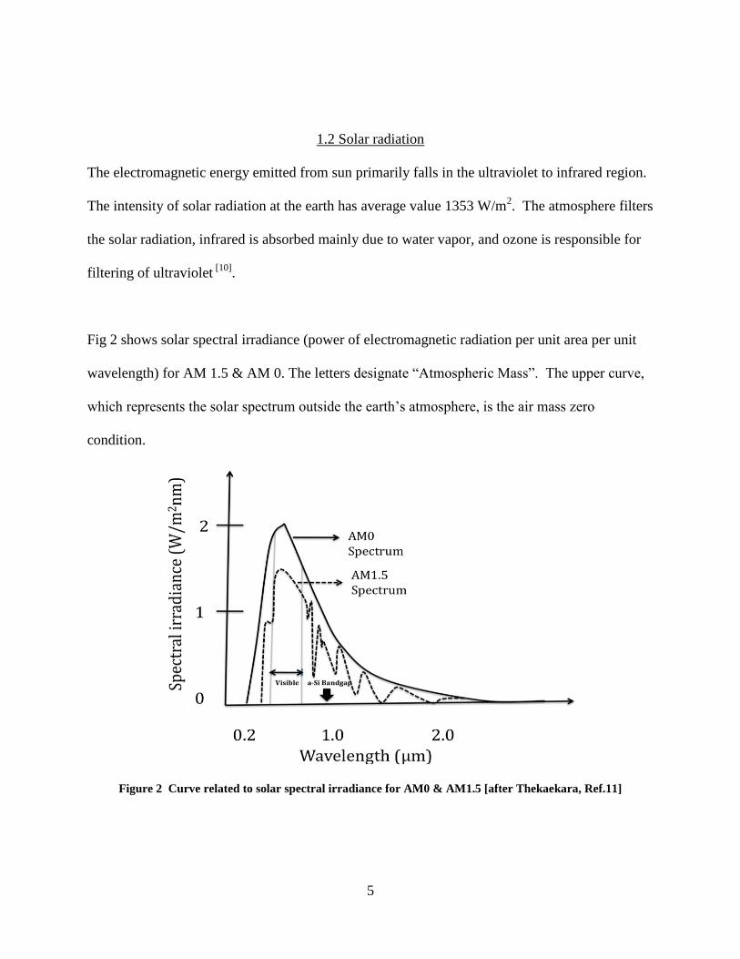
Fig 2 shows solar spectral irradiance (power of electromagnetic radiation per unit area per unit
wavelength) for AM 1.5 & AM 0. The letters designate “Atmospheric Mass”. The upper curve,
which represents the solar spectrum outside the earth‟s atmosphere, is the air mass zero
condition.
Figure 2 Curve related to solar spectral irradiance for AM0 & AM1.5 [after Thekaekara, Ref.11]

6
The AM0 spectrum is the relevant one for satellite and space vehicle applications because solar
radiation does not pass through the atmosphere in this case. AM 1 spectrum is considered when
sun is at zenith so radiation has to pass through one atmosphere distance. AM 1.5 is the energy-
weighted spectrum corresponding to the sun at 48.20 below the zenith.
Figure 3 Depiction of different air mass conditions
The most useful part for photovoltaic applications is the wavelength range 400-800 nm, which
corresponds to approximate photon energies of 1 - 2 eV. It is optimum to use material with band
gap of 1.5 eV for maximum absorption of solar spectrum. The band gap of single crystal silicon
is 1.14 eV.
1.3 Ideal conversion efficiency of solar cell
Performance parameters such as Fill Factor (FF) and Efficiency are obtained from I-V
characteristic of the device. The I-V characteristics of such a device are given by[12]
,
I = Is (eqV/kT
– 1) - IL (1)

7
The source IL results from the excitation of excess carriers by solar radiation; Is is the diode
saturation current, RS the series resistance, and RSH the shunt resistance. The series resistance RS
depends on junction depth, and the arrangement of ohmic contacts at the front surface.
Figure 4 (Left) Solar cell equivalent circuit. (Right) Energy diagram of p-n junction while irradiated by solar
flux.
Saturation current density is given by;
JS IS /A qNCNV1
NA
Dn
n
1
ND
Dp
p
e
Eg /KT
(2)
Where, A is the device area, NC the effective density of states in the conduction band, NV the
effective density of states in the valance band, ND the donor impurity concentration, and NA the
acceptor impurity concentration. The saturation current Is is very small compared IL. By
choosing an appropriate load, close to 80% of the product IscVoc, equal to the maximum power
point value Pm, can be extracted. Isc is short-circuit current, and Voc is the open-circuit voltage of
the cell. Fig. 5 below is the I-V characteristic curve of a solar cell. We can also define quantities
Im and Vm that correspond to the current and voltage, respectively, for the maximum power point
Pm.
From Eq.1 we obtain for the open-circuit voltage (I = 0):

8
Voc kT
qlnIL
IS1
kT
qlnIL
IS
(3)
Figure 5 Current-Voltage characteristics of solar cell under illumination [After Prince, Ref 13].
Hence for a given IL, the open-circuit voltage increases logarithmically with decreasing
saturation current Is. The out put power is given by;
P = VI = IsV (eqv/kT
– 1) - ILV
(4)
The condition for maximum power can be obtained when dP/dV = 0, or
Im IsVmeVm IL 1
1
Vm
(5)
Vm 1
lnIL /Is 1
1 Vm
Voc
1
ln(1 Vm )
(6)
Where = q/kT. The maximum output power is given by

9
Pm ImVm IL Voc 1
ln(1 Vm )
1
(7)
The ideal conversion efficiency is the ratio of the maximum power output to the incident power
Pin.
=
Pm
Pin Vm
2IS (q /kT)eqVm / kT /Pin
(8)
Another important parameter is Fill Factor (FF), which is ratio (given as the percentage) of actual
maximum obtainable power (Im Vm) to theoretical power (Isc Voc).
Fill Factor (FF) =
Im Vm
Isc Voc (9)
The Conversion efficiency can be written in terms of Fill Factor by
=
Im Vm
PinFF IL Voc
Pin (10)
Should be Isc, not IL. To maximize the efficiency one should maximize Fill Factor, Short Circuit
Current and Open Circuit Voltage in the numerator in Eq 10.
1.4 Thin film solar cell
Thin film solar cells require less material, they are consequently light weight, and depending on
the substrate they may be flexible. These factors cut material, processing, and module
10
construction costs. Thin film solar cells are characterized according to material being deposited
on the substrate. Some of the examples are; Amorphous Silicon (a-Si), Cadmium Telluride
(CdTe), Copper Indium Gallium Selanide (CIGS), Dye Sensitized Solar Cell (DSC), and Organic
Solar Cells. The deposition of active layer on substrate is performed with various methods such
as vapor growth, RF glow discharge, and plating. The active layer is poly crystalline or
disordered, deposited on passive and electrically active substrates. In amorphous silicon (a-Si)
lower conversion efficiency and long term instability are caused by the weakened bonds in
comparison to the regular crystal lattice.
Due to an active layer of possible thickness of 1-2 µm in thin film solar cell, the absorption co-
efficient becomes a very important parameter. Since it is a function of wavelength, different
wavelengths penetrate different distances into active layer before the entire solar flux is
absorbed.
The decay of the light intensity on passing through a thickness x of an absorbing medium is
given by the Beer-Lambert law
I(x) = I0 exp[-x], (11)
Where is the absorption coefficient per unit length given by
And λ the wavelength, and the extinction constant. Near the absorption edge we have [14]
(h Eg )
(12)
where hν is photon energy, Eg the semiconductor bandgap, and γ a constant whose value depends
whether material has direct or indirect bandgap.

11
In case of direct bandgap material, the carrier can be excited directly from the valence band to
the conduction band without changing the crystal momentum, but in indirect bandgap material it
cannot do so.
Figure 6 Optical transitions: (Left) indirect transition involving phonon. (Right) direct transition in which,
only photon excites electron from valance band to conduction band.
Crystalline silicon is an indirect bandgap material with bandgap of 1.14 eV, but hydrogenated a-
Si has absorption characteristics similar to crystal with direct bandgap material of 1.6 eV. The
absorption coefficients of crystal and amorphous silicon are compared in Figure 7. The steep
increase in absorption at the highest photon energy for crystal silicon is due to the onset of direct
transitions to a higher lying band.

12
Figure 7 Absorption coefficients for a-Si is in range 104 to 10
5 cm
-1 in visible range of solar flux [Ref, 15]
The characteristic absorption depth is the inverse of the absorption coefficient, defined by the
distance into the material for which intensity of light is dropped by factor 1/e. According to Fig.
7, high energy photons can be completely absorbed by less a-Si than for c-Si, while red light
requires much thicker a-Si cells than suffice for c-Si. In our experience, sunlight may be
observed transmitting through crystal silicon as thick as 10 microns, and this transmitted light is
red.
Figure 8 presents a schematic of a thin film solar cell that does not succeed in absorbing all the
incident flux. If the material is a-Si, which is common for commercial thin film cells, the
situation depicted in Figure 8 would be most severe in the red portion of the spectrum.

13
Figure 8 Thin film solar cell is not able to harvest entire solar flux due to low absorption coefficient value for
„visible red‟ & „infrared‟
According to Fig. 7, even 10 microns of a-Si absorbs only ~60% of the incident radiation at 800
nm wavelength. Usual a-Si thicknesses of ~1 micron in commercial cells absorb only 10% of
the light at this wavelength. Thus a significant portion of the solar spectrum is not harvested by
thin film silicon solar cells.

14
CHAPTER TWO: PLASMONIC NANO STRUCTURES IN PHOTO
VOLTAICS
2.1 Plasmonic nano structures as scattering centers
The semiconductor must absorb photons in order to produce electrical current. Crystal silicon, an
indirect gap semiconductor absorbs relatively weakly in the visible spectrum. Like many
semiconductors, it also has a high index of refraction (n = 3.42), such that 30% is reflected from
the front surface, according to R = (n-1)2/(n+1)
2. To avoid this, conventional thick solar cells use
inverted pyramid structures approximately 10 μm in diameter etched into the surface, which uses
total internal reflection to reduce the reflectance and improve absorbance of incident light. This
arrangement is not possible in case of thin film solar cells since they are only a few micrometers
thick[16]
. For such cells, scattering centers may serve some of the same function in reducing
reflection as do etched pits for thick cells.
There are number of ways to achieve light trapping in thin film solar cells by metallic
nanostructure that support surface plasmons. The light hitting the surface of solar cell with
metallic nano particles on top of it excites the localized surface plasmons on the nano particles,
which re-radiates the light into the active layer of cell in such a way that it is trapped inside the
cell[16]
. Fig. 9 shows this schematically.

15
Figure 9 Employing metal scattering centers increases the optical path length of thin film solar cell.
The strong interaction of light and nanoparticles leads to creation of strong dipole radiation at the
plasmon resonance frequency, resulting in an enhanced near field as shown in Fig 10. The
amount of light absorbed by the semiconductor is also increased resulting in to generation of
more electron-hole pairs. Dipole radiation generated from nano structures also increases the
photon density in near by semiconductor. Thus plasmonic nanostructure are also capable of
changing the optical properties near the semiconductor surface, which can increase the
absorption of light[17]
, in principle.

16
Figure 10. Field intensity enhancement around 100 nm diameter silver cylinder on quartz substrate
illuminated with plane waves from above [Ref 16]
This mechanism provides excellent opportunity of reducing the physical thickness of the
absorber while keeping sufficient optical thickness. A thinner absorber has less bulk
recombination and gives higher value of Voc across the junction for the same photo generated
charge. Scattering provides an enhanced optical path length for photons that enter the absorber
layer at oblique angles, and then may become trapped inside the semiconductor by total internal
reflection. This longer path length exponentially increases the amount of light absorbed,
resulting in higher production of electron hole pairs, and thus higher Isc. For these reasons, it is
possible to enhance the efficiency of thin film solar cell using plasmonic nano structures at front
surface. Moreover, metal nano particles as scattering centers can be applied to any thin material,
not just silicon [16]
.
2.2 Localized Surface Plasmons
Surface plasmon polaritons are collective oscillations of electrons at the interface between metal
and dielectric. Localized surface plasmons are non-propagating excitons of conduction electrons
in metallic nanostructures, and they occur for metallic nano particles of size much smaller than
the metal‟s skin depth. The free electrons of metal nano particles are periodically displaced with

17
respect to the lattice of ions by the external electric field of incident light. The displacement of
electrons leads to creation of positive charges at the opposite surface and these positive charge
and negative electrons attract each other. This restoring force results in an electron oscillator[18]
.
Figure 11 External electric field of incident light displaces the electron from its lattice ions which results in
oscillating electron density
Considering a homogeneous metal sphere placed in an electrostatic field E0, one can calculate
potential inside and outside the sphere [19]
.
in 3m
2mE0rcos
(13)
out E0rcos m 2m
E0d3 cos
r2 (14)
Where r is the radius of the sphere, d the diameter of the sphere, is the frequency dependent
dielectric constant of sphere, we used notation as simple complex dielectric constant, and m is
the dielectric function of the embedding medium. Φout describes the superposition of the

18
externally applied field and that of a dipole at the center of the sphere. Rewriting the Φout by
introducing term p for dipole moment.
0 3
0
Φ cos4
out
m
p rE r θ
πε ε r
(15)
3
0 04
2
m
m
m
ε εp πε ε d E
ε ε
(16)
Eq.16 shows that the external field induces a dipole moment inside the sphere. One can introduce
the polarizability α, which determines the response of the bound system when placed in external
electric field.
0 0mp ε ε αE
(17)
4d3 m 2m (18)
A plasma resonance occurs when Re[ = - 2 m, and here the scattering and field magnitudes
are both enhanced. If () is described by the Drude model, and m = 1 (air or vacuum) result
leads to the Drude resonance condition.
According to Drude model;
() 1 2
p
2 i (19)

19
where ωP is the plasma frequency of the metal, ωτ is collision frequency responsible for damping.
Here ωτ = 1/τ, where τ is the relaxation time, which in order of magnitude is 10-4
sec at 300 K
for gold.
The real part of eq. (19) gives the dielectric function of the sphere
Re[()] 1 2
p
21
2
2
(20)
For large frequency close to p damping is small and the ratio / >> 1, giving
Re[()] 1 2
p
2
(21)
Putting Re[ = - 2 in Eq (21), leads to expression the plasmon resonance frequency of metal
sphere in free space, namely
p
3 (22)
Since different metals have different plasma frequency, plasmon resonance frequency varies with
The resonance blue shifts as value of m is reduced, so it is possible to control the resonance
frequency by controlling the surrounding dielectric medium.
One can calculate total fields H(t) = He-iωt
and E(t) = Ee-iωt
, then calculate Poynting‟s vector to
find energy related to electromagnetic waves, and end up with cross sections of absorption and
scattering. These are
20
Csca k 4
6| |2
8
3k 4d6 m
2m
2
(23)
and
Cabs k Im 4kd3 m 2m (24)
In this case we assume that metal sphere is sub wavelength size, i.e. d<<λ. Both are enhanced at
resonance.
This scattering cross section is proportional to d6/
4, which shows strong size dependence for the
scattering. Eq. 23 suggests that as the particle size increases the scattering cross section should
continue to increase, but it is not the case for particles with size more than free space
wavelength, where the quasistatic approximation is not followed. For larger particle incident
plane wave of electric field can not be approximated as constant at any instant of time across the
entire particle, so one has to consider retardation effect leading to higher order multipoles as
shown in the figure 12. The particle with size 300 nm show broad range dipole resonance at 480
nm, quadrupole resonance at 380nm and octopole resonance at 350 nm. The particles with larger
diameter such as 0.4 m also show 16-pole resonance [31]
.

21
Figure 12 Extinction coefficient as function of wavelength, 120 nm diameter particles show dipole resonance
at 430 nm and quadrupole resonance at 355 nm [from Reference 31].
Mie‟s formulation of expansion of first TM mode explains this as follows,
mie 1 (1/10)( m )x 2 O(x 4 )
1
3
m m
1
30( 10m )x 2 i4 2m
3 / 2 V
30
O(x 4 )
V
(25)
Where x = sphere/0 is the size parameter with sphere is the diameter, and 0 wavelength of light
in vacuum. The second order term in the denominator describes the energy shifting to red due to
retardation effect. The third term is imaginary, and represents the radiative loss. The forth order
term in numerator and denominator describes the correction to the second order term[30]
.
Sub-wavelength size particle is crucial for confinement of optical energy as application for Solar
cells. Plasmon resonance frequency depends both on size and geometry of metallic particle.
Scattering cross sections of particle are enhanced near the resonance, which is prime motivation
for using Plasmonic centers to improve the efficiency of thin film solar cells. The resonance

22
frequency shifts to „red‟ as the particle size is increased. Intuitively we can understand
Figure 13 Dependence of Plasmon resonance frequency on particle size and geometry [Ref, 18]
that as the particle size increases, the depolarization field decreases resulting in to lower
resonance frequency. The quality factor Q and field strength f are important parameter to
understand Surface Plasmon Resonance. The quality factor Q of the surface Plasmon describes
the number of oscillation of SP before it decays out. Q also determines the increase in the
amplitude of the local electric field when surface Plasmon resonance takes place. Nobel metals
are chosen as prime candidate as scatters because of their high conductivity and being resistant to
corrosion while exposed to atmosphere and they have resonance frequency in visible range,
which is highly applicable to solar cells. Oscillator field strength f is a number of conduction
electrons in nano particle. Absorption cross section is proportional to f and Scattering cross
section is proportional to f2[18]
.
2.3 Lithographically produced ordered array of nano particles
Many groups have shown that lithographically produced or self-assembled arrays of metal nano
particles increase efficiency of thin film solar cells[2]
. The absorption and scattering of nano
particles is size and wavelength dependent, so it is important to optimize the particle size to
ensure the maximum scattering occurs in the spectrum of interest. In case of silver, absorption

23
dominates when the particle size is < 50 nm, leading to localized heating. This can be very
useful for thermal detectors but in case of solar cell application we need maximum amount of
scattering. Scattering occurs when particle size is more than 100 nm, however particle size
should not be too large, as it would lead to multipole oscillations, which would eventually reduce
the scattering[20]
.
Figure 14 shows the normalized extinction Cabs + Csca of 100 nm Ag nano particles, from ref. [2].
As one can see when air is the embedding medium, the resonance peak occurs at 390 nm. It
confirms that as the dielectric constant of embedding medium increases, the resonance shifts to
red. Au and Ag are perfect metals because of similar dielectric constants. Ag has issue of
oxidation, which reduces the scattering after a few days [27]
.
Figure 14 Extinction (solid lines) & Scattering (dashed lines) cross section for Ag nano particles of 100 nm
size on different embedding medium such as air(black), Si3N4(blue) and Si(red) [reference 2]. It can be
noticed that scattering cross section is enhanced in very limited region for all the embedding mediums.

24
Though it is possible to control the size and pitch of the nano particles specifically in
lithography, the disadvantage of following this route is that the photocurrent enhancement is
achieved in only a specific range of solar spectrum depending on size and geometry of the
deposited particle. Moreover, the production of metal nano particles through photolithography is
expensive.

25
CHAPTER THREE: EXPERIMENT
3.1 Deposition of gold black thin film on solar cell
This report explores the possibility of using “gold blacks”, a nano-structured material that has
been exploited for decades as a broadband surface absorber for bolometers. Gold blacks are
produced cheaply and quickly in a low-vacuum process using method of Harris requiring no
lithographic patterning [3-7]
. Gold blacks have broad size distribution depending on deposition
parameters such as inert gas pressure, deposition rate and the mass of the gold in the boat[21-25]
.
The density of gold black is much less than bulk gold. The packing fraction and particle size can
be easily controlled by inert gas pressure[26]
. Thus, they have the potential to enhance light-
harvesting efficiency over a broader range of the solar spectrum than lithographically patterned
metals. For thermal detectors, thick opaque films are required [27]
. For solar cell, a thin film is
needed to allow scattered light to reach the semiconductor.

26
Figure 15. Gold Black deposition uses a thermal evaporation chamber back filled up to ~1 Torr with N2.
Very thin, porous films gold black with low packing fraction were first deposited on a substrate
by thermal evaporation in a chamber that was back-filled to ~1 Torr with N2. At such pressures,
the evaporated metal particles are able to combine into nano-scale agglomerates before reaching
the substrate. For the first batch of standard single crystal solar cells, each evaporation used
either 0.5 or 1.5 mg of gold in a Molybdenum boat, and proceeded until all the gold in the boat
was exhausted.
We deposit gold-black on two separate substrates simultaneously. These are placed side by side
within the evaporation chamber. One is a silicon square of 1 cm2 dimension to be used for SEM
(Scanning Electron Microscope) and PEEM (Photo Emission Electro Microscopy)

27
characterization experiments. The other is a solar cell. Both substrates are mounted on copper
holders to dissipate radiant heat absorbed during the evaporation.
Steps to deposit gold black film are as follows. The chamber is evacuated to a pressure of 10-4
Torr with a diffusion pump. The substrate is cooled to ~30 0F. Current in the amount of 60-70 A
is passed through the Mo boat to evaporate the gold contained within. The current is turned off,
and the temperature of the substrate brought up to room temperature to avoid condensation when
the chamber is vented.
We performed the deposition of gold black on two different types of solar cells. The first type
was standard thick single crystal solar cell and the later was commercial amorphous thin film
solar cell (PowerFilm). Two level full factorial experiments were performed on thick crystal Si
cells first. No improvement was expected for thick cells since they absorb all the light anyway.
None was observed. The purpose of these experiments was to establish deposition,
characterization, and statistical analysis procedures.
Second, we investigated thin-film a-Si solar cells. Here an efficiency enhancement effect was
expected to be possible, and such was discovered. However, in the process of completing a two
level full factorial optimization protocol on these cells, additional sources of uncertainty were
discovered that hinder accurate quantification of the efficiency enhancement. The two-level full
factorial experiment was halted in the middle, and separate experiments performed to identify the

28
causes of uncertainty. Lessons learned suggested changes to the characterization approach that
will be implemented in future work.
We here present the experiments on the thick cells. The statistical approach to the experiment on
thick c-Si cells is presented in Table 1. The independent variables are the pressure of the buffer
gas, the current through the boat (which determines the evaporation rate), and the starting mass
of metal. Upper limit values of the independent variable are denoted by “+” and lower limit
values are denoted by “-“. A 2 level full factorial requires two sets of eight runs (23), one for
each combination of the three parameters. Additionally, four runs are performed at the mid
points of the parameter ranges for a confidence level of 95%. The middle points are denoted by
“*” in the table. The dependent variables, or responses, are the change in efficiency and the
percent surface coverage. The order of the film preparation was randomized to avoid systematic
effects. Interactions between the dependent variables have been analyzed and response surfaces
plotted in order to find the maxima. The parameters were chosen after several test runs and are
as follows: (+) current = 68 A, (-) current = 58 A, (*) = 63 A; (+) N2 pressure = 1000 mTorr, (-)
= 400 mTorr, (*) = 700 mTorr; (+) mass Au = 1.5 mg, (-) = 0.5 mg, and (*) = 1.0 mg.

29
Table 1 Two-level full factorial protocol and order of experiments
Run x1 x2 x3
1 - - +
2 - + +
3 + - +
4 + + +
5 - - -
6 + - -
7 + + -
8 - + -
9 * * *
10 * * *
11 + + -
12 + + +
13 + - -
14 - - -
15 - + +
16 - + -
17 + - +
18 - - +
19 * * *
20 * * *
From the data collected for samples according to parameter values in Table I, we may predict
responses at other parameter values according to Eq. 21
YPR = a0 + a1x1 + a2x2 + a3x3 + a12x1x2 + a13x1x3 + a23x2x3 + a123x1x2x3 , (21)
Where the coefficients an are determined from the factor effects and xn are the factor variables.
3.2 Characterization of Solar Cell
Characterization setup for the Solar Cell included a Xenon lamp, which produced 350 mW over
a 50 mm diameter spot at sample through AM 0 and AM 1.5 filters combined and optics, which
is about 13% the power of 1 sun. Uniformity of measurement was insured by plotting the
response of a photodetector at different locations within the illumination spot as shown in figure
16. The illumination is apparently fairly uniform within the central 1 square inch area.

30
-1
0
1
2
0.0
0.2
0.4
0.5 1.0 1.5 2.0 2.5 3.0
Y position (inches)
Voltage (
V)
X p
ositio
n (
inches)
Figure 16 Response of photo-detector at the different locations on the spot formed with Xe lamp.
We measured the conversion efficiency of standard Si solar cells with & without metal-black
deposited on the surface. Characterization of the photo response and I-V measurements used a
Keithley SourceMeter, as shown in the photo of our set-up Fig. 17. A monochromator and filter
set allowed us to select narrow bands from within the spectrum, as shown schematically in Fig.
18. The photo current (Isc) response was recorded for solar cells with different metal black
depositions across the wavelength range of 350 to 1100 nm. The data was collected and
displayed in Labview.

31
Figure 17 Photograph of solar cell characterization facility.
Figure 18 Schematic of the photocell characterization set up. Monochromated Xe arc lamp light of calibrated
intensity passes through a filter to remove harmonics and impinges on the solar cell, whose IV curve is
measured.
The electrical characterization of solar cells, shown schematically in Fig. 19, results in an IV curve. As an example
we present our data for Power Film in Fig. 20. This cell consists of a thin amorphous silicon absorber layer on a
50-micron polymer substrate.

32
Figure 19 Current is passed trhough Solar Cell and Voltage is measured load resistance different load
resistences.
Figure 20. IV curve, plotted with power vs. voltage (circles), for the PowerFilm solar cell. MPP (maximum
power point) occurs at the knee.
The intersection with the voltage axis at zero current gives the open circuit voltage (VOC). The
intersection with the current axis at zero applied voltage gives the short circuit current (ISC). The
optimum operating point is at the “knee” of the curve, where the power has its maximum value.

33
The Maximum Power Point (MPP), ISC, and VOC are indicated on the plot. The intersection of
the dashed line with the IV curve gives the load resistance. The solar cell efficiency is
determined by ImVm/(incident optical power). Photocurrent enhancement factor is defined in
terms of short circuit current by E = Isc(p)
/Isc(ref)
, where the numerator corresponds to the
measurement with particles on the surface.

34
CHAPTER FOUR: RESULTS
4.1 Measurements on Standard Thick Single Crystal Solar Cell
The standard thick crystal-silicon solar cells were chosen first for experiment since their
commercial availability and uniform performance even though it was expected that gold black
film would just shade the front surface and decrease efficiency. Figure 21 (top) shows the
spectral response of one of the standard single crystal silicon solar cell samples. Plotted is
current as a function of wavelength, both before and after deposition of gold black. Fig. 21
(bottom) presents the ratio of the two curves. As expected, efficiency of optically thick solar
cells is lowered at all wavelengths due to shadowing. However, this decrease is slightly less in
the near IR, close to the indirect band gap, where absorption by the silicon is less efficient, which
is evidence that gold black deposition on front surface is increasing the optical path length of
incident solar flux.

35
400 600 800 10000
1
2
3
4
13x
Cu
rre
nt
(A
)
Wavelength (nm)
400 600 800 10000.0
0.2
0.4
0.6
0.8
1.0
aft
er/
be
fore
ra
tio
Wavelength (nm)
Figure 21. (top) Spectral characterization of an optically-thick Si solar cell. The black curve is the spectral
response of the Si solar cell before deposition, and the red is the response after coating. (bottom) Ratio of
“after” to “before,” showing an increase in the near IR. The response decreases less at longer wavelengths
where the silicon absorption is less and scattering by the small particles gives an increase in light harvesting,
which compensates somewhat the decrease caused by shadowing.

36
Since these cells are optically thick, efficiency improvement by addition of scattering centers
was never expected. The reason is that the silicon is already thick enough to absorb the entire
solar spectrum that is not reflected from the surface.
This full factorial experiment on thick film solar cell allowed optimizing both the deposition and
characterization processes in terms of efficiency and percentage coverage, which eventually
allowed us go observe an increase in the efficiency of gold-black coated thin film solar cells.
Fig. 22 presents response surfaces for efficiency, taken at the middle points at constant current
(left) and constant pressure (right). The maximum appears at the lowest mass of gold and the
lowest evaporation boat current (or lowest evaporation rate). The net change in efficiency was
negative for all of these thick crystalline silicon samples, as anticipated. The response surface
led us to conclusion that, small metal particles simply shade optically thick cells, so that less
coverage is better.
Figure 22. Response surfaces for efficiency, plotted as a function of gold mass and pressure at constant boat
current (left) and as a function of gold mass and evaporation boat current at constant pressure (right).

37
Response surfaces for coverage are plotted in Figs. 23 and 24. The minimum at lowest current
and lowest mass in Fig. 23 shows that smaller masses (obviously) and lower current (evaporation
rate) will lead to lower percent coverage. This observation informed the successful thin film
experiment by optimizing the process to avoid excessive shadowing.
Figure 23 Response surfaces for percent coverage at constant pressure.
The response surfaces in Fig 24 show results that are not intuitively obvious. Minimum
coverage occurs at lowest pressure and highest mass for constant current. This suggests that the
achieved gold black layer is a more open network for these conditions, with the mass of gold
highly concentrated. On the other hand, Fig. 22 showed that it was the higher pressures, even at
the highest mass, that gave the least efficiency decrease. This suggests that the larger gold
particles, though they cover the surface less, are nevertheless more effective at shadowing the
surface. Since scattering goes as the square of the particle volume (Eq. 23), and absorption by
the particle as its volume (Eq. 24), it suggests that there is an optimum particle size, above which
scattering actually hurts more than it helps. A secondary minimum in coverage at low mass and
high pressure can be attributed to just having less gold arriving at the surface.

38
Figure 24 Response surfaces for percent coverage at constant current.
4.2 Measurements on Thin Film Amorphous Silicon Solar Cell
The thin film solar cell investigated was an amorphous silicon cell from Power Film. This is
sufficiently thin that it is flexible. The absorption coefficient of amorphous silicon decreases
sharply in infrared, but there is still significant photocurrent generated out to wavelengths of
1100 nm as shown in Fig. 25.

39
400 600 800 10000.0
0.5
1.0
1.5
2.0
2.5
3.0
3.5
4.0
4.5
5.0
PowerFilm
Curr
ent (
A)
Wavelength (nm)
Before deposition
After deposition
After wiping surface
Figure 25 Demonstration of photocurrent increase across the spectrum for thin film solar cell coated with
gold-black particles. Photocurrent was measured under zero applied voltage.
After deposition of gold-black on the surface, the photocurrent increased by ~20% at most
wavelengths, while the improvement was less (~10%) at the peak of the photo response at 580
nm, namely that the improvement in photo response caused by scattering centers on the surface
should be strongest at those wavelengths where the absorption by the film alone is weakest. The
improvement disappeared when the deposited metal particles were wiped off. Since we removed
the gold black coating from this sample, we were not able to perform I-V measurement on it.
Another sample showed 6.9% efficiency increase and 12% improvement in Isc photocurrent
response (Fig. 26).

40
0.0 0.5 1.0 1.5 2.0 2.5 3.0 3.5 4.00
2
4
6
8
10
IV
Power
MPP
Cu
rre
nt
(mA
)
Voltage (V)
PowerFilm - before
MPP = 9.15 mW
0.0 0.5 1.0 1.5 2.0 2.5 3.0 3.5 4.00
2
4
6
8
10
PowerFilm - after
MPP = 9.78 mW
IV
Power
MPP
Cu
rre
nt
(mA
)
Voltage (V)
Figure 26 IV and photo-power curves for PowerFilm amorphous silicon solar cell for solar spectrum
irradiance. Also indicated on the IV curve is the Maximum Power Point (MPP). The maximum power point
before deposition was 9.15 mW. After deposition, the maximum power point increased by 7%.
The experiment was repeated with different deposition parameters, again we noticed efficiency
enhancement as shown in Fig 27. These results confirm that deposition of gold black with „right
morphology‟ increase the efficiency of thin film solar cells. It remains to identify the deposition
conditions that optimize the increase and to correlate the increase with film characteristics in
order to obtain an understanding based on physics. The former goal remains for future work.
Some progress toward the latter goal is described next.

41
Figure 27. Gold black increases the efficiency by 5.1%
4.3 Optimization and Understanding
Electrodynamics simulations and physical characterization can inform future optimization to
obtain higher efficiency enhancements. For the experimental characterization, we have Scanning
Electron Microscopy (SEM) and Photo Electron Emission Microscopy (PEEM). The SEM
images may be analyzed to obtain percent coverage and particle size distributions. PEEM
images can give spectral and spatial distributions of plasma resonance hot spots, where optical
scattering is enhanced. Electrodynamic simulations can reveal scattering and field
enhancements, where film parameters can be quickly changed and optimized using a computer.
4.3.1 Percentage coverage & Wavelet Analysis
SEM images determined the relationship between the controlled parameters and the morphology
of the nanoparticles. Example images are presented in Figs. 28 and 29. The percent coverage

42
was found from histograms of such images, i.e. from the ratio of the number of bright pixels
(gold black) to the total number of pixels in the image (Figures 28 and 29, right). The dark peak
of the histogram corresponds to substrate, while the bright shoulder is due to the gold black. To
separate them for the area analysis, the dark peak was assumed to be symmetrical.
0 50 100 150 200 2500
1x10⁴
2x10⁴
3x10⁴
4x10⁴
Co
un
ts
Pixel color
13x
Figure 28. (left) SEM image of lightly coated substrate. Goldblack film run #18 (0.5 mg Au, 400 mTorr, 68A)
from Table 1. (right) Histogram generated from this image. The fraction of coverage by gold black was
determined from the tail of the histogram that extends beyond ~100 on the brightness scale.
0 50 100 150 200 2500.0
2.0x10³
4.0x10³
6.0x10³
8.0x10³
Co
un
ts
Pixel color
6x08
Figure 29. SEM image and histogram of heavily coated sample. Sample 6x (run #12 – 1.5 mg Au, 1000
mTorr, 68 A).

43
Wavelet analysis for the image in Fig. 28 is plotted in Fig. 30. The peak shows that the mean
particle size occurs at ~2.3 m. The distribution of particle sizes ranges from 300 nm to 20
microns.
1 100
1x10⁶
2x10⁶
3x10⁶
Am
plit
ud
e
Wavelength (m)
13x
Figure 30. Results of wavelet analysis for the image in Fig. 28.
This broad distribution of particle sizes appears to be responsible for the broad spectral range of
the resonant enhancement for the entire spectrum in case of thin film solar cell as result shown in
Fig 25. Once data of percentage coverage and wavelet analysis is collected for full factorial
deposition parameters, one can be in better position to conclude what average particle size is
sufficient to ensure maximum scattering and avoid absorption.
4.3.2 Photo Electron Emission Microscopy (PEEM)
This technique provided information about the spatial distribution of the plasmon resonances,
which can be correlated with SEM images and PV measurements. PEEM uses a near infrared
laser to excite Plasmon resonances, and it gives a visual indication of field enhancement by
detecting electrons emitted from the thin films that are within the field of view of the instrument.

44
PEEM uses a cooled CCD camera to record photoelectron emission from samples that are
irradiated using sources such as mercury arc lamps and lasers. Wavelength tuning in visible and
near infrared causes resonances to appear in different parts of the sample surface due to the
distribution of particle sizes and surrounding dielectric environments.
Fig 31 (right) present photoelectron emission from gold-black samples using 800 nm wavelength
excitation, which has photon energy (1.5 eV) far below the work function of gold (5.1 eV), and
also below gold‟s plasmon resonance frequency for bulk surfaces (~2.5 eV). The emission that
occurs is a non-linear multi-photon effect due to the field enhancement at the plasmon
resonances. The lower left quadrant has been modified by a focused ion-beam mill (FIB) to
make a marker for alignment. First, we notice that the modified surface has different
morphology in the SEM image and is less bright in the PEEM image, showing that it has less
plasmon activity. Second, the distribution of bright-white hotspots in the PEEM image is less
dense in the modified region than one might expect from the distribution of comparable
structures in the SEM image. These results suggest that there is a range of parameters that effect
plasmon activity, giving wide scope for optimization.

45
Figure 31. SEM image (left) of a gold black sample. PEEM image of the same sample under Hg lamp
illumination (right). The field of view is 150 microns.
Fig. 32 presents preliminary results of the wavelength dependence for the PEEM images. The
two wavelengths are not very different, and consequently, the hot-spot distribution for the two
images is nearly identical. Nevertheless, the image for the longer wavelength shows more
contrast, i.e. the hot spots are brighter relative to the background. We suggest that this is because
the wavelength is now closer to the surface plasmon resonance wavelength for gold (~500 nm).
Figure 32. Gold black sample illuminated by a laser at two different wavelengths. (left) = 370 nm and
(right) = 420 nm.
PEEM images of gold black films with 50 micron field-of-view are presented in Fig. 33. The
bright areas correspond to photoelectron emission for laser illumination at 370 nm (left) and 420

46
nm (right) wavelengths. Again we see higher plasmon activity in the longer wavelength image
when we are closer to the bulk surface plasmon resonance wavelength of gold.
Figure 33. Left: PEEM image of gold black film under = 370 nm laser illumination. Right: under = 420
nm laser illumination.
“Hot spots” at each of the wavelengths are relevant to photovoltaic power generation. It is in
principle possible to optimize the parameters of deposition providing highest density of “hot
spots” when irradiated with source in the range of 400-800 nm.
4.3.3 Simulation
Through simulation one can visualize any system of nano particles on a substrate, to see how
intensity of incident field is behaving at different cross sections of the system, such as inside the
substrate or close to the nano particle.We generated a system with nano-scale gold spheres
placed on the surface of an optically thin silicon layer. The software package Lumerical solved
Maxwell‟s equations over a variable meshed field, giving spatial and spectral profiles of intensity
enhancements. The 3 dimensional layout is presented in Figure 34. This model has 100 nm gold

47
spheres located 100 nm from the surface of a 200 nm thick silicon wafer. The 532 nm light
source is incident from underneath and confined to the region defined by the white borders.
Figure 34 The model system for Electrodynamic simulation using Lumerical. A layer of 100 nm gold spheres
is located 100 nm in front of the surface of a 200 nm thick silicon wafer. Radiation is incident from outside
the wafer (purple arrow). Blue arrows indicate the polarization and the grey boxes define volume in which
the radiation is confined.
Fig 35 presents results of the simulation according to a monitor placed on the surface of the
silicon. Bright colors show field enhancement. The presence of bright red color at the top and
bottom edge of the silicon slab are evidence of lateral scattering by the metal particles and
waveguiding by the slab to its ends, where the light sprays out. This light is much more intense
(by two orders of magnitude) than the incident intensity, as evidenced by the light that passes
around the edges of the silicon at left and right. The smaller bright red patches at the right and
left edges of the silicon slab show that the direction of the scattering depends strongly on the
polarization of the incident polarized beam.
48
Figure 35. A monitor at the surface of the silicon wafer, showing the spatial profile of the intensity of the
radiation. The highest intensity is shown in red.
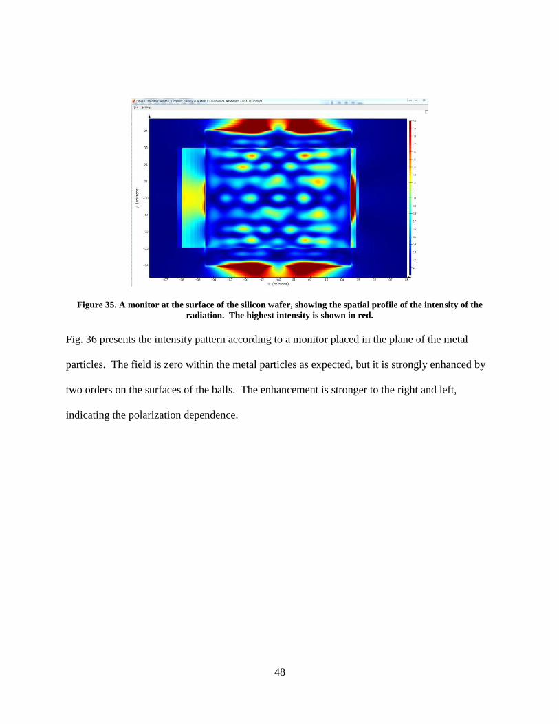
Fig. 36 presents the intensity pattern according to a monitor placed in the plane of the metal
particles. The field is zero within the metal particles as expected, but it is strongly enhanced by
two orders on the surfaces of the balls. The enhancement is stronger to the right and left,
indicating the polarization dependence.

49
Figure 36. A monitor in the plane through the center of the layer of gold particles. High intensity is seen
around the edges of the gold spheres and none is seen inside the metal, as expected.
Fig. 37 presents the intensity according to a monitor within the thin silicon slab, this section is
the most important of the three, since we need scattering inside the active layer. The intensity is
strongly enhanced within the slab by two orders of magnitude as a consequence of resonant
scattering by the metal particles. Moreover, the high intensity bleeding out the ends of the slab
at top and bottom shows that the scattered radiation is being channeled like a waveguide by the
silicon, giving a substantial increase in the effective optical path length.

50
Figure 37 A monitor 100 nm inside the silicon surface. The red regions show the very high intensity
enhancement due to the gold nanoparticles.
The enhancement depends on the wavelength of incident radiation and on particle size. Once we
find out parameters producing desirable gold black morphology we can visualize the intensity
enhancement and compare it with PEEM analysis of the same sample. Simulations can provide
the understanding of behavior of enhanced field, so it is possible to make experimental changes
in deposition parameters for even better results.

51
CHAPTER FIVE: CONCLUSION & SUMMERY
We initiated our experiment of depositing gold black as scattering centers for standard thick
crystal Si solar cells. Though none of the results in full factorial experiment shown efficiency
improvement for these single crystal solar cells, it helped us to optimize the deposition,
characterization, and analysis procedures, which eventually proved useful in our successful
demonstration of efficiency enhancement for a thin film solar cell.
The initial experiments on thin film solar cell showed 20% increase in short circuit photocurrent
response across major part of the spectrum, while 10% photocurrent enhancement was seen in
visible band where solar cell it self is able to absorb light more efficiently compare to infrared
region. Other samples also showed efficiency increase of 5.1%.
Particle morphology can be correlated with response function measurements and efficiency
enhancements to obtain a physics-based understanding of the optimization. Selected SEM
images were analyzed according to histograms and wavelet analysis to obtain percent coverage
and particle size distributions, respectively.
The role of plasma oscillations can be elucidated by correlating efficiency improvements with
PEEM images of resonance hot-spot distributions. These “hot spots” are regions of near field
enhancements and they can be correlated with PV measurements. It is desirable to have
maximum number of “hotspots” while we step up the light source in the range of 400-800 nm.
So PEEM provides possibilities for optimization of gold black film.

52
Simulations were performed on a system with silicon wafer substrate, gold particles and
polarized light. We saw field enhancement of many orders due to scattering and enhanced field
bleeding out from the side of the slab confirmed that field was being channeled inside the Silicon
substrate increasing the optical path length of incident field. Simulations show great potential for
further rapid optimization of thin film, once the dependence of film morphology on deposition
parameters is understood.
The project has potential to be expanded to aluminum and silver-black thin films. Silver has high
conductivity compared to aluminum. Both are more prone to oxidation than is gold.
Impregnation of the porous films with polymer vapors may improve adhesion, and durability
while protecting against oxidation. It also allows means to control the local dielectric
environment of the metal particles to shift the resonances. Mixtures of different metal blacks
with different plasma frequencies (e.g. Cu and Al) can be deposited with the goal of broadening
the spectral response of the enhancement.
Using light trapping through the resonant scattering by metal blacks, it is possible to construct
optically thick but physically thin photovoltaics, which would be able to harvest full solar
spectrum. Thus the use of plasmonic nanoparticles allows completely new solar cell design
which could be highly efficient and consuming much less material.

53
LIST OF REFERENCES
[1] Harry A. Atwater and Albert Polman, Nature Mater 9, 205 (2010).
[2] K.R. Catchpole and A.Polman, Appl. Phys. Lett. 93, 191113 (2008), Opt. Expr. 16, 21793
(2008).
[3] L. Harris, R. T. McGinnies, and B. M. Siegel, “The Preparation and Optical Properties of
Gold Blacks,” J. Opt. Soc. Am. 38, 582-589 (1948).
[4] L. Harris and J. K. Beasley, “The Infrared Properties of Gold Smoke Deposits,” J. Opt. Soc.
Am. 42, 134-140 (1952).
[5] L. Harris and A. L. Loeb, “Conductance and Relaxation Time of Electrons in Gold Blacks
from Transmission and Reflection Measurements in the Far Infrared,” J. Opt. Soc. Am. 43, 1114-
1118 (1953).
[6] L. Harris, “The Transmittance and Reflectance of Gold Black Deposits in the 15- to 100-
Micron Region,” J. Opt. Soc. Am. 51, 80-82 (1961).
[7] L. Harris and P. Fowler, “Absorptance of Gold in the Far Infrared,” J. Opt. Soc. Am. 51, 164-
167 (1961).
[8] Alfred Smee Voltaic Mechanism of man, London: Longman, Brown, Green, and Longmans.
p. 15. (1849).
[9] Jenny Nelson, Energy, Ch.21, extension 4. The physics of solar cells. Imperial Collage Press
(2003).
[10] C.E. Backus, Ed, Solar Cells, IEEE Press, New York, 1976.

54
[11] M.P. Thekaekara, “Data on Incident Solar energy,” Suppl. Proc. 20th
Annu. Meet. Inst.
Environ. Sci., 1974, p. 21.
[12] S.M. Sze, Ch.14, Physics of Semiconductor Devices, A Wiley – Interscience publication
(1981).
[13] M.B. Prince, “Silicon Solar Energy Converters,” J. Appl. Phys. Am 26, 534 (1955).
[14] R.A. Smith, Semiconductors, 2nd
ed., Cambridge University Press, London, (1979).
[15] R.A. Gibson, P.G. LeComber, and W.E. Spear, “Doped Amorphous Silicon and Its
Application in Photovoltaic Devices,” IEEE J. Solid State Electron Devices, ED-24 449 (1977).
[16] K.R. Catchpole, “Nanostructures in photovoltaics”, Phil. Trans. R. Soc. A 364, 3493-3503
(2006).
[17] J.S.Bieteen, D.Pacific, N.S.Lewis, & H.A. Atwater, “Enhanced radiative emission rate and
quantum efficiecy in coupled silicon nanocrystal-nanostructured gold emitters”, Nano Lett. 5,
1768 (2005).
[18] Mark I Stockman, Nano Plasmonics: The Physics behind the Applications, February,
Physics Today (2011).
[19] Stefan A. Maier, Ch.5, Plasmonics: Fundamentals and Applications, Springer
Science+Business Media LLC, (2007).
[20] S.Pillai & M.A. Green, “Plasmonics for photovoltaic applications”, Solar energy Materials
& Solar Cells 94 1481-1486 (2010).
[21] C. Doland, P. O‟Neill, and A. Ignatiev, “Particulate nature of solar absorbing films: Gold
black,” J. Vac. Sci. Tech. 14, 259-262 (1977).

55
[22] P. O‟Neill, C. Doland, and A. Ignatiev, “Structural composition and optical properties of
solar blacks: gold black,” Applied Optics 16, 2822-2826 (1977).
[23] N. Nelms and J. Dowson, “Goldblack coating for thermal infrared detectors,” Sensors and
Actuators A. 120, 403-407 (2005).
[24] A. H. Pfund, “The Optical Properties of Metallic and Crystalline Powders,” J.O.S.A. 23,
375-378 (1933).
[25] Justin W. Cleary, Robert E. Peale, Masahiro Ishigami, Christian W. Smith, Kevin Baillie,
Josh E. Colwell, Oliver Edwards and Chris Fredricksen, J. Materials Science and Engineering 5,
171-176 (2011).
[26] c. Donald, P. O‟Neill, and A. Ignatiev “Perticulate nature of solar absorbing films: Gold
Black” J.Vac Sci. Technol., Vol 14 No.1 (1977).
[27] Yu A Akimov and W S Koh, “Resonant and nonresonant Plasmonic nanoparticles
enhancement for thin-film silicon solar cells,” Nanotechnology 21, 235201 (2010).
[28] W. Becker, R. Fettig, and W. Ruppel, “Optical and electrical properties of black gold layers
in the far infrared,” Infrared Phys. & Tech. 40, 431-445 (1999).
[29] Justin W. Cleary, Robert E Peale, Masahiro Ishigami, Christian W. Smith, Kevin Baillie,
Josh E. Colwell, Oliver Edwards and Chris J Fredrickesen “ Effects of Polymer infusion and
Characteristic Length Scale on Gold –Black Long-Wave and Far-Infrared Absorbance” Journal
of Materials Science and Engineering 5, 171-176 (2011).
[30] Hitoshi Kuwata, Hiroharu Tamaru, Kunio Esumi, and Kenjiro Miyano, “ Resonant light
scattering from metal nano particles: Practical analysis beyond Rayleigh approximation” App.
Physics Letters., Vol 83 No.22 (2003).

56
[31] Dror Sarid & William Challener, “Modern Introduction to Surface plasmons, Theory,
Mathematica Modeling, and Applications” Cambridge University Press (2010).