mems - micro electrical mechanical systems · mems - micro electrical mechanical systems charles...
TRANSCRIPT

MEMS - Micro Electrical Mechanical Systems
Charles Jason BattlesPhysics TeacherMount Zion High School
Mentors: Dr. Papapolymerou, NickolasKingsley, and Ramanan Bairavasubramanian

MEMS
Micro Electro Mechanical Systems

Switches
In this case, RF (high frequency) switches with an average length of 200 microns, width of 50 microns, and height of 6 microns.

What are MEMS made of?
The switch itself is made of gold. The dielectric layer is made of silicon nitride.The substrate used is LCP (liquid crystal polymer). This was used because it is extremely cheap and very pliable.

MEMS Substrate RequirementsSmooth surface roughness
Roughness < MEMS heightFlat
For good lithographyChemical resistance
For fabricationTemperature compliance
For fabrication and operationUniform electrical properties
Uniform permittivity for high frequency devicesCHEAP!

What is LCP?
Chemically:2-Naphthalenecarboxylic Acid, 6-(Acetyloxy)-Polymer with 4-(Acetyloxy) Benzoic Acid1,4-benzenedicarboxylic acid (terephthalicacid), 4-hydroxybenzoic acid, and 4,4‘-dihyroxybiphenyl

What is LCP?A thermoplastic polymer made of aligned molecule chains with crystal-like spatial regularityWhen flowing in liquid crystal state, rigid segments of the molecules align next to one another in the direction of shear flowThis structure persists even after cooling below the melting pointRoughly 18 microns thick

What is LCP?
Commercially available from 25um-3mm thickAvailable bare, single, or double copper claddedCladding is 15-18um thickHas been researched since 1980s; used in high frequency applications since 1990s

The picture shows a switch in the up position.
Red Area: GoldGreen Area: Dielectric layer (usually silicon nitride) used to prevent metal-to-metal stiction, to decrease mechanical wear and tear, and to prevent DC contact.

How it works?
If you apply a DC voltage so that both ends of the switch are charged differently you create an electrostatic force. This force causes an attraction between the two areas.

Switch on.
The attractive force causes the switch to close. This allows theRF power to flow through the switch but the dielectric layer doesnot allow the electricity to flow through.
When the voltage is turned off the swich open back up. Without the dielectric layer the DC current would flow throughthe switch causing it to stick closed permenantly. It would be a one time switch.

Advantages
Advantages of using MEMS switches over solid state switches (i.e. PIN diodes, JFET):Can be designed for any frequency (Other only good up to a few GHz)Can be fabricated on wafer (Other require solding)Much less power lossExcellent RF isolation
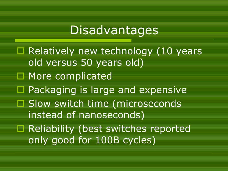
Disadvantages
Relatively new technology (10 years old versus 50 years old)More complicatedPackaging is large and expensiveSlow switch time (microseconds instead of nanoseconds)Reliability (best switches reported only good for 100B cycles)
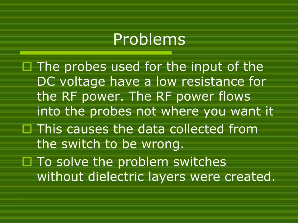
Problems
The probes used for the input of the DC voltage have a low resistance for the RF power. The RF power flows into the probes not where you want itThis causes the data collected from the switch to be wrong.To solve the problem switches without dielectric layers were created.

Why do this?Without the dielectric layer the switch will come on and not be able to open back up.Normally this would be bad but because the DC probes are creating a problem this would allow for them to be removed so that measurements could be taken accurately.Unfortunately this did not work as effectively as hoped.Next new switches were made and tested using normal scenarios.The dielectric layer becomes charged over time and begins to hold the switch down even when the DC power is off. Using the property allows for the results to be taken after the layer has become charged.

My contributions
I helped complete performance evaluations of MEMS switches.I helped to set up the equipment and run simulations. Unfortunately because of the clean room restrictions I was unable to help in fabrication. My current mentor, Nickolas is working on the MEMS switches in phase shifters.

Simulation
http://www.uk.comsol.com/showroom/animations/

Storage
All of the research material is storedin the container which is filled with Nitrogen.

Setting up the equipment.

Here is the switch that I tested.

What are MEMS switches for?
Coplanar Wave Guide Pads: Used to apply the input RF signal and to collect the output RF signal.Radial Stubs: Used to apply DC voltage for MEMS switch actuation. Also prevents RF power from leaking into the DC voltage source.MEMS Switches: When no DC voltage is applied to the Radial Stubs, the switches remain in the OFF state. When a DC voltage is applied, the switches actuate or turn ON.

How does a phase shifter work?Signal Path: The RF signal will either propagate through the top path or bottom path, depending on which set of MEMS switches are actuated (turned ON). Since the top path is longer than the bottom path, the signal takes longer to propagate through the top path than the bottom path. Therefore, a phase shift is implemented. Example: For a 1 GHz signal (period, T, 1ns), it takes 125ps forthe signal to propagate through the bottom path (shown in red) and 250ps for the signal to propagate through the top path (shown in blue). Therefore, we can calculate the phase difference as:So this would be a 45 degree phase shifter.

Where and how will it be used?The overall goal is to create a weather device that will be placed in space. The goal of this project is to develop dual-frequency (14/35 GHz), dual-polarization radar and radiometers to monitor precipitation patterns to improve our scientific understanding of the Earth’s environmental system and investigate its response to natural and man-made changes. The common requirement in such systems is the need for low-cost, low-mass, deployable antennas with large surface area that can be rolled-up or folded for launch and then deployed in space. To overcome the drawbacks of current solutions (parabolic reflectors, reflectarrays) for such applications, a liquid crystal polymer based microstrip antenna array is proposed and its feasibility for integration of different microwave components to realize scannablearrays is investigated.

MEMS Switch Zoomed Out

MEMS Switch Zoomed In

SEM Photo of single supported MEMS Switch

SEM Photo of double supported MEMS Switch
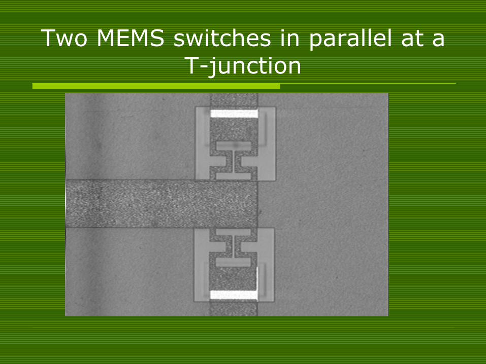
Two MEMS switches in parallel at a T-junction

Special Thanks
All images and diagrams were created or taken by Nickolas Kingsley.Thanks to Nicholas for all of his time and patience.Thanks to Dr. Papapolymerou for all of his help and ideas for lessons to integrate the advanced science into the classroom.

ReferencesXuefeng Wang, Jonathan Engel, and Chang Liu, “Liquid crystal polymer (LCP) for MEMS: processes and applications,” Journal of Micromechanics and Microengineering, pp. 628-633, May 2003.
Xuefeng Wang, Liang-Hsuan Lu, and Chang Liu, “Micromachining Techniques for Liquid Crystal Polymer,” University of Illinois at Urbana-Champaign.
Xuefeng Wang, Liang-Hsuan Lu, and Chang Liu, “Liquid Crystal Polymer (LCP) for MEMS Applications,” University of Illinois at Urbana-Champaign.
Xuefeng Wang, Jonathan Engel, and Chang Liu, “Liquid Crystal Polymer (LCP) for MEMS Applications,” University of Illinois at Urbana-Champaign.
Dane Thompson, Olivier Tantot, Hubert Jallageas, George Ponchak, Manos Tentzeris, John Papapolymerou, “Characterization of Liquid Crystal Polymer (LCP) Material and Transmission Lines on LCP Substrates From 30 to 110 GHz”, IEEE Transactions on Microwave Theory and Techniques”, Vol. 52, No. 4, April 2004.John Hiltz and John Power, “A Compendium of Thermoplastic Polymer Pyrograms,” Defense Research and Development Canada, July 2002.G. C. Xu, Y. Hibino, Y. Suzuki, M. Tanihara and Y. Imanishi, “Surface Modification of Polymers by Ion Implantation for Biocompatible Materials: Relations of Platelet Adhesion to Irradiation Effects,” IEEE, pp. 1144-1147, 1999.H. Biederman and D. Slavinska, “Ion Bombardment of Organic Materials and its potential Application,” IEEE, pp. 815-819, 1999.Edwin Culbertson, “A New Laminate Material for High Performance PCBs: Liquid Crystal Polymer Copper Clad Films,” IEEE, pp. 520-533, 1995. “Coplanar Waveguide Calculator,” http://www.rfdh.com/rfdb/cpw.htm
“Microstrip Impedance Calculator,” http://www.emclab.umr.edu/pcbtlc2/microstrip.html
MatWeb Material Property Data, Data sheet for Silicon, Gallium Arsenide, and Ticona Vectra A950 Liquid Crystal Polymer (LCP), September 2004.
Efunda Engineering Fundamentals, Data sheet for LCP, http://www.efunda.com
Robert Collin, “Foundations for Microwave Engineering,” IEEE Press, New York, 2001.
“Micromachines,” http://mems.sandia.gov/scripts/index.asp
“Ansys,” http://www.ansys.com/applications/mems/whatis.htm
Rogers Corporation, Material Safety Data Sheet (MSDS) for R/Flex 3000 Series LCP Films, March 2003.
Rogers Corporation, Fabrication Guidelines for R/Flex 3000 Series LCP Films, January 2004.
Rogers Corporation, Data Sheet for Rogers R/Flex 3000 Liquid Crystalline Polymer Circuit Material, July 2004.J.H. Das and J.E. Morris, “Metal Diffusion in Polymers,” IEEE Transactions on Components, Packaging, and Manufacturing Technology,” Part B, vol. 17, no. 4, November 1994.

ReferencesD. Balaraman, S. Bhattacharya, F. Ayazi and J. Papapolymerou, 揕ow Cost Low Actuation Voltage Copper RF MEMS Switches,? 2002 IEEE International Microwave Symposium, Vol. 2, pp. 1225-1228, June 2002Bairavasubramanian, Ramanan. Email interview. 7/21/2005.Kingsley, N. (2005).http://www.mirctech.gatech.edu/notes/MEMS.docKingsley, N. (2005).http://www.mirctech.gatech.edu/notes/Filter.docBairavasubramanian, Ramanan. (2005). http://www.mirctech.gatech.edu/notes/Antenna.pptKingsley, N. (2005).http://www.mirctech.gatech.edu/notes/MEMSfab.pptKingsley, N. (2005).http://www.mirctech.gatech.edu/notes/MEMSFabProcess.docKingsley, N. (2005).http://www.mirctech.gatech.edu/notes/MEMS1.jpgKingsley, N. (2005).http://www.mirctech.gatech.edu/notes/MEMS2.jpgKingsley, N. (2005).http://www.mirctech.gatech.edu/notes/MEMS3.jpgKingsley, N. (2005).http://www.mirctech.gatech.edu/notes/MEMS4.jpgKingsley, N. (2005).http://www.mirctech.gatech.edu/notes/MEMS5.jpgKingsley, N. (2005).http://www.mirctech.gatech.edu/notes/MEMS6.jpg