measurement of the role of secondary electrons in euv resist exposures
TRANSCRIPT
cnse.albany.edu [email protected]
Measurement of the role of secondary
electrons in EUV resist exposures
June 12, 2013
International Workshop on EUV Lithography
Greg Denbeauxa, Justin Torok,a Ryan Del Re,a Henry Herbol,a
Sanjana Das,a Irina Bocharova,a Angela Paolucci,a Leonidas E. Ocola,b
Carl Ventrice Jr.,a Eric Lifshin,a Robert L. Brainarda
a. College of Nanoscale Science and Engineering, University at Albany
b. Argonne National Laboratories
cnse.albany.edu [email protected]
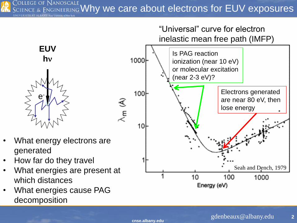
Why we care about electrons for EUV exposures
EUV
hn
e-
“Universal” curve for electron
inelastic mean free path (IMFP)
Electrons generated
are near 80 eV, then
lose energy
• What energy electrons are
generated
• How far do they travel
• What energies are present at
which distances
• What energies cause PAG
decomposition
Seah and Dench, 1979
Is PAG reaction
ionization (near 10 eV)
or molecular excitation
(near 2-3 eV)?
2
cnse.albany.edu [email protected]
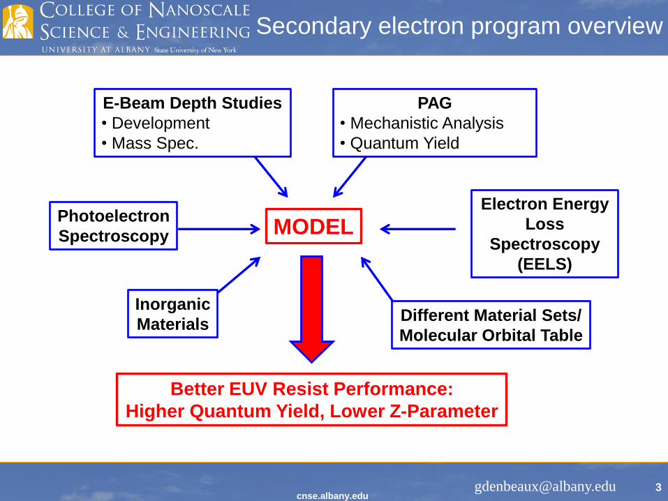
MODEL
Inorganic
Materials
Photoelectron
Spectroscopy
E-Beam Depth Studies
• Development
• Mass Spec.
Electron Energy
Loss
Spectroscopy
(EELS)
PAG
• Mechanistic Analysis
• Quantum Yield
Different Material Sets/
Molecular Orbital Table
Better EUV Resist Performance:
Higher Quantum Yield, Lower Z-Parameter
Secondary electron program overview
3

cnse.albany.edu [email protected]
How far do they go? Important for understanding
Resolution and LER
• From the central absorption event,
there will be a maximum range
(laterally) for the electrons.
• We measure the range by top down
exposures and measuring the depth to
represent the lateral electron travel
away from the EUV absorption site in
real exposures.
Bake and
Develop
Vary Dose
& Voltage
e- e- e-
Resist
Thickness Loss
(Ellipsometry)
Resist
EUV
hn
E-Beam Penetration Study:
• Expose commercial CAMP resist with 5-2000 eV
Electrons
• Bake, develop and measure penetration using
Spectroscopic Ellipsometry
4
e-
E-beam depth of penetration studies
cnse.albany.edu [email protected]
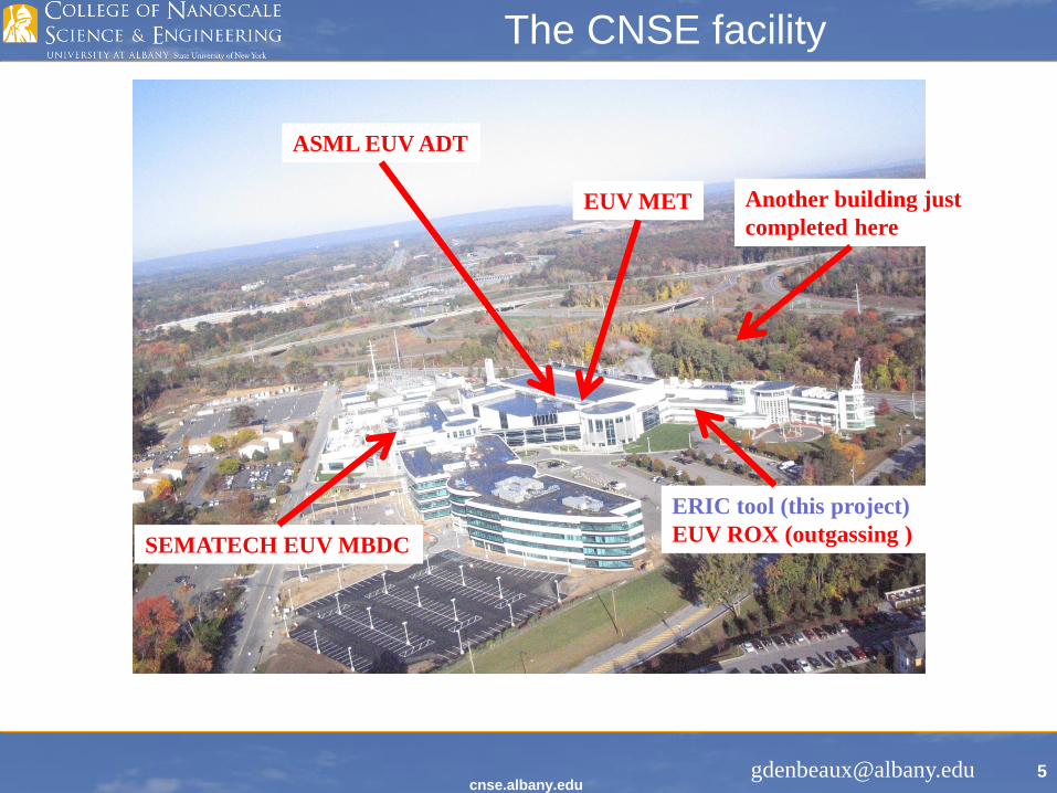
ASML EUV ADT
EUV MET
ERIC tool (this project)
EUV ROX (outgassing ) SEMATECH EUV MBDC
Another building just
completed here
The CNSE facility
5

cnse.albany.edu [email protected]
• Expose resist from 5-2000 eV across a range of doses.
• Bake and Develop
• Measure the thickness lost with ellipsometry (Woollam M-2000)
Mass spectrometer
E gun
Sample
Manipulator
Electron Resist Interaction Chamber (ERIC)
6

cnse.albany.edu [email protected]
0
20
40
60
80
100
120
Thic
kne
ss (
nm
)
Expose
(vary energy and dose)
Bake and develop
Ellipsometry for thickness
measurement
Process flow for depth measurements
Thickness lost is where sufficient reactions occur – not final stopping point of electrons
7

cnse.albany.edu [email protected]
0
10
20
30
40
50
60
0 10 20 30 40 50 60 70 80 90 100
Thic
kne
ss lo
st (
nm
)
Dose (uC/cm2)
0
10
20
30
40
50
60
0.1 1 10 100 1000
Thic
kne
ss lo
st (
nm
)
Dose (uC/cm2)
1000 eV 500 eV
100 eV
50 eV
1000 eV
500 eV
100 eV
50 eV
Electron penetration results – commercial resist
8
Higher energies penetrate deeper in resist – as expected
Thickness loss doesn’t saturate – indicating statistical distribution of electron penetration

cnse.albany.edu [email protected]
0
0.2
0.4
0.6
0.8
1
1.2
1.4
1.6
1.8
2
0 1 2 3 4 5 6 7 8 9 10
Nu
mb
er
of
rele
van
t re
acti
on
s (A
U)
depth in resist (nm)
0
0.2
0.4
0.6
0.8
1
1.2
1.4
1.6
1.8
2
0 1 2 3 4 5 6 7 8 9 10
Nu
mb
er
of
rele
van
t re
acti
on
s (A
U)
depth in resist (nm)
Illustration of process to measure relevant reactions at each depth from thickness loss
Assume there is a threshold number of reactions for clearing
Assume higher doses doesn’t physically change structure
Determine relevant reactions from penetration measurement
9

cnse.albany.edu [email protected]
0
0.1
0.2
0.3
0.4
0.5
0.6
0.7
0.8
0.9
1
0 5 10 15 20 25 30
nu
mb
er
of
rele
van
t re
acti
on
s (A
U)
depth (nm)
500 eV
100 eV
50 eV
0
10
20
30
40
50
0.01 0.1 1 10 100 1000
Thic
kne
ss lo
st in
nm
Dose in uC/cm2
Result indicates that electron energy for reactions
with PAG occur near 5-10 eV – or the electrons
would cause reactions deeper in the resist
For 50-100 eV electrons,
typical depth for reactions
is 2-3 nm
Determine relevant reaction depth
Results from measurement of commercial resist
10
cnse.albany.edu [email protected]
0
10
20
30
40
50
60
70
80
90
100
0.1 1 10 100 1000
Thic
kne
ss lo
st (
nm
)
Dose uC/cm2
1000 eV
500 eV
100 eV
50 eV
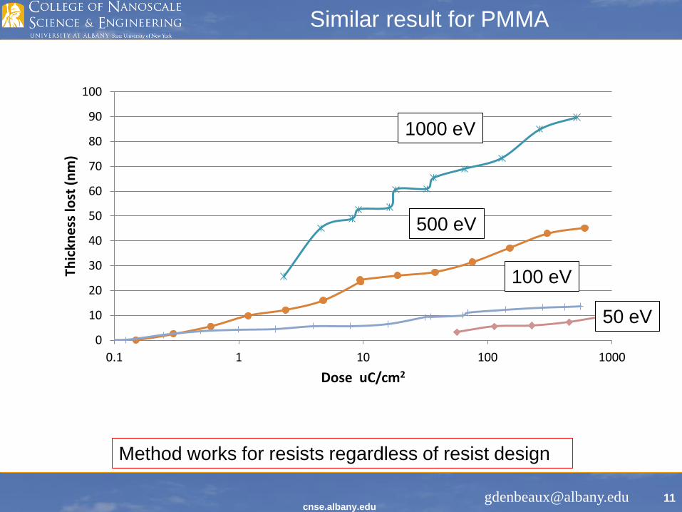
Similar result for PMMA
Method works for resists regardless of resist design
11
cnse.albany.edu [email protected]
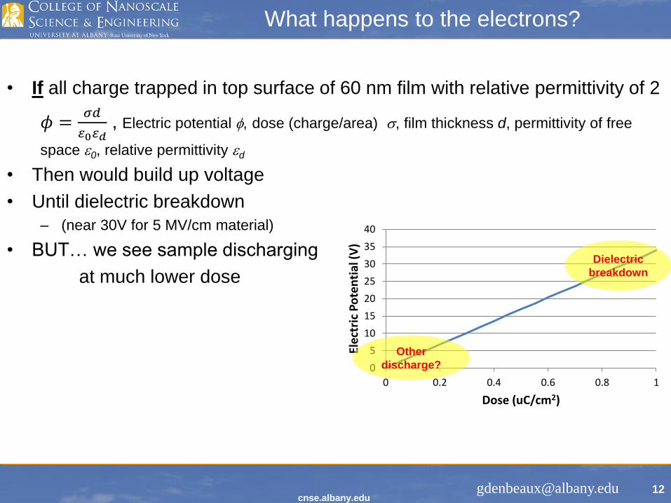
• If all charge trapped in top surface of 60 nm film with relative permittivity of 2
𝜙 =𝜎𝑑
𝜀0𝜀𝑑 , Electric potential f, dose (charge/area) s, film thickness d, permittivity of free
space e0, relative permittivity ed
• Then would build up voltage
• Until dielectric breakdown
– (near 30V for 5 MV/cm material)
• BUT… we see sample discharging
at much lower dose
0
5
10
15
20
25
30
35
40
0 0.2 0.4 0.6 0.8 1
Ele
ctri
c P
ote
nti
al (
V)
Dose (uC/cm2)
Dielectric
breakdown
Other
discharge?
What happens to the electrons?
12

cnse.albany.edu [email protected]
For 10 and 20 keV electrons:
– Charge builds up at lowest doses then is
stable – radiation induced conductivity
– Takes hours to discharge after exposure
– Is more negative for thicker films (more
trapped electrons)
J. Vac. Sci. Technol. B 17.6., Nov/Dec 1999
Past work with higher energy electrons
13
cnse.albany.edu [email protected]
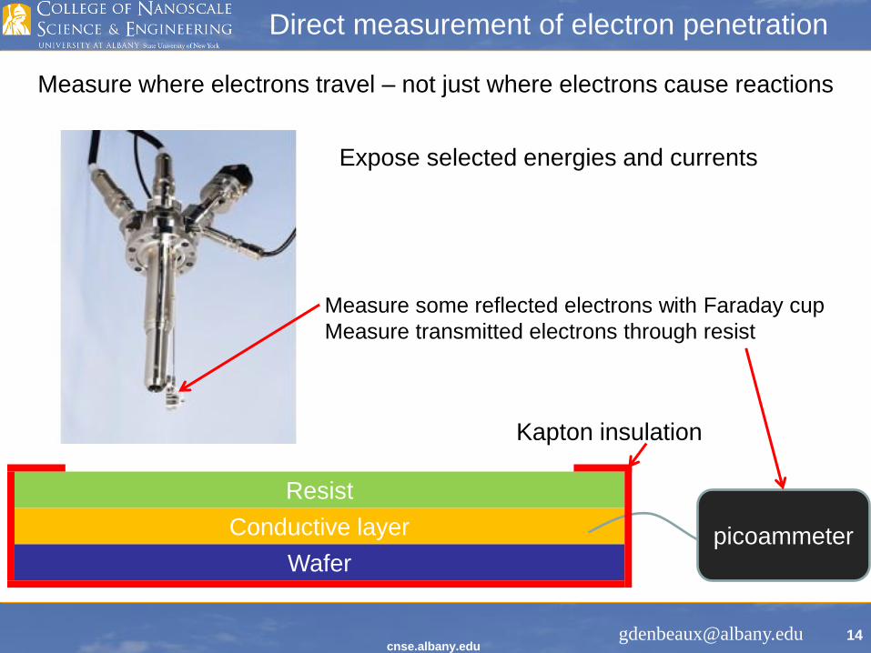
Measure where electrons travel – not just where electrons cause reactions
Direct measurement of electron penetration
Wafer
Conductive layer
Resist
picoammeter
Kapton insulation
Measure some reflected electrons with Faraday cup
Measure transmitted electrons through resist
Expose selected energies and currents
14
cnse.albany.edu [email protected]
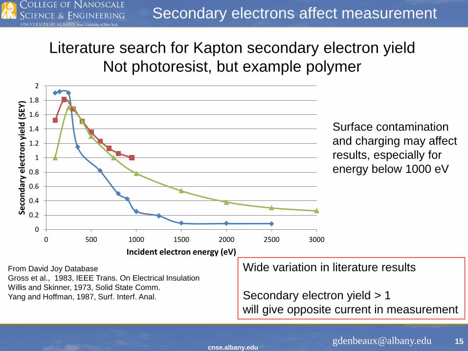
Literature search for Kapton secondary electron yield
Not photoresist, but example polymer
Secondary electrons affect measurement
0
0.2
0.4
0.6
0.8
1
1.2
1.4
1.6
1.8
2
0 500 1000 1500 2000 2500 3000
Seco
nd
ary
ele
ctro
n y
ield
(SE
Y)
Incident electron energy (eV)
From David Joy Database
Gross et al., 1983, IEEE Trans. On Electrical Insulation
Willis and Skinner, 1973, Solid State Comm.
Yang and Hoffman, 1987, Surf. Interf. Anal.
Wide variation in literature results
Secondary electron yield > 1
will give opposite current in measurement
Surface contamination
and charging may affect
results, especially for
energy below 1000 eV
15

cnse.albany.edu [email protected] 16
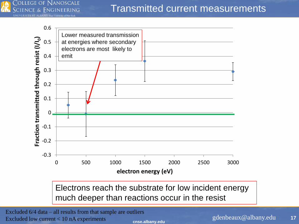
Transmitted current measurements
-80
-60
-40
-20
0
0 10 20 30 40 50
Cu
rre
nt
(nA
)
Time (s)
1500eV, 200nA incident
• Typical result that we want to see
• Current transmitted through
sample when electron gun is on
• Rise and fall time are picoammeter
response time
Lower energy is not as repeatable– charging effects?
-5
-4
-3
-2
-1
0
1
0 10 20 30 40 50
Raw
Cu
rre
nt
(nA
)
Time (s)
200eV, 200nA incident
-10
0
10
20
30
0 10 20 30 40 50Raw
Cu
rre
nt
(nA
)
Time (s)
200eV, 200nA incident
cnse.albany.edu [email protected] 17
Transmitted current measurements
-0.3
-0.2
-0.1
0
0.1
0.2
0.3
0.4
0.5
0.6
0 500 1000 1500 2000 2500 3000
Frac
tio
n t
ran
smit
ted
th
rou
gh r
esi
st (
I/I 0
)
electron energy (eV)
Electrons reach the substrate for low incident energy
much deeper than reactions occur in the resist
Lower measured transmission
at energies where secondary
electrons are most likely to
emit
Excluded 6/4 data – all results from that sample are outliers
Excluded low current < 10 nA experiments
cnse.albany.edu [email protected] 18
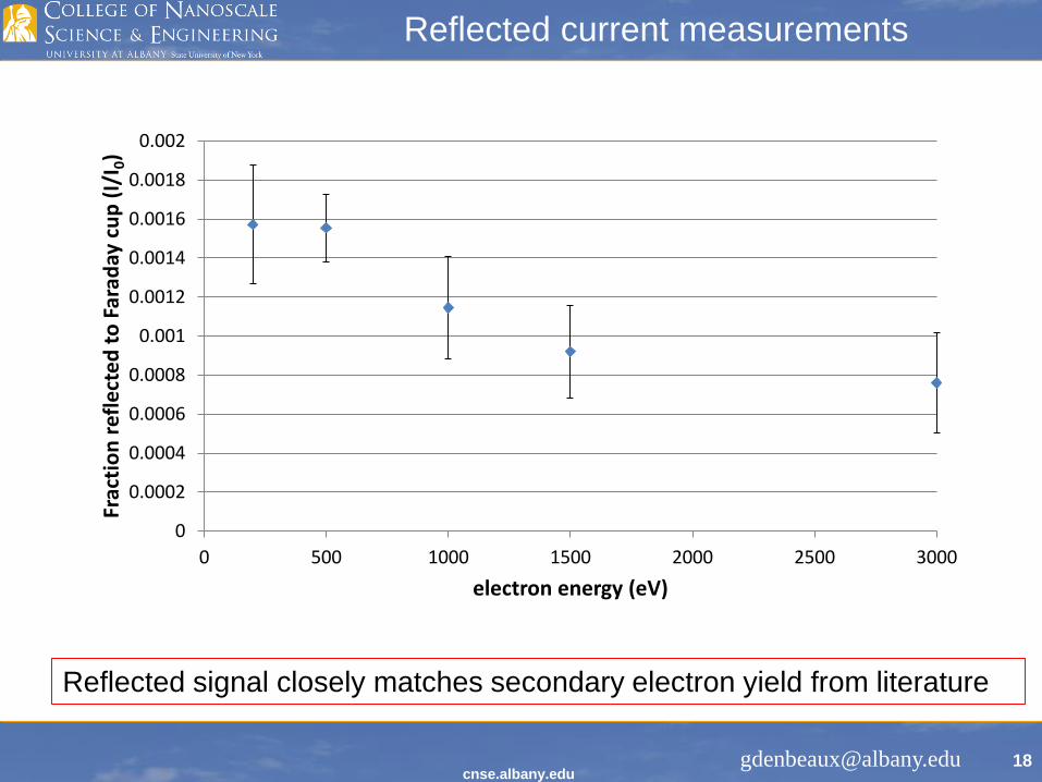
Reflected current measurements
0
0.0002
0.0004
0.0006
0.0008
0.001
0.0012
0.0014
0.0016
0.0018
0.002
0 500 1000 1500 2000 2500 3000
Frac
tio
n r
efle
cte
d t
o F
arad
ay c
up
(I/
I 0)
electron energy (eV)
Reflected signal closely matches secondary electron yield from literature
cnse.albany.edu [email protected]
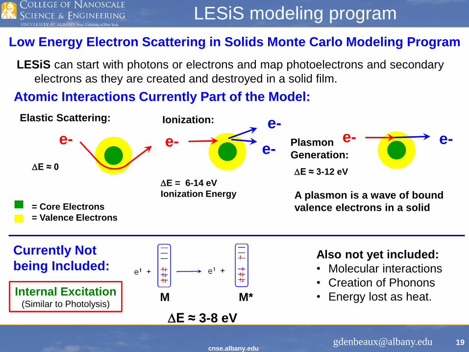
Low Energy Electron Scattering in Solids Monte Carlo Modeling Program
LESiS can start with photons or electrons and map photoelectrons and secondary
electrons as they are created and destroyed in a solid film.
Atomic Interactions Currently Part of the Model:
Elastic Scattering:
e-
= Core Electrons
= Valence Electrons
DE ≈ 0
e- e-
e- Ionization:
DE = 6-14 eV
Ionization Energy
e- e- Plasmon
Generation:
DE ≈ 3-12 eV
A plasmon is a wave of bound
valence electrons in a solid
Currently Not
being Included:
DE ≈ 3-8 eV
M M* Internal Excitation
(Similar to Photolysis)
Also not yet included:
• Molecular interactions
• Creation of Phonons
• Energy lost as heat.
LESiS modeling program
19
cnse.albany.edu [email protected]
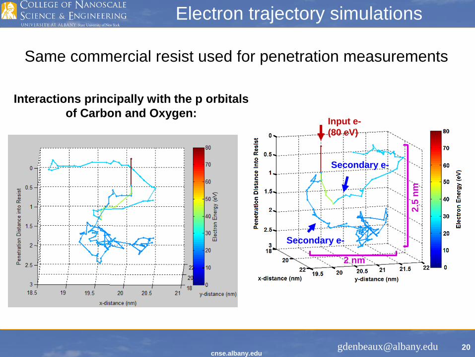
Same commercial resist used for penetration measurements
Secondary e-
Secondary e-
Input e-
(80 eV)
2 nm
2.5
nm
Interactions principally with the p orbitals
of Carbon and Oxygen:
Electron trajectory simulations
20
cnse.albany.edu [email protected]
Conclusions
• EUV resist exposures are based on electron chemistry
• We have developed a flexible experimental system to
help understand these electron reactions
• We have measured the electron blur directly
• We are using the data to help optimize the simulation
software
• We plan to • Determine the actual number and energy of electrons present in the
resist due to EUV exposure
• Determine the PAG reactivity – the cross section versus electron
energy
– In order to help in the development of improved efficiency resists
21
cnse.albany.edu [email protected]
Acknowledgments Thanks for helpful discussions
Ognian Dimov (Fujifilm)
Kevin Cummings (SEMATECH)
Thanks to CNSE for funding this work
22