matrix converter controlled with the direct transfer ... · international journal of electronics...
TRANSCRIPT

International Journal of Electronics
Vol. 92, No. 2, February 2005, 63–85
Matrix converter controlled with the direct transfer function
approach: analysis, modelling and simulation
J. RODRIGUEZy, E. SILVA*y, F. BLAABJERGz, P. WHEELERx,J. CLAREx and J. PONTTy
yDepartment of Electronic Engineering, Universidad Tecnica Federico Santa Marıa,Avda Blaceres 401, Valparaıso, Chile
zInstitute of Energy Technology, Aalborg University, Pontoppidanstraede 101,DK-9220, Aalborg East, Denmark
xSchool of Electrical and Electronic Engineering, University of Nottingham, University Park,Nottingham, NG7 2RD, England
(Received 17 April 2004; in final form 9 December 2004)
Power electronics is an emerging technology. New power circuits are inventedand have to be introduced into the power electronics curriculum. One of theinteresting new circuits is the matrix converter (MC), and this paper analysesits working principles. A simple model is proposed to represent the powercircuit, including the input filter. The power semiconductors are modelledas ideal bidirectional switches and the MC is controlled using a direct transferfunction approach. The modulation strategy of the converter is explained in acomplete and clear form. The commutation problem of two switches and thegeneration of overvoltages are clarified. The paper also includes a soft-switchingcommutation method that allows for a safe commutation of the switches.Finally a complete simulation scheme, using Matlab�–Simulink�, is discussed.
Keywords: Matrix converter; Modelling; Simulation; Teaching power conversion;Circuit analysis
1. Introduction
The transformation and control of energy is one of the most important processesin electrical engineering. In recent years, this work has been done with the use ofpower semiconductors and energy storage elements such as capacitors and induc-tances. Several converter families have been developed: rectifiers, inverters, choppers,cycloconverters, etc. Each of these families has its own advantages and limitations.The main advantage of all static converters over other energy processors is the highefficiency that can be achieved. One of the most interesting families of converters isthat of the so-called matrix converters (MCs).
The matrix converter is an array of bidirectional switches functioning as the mainpower elements. It interconnects directly the three-phase power supply to a three-phase load, without using any DC link or large energy storage elements, and there-fore it is called the all-silicon solution.
The most important characteristics of the matrix converter are: (1) simple andcompact power circuit; (2) generation of load voltage with arbitrary amplitude and
*Corresponding author. Email: [email protected]
International Journal of Electronics
ISSN 0020–7217 print/ISSN 1362–3060 online # 2005 Taylor & Francis Ltd
http://www.tandf.co.uk/journals
DOI: 10.1080/00207210512331337686

frequency; (3) sinusoidal input and output currents; (4) operation with unity powerfactor; and (5) regeneration capability. These highly attractive characteristics are thereason for the present tremendous interest in this topology.
The development of this converter starts with the early work of Venturiniand Alesina (Venturini 1980, Venturini and Alesina 1980). They presented thepower circuit of the converter as a matrix of bidirectional power switches andthey introduced the name ‘matrix converter’. Another major contribution of theseauthors is the development of a rigorous mathematical analysis to describe the low-frequency behaviour of the converter. In their modulation method, also knownas the direct transfer function approach, the output voltages are obtained bythe multiplication of the modulation matrix with the input voltages. A conceptuallydifferent control technique using the ‘fictitious DC link’ idea, was introducedlater (Rodrıguez 1983, Huber et al. 1989).
The simultaneous commutation of the controlled bidirectional switches usedin matrix converters is very difficult to achieve without generating overcurrent orovervoltage spikes that can destroy the power semiconductors. This fact affectednegatively the interest in matrix converters for several years until advanced multi-step commutation strategies appeared, that allowed safe operation of the switches(Empringham et al. 1998, Youm and Kuon 1999).
Another important limitation of matrix converters was the large number of powersemiconductors required to implement the bidirectional switches. This problem hasnow been overcome with the introduction of power modules in the market with thecomplete power circuit of the converter in a single chip.
The solutions of these important drawbacks are the reason for a new interest inthis topology. In effect, an important journal dedicated in year 2002 a special sectionto this technology as a recognition of the increasing interest in this area (Rodrıguez2002, Wheeler et al. 2002b).
Today, research activity is mainly dedicated to studying advanced technologicaland applications issues such as reliable implementation of commutation strategies(Mahlein et al. 2002b, Wheeler et al. 2002a), overvoltage protection (Nielsen et al.1997, Mahlein et al. 2002a), packaging (Klumpner et al. 2002b), operation underabnormal conditions (Blaabjerg et al. 2002, Klumpner and Blaabjerg 2002,Wiechmann et al. 2002) and filter design (Bernet et al. 2002, Klumpner et al. 2002a).
Several educators in the area of power electronics believe that matrix convertersare a very attractive topic for teaching, from a conceptual point of view, at graduatelevel. In addition, MC is becoming a mature technology and, for this reason, shouldbe included in Electrical Engineering courses. However, excellent and modern booksdo not cover this matter with enough depth (Mohan et al. 1995, Trzynadlowski1998), demanding a higher effort from the student to learn the concepts. Thereis therefore a need to develop new tools for teaching the theory of this powerconverter. In addition, the operation of the MC entails several practical problemssuch as complicated commutation of the switches and possible generation of over-voltages and overcurrents (Venturini 1980, Mohan et al. 1995, Wheeler et al. 2002b).These issues make the study of the MC using an experimental approach verydifficult. For this reason, a simulation approach appears to be a very good solutionfor the beginner student.
These authors have not found any publication concerning the simulation of MCs.Nor do popular circuit-oriented simulation software packages such as PSPICE andPSIM have the simulation of an MC as a standard block in their libraries. It is
64 J. Rodrıguez et al.
possible to simulate the operation of an MC using these circuit analysers, but thesimulation is usually limited to simple control andmodulation strategies. On the otherhand, it is possible to use a general equation solver such as Matlab�–Simulink�
to study the behaviour of this converter. This approach is more limited in the simula-tion of the semiconductors, but it permits the consideration of more complicatedcontrol strategies.
The primary objective of this work is to serve as a first approach to matrixconverters, covering both analysis and simulation of them using the direct transferfunction approach.
The paper is organized as follows: Section 2 presents the basic topology and theworking principle of the MC; Section 3 presents the modulation method of theconverter, based on the direct transfer function approach; Section 4 presents someapplication issues such as commutation problems, soft commutation strategy andovervoltage protection; Section 5 presents a detailed simulation scheme usingMatlab�–Simulink�; and Section 6 discusses some results. Finally, Section 7provides some concluding remarks.
2. Power circuit and working principle of the converter
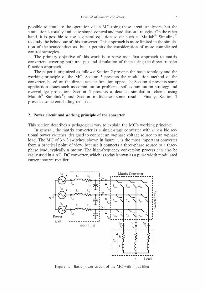
This section describes a pedagogical way to explain the MC’s working principle.In general, the matrix converter is a single-stage converter with m� n bidirec-
tional power switches, designed to connect an m-phase voltage source to an n-phaseload. The MC of 3� 3 switches, shown in figure 1, is the most important converterfrom a practical point of view, because it connects a three-phase source to a three-phase load, typically a motor. The high-frequency conversion process can also beeasily used in a AC–DC converter, which is today known as a pulse width modulatedcurrent source rectifier.
vsA
vsB
vsC
Lf
isA
isB
isC
Rf
Cf
iA
iB
iC
SAa
SAb SAc
SBa
SBb SBc
SCa SCb SCc
ia
ib
ic
R
L
n Load
switc
h ar
ray
input filter
Powergrid
N
vA
vB
vC
vaN
vbN vcN
Matrix Converter
Lf
Rf
Lf Rf
van
Figure 1. Basic power circuit of the MC with input filter.
Control of matrix converter 65

In the basic topology of the MC shown in figure 1, vsi, i ¼ fA,B,Cg, are thesource voltages, isi, i ¼ fA,B,Cg, are the source currents, vjn, j ¼ fa, b, cg, are theload voltages with respect to the neutral point of the load n, and ij, j ¼ fa, b, cg,are the load currents. Additionally, other auxiliary variables have been defined tobe used as a basis of the modulation and control strategies: vi, i ¼ fA,B,Cg, are theMC input voltages, ii, i ¼ fA,B,Cg, are the MC input currents, and vjN , j ¼ fa, b, cg,are the load voltages with respect to the neutral point N of the grid.
The filter (Cf ,Lf ,Rf ) located at the input of the converter has two mainpurposes:
(1) It filters the high-frequency components of the matrix converter inputcurrents (iA, iB, iC), generating almost sinusoidal source currents (isA, isB, isC).
(2) It avoids the generation of overvoltage produced by the fast commutation ofcurrents iA, iB, iC, due to the presence of the short-circuit reactance of any realpower supply.
It should be noted that Rf is the internal resistance of inductor Lf, not an additionalresistor.
Each switch sij , i ¼ fA,B,Cg, j ¼ fa, b, cg, can connect or disconnect phase i ofthe input stage to phase j of the load and, with a proper combination of theconduction states of these switches, arbitrary output voltages vjN can be synthesized.Each switch is characterized by a switching function, defined as follows:
SijðtÞ ¼0 if switch sij is open
1 if switch sij is closed
(ð1Þ
Due to the presence of capacitors at the input of the MC, only one switch of eachcolumn can be closed. Furthermore, the inductive nature of the load makes itimpossible to interrupt the load current suddenly and, therefore, at least one switchof each column must be closed. Consequently, it is necessary that one and only oneswitch per column is closed at each instant. This condition can be stated in a morecompact form as follows:X
i¼A,B,C
SijðtÞ ¼ 1; j ¼ fa, b, cg, 8t ð2Þ
Equation (2) imposes several restrictions on the way in which the switches are turnedon or off, as will be discussed in Section 4.
In order to develop a modulation strategy for the MC, it is necessary to developa mathematical model, which can be derived directly from figure 1, as follows:
� Applying Kirchhoff ’s voltage law to the switch array, it can be easily foundthat
vaNðtÞ
vbNðtÞ
vcNðtÞ
264
375 ¼
SAaðtÞ SBaðtÞ SCaðtÞ
SAbðtÞ SBbðtÞ SCbðtÞ
SAcðtÞ SBcðtÞ SCcðtÞ
264
375
vAðtÞ
vBðtÞ
vCðtÞ
264
375 ð3Þ
It is worth noting that (3) is only valid if (2) holds. Otherwise, these equationsare inconsistent with the physical element distribution of figure 1.
66 J. Rodrıguez et al.

� Applying Kirchhoff ’s current law to the switch array, it can be found that
iAðtÞ
iBðtÞ
iCðtÞ
264
375 ¼
SAaðtÞ SAbðtÞ SAcðtÞ
SBaðtÞ SBbðtÞ SBcðtÞ
SCaðtÞ SCbðtÞ SCcðtÞ
264
375
iaðtÞ
ibðtÞ
icðtÞ
264
375 ð4Þ
Equations (3) and (4) are the basis of all modulation methods which consist inselecting appropriate combinations of open and closed switches to generate thedesired output voltages. It is important to note that the output voltages (vjN , j ¼fa, b, cg) are synthesized using the three input voltages (vi, i ¼ fA,B,Cg) and thatthe input currents (ii, i ¼ fA,B,Cg) are synthesized using the three output currents(ij, j ¼ fa, b, cg), which are sinusoidal if the load has a low-pass frequency response.
The filter can be modelled with the aid of the following equations:
vsiðtÞ ¼ viðtÞ þ Lf
d
dtiiðtÞ þ Cf
dviðtÞ
dt
� �þ Rf iiðtÞ þ Cf
dviðtÞ
dt
� �
, viðsÞ ¼vsiðsÞ � ðLf sþ Rf ÞiiðsÞ
LfCf s2 þ RfCf sþ 1
ð5Þ
where x(s) denotes the Laplace transform of x(t).In addition,
isiðsÞ ¼ iiðsÞ þ Cf sviðsÞ ð6Þ
Substituting (6) in (5) we have
isiðsÞ ¼1
LfCf s2 þ RfCf sþ 1
iiðsÞ þsCf
Lf Cf s2 þ RfCf sþ 1
vsi ð7Þ
From (5) it can be seen that if the filter parameters are properly selected, theswitch array input voltages will be similar to those at the grid. This is very important,because the modulation principles work under the assumption that vsi ¼ vi.Equation (7) states that the input currents isi are simply a filtered version of theswitch array input currents ii, plus a filtered version of the input voltages vsi. Thenature of the former filter is low pass, thus it is easy to eliminate high-frequencyharmonics of ii. The latter filter is a pass-band filter and, because of the low-frequency nature of vsi, it can be assumed that the effect of this voltage in isi isnegligible.
3. Modulation of the matrix converter
In this section, the basic Venturini modulation strategy for the MC will be presented.Modulation is the procedure used to generate the appropriate firing pulses to each ofthe nine bidirectional switches (sij) in order to generate the desired output voltage. Inthis case, the primary objective of the modulation is to generate variable-frequencyand variable-amplitude sinusoidal output voltages (vjN) from the fixed-frequencyand fixed-amplitude input voltages (vi). The easiest way of doing this is to considertime windows in which the instantaneous values of the desired output voltages are
Control of matrix converter 67

sampled and the instantaneous input voltages are used to synthesize a signal whoselow-frequency component is the desired output voltage.
If tij is defined as the time during which switch sij is on and T as the samplinginterval (width of the time window), the synthesis principle described above can beexpressed as
vjNðtÞ ¼tAjvAðtÞ þ tBjvBðtÞ þ tCjvCðtÞ
T; j ¼ fa, b, cg ð8Þ
where �vvjNðtÞ is the low-frequency component (mean value calculated over onesampling interval) of the jth output phase and changes in each sampling interval.With this strategy, a high-frequency switched output voltage is generated, but thefundamental component of the voltage has the desired waveform.
Obviously, T ¼ tAj þ tBj þ tCj 8j and therefore the following duty cycles can bedefined:
mAjðtÞ ¼tAj
T, mBjðtÞ ¼
tBj
T, mCjðtÞ ¼
tCj
Tð9Þ
Extending (8) to each output phase, and using (9), the following equation canbe derived:
�vvaNðtÞ
�vvbNðtÞ
�vvcNðtÞ
2664
3775 ¼
mAaðtÞ mBaðtÞ mCaðtÞ
mAbðtÞ mBbðtÞ mCbðtÞ
mAcðtÞ mBcðtÞ mCcðtÞ
2664
3775
vAðtÞ
vBðtÞ
vCðtÞ
2664
3775
, �vvoðtÞ ¼ MðtÞ � viðtÞ ð10Þ
where �vvoðtÞ is the low frequency output voltage vector, viðtÞ is the instantaneous inputvoltage vector and MðtÞ is the low-frequency transfer matrix of the MC. Using thefact that the matrix in (4) is the transpose of the matrix in (3), and following ananalogous procedure for the currents, it can be shown that
�iiiðtÞ ¼ MTðtÞ � ioðtÞ ð11Þ
where �iiiðtÞ ¼ ½ �iiAðtÞ �iiBðtÞ �iiCðtÞ�T is the low-frequency component input current
vector, ioðtÞ ¼ ½iaðtÞ ibðtÞ icðtÞ�T is the instantaneous output current vector and
MTðtÞ is the transpose of MðtÞ.Equations (10) and (11) are the basis of the Venturini modulation method
(Venturini 1980, Venturini and Alesina 1980) and allow us to conclude that the low-frequency components of the output voltages are synthesized with the instantaneousvalues of the input voltages and that the low-frequency components of the inputcurrents are synthesized with the instantaneous values of the output currents.
Suppose that the input voltages are given by
viðtÞ ¼
vAðtÞ
vBðtÞ
vCðtÞ
264
375 ¼
Vi cosð!itÞ
Vi cosð!itþ 2�=3Þ
Vi cosð!itþ 4�=3Þ
264
375 ð12Þ
68 J. Rodrıguez et al.
and that due to the low-pass characteristic of the load the output currents aresinusoidal and can be expressed as
ioðtÞ ¼
iaðtÞ
ibðtÞ
icðtÞ
264
375 ¼
Io cosð!0tþ �Þ
Io cosð!0tþ 2�=3þ �Þ
Io cosð!0tþ 4�=3þ �Þ
264
375 ð13Þ
Furthermore, suppose that the desired input current vector is given by
�iiiðtÞ ¼
�iiAðtÞ
�iiBðtÞ
�iiCðtÞ
264
375 ¼
Ii cosð!itÞ
Ii cosð!itþ 2�=3Þ
Ii cosð!itþ 4�=3Þ
264
375 ð14Þ
that the desired output voltage can be expressed as
�vvoðtÞ ¼
�vvaNðtÞ
�vvbNðtÞ
�vvcNðtÞ
264
375 ¼
qVi cosð!0tÞ
qVi cosð!0tþ 2�=3Þ
qVi cosð!0tþ 4�=3Þ
264
375 ð15Þ
and that the following active power balance equation must be satisfied with
Po ¼3qViIo cosð�Þ
2¼
3ViIi2
¼ Pi ð16Þ
where Po and Pi are the output and input active power, respectively, and q is thevoltage gain of the MC.
With the previous definitions, the modulation problem is reduced to that offinding a low-frequency transfer matrix MðtÞ such that (11) and (10) are satisfied,considering the restrictions in (12)–(16).
The explicit form of matrix MðtÞ can be obtained from Venturini and Alesina(1980) and Wheeler et al. (2002b) and can be reduced to the following expression:
mijðtÞ ¼1
31þ 2
viðtÞ �vvjNðtÞ
V2i
� �ð17Þ
where i ¼ fA,B,Cg and j ¼ fa, b, cg.It is worth noting that the derivation of MðtÞ supposes no sampling of the desired
output voltages (reference), because it is a continuous time solution. In order toimplement a digital simulation of the MC or to develop an experimental setup, itis necessary to consider a sampled version of (17):
mijðkT Þ ¼1
31þ 2
viðkT Þ �vvjNðkT Þ
V2i
� �ð18Þ
where i ¼ fA,B,Cg, j ¼ fa, b, cg, k 2 Z and T is the sampling interval. If T is smallenough, the differences between (17) and (18) will be negligible.
Following the previous discussion, the following MC control procedure can beproposed:
(1) A sample of the input voltages vi and the desired output voltages vjREF ¼ �vvjN ,j ¼ fa, b, cg, must be obtained.
(2) With the aid of (18), matrix MðtÞ must be calculated.
Control of matrix converter 69
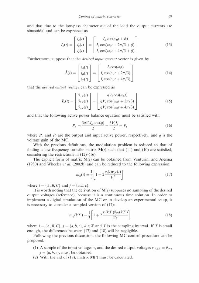
(3) Using (9), conducting times tij should be generated.(4) Nine pulses of duration tij must be generated, according to the pattern shown
in figure 2 for the jth output phase. Note that this corresponds to the genera-tion of the switching functions SijðtÞ (see (1)).
(5) The switching functions SijðtÞ must be used to turn on or off the bidirectionalswitches of the MC in an appropriate way.
With the previously discussed strategy, the output voltages of figure 3 aregenerated. Note that the figure shows only one output voltage with its reference;it can be appreciated that the output voltage has an important harmonic content dueto the switching synthesis principle. Figure 4 shows a detailed version of figure 3,which clearly demonstrates that the output voltage is synthesized using a temporalaverage of the input voltages: in one switching interval, denoted T in the figure, theoutput voltage switches among the three input voltages and the time that each ofthese voltages is applied to the output determines its contribution to the outputvoltage low-frequency component.
Note that, because of the averaging working principle, the output voltage low-frequency component cannot exceed the maximum available amplitudes for allinstants. The reference can attain its maximum at an arbitrary time, say, for example,t ¼ 1:7ms (see figure 4) and therefore the worst-case maximum available amplitudesare equal to 0.5Vi and, therefore, the voltage gain of the MC is restricted to be lessthan 0.5. It must be clarified, however, that this limit is small since the modulationunder consideration uses the phase-to-neutral voltages to synthesize the outputvoltages, i.e. this is a limitation arising from the modulation used, not from theMC. It is possible to use the line-to-line voltages or space vector modulation toincrease the maximum voltage gain to q¼ 0.866 (Huber et al. 1989, Huber andBorojevic 1995, Wheeler et al. 2002b).
0 0.5 1 1.5 2−0.5
00.5
11.5
SA
j
0 0.5 1 1.5 2−0.5
00.5
11.5
SB
j
0 0.5 1 1.5 2−0.5
00.5
11.5
SC
j
time [ms]
tAj
tBj
tCj
Figure 2. Switching functions of the jth output phase.
70 J. Rodrıguez et al.

4. Application issues
Before we describe the simulation strategy it is important to take note of two prob-lems that arise when implementing an MC in practice. These are the commutationproblem and the overvoltage problem.
1 1.5 2 2.5 3
x 10−3
−1
−0.8
−0.6
−0.4
−0.2
0
0.2
0.4
0.6
0.8
1
time [s]
ampl
itude
[p.u
.]
T
vA
vB
vC
vaN
ref
vaN
Figure 4. Working principle of an MC (detail of figure 3).
0 0.005 0.01 0.015 0.02
−1
−0.8
−0.6
−0.4
−0.2
0
0.2
0.4
0.6
0.8
1
time [s]
ampl
itude
[p.u
.]
vaN
refv
A
vB
vC
vaN
Figure 3. Typical output voltage of an MC (see text for nomenclature and details).
Control of matrix converter 71

4.1 The commutation problem
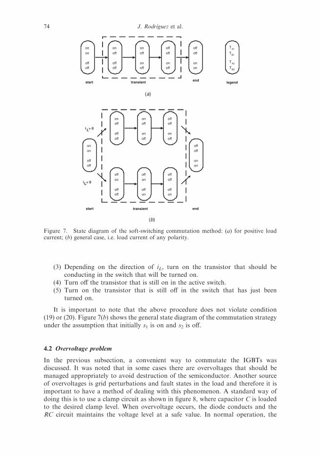
In order to approximate the behaviour of ideal bidirectional switches, manytechnically feasible solutions have been proposed, as shown in figure 5. We willconcentrate on the most popular one, and refer the interested reader to Wheeleret al. (2002a,b) and Mahlein et al. (2002b).
The considered solution uses the topology of figure 5(b) to implement a bidirec-tional switch. In figure 5(b) TA and TB are simply IGBT transistors and D1 and D2
are diodes. Due to D1 and D2, if both transistors are off there will be no currentcirculation; that is, the considered topology can block voltages of any polarity. If, forexample, V1 > V2, TA is on and TB is off, current will flow in the direction indicatedby figure 5(b). In the contrary case, i.e. if V1<V2, TB is on and TA is off, current willflow in the opposite direction. The previous characteristics make the presentedtopology a bidirectional switch.
It is worth noting that, although the topology of figure 5(b) is the basis of abidirectional switch, the time required to turn on or off an IGBT makes the com-mutation a nontrivial task. As an example of how the commutation actually takesplace, consider figure 6. It should be noted that in order to obey equation (2), thefollowing conditions should be avoided:
TA1 and TB2 on, with VA > VB
TA2 and TB1 on, with VA < VB
)ð19Þ
TA1 and TA2 off, with iL > 0
TB1 and TB2 off, with iL < 0
)ð20Þ
TA
V1
D1
D2
V2
TB
(a)
(b)
Figure 5. (a) Diode bridge bidirectional switch and (b) common emitter back-to-backbidirectional switch.
72 J. Rodrıguez et al.
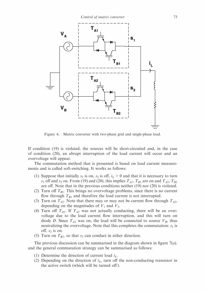
If condition (19) is violated, the sources will be short-circuited and, in the caseof condition (20), an abrupt interruption of the load current will occur and anovervoltage will appear.
The commutation method that is presented is based on load current measure-ments and is called soft-switching. It works as follows:
(1) Suppose that initially s1 is on, s2 is off, iL>0 and that it is necessary to turns1 off and s2 on. From (19) and (20), this implies TA1, TB1 are on and TA2, TB2
are off. Note that in the previous conditions neither (19) nor (20) is violated.(2) Turn off TB1. This brings no overvoltage problems, since there is no current
flow through TB1 and therefore the load current is not interrupted.(3) Turn on TA2. Note that there may or may not be current flow through TA2,
depending on the magnitudes of V1 and V2.(4) Turn off TA1. If TA2 was not actually conducting, there will be an over-
voltage due to the load current flow interruption, and this will turn ondiode D. Since TA2 was on, the load will be connected to source VB, thusneutralizing the overvoltage. Note that this completes the commutation: s1 isoff, s2 is on.
(5) Turn on TB2, so that s2 can conduct in either direction.
The previous discussion can be summarised in the diagram shown in figure 7(a).and the general commutation strategy can be summarised as follows:
(1) Determine the direction of current load iL.(2) Depending on the direction of iL, turn off the non-conducting transistor in
the active switch (which will be turned off ).
s1
s2
TB1
TA1
TB2
TA2
VA
VB
iL
s1
s2
TB1
TA1
TB2
TA2
VA
VB
iL
Figure 6. Matrix converter with two-phase grid and single-phase load.
Control of matrix converter 73
(3) Depending on the direction of iL, turn on the transistor that should beconducting in the switch that will be turned on.
(4) Turn off the transistor that is still on in the active switch.(5) Turn on the transistor that is still off in the switch that has just been
turned on.
It is important to note that the above procedure does not violate condition(19) or (20). Figure 7(b) shows the general state diagram of the commutation strategyunder the assumption that initially s1 is on and s2 is off.
4.2 Overvoltage problem
In the previous subsection, a convenient way to commutate the IGBTs wasdiscussed. It was noted that in some cases there are overvoltages that should bemanaged appropriately to avoid destruction of the semiconductor. Another sourceof overvoltages is grid perturbations and fault states in the load and therefore it isimportant to have a method of dealing with this phenomenon. A standard way ofdoing this is to use a clamp circuit as shown in figure 8, where capacitor C is loadedto the desired clamp level. When overvoltage occurs, the diode conducts and theRC circuit maintains the voltage level at a safe value. In normal operation, the
endstart
on
off
offoff
on
off
onoff
on
on
offoff
off
off
onoff
off
off
onon
transient legend
TA1
(a)
start
onoff
off
off
onoff
on
off
onon
offoff
offoff
on
off
offoff
onon
end
off
on
offoff
off
on
offon
off
off
offon
transient
i L> 0
iL< 0
(b)
TB1
TA2
TB2
Figure 7. State diagram of the soft-switching commutation method: (a) for positive loadcurrent; (b) general case, i.e. load current of any polarity.
74 J. Rodrıguez et al.

diodes are off and the clamp circuit has no influence on the MC operation. Itis important to note that the power level is very low for the clamp circuit(Klumpner et al. 2002b).
5. Simulation
The converter is simulated using the Matlab�–Simulink� package to demonstratethe basic principle of the MC for the student. Equation (18) is used to obtain theelements of the low-frequency transfer matrix MðtÞ and times tij . Figure 9 shows thegeneral structure of the module that generates the components mij of matrix MðtÞ,taking as inputs the current samples of the MC input voltages (vi) and of the desiredoutput voltages ( �vvjN ¼ vjREF).
The most important part of the simulation is the generation of the switchingfunctions of the bidirectional switches (SijðtÞ). These functions correspond to thegate drive signals of the power switches in the real converter. Figure 10 presentsthe block diagram used to generate these functions in the case of the jth outputphase. This block diagram is more easily understood if we consider thevariables and waveforms shown in figure 11, which corresponds to the following
LC- Filter
Grid(50 Hz)
LC- Filter
IM
Matrix converter
Diode clamp circuit
C R
Grid(50 Hz)
LC- Filter
IM
Matrix converter
Diode clamp circuit
C R
Grid(50 Hz)
Figure 8. Clamp circuit to manage overvoltages.
2
tij
1
mij
T
Samplinginterval
1/3
2
1/(Vi*Vi)
1
2
vjREF
1
viN
Figure 9. Generation of the duty cycle mij in the Matlab�–Simulink� software package.
Control of matrix converter 75
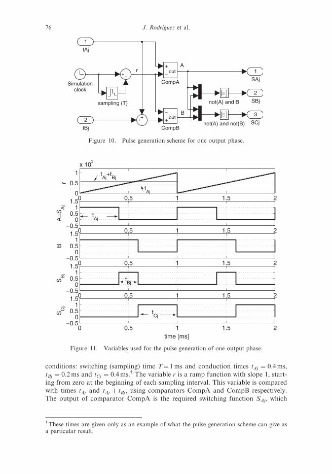
conditions: switching (sampling) time T¼ 1ms and conduction times tAj ¼ 0:4ms,tBj ¼ 0:2ms and tCj ¼ 0:4ms.y The variable r is a ramp function with slope 1, start-ing from zero at the beginning of each sampling interval. This variable is comparedwith times tAj and tAj þ tBj , using comparators CompA and CompB respectively.The output of comparator CompA is the required switching function SAj, which
rA
B 3
SCj
2
SBj
1
SAj
sampling (T)
not(A) and not(B)
not(A) and B
Simulationclock
−
+ out
CompB
+
− out
CompA
2
tBj
1
tAj
Figure 10. Pulse generation scheme for one output phase.
0 0.5 1 1.5 20
0.5
1x 10
3
r
0 0.5 1 1.5 2−0.5
00.5
11.5
A=
SA
j
0 0.5 1 1.5 2−0.5
00.5
11.5
B
0 0.5 1 1.5 2−0.5
00.5
11.5
SB
j
0 0.5 1 1.5 2−0.5
00.5
11.5
SC
j
time [ms]
tAj
tCj
tBj
tAj
+tBj
tAj
Figure 11. Variables used for the pulse generation of one output phase.
yThese times are given only as an example of what the pulse generation scheme can give asa particular result.
76 J. Rodrıguez et al.

corresponds to a pulse of amplitude 1 with a duration equal to tAj . The followinglogic decisions are used to generate the other switching functions:
SBj ¼ notðAÞ and B
SCj ¼ notðAÞ and notðBÞ
�ð21Þ
Figure 12 presents the block diagram used to generate the output voltages withrespect to the neutral N of the source. As expressed by (3), these voltages areobtained from the product of the input voltages and the switching functions.
In general, the neutral of the load n is isolated from the neutral of the source N.In order to calculate the output currents, it is necessary to obtain previously theoutput voltages of the MC with respect to neutral n (vjn). This is achieved by thefollowing equation:
vjn ¼ vjN � vnN , with j ¼ fa, b, cg ð22Þ
where the voltage between neutrals is obtained from
vnN ¼vaN þ vbN þ vcN
3ð23Þ
The load currents are obtained from voltages vjn using the following equation:
ijðsÞ
vjnðsÞ¼
1
Lsþ R, j ¼ fa, b, cg ð24Þ
where s is the Laplace operator and L ,R are the load parameters.Figure 13 presents in a clear form the block diagram corresponding to
equations (22)–(24), used to generate the different voltages and currents in theload. The currents at the input side of the MC are generated by the blocks offigure 14, which is based on equation (4).
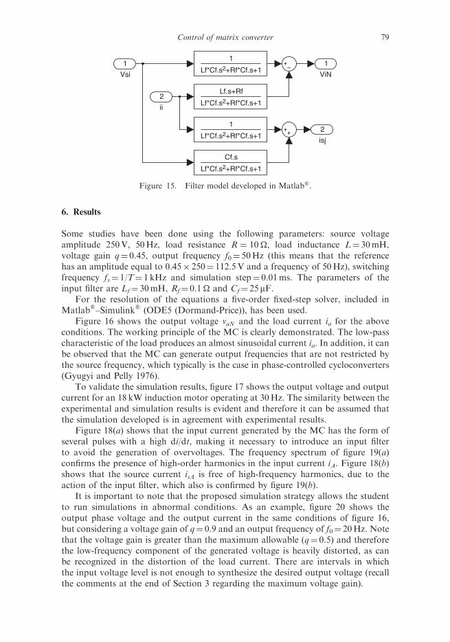
In order to make the link between the grid input voltages (vsi) and currents (isi)and the MC input voltages (vi) and currents (ii), the filter model presented in
1
vjN
6
SCj
5
SBj
4
SAj
3
vC
2
vB
1
vA
Figure 12. Generation of the output voltage of the jth phase.
Control of matrix converter 77

equations (5) and (7) must be considered. This is easily achieved by considering thetransfer function blocks of the Control System Toolbox of Matlab� (TheMathworks 1999), as shown in figure 15.
Finally, figure A.1 in the appendix presents the general block diagram of theMC simulation, where block 1 models the input filter, block 2 generates the switch-ing functions, blocks 3, 4 and 5 generate the output voltages vaN , vbN , vcN , block 6represents the load, generating its voltages and currents, and blocks 7, 8 and 9calculate the MC input currents iA, iB and iC.
VnN
6
vcn5
ic
4
vbn3
ib
2
van1
ia
1
L.s+Rload model
1
L.s+R
1
L.s+R
1/3
3
vcN
2
vbN
1
vaN
Figure 13. Generation of voltages and currents in the load.
1
ii
6
Sic
5
Sib
4
Sia
3
ic
2
ib
1
ia
Figure 14. Generation of the input currents in Matlab�.
78 J. Rodrıguez et al.
6. Results
Some studies have been done using the following parameters: source voltageamplitude 250V, 50Hz, load resistance R ¼ 10�, load inductance L¼ 30mH,voltage gain q¼ 0.45, output frequency f0¼ 50Hz (this means that the referencehas an amplitude equal to 0.45� 250¼ 112.5V and a frequency of 50Hz), switchingfrequency fs¼ 1/T¼ 1 kHz and simulation step¼ 0.01ms. The parameters of theinput filter are Lf¼ 30mH, Rf¼ 0.1� and Cf¼ 25 mF.
For the resolution of the equations a five-order fixed-step solver, included inMatlab�–Simulink� (ODE5 (Dormand-Price)), has been used.
Figure 16 shows the output voltage vaN and the load current ia for the aboveconditions. The working principle of the MC is clearly demonstrated. The low-passcharacteristic of the load produces an almost sinusoidal current ia. In addition, it canbe observed that the MC can generate output frequencies that are not restricted bythe source frequency, which typically is the case in phase-controlled cycloconverters(Gyugyi and Pelly 1976).
To validate the simulation results, figure 17 shows the output voltage and outputcurrent for an 18 kW induction motor operating at 30Hz. The similarity between theexperimental and simulation results is evident and therefore it can be assumed thatthe simulation developed is in agreement with experimental results.
Figure 18(a) shows that the input current generated by the MC has the form ofseveral pulses with a high di/dt, making it necessary to introduce an input filterto avoid the generation of overvoltages. The frequency spectrum of figure 19(a)confirms the presence of high-order harmonics in the input current iA. Figure 18(b)shows that the source current isA is free of high-frequency harmonics, due to theaction of the input filter, which also is confirmed by figure 19(b).
It is important to note that the proposed simulation strategy allows the studentto run simulations in abnormal conditions. As an example, figure 20 shows theoutput phase voltage and the output current in the same conditions of figure 16,but considering a voltage gain of q¼ 0.9 and an output frequency of f0¼ 20Hz. Notethat the voltage gain is greater than the maximum allowable (q¼ 0.5) and thereforethe low-frequency component of the generated voltage is heavily distorted, as canbe recognized in the distortion of the load current. There are intervals in whichthe input voltage level is not enough to synthesize the desired output voltage (recallthe comments at the end of Section 3 regarding the maximum voltage gain).
2
isj
1
ViN
1
Lf*Cf.s2+Rf*Cf.s+1
Cf.s
Lf*Cf.s2+Rf*Cf.s+1
Lf.s+Rf
Lf*Cf.s2+Rf*Cf.s+1
1
Lf*Cf.s2+Rf*Cf.s+1
2
ii
1
Vsi
Figure 15. Filter model developed in Matlab�.
Control of matrix converter 79

7. Conclusions
The working principle of the MC, controlled with the direct transfer functionapproach, has been presented. The modulation strategy and the most importantequations are clearly presented. In addition, an intelligent commutation strategyis explained, which avoids the generation of overvoltages and overcurrents.
0 0.01 0.02 0.03 0.04 0.05−400
−200
0
200
400
time [s]
v an [V
]
0 0.01 0.02 0.03 0.04 0.05−10
−5
0
5
10
time [s]
i a [A]
va REF
(a)
(b)
Figure 16. (a) Output voltage vaN , its reference (bold line), and (b) output current ia.
0 0.01 0.02 0.03 0.04 0.05−400
−200
0
200
400
time [s]
VaN
[V]
0 0.01 0.02 0.03 0.04 0.05−40
−20
0
20
40
time [s]
i a [A]
(a)
(b)
Figure 17. Waveforms for 18 kW induction motor drive at 415V, 50Hz input frequency,30Hz output frequency and sampling frequency of 2 kHz: (a) load voltage and (b) outputcurrent. (Experimental result.)
80 J. Rodrıguez et al.

0 0.01 0.02 0.03 0.04 0.05
−10
0
10
time [s]
i A [A
]
0 0.01 0.02 0.03 0.04 0.05
−10
0
10
time [s]
i sA [A
]v
sA
vsA
(a)
(b)
Figure 18. (a) Input current before the filter (THD¼ 120%) and (b) filtered input current(source current; THD¼ 14%).
0 1000 2000 3000 40000
0.5
1
frequency [Hz]
Rel
ativ
e am
plitu
de
0 1000 2000 3000 40000
0.5
1
frequency [Hz]
Rel
ativ
e am
plitu
de
(a)
(b)
Figure 19. (a) Spectrum of input current iA before filtering and (b) after the filter (sourcecurrent isA).
Control of matrix converter 81

In addition, the simulation of the MC controlled with the direct trans-fer function approach has been presented and clearly explained. The modelreproduces in a very good form the behaviour of the converter, including theeffect of the input filter. In addition, other aspects such as operation underabnormal conditions and overmodulation can be easily and directly simulated. It isimportant to note that the simulation results are in good agreement with experi-mental data.
The authors believe that, after studying this paper, students will clearly under-stand the most relevant issues of this attractive converter: safe commutation ofpower transistors, generation of overvoltages, advanced modulation methods andgeneration and filtering of harmonics. In this way, students get prepared to developmore advanced studies in the area of modern power converters.
Acknowledgment
The authors gratefully acknowledge the financial support provided by the ChileanResearch Fund FONDECYT (grant No. 1030368) and of the Universidad TecnicaFederico Santa Marıa.
Appendix
Figure A.1 shows the global simulation scheme as described in the text.
0 0.02 0.04 0.06 0.08 0.1−400
−200
0
200
400
time [s]
v an [V
]
0 0.02 0.04 0.06 0.08 0.1−20
−10
0
10
20
time [s]
i a [A]
(a)
(b)
va REF
Figure 20. (a) Output voltage vaN , its reference (bold line), and (b) output current iawith overmodulation.
82 J. Rodrıguez et al.

Ref
eren
ce
Hel
p:
q (v
olta
ge g
ain
<=
0.5
) fr
ec (
outp
ut fr
eque
ncy
in H
z) p
aso
(sim
ulat
ion
step
)h
(sam
plin
g in
terv
al)
L y
R (
load
par
amet
ers)
Lf, C
f Rf (
filte
r pa
ram
eter
s)
Grid
Vol
tage
gai
n
1
2
3, 4
, 5
6
7, 8
, 9
vj n
vj
isj
ij
iK
Wor
king
prin
cipl
e
iB
vcvb
vb_n
va_n
ij
iA
va
vK
vsa
isa
va_r
ef
iC
vc_n
t
vA vB vC va r
ef
vb r
ef
vc r
ef
SA
a
SB
a
SC
a
SA
b
SB
b
SC
b
SA
c
SB
c
SC
c
ia ib ic SK
a
SK
b
SK
c
iK
ia ib ic SK
a
SK
b
SK
c
iK
ia ib ic SK
a
SK
b
SK
c
iK
vA vB vC SA
j
SB
j
SC
j
vj
vA vB vC SA
j
SB
j
SC
j
vj
vA vB vC SA
j
SB
j
SC
j
vj
va N
vb N
vc N
ia ib icva
nvb
nvc
n
Load
circ
uit
Inpu
t cur
rent
and
sour
ce v
olta
ge
[iA]
[iB]
[iC]
[iC]
[iB]
[iA]
Vsc
ib
Vc
Isc
Filt
er C
Vsb
ib
Vb
Isb
Filt
er B
Vsa
ia
Va
Isa
Filt
er A
q
Clo
ck
Figure
A1.
Globalsimulationschem
eforthematrix
converter.
Control of matrix converter 83
References
S. Bernet, S. Ponnaluri and R. Teichmann, ‘‘Design and loss comparison of matrix convertersand voltage-source converters for modern AC drives’’, IEEE Transactions onIndustrial Electronics, 49, pp. 304–314, 2002.
F. Blaabjerg, D. Casadei, C. Klumpner and M. Matteini, ‘‘Comparison of twocurrent modulation strategies for matrix converters under unbalanced inputvoltage conditions’’, IEEE Transactions on Industrial Electronics, 49, pp. 289–296,2002.
L. Empringham, P. Wheeler and J. Clare, ‘‘Intelligent commutation of matrix converterbi-directional switch cells using novel gate drive techniques’’, in Proceedings ofIEEE PESC98, 1998, pp. 707–713.
L. Gyugyi and B. Pelly, Static Power Frequency Changers, New York: John Wiley, 1976.L. Huber and D. Borojevic, ‘‘Space vector modulated three-phase to three-phase matrix
converter with input power factor correction’’, IEEE Transactions on IndustrialElectronics, 31, pp. 1234–1246, 1995.
L. Huber, D. Borojevic and N. Burany, ‘‘Voltage space vector based PWM control offorced commutated cycloconverters’’, in Proceedings of IEEE IECON89, 1989,pp. 106–111.
C. Klumpner and F. Blaabjerg, ‘‘Experimental evaluation of ride-through capabilities for amatrix converter under short power interruptions’’, IEEE Transactions on IndustrialElectronics, 49, pp. 315–324, 2002.
C. Klumpner, P. Nielsen, I. Boldea and F. Blaabjerg, ‘‘A new matrix converter motor(MCM) for industry applications’’, IEEE Transactions on Industrial Electronics, 49,pp. 325–335, 2002a.
C. Klumpner, P. Nielsen, I. Boldea and F. Blaabjerg, ‘‘New solutions for a low-cost powerelectronic building block for matrix converters’’, IEEE Transactions on IndustrialElectronics, 49, pp. 336–344, 2002b.
J. Mahlein, M. Bruckmann and M. Braun, ‘‘Passive protection strategy for a drive systemwith a matrix converter and an induction machine’’, IEEE Transactions on IndustrialElectronics, 49, pp. 297–303, 2002a.
J. Mahlein, J. Igney, J. Weigold, M. Braun and O. Simon, ‘‘Matrix converter commutationstrategies with and without input voltage sign measurement’’, IEEE Transactions onIndustrial Electronics, 49, pp. 407–414, 2002b.
The Mathworks, Inc., Control System Toolbox for use with Matlab�, 1999.N. Mohan, T. Undeland and W. Robbin, Power Electronics, 2nd ed., New York:
John Wiley, 1995.P. Nielsen, F. Blaabjerg and J. Pedersen, ‘‘Novel solutions for protection of matrix converter
to three phase induction machine’’, in Conference Record of the IEEE–IAS AnnualMeeting, 1997, pp. 1447–1454.
J. Rodriguez, ‘‘A new control technique for AC–AC converters’’, in Proceedings ofIFAC Control in Power Electronics and Electrical Drives Conference, Lausanne(Switzerland), 1983, pp. 203–208.
J. Rodrıguez, ‘‘Guest editorial for the special section on matrix converters’’, IEEETransactions on Industrial Electronics, 49, pp. 274–275, 2002.
A. Trzynadlowski, Modern Power Electronics, New York: John Wiley, 1998.M. Venturini, ‘‘A new sine wave in sine wave out conversion technique which eliminates
reactive elements’’, Proceedings of POWERCON 7, E3, pp. 1–15, 1980.M. Venturini and A. Alesina, ‘‘The generalized transformer: A new bidirectional sinusoidal
waveform frequency converter with continuously adjustable input power factor’’,Proceedings of IEEE PESC80, pp. 242–252, 1980.
P. Wheeler, J. Clare, L. Empringham, M. Bland and M. Apap, ‘‘Gate drive level intelligenceand current sensing for matrix converter current commutation’’, IEEE Transactionson Industrial Electronics, 49, pp. 382–389, 2002a.
P. Wheeler, J. Rodrıguez, J. Clare, L. Empringham and A. Weinstein, ‘‘Matrix converters:A technology review’’, IEEE Transactions on Industrial Electronics, 49, pp. 276–288,2002b.
84 J. Rodrıguez et al.

E. Wiechmann, R. Burgos and J. Rodrıguez, ‘‘Continuously motor-synchronized ride-throughcapability for matrix-converter adjustable-speed drives’’, IEEE Transactions onIndustrial Electronics, 49, pp. 390–400, 2002.
J.H. Youm and B.H. Kuon, ‘‘Switching technique for current-controlled AC-to-ACconverters’’, IEEE Transactions on Industrial Electronics, 46, pp. 309–318, 1999.
Control of matrix converter 85