control of matrix converters - unibo.it · 5 preface a matrix converter (mc) is an array of...
TRANSCRIPT

University of Bologna
Final Dissertation in 2007
DEPARTMENT OF ELECTRICAL ENGINEERING FACULTY OF ENGINEERING
Ph. D. in Electrical Engineering XIX year
POWER ELECTRONICS, MACHINES AND DRIVES (ING-IND/32)
Control of Matrix Converters
Ph. D. Thesis: Tutor: Luca Zarri Prof. Giovanni Serra Ph. D. Coordinator: Prof. Francesco Negrini

1
Contents
CONTENTS..........................................................................................................1 PREFACE ............................................................................................................5
CHAPTER 1 .........................................................................................................8 FUNDAMENTALS OF MATRIX CONVERTERS ..............................................8
1.1. STRUCTURE OF MATRIX CONVERTER....................................................... 8 1.2. INPUT CURRENT MODULATION STRATEGIES .......................................... 14 1.3. INSTABILITY PHENOMENA....................................................................... 16 1.4. COMPARISON BETWEEN MC AND BACK-TO-BACK CONVERTER.............. 19 1.5. CONCLUSION........................................................................................... 23
CHAPTER 2 .......................................................................................................25 MODULATION STRATEGIES..........................................................................25
2.1. INTRODUCTION ....................................................................................... 25 2.2. DUTY-CYCLE MATRIX APPROACH .......................................................... 27 2.3. SPACE VECTOR APPROACH .................................................................... 30 2.4. NEW DUTY-CYCLE SPACE VECTOR APPROACH...................................... 37 2.5. GENERALIZED MODULATION STRATEGY................................................. 40 2.6. COMPARISON OF THE MODULATION STRATEGIES ................................... 44 2.7. CONCLUSION........................................................................................... 49
CHAPTER 3 .......................................................................................................51 ADVANCED MODULATION STRATEGIES....................................................51
3.1. INTRODUCTION ....................................................................................... 52 3.2. DUTY-CYCLE SPACE VECTOR APPROACH .............................................. 53

2
3.3. GENERALIZED MODULATION STRATEGY................................................. 55 3.4. MODULATION STRATEGY WITH MINIMUM BSOS .................................... 57 3.5. SIMULATION RESULTS............................................................................. 59 3.6. PRELIMINARY CONCLUSION .................................................................... 61 3.7. OPTIMISATION OF SVM: AN OVERVIEW ................................................. 63 3.8. SVM FOR MCS ....................................................................................... 65 3.9. ANALYSIS OF THE LOAD CURRENT RIPPLE............................................. 68 3.10. OPTIMAL SPACE VECTOR MODULATION STRATEGY........................... 70 3.11. SIMULATION RESULTS......................................................................... 74 3.12. EXPERIMENTAL RESULTS.................................................................... 75 3.13. CONCLUSION....................................................................................... 76
CHAPTER 4 .......................................................................................................78 STABILITY OF MATRIX CONVERTER .........................................................78
4.1. INTRODUCTION ....................................................................................... 79 4.2. MATHEMATICAL MODEL USING L-C FILTER........................................... 80 4.3. STEADY-STATE OPERATING CONDITIONS............................................... 82 4.4. STABILITY ANALYSIS .............................................................................. 83 4.5. MATHEMATICAL MODEL USING R-L-C FILTER....................................... 85 4.6. SIMULATION RESULTS............................................................................. 87 4.7. USE OF A DIGITAL INPUT FILTER ........................................................... 90 4.8. STABILITY ANALYSIS .............................................................................. 94 4.9. ANALYSIS OF THE OUTPUT VOLTAGE DISTORTION ................................ 96 4.10. COMPUTER SIMULATIONS OF A MC WITH INPUT DIGITAL FILTER ..... 97 4.11. IMPORTANT REMARKS ABOUT STABILITY ........................................ 104 4.12. CONCLUSION..................................................................................... 107
CHAPTER 5 ..................................................................................................... 109 ADVANCED MODELS FOR STABILITY ANALYSIS ................................... 109
5.1. INTRODUCTION ..................................................................................... 109 5.2. INPUT/OUTPUT MATRIX CONVERTER PERFORMANCE ......................... 111 5.3. STEADY-STATE OPERATING CONDITIONS WITH BALANCED AND
SINUSOIDAL SUPPLY VOLTAGES ............................................................................ 114 5.4. SMALL SIGNAL EQUATIONS ................................................................... 115 5.5. STABILITY ANALYSIS ............................................................................ 118 5.6. SMALL SIGNAL EQUATIONS INTRODUCING A DIGITAL FILTER .............. 121 5.7. MODEL FOR THE MC LOSSES................................................................ 123 5.8. SIMULATION RESULTS........................................................................... 127

3
5.9. EXPERIMENTAL RESULTS...................................................................... 131 5.10. STABILITY ANALYSIS BASED ON A LARGE SIGNAL MODEL ............... 133 5.11. EQUATIONS OF THE SYSTEM ............................................................. 134 5.12. STABILITY ANALYSIS ........................................................................ 139 5.13. DELAY OF THE DIGITAL CONTROL ................................................... 144 5.14. IMPROVEMENT OF THE STABILITY POWER LIMIT ............................. 148 5.15. EXPERIMENTAL RESULTS.................................................................. 149 5.16. CONCLUSION..................................................................................... 154
CHAPTER 6 ..................................................................................................... 156 QUALITY OF THE INPUT CURRENT.......................................................... 156
6.1. INTRODUCTION ..................................................................................... 157 6.2. INPUT AND OUTPUT UNBALANCE REPRESENTATION ........................... 158 6.3. CONSTANT DISPLACEMENT ANGLE BETWEEN INPUT VOLTAGE AND
CURRENT VECTORS (METHOD 1).......................................................................... 159 6.4. VARIABLE DISPLACEMENT ANGLE BETWEEN INPUT VOLTAGE AND
CURRENT VECTORS (METHOD 2).......................................................................... 163 6.5. NUMERICAL SIMULATIONS .................................................................... 165 6.6. UNBALANCED OUTPUT CONDITIONS..................................................... 166 6.7. BALANCED OUTPUT CONDITIONS ......................................................... 167 6.8. PRELIMINARY CONCLUSIONS................................................................. 171 6.9. INTRODUCTION TO THE GENERAL ANALYSIS OF THE INPUT CURRENT 172 6.10. BASIC EQUATIONS ............................................................................ 173 6.11. SMALL-SIGNAL EQUATIONS IN THE FOURIER DOMAIN ...................... 176 6.12. DETERMINATION OF THE INPUT VOLTAGE ....................................... 177 6.13. EXPRESSION OF THE INPUT VOLTAGE IN TERMS OF HARMONICS ..... 179 6.14. EXPERIMENTAL RESULTS.................................................................. 180 6.15. CONCLUSION..................................................................................... 184
CHAPTER 7 ..................................................................................................... 186 ELECTRIC DRIVES ........................................................................................ 186
7.1. INTRODUCTION ..................................................................................... 186 7.2. MACHINE EQUATIONS ........................................................................... 189 7.3. MAXIMUM TORQUE CAPABILITY IN THE FIELD WEAKENING REGION.. 191 7.4. CONTROL ALGORITHM.......................................................................... 193 7.5. FIELD WEAKENING ALGORITHM........................................................... 196 7.6. FLUX AND TORQUE OBSERVERS ........................................................... 199 7.7. SIMULATION RESULTS........................................................................... 200

4
7.8. EXPERIMENTAL RESULTS...................................................................... 203 7.9. CONCLUSION......................................................................................... 206
APPENDIX A................................................................................................... 208
APPENDIX B ................................................................................................... 211
APPENDIX C................................................................................................... 212
APPENDIX D................................................................................................... 213
APPENDIX E ................................................................................................... 214
APPENDIX F ................................................................................................... 215
APPENDIX G................................................................................................... 217 REFERENCES ................................................................................................. 218
5
Preface
A matrix converter (MC) is an array of controlled semiconductor switches
that directly connect each input phase to each output phase, without any
intermediate dc link.
The main advantage of MCs is the absence of bulky reactive elements,
that are subject to ageing, and reduce the system reliability. Furthermore,
MCs provide bidirectional power flow, nearly sinusoidal input and output
waveforms and controllable input power factor. Therefore MCs have received
considerable attention as a good alternative to voltage-source inverter (VSI)
topology.
The development of MCs started when Alesina and Venturini proposed
the basic principles of operation in the early 1980’s [1].
Afterwards the research in this fields continued in two directions. On the
one hand there was the need of reliable bidirectional switches, on the other
hand the initial modulation strategy was abandoned in favor of more modern
solutions, allowing higher voltage transfer ratio and better current quality.
In the original Alesina and Venturini’s theory the voltage transfer ratio
was limited to 0.5, but it was shown later that, by means of third harmonic
injection techniques, the maximum voltage transfer ratio could be increased
up to 0.866, a value which represents an intrinsic limitation of three-phase
MCs with balanced supply voltages [2].
A new intuitive approach towards the control of matrix converters, often

6
defined “indirect method”, was presented in [3]. According to this method the
MC is described as a virtual two stage system, namely a 3-phase rectifier and
a 3-phase inverter connected together through a fictitious DC-link. The
indirect approach has mainly the merit of applying the well-established space
vector modulation (SVM) for VSI to MCs, although initially proposed only
for the control of the output voltage [4]. The SVM was successively
developed in order to achieve the full control of the input power factor, to
fully utilize the input voltages and to improve the modulation performance
[5], [6].
A general solution of the modulation problem for MCs was presented in
[7], based on the concept of “Duty-Cycle Space Vector”, that allows an
immediate comprehension of all the degrees of freedom that affect the
modulation strategies.
Meanwhile, several studies were presented about the bidirectional switches
necessary for the construction of a matrix converter. The bidirectional
switches were initially obtained combining discrete components [8]. Then, as
the interest toward matrix converter increased, some manufacturers produced
power modules specifically designed for matrix converter applications [9]. As
regards the hardware components, the switches are usually traditional silicon
IGBTs, but also other solutions have been recently tested, such as MCTs or
IGBTs with silicon carbide diodes. The performance of the switches has been
compared in [10]-[13].
Another problem that the researchers have dealt with is the current
commutation between the bidirectional switches. The absence of free-
wheeling diodes obliges the designer to control the commutation in order to
avoid short circuits and over voltages. A comparison among several solutions
has been done in [14], [15] and [16].
To obtain a good performance of the matrix converter, it is necessary also
the design of a L-C filter to smooth the input currents and to satisfy the EMI
requirements [17]. It has been shown that the presence of a resonant L-C
filter could determine instability phenomena that can prevent the matrix
converter to deliver the rated power to the load [18]. A possible remedy for
this problem consists in filtering the input voltage before calculating the
duty-cycles. In this way it is possible to increase the stability power limit and
to obtain the maximum voltage transfer ratio.

7
All this aspects are considered in the next chapters. In particular, Chapter
1 gives an overview of the basic principles of matrix converters. Chapter 2
summarises the most important modulation strategies for matrix converter,
whereas Chapter 3 proposes two novel modulation techniques that allows
obtaining a better performance in terms of number of commutations and
current distortion.
Chapter 4 and 5 concern the stability problem. In those Chapters the
unstable behaviour of matrix converter is explained and some solutions are
proposed.
Chapter 6 analyses in details the quality of the input currents. Finally,
Chapter 7 presents and assesses a complete electric drive for induction motor
based on matrix converter.

8
1.Chapter 1 Fundamentals of Matrix Converters Abstract
The matrix converter has several attractive features and some companies
have shown a particular interest in its commercial exploitation. These
chapter presents an introduction to its technology and theory. After a brief
historical review, the basic hardware solutions for the development of matrix
converters are described. A notable part of the chapter is dedicated to the
comparison between matrix converter and back-to-back converter.
1.1. Structure of Matrix Converter
Basically, a matrix converter (MC) is composed by 9 bidirectional
switches, as shown in Fig. 1.1, where each dot of the grid represents a
connection between the output and the input terminals.
The converter is usually fed at the input side by a three phase voltage
source and it is connected to an inductive load at the output side.
The schematic circuit of a matrix converter feeding a passive load is
shown in Fig. 1.2. The system is composed by the voltage supply, an L-C
input filter, the MC and a load impedance.

9
A. Input Filter
The input filter is generally needed to smooth the input currents and to
satisfy the EMI requirements. A reactive current flows through the input
filter capacitor, leading to a reduction of the power factor, especially at low
output power. As a consequence, the capacitor is chosen in order to ensure at
least a power factor of 0.8 with 10% of the rated output power. After the
selection of the capacitor, the input filter inductance of the matrix converter
can be chosen in order to satisfy the IEEE Recommended Practices and
Requirements for Harmonic Control in Electrical Power Systems (IEEE Std.
519-1992).
B. Bidirectional Switches
The MC requires bidirectional switches with the capability to block the
Power Circuits
Input voltages
Output currents
Control System
Commutation control
IoIi Iline Rs Ls
Lf Cf
LLRLE
Fig. 1.2 - Complete scheme of a MC system.
3ii
03oi
2ii
3iv
1oi 2oi
1ii
3ov
2iv
33S
1ov 2ov
1iv 11S
12S
13S
21S
22S
23S
31S
32S
Input phase (a)
(b)
(c)
Output phase (A) (B) (C)
Fig. 1.1 - Basic scheme of matrix converters.

10
voltage and to conduct the current in both directions. There are two main
topologies for bi-directional switches, namely the common emitter anti-
parallel IGBT configuration and the common collector anti-parallel IGBT
configuration.
The common emitter arrangement is represented in Fig. 1.3(a). As can be
seen, two IGBTs are connected with two diodes in an anti-parallel
configuration. The diodes provide the reverse blocking capability.
The complete connection scheme of the common emitter arrangement is
shown in Fig. 1.4. The main advantage of this solution is that the two IGBTs
can be driven with respect the same point, i.e. the same common emitter,
that can be considered as a local ground for the bidirectional switch. On the
other hand, each bidirectional switch requires an insulated power supply, in
order to ensure a correct operation and, hence, a total of nine insulated
power supplies is needed. The power supplies must be insulated because, as a
bidirectional switch is turned on, the common emitter assumes the potential
of an input phase. Therefore, it is not possible for all the bidirectional
switches to be driven with respect to the same common point.
a) b)
Fig. 1.3 - Bidirectional switches. (a) common emitter configuration. (b) common collector configuration.
bc
B C
S11 S12 S13 S 23 S22 S21 S31 S32 S 33
a bc
A
S11 S12 S13 S 23 S22 S21 S31 S32 S 33
a
Fig. 1.4 - Complete scheme of the power stage using common emitter arrangement.
11
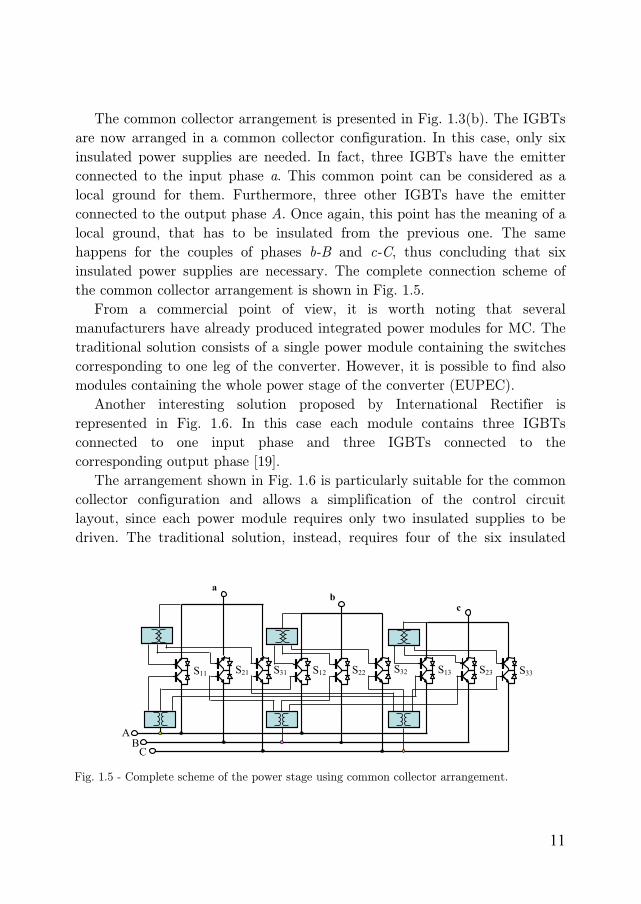
The common collector arrangement is presented in Fig. 1.3(b). The IGBTs
are now arranged in a common collector configuration. In this case, only six
insulated power supplies are needed. In fact, three IGBTs have the emitter
connected to the input phase a. This common point can be considered as a
local ground for them. Furthermore, three other IGBTs have the emitter
connected to the output phase A. Once again, this point has the meaning of a
local ground, that has to be insulated from the previous one. The same
happens for the couples of phases b-B and c-C, thus concluding that six
insulated power supplies are necessary. The complete connection scheme of
the common collector arrangement is shown in Fig. 1.5.
From a commercial point of view, it is worth noting that several
manufacturers have already produced integrated power modules for MC. The
traditional solution consists of a single power module containing the switches
corresponding to one leg of the converter. However, it is possible to find also
modules containing the whole power stage of the converter (EUPEC).
Another interesting solution proposed by International Rectifier is
represented in Fig. 1.6. In this case each module contains three IGBTs
connected to one input phase and three IGBTs connected to the
corresponding output phase [19].
The arrangement shown in Fig. 1.6 is particularly suitable for the common
collector configuration and allows a simplification of the control circuit
layout, since each power module requires only two insulated supplies to be
driven. The traditional solution, instead, requires four of the six insulated
C
S11 S12 S13 S23 S22S21 S31 S32
bc
S33
a
B A
Fig. 1.5 - Complete scheme of the power stage using common collector arrangement.

12
voltages that are necessary for the common collector configuration [20].
C. Current Commutation
Matrix converters have not free-wheeling diodes, unlike traditional voltage
source inverters. This makes the current commutation between switches a
difficult task, because the commutation has to be continuously controlled.
The switches have to be turned on and turned off in such a way as to avoid
short circuits and sudden current interruptions.
Many commutation strategies have been already studied. The most
common solution is the ”4-step commutation”, that requires information
about the actual current direction in the output phases. The four step
sequence is shown in Fig. 1.7, that refers to the general case of current
commutation from a bidirectional switch a to a bidirectional switch b.
In the beginning both IGBT of switch a are enabled. In the first step, the
San Sa
Sap Sbn
SbSbp
Io
a
b
San Sa
Sap
Sbn
SbSbp
Io
a
b
San Sa
Sap
Sbn
SbSbp
Io
a
b
San Sa
Sap
Sbn
SbSbp
Io
a
b
Step 1 Step 2 Step 3
San Sa
Sap Sbn
Sb Sbp
Io a
b
Step 4
Fig. 1.7 - Four step commutation sequence.
a
A
Input phases
Output phases
Fig. 1.6 - Scheme of the power stage based on modules manufactured by International Rectifier Corporation.

13
IGBT San, which is not conducting the load current, is turned off. In the
second step, the IGBT Sbp, that will conduct the current, is turned on. As a
consequence, both switches a and b can conduct only positive currents and
short circuits are prevented. Depending upon the instantaneous input
voltages, after the second step, the conducting diode of switch a is subject to
the voltage vab. If vab < 0, then the diode is reverse biased and a natural
commutation takes place. Otherwise, if vab ≥ 0, a hard commutation happens
when, in the third step, IGBT Sap is turned off. Finally, in the fourth step,
the non-conducting switch Sbn is enabled to allow the conduction of negative
currents. During a period of the input voltage, the natural commutation
occurs in 50% of all commutations and therefore this current commutation
has earned the name “semisoft switching”. Apart the 4-step commutation, other commutation strategies have been
proposed. In particular, a “3-step commutation strategy” is described in [14]
and [15]. The basic principle is that, combining the measurements of the
input voltages to those of the output currents, the control logic can always
perform the current commutation avoiding one step. In this way the
commutation time is reduced and the current quality improves.
D. Converter Protections
Due to the lack of free-wheeling paths for the currents, a number of
protection strategies should be adopted to prevent the damage of the
converter. Protections against over-load, short-circuit and over-voltage are
usually implemented.
The over-load protection is performed directly by the control logic, that
turns off all the switches when the load current is greater than the rated one.
This solution is not satisfactory in order to avoid the damage of the switches
if a load short-circuit happens, because the latency time of the DSP
depending on the cycle period is too high. Therefore, the protection against
the short circuit consists in the monitoring of the collector-emitter voltage of
all the IGBTs comprised in the power modules.
It is worth noting that it is not possible to simply turn off all the switches,
otherwise the inductive load current have no closing path. The most common
solution to this problem is to add a diode bridge clamp across the input and
the output sides of the converter, shown in Fig. 1.8. The small capacitor of

14
the clamp is designed to store the energy corresponding to the inductive load
current.
In addition the voltage across the capacitor is continuously measured. In
fact fault conditions are more frequently caused by instability phenomena at
the input of the converter or wrong switch commutations rather than short
circuits of the load. When the voltage across the capacitor becomes greater
than a limit value, the over-voltage protection should stop the converter.
It is possible to show that some diodes of the clamp can be replaced by
the diodes already present in the bidirectional switches if they are connected
in the common-emitter configuration. In this way, instead of 12 clamp diodes,
only 6 diodes are necessary. However, this solution requires three additional
insulated voltage supplies for the drivers to guarantee a correct operation.
Further details can be found in [17].
Another protection issue is that MC is less immune to power grid
disturbances than other converter. In hoisting applications, short-term
braking capability during a power outage is needed until the mechanical
brake engages or to perform a more effective combined braking.
A method to provide short-term braking capability during a power outage
for MCs was presented in [20]. It includes a braking chopper in the clamp
circuit, which allows a notable reduction of the capacitor size. The power
flow in the clamp circuit is reduced by increasing the harmonic content in the
motor currents, thus causing higher motor losses.
1.2. Input Current Modulation Strategies
The MC allows the control not only of the output voltages, but also of the
phase angle of the input current vector.
There are several possible solutions for the modulation of the input
current vector that basically differ in the direction along which the current
abc
ABC
Cclamp
Fig. 1.8 - Clamp circuit for the protection of the matrix converter.

15
vector is modulated. This direction can be represented introducing the vector
ψ with arbitrary magnitude, here named modulation vector. For any
strategy it is
0=⋅ψ iij (1.1)
where ii is the input current vector.
Any input current modulation strategy is completely defined once the
modulation vector ψ is known. In fact, the input current can be expressed as
a function of the modulation vector, the power absorbed by the converter
and the input voltage.
The power absorbed by the converter can be written as follows:
iii ivp ⋅=2
3. (1.2)
Then, combining (1.1) and (1.2) leads to the following expression of the
input current vector:
ψψ⋅
= v
pi
i
ii
3
2 (1.3)
where pi is the power delivered to the load.
If the switches are assumed ideal and the converter power losses are
neglected, the input power is equal to the power delivered to the load po. As
a consequence, (1.3) becomes as follows:
ψψ⋅
= v
pi
i
oi
3
2. (1.4)
As can be seen from (1.4) the input current space vector depends on the
output power level, the input voltage vector and the modulation vector.
The simplest input current modulation strategy (Strategy A) is to
maintain the input current vector in phase with the actual input voltage
vector, determining instantaneous unity input power factor. For instance,
Fig. 1.9 shows the behaviour of a 10-kW matrix converter. As is possible to
see, the line current is nearly sinusoidal and is kept in phase with the input
line-to-neutral voltage.

16
In case of input voltage disturbances, Strategy A produces non-sinusoidal
input currents having the lowest total RMS value.
In [21] it has been demonstrated that a better performance in terms of
input current distortion can be achieved if the input current vector is
dynamically modulated around the input voltage vector (Strategy B), or is
modulated to be in phase with the positive sequence fundamental component
of the input voltage vector (Strategy C). Theoretical and experimental results
obtained comparing these input current modulation strategies are given in
[22] and [23]. As a conclusion, it can be noted that Strategy B has to be
preferred in the case of unbalanced sinusoidal input voltages because allows
unbalanced, but sinusoidal, input currents to be obtained. Strategy C
performs better in presence of input voltage distortions. It is possible to
demonstrate that Strategy C represents the optimal modulation strategy
which determines the lowest total RMS value of the input current
disturbance. It will be pointed out that Strategy C has also a stabilizing
effect on the converter operation. This aspect will be clarified in the next
paragraph.
1.3. Instability Phenomena
The simplest modulation strategy is based on detecting the zero crossing
Fig. 1.9 - Experimental tests: stable steady state operation. Upper track: line current (20A/div). Middle track: input line-to-neutral voltage (400 V/div). Lower track: load line-to-line voltage (600 V/div).

17
of one input voltage for synchronizing the input current modulation. This
control technique performs correctly if an ideal power supply is assumed (i.e.
balanced and sinusoidal supply voltages), but in presence of input voltage
disturbances, these are reflected on the output side determining low order
voltage harmonics, as the matrix converter has no internal energy storage.
Considering unbalanced non-sinusoidal input voltages, the magnitude and the
angular velocity of the input voltage vector are not constant. Then, a simple
synchronization with the input voltages is no longer applicable but the input
voltages must be measured at each cycle period, in order to calculate the
duty-cycles necessary to generate balanced and sinusoidal output voltages.
However, the compensation of the input voltage disturbances leads to a
closed loop control that might cause instability phenomena when the matrix
converter output power exceeds a limit value. Typical waveforms of the line
current, the output voltage and the input line-to-line voltage during unstable
operation are shown in Fig. 1.10 for a 10-kW MC.
Here is a qualitative explanation of the instability phenomena. Let’s suppose that a voltage disturbance is temporarily applied to the converter
input, thus leading to a variation of the input current. It is worth noting that
this current variation is proportional to the output power. The current
harmonics with frequencies close to the resonant frequency of the LC input
Fig. 1.10 - Experimental test: unstable steady state operation. Upper track: line current(10A/div). Middle track: line to line output voltage (400 V/div). Lower track: line to lineinput voltage (400 V/div).
18
filter are amplified and their effect is to reinforce the input voltage
disturbance. If the output power is small, this reinforcement action is weak
and after the disturbance has vanished, the converter returns to the normal
steady state operation. Otherwise, if the output power is high enough, the
reinforcement action is sufficient to establish self-sustained oscillations in the
input voltages, even after the initial disturbance has vanished. In this case,
the system reaches a new steady state operation, but the converter does not
work correctly, because the input currents and voltages are remarkably
distorted.
It is interesting to note that these oscillations have the form of “beatings”, namely they are composed by at least two separate harmonics with close
frequencies.
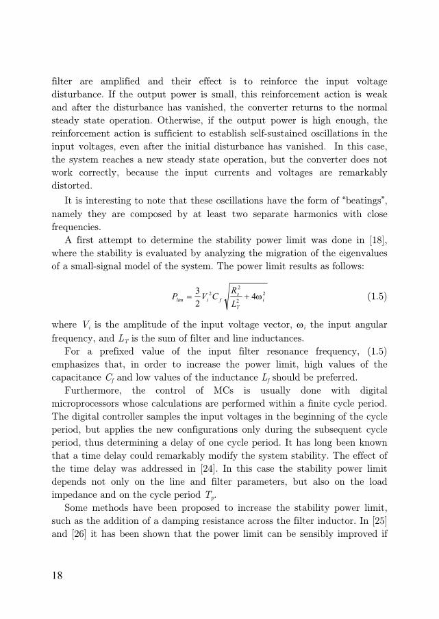
A first attempt to determine the stability power limit was done in [18],
where the stability is evaluated by analyzing the migration of the eigenvalues
of a small-signal model of the system. The power limit results as follows:
22
22 4
23
iT
sfilim L
RCVP ω+= (1.5)
where Vi is the amplitude of the input voltage vector, ωi the input angular
frequency, and LT is the sum of filter and line inductances.
For a prefixed value of the input filter resonance frequency, (1.5)
emphasizes that, in order to increase the power limit, high values of the
capacitance Cf and low values of the inductance Lf should be preferred.
Furthermore, the control of MCs is usually done with digital
microprocessors whose calculations are performed within a finite cycle period.
The digital controller samples the input voltages in the beginning of the cycle
period, but applies the new configurations only during the subsequent cycle
period, thus determining a delay of one cycle period. It has long been known
that a time delay could remarkably modify the system stability. The effect of
the time delay was addressed in [24]. In this case the stability power limit
depends not only on the line and filter parameters, but also on the load
impedance and on the cycle period Tp.
Some methods have been proposed to increase the stability power limit,
such as the addition of a damping resistance across the filter inductor. In [25]
and [26] it has been shown that the power limit can be sensibly improved if

19
the calculation of the duty-cycles is carried out by filtering the matrix
converter input voltages of the MC by means of a digital low-pass filter. For
example, the continuous-time equation of a possible filter applied to the input
voltage vector is the following one:
( )
ττω−−
= ifiiif vjv
dt
vd 1 (1.6)
where ifv is the filtered input voltage vector.
By increasing the time constant τ of the low-pass filter is possible to
increase the limit voltage. The only drawback is that the filter may affect to
some extent the capability of the control system to compensate the effect of
input voltage disturbances on the load currents.
1.4. Comparison between MC and Back-to-back Converter
To obtain the favours of market, MC should overcome the performance of
the other competitors in terms of cost, size and reliability. The most
important alternative to MC is the back-to-back converter, whose scheme is
shown in Fig. 1.11.
The MC has been already compared with the back-to-back converter
obtaining some important but not conclusive results. The comparison is
extremely difficult due to the high number of system parameters (i.e. input
filter and load parameters, switching frequency, output frequency,
Input voltage
Input current
Control System
Cf
Lf Lline Rline
3INV DC/ACAC/DC
Cdc
SVM Control
SVM Control
Fig.1.11 - Schematic drawing of the back-to-back converter.

20
modulation strategies, etc.) and to the inherent differences between the two
converter topologies, such as the maximum voltage transfer ratio. For
instance, the MC is able to generate balanced and sinusoidal output voltages,
whose amplitude can be regulated from zero to approximately 87% of the
input voltage amplitude. The output voltage of the back-to-back converter
instead is related to the DC-link voltage, and can be equal or even greater
than the input voltage [26].
The switching frequencies of the two converters are related to the adopted
modulation strategies and should be chosen with care in order to make a fair
comparison. Furthermore, both converters need an input filter to reduce the
input current harmonics, and the filter parameters are strictly related to the
switching frequency.
In [27]- [28] the comparison between the two topologies is performed in
terms of total switch losses, by evaluating the converter efficiency for given
operating conditions. On the other hand, it has been clearly emphasized that
in matrix converters the switch losses are not equally shared among the
switches, being the distribution related to the output frequency. Thus,
considering only the total switch losses as the key-parameter for the
comparison may be misleading.
In [29] the comparison between matrix and back-to-back converters is
performed by evaluating the maximum output power that each converter is
able to deliver to the load for different output frequency. The comparison is
carried out assuming the same types of IGBTs and diodes for both
converters. The maximum output power is determined taking into account
the thermal limit of each switch on the basis of a thermal model. All the
parameters needed for the comparison are shown in Tab. 1.1.
The performance of the two converter topologies has been tested for
different values of the output frequency in the range 0-150 Hz. The voltage
has been changed with the frequency according to the well-known constant
V/Hz law for induction motor drives. Thus, the output voltage is varied
proportionally to the frequency until 50Hz. For higher frequencies the phase
to phase output voltage is kept constant, i.e. 330V and 380V for the MC and
the back-to-back converter respectively. At low frequencies, the output
voltage has been changed in order to compensate the voltage drop on the
stator winding resistance.

21
The maximum output power achievable by the two converters as a
function of the output frequency is summarized in Fig. 1.12. It is evident that
the output power of MC is always higher than that of back-to-back
converter, showing a decrease around 50 and 100 Hz.
Fig. 1.13 shows the load current corresponding to the maximum output
power as a function of the output frequency, for the matrix and the back-to-
back converters. In this figure the better performance of the matrix converter
in terms of maximum output current is evident, especially in the low output
frequency range. The reason of so low values of the output current for the
back-to back converter is that, at low frequency, the output current is not
equally shared among the six switches. This situation is similar to the one
occurring when the matrix converter operates at 50 Hz. On the contrary, the
matrix converter is able to deliver high currents at low frequency because
these currents are equally shared among the 18 switches.
In order to make a fair comparison, one should take into account that the
TABLE 1.1 – SYSTEM PARAMETERS
Parameters Back to Back Matrix Converter
VIN 380 V(RMS), 50 Hz 380 V(RMS), 50 Hz
Rline 0.11Ω 0.11Ω
Lline 0.167mH 0.167mH
VDC 600V -
CDC 200μF -
Cf 25μF (Y) 40 μF (Y)
Lf 1.00 mH 0.35 mH
Rjc 0.64 °C/W 0.64 °C/W
Cj 31.2 mJ/°C 31.2 mJ/°C
θcase 70flC 70flC
fsw 6.6kHz (ac-dc),16kHz (dc-ac) 8kHz
cos ϕ load 0.8 0.8
Vout f out< 50 Hz , const. V/Hz
f out> 50 Hz , Vout = 380 V
f out< 50 Hz , const. V/Hz
f out> 50 Hz, Vout = 330 V
Diodes HFA16PB120 HFA16PB120
IGBTs IRG4PH50U IRG4PH50U

22
two converter topologies are realized with a different number of switches (i.e.
18 for the matrix converter and 12 for the back-to-back converter). For this
purpose two more significant quantities have been introduced, which rep-
resent the maximum output power per switch and the corresponding output
current per switch. These new quantities are represented in Figs. 1.14 and
1.15 respectively.
Fig. 1.14 shows that the output power per switch of the MC is always
lower than that of back-to-back converter, except for frequency values
ranging from 0 to about 30 Hz. On the other hand, it can be seen from Fig.
1.15 that the load current per switch of the matrix converter is always higher
than that of the back-to-back converter, except for frequency values around
50 Hz.
From Figs. 1.14 and 1.15 it can be concluded that in terms of maximum
0
5
10
15
20
25
30
35
0 25 50 75 100 125 150
Pout [kW]
fout [Hz]
mtxb2b
Fig. 1.12 - Maximum output power as a function of the output frequency.
0
10
20
30
40
50
60
70
80
0 25 50 75 100 125 150
mtxb2b
fout [Hz]
Iout [A]
Fig. 1.13 - Maximum output current as a function of the output frequency.

23
output power per switch the two converter topologies show practically the
same performance, whereas in terms of output current per switch the matrix
converter should be preferred to the back-to-back converter particularly in
the low output frequency range.
These results could be usefully employed in the choice of the converter
topology for drive systems, once the operating conditions and the over-load
capability were specified in details.
1.5. Conclusion
MCs provides some interesting features, such as compactness and
sinusoidal waveform of the input and output currents. However, there are
some potential disadvantages of MC technology that have so far prevented
its commercial exploitation. During the last two decades, several of these
problems were solved. In particular, the commutation problem between two
bidirectional switches was solved with the development of multistep
0
0,4
0,8
1,2
1,6
2
0 25 50 75 100 125 150
mtx b2b
switches
out
nP [kW]
fout [Hz]
Fig. 1.14 - Maximum output power per switch as a function of the output frequency.
0
1
2
3
4
0 25 50 75 100 125 150
mtx b2b
fout [Hz]
switches
out
nI [A]
Fig. 1.15 - Maximum output current per switch as a function of the output frequency.

24
commutation strategies and new power modules designed for MC application
have been manufactured.

25
2.Chapter 2 Modulation Strategies Abstract
In this chapter a novel representation of the switches state of a three-
phase to three-phase matrix converter is presented. This approach, based on
the space vector representation, simplifies the study of the modulation
strategies, leading to a complete general solution and providing a very useful
unitary point of view. The already-established strategies can be considered as
particular cases of the proposed general solution. Using this approach it can
be verified that the SVM technique coincides with the general solution of the
modulation problem of matrix converter. This technique can be considered
the best solution for the possibility to achieve the highest voltage transfer
ratio and to optimize the switching pattern through a suitable use of the zero
configurations.
2.1. Introduction
The complexity of the matrix converter topology makes the study and the
determination of suitable modulation strategies a hard task.
Two different mathematical approaches have been considered in the past

26
to face this problem, namely the Modulation Duty-Cycle Matrix (MDCM)
approach and the Space Vector Modulation (SVM) approach.
The MDCM approach has been initially used in order to put the matrix
converter theory on a strong mathematical foundation and several
fundamental papers have been published.
A first strategy based on MDCM and proposed by Alesina and Venturini
(in the following AV method), allowing the full control of the output voltages
and of the input power factor, has been derived in [1]. The maximum voltage
transfer ratio of the proposed algorithm is limited to 0.5 and the input power
factor control requires the knowledge of the output power factor.
The inclusion of third harmonics in the input and output voltage
waveforms has been successfully adopted in [30] to increase the maximum
voltage transfer ratio up to 0.866, a value which represents an intrinsic
limitation of the three-phase to three-phase matrix converter, with balanced
supply voltages and balanced output conditions. In [2], the same technique
has been extended with input power factor control leading to a very powerful
modulation strategy (in the following optimum AV method).
The scalar control modulation algorithm proposed in [31], although based
on a different approach, leads to performance similar to that obtained by
using the optimum AV method.
A sensible increase of the maximum voltage transfer ratio up to 1.053 is a
feature of the Fictitious DC Link algorithm, presented in [3]. This strategy
considers the modulation as a two steps process, namely rectification and
inversion. The higher voltage transfer ratio is achieved to the detriment of
the waveform quality of the input and output variables.
The SVM approach, initially proposed in [4] to control only the output
voltages, has been successively developed in [6], [8], [21], [32] in order to
completely exploit the possibility of matrix converters to control the input
power factor regardless the output power factor, to fully utilize the input
voltages, and to reduce the number of switch commutations in each cycle
period. Furthermore, this strategy allows an immediate comprehension of the
modulation process, without the need for a fictitious DC link, and avoiding
the addition of the third harmonic components.
In this chapter a new general and complete solution to the problem of the
modulation strategy of three-phase matrix converters is presented. This

27
solution has been obtained using the Duty-Cycle Space Vector (DCSV)
approach, which consists of a representation of the switches state by means
of space vectors. In this way, the previously mentioned strategies can be
considered as particular cases of the proposed one.
A review of the well-established modulation techniques is presented in
Paragraph 2.2. Then, in Paragraph 2.4, the new approach is illustrated in
order to determine a generalized modulation technique.
From this unitary point of view, some modulation techniques are
described and compared with reference to maximum voltage transfer ratio,
number of commutations and ripple of the input and output quantities. It
should be noted that the analysis is concerned with modulation techniques
that do not utilize information about the output currents.
Finally, it is emphasized that the generalized SVM technique, obtained by
using more than one zero configuration in each cycle period, represents the
general solution to the problem of the modulation strategy for matrix
converters.
2.2. Duty-cycle Matrix Approach
The basic scheme of three-phase matrix converters has been already
represented in Fig. 1.1.
The switching behaviour of the converter generates discontinuous output
voltage waveforms. Assuming inductive loads connected at the output side
leads to continuous output current waveforms. In these operating conditions,
the instantaneous power balance equation, applied at the input and output
sides of an ideal converter, leads to discontinuous input currents. The
presence of capacitors at the input side is required to ensure continuous input
voltage waveforms.
In order to analyze the modulation strategies, an opportune converter
model is introduced, which is valid considering ideal switches and a switching
frequency much higher than input and output frequencies. Under these
assumptions, the higher frequency components of the variables can be
neglected, and the input/output quantities are represented by their average
values over a cycle period cT .
The input/output relationships of voltages and currents are related to the

28
states of the nine switches, and can be written in matrix form as
⎥⎥⎥
⎦
⎤
⎢⎢⎢
⎣
⎡
⎥⎥⎥
⎦
⎤
⎢⎢⎢
⎣
⎡=
⎥⎥⎥
⎦
⎤
⎢⎢⎢
⎣
⎡
3
2
1
333231
232221
131211
3
2
1
i
i
i
o
o
o
v
v
v
mmm
mmm
mmm
v
v
v
(2.1)
⎥⎥⎥
⎦
⎤
⎢⎢⎢
⎣
⎡
⎥⎥⎥
⎦
⎤
⎢⎢⎢
⎣
⎡=
⎥⎥⎥
⎦
⎤
⎢⎢⎢
⎣
⎡
3
2
1
332313
322212
312111
3
2
1
o
o
o
i
i
i
i
i
i
mmm
mmm
mmm
i
i
i
(2.2)
with
3,2,1,3,2,1,10 ==≤≤ khmhk . (2.3)
The variables hkm are the duty-cycles of the nine switches hkS and can be
represented by the duty-cycle matrix m . In order to prevent short-circuit on
the input side and ensure uninterrupted load current flow, these duty-cycles
must satisfy the three following constraint conditions:
1131211 =++ mmm (2.4)
1232221 =++ mmm (2.5)
1333231 =++ mmm . (2.6)
The determination of any modulation strategy for the matrix converter,
can be formulated as the problem of determining, in each cycle period, the
duty-cycle matrix that satisfies the input-output voltage relationships (2.1),
the required instantaneous input power factor, and the constraint conditions
(2.3)-(2.6). The solution of this problem represents a hard task and is not
unique, as documented by the different solutions proposed in literature.
It should be noted that in order to completely determine the modulation
strategy it is necessary to define the switching pattern, that is the
commutation sequence of the nine switches. The use of different switching
patterns for the same duty-cycle matrix m leads to a different behaviour in
terms of number of switch commutations and ripple of input and output
quantities.
29
A. Alesina-Venturini 1981 (AV method)
A first solution, obtained by using the duty-cycle matrix approach, has
been proposed in [1]. This strategy allows the control of the output voltages
and input power factor, and can be summarized in the following equation,
valid for unity input power factor (αi = βi)
( ) ( )⎭⎬⎫
⎩⎨⎧
⎥⎦⎤
⎢⎣⎡ π
−−β⎥⎦⎤
⎢⎣⎡ π
−−α+=3
21cos
3
21cos21
3
1khqm iohk . (2.7)
Assuming balanced supply voltages and balanced output conditions, the
maximum value of the voltage transfer ratio q is 0.5. This low value
represents the major drawback of this modulation strategy.
The allocation of the switch states within a cycle period is not unique and
different switching patterns lead to different input-output ripple performance.
A typical double-sided switching pattern usually adopted is represented
schematically in Fig. 2.1.
As is possible to see, by using this modulation technique, 12 switch
commutations occur in each cycle period (a commutation takes place when
the value of h or k in hkm changes).
B. Alesina-Venturini 1989 (Optimum AV method)
In order to improve the performance of the previous modulation strategy
in terms of maximum voltage transfer ratio, a second solution has been
presented in [2]. In this case the modulation law can be described by the
following relationship
( )⋅
⎩⎨⎧
⎥⎦⎤
⎢⎣⎡ −π
−β+=3
12cos21
3
1 kqm ihk
( ) ( ) ( )
−⎥⎥⎦
⎤
⎢⎢⎣
⎡ β+
α−⎟
⎠⎞
⎜⎝⎛ −π
−α⋅32
3cos
6
3cos
3
12cos io
o
h
( ) ( )⎪⎭
⎪⎬⎫
⎥⎦
⎤⎢⎣
⎡⎟⎠⎞
⎜⎝⎛ π
−+β−⎟⎠⎞
⎜⎝⎛ π
−−β−3
212cos
3
214cos
33
2kkq ii . (2.8)
In particular, the solution given in (2.8) is valid for unity input power

30
factor (αi = βi), and the maximum voltage transfer ratio q is 0.866.
It should be noted that in [2] a complete solution, valid for values of the
input power factor different from unity, has been also derived. The
corresponding expressions for hkm are very complex and require the
knowledge of the output power factor.
2.3. Space Vector Approach
A. Vectors of MC
The Space Vector Approach is based on the instantaneous space vector
representation of input and output voltages and currents.
Among the 27 possible switching configurations available in three-phase
matrix converters, 21 only can be usefully employed in the SVM algorithm,
and can be represented as shown in Tab. 2.1.
The first 18 switching configurations determine an output voltage vector
ov and an input current vector ii , having fixed directions, as represented in
Figs. 2.2(a) and (b), and will be named “active configurations”. The
magnitude of these vectors depends upon the instantaneous values of the
input line-to-line voltages and output line currents respectively.
The last 3 switching configurations determine zero input current and
output voltage vectors and will be named “zero configurations”. The remaining 6 switching configurations have each output phase
2m33
2m11 2m12 2m13
2m21 2m22 2m23
2m31 2m32
21
)on(S11 )on(S12 )on(S13
)on(S21 )on(S22 )on(S23
)on(S32 )on(S31 )on(S33 2m33
2m11 2m122m13
2m212m222m23
2m312m32
21
)on(S11 )on(S12 )on(S13
)on(S21 )on(S22 )on(S23
)on(S32 )on(S31 )on(S33
Fig. 2.1 – Double-sided switching pattern in a cycle period Tp.

31
connected to a different input phase. In this case the output voltage and
input current vectors have variable directions and cannot be usefully used to
synthesise the reference vectors.
B. SVM Technique
The SVM algorithm for matrix converters presented in this paragraph has
the inherent capability to achieve the full control of both output voltage
vector and instantaneous input current displacement angle [6], [8], [21], [32].
At any sampling instant, the output voltage vector ov and the input
current displacement angle iϕ are known as reference quantities (Figs. 2.3(a)
and 2.4(b)). The input line-to-neutral voltage vector iv is imposed by the
TABLE 2.1 - SWITCHING CONFIGURATIONS USED IN THE SVM ALGORITHM.
Switch configuration
Switches On vo αo ii βi
+1 S11 S22 S32 2/3 v12i 0 2/√3 io1 -π/6
−1 S12 S21 S31 -2/3 v12i 0 -2/√3 io1 -π/6
+2 S12 S23 S33 2/3 v23i 0 2/√3 io1 π/2
−2 S13 S22 S32 -2/3 v23i 0 -2/√3 io1 π/2
+3 S13 S21 S31 2/3 v31i 0 2/√3 io1 7π/6
−3 S11 S23 S33 -2/3 v31i 0 -2/√3 io1 7π/6
+4 S12 S21 S32 2/3 v12i 2π/3 2/√3 io2 -π/6
−4 S11 S22 S31 -2/3 v12i 2π/3 -2/√3 io2 -π/6
+5 S13 S22 S33 2/3 v23i 2π/3 2/√3 io2 π/2
−5 S12 S23 S32 -2/3 v23i 2π/3 -2/√3 io2 π/2
+6 S11 S23 S31 2/3 v31i 2π/3 2/√3 io2 7π/6
−6 S13 S21 S33 -2/3 v31i 2π/3 -2/√3 io2 7π/6
+7 S12 S22 S31 2/3 v12i 4π/3 2/√3 io3 -π/6
−7 S11 S21 S32 -2/3 v12i 4π/3 -2/√3 io3 -π/6
+8 S13 S23 S32 2/3 v23i 4π/3 2/√3 io3 π/2
−8 S12 S22 S33 -2/3 v23i 4π/3 -2/√3 io3 π/2
+9 S11 S21 S33 2/3 v31i 4π/3 2/√3 io3 7π/6
−9 S13 S23 S31 -2/3 v31i 4π/3 -2/√3 io3 7π/6
01 S11 S21 S31 0 - 0 -
02 S12 S22 S32 0 - 0 -
03 S13 S23 S33 0 - 0 -

32
source voltages and is known by measurements. Then, the control of iϕ can
be achieved controlling the phase angle iβ of the input current vector.
In principle, the SVM algorithm is based on the selection of 4 active
configurations that are applied for suitable time intervals within each cycle
period pT . The zero configurations are applied to complete pT .
In order to explain the modulation algorithm, reference will be made to
Figs. 2.3(a) and (b), where ov and ii are assumed both lying in sector 1,
without missing the generality of the analysis.
The reference voltage vector ov is resolved into the components ’ov and ”
ov
along the two adjacent vector directions. The ’ov component can be
±1,±2,±3
±4,±5,±6
±7,±8,±9
α o
v o
sector
Fig. 2.2(a) - Direction of the output line-to-neutral voltage vectors generated by the active configurations.
±2,±5,±8
±3,±6,±9 ±1,±4,±7
i i β i
sector
Fig. 2.2(b) – Directions of the input line current vectors generated by the active configurations.
oαov ′ ov
ov ′′
+9
+7
+3+1
Fig. 2.3(a) - Output voltage vectors modulation principle.
iβ
iϕ
ii
iv
+1
+3
+7
+9iα
Fig. 2.3(b) - Input current vectors modulation principle.

33
synthesised using two voltage vectors having the same direction of ’ov . Among
the six possible switching configurations (±7, ±8, ±9), the ones that allow also
the modulation of the input current direction must be selected. It is verified
that this constraint allows the elimination of two switching configurations
(+8 and -8 in this case). Among the remaining four, we assume to apply the
positive switching configurations (+7 and +9). The meaning of this
assumption will be discussed later in this paragraph. With similar
considerations the switching configurations required to synthesise the ’’ov
component can be selected (+1 and +3).
Using the same procedure it is possible to determine the four switching
configurations related to any possible combination of output voltage and
input current sectors, leading to the results summarized in Tab. 2.2.
Four symbols (I, II, III, IV) are also introduced in the last row of Tab. 2.2
to identify the four general switching configurations, valid for any
combination of input and output sectors.
Now it is possible to write, in a general form, the four basic equations of
the SVM algorithm, which satisfy, at the same time, the requirements of the
reference output voltage vector and input current displacement angle. With
reference to the output voltage vector, the two following equations can be
written:
TABLE 2.2 – SELECTION OF THE SWITCHING CONFIGURATIONS FOR EACH COMBINATION OF OUTPUT VOLTAGE AND INPUT CURRENT SECTORS.
Sector of the output voltage vector
1 or 4 2 or 5 3 or 6
1 or 4 +9 +7 +3 +1 +6 +4 +9 +7 +3 +1 +6 +4
2 or 5 +8 +9 +2 +3 +5 +6 +8 +9 +2 +3 +5 +6
Sec
tor
of t
he
input
curr
ent
vec
tor
3 or 6 +7 +8 +1 +2 +4 +5 +7 +8 +1 +2 +4 +5
I II III IV I II III IV I II III IV

34
]3/3/)1[(’ )3
˜cos(3
2 π+π−π−α=δ+δ= vKj
ooIIII
oII
oo evvvv (2.9)
]3/)1[(” )3
˜cos(3
2 π−π+α=δ+δ= vKj
ooIVIV
oIIIIII
oo evvvv . (2.10)
With reference to the input current displacement angle, two equations are
obtained by imposing to the vectors ( )IIIIi
IIi ii δ+δ and ( )IVIV
iIIIIII
i ii δ+δ to
have the direction defined by iβ . This can be achieved by imposing a null
value to the two vectors component along the direction perpendicular to ije β
(i.e. ijej β ), leading to
( ) ( ) 031˜ =⋅δ+δ π−β ii KjjIIIIi
IIi eejii (2.11)
( ) ( ) 031˜ =⋅δ+δ π−β ii KjjIVIVi
IIIIIIi eejii . (2.12)
In (2.9)-(2.12) oα̃ and iβ̃ are the output voltage and input current phase
angle measured with respect to the bisecting line of the corresponding sector,
and differ from oα and iβ according to the output voltage and input current
sectors. In these equations the following angle limits apply
6
˜6
π+<α<
π− o ,
6˜
6
π+<β<
π− i . (2.13)
Iδ , IIδ , IIIδ , IVδ are the duty-cycles (i.e. δI=tI/Tp) of the 4 switching
configurations, Kv=1,2,..,6 represents the output voltage sector and
Ki=1,2,…,6 represents the input current sector. IVo
IIIo
IIo
Io v v v v ,,, are the
output voltage vectors associated respectively with the switching
configurations I, II, III, IV given in Tab. 2.2. The same formalism is used for
the input current vectors.
Solving (2.9)-(2.12) with respect to the duty-cycles, after some tedious
manipulations, leads to the following relationships [21]:
i
ioKKI qiv
ϕπ−βπ−α
−=δ +
cos
)3/˜cos()3/˜cos(
3
2)1( (2.14)

35
i
ioKKII qiv
ϕπ+βπ−α
−=δ ++
cos
)3/˜cos()3/˜cos(
3
2)1( 1 (2.15)
i
ioKKIII qiv
ϕπ−βπ+α
−=δ ++
cos
)3/˜cos()3/˜cos(
3
2)1( 1 (2.16)
i
ioKKIV qiv
ϕπ+βπ+α
−=δ +
cos
)3/˜cos()3/˜cos(
3
2)1( . (2.17)
Equations (2.14)-(2.17) have a general validity and can be applied for any
combination of output voltage sector Kv and input current sector Ki.
It should be noted that, for any sector combinations, two of the duty-
cycles calculated by (2.14)-(2.17) assume negative values. This is due to the
assumption made of using only the positive switching configurations in
writing the basic equations (2.9)-(2.12). A negative value of the duty-cycle
means that the corresponding negative switching configuration has to be
selected instead of the positive one.
Furthermore, for the feasibility of the control strategy, the sum of the
absolute values of the four duty-cycles must be lower than unity
1≤δ+δ+δ+δ IVIIIIII . (2.18)
The zero configurations are applied to complete the cycle period.
By introducing (2.14)-(2.17) in (2.18), after some manipulations, leads to
the following equation
oi
iqαβ
ϕ≤
˜cos˜cos
cos
2
3. (2.19)
Equation (19) represents, at any instant, the theoretical maximum voltage
transfer ratio, which is dependent on the output voltage and input current
phase angles and the displacement angle of the input current vector. It is
useful to note that, in the particular case of balanced supply voltages and
balanced output voltages, the maximum voltage transfer ratio occurs when
(2.19) is a minimum (i.e. when iβ̃cos and oα̃cos are equal to 1), leading to

36
iq ϕ≤ cos2
3. (2.20)
Assuming unity input power factor, (2.20) gives the well-known maximum
voltage transfer ratio of matrix converters 0.866.
Using the SVM technique, the switching pattern is defined by the
switching configuration sequence. With reference to the particular case of
output voltage vector lying in sector 1 and input current vector lying in
sector 1, the switching configurations selected are, in general, 01, 02, 03, +1, -
3, -7, +9. It can be verified that there is only one switching configuration
sequence characterized by only one switch commutation for each switching
configuration change, that is 03, -3, +9, 01, -7, +1, 02. The corresponding
general double-sided switching pattern is shown in Fig. 2.4.
The use of the three zero configurations leads to 12 switch commutations
in each cycle period. It should be noted that the possibility to select the
duty-cycles of three zero configurations gives two degrees of freedom, being
9731030201 1 δ−δ−δ−δ−=δ+δ+δ . This two degrees of freedom can be
utilized to define different switching patterns, characterized by different
behaviour in terms of ripple of the input and output quantities. In particular,
the two degrees of freedom might be utilized to eliminate one or two zero
2m33
2m11 2m122m13
2m21 2m222m23
2m31 2m32
21
)on(S11 )on(S12)on(S13
)on(S21 )on(S22 )on(S23
)on(S32)on(S31)on(S33
2m33
2m112m12 2m13
2m212m22 2m23
2m312m32
21
)on(S11)on(S12 )on(S13
)on(S21)on(S22 )on(S23
)on(S32 )on(S31 )on(S33
30 3− 9+ 10 7− 201+ 20 1+ 7− 10 9+ 3− 30
203δ
23δ
29δ
201δ
27δ
202δ
21δ
202δ
27δ
201δ
29δ
23δ
203δ
21δ
Fig. 2.4 – Double-sided switching pattern in a cycle period Tp.

37
configurations, affecting also the number of commutations in each cycle
period.
In the following, reference will be made to 2 particular cases of SVM
techniques. The first one, called “Symmetrical SVM” (SSVM), utilizes all the
three zero configurations in each cycle period, with equal duty-cycles. As a
consequence 12 switch commutations occur in each cycle period. The second
one, called “Asymmetrical SVM” (ASVM), utilizes only one of the three zero
configurations, that is the configuration located in the middle of each half of
the switching pattern (configuration 10 in Fig. 2.4). In this way, the switches
of one column (in this case the first one of Fig. 1) of the matrix converter do
not change their state, and the number of switch commutations in each cycle
period is reduced to 8 ( 11S is always on, 12S and 13S are always off in Fig.
2.4).
2.4. New Duty-Cycle Space Vector Approach
A new and very efficient mathematical approach for the analysis of matrix
modulation techniques can be developed by using the space vector notation,
and introducing the concept of “duty-cycle space vector”. The three duty-cycles 11m , 12m and 13m in the first row of the modulation
duty-cycle matrix, can be represented by the duty-cycle space vector 1m ,
defined by the following transformation equation:
⎟⎟⎠
⎞⎜⎜⎝
⎛++=
ππ3
4
133
2
121113
2 jj
ememmm . (2.21)
Taking into account the constraint condition (2.4), the inverse
transformations are
0111
3
1 jemm ⋅+= (2.22)
3
2
1123
1π
⋅+=j
emm (2.23)

38
3
4
1133
1π
⋅+=j
emm . (2.24)
A similar transformation can be introduced for the second and third row
of the modulation duty-cycles matrix (2.1), defining respectively 2m and 3m .
In general we can write:
⎟⎟⎠
⎞⎜⎜⎝
⎛++=
ππ3
4
33
2
213
2 jj
ememmm llll 3,2,1=l (2.25)
( )
3
21
3
1π
−⋅+=
kj
hhk emm 3,2,13,2,1 == k ,h . (2.26)
In order to explain the meaning of this new duty-cycle space vector
approach, the geometrical representation of 1m in d-q plane will be discussed.
Taking the constraints (2.3) into account, it can be realized that all the
acceptable values for 1m are inside a region, represented in Fig. 2.5 by the
equilateral triangle ABC. In fact, the acceptable values for 11m are inside the
region delimited by the two vertical parallel lines obtained by solving (2.22)
for 011 =m and 111 =m , respectively. In the same way, two regions
0m11 =
1m12 =1m11 =
1m13 =0m12 =
0m13 =
A
B
C
21
21
32
31
Fig. 2.5 – Geometrical representation of the validity domain for 1m .

39
delimited by two parallel lines can be defined with reference to 12m and 13m .
The intersection among the three regions lead to the triangular domain ABC
of Fig. 2.5, which includes all the possible values for 1m , and then any
combination of 11m , 12m and 13m .
The position of the space vector 1m inside the triangle determines the
number of switch commutations of 11S , 12S and 13S in a cycle period.
Switching patterns with four commutations, as shown in the first row of
Fig. 2.4, are represented by values of 1m inside the triangle. Switching
patterns with only two commutations are represented by values of 1m lying
on the triangle sides, being one switch always off. In fact, each triangle side is
defined by a null value of 11m or 12m or 13m . Switching patterns with no
commutations, are represented by values of 1m coinciding with the triangle
vertexes, being in this case two switch always off, and one switch always on.
The duty-cycle space vectors 1m , 2m and 3m can be usefully employed,
instead of the duty cycle matrix m , in order to describe the switches state of
the matrix converter in each cycle period. It should be noted that, using this
notation, the three constraint conditions (2.4)-(2.6) are intrinsically satisfied.
Then, the input-output relationships (2.1) and (2.2) can be rewritten in
the following form
⎟⎟⎠
⎞⎜⎜⎝
⎛+++⎟⎟
⎠
⎞⎜⎜⎝
⎛++=
ππππ3
4
33
2
21
*
3
4*3
3
2*2
*1
22
jji
jji
o ememmv
ememmv
v (2.27)
⎟⎟⎠
⎞⎜⎜⎝
⎛+++⎟⎟
⎠
⎞⎜⎜⎝
⎛++=
ππππ3
4
33
2
21
*
3
2
33
4
2122
jjo
jjo
i ememmi
ememmi
i . (2.28)
The previous equations suggest to define three new variables dm , im , om
as functions of 1m , 2m , 3m , using the following direct transformation
equations
⎟⎟⎠
⎞⎜⎜⎝
⎛++=
ππ3
4
33
2
213
1 jj
d ememmm (2.29)

40
⎟⎟⎠
⎞⎜⎜⎝
⎛++=
ππ3
2
33
4
213
1 jj
i ememmm (2.30)
( )3213
1mmmmo ++= . (2.31)
The quantities dm , im , om may be considered as direct, inverse and zero
component of the duty-cycle space vectors 1m , 2m and 3m .
The inverse transformation equations are:
oid mmmm ++=1 (2.32)
o
j
i
j
d mememm ++=ππ3
2
3
4
2 (2.33)
o
j
i
j
d mememm ++=ππ3
4
3
2
3 . (2.34)
Substituting (2.32) - (2.34) in (2.27) and (2.28) yields:
diiio mvmvv **
2
3
2
3+= (2.35)
doioi mimii *
2
3
2
3+= . (2.36)
The relationships (2.35) and (2.36) represent the input-output
relationships of three-phase matrix converters in a very useful and compact
form. A similar formalism for representing the input-output relationships of
voltages and currents has been presented in [33].
2.5. Generalized Modulation Strategy
The problem of determining a modulation strategy is completely defined
by solving with respect to dm and im the following equations
diiirefo mvmvv **,
2
3
2
3+= (2.37)
( ) 0* =ψ⋅+ refdoio jmimi (2.38)

41
being the phase angle of refψ the desired phase angle for the input current
space vector and refov , the desired output voltage vector.
The first equation is clearly related to the output voltage control
requirement, whereas the second equation is written so as to satisfy the
required input power factor.
It can be noted that only the variables dm and im appear in (2.37) and
(2.38). As a consequence the variable om can assume any arbitrarily chosen
value, without affecting the average value of the reference quantities.
The general solution of the system of equations (2.37) and (2.38), valid for
any value of the parameter λ , is
( ) **
,
3 oirefi
refrefo
divv
vm
λ+
ψ⋅ψ
= (2.39)
( ) oirefi
refrefo
iivv
vm
*
*,
3
λ−
ψ⋅ψ
= . (2.40)
The parameter λ , together with om , yields three degrees of freedom,
which can be utilized in defining any type of modulation strategy.
The general solution given in (2.39) and (2.40) includes all the already-
known modulation strategies as particular cases.
As it is possible to see, the parameter λ can be utilized only if the phase
angle of oi is known in each cycle period. Here this parameter is not utilized
and is set to zero, then (2.39) and (2.40) can be rewritten as:
io jj
i
d eeq
m βα
ϕ=
cos3 (2.41)
io jj
i
i eeq
m βα−
ϕ=
cos3. (2.42)
Taking into account (2.32) - (2.34), (2.41) and (2.42) leads to:
42
( )o
j
i
o
meqm i +ϕ
⎥⎦⎤
⎢⎣⎡ π
−−α= β
cos
3
21cos
3
2l
l 3,2,1=l . (2.43)
Equation (2.43) allows the determination, in each cycle-period, of the
values of the three duty-cycle space vectors 1m , 2m , 3m , as function of the
voltage transfer ratio q, the output voltage phase angle oα , the input current
phase angle iβ , and the input power factor iϕcos .
These equations can be analyzed using their geometrical representation in
the d-q plane. The three quantities 1m , 2m and 3m given in (2.43) lie on a
segment of variable length, rotating and translating within the triangular
domain as function of time, as represented in Fig. 2.6(a). The position of the
three duty-cycle space vectors 1m , 2m and 3m on the segment depends on
the output voltage vector sector. The situation illustrated in Fig. 2.6(a) refers
to output voltage and input current vectors lying in their corresponding
sectors 1. The length of the segment depends on the voltage transfer ratio,
the instantaneous input power factor, and the output voltage phase angle,
whereas its orientation is given by the input current phase angle.
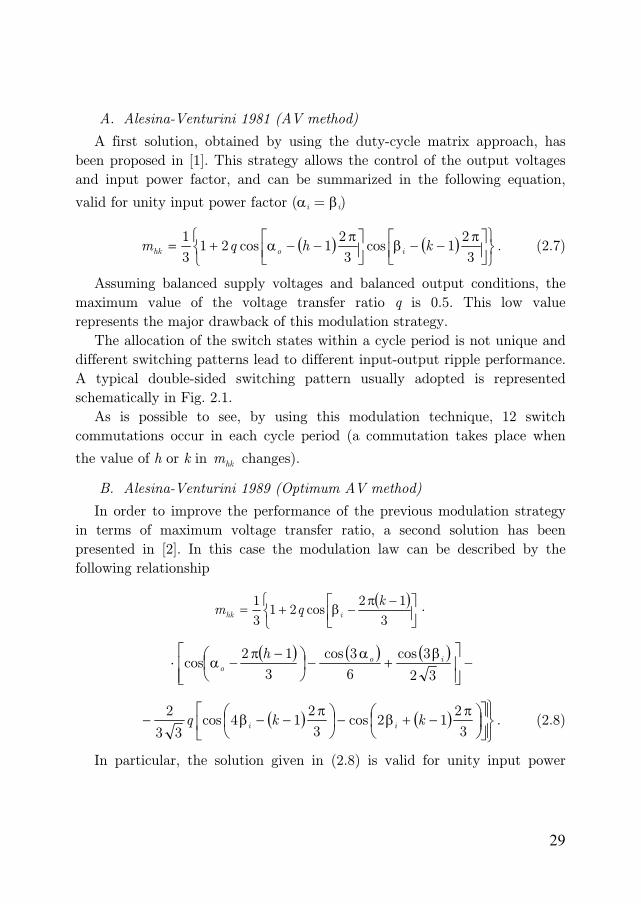
The position of any segment connecting the three duty-cycle space vectors
iβ
1m2m
3m
0m
Fig. 2.6(a) – Geometrical representation of the segment connecting 1m , 2m and 3m .
iβ
1m
2m3m
a)
c)
d)
b)
Fig. 2.6(b) – Geometrical representation of four typical positions of the segment connecting 1m , 2m and 3m .

43
can be arbitrarily changed by means of om , with the constraint that it has to
remain completely within the triangular region. The choice of om provides
two degrees of freedom, affecting the modulation features in terms of
maximum voltage transfer ratio, number of switch commutations and ripple
of the input/output quantities.
For given values of oα , iβ and iϕ , the maximum achievable value for the
voltage transfer ratio depends on how long can be the segment without
crossing the triangle boundary. The maximum length depends on the position
of the segment within the triangle and, as a consequence, from the selected
value of om .
As already mentioned, the number of switch commutations in a cycle
period depends on the position of 1m , 2m and 3m with respect to the
triangle boundaries and vertexes, and then once again on om . Four different
typical positions may occur, which are represented in Fig. 2.6(b).
When the segment is completely within the triangle (case a)) the values of
the nine duty-cycles hkm are within the interval [0,1]. Then 12 switch
commutations occur in a cycle period. In the case b), 3m lies on the triangle
boundary. Then 031 =m and, as a consequence, the number of switch
commutations in the cycle period is reduced to 10, being the switch 31S
always off.
In the case c), 1m and 3m lie both on the boundaries of the triangle
leading to 013 =m and 031 =m , with only 8 switch commutations in the
cycle period.
The same number of switch commutations occur in case d) where 1m
coincides with a vertex of the triangle. In this condition 111 =m , 012 =m
and 013 =m , then the switches 12S and 13S are always off whereas the
switch 11S is always on. These concepts will be discussed with further details
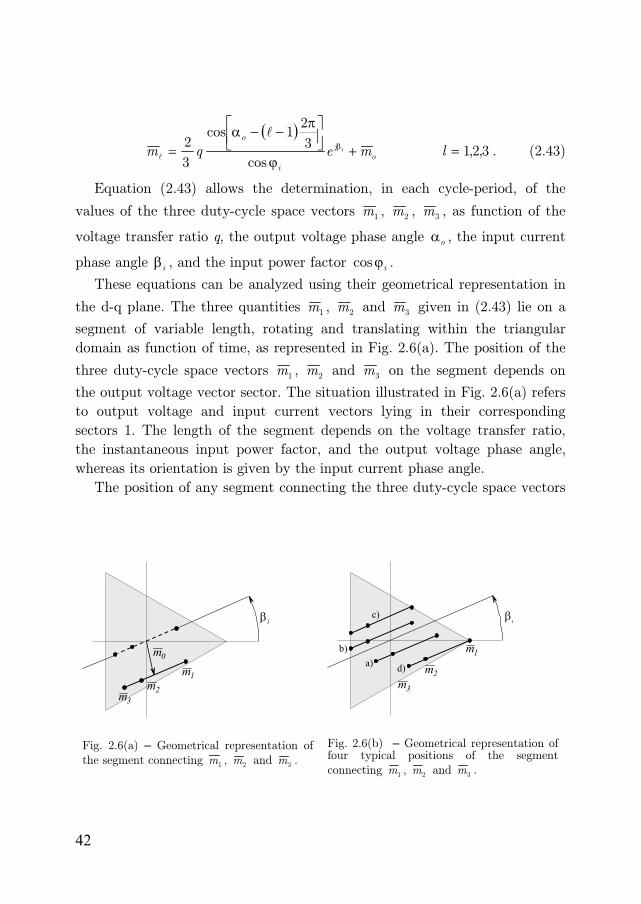
in Chapter 3.
At last, it is worthy to note that different values of om yield the same
average values for the input/output quantities in a cycle period, but they

44
determine different switching patterns and, as a consequence, different
performance in terms of ripple.
Substituting (2.43) in (2.26), leads to:
( ) ( )( )
3
21
cos
3
21cos
3
21cos
3
2
3
1π
−⋅+
ϕ
⎥⎦⎤
⎢⎣⎡ π
−−β⎥⎦⎤
⎢⎣⎡ π
−−α+=
kj
o
i
io
hk em
kl
qm (2.44)
where h=1,2,3 k=1,2,3.
This equation is a new and compact solution to the problem of
determining the modulation law for matrix converters. Equation (2.44) may
be considered also a direct generalization of the solution corresponding to the
AV method and the optimum AV method.
2.6. Comparison of the Modulation Strategies
Any modulation strategy can be represented using the DCSV approach
and analyzed from a new unitary point of view. In this way, a fair
comparison can be carried out in terms of voltage limits, number of switch
commutation, and ripple of the input/output quantities.
In order to do this it is sufficient to determine, for each modulation
technique, the expression of om , being dm and im prefixed by the reference
quantities, namely q, iϕcos , oα and iβ . Then, by using (2.43) it is possible
to evaluate the trajectories of the three duty-cycle space vectors 1m , 2m ,
3m , and the movement of the corresponding segment within the triangular
domain. In Fig. 2.7 some examples are shown with reference to operating
conditions characterized by input and output frequency of 50 Hz and 25 Hz
respectively, with a voltage transfer ratio of 0.5.
A. Alesina-Venturini 1981
Substituting (2.7) in (2.25), and then the obtained equation in (2.31),
leads to:
0=om . (2.45)
The movement of the segment connecting 1m , 2m and 3m is emphasized

45
in Fig. 2.7(a), whereas the trajectories of the three duty-cycle space vectors
are shown in Figs. 2.7(b), (c) and (d) respectively.
Fig. 2.7(a) shows six numbered segments, which have been obtained in six
successive time instants, equally spaced by 20 electrical degrees (with
reference to the input quantities). The ends of these segments draw the
trajectories of 1m and 3m , as shown in Figs. 2.7(b) and 2.7(d), respectively.
The numbered points in Figs. 2.7(b) – (d) refer to the corresponding segment
positions of Fig 2.7(a).
In this modulation strategy the two degrees of freedom related to the
choice of om are not utilized, then the segment substantially rotates around
the origin of the axis. In this way the performance in terms of maximum
voltage transfer ratio are very poor as emphasized in Fig. 2.11(a). In this
figure the surface representing the maximum voltage transfer ratio is shown
as function of the instantaneous values of oα and iβ , with unity input power
factor. Owing to the symmetry, the analysis has been restricted to values of
oα and iβ within the intervals [ ]oo 120,0 and [ ]oo 90,30− respectively.
The lower and the higher values are 0.5 and 1, respectively. The lower
value 0.5 determines the maximum voltage transfer ratio achievable in
balanced sinusoidal operating conditions, as also shown by the trajectories of
Fig. 2.7.
As far as the number of commutations are concerned, it can be noted
that the trajectories of 1m , 2m and 3m remain completely within the
1
3 4 5 6
2
a)
...
. ..6 54
32
1
b)
.... .. 65
4321
c)
..... .6
5
3
2
4
1
d)
Fig. 2.7 – Segment position a), trajectory of 1m b), 2m c) and 3m d) obtained by using AV
strategy with: ,5.0=q Hzf 501 = , Hzf 252 = .

46
boundary of the triangular region, without touching the triangle sides. As a
consequence, using this modulation technique, 12 switch commutations occur
in each cycle period.
It should be noted that the AV method does not provide any degree of
freedom, then the performance in terms of ripple of the input/output
quantities is intrinsically prefixed.
B. Alesina-Venturini 1989
Substituting (2.8) in (2.25) and then, the equation so obtained in (2.31),
leads to:
( ) ⎥⎦
⎤⎢⎣
⎡+−+−= β−βα−αβ iiooi jjjjj eeeee
qm 2433
03
7
3
1
18. (2.46)
As is possible to see, the presence of the zero component 0m of the duty-
cycle space vectors determines a rotation and a translation of the segment in
the d-q plane. This movement is emphasized in Fig. 2.8(a), whereas the
trajectories of the three duty-cycle space vectors 1m , 2m and 3m , are shown
in Figs. 2.8(b), (c) and (d), respectively. The maximum voltage transfer ratio
can be sensibly improved owing to this particular choice of om , as shown in
Fig. 2.11(b). The lower and the higher values are 0.866 and 0.945
respectively. The increase of the lower value to 0.866 has to be considered a
great advantage of this optimum AV method with reference to the basic AV
method, despite of a small reduction of the higher value.
Also in this case, the trajectories of 1m , 2m and 3m remain completely
1
2
3
45
6
a)
... . . .1-2-3
6
45
b)
. ... ..2
34
5
61
c)....
..4-5-6
3
2
1
d)
Fig. 2.8 – Segment position a), trajectory of 1m b), 2m c) and 3m d) obtained by using
optimum AV strategy with: ,5.0=q Hzf 501 = , Hzf 252 = .
47
within the boundary of the triangular region, without touching the triangle
sides, leading to 12 switch commutations in each cycle period.
Furthermore, as in AV method, the optimum AV method does not
provide any degree of freedom, then the performance in terms of ripple of the
input/output quantities is intrinsically prefixed.
C. SVM Technique
In order to achieve the expression of om for the SVM technique, reference
is made to Tab. 2.1, Tab. 2.2 and (2.14)-(2.17). In the case of output voltage
vector and input current vector both lying in their corresponding sectors 1,
after some manipulations, it is possible to obtain the following equation
( ) ( ) +⎥⎦
⎤⎢⎣
⎡α+β−α−β
ϕ=
ππ−
330
˜˜sin˜˜sincos33
2 j
oi
j
oi
i
eeq
m
⎟⎟⎠
⎞⎜⎜⎝
⎛δ+δ+δ+
ππ3
4
033
2
02013
2 jj
ee . (2.47)
Owing to the presence of the last term in (2.47), the value of 0m depends
on the particular selection of the zero configuration duty-cycles, leading to
two degrees of freedom.
With simple considerations it is possible to demonstrate that these degrees
of freedom correspond to the two degrees of freedom of the segment
represented in Fig. 2.6(a), which can translate anywhere within the
triangular region.
As a consequence, the SVM technique should not be considered a
particular modulation strategy, but indeed a synthesis of all the possible
modulation strategies. In fact, the AV and the optimum AV techniques can
be derived by the SVM technique with an opportune choice of 01δ , 02δ and
03δ , in each cycle period.
The movement of the segment related to SSVM technique is illustrated in
Fig. 2.9(a), whereas the trajectories of the three duty-cycle space vectors 1m ,
2m and 3m are shown in Figs. 2.9(b), (c) and (d), respectively. As is possible
to see, comparing Figs. 2.8 and Figs. 2.9, the behaviour of the SSVM
technique is quite similar to the behaviour of the optimum AV method. The

48
segment moves, without discontinuity, completely within the triangular
region, leading to 12 switch commutations in each cycle period.
The movement of the segment obtained using the ASVM technique is
illustrated in Fig. 2.10(a), whereas the trajectories of the three corresponding
duty-cycle space vectors 1m , 2m and 3m are shown in Figs. 2.10(b), (c) and
(d), respectively. This kind of movement is quite different from that obtained
using SSVM. The segment rotates around one of its ends, cantered on a
vertex of the triangle, which is determined by the actual sector of the input
current vector. Then, the position of the segment instantaneously changes as
the input current vector crosses the sector boundary. In this way, 8 switch
commutations occur in each cycle period.
With regard to the voltage transfer ratio, it is easy to demonstrate, with
geometrical consideration, that the maximum voltage transfer ratio
achievable with optimal positioning of the segment within the triangular
region equals the maximum voltage transfer ratio of the SVM technique
1
2
3
65
4
a)
. .....
65
4
1-2-3
b)
. ...
..6
5
432
1
c)
...
..
.
1
2
3
4-5-6
d)
Fig. 2.9 – Segment position a), trajectory of 1m b), 2m c) and 3m d) obtained by using
SSVM strategy with: ,5.0=q Hzf 501 = , Hzf 252 = .
3
65
4
2
1
a)
. . ..1-2-3
6 54
b)
.. ..
..6
5
4
3
2
1
c)
.
. .
.
1
2
3
4-5-6d)
Fig. 2.10 – Segment position a), trajectory of 1m b), 2m c) and 3m d) obtained by using
ASVM strategy with: ,5.0=q Hzf 501 = , Hzf 252 = .
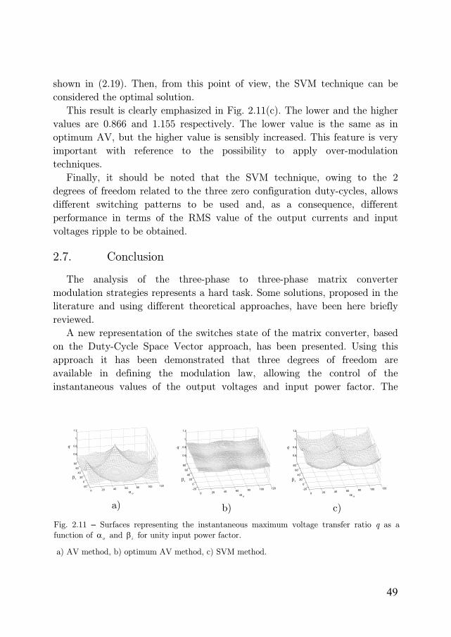
49
shown in (2.19). Then, from this point of view, the SVM technique can be
considered the optimal solution.
This result is clearly emphasized in Fig. 2.11(c). The lower and the higher
values are 0.866 and 1.155 respectively. The lower value is the same as in
optimum AV, but the higher value is sensibly increased. This feature is very
important with reference to the possibility to apply over-modulation
techniques.
Finally, it should be noted that the SVM technique, owing to the 2
degrees of freedom related to the three zero configuration duty-cycles, allows
different switching patterns to be used and, as a consequence, different
performance in terms of the RMS value of the output currents and input
voltages ripple to be obtained.
2.7. Conclusion
The analysis of the three-phase to three-phase matrix converter
modulation strategies represents a hard task. Some solutions, proposed in the
literature and using different theoretical approaches, have been here briefly
reviewed.
A new representation of the switches state of the matrix converter, based
on the Duty-Cycle Space Vector approach, has been presented. Using this
approach it has been demonstrated that three degrees of freedom are
available in defining the modulation law, allowing the control of the
instantaneous values of the output voltages and input power factor. The
0 20 40 60 80 100 120-20
0
20
40
60
80
0.6
0.8
1
1.2
oα
iβ
q
a)
0 20 40 60 80 100 120-20
0
20
40
60
80
0.6
0.8
1
1.2
oα
iβ
q
b)
0 20 40 60 80 100 120 -20
0
20
40
60
80
0.6
0.8
1
1.2
oα
iβ
q
c)
Fig. 2.11 – Surfaces representing the instantaneous maximum voltage transfer ratio q as a function of oα and iβ for unity input power factor.
a) AV method, b) optimum AV method, c) SVM method.

50
degrees of freedom reduce to only two if no information about the output
currents is used.
A compact and general solution to modulation problem of the matrix
converter, which includes the already-established modulation strategies as
particular cases, has been derived.
A useful geometrical representation of the duty-cycle space vector has
been presented. It provides a unitary point of view and simplifies the
comparison between different modulation strategies in terms of maximum
voltage transfer ratio, switching frequency and ripple of the input/output
quantities.
Owing to its intrinsic two degrees of freedom, SVM technique represents
the general solution of the matrix converter modulation problem, and can be
considered the best solution for the possibility to achieve the highest voltage
transfer ratio and to optimize the switching pattern through a suitable use of
the zero configurations.

51
3.Chapter 3 Advanced Modulation Strategies Abstract
The performance of matrix converters is strictly related to the modulation
strategy adopted to control the state of the switches. In the first part of this
chapter a novel modulation strategy, based on the measurement of the output
currents, is presented and discussed. The proposed strategy allows obtaining
sinusoidal input and output currents, like the well-known Space Vector
Modulation or Alesina-Venturini Modulation. However, compared to those
modulation strategies, it requires a lower number of switch commutations for
cycle period, thus leading to a sensible reduction of the converter switching
losses and of the effects related to the switching dead time. Furthermore, the
maximum voltage transfer ratio can be preserved.
In the second part of the chapter an analytical approach to predict the
current ripple in an inductive load fed by a matrix converter controlled with
Space Vector Modulation is presented. The analysis aims at determining the

52
optimal modulation strategy that minimizes the rms value of the load current
ripple. The minimization procedure is based on the analysis of the locus
described by the current ripple in the d-q reference frame. As a result, a set
of equations which allows the on-line calculation of the optimal SVM
switching pattern is found. It has been verified that it is possible to obtain a
current ripple lower than that of traditional SVM strategies, and with a
reduced number of commutations. Experimental results are provided to
confirm the theoretical approach.
3.1. Introduction
While the main features of the modulation theory for VSI are well-
established, the research on the modulation strategies for matrix converters
are still in progress.
Several solutions have been presented in Chapter 2. Each of them shows
different features in terms of number of switch commutations in a cycle
period and utilization of the input voltage.
To discuss this issue, it is convenient to introduce the concept of Branch
Switch Overs (BSOs). The number of BSO of a branch is defined as the
number of its state changes in a cycle period.
The voltage transfer ratio of Alesina and Venturini’s original theory, by
means of third harmonic injection techniques, can be increased up to 0.866, a
value which represents an intrinsic limitation of three-phase matrix
converters with balanced supply voltages [1].
The Optimum Alesina-Venturini method requires 12 BSOs per cycle
period [2].
The Scalar Control Algorithm proposed in [31], based on a different
approach, leads to similar performance.
In [34] a double-sided SVM strategy with 9 BSOs was proposed. Later, in
[35], it was shown that a proper selection of the switch sequence could reduce
the number of BSOs from 9 to 8 without deteriorating the performance of the
modulation strategy. Finally, in [36] a modified SVM strategy was proposed
in order to reduce the switch losses. This strategy can be applied only for
voltage transfer ratio lower than 0.5.
A comparison between different types of modulation strategies can be

53
found in [7], [37]-[39], showing that the ”indirect approach” for matrix
converter, initially preferred for its simplicity, is now partially replaced by
modern direct theories, that allow an immediate understanding of the
modulation process, without the need of a fictitious DC link.
The general and complete direct solution of the control problem of matrix
converters, described in Chapter 2, was originally presented in [7]. This
solution is based on the Duty-Cycle Space Vector (DCSV) approach, which
consists in the representation of the switch states by means of space vectors.
This approach has the advantage to emphasize all the parameters
affecting the performance of the modulation strategy, such as the common
mode voltage and the output currents.
It should be noted that the modulation techniques cited above do not
utilise any information about the output currents. The main reason is that,
at a first glance, a modulation strategy avoiding the use of current sensors, is
desirable.
However, in several applications involving electric motor drives, the load
currents must be monitored and directly controlled. In these cases, the
current sensors are required without regard to the type of converter feeding
the motor, and the current measurement can be used also for improving the
performance of the modulation strategy.
Exploiting the features of the DCSV approach, a novel modulation
strategy based on the measurement of the output currents is proposed and
analysed in the first part of this chapter. Compared with the well-established
strategies, its main advantage is the reduction of the number of BSOs in a
cycle period from 8 to 6, thus decreasing the switch losses and the effects of
the switch dead time [40],[41].
Furthermore, this advantage is obtained without deteriorating the quality
of the input/output voltages and currents and preserving the maximum
voltage transfer ratio.
3.2. Duty-Cycle Space Vector Approach
The matrix converter input-output relationships can be easily expressed
introducing the concept of ”Duty-Cycle Space Vector” exposed in Chapter 2.
According to this principle, the duty-cycles 11m , 12m and 13m of the three

54
switches S11, S12, S13 of the first branch of the converter shown in Fig. 1.1 can
be represented by the space vector 1m given by (2.1).
The geometrical representation of 1m in the d-q plane shows that all the
acceptable values for 1m are inside the region represented in Fig. 3.1 by the
equilateral triangle ABC. It can be noted that the distances between 1m and
the triangle sides directly represent the values of the duty-cycles m11, m12 and
m13.
The position of the space vector 1m inside the triangle determines the
number of switch commutations of 11S , 12S and 13S in a cycle period, and
consequently defines the number of BSOs of the first branch.
Furthermore, modern modulation strategies are usually ”double-sided” or
”symmetrical”, meaning that the turn-on sequence of the switches is
completed in the first half of the cycle period and it is repeated with inverse
order in the second half of the cycle period. In such a way, useless
commutations can be avoided, if the switch state at the beginning of the
current cycle period is equal to the switch state at the end of the previous
cycle period.
If 1m lies inside the triangle, all the duty-cycles are expected to be greater
than zero and the corresponding number of BSOs for a double-sided turn-on
sequence of the switches is 4. For instance, a possible symmetrical sequence
for the switches S11 , S12 and S13 concerning the first output phase could be
⎟⎠⎞
⎜⎝⎛= 0,3
2A
⎟⎠
⎞⎜⎝
⎛ −=3
1,
3
1B
⎟⎠
⎞⎜⎝
⎛−−=
3
1,
3
1C
M1
m13
m11m12
Fig. 3.1 – Graphical meaning of the duty-cycle space vector 1m .

55
S11→S12→S13→S12→S11, where each arrow corresponds to one BSO.
If 1m lies on a triangle side, then at least one duty-cycle among m11, m12,
m13 is zero. This means that the corresponding switch never turns on during
the cycle period and the number of BSOs reduces to 2.
Finally, if 1m is on a triangle vertex, two duty-cycles are zero. In this case
the number of BSOs is zero, because the state of the branch never changes
during the cycle period.
The same considerations can be carried out for the second and the third
branch of the converter in Fig. 1.1, introducing the duty-cycle space vectors
2m and 3m respectively. The number of BSOs can be derived in general
form as shown in Tab. 3.1.
3.3. Generalized Modulation Strategy
The problem of determining a modulation strategy is completely defined
by (2.39) and (2.40), here reported for convenience:
( ) **
,
3 oirefi
refrefo
divv
vm
λ+
ψ⋅ψ
= (2.39’)
( ) oirefi
refrefo
iivv
vm
*
*,
3
λ−
ψ⋅ψ
= (2.40’)
being the phase angle of refψ the desired phase angle for the input current
space vector and refov , the desired output voltage vector.
The parameter λ together with om yield three degrees of freedom, which
can be utilized in defining any type of modulation strategy.
After the calculation of dm and im by means of (2.39)-(2.40), (2.32)-(2.34)
TABLE 3.1 – NUMBER OF BSOS OF THE K-TH BRANCH FOR A DOUBLE-SIDED SWITCHING PATTERN.
Position of km (k=1,2,3) Number of BSOs
Inside the triangle 4 On a triangle side 2
On a triangle vertex 0

56
can be used to determine 1m , 2m and 3m . As is possible to see, the
parameter λ can be utilized as a degree of freedom only if the phase angle of
oi is known in each cycle period, otherwise it should be set to 0.
Finally, from 1m , 2m and 3m , one obtains the duty-cycles of the matrix
converter switches, which can be used as input commands for the converter,
by means of (2.26).
Taking (2.39) and (2.40) into account, (2.32) - (2.34) lead to:
( )( )
03
21
22
3
21
, 2
3
2mveji
ivj
v
evm i
kj
o
oi
ref
refi
kj
refo
k +⎥⎦
⎤⎢⎣
⎡⋅
λ+ψ
ψ⋅⋅
=π
−
π−
k=1,2,3. (3.1)
Equation (3.1) can be rewritten in a more compact form as follows:
okkk mBAm +λ+= (3.2)
where
( )
ref
refi
kj
refok
v
evA ψ
ψ⋅⋅
=
π−
3
21
,
3
2 (3.3)
( )
i
kj
o
oi
k vejiiv
jB ⎥⎦
⎤⎢⎣
⎡⋅=
π−
3
21
22
2. (3.4)
As can be seen in (3.3) - (3.4), kA and kB can be calculated using
reference and measured quantities.
Equation (3.1), which allows the determination of the values of the three
duty-cycle space vectors 1m , 2m , 3m in each cycle-period, can be analyzed
using a geometrical representation in the d-q plane.
Assuming λ = 0, a value implicitly adopted for defining the modulation
laws in [1]–[6], [34]-[39] the three quantities 1m , 2m and 3m lie on a line
segment. The segment length depends on the voltage transfer ratio, the
instantaneous input power factor, and the output voltage phase angle,
whereas its orientation is given by the input current phase angle.
The line segment can be arbitrarily moved within the triangle by varying

57
om . This provides two degrees of freedom, affecting the maximum voltage
transfer ratio, the total number of BSOs in a cycle period and the ripple of
the input/output quantities. Four typical positions can be defined for the
segment, already shown in Fig. 2.6(b):
a) the line segment is completely inside the triangle. In this case the total
number of BSOs is 12 (4 BSOs for each branch);
b) one end point of the line segment lies on a triangle side. In this case the
total number of BSOs is 10 (2 BSOs for one branch and 4 BSOs for the
others);
c) both the end points of the line segment lie on triangle sides. The total
number of BSOs is 8 (two branches present 2 BSOs and the other one
presents 4 BSOs);
d) one end point of the line segment coincides with a triangle vertex. The
total number of BSOs is 8 (one branch does not present any BSO, each one
of the others presents 4 BSOs).
These results are summarised in Tab. 3.2.
It is important to note that the already-known modulation strategies can
be reviewed according to the DCSV approach. For instance, Optimal Alesina-
Venturini Modulation Strategy and the particular type of SVM that uses 3
zero vectors belong to case a) and present 12 BSOs.
The SVM that uses 2 zero vectors belongs to case b) and presents 10
BSOs. The SVM that uses 1 zero vector belongs to case c) or d) and presents
8 BSOs.
3.4. Modulation Strategy with Minimum BSOs
In this paragraph, a novel approach, that makes use of the parameter λ in
order to reduce the total number of BSOs in a cycle period, is discussed. As
TABLE 3.2 TOTAL NUMBER OF BSOS FOR DOUBLE-SIDED SWITCHING
PATTERN WITH REFERENCE TO FIG. 3.1
Case Total number of BSOs a) 12 b) 10 c) 8 d) 8

58
is possible to see from (2.39) and (2.40), if the phase angle of oi is known in
each cycle period, the parameter λ can be utilized as a further degree of
freedom. In particular, as is possible to see from (3.1), the parameter λ moves
1m , 2m and 3m along straight lines that are perpendicular to the input
voltage space vector. It will be shown that, with an opportune selection of
the value of the parameters λ and 0m , it is always possible to move one
duty-cycle space vector to a triangle vertex and at least another one to a
triangle side.
Thus the total number of BSOs in a cycle period is reduced to only 6. In
this way a significant reduction of the switching frequency with respect to
the already-known modulation strategies is achieved.
Here, the basic principle of the modulation strategy is summarised with
reference to the example shown in Fig. 3.2.
The value of om can be selected in order to move the segment so that one
of its ends coincides with one vertex of the triangle, defined on the basis of
the input current direction. In this way one of the duty-cycles space vector
( 1m in the example) is fully determined, because its position is known.
Starting from an initial null value of λ and varying the value of this
parameter, 2m and 3m migrate from their initial positions along two straight
lines (r and s). By an appropriate selection of om , it is possible to keep the
1m
2m
3m
d
q
r
s
Fig.3.2 – Example of migration of 1m , 2m and 3m due to a non-null value of λ.

59
position of 1m unchanged for any value of λ. Thus the values of λ bringing
2m or 3m on a triangle side can be found. From a geometrical point of view,
this can be done finding the six values of λ corresponding to the intersections
between the straight lines r and s, expressed in a parametric form, with the
straight lines to which the triangle sides belong.
Among these six values, let λp be the minimum among the positive
values and λn the maximum among the negative ones. It is worth noting that
values of λ external to the interval [λn, λp] lead 2m or 3m out of the triangle,
which represents the validity domain.
To reduce the number of BSOs, λ can assume indifferently the values λn
or λp. Once the values of λ and om are defined, it is possible to determine 2m
and 3m , thus giving the complete solution of the modulation problem with
only 6 BSOs.
The algorithm for the selection of λ and om in the general case is
presented in Appendix A.
3.5. Simulation Results
To verify the analytical approach, the behaviour of the proposed
modulation strategy has been tested with numerical simulation for a system
composed by a non-ideal supply, an input L-C filter and a matrix converter
feeding a three-phase symmetrical R-L passive load. The basic scheme of the
system is shown in Fig. 3.3 and the values of the system parameters are
reported in Tab. 3.3.
The behaviour of the proposed modulation strategy has been also
compared with some well-established modulation strategies based on SVM.
Figs. 3.4, 3.5 and 3.6 represent the waveform of the input voltage (a), the
line current (b) and the output current (c) for three different modulation
strategies, namely the SVM that uses one zero vector placed at the beginning
of the cycle period (8 BSOs), the SVM that uses two zero vectors placed at
the beginning and in the middle of the switching period (10 BSOs), and the
new modulation strategy (6 BSOs). The simulations have been carried out for

60
a cycle period Tp of 200 μs, that is generally sufficient for the implementation
of the control algorithm.
As can be seen, the new modulation strategy determines practically the
same current and voltage ripple as the SVM with one zero vector, while the
SVM with two zero vectors performs better than the other modulation
techniques.
To make a fair comparison, the cycle period should be changed in order to
cause the same BSOs per second for each modulation strategy. As a
consequence, a cycle period of 250 μs has been assumed for the SVM with
two zero vectors, while a cycle period of 150 μs has been used for the new
modulation strategy. The behaviour of these modulation strategies is shown
in Fig. 3.7 and 3.8 respectively. The cycle period for the SVM with one zero
vector has been kept unchanged.
As can be seen, although the new modulation has only 6 BSOs, its
performance is comparable with the SVM with 10 BSOs, and is better than
the SVM with 8 BSOs.
ii
Matrix inverter
Rs Ls RL LL
Non ideal voltage supply Input filter Load
ivsv
ii
Digital controller
id mm ,Lf
Cfov oi
Fig. 3.3 - Basic matrix converter scheme using the space vector notation.
TABLE 3.3SYSTEM PARAMETERS
Supply VS(rms) = 220 V, ωS = 2π 50 rad/s, RS = 0.25 Ω, LS=0.4 mH
Filter Lf = 0.6 mH, Cf = 10.0 μF
Load Rl = 10 Ω, Ll = 20 mH, ωo = 2π 25 rad/s

61
Furthermore, the reduction of the number of BSOs allows to limit the
effects related to the switch dead-time.
3.6. Preliminary Conclusion
A new modulation strategy for matrix converters, based on the output
current sensing and characterized by only 6 BSOs for cycle period, has been
presented. The reduced number of BSOs leads to a sensible reduction of the
converter switching losses and of the effects related to the switch dead time,
without deteriorating the quality of the input/output voltages and currents.
The modulation strategy has been developed using the Duty-Cycle Space
-400
-200
0
200
400
Time (2 ms / div)
Inpu
t vol
tage
(V)
(a)
-10
-5
0
5
10
Time (2 ms / div)
Line
cur
rent
(A)
(b)
-20
-10
0
10
20
Time (2 ms / div)
Out
put c
urre
nt (A
)
(c)
Fig. 3.4 - SVM with one zero vector placed at the beginning of the cycle period (8 BSOs). Cycle period of 200 μs. (a) input voltage, (b) line current, (c) output current.

62
Vector Theory, which allows, through a simple and direct geometrical
representation, an immediate comprehension of the modulation basic
principles.
The performance of the new modulation strategy and of the well-known
SVM, in terms of ripple of input and output quantities, has been analyzed by
means of realistic numerical simulations. The comparison has been carried
out assuming either the same cycle period or the same switching frequency.
The obtained results clearly emphasize the effectiveness of the proposed
modulation strategy.
-4 0 0
-2 0 0
0
2 0 0
4 0 0
T im e (2 m s / d iv )
Inpu
t vol
tage
(V)
(a)
-10
-5
0
5
10
Time (2 ms / div)
Line
cur
rent
(A)
(b)
-20
-10
0
10
20
Time (2 ms / div)
Out
put c
urre
nt (A
)
(c)
Fig. 3.5 - SVM with two zero vectors placed at the beginning and at the middle of the cycleperiod (10 BSOs). Cycle period of 200 μs. (a) Input voltage, (b) line current, (c) outputcurrent.
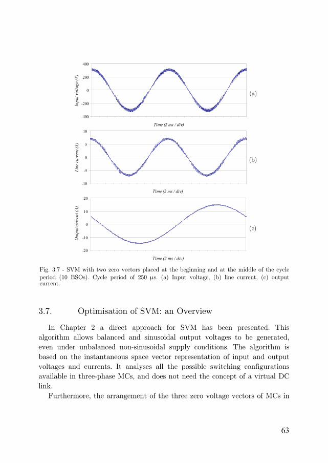
63
3.7. Optimisation of SVM: an Overview
In Chapter 2 a direct approach for SVM has been presented. This
algorithm allows balanced and sinusoidal output voltages to be generated,
even under unbalanced non-sinusoidal supply conditions. The algorithm is
based on the instantaneous space vector representation of input and output
voltages and currents. It analyses all the possible switching configurations
available in three-phase MCs, and does not need the concept of a virtual DC
link.
Furthermore, the arrangement of the three zero voltage vectors of MCs in
-400
-200
0
200
400
Time (2 ms / div)
Inpu
t vol
tage
(V)
(a)
-10
-5
0
5
10
Time (2 ms / div)
Line
cur
rent
(A)
(b)
-20
-10
0
10
20
Time (2 ms / div)
Out
put c
urre
nt (A
)
(c)
Fig. 3.7 - SVM with two zero vectors placed at the beginning and at the middle of the cycle period (10 BSOs). Cycle period of 250 μs. (a) Input voltage, (b) line current, (c) output current.

64
the switching pattern offers some degrees of freedom that the designer can
usefully utilize to improve the modulation strategy.
The remaining paragraphs of this chapter will discuss the relationship
existing between the rms value of the current ripple and the arrangement of
the zero voltage vectors. In fact, a widely-used method to evaluate the
relative merits of different modulation techniques is to calculate the rms
value of the load current ripple, which is strongly related to torque ripple and
motor heating.
Finally a method for predicting the minimum rms value of the load
current ripple in each cycle period is presented. The result of the analysis
consists of very simple equations, which can be used in digital control
systems for the on-line implementation of the optimal modulation technique.
-400
-200
0
200
400
Time (2 ms / div)
Inpu
t vol
tage
(V)
(a)
-10
-5
0
5
10
Time (2 ms / div)
Line
curr
ent (
A)
(b)
-20
-10
0
10
20
Time (2 ms / div)
Out
put c
urre
nt (A
)
(c)
Fig. 3.6 - New modulation strategy (6 BSOs). Cycle period of 200 μs. (a) Input voltage, (b) line current, (c) output current.

65
This technique produces a current ripple lower than that of traditional
SVM strategies for MCs and, in operating conditions with high values of the
modulation index, it produces also a reduction of the number of
commutations.
3.8. SVM for MCs
A. Basic Principles
The SVM algorithm for MCs is able to synthesize the reference output
voltage vector refov , and to control the phase angle of the input current
vector selecting 4 non-zero configurations, applied for suitable time intervals
-400
-200
0
200
400
Time (2 ms / div)
Inpu
t vol
tage
(V)
(a)
-10
-5
0
5
10
Time (2 ms / div)
Line
curr
ent (
A)
(b)
-20
-10
0
10
20
Time (2 ms / div)
Out
put c
urre
nt (A
)
(c)
Fig. 3.8 - New modulation strategy (6 BSOs). Cycle period of 150 μs. (a) Input voltage, (b) line current, (c) output current.

66
within the cycle period pT . The three zero configurations available in MCs
are applied to complete pT .
Therefore, the reference output voltage can be written as follows:
44332211, vvvvv refo δ+δ+δ+δ= (3.5)
where 1v , 2v , 3v and 4v are the output voltage vectors corresponding to the
4 selected configurations, and δ1, δ2, δ3 and δ4 are the duty-cycles, defined as
p
kk
T
T=δ , k=1,2,3,4. (3.6)
In (3.6), T1, T2, T3 and T4 are the time intervals of application of 1v , 2v ,
3v and 4v .
Once δ1 , δ2 , δ3 and δ4 are found, it is necessary to define the switching
pattern, namely the turn-on and turn-off sequence of the switches.
B. Degrees of freedom in the switching patterns
It is a general principle that, once the reference output voltage vector and
the input current displacement angle are given, the SVM univocally
determines the switching pattern. In fact, among all possible switching
sequences involving 1v , 2v , 3v , 4v and the three zero vectors, there is only
one commutation sequence characterized by only one switch commutation for
each switching configuration change.
The SVM algorithm can be simplified to some extent taking advantage of
its symmetries if the d-q plane is divided into 6 sectors for the output voltage
vectors and the input current vectors as shown in Figs. 2.2(a)-(b). Hence, in
the following, the input voltage vector and the reference output voltage
vector are assumed in sector 1. In addition it is assumed that the goal of the
control system is to keep the input current in phase with the input voltage
vector, leading to unity input power factor.
Fig. 3.9 shows the switching sequence corresponding to the case of Fig.
2.2(a)-(b). As can be seen, the use of the three zero configurations leads to 12
switch commutations in each cycle period. It should be noted that the
possibility to select the duty-cycles of three zero configurations gives only two

67
degrees of freedom, being
4321030201 1 δ−δ−δ−δ−=δ+δ+δ (3.7)
where δ01, δ02 and δ03 are the duty-cycles of the 3 zero voltage vectors )1(0v ,
)2(0v and )3(0v . These two degrees of freedom will be used to define different
switching patterns, characterized by different behaviour in terms of ripple of
the input and output quantities. The two degrees of freedom might be
utilized also to eliminate one or two zero configurations, affecting also the
number of commutations in each cycle period.
In the following, the switching frequency sf is defined as the total number
of BSOs per second.
The traditional SVM strategies considered in this chapter and their
switching frequencies are reported in Tab. 3.4.
Strategies 1-3 are characterized by only one zero configuration for each
half of the switching pattern. Using these strategies the number of switch
commutations in each cycle period is 8. A particular case is Strategy 1, which
uses only the zero configuration located in the middle of each half of the
switching pattern (vector )1(0v in Fig. 3.9). In this way, the switches of one
column (in this case the first one of Fig. 1.1) of the MC do not change their
state ( 11S is always on, 12S and 13S are always off in Fig. 3.3).
Strategies 4–6 use two zero configurations, determining 10 commutations
in a cycle period.
Finally, Strategy 7 is characterized by the fact that all zero configurations
are used with equal duty-cycles. As a consequence, 12 switch commutations
S11S13 S12
S23 S21
S31
S22
S32S33
0321 T 022
1 T0121 T12
1 T 221 T 32
1 T 421 T
4v3v1v 2v )1(0v)3(0v )2(0v
pT21
0321 T
0221 T 012
1 T 121 T22
1 T321 T42
1 T
4v 3v 1v2v)1(0v)3(0v)2(0v
pT21
S12
S22
S32
S11
S21
S31
S13
S33
S23
Fig. 3.9 – Double-sided switching pattern in a cycle period Tp, with reference to the case shown in Fig. 2.

68
occur in each cycle period.
3.9. Analysis of the Load Current Ripple
If the reference voltage vector refov , could be ideally applied to the load,
the corresponding current would be refoi , . However, the actual value of the
output voltage ov differs from refov , because ov can assume only a finite
number of values. Hence, it is possible to define the output voltage and
current ripple vectors as follows
refoorip vvv ,−= (3.8)
refoorip iii ,−= (3.9)
where oi is the actual value of the load current vector, and refoi , is its mean
value over the cycle period. According to the principles of the SVM
technique, the mean value of ripv during a cycle period Tp is zero.
For an inductive load, the high frequency relationship between ripv and
ripi can be written as follows
L
riprip
L
v
dt
id= (3.10)
TABLE 3.4 – STRATEGIES FOR SVM
Strategy number Defining equation Switching frequency
1 00302 =δ=δ fs=8/Tp
2 00301 =δ=δ fs=8/Tp
3 00201 =δ=δ fs=8/Tp
4 (Asymmetrical) 0, 010302 =δδ=δ fs=10/Tp
5 0, 020301 =δδ=δ fs=10/Tp
6 0, 030201 =δδ=δ fs=10/Tp
7 (Symmetrical) 030201 δ=δ=δ fs=12/Tp

69
where LL is the load inductance.
Also the current ripple has zero mean value in a cycle period. Taking (3.6)
into account, it is possible to determine the locus described in the stationary
d-q reference frame by the vector ripi during Tp. Fig. 3.10 shows the locus
obtained with reference to the switching pattern of Fig. 3.9.
At the beginning of the cycle period, ripi is zero, corresponding to the
point O, origin of the reference frame. After a time interval T03/2 , during
which the zero vector )3(0v is applied to the load, ripi reaches point A and the
current ripple vector changes by the quantity AO given by
refo
L
p vL
TAO ,
03
2
δ−= . (3.11)
During the second interval of length 121 T , the vector 1v is applied to the
load and ripi changes by the quantity BA given by
( )refo
L
p vvL
TBA ,1
1
2−
δ= , (3.12)
thus reaching the point B. The ripple vector ripi reaches the points C, D, E
and F in sequence (corresponding to the application of the vectors 2v , )1(0v ,
3v and 4v shown in Fig. 3.9). After the application of the vector )2(0v , ripi
A
B
C
D
E
F
O
F’
E’
D’
C’
B’
A’
d
q refov ,
Fig. 3.10 – Locus described by the current ripple vector in the d-q plane.

70
reaches the point O again in the middle of the cycle period. Afterwards, ripi
symmetrically covers the second half of the locus passing through F’, E’, D’
C’, B’, A’ and finally returns to O.
It is worth noting that the length of the segments AO, DC and OF is
proportional to δ01, δ02 and δ03 respectively. Therefore, the shape of the locus
depends on the splitting of the total time δ0. For example, Fig. 3.11 shows
the locus of the load current ripple for the same case of Fig. 3.10, but with δ02
= 0 (C coincides with D). As can be seen, it is rather different from the one
shown in Fig. 3.10, and the overall ripple is likely greater.
3.10. Optimal Space Vector Modulation Strategy
The parameter that is commonly used to represent the distortion of the
current waveform is the rms value of its ripple, defined as
2,,3
2,,2
2,,1, rmsripormsripormsripormsrip iiiI ++= . (3.13)
where io1,rip,rms, io2,rip,rms and io3,rip,rms are the rms values of the ripple of the three
load currents.
As the locus described by ripi is symmetrical with respect to the origin of
the reference frame, the rms value of the current ripple, in terms of the space
vector ripi , can be written as follows:
A
B
C=D
E
F
O
F’
E’
C’=D
B’
A’
Fig. 3.11 – Locus described by the current ripple vector in the d-q plane for the case δ02 = 0.
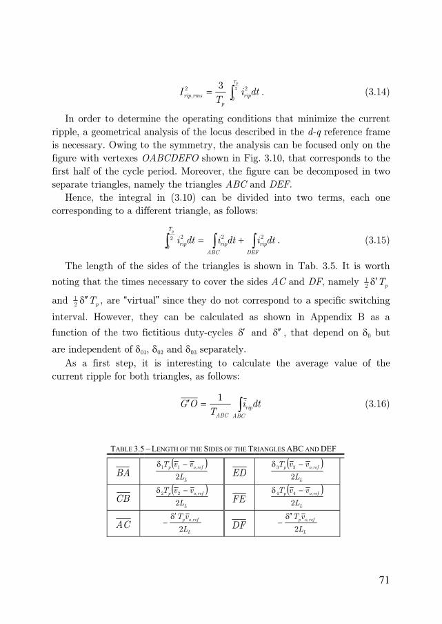
71
∫= 2
0
22,
3 pT
dtiT
I rip
p
rmsrip . (3.14)
In order to determine the operating conditions that minimize the current
ripple, a geometrical analysis of the locus described in the d-q reference frame
is necessary. Owing to the symmetry, the analysis can be focused only on the
figure with vertexes OABCDEFO shown in Fig. 3.10, that corresponds to the
first half of the cycle period. Moreover, the figure can be decomposed in two
separate triangles, namely the triangles ABC and DEF.
Hence, the integral in (3.10) can be divided into two terms, each one
corresponding to a different triangle, as follows:
∫∫∫ +=DEF
rip
ABC
rip
T
rip dtidtidtip
222
0
2 . (3.15)
The length of the sides of the triangles is shown in Tab. 3.5. It is worth
noting that the times necessary to cover the sides AC and DF, namely pTδ′21
and pTδ ′′21 , are “virtual” since they do not correspond to a specific switching
interval. However, they can be calculated as shown in Appendix B as a
function of the two fictitious duty-cycles δ′ and δ ′′ , that depend on δ0 but
are independent of δ01, δ02 and δ03 separately.
As a first step, it is interesting to calculate the average value of the
current ripple for both triangles, as follows:
∫=′ABC
rip
ABC
dtiT
OG1
(3.16)
TABLE 3.5 – LENGTH OF THE SIDES OF THE TRIANGLES ABC AND DEF
BA ( )
L
refop
L
vvT
2
,11 −δ ED
( )L
refop
L
vvT
2
,33 −δ
CB ( )
L
refop
L
vvT
2
,22 −δ FE
( )L
refop
L
vvT
2
,44 −δ
AC L
refop
L
vT
2
,δ′− DF
L
refop
L
vT
2
,δ ′′−

72
∫=′′DEF
rip
DEF
dtiT
OG1
(3.17)
where TABC and TDEF are the total times required to cover the triangles ABC
ed DEF, defined as
( )δ′+δ+δ= 2121
pABC TT (3.18)
( )δ ′′+δ+δ= 4321
pDEF TT . (3.19)
It is worth noting that TABC and TDEF are independent of the duty-cycles
δ01, δ02 and δ03 as well. Obviously, their sum is equal to half the cycle period,
i.e.
pDEFABC TTT 21=+ . (3.20)
It can be verified that (3.16) and (3.17) are similar to the equations used
to calculate the centre of gravity of a mechanical system with respect to the
point O, origin of the reference frame. Like in mechanics, the positions of the
points G′ and G ′′ are independent from the point O. Hence, it is convenient
to refer ripi to G′ and G ′′ . For the triangle ABC, the current ripple ripi can
be written introducing the new space vector i ′ defined as follows:
OGiirip ′+= ’ . (3.21)
Since OG′ is the average value of ripi over ABC, the average value of i ′
over TABC is zero. Similarly, for the triangle DEF, the current ripple can be
expressed introducing the new space vector i ′′ , whose average value is zero in
the time interval TDEF, as follows:
OGiirip ′′+′′= . (3.22)
Substituting (3.21) and (3.22) in (3.14) leads to the following result:
∫∫∫ ′′+′+′′+′=DEFABC
DEF
T
ABCrip dtidtiOGTOGTdtip
2222
2
0
2 . (3.23)
The two integral terms in (3.23) are independent from the duty-cycles δ01,

73
δ02 and δ03. Therefore the rms value of the current ripple is minimum when
both vectors OG′ and OG ′′ have the minimum length. This condition is
achieved when the projections of G′ and G ′′ on the line AF coincide with the
point O, as shown in Fig. 3.12.
For the application of this basic principle it is useful to introduce the
parameters λ and μ defined as
ABCT
T03=λ (3.24)
DEFT
T02=μ . (3.25)
The geometrical condition shown in Fig. 3.12, after some analytical
developments, leads to the following optimal values for λ and μ:
( ) ( )( )⎥⎦
⎤⎢⎣
⎡δδ+δ+δδ
δ−δδδ+δ=λ
2122
21
2121
’42
1’sgnopt (3.26)
( ) ( )( )⎥⎦
⎤⎢⎣
⎡δδ+δ+δδ ′′
δ−δδδ+δ ′′=μ
3424
23
3443
42
1sgnopt . (3.27)
The mathematical procedure used to obtain (3.26) and (3.27) is similar to
that applied in [42] for traditional VSIs.
A
B
D
E
FO
C
G'
G''
Fig. 3.12 – Half of the locus described by the current ripple vector in the condition of minimum ripple.

74
The optimal values for δ03 and δ02 are
{ }0,03 0 δδ′λ=δ ˝,, max—min optopt (3.28)
{ }0,02 0 δδ ′′μ=δ ˝,, max—min optopt (3.29)
and δ01,opt is given by
δ01,opt = δ0 - δ02,opt - δ03,opt. (3.30)
Equations (3.28) and (3.29) ensure that δ03,opt and δ02,opt are positive and
lower than δ0. However, since δ02,opt and δ03,opt are found minimizing the two
distances OG′ and OG ′′ separately, it can happen that the condition
δ01,opt > 0 (3.31)
is not satisfied. In this case, it is necessary to assume
δ01,opt = 0 (3.32)
and (3.28) and (3.29) are replaced by the following equations:
( ){ +δ+δ+δ′δ′λ=δ 21,03 max—minopt
( )( ) }0,, - δδ′′μδδ+δ+δ′′+ 0034 (3.33)
δ02,opt = δ0 - δ03,opt . (3.34)
3.11. Simulation Results
To characterize the behaviour of the modulation strategies, it is opportune
to introduce an appropriate quality index. This quality index could be the
mean value of the 2,rmsripI evaluated over the range [0,2π] of the phase angles
α and β of the output and input voltage vectors. The index is defined as
follows:
∫ ∫π π
βαβαππ
=2
0
2
0
2, ),(
2
1
2
1ddIQ rmsrip . (3.35)
Fig. 3.13 shows the behaviour of Q as a function of the modulation index

75
q, namely the ratio between the magnitudes of the output and the input
voltage vectors. Fig. 3.13 has been normalized with respect to the value of Q
for q = 2/3 using the optimal modulation strategy. It can be noted that
the behaviour of the optimal strategy is better than that of the other
strategies for any value of q. In addition, the optimal modulation is superior
to Strategy 7 in terms of mean switching frequency, for high values of q. In
fact, in these operating conditions the optimal strategy tends to perform like
Strategy 4. This is confirmed in Fig. 3.14, where the switching frequency,
expressed in p.u. of the switching frequency of Strategy 7 is plotted as
function of q for the different types of modulation strategies.
3.12. Experimental Results
In order to verify the theoretical approach, a prototype of a three-phase to
three-phase MC has been used to supply a linear passive R-L load. The MC
is realized using the FM35E12KR3 IGBT module produced by EUPEC. The
control algorithm is implemented on the platform C6711, a floating-point
digital signal processor provided by Texas Instruments. The switching
frequency of the SVM strategies is 12.5 kHz, corresponding to a cycle period
0 0.1 0.2 0.3 0.4 0.5 0.6 0.7 0.80
0.5
1
1.5
2
2.5
3
3.5
Opt (7)
(2), (3)
(1) (5), (6)
(4)
Nor
mal
ized
val
ue o
f Q
Modulation index, q
Fig. 3.13 - Behavior of the quality index Q as a function of the modulation index q for Strategies (1)-(7) and for the optimal strategy (Opt). All curves are normalized with respect to
the value of Q for q = 2/3 using the optimal modulation strategy.

76
of 80 μs. The converter is fed by a voltage transformer with variable voltage
transfer ratio to adjust the input voltage to a value of about 110 V rms. A L-
C filter is connected at the input side of the converter. The parameters of
filter, supply and load correspond to those reported in Tab. 3.6.
Fig. 3.15 shows the behaviour of the traditional modulation strategies and
of the optimal strategy in terms of squared rms value of the load current
ripple. The rms value of the ripple has been determined by sampling the
current waveforms and considering only the high frequency harmonics. As
can be seen, the optimal modulation exhibits the lowest ripple, and the
behaviour of the curves is similar to that predicted in Fig. 3.13.
3.13. Conclusion
A geometrical approach for the analysis of the load current ripple in SVM
for MCs has been presented. The proposed method has been applied to define
0 0.1 0.2 0.3 0.4 0.5 0.6 0.7 0.80.5
0.55
0.6
0.65
0.7
0.75
0.8
0.85
0.9
0.95
1
Modulation index, q
Nor
mal
ized
switc
hing
freu
qncy
Opt
(7)
(1), (2), (3)
(4), (5), (6)
Fig. 3.14 - Behaviour of the switching frequency for all the modulation strategies in p.u. of theswitching frequency of Strategy 7.
TABLE 3.6
SYSTEM PARAMETERS.
Supply Filter Load
VS = 110 V(rms),
ωi = 2π 50 rad/s,
RS = 0.2 Ω, LS=0.70 mH
Lf = 1.16 mH
Cf = 4.5 μF
Rf = 300 Ω
RL = 8.3 Ω
LL = 1.3 mH,
ωo = 2π 100 rad/s

77
the optimal SVM technique, characterized by the minimum rms value of the
load current ripple in each cycle period and, as a consequence, over the
fundamental period. The explicit equations to calculate the duty-cycles of the
three zero voltage vectors and then the determination of the switching
pattern of the optimal SVM technique have been presented.
The performance of the optimal modulation strategy has been compared
with that of the most commonly used modulation techniques. As a result, the
optimal strategy performs better than the other modulation strategies in
terms of current ripple. In addition, for high values of the modulation index,
the optimal strategy shows a switching frequency that is ≈15% lower than
that of the modulation strategy that uses three zero vectors.
Experimental tests have been performed emphasizing the behaviour of the
different modulation strategies and confirming the results predicted by the
theoretical approach.
0,00
0,05
0,10
0,15
0,20
0,25
0,30
0,35
0,00 0,10 0,20 0,30 0,40 0,50 0,60 0,70 0,80
Opt
(2), (3)
(7)
(4)
(5)-(6)
Modulation index, q
Squa
red
rms v
alue
of t
he lo
ad c
urre
nt ri
pple
, A2
Fig. 3.15 - Experimental tests. Square of the rms value of the load current ripple as a function
of the modulation index ρ for different modulation strategies.

78
4.Chapter 4 Stability of Matrix Converter Abstract
Input filters are usually adopted in electrical drives in order to improve
the input current quality and to reduce the input voltage distortion. These
filters can determine instabilities, depending on the converter topology and
drive control strategy.
Matrix converters perform a direct coupling between two ac sources
without the need of energy storage components. This characteristic, together
with the presence of L-C input filters and the feedforward compensation of
the input voltage disturbances, may determine unstable operation as the
power delivered to the load exceeds a limit value.
In this chapter the stability of an electrical drive fed by a three-phase to
three-phase matrix converter is analyzed considering two different input filter
structures. A state average model of the whole system, assuming a constant
power load, is proposed. The stability of the system is evaluated by analyzing
the migration of eigenvalues of the system, which is linearized around the
operating point. The analytical approach allows the determination of
relationships showing the maximum output power of the matrix converter as
a function of the parameters of power supply and input filter.

79
4.1. Introduction
The presence of filters, at the input side of a power converter, can
determine instabilities depending on the drive control strategy and the
converter topology [43]-[45]. This problem becomes evident if the converter is
controlled with fast closed loops, as it happens in controlled rectifiers [46], in
Field Oriented Control (FOC) and in Direct Torque Control (DTC) drives
[47]-[48], thus leading to constant power operation.
The use of matrix converters increases the problems of instability, owing
to the absence of an intermediate dc-link with energy storage capability and
the reduced size of the input filters [49], [50].
Several control techniques for matrix converters have been proposed in
literature [1] , [2], [5], [7], [13], [21], [32]. Among these the most simple is the
one based on detecting the zero crossing of one input voltage for
synchronizing the input current modulation strategy, under the assumption
of ideal supply (i.e. balanced and sinusoidal supply voltages). In this case any
input voltage disturbance is reflected on the output voltages determining low
order harmonics.
It is possible to compensate these effects by monitoring the input voltages
and, consequently, calculating the duty-cycles necessary to generate balanced
and sinusoidal output voltages. However, this type of feedforward
compensation of the input voltage perturbations might lead to instability
phenomena as the matrix converter output power exceeds a maximum limit
that is related to the grid impedance and the input L-C filter parameters [18].
Firstly in this chapter two input filter topologies are considered, and the
different effects on system stability are emphasized. It has been verified that
standard design methods of input filters for matrix converters lead to filter
parameters that may determine instability phenomena at very low power
levels.
Then, it is shown that the power limit can be increased if the duty-cycles
of the switching configurations are calculated using input voltages filtered by
a digital low-pass filter implemented in a synchronous reference frame. As a
consequence, the capability of the matrix converter to compensate input
voltage disturbances is affected to some extent, but the stability limits can be
sensibly improved.
In order to investigate the stability improvement achievable by using

80
filtered input voltages, a theoretical analysis based on a state variable
average model is proposed. The stability of the whole system, including the
grid impedance, the input L-C filter and a passive load, is evaluated by
analyzing the migration of eigenvalues of the linearized state matrix. The
analytical approach allows the determination of the maximum voltage
transfer ratio of the matrix converter, and then of the maximum output
power, as function of the time constant of the digital low-pass input voltage
filter.
Firstly the validity of the analytical approach has been verified by
numerical simulations in which the matrix converter switches are assumed as
ideal switches. Then, more accurate models of the power switches have been
considered using a general-purpose simulator of electronic circuits. The
transition from stable to unstable operation of the matrix converter has been
verified changing the operating conditions.
The most important contribution of this study is the analytical approach
proposed for the analysis of matrix converter stability, which makes it
possible to demonstrate the existence of possible unstable operating
conditions and to find out a simple method for extending the stability power
range.
Numerical simulations have been performed showing the validity of the
analytical approach.
4.2. Mathematical Model Using L-C Filter
The whole system, which is composed by a non-ideal supply, a second
order L-C filter and a matrix converter operating at constant power, is
represented as shown in Fig. 4.1.
The input current modulation strategy generally maintains a constant
displacement angle between the input line-to-neutral voltage space vector and
the input current space vector. In this case the input current modulation
strategy can be expressed as
ϕ−=ψ jiref ev (4.1)
where refψ is the space vector defining the direction along which the input
current is modulated.

81
In the following, the analytical developments are carried out neglecting
the effects of the switching harmonics, considering for the output voltages
and input currents their average values over a switching interval.
The system equations, written using the space vector notation, are
iS
TSSS vdt
idLiRv ++= (4.2)
dt
vdCi i
ff = (4.3)
ifS iii += (4.4)
refi
refo
iv
Pi
ψ⋅ψ
=3
2 (4.5)
where fST LLL += and Po is the constant output power.
Equation (4.5) is valid supposing that the converter is ideal, without
power losses. In this case the output power is equal to the input power and
the input current is perfectly modulated.
From (4.2)-(4.5) it is possible to derive the nonlinear state space equations
in a synchronous reference frame, which can be expressed as
S
T
i
T
Si
T
SS vL
vL
ijL
R
dt
id 11+−⎟⎟
⎠
⎞⎜⎜⎝
⎛ω+−= (4.6)
i
f
iiS
f
i iC
vjiCdt
vd 11−ω−= (4.7)
3ii
0 2ii
3Sv
1ii
2Sv
1Sv
.
.. Matrix
Converter
Non-ideal supply Input filter
3Si
2Si
1Si
3iv
2iv
1iv
fC
fLSLSR
Constant power
Fig. 4.1 - Basic scheme of the system analyzed.

82
being ωi the supply angular frequency.
It should be noted that the system behaviour depends on the adopted
input current modulation strategy. This is emphasized by the presence in
(4.5) of the space vector refψ .
Assuming for refψ the expression given in (4.1) and using (4.5) leads for
(4.7) the following new form:
ϕ
−ω−=ϕ−
cos
11*
32
i
jo
f
iS
f
i
v
eP
Cvji
Cdt
vd. (4.8)
This equation can be further simplified assuming 0=ϕ , which represents
unity input power factor.
4.3. Steady-State Operating Conditions
In the synchronous reference frame and in steady-state conditions, the
variables iv , Sv and Si assume the corresponding constant values iV , SV
and SI . As a consequence, (4.6) and (4.8) become
S
T
i
T
S
T
S VL
VL
IjL
R 110 +−⎟⎟
⎠
⎞⎜⎜⎝
⎛ω+−= (4.9)
ϕ
−ω−=ϕ−
cos3
210
*if
jo
iS
f VC
ePVjI
C. (4.10)
These equations can be solved with respect to sI and iV . It can be verified
that the solution exists only if the output power Po of the matrix converter
satisfies the following inequality, written in the particular case of ϕ = 0:
21 SoS PPP << (4.11)
where

83
( )[ ]
( )[ ]⎭⎬⎫
⎩⎨⎧ −ω−ω+−⋅
⋅−ω−ω
=
22222
2222
2
21
1
14
3,
fSfTTSS
fSfTT
SSS
CRCLLRR
CRCLL
VPP
m
. (4.12)
The power limit expressed by (4.12) represents the well-known maximum
power that can be exchanged between a power source with internal
impedance and a load.
The positive value PS2 refers to motor behaviour, whereas the negative
value PS1 represents a limit during regenerative braking.
4.4. Stability Analysis
Assuming the d-q synchronous reference frame with the d-axis along the
direction of the vector iV , and linearizing (4.6) and (4.8) around the steady-
state operating point, leads to the following state equations:
⎥⎥⎥⎥⎥
⎦
⎤
⎢⎢⎢⎢⎢
⎣
⎡
ΔΔΔΔ
⎥⎥⎥⎥⎥⎥⎥⎥⎥⎥
⎦
⎤
⎢⎢⎢⎢⎢⎢⎢⎢⎢⎢
⎣
⎡
−ω−
ω+
−−ω−
−ω−
=
⎥⎥⎥⎥⎥⎥⎥⎥
⎦
⎤
⎢⎢⎢⎢⎢⎢⎢⎢
⎣
⎡
Δ
Δ
Δ
Δ
iq
id
Sq
Sd
i
di
i
q
f
i
i
q
i
d
f
TT
Si
T
i
T
S
iq
id
Sq
Sd
v
v
i
i
V
A
V
A
C
V
A
V
A
C
LL
RLL
R
dt
vddt
vddt
iddt
id
22
22
10
01
10
01
(4.13)
where
f
od
C
PA
3
2= , ϕ−= tg
C
PA
f
oq
3
2.
The analysis of the eigenvalues of the state matrix in (4.13) leads to the
following simple stability conditions:
11 PPP o <<− (4.14)
and

84
22 PPP o <<− (4.15)
where
⎟⎟⎠
⎞⎜⎜⎝
⎛ω+ϕ= 2
2
22
1 4cos2
3i
T
Sfi
L
RCVP (4.16)
( )
222
2222
22
1cos
2
3
TiS
fiSfT
iLR
CRCLVP
ω+ω+ω−
ϕ= . (4.17)
The relationship (4.14), which is usually more restrictive than (4.15),
defines a limit value for the output power of the matrix converter as function
of the system parameters. It can be noted that the best condition, in terms of
maximum power limit, is obtained with unity input power factor.
The output power limit given in (4.16) is not related in any way to the
output power limit given in (4.12), that is concerned with steady-state
operating conditions. Instead, P1 is a power limit, usually much lower than
PS2, determined by dynamic operating conditions.
It should be noted that the maximum output power limits given by (4.16)
and (4.17) do not depend on the switching frequency of the matrix converter.
In fact, the analysis has been carried out assuming an infinitely high
switching frequency. Then, increasing the switching frequency does not
prevent the system from becoming unstable.
The proposed approach demonstrates that instability phenomena are not
determined by the interaction between the filter and the switching
harmonics, as it could appear from analyzing the behaviour of the input
quantities as the instability occurs.
The results obtained in terms of output power limits are valid for the
input current modulation strategy given in (4.1). Changing the input current
modulation strategy leads to different output power limits.
Equation (4.16) is a simple expression that can be useful to understand
the effect of the input filter parameters on the system stability.
For a prefixed value of the input filter resonance frequency, (4.16)
emphasizes that, in order to increase the power limit, high values of the
capacitance Cf and low values of the inductance Lf should be preferred. On
the other hand, high values of the capacitance deteriorate the input power

85
factor. In order to overcome this problem, a different filter structure should
be considered.
4.5. Mathematical Model Using R-L-C Filter
The relationship (4.16) emphasizes the positive effect of the line resistance
on the system stability. Obviously, it is not possible to add a damping
resistance in series with the L-C input filter, because this solution would
seriously degrade the efficiency.
A better solution is to add a resistance in parallel with Lf, so that, in
practice, only the high frequency current harmonics flow through the
damping resistance [51].
The structure of the R-L-C type filter is shown in Fig. 4.2. In order to
show the effectiveness of this filter, the stability analysis has been carried out
in the same way as in Paragraph 4.4, but considering the third order R-L-C
filter.
The nonlinear state space equations of the whole system, in a synchronous
reference frame, can be written as
S
S
Lf
S
f
i
S
S
S
S vL
iL
Rv
Lij
dt
id 111++−⎟⎟
⎠
⎞⎜⎜⎝
⎛ω+
τ−= (4.18)
refi
ref
f
iS
f
i
v
P
Cvji
Cdt
vd
ψ⋅ψ
−ω−= 3211
(4.19)
fC
fL
fR
Fig. 4.2 – Topology of the R-L-C type input line filter.

86
Lf
f
f
S
f
fLf ijL
Ri
L
R
dt
id⎟⎟⎠
⎞⎜⎜⎝
⎛ω+−= (4.20)
being ( )fS
SS
RR
L
+=τ .
Linearizing (4.18)-(4.20) around the steady-state operating point and
decomposing in d-q components, leads to the following state equation, valid
for ϕ = 0.
⎥⎥⎥⎥⎥⎥⎥⎥
⎦
⎤
⎢⎢⎢⎢⎢⎢⎢⎢
⎣
⎡
Δ
Δ
ΔΔΔΔ
⎥⎥⎥⎥⎥⎥⎥⎥⎥⎥⎥⎥⎥⎥⎥⎥
⎦
⎤
⎢⎢⎢⎢⎢⎢⎢⎢⎢⎢⎢⎢⎢⎢⎢⎢
⎣
⎡
−ω−
ω−
−ω−
ω
−−ω−
−ωτ
−
=
⎥⎥⎥⎥⎥⎥⎥⎥⎥⎥⎥⎥⎥⎥
⎦
⎤
⎢⎢⎢⎢⎢⎢⎢⎢⎢⎢⎢⎢⎢⎢
⎣
⎡
Δ
Δ
Δ
Δ
Δ
Δ
Lfq
Lfd
iq
id
Sq
Sd
f
f
i
f
f
i
f
f
f
f
i
di
f
i
i
d
f
S
f
SS
i
S
f
S
i
S
Lfq
Lfd
iq
id
Sq
Sd
i
i
vv
i
i
L
R
L
R
L
R
L
R
V
A
C
V
A
C
L
R
Lτ
L
R
L
dt
iddt
iddt
vddt
vddt
iddt
id
000
000
001
0
0001
01
01
0011
2
2
(4.21)
The stability of the system described by (4.21) cannot be easily developed
in analytical form. Then, a numerical approach has been used. With reference
to the system defined in Tab. 4.1, the position of the dominant eigenvalue is
evaluated as function of the matrix converter output power, for different
values of the filter damping resistance fR . The results are shown in Fig. 4.3.
TABLE 4.1 - SYSTEM PARAMETERS Supply
VS = 220 V(rms), ωi = 2π 50 rad/s
RS = 0.25 Ω, LS = 0.4 mH. Filter
Lf = 0.6 mH, Cf = 10.0 μF. Load
RL = 10 Ω, LL= 20 mH.

87
As is possible to see, the introduction of the damping resistance improves
significantly the system stability. The power limit, which is of about 1 kW
for ∞=fR (L-C input line filter), can be increased up to a maximum value
of about 9 kW by decreasing fR down to 4Ω. A further reduction of the
damping resistance is not useful, because it reduces the corresponding power
limit.
4.6. Simulation Results
In order to verify the consistency of the proposed analytical approach, the
behaviour of the system composed by a non-ideal supply, an input line filter
and a matrix converter feeding a three-phase symmetrical R-L passive load,
has been tested by numerical simulation.
The simulation takes into account the switching behaviour of the matrix
converter and the delay related to the digital implementation of the control
algorithm.
The values of the system parameters have already been shown in Tab. 4.1.
The control strategy adopted for the matrix converter is the SVM
Rf = ∞ Rf = 10 Ω
Rf = 4 Ω
Rf = 6 Ω
Rf = 3 Ω
Fig. 4.3 – Position of the dominant eigenvalue in the complex plane as function of the matrix converter output power.

88
technique, with double-sided switching pattern and cycle period of 80 μs [7].
The behaviour of the system has been analysed at two different power
levels by changing the magnitude of the output voltages.
The results obtained, with unity input power factor, are presented in Figs.
4.4 and 4.5.
Fig. 4.4(a) shows the steady-state waveform of the input voltage of the
matrix converter with an output to input voltage ratio of 50/220,
corresponding to an output power of 670 W. The steady-state waveforms of
line current and load current are illustrated in Figs. 4.4(b) and (c),
Fig. 4.4(a) - Matrix converter input line to neutral voltage, P=670 W.
Fig. 4.5(a) - Matrix converter input line to neutral voltage, P=1500 W.
Fig. 4.4(b) - Line current. Fig. 4.5(b) - Line current.
Fig. 4.4(c) - Load current. Fig. 4.5(c) – Load current.

89
respectively.
As is possible to see, all the waveforms are sinusoidal and characterized by
a small ripple, due to the high switching frequency of the matrix converter.
Fig. 4.5(a) shows the transient waveform of the input voltage of the
matrix converter with an output to input voltage ratio of 74/220,
corresponding to a theoretical output power of 1500 W. The transient
waveforms of line current and load current are illustrated in Figs. 4.5(b) and
(c), respectively.
As is possible to see in Figs. 4.5(a) and (b), in these operating conditions
the waveforms of voltage and current at the input side are heavily distorted,
showing large oscillations at a frequency close to the resonance frequency of
the input filter.
This behaviour is due to the predicted instability phenomena that occur
when the output power exceeds the stability range limits defined by (4.14)-
(4.17), even if the switching frequency (12.5 kHz) is much higher than the
resonance frequency of the input filter (1.6 kHz).
These results can be justified on the basis of the proposed stability
analysis. With reference to the values of the system parameters, shown in
Tab. 4.1, (4.16) gives a power limit of 970 W.
In the first case (Figs. 4.4), the power delivered to the load is lower than
the power limit, and the system is stable. In the second case (Fig. 4.5), the
output power is higher than the power limit, and the system becomes
unstable. Any small perturbation, as the switching effects of the matrix
converter, causes the system to leave steady-state operating conditions.
It should be noted that, initially, in spite of the large oscillations at the
input side, the waveform of the load current is nearly sinusoidal, as can be
seen from Fig. 4.5(c). The fast adaptation of the duty-cycles, based on on-line
measurement of the input voltages, allows the control of the output voltages
to be maintained.
In order to emphasize the improvements that can be reached by changing
the input line filter structure, the system behaviour has been evaluated with
a damping resistance of 4 Ω.
The results obtained with an output to input voltage ratio of 170/220 (Po
= 8000 W) are shown in Fig. 4.6.
Fig. 4.6(a) shows the input voltage waveform of the matrix converter,

90
whereas the line current waveform is illustrated in Fig. 4.6(b). According to
the results shown in Fig. 4.3, this operating condition is stable and all the
waveforms are practically sinusoidal.
As can be seen, the damping resistance in the input line filter, which
determines negligible power losses, strongly increases the system power limit.
4.7. Use of a Digital Input Filter
In the following it will be shown that the power limit can be sensibly
improved if the calculation of the duty-cycles is carried out filtering the
matrix converter input voltages by means of a digital low-pass filter
implemented in a reference frame synchronous with the fundamental
component of the input voltage vector.
The modulation strategy is such that the input current vector is kept in
phase with the filtered input voltage vector instead of the actual voltage
vector. Therefore, the modulation vector refψ is defined by
ifref v=ψ . (4.22)
The system scheme is the same shown in Fig. 4.1. It is important to note
that, due to phase lag of the digital input filter, it is not possible to suppose
that the matrix converter delivers a constant power to the load during the
transients. Therefore, it is necessary to consider the behaviour of the load
and not only that of the voltage source.
As usual, the analytical developments are carried out neglecting the effects
of the switching harmonics, considering for the output voltages and input
currents their average values over a switching interval.
Fig. 4.6(a) – Matrix converter input line to
neutral voltage, P=8000 W, Rf = 4 Ω.
Fig. 4.6(b) – Line current.

91
The system equations, in terms of space vectors, can be written for
convenience in different reference frames as summarized in Tab. 4.2.
The equations for the input side of the matrix converter, written in a
reference frame rotating at the supply angular frequency ωi are given by (4.6)
and (4.7).
The equation representing the behaviour of the first order low-pass filter
applied to the input voltage is
ifi
if vvdt
vd
τ−
τ=
11 (4.23)
where τ is the time constant of the input voltage filter. It can be noted that
this filter, being implemented on a synchronous reference frame, does not
introduce any attenuation and phase shift on the fundamental component of
the input voltage.
The equation for the output side of the matrix converter is written in a
reference frame rotating at the output angular frequency ωo as follows:
o
o
oo
L
Lo vL
ijL
R
dt
id 1+⎟⎟
⎠
⎞⎜⎜⎝
⎛ω+−= . (4.24)
The input-output relationships of the matrix converter, written using the
duty-cycle space vectors dm and im , are as follows:
diiio mvmvv **
2
3
2
3+= (4.25)
TABLE 4.2 – SYNCHRONOUS REFERENCE FRAMES
Variables Angular speed of the reference frame
Input variables ωi
Output variables ωo
dm ωi + ωo
im ωi - ωo

92
doioi mimii *
2
3
2
3+= . (4.26)
In (4.25) and (4.26) the duty-cycle space vector dm is defined in a
reference frame rotating at the angular speed ωi + ωo, and the duty-cycle
space vector im in a reference frame rotating at the angular speed ωi - ωo .
The problem of the determination of the duty-cycle space vectors is
completely solved by the following equations, valid under the assumption
that the measured input voltages are filtered as shown in (4.22):
*
,
3 if
refo
dv
vm = (4.27)
*
*,
3 if
refo
iv
vm = . (4.28)
In order to study the stability of the system it is opportune to linearize
the system equations around a steady-state operating point corresponding to
balanced and sinusoidal supply voltages.
A. Steady-State Operating Conditions with Balanced and Sinusoidal Supply Voltages
In steady-state operating conditions, the variables Sv , Si , iv , ii , ifv ,
refov , , ov , oi , dm and im , expressed in their synchronous reference frames,
assume the constant values SV , SI , iV , iI , ifV , oV , oI , refoV , , dM , iM .
It is worth noting that the phase angles of iV and refoV , can be arbitrarily
chosen.
Assuming for iV and refoV , the following values ii VV = , reforefo VV ,, = ,
and solving the system equations (4.6),(4.7), (4.23) – (4.28) leads to the
following solution:
iif VV = (4.29)

93
3
qMd = (4.30)
3
qMi = (4.31)
io VqV = (4.32)
o
io
Z
VqI = (4.33)
i
L
Li Vq
Z
RI 2
2= (4.34)
i
L
LfiS Vq
Z
RCjI ⎟⎟
⎠
⎞⎜⎜⎝
⎛+ω= 2
2 (4.35)
i
L
SLSfiS Vq
Z
ZRZCjV ⎟⎟
⎠
⎞⎜⎜⎝
⎛+ω+= 2
21 (4.36)
where LLLL LjRZ ω+= and TiSS LjRZ ω+= . As usual, the variable
irefo VVq ,= is the voltage transfer ratio.
From the previous equations it can be noted that the filtered input
voltage is equal to the input voltage itself, as well as the output voltage is
equal to the corresponding reference value. This means that, in these
operating conditions, the digital low-pass filter does not affect the output
voltage.
B. Small Signal Equations
The linearization of the system equations (4.22)–(4.28) around the steady-
state operating point defined by (4.29)– (4.36) leads to the following system
of small signal equations:
S
T
i
T
Si
T
SS vL
vL
ijL
R
dt
idΔ+Δ−Δ⎟⎟
⎠
⎞⎜⎜⎝
⎛ω+−=
Δ 11 (4.37)

94
i
f
iiS
f
i iC
vjiCdt
vdΔ−Δω−Δ=
Δ 11 (4.38)
o
L
oo
L
Lo vL
ijL
R
dt
idΔ+Δ⎟⎟
⎠
⎞⎜⎜⎝
⎛ω−−=
Δ 1 (4.39)
ifi
ifvv
dt
vdΔ
τ−Δ
τ=
Δ 11 (4.40)
diiidiiio mVmVMvMvv Δ+Δ+Δ+Δ=Δ2
3
2
3
2
3
2
3 *** (4.41)
doiodoioi mImIMiMii Δ+Δ+Δ+Δ=Δ **
2
3
2
3
2
3
2
3 (4.42)
( ) ifidifd vqVmvM Δ=Δ+Δ⋅ 316 (4.43)
( ) ifiiifi vqVmvM Δ=Δ+Δ⋅ 316 . (4.44)
4.8. Stability Analysis
Resolving (4.37)–(4.44) into the d–q components leads to the following
state equations:
xAx
=dt
d (4.45)
being
[ ]TifqifdoqodiqidSqSd vviivvii ΔΔΔΔΔΔΔΔ=x (4.46)

95
⎥⎥⎥⎥⎥⎥⎥⎥⎥⎥⎥⎥⎥⎥⎥⎥⎥⎥⎥⎥
⎦
⎤
⎢⎢⎢⎢⎢⎢⎢⎢⎢⎢⎢⎢⎢⎢⎢⎢⎢⎢⎢⎢
⎣
⎡
τ−
τ
τ−
τ
−ω−
−ω−
−ω−
−ω
−−ω−
−ω−
=
1000
1000
01
0001
00
000000
0000
00001
0
00001
00001
0
000001
L
Lo
L
o
L
L
L
i
f
f
i
f
TT
Si
T
i
T
S
L
RL
q
L
R
L
q
KC
KC
q
C
LL
RLL
R
A (4.47)
where
⎥⎦
⎤⎢⎣
⎡ℜ=
L
e
f ZC
qK
12
. (4.48)
The stability limit of the matrix converter can be evaluated by analyzing
the eigenvalues of the state matrix A, through a numerical approach.
This approach demonstrates the existence of a limit value for the voltage
transfer ratio, above which the real part of at least one eigenvalue becomes
positive and the linear system is unstable. For this purpose the voltage
transfer ratio has been used to represent the maximum power that the matrix
converter is able to deliver to the load, as a function of the time constant τ of the digital low-pass voltage filter. With reference to the system parameters
defined in Tab. 4.1, the results of the stability analysis are summarized in
Fig. 4.7, with reference to the case of ωo = 2π 25 rad/s.
As is possible to see, a significant improvement of the system stability can
be achieved by applying the digital low-pass filter to the input voltage values
used for the calculation of the duty-cycles. In this case, a value 0.4 ms for the
filter time constant τ allows the theoretical maximum voltage transfer ratio

96
to be practically achieved.
The proposed approach can be useful in the design of the digital input
filter, providing an accessible method of checking for the occurrence of
instabilities.
The digital filter time constant can be increased in order to ensure the
system stability for any operating condition, but as a counterpart a high
value of τ reduces the capability of the control system to compensate the
input voltage perturbations. These aspects will be analyzed in details in the
next paragraph.
4.9. Analysis of the Output Voltage Distortion
In presence of input voltage disturbances, depending on the strategy used
to control the matrix converter, the output voltages might be more or less
affected by distortions. In this paragraph, the analysis is focused on the
effects introduced on the output voltages by the presence of the digital low-
pass filter.
For this purpose, balanced and sinusoidal output voltages are assumed as
reference, and a small input voltage disturbance is superimposed to balanced
and sinusoidal input voltages. The input voltage disturbance is defined by
tjiHi
HeVv ω=Δ . (4.49)
Stable region
Unstable region
Fig. 4.7 - Stability limit of the matrix converter voltage transfer ratio as function of the filter
time constant τ.
97
The variable iHV determines the amplitude and the phase angle of the
disturbance harmonic component, whereas Hω defines the corresponding
angular frequency with respect to the input reference frame.
Solving (4.40), (4.41), (4.43) and (4.44), and introducing (4.49), leads to
the following expression for the output voltage disturbance of the matrix
converter:
⎥⎥⎦
⎤
⎢⎢⎣
⎡⎟⎟⎠
⎞⎜⎜⎝
⎛τω−τω−
+⎟⎟⎠
⎞⎜⎜⎝
⎛τω+
τω=Δ ω−ω tj
H
HiH
tj
H
HiHo
HH ej
jVe
j
jV
qv
112* (4.50)
This equation can be considered as the transfer function between the
output and input voltage disturbances. The output voltage disturbance
consists of two harmonic components having the angular frequency Hω and
Hω− , respectively, in the output reference frame. The two harmonic
components have the same amplitude, which is related to the input voltage
disturbance, the voltage transfer ratio and the digital low-pass filter time
constant.
Actually, the two ratios containing Hω and - Hω are the analytical
expressions of two high-pass filter. As a consequence, high frequency input
voltage disturbances are reflected on the output side, whereas low frequency
input voltage disturbances are attenuated as function of the filter time
constant. For high values of τ ( ∞→τ ) the input disturbances are completely
transferred to the output side. If the action of the low-pass filter is eliminated
( 0=τ ), the output voltages are balanced and sinusoidal even in presence of
input voltage disturbances.
4.10. Computer Simulations of a MC with Input Digital Filter
In order to verify the analytical approach, the behaviour of the system
composed by a non-ideal supply, an input L-C filter and a matrix converter
feeding a three-phase symmetrical R-L passive load, has been tested by
numerical simulations. The switches of the matrix converter have been
assumed as ideal switches.

98
The simulation takes into account the switching behaviour of the matrix
converter and the delay related to the digital implementation of the control
algorithm.
The values of the system parameters are that of Tab. 4.1, and are the
same used in Fig. 4.7.
The control strategy adopted for the matrix converter is the SVM
technique, with a double-sided switching pattern and a cycle period of 80 μs
[7].
The behaviour of the system, in terms of stability, has been analyzed for
different values of the voltage transfer ratio and of the time constant of the
digital low-pass input filter.
The results obtained are presented in Figs. 4.8, 4.9, and 4.10.
Fig. 4.8(a) shows the steady-state waveform of the input voltage of the
matrix converter, with a voltage transfer ratio of 0.2, and with 0=τ . The
steady-state waveforms of the line current and load current are illustrated in
Figs. 4.8(b) and (c), respectively.
As is possible to see, all the waveforms are sinusoidal and characterized by
a small ripple, due to the high switching frequency of the matrix converter.
Fig. 4.9(a) shows the waveform of the input voltage of the matrix
converter with a voltage transfer ratio of 0.35, and with 0=τ . The
waveforms of a line current and a load current are illustrated in Figs. 4.9(b)
and (c), respectively. In these operating conditions the input voltage and
current waveforms are heavily distorted, showing large oscillations at a
frequency practically equal to the resonance frequency of the input L-C filter.
This behaviour is due to the predicted instability phenomena that occur
when the voltage transfer ratio exceeds the stability limits shown in Fig. 4.7,
even if the switching frequency (12.5 kHz) is much higher than the resonance
frequency of the input L-C filter (1.6 kHz).
These results are in agreement with the stability limits determined by the
proposed analysis. Fig. 4.7 gives a voltage transfer ratio limit of 0.27 for the
system under study, with 0=τ .
In the first case (Fig. 4.8), the voltage transfer ratio is lower than the
limit value, and the system is stable. In the second case (Fig. 4.9), the
voltage transfer ratio is higher than the limit value, and the system becomes
unstable.

99
Any small perturbation due to the switching effects, or coming from
input/output side, causes the system to leave the stable and steady-state
operating conditions.
It should be noted that, initially, in spite of the large oscillations at the
input side, the waveform of the load current is nearly sinusoidal, as can be
seen in Fig. 4.9(c), because of the fast adaptation of the duty-cycles, based on
the on-line measurement of the input voltages.
Fig. 4.10(a) shows the steady-state waveform of the input voltage of the
matrix converter with an output to input voltage transfer ratio of 0.55, with
ms4.0=τ . The steady-state waveforms of the line current and load current
Fig. 4.8(a) - Matrix converter input line to
neutral voltage, q=0.2, τ=0 ms.
Fig. 4.9(a) - Matrix converter input line to
neutral voltage, q=0.35, τ=0 ms.
Fig. 4.8(b) - Line current, q=0.2, τ=0 ms. Fig. 4.9(b) - Line current, q=0.35, τ=0 ms.
Fig. 4.8(c) - Load current, q=0.2, τ=0 ms. Fig. 4.9(c) - Load current, q=0.35, τ=0 ms.

100
are illustrated in Figs. 4.10(b) and
(c), respectively.
As is possible to see, all the
waveforms are sinusoidal and
characterized by a small ripple. This
result demonstrates the effectiveness
of the digital low-pass filter in terms
of stability.
In order to emphasize the
behaviour of the control system
under operating conditions
characterized by input voltage
distortion, a negative sequence
fundamental component has been
superimposed to the positive
sequence fundamental component of
the supply voltages. The amplitude
of the negative sequence is 10% of
the positive sequence amplitude.
Firstly, the system behaviour has
been evaluated without the digital
low-pass input voltage filter ( 0=τ ).
The waveforms of the input voltage
and output current, obtained with a
voltage transfer ratio of 0.2, are
shown in Figs. 4.11(a) and (d),
respectively. Figs. 4.11(b) and (e)
represent the locus described by the input voltage and load current space
vectors, respectively.
The corresponding harmonic spectra in p.u. of the fundamental component
are shown in Figs. 4.11(c) and (f). These results demonstrate that the control
system is stable and is able to completely compensate the input voltage
disturbance.
As a second step, the system behaviour has been verified in presence of
the digital low-pass input voltage filter, with 4.0=τ ms. The results obtained
Fig. 4.10(a) - Matrix converter input line to
neutral voltage, q=0.55, τ=0.4 ms.
Fig. 4.10(b) - Line current, q=0.55, τ=0.4 ms.
Fig. 4.10(c) - Load current, q=0.55, τ=0.4 ms.
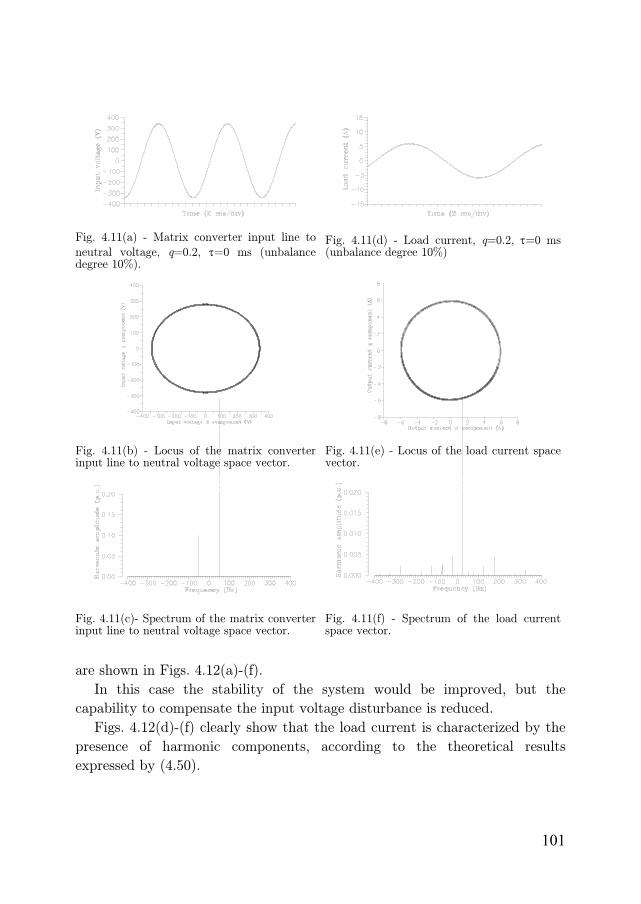
101
are shown in Figs. 4.12(a)-(f).
In this case the stability of the system would be improved, but the
capability to compensate the input voltage disturbance is reduced.
Figs. 4.12(d)-(f) clearly show that the load current is characterized by the
presence of harmonic components, according to the theoretical results
expressed by (4.50).
Fig. 4.11(a) - Matrix converter input line to
neutral voltage, q=0.2, τ=0 ms (unbalance degree 10%).
Fig. 4.11(d) - Load current, q=0.2, τ=0 ms (unbalance degree 10%)
Fig. 4.11(b) - Locus of the matrix converter input line to neutral voltage space vector.
Fig. 4.11(e) - Locus of the load current space vector.
Fig. 4.11(c)- Spectrum of the matrix converter input line to neutral voltage space vector.
Fig. 4.11(f) - Spectrum of the load current space vector.

102
A further simulation has been carried out considering as input voltage
perturbation a 5th harmonic component, having amplitude of 10% of the
fundamental component.
The system behaviour has been firstly evaluated without the digital low-
pass input voltage filter ( 0=τ ), and then in presence of the filter.
The results obtained are illustrated in Figs. 4.13 and 4.14, respectively. In
the case of 0=τ (Fig. 4.13) the system compensate the input voltage
disturbance and the load current is practically sinusoidal.
Fig. 4.12(a) – Matrix converter input line to
neutral voltage, q=0.2, τ=0.4 ms (unbalance degree 10%).
Fig. 4.12(d) – Load current, q=0.2, τ=0.4 ms (unbalance degree 10%).
Fig. 4.12(b) – Locus of the matrix converter input line to neutral voltage space vector.
Fig. 4.12(e) – Locus of the load current space vector.
Fig. 4.12(c)–Spectrum of the matrix converter input line to neutral voltage space vector.
Fig. 4.12(f) – Spectrum of the load current space vector.

103
In the case of τ = 0.4 ms (Fig. 4.14) the input voltage disturbance is
partially reflected at the output side, and the output current is characterized
by the presence of harmonic components, as predicted by (4.50) and shown in
Fig. 4.14(f).
Fig. 4.13(a) - Matrix converter input line to
neutral voltage, q=0.2, τ=0 ms (10% 5th harmonic).
Fig. 4.13(d) - Load current, q=0.2, τ=0 ms (10% 5th harmonic).
Fig. 4.13(b) - Locus of the matrix converter input line to neutral voltage space vector.
Fig. 4.13(e) - Locus of the load current space vector.
Fig. 4.13(c)-Spectrum of the matrix converter input line to neutral voltage space vector.
Fig. 4.13(f) - Spectrum of the load current space vector.

104
4.11. Important Remarks About Stability
Actually, stability issues of power converters and electrical drives have
been already discussed in several papers [43]-[47]. With reference to matrix
converters it is worth noting that the possibility of unstable behaviour is not
inherent in matrix converter operation, but rather related to the control
algorithm implementation. It has been previously mentioned that it is
Fig. 4.14(a) – Matrix converter input line to
neutral voltage, q=0.2, τ=0.4 ms. (10% 5th harmonic)
Fig. 4.14(d) – Load current, q=0.2, τ=0.4 ms. (10% 5th harmonic)
Fig. 4.14(b) – Locus of the matrix converter input line to neutral voltage space vector.
Fig. 4.14(e) – Locus of the load current space vector.
Fig. 4.14(c)– Spectrum of the matrix converter input line to neutral voltage space vector.
Fig. 4.14(f) – Spectrum of the load current space vector.

105
opportune to calculate the duty-cycles of the switching configurations on the
basis of the instantaneous values of the input voltages when studying the
operation of matrix converters under unbalanced and distorted supply
voltages. The feedforward action of this type of control is the main potential
reason of the instability phenomena. It has been also shown that the power
limit can be sensibly improved if the calculation of the duty-cycles is carried
out using filtered values of the matrix converter input voltages.
In practical applications, the instability phenomena could be not observed
if the voltage measurement is performed at the input of the L-C filter, rather
than at the input of the converter. In this case the system stability is
improved because the filtering action performed by the proposed digital filter
is replaced, to some extent, by the filter inductance Lf. Actually, instability is
not eliminated, but only moved towards higher power levels.
However, it can be noted that the voltage measurement at the L-C filter
input is not an optimal solution owing to the following reasons:
- The L-C filter is usually designed in order to satisfy EMC requirements
rather than to guarantee the system stability. In addition, it determines a
sensible phase-shift in the measured voltage at the fundamental frequency,
which can deteriorate the output voltage since the duty-cycles are not
calculated on the basis of the actual voltage.
- The digital filter, instead, can be tuned so that the system shows the
best performance and, in addition, it is implemented in the synchronous
reference frame, thus introducing no phase shift at the fundamental
frequency.
- If the matrix converter is connected to a weak network, the filter
inductance can be omitted because the grid inductance is sufficient for the
filter requirements; it is then possible to avoid the presence of a bulky
component. In this case the matrix converter stability can be improved only
by using the digital low-pass filter applied to the voltages measured across
the filter capacitors.
The effects introduced by digital controllers, such as the sample and hold
circuit and the switching period delay, also affect the stability of matrix
converters. The digital controller samples the input voltages at the beginning
of the cycle period, then calculates the duty-cycles of the switching
configurations that will be applied at the beginning of the next cycle period,

106
thus determining a delay of one cycle. It has long been known that a time
delay could remarkably modify the stability of the drive system.
The proposed analytical approach does not take into account the effect of
the control delay and therefore it gives reliable results only for low values of
the cycle period. The value of 80μs adopted in the numerical simulations is
sufficient for the implementation of the control algorithm and provides
results in good agreement with the theoretical analysis. In [52] it has been
clearly emphasized the influence of the cycle period width on the stability of
the drive system.
A further issue, relevant for the system stability, is the energy losses in
the input filter and in the converter switches, which influence the damping
capability of the drive system. In fact the energy losses can reduce the
voltage and current oscillations so improving the system stability.
For this purpose the behaviour of the matrix converter has been also
verified using the electronic circuit analysis program MICRO-CAP 7.0. In
this program it is possible to use more accurate models of the power switches
and then to improve the simulation reliability. The models adopted for
IGBTs and diodes are MICRO-CAP general models: IGBT type
IRG4PH50U, diode type HFA16PB120.
The matrix converter control technique and the system parameters are the
same used in the previous paragraph.
Fig. 4.15 shows the transition from stable to unstable operation of the
matrix converter obtained increasing the voltage transfer ratio q, for a given
value of the filter time constant (τ=0.2 ms). The upper traces represent the
input and output current waveforms, the medium trace is the voltage
measured at the input side of the L-C filter, and the bottom trace is the
voltage measured across the filter capacitance. As can be seen, the system is
stable for q=0.3 and unstable for q=0.7, in perfect agreement with Fig. 4.7.
For q=0.5 the system shows a stable behaviour, although the voltage
transfer ratio is slightly greater than the stability limit of Fig. 4.7. This can
be explained by the damping introduced by the energy losses and the effect
of the cycle period delay.

107
4.12. Conclusion
The MC can be considered as a current source at the input side, then a L-
C filter topology is needed to smooth the input currents and to satisfy the
EMI requirements. A reactive current flows through the input filter capacitor
of the matrix converter, which causes a reduction of the power factor
especially at low output power. As a consequence, the capacitor should be
chosen in order to ensure at least a power factor of 0.8 with 10% of the rated
output power. After the selection of the capacitor, the input filter inductance
can be selected in order to satisfy the IEEE Recommended Practices and
Requirements for Harmonic Control in Electrical Power Systems (IEEE Std.
519-1992).
If the input filter is well designed, current harmonics at frequencies greater
or equal to the switching frequency are smoothed to a certain extent. On the
30.000m 40.000m 50.000m 60.000m 70.000m 80.000m 90.000m 100.000m 110.000m 120.000m 130.000m 140.000m -50.000 -40.000 -30.000 -20.000 -10.000
0.000 10.000 20.000 30.000 40.000 50.000
30.000m 40.000m 50.000m 60.000m 70.000m 80.000m 90.000m 100.000m 110.000m 120.000m 130.000m 140.000m -800.000 -600.000 -400.000 -200.000
0.000 200.000 400.000 600.000 800.000
q=0.3 q=0.5 q=0.7(a)
(b)
(c)
30.000m 40.000m 50.000m 60.000m 70.000m 80.000m 90.000m 100.000m 110.000m 120.000m 130.000m 140.000m -800.000 -600.000 -400.000 -200.000
0.000 200.000 400.000 600.000 800.000
(d)
Fig. 4.15 - Transition from stable to unstable operation changing q from 0.3 to 0.5 and then to
0.7, with τ=0.2 ms. a) output current, b) input current, c) filter input voltage, d) matrix converter input voltage.

108
other hand, current harmonics at a frequency close to the resonance
frequency of the filter could be amplified determining oscillations of the
voltage across the capacitor, which in turn have a negative effect on the MC
behaviour leading to possible unstable operating conditions.
In order to increase the system stability it is possible to add a damping
resistance in parallel with the filter inductance. A suitable value of this
resistance allows the high frequency current harmonics to close through the
source leading to lower oscillations of the capacitor voltage. The damping
effect and then the stability limit increases while reducing the value of the
resistance. Unfortunately, this solution is effective for improving the MC
stability but it is of detriment for the EMI requirements. Therefore, a
compromise should be find between stability and input current quality.
A different approach which avoids the need of damping resistances is to
calculate the duty cycles of the MC switching configurations by means of
input voltage values filtered by a low-pass filter implemented in a
synchronous reference frame. This method has been proved to be very
effective for increasing the power limit and is included in the control scheme
of the MC analyzed in this chapter.
In this chapter a method for the stability analysis of matrix converters has
been proposed. For this purpose a variable state average model of the whole
system, including the grid impedance, the input L-C filter and the load, has
been derived, and the stability of the system has been evaluated by analyzing
the migration of the eigenvalues of the linearized state matrix.
By using the proposed approach, the maximum output power can be
calculated as function of the digital low-pass filter time constant, for given
values of the grid impedance, input L-C filter parameters and load.
Simulation results have been performed showing the validity of the proposed
method for low values of the cycle period, and emphasizing the improvement
of the power limit achievable by changing the time constant of the digital
low-pass filter.

109
5.Chapter 5 Advanced Models for Stability Analysis Abstract
In this chapter a theoretical analysis of the stability of matrix converters
is presented with the aim of predicting possible critical operating conditions.
It is verified that all the system parameters affect more or less the stability,
including the delay introduced by the digital controller and the power losses.
The theoretical analysis is supported by numerical simulations and
experimental results carried out on a matrix converter prototype.
5.1. Introduction
In chapter 4, MC stability has been investigated through a small signal
analysis of the whole system composed by the power grid, the input filter, the
MC and the load. It has been shown that the power limit is related to all

110
system parameters, and in particular to the grid impedance and the input L-
C filter parameters.
In addition, the analysis has been further developed showing that the
power limit can be increased if the duty-cycles of the switching configurations
are calculated using input voltages filtered by a digital low-pass filter
implemented in a synchronous reference frame. Using this filter the capability
of the matrix converter to compensate input voltage disturbances is affected
to some extent, but the stability limit can be sensibly improved. It has been
also verified that including a damping resistance in the input filter allows a
significant increase of the stability limit.
However, up to now, the analysis has neglected that the control of matrix
converter is usually achieved with a digital microprocessor, whose
calculations are performed within a finite cycle period. The digital processor
samples the input voltages and determines the configuration of the matrix
converter switches that are modified at the beginning of the next cycle
period, thus determining one cycle delay.
It has long been known that a time delay could remarkably modify the
system stability.
The analytical approach proposed in Chapter 4 does not take into account
the effect of the control delay and therefore it gives reliable results only for
low values of the cycle period.
In [52] the effects due to the presence of a sample and hold circuit and a
cycle period delay in the digital control of MCs have been investigated using
a small signal analysis combined with a frequency domain analysis. It has
been shown that, depending on the system parameters, the cycle period value
affects more or less the power limit. The presence of unstable operation in
MCs has been also documented in [25], where the same small signal analysis
as proposed in [18],[53] has been used. In particular, the effect of filtering
differently the magnitude and the phase angle of the input voltage vector has
been investigated. The existence of potential unstable operating conditions
has been experimentally proved, emphasizing the influence of the system
parameters.
In the first part of this chapter a complete analysis of the MC stability
taking account of all the system parameters including the input voltage filter
and the effects of the digital control is presented. The analysis is developed in

111
the frequency domain, using a small signal analysis similar to that carried out
in [52]. The new contribution is the analytical approach proposed for the
analysis of MC stability, which makes it possible to demonstrate the
existence of possible unstable operating conditions and to emphasize which
parameters may affect, more or less, the stability power limit. It has been
verified that, besides the system parameters, also the power losses must be
considered in order to predict the stability limit of matrix converter.
Despite of its completeness, the proposed method uses a small-signal
analysis that makes difficult the interpretation of the physical phenomena
related to instability.
During the study of instability phenomena, initially, it is possible to
observe small high frequency oscillations superimposed on the input voltages.
Then, owing to the effects of these oscillations on the calculations of the
duty-cycles, the amplitude of the voltage oscillations increases preventing the
normal operation.
In the second part of this chapter a different approach is presented for the
analysis of the MC stability, which is based on a large signal analysis carried
out in the frequency domain. The main advantage of this approach is the
easy comprehension of the instability origin and the possibility to relate the
amplitude of the input voltage oscillations to the operating conditions.
As the proposed analysis is based on a large-signal model, it is possible to
investigate the non-linear behaviour of MCs in the case of large input voltage
perturbations. This allows explaining phenomena that have not been clearly
understood until now, such as the unstable behaviour of MCs in terms of
limit cycles.
Several numerical simulations are presented showing current and voltage
waveforms under stable and unstable operating conditions. Finally,
experimental results carried out on a MC prototype are given for supporting
the theoretical analysis and for proving the effect of different filtering
methods applied to the input voltages.
5.2. Input/Output Matrix Converter Performance
The whole system, which is composed by a power supply, a second order
input R-L-C filter, and a matrix converter feeding a R-L passive load, is
represented in Fig. 5.1, where space vector notation is used for the

112
representation of the system variables.
In this paragraph the main equations related to the system represented in
Fig. 5.1 will be introduced. As usual, the analytical developments are carried
out neglecting the effects of the switching harmonics, considering for the
output voltages and input currents their average values over a cycle period
Tp.
The variable t, s and z will be used to distinguish between the time
domain, the Laplace domain and the domain of the sampled signal,
respectively.
With reference to Fig. 5.1, the equation for the input side of the converter,
written in the Laplace domain, is as follows:
)()()()( svsisZsv iieq += (5.1)
where )(sveq and )(sZ are the equivalent voltage and the impedance of the
voltage source and the input filter, considered as a single bipole.
The equation of the output side of the converter can be expressed as
follows
)()()( svsYsi oo = (5.2)
where )(sY is the admittance of the passive linear load.
The input-output relationships (2.35)-(2.36) of the matrix converter,
written using the duty-cycle space vectors dm and im [7], are here reported
for convenience:
ii
Matrix inverter
Rs Ls RL LL
Non ideal voltage supply Input filter Load
ivsv
Digital controller
id mm ,
Lf
Cfov oi
Rf
Fig. 5.1 - Basic matrix converter scheme.

113
[ ])()()()(2
3)( ** tvtmtvtmtv idiio += (5.3)
[ ])()()()(2
3)( * titmtitmti odoii += . (5.4)
The symbol ‘*’ is used to represent complex conjugate variables.
If the input current vector is kept in phase with the input voltage vector,
the problem of the determination of the duty-cycle space vectors is
completely solved by the following equations:
)(3
)()(
*
,
,tv
tvtm
i
refo
refd = (5.5)
)(3
)()(
*
*,
,tv
tvtm
i
refo
refi = . (5.6)
where )(, tv refo is the reference output voltage.
Unfortunately, at any instant t the duty-cycles )(tmd and )(tmi cannot
have exactly the values )(, tm refd and )(, tm refi because the digital controller,
which measures the input voltages and calculate (5.5) and (5.6) at each cycle
period, applies the new switching configurations only at the beginning of the
next cycle period, thus introducing a time delay. This means that )(tmd and
)(tmi are delayed with respect to the desired values.
The model represented in Fig. 5.2 has been developed to take into account
the effects of the control system delay. S&H is a sample and hold device, z--1
is the delay operator and ZOH a zero-order hold.
It should be noted that, using this model, )(tmd and )(tmi in (5.3) and
(5.4) are constant during a cycle period Tp, while the input voltage vector
Z-1 ZOHrefim ,
refdm ,
im
dm
S&H
Fig. 5.2 - System used to represent the effect of the digital controller.

114
)(tvi and the output current vector )(tio are free to change.
According to Fig. 5.2, the relationship between )(tmd and )(, tm refd or
between )(tmi and )(, tm refi can be described through the transfer function
)(sD in the Laplace domain given by
sT
p
sT
refi
i
refd
d p
p
esT
e
sm
sm
sm
smsD
−−
⎟⎟⎠
⎞⎜⎜⎝
⎛ −===
1
)(
)(
)(
)()(
,,
. (5.7)
In (5.7) the term inside the brackets is related to the sampling and
reconstruction processes, whereas the exponential term outside the brackets is
due to the delay introduced by the digital controller.
In order to study the stability of the system, it is opportune to linearize
the system equations around a steady-state operating point corresponding to
balanced and sinusoidal supply voltages.
5.3. Steady-State Operating Conditions with Balanced and Sinusoidal Supply Voltages
In steady-state operating conditions, with balanced and sinusoidal supply
voltages, the input voltages and the reference output voltages can be
represented by means of rotating space vectors with constant magnitudes, as
follows:
tjii
ieVtV ω=)( (5.8)
tjreforefo
oeVtV ω= ,, )( (5.9)
where ωi and ωo are the input and output angular frequency, respectively.
Substituting (5.8) and (5.9) in (5.5) and (5.6), leads to the following
steady-state expressions for )(, tm refd and )(, tm refi :
tj
i
refo
refdoie
V
VtM )(
*
,
,3
)( ω+ω= (5.10)

115
tj
i
refo
refioie
V
VtM )(
*
*,
,3
)( ω−ω= . (5.11)
The actual values of the duty-cycle space vectors dM and iM could be
calculated applying (5.7) to (5.10) and (5.11), respectively. It is worth noting
that the delay introduced by the digital filter on the fundamental harmonics
at frequencies ωi and ωo can be ignored and the actual values of the duty-
cycle space vectors dM and iM can be assumed equal to their reference
values refiM , and refdM , . On the basis of this assumption, substituting (5.10)
and (5.11) in (5.3), and taking (5.8) into account, it is possible to verify that
also the output voltage can be assumed equal to its reference value
)()( , tVtV refoo = . (5.12)
As a consequence, the steady-state output current vector can be expressed
as
tjo
tjrefooo
oo eIeVYtI ωω =ω= ,)()( (5.13)
where
2
,
3
2
ref
refo
idoV
VPI γ= (5.14)
{ })(Re
)(
o
o
Y
Y
ωω
=γ (5.15)
)()(2
3, tItVP orefoid ⋅= . (5.16)
In (5.14) and (5.16) Pid is the power delivered to the load by an ideal
matrix converter in which )()( , tVtV refoo = .
5.4. Small Signal Equations
The stability analysis is performed under the assumption that a small
perturbation ivΔ is superimposed on the input voltage space vector.
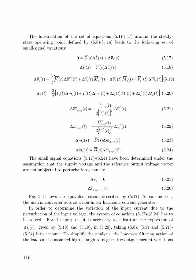
116
The linearization of the set of equations (5.1)-(5.7) around the steady-
state operating point defined by (5.8)-(5.16) leads to the following set of
small-signal equations:
)()()(0 svsisZ ii Δ+Δ= (5.17)
)()()( svsYsi oo Δ=Δ (5.18)
[ ])()()()()()()()(2
3)( **** tmtVtMtvtMtvtmtVtv didiiiiio Δ+Δ+Δ+Δ=Δ (5.19)
[ ])()()()()()()()(2
3)( ** tMtitMtitmtItmtIti doiodoioi Δ+Δ+Δ+Δ=Δ (5.20)
[ ] )()(3
)()( *
2*
,
, tvtV
tVtm i
i
refo
refd Δ−=Δ (5.21)
[ ] )()(3
)()( *
2*
*,
, tvtV
tVtm i
i
refo
refi Δ−=Δ (5.22)
)()()( , smsDsm refdd Δ=Δ (5.23)
)()()( , smsDsm refii Δ=Δ . (5.24)
The small signal equations (5.17)-(5.24) have been determined under the
assumption that the supply voltage and the reference output voltage vector
are not subjected to perturbations, namely
0=Δ sv (5.25)
0, =Δ refov . (5.26)
Fig. 5.3 shows the equivalent circuit described by (5.17). As can be seen,
the matrix converter acts as a non-linear harmonic current generator.
In order to determine the variation of the input current due to the
perturbation of the input voltage, the system of equations (5.17)-(5.24) has to
be solved. For this purpose, it is necessary to substitute the expression of
)(sioΔ , given by (5.18) and (5.19), in (5.20), taking (5.8), (5.9) and (5.21)-
(5.24) into account. To simplify the analysis, the low-pass filtering action of
the load can be assumed high enough to neglect the output current variations

117
due to the output voltage variations, yielding
0=Δ oi . (5.27)
Under this assumption, substituting (5.12), (5.14), (5.21)-(5.24) in (5.20)
leads to the following expression for the variation of the input current in the
Laplace domain:
[ ] )2()(3
2)(
2* icieq
i
idi jsvsD
V
Psi ω−Δ−=Δ (5.28)
where )(sv ciΔ is the Laplace transform of )(* tviΔ and )(sDeq is defined by
[ ])()(2
1)( *
ooeq jsDjsDsD ω+γ+ω−γ= . (5.29)
The superscript ”c” applied to the function ivΔ is used to represent the
Laplace transform of the conjugate of ivΔ . More details on this mathematical
representation, that will be used in the following, can be found in Appendix
C. It can be verified that for angular frequencies much higher than ωo,
)()( ω≅ω jDjDeq .
It is possible to determine the fundamental equation that must be satisfied
by the input voltage variation substituting (5.28) in (5.17), yielding
[ ] 0)()2()()(3
22*
=Δ+ω−Δ− svjsvV
PsDsZ ii
ci
i
ideq . (5.30)
In the previous equation there are two unknowns, which are ivΔ and civΔ .
Hence, to solve the problem, a further equation is needed. This equation can
be found by applying the operator ”c” to (5.30), leading to
ivΔ)(sZ )(siiΔ
Fig. 5.3 - Equivalent circuit of the system for small signal analysis.

118
0)()2()()(3
22
=Δ+ω+Δ− svjsvV
PsDsZ c
iii
i
idceq
c . (5.31)
To simplify (5.30) and (5.31) it is useful to introduce a rotating reference
frame synchronous with the supply voltage, which is completely defined
substituting the variable s with
s = u + jωi . (5.32)
The following set of equations, written in matrix form, can be determined
introducing (5.32) in (5.30) and (5.31), yielding:
⎥⎦
⎤⎢⎣
⎡=⎥
⎦
⎤⎢⎣
⎡ω−Δω+Δ
0
0
)(
)(),(
ici
ii
idjuv
juvPuM (5.33)
where
⎥⎥⎥⎥
⎦
⎤
⎢⎢⎢⎢
⎣
⎡
ω−−
ω+−=
1)(3
2)(
)(3
21
),(
2
2*
i
idi
ceq
i
idieq
id
V
PjuZ
V
PjuZ
PuM (5.34)
and
)()()( sDsZsZ eqeq = . (5.35)
By means of the previous analytical developments, the small signal
equations (5.17)-(5.24) have been summarized by (5.33)-(5.35), which
completely describe the system response due to a small input voltage
variation.
Analyzing (5.35) it can be concluded that the behaviour of the system is
described by the equivalent grid impedance eqZ , given by a combination of
the actual impedance and the transfer function of the delay introduced by
the digital controller.
5.5. Stability Analysis
Due to presence of the controller delay, the system stability cannot be
analyzed through the determination of the system poles, because the

119
characteristic equation does not have a polynomial form. The instability
phenomena that can be observed in matrix converters are generally
characterized by the presence of sinusoidal oscillations superimposed to the
input voltage. Therefore it is possible to determine an equation representing
the necessary condition for the existence of unstable operation writing (5.33)
in the form of an harmonic balance. For this purpose the variable u = jω
must be introduced in (5.33) yielding
⎥⎦
⎤⎢⎣
⎡=⎥
⎦
⎤⎢⎣
⎡ω−ωΔω+ωΔ
ω0
0
)(
)(),(
ici
ii
idjjv
jjvPjM . (5.36)
The set of equations (5.37) has a non-trivial solution only if the
determinant of M is zero, leading to the following constraint equation:
13
2)(
2
2=⎟⎟
⎠
⎞⎜⎜⎝
⎛ωΓ
i
id
V
P (5.37)
where
)()()( iceqieq jjZjjZ ω−ωω+ω=ωΓ . (5.38)
A necessary condition for (5.37) to be verified is the existence of an
angular frequency ωr satisfying the following constrain equation:
0)(arg =ωΓ r . (5.39)
According to (5.39), for ω equal to ωr the function )(ωΓ is a real positive
number, having the dimension of the square of an impedance. It is then
useful to define a new equivalent resistance given by
)( rresR ωΓ= . (5.40)
Substituting (5.40) in (5.37) and solving for Pid leads to the following
value of the ideal power limit:
res
iid,lim
R
VP
2
2
3= . (5.41)
As can be seen from (5.41), the maximum power limit is proportional to

120
the square of the input voltage and to the inverse of the equivalent resistance
Rres.
To outline how the stability analysis can be applied, an example is
discussed in the following.
The first step is to plot )(ωΓ as a function of ω. The most significant
range of frequencies is centred around the resonance frequency of the input L-
C filter (including the grid inductance too), as it corresponds to the highest
magnitudes of the function )(ωΓ . Fig. 5.4 shows the behaviour of )(ωΓ with
reference to the parameters given in Tab. 5.1 and for a cycle period Tp of
80μs.
Fig. 5.4(a) shows the magnitude of )(ωΓ , whereas the argument of )(ωΓ ,
normalized in the range [-π, π], is shown in Fig. 5.4(b). It can be noted that
the argument of )(ωΓ equals zero for several angular frequencies, i.e. ’rω and
’’rω . Obviously, the stability power limit has to be evaluated with reference to
the worst case, corresponding to the highest magnitude of )(ωΓ . Among all
the solutions, )(ωΓ assumes the maximum value for ’rω=ω , as can be
verified in Fig. 5.4(a). Then, the equivalent resistance Rres must be calculated
assuming ’rr ω=ω in (5.40). Once Rres is known, the stability power limit can
be determined by means of (5.41).
In order to emphasize how the delay of the digital controller can improve
the stability power limit, a further example is discussed with reference to an
ideal controller with a cycle period Tp=0. In this case the behaviour of )(ωΓ
is illustrated in Fig. 5.5. The stability power limit, corresponding to the
angular frequency ’’’rω , is sensibly lower compared with the one determined
TABLE 5.1 - SYSTEM PARAMETERS
Supply
VS = 110 V(rms),
ωi = 2π 50 rad/s,
RS = 0.55 Ω, LS=0.90 mH
Filter
Lf = 1.16 mH, Cf = 4.5 μF
Rf = 300 Ω
Load
RL= 8.2 Ω, LL = 1.3 mH,
ωo = 2π 100 rad/s

121
for a non-ideal controller. It is clear, comparing Fig. 5.5 to Fig. 5.4, that the
delay introduced by the digital controller has the effect to modify the
)(arg ωΓ curve, whereas the magnitude is practically the same in both cases.
Owing to the delay, the argument of )(ωΓ shown in Fig. 5.4(b) reaches
zero at ’rω , that is much lower than ’’’
rω . As a consequence, also the
equivalent resistance Rres is lower, leading to a higher stability power limit.
Further details on the effect of the digital delay have been discussed in [52].
5.6. Small Signal Equations Introducing a Digital Filter
The power limit can be sensibly improved if the calculation of the duty
cycles is carried out by filtering the matrix converter input voltages [24].
The equation of this filter, written in terms of Laplace transform, can be
expressed as:
)()(1
1)()()( sv
jssvsFsv i
i
iif ω−τ+== (5.42)
where )(svif is the Laplace transform of the filtered input voltage vector.
Owing to the discretization introduced by the digital controller, the
transfer function )(sF in (5.42) can be only approximated by a Z-transform
)(zFd . The expression of )(zFd varies on the basis of the method used to
0.1 1
10 100
1 . 10 3 1 . 10 4 1 . 10 5
0 5000 1 .104 1.5 .104 2 .1043.14 1.57
0 1.57 3.14
ω
)(ωΓ
)(arg ωΓ
a)
rω′
rω′′
b)
0.1
1
10
100
1 .1031 .104
1 .105
0 5000 1 .104 1.5 . 10 4 2 . 10 4 3.14
1.57
0
1.57
3.14
ω
)(ωΓ
)(arg ωΓ
a)
rω ′′′
b)
Fig. 5.4 – Behaviour of )(ωΓ for the
system parameters of Tab. I, with the effects of the digital controller delay, a) magnitude, b) argument .
Fig. 5.5 – Behaviour of )(ωΓ for the system
parameters of Tab. I, without the effects of the digital controller delay, a) magnitude, b) argument .

122
obtain the discrete-time formulation. The expression of )(zFd used in this
chapter is given in Appendix D. On the other hand, the analysis is developed
in the Laplace domain, then it is necessary to represent )(zFd in terms of
Laplace transform, introducing the transfer function )(sFa . It is known that
the expression of )(sFa can be determined from )(zFd introducing Tsez = ,
leading to
)()( Tsda eFsF = . (5.43)
On the basis of (5.43), the variation of the filtered voltage in terms of
Laplace transform can be approximated as follows:
)()()( svsFsv iaif Δ=Δ (5.44)
The approximation consists in neglecting the harmonic components of
)(sviΔ at a frequency comparable with or greater than the sampling
frequency. In the system under study this assumption can be made because
the input filter is of low-pass type.
Using the same procedure described in Paragraph 5.4, in which the input
voltage variation )(sviΔ is replaced by )(svifΔ , leads to the following
expression for the input current variation:
[ ] )2()2()(3
2)(
2* icii
caeq
i
idi jsvjsFsD
V
Psi ω−Δω−−=Δ . (5.45)
It can be noted that (5.45) corresponds to (5.28), the only difference is the
presence of the transfer function )2( ic
a jsF ω− which multiplies the term
)(sDeq . As a consequence, the stability analysis carried out in Paragraph 5.5
is still valid provided that the equivalent impedance (5.35) is replaced with
the following expression:
)2()()()( ic
aeqeq jsFsDsZsZ ω−= . (5.46)
The presence of the transfer function )2( ic
a jsF ω− modifies the equivalent
impedance reducing its magnitude and changing its argument. If the filter is

123
correctly designed, this effect determines a reduction of the equivalent
resistance (5.40) with an effective improvement of the stability power limit.
5.7. Model for the MC Losses
The power limit that can be calculated by means of the equations
presented in the previous paragraphs is generally lower than that achievable
in experimental tests. This because several factors, such as the iron losses in
the inductances, or the power losses of the converter, may increase the
damping effect of the real system, thus preventing unstable oscillations to
arise.
In this paragraph a simplified method to represent the effects of the
converter power losses on the system stability is proposed.
A non-ideal converter can be generally represented using a simplified
model composed by an ideal converter and two generators that take into
account the converter power losses, i.e. switching losses and conduction
losses. The converter model that will be used in this chapter is represented in
Fig. 5.6.
The output voltage is usually lower than the reference voltage since there
is a voltage drop on the static switches. This voltage drop mainly determines
the amount of the conduction losses )(tpcd , and the voltage cdv can be
defined as follows:
)()(
)(
3
2)(
2ti
ti
tptv o
o
cdcd = . (5.47)
Due to the switching losses )(tpsw , the current at the input side of the
non-ideal converter is generally higher than that of the ideal converter. This
Ideal
Matrix Converter
+
swi
cdv
outvov
iiini oi
Fig. 5.6 - Basic scheme of a non-ideal matrix converter.

124
behaviour can be modelled with a current generator swi defined by
)()(
)(
3
2)(
2tv
tv
tpti i
i
swsw = . (5.48)
The voltage generator in (5.47) and the current generator in (5.48) are
defined so that they absorb an active power equal to pcd and psw, respectively.
The presence of the power losses must be included in the small signal
equations with the aim of predicting the power limit with more accuracy. In
order to linearize (5.47) and (5.48), it is firstly necessary to determine the
equations of the system in steady-state operating conditions with balanced
and sinusoidal supply voltages. It is useful to represent the steady-state
values of pcd and psw introducing two equivalent resistances as follows
2
2
3ocdcd IRP = . (5.49)
sw
isw
R
VP
2
2
3= . (5.50)
Substituting (5.49) in (5.47) yields
)()( tIRtV ocdcd = (5.51)
which demonstrates that at the fundamental frequency the conduction losses
have the same effect as an additional resistance Rcd connected in series with
the load. Therefore, (5.13)-(5.17) are still valid if the load admittance at
angular frequency ωo is replaced by the following expression:
)(1
)()(
ocd
ooeq
jYR
jYjY
ω+ω
=ω . (5.52)
According to this approach, the main effect of the conduction losses is the
reduction of the steady-state load current and, consequently, of the input
current. The presence of switching losses, instead, does not modify anyone of
the steady-state equations determined in Paragraph 5.15. Once the steady-
state conditions have been determined, in order to proceed along with the
linearization of (5.47) and (5.48), a model for the converter losses is needed.
The switching losses are proportional to the input voltage and the output

125
current, while the conduction losses are proportional to the output current
[54]. Then, the simplest model for the converter losses can be represented by
the following equations:
ocdcd iktp =)( (5.53)
oiswsw ivktp =)( (5.54)
where kcd and ksw are constant.
Taking (5.54) and (5.55) into account, the small signal equations
corresponding to (5.47) and (5.48) are as follows:
0=Δ cdv (5.55)
)())((3
)(3
)( *
2*2tv
tV
Ptv
V
Pti i
i
swi
i
swsw Δ−Δ=Δ (5.56)
The result expressed in (5.55) is justified by the fact that, according to
(5.27), the variation of the output current is negligible.
In (5.56) the switching losses Psw appear in both terms. In the first term
the switching losses can be expressed through (5.50), whereas in the second
term it is convenient to express the switching losses as a percentage of Pid
introducing the ratio ε (Appendix E) defined as
id
sw
P
P=ε . (5.57)
In this way it will be possible to define an equivalent impedance )(sZeq
similar to (5.35) and (5.46). Taking (5.57) and (5.50) into account, (5.56) can
be rewritten in the Laplace domain as follows:
)2()(3
)(2
1)(
2* ici
i
idi
sw
sw jsvV
Psv
Rsi ω−Δ
ε−Δ=Δ . (5.58)
The equivalent circuit of the switching losses represented by (5.58) is
shown in Fig. 5.7.
The equivalent circuit of the whole system can be determined combining
the equivalent circuit of Fig. 5.7 with the basic circuit of Fig. 5.3, leading to
Fig. 5.8.

126
It can be noted that the effect of the power losses can be described with a
resistance connected in parallel with the input impedance and with a current
generator. Fig. 5.8 can be simplified substituting the two current generators
with an equivalent single current generator giΔ , as shown in Fig. 5.9. Taking
(5.45) into account, giΔ can be expressed as
)2()2()(2)(3
2)(
2* icii
caeq
i
idg jsvjsFsD
V
Psi ω−Δ⎟
⎠⎞
⎜⎝⎛ ω−+
ε−=Δ (5.59)
The only difference between (5.59) and (5.45) is the presence of the term
ε/2 added to the term )2()( ic
aeq jsFsD ω− . Consequently, the stability analysis
carried out in Paragraph 5.5 is still valid provided that the equivalent
impedance (5.46) is replaced with the following expression:
( ) ⎟⎠⎞
⎜⎝⎛ ε
+ω−=2
)2()(2//)()( ic
aeqsweq jsFsDRsZsZ (5.60)
It can be verified that the magnitude of the function )(ωΓ , developed
through (5.60), is reduced owing to the presence of the resistance 2Rsw
connected in parallel with the input impedance. This effect leads to an
iniΔ
swR2 )()( * i
ci2
i
id j2svV3P
ω−Δε
−ivΔ
iiΔ
Fig. 5.7 - Equivalent circuit of the switching losses for small signal analysis.
ivΔ
iniΔ
)(sZ swR2 )2()(3 2* i
ci
i
id jsvVP
ω−Δε
− )(siiΔ
Fig. 5.8 - Equivalent circuit of a non-ideal matrix converter for small signal analysis.

127
improvement of the stability power limit as will be shown in the next
paragraphs.
In order to perform numerical and experimental tests on the stability of
matrix converters feeding a constant load, it is more opportune to use as
variable the output-to-input voltage transfer ratio q instead of Pid.
Combining (5.13)-(5.16) and (5.41) and solving for q leads to the following
value of the limit voltage transfer ratio:
{ })(Re
1
oeqres
lim
jYRq
ω= . (5.62)
It is evident in (5.62) that, as the conduction power losses reduce the
equivalent load admittance, they increase the limit voltage transfer ratio.
5.8. Simulation Results
In order verify the theoretical results obtained in the previous paragraphs,
the behaviour of the system represented in Fig. 5.1 has been tested by
numerical simulations.
For this purpose, the electronic circuit analysis program MICRO-CAP 7.0
has been adopted. In this program it is possible to use accurate models of the
power switches and then to improve the simulation reliability. The numerical
simulations take into account the switching behaviour of the matrix
converter and the delay related to the digital implementation of the control
algorithm.
The control strategy adopted for the matrix converter is the SVM
technique, with a double-sided switching pattern [7] and a cycle period of 80
μs. The values of the system parameters are shown in Tab. 5.1.
Firstly, the effect of the power losses has been neglected and the equations
ivΔ
iniΔ
)(sZ swR2 )(sigΔ
Fig. 5.9 - Equivalent circuit of a non-ideal matrix converter with a single current generator.

128
found in Paragraphs 5.16 and 5.17 have been used to evaluate the limit
voltage transfer ratio for different values of the cut-off frequency fcut-
off=1/(2πτ) of the input voltage digital filter. The corresponding results are
shown by the curve a) of Fig. 5.10.
Several simulations have been performed to check the validity of this
stability curve using ideal switches. For instance, Fig. 5.11 shows the
behaviour of the converter for q = 0.37 and fcut-off = 300 Hz (corresponding to
a time constant τ = 0.53 ms), which is represented by the point 1 in Fig.
5.10.
Fig. 5.11(a) shows the steady-state waveform of the input voltage of the
matrix converter. The steady-state waveforms of the line current and load
current are illustrated in Figs. 5.11(b) and (c), respectively. As is possible to
see, all the waveforms are sinusoidal and characterized by a small ripple, due
to the high switching frequency of the matrix converter.
Then, the voltage transfer ratio has been changed to 0.47 (point 2 in Fig.
5.10) and the corresponding converter behaviour is shown in Fig. 5.12. Fig.
5.12(a) shows the waveform of the input voltage, whereas the waveforms of
the line current and load current are illustrated in Figs. 5.12(b) and 5.12(c),
respectively. In these operating conditions the input voltage and the line
current waveforms are heavily distorted, showing large oscillations at about
1.75 kHz.
This behaviour is due to the predicted instability phenomena that occur
0
0,2
0,4
0,6
0,8
1
200 300 400 500
a)
b)
123
4
qlim
fcut-off
Fig. 5.10 - Limit voltage transfer ratio versus cut-off frequency of the input voltage digital filter with the system parameters given in Tab. I. a) without converter power losses, b) with converter power losses.
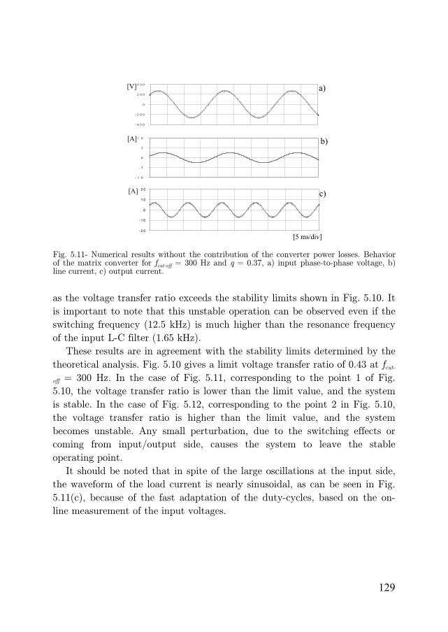
129
as the voltage transfer ratio exceeds the stability limits shown in Fig. 5.10. It
is important to note that this unstable operation can be observed even if the
switching frequency (12.5 kHz) is much higher than the resonance frequency
of the input L-C filter (1.65 kHz).
These results are in agreement with the stability limits determined by the
theoretical analysis. Fig. 5.10 gives a limit voltage transfer ratio of 0.43 at fcut-
off = 300 Hz. In the case of Fig. 5.11, corresponding to the point 1 of Fig.
5.10, the voltage transfer ratio is lower than the limit value, and the system
is stable. In the case of Fig. 5.12, corresponding to the point 2 in Fig. 5.10,
the voltage transfer ratio is higher than the limit value, and the system
becomes unstable. Any small perturbation, due to the switching effects or
coming from input/output side, causes the system to leave the stable
operating point.
It should be noted that in spite of the large oscillations at the input side,
the waveform of the load current is nearly sinusoidal, as can be seen in Fig.
5.11(c), because of the fast adaptation of the duty-cycles, based on the on-
line measurement of the input voltages.
- 4 0 0
- 2 0 0
0
2 0 0
4 0 0[V] a)
- 1 0
- 5
0
5
1 0[A]
- 2 0
- 1 0
0
1 0
2 0
[5 ms/div]
[A] c)
b)
Fig. 5.11- Numerical results without the contribution of the converter power losses. Behaviorof the matrix converter for fcut-off = 300 Hz and q = 0.37, a) input phase-to-phase voltage, b) line current, c) output current.
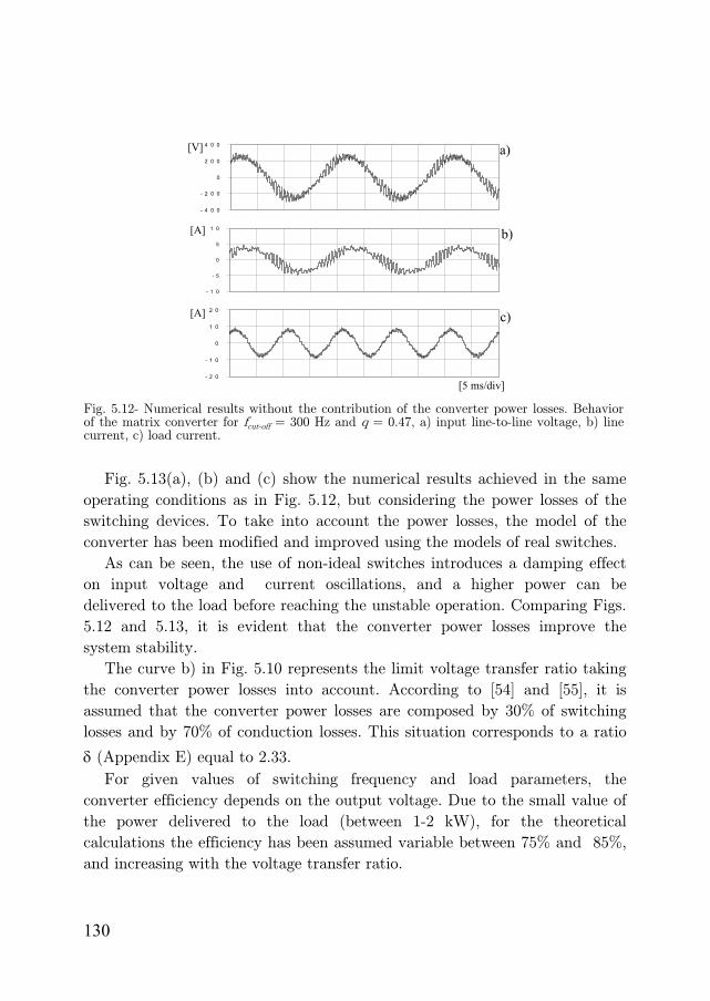
130
Fig. 5.13(a), (b) and (c) show the numerical results achieved in the same
operating conditions as in Fig. 5.12, but considering the power losses of the
switching devices. To take into account the power losses, the model of the
converter has been modified and improved using the models of real switches.
As can be seen, the use of non-ideal switches introduces a damping effect
on input voltage and current oscillations, and a higher power can be
delivered to the load before reaching the unstable operation. Comparing Figs.
5.12 and 5.13, it is evident that the converter power losses improve the
system stability.
The curve b) in Fig. 5.10 represents the limit voltage transfer ratio taking
the converter power losses into account. According to [54] and [55], it is
assumed that the converter power losses are composed by 30% of switching
losses and by 70% of conduction losses. This situation corresponds to a ratio
δ (Appendix E) equal to 2.33.
For given values of switching frequency and load parameters, the
converter efficiency depends on the output voltage. Due to the small value of
the power delivered to the load (between 1-2 kW), for the theoretical
calculations the efficiency has been assumed variable between 75% and 85%,
and increasing with the voltage transfer ratio.
- 2 0
- 1 0
0
1 0
2 0
- 1 0
- 5
0
5
1 0
- 4 0 0
- 2 0 0
0
2 0 0
4 0 0
b)
[V] a)
[A]
[5 ms/div]
[A] c)
Fig. 5.12- Numerical results without the contribution of the converter power losses. Behaviorof the matrix converter for fcut-off = 300 Hz and q = 0.47, a) input line-to-line voltage, b) line current, c) load current.

131
As can be seen from Fig. 5.10, the converter power losses have a strong
stabilizing effect and give an effective contribution to the system stability
improvement.
5.9. Experimental Results
In order to verify the proposed theoretical approach for the MC stability,
a prototype of a three-phase to three-phase matrix converter has been used to
supply a linear passive R-L load. The matrix converter is realized using the
FM35E12KR3 IGBT module produced by EUPEC. The control algorithm is
implemented on the platform C6000, a floating-point digital signal processor
provided by Texas Instruments. The switching frequency is 12.5 kHz,
corresponding to a cycle period of 80 μs. The converter is fed by a voltage
transformer with variable voltage transfer ratio to adjust the input voltage to
a value of about 110 V rms. A L-C filter is connected at the input side of the
converter. The parameters of filter, supply and load correspond to those
reported in Tab. 5.1.
Several tests have been performed, for different values of the cut-off
frequency of the input voltage digital filter and for different values of the
- 4 0 0
- 2 0 0
0
2 0 0
4 0 0
- 1 0
- 5
0
5
1 0
- 2 0
- 1 0
0
1 0
2 0
b)
[V] a)
[A]
[5 ms/div]
[A] c)
Fig. 5.13- Numerical results with the contribution of the converter power losses. Behavior of the matrix converter for fcut-off = 300 Hz and q = 0.47, a) input line-to-line voltage, b) line current, c) load current.

132
voltage transfer ratio.
Fig. 5.14 shows the behaviour of the matrix converter for fcut-off = 300 Hz
and q = 0.6. Fig. 5.14(a) represents the input voltage, Fig. 5.14(b) the line
current and Fig. 5.14(c) the load current, respectively. It is evident that the
system is stable, and only a small ripple due to the switching operation can
be seen.
In Fig. 5.15, the voltage transfer ratio has been increased up to 0.7. As
can be seen, the system becomes unstable, with appreciable oscillations on
both input voltage and line current. The frequency of these oscillations is
about 1700 Hz.
This results are in good agreement with the proposed theoretical
approach. In fact, the situation of Fig. 5.14 corresponds to point 3 in Fig.
5.10, that is inside the stability region, whereas the situation of Fig. 5.15
corresponds to point 4, that is outside the stability region.
It is important to make a final remark on the use of the mathematical
model proposed in this Chapter. The system parameters should be exactly
known in order to determine the power stability limit with sufficient
accuracy. Even small errors on the parameters values may lead to appreciable
mismatching between theoretical and experimental results.
a)
b)
c)
[V]
[A]
[A]
[5 ms/div]
-10
-5
0
5
10
-20
-10
0
10
20
-400
-200
0
200
400
Fig. 5.14 - Experimental tests. Behavior of the matrix converter for fcut-off = 300 Hzand q = 0.6, a) input line-to-line voltage, b) line current, c) load current.

133
However, the proposed approach has the merit of emphasizing the
mathematical relationships between the power stability limit and the system
parameters, being a useful tool for the comprehension of the phenomena
which occur in matrix converters.
5.10. Stability Analysis Based on a Large Signal Model
When instability phenomena are observed in MCs, as the output power is
increased over a limit value, initially, small low frequency oscillations
superimposed on the input voltages take place. Then, owing to the effects of
these oscillations on calculations of the duty-cycles, the amplitude of the
voltage oscillations increases preventing the normal operation.
Despite of its completeness, the analysis presented in the first part of this
chapter uses a small-signal approach [56], making difficult to interpret the
physical phenomena related to instability.
In the second part of this chapter a new approach is presented for the
analysis of the MC stability, which is based on a large signal analysis carried
out in the frequency domain. The main advantage of this approach is the
easy comprehension of the instability origin and the possibility to relate the
amplitude of the input voltage oscillations to the operating conditions.
a)
b)
c)
[V]
[A]
[A]
[5 ms/div]
-20
-10
0
10
20
-20
-10
0
10
20
-400
-200
0
200
400
Fig. 5.15 - Experimental tests. Behavior of the matrix converter for fcut-off = 300 Hz and q = 0.7, a) input line-to-line voltage, b) line current, c) load current.
134
As the proposed analysis is based on a large-signal model, it is possible to
investigate the non-linear behaviour of MCs in the case of large input voltage
perturbations. This allows one to explain phenomena that have not been
clearly understood until now, such as the unstable behaviour of MCs in terms
of limit cycles.
Several numerical simulations are presented showing current and voltage
waveforms under stable and unstable operating conditions. Finally,
experimental results carried out on a MC prototype are given for supporting
the theoretical analysis and for proving the effect of different filtering
methods applied to the input voltages. It is expected that these results will
be useful in the design of matrix converter systems in the future.
5.11. Equations of the System
As is known, the matrix converter allows not only the control of the
output voltages, but also of the phase angle of the input current vector.
If the switches are assumed ideal and the converter power losses are
neglected, the input current vector can be expressed in terms of the power po
delivered to the load as shown in (1.4):
As usual, the input current vector is supposed to be in phase with the
actual input voltage vector, determining instantaneous unity input power
factor,
iref v=ψ . (5.63)
Substituting (3) in (1.4) leads to the following expression for the input
current:
*
)(
3
2
i
oi
v
tpi = . (5.64)
The magnitude of the input current space vector depends on the output
power level and the input voltage vector.
With reference to Fig. 5.1, the equation for the input side of the MC,
written in the Fourier domain, is reported in (5.1).
The behaviour of the system at the input side is completely described by
(4.1) and (5.1) once the output power is assigned.

135
A. Expression of the Input Voltage
In order to introduce the problem of the stability of matrix converter, it is
opportune to discuss the results of some numerical simulations. For this
purpose, the electronic circuit analysis program MICRO-CAP 7.0 has been
adopted. In this program it is possible to use accurate models of the power
switches and then to improve the simulation reliability. The numerical
simulations take into account the switching behaviour of the matrix
converter and the delay related to the digital implementation of the control
algorithm. The control strategy adopted for the matrix converter is the SVM
technique, with a double-sided switching pattern [7] and a cycle period of 80
μs. The values of the system parameters are shown in Tab. 5.2.
The behaviour of a matrix converter in stable operating conditions is
shown in Fig. 5.16 referring to a input-to-output voltage transfer ratio
q = 0.4. Fig. 5.16(a) shows the steady-state waveform of the input voltage of
the matrix converter. The steady-state waveforms of the line current and
load current are illustrated in Figs. 5.16(b) and 5.16(c), respectively. As can
be seen, all the waveforms are sinusoidal and characterized by a small ripple,
due to the high switching frequency of the matrix converter.
Then, the voltage transfer ratio is changed to q = 0.50 and the
corresponding converter behaviour is shown in Fig. 5.17. Fig. 5.17(a) shows
the waveform of the input voltage, whereas the waveforms of the line current
and load current are illustrated in Figs. 5.17(b) and 5.17(c), respectively. In
these operating conditions the input voltage and the line current waveforms
are heavily distorted, showing large oscillations at about 2.2 kHz. This
behaviour is due to the predicted instability phenomena that occur as the
voltage transfer ratio is increased and the output power exceeds the stability
limits. It is important to note that this unstable operation can be observed
even if the switching frequency (12.5 kHz) is much higher than the resonance
frequency of the input L-C filter (1.7 kHz).
TABLE 5.2 - SYSTEM PARAMETERS
Supply
VS = 110 V(rms), ωi = 2π 50 rad/s,
RS = 0.2 Ω, LS=0.70 mH
Filter
Lf = 1.16 mH, Cf = 4.5 μF Rf = 300 Ω
Load
Rl= 8.3 Ω, Ll = 1.3 mH, ωo = 2π 100 rad/s
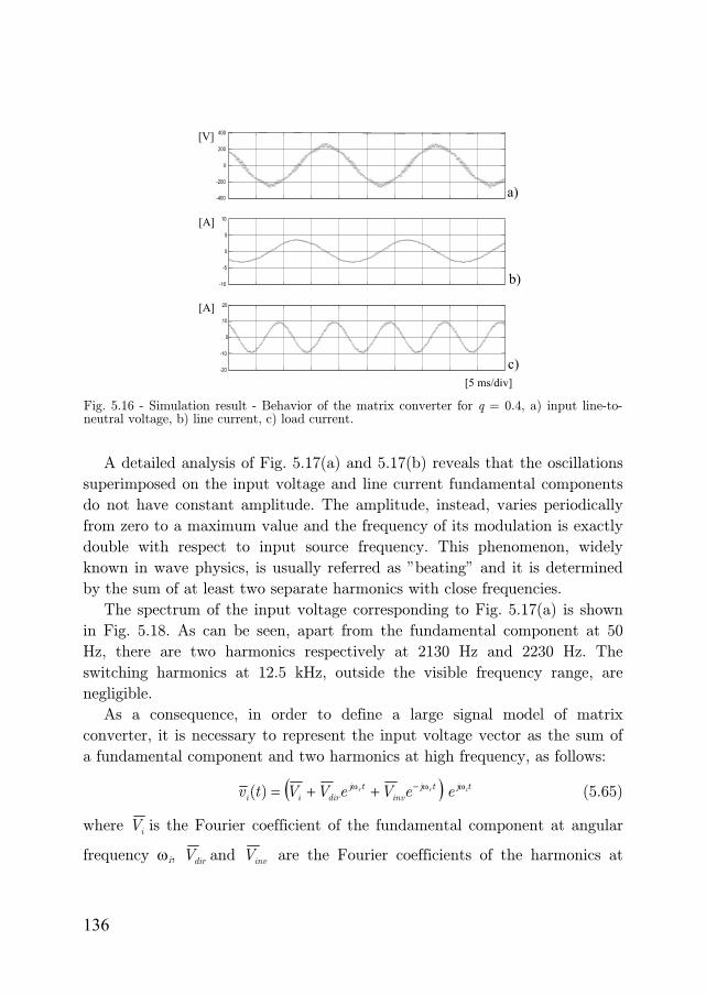
136
A detailed analysis of Fig. 5.17(a) and 5.17(b) reveals that the oscillations
superimposed on the input voltage and line current fundamental components
do not have constant amplitude. The amplitude, instead, varies periodically
from zero to a maximum value and the frequency of its modulation is exactly
double with respect to input source frequency. This phenomenon, widely
known in wave physics, is usually referred as ”beating” and it is determined
by the sum of at least two separate harmonics with close frequencies.
The spectrum of the input voltage corresponding to Fig. 5.17(a) is shown
in Fig. 5.18. As can be seen, apart from the fundamental component at 50
Hz, there are two harmonics respectively at 2130 Hz and 2230 Hz. The
switching harmonics at 12.5 kHz, outside the visible frequency range, are
negligible.
As a consequence, in order to define a large signal model of matrix
converter, it is necessary to represent the input voltage vector as the sum of
a fundamental component and two harmonics at high frequency, as follows:
( ) tjtjinv
tjdirii
irr eeVeVVtv ωω−ω ++=)( (5.65)
where iV is the Fourier coefficient of the fundamental component at angular
frequency ωi, dirV and invV are the Fourier coefficients of the harmonics at
a)
b)
c)
[V]
[A]
[A]
[5 ms/div]
-10
-5
0
5
10
-20
-10
0
10
20
-400
-200
0
200
400
Fig. 5.16 - Simulation result - Behavior of the matrix converter for q = 0.4, a) input line-to-neutral voltage, b) line current, c) load current.

137
angular frequencies ωi+ωr and ωi-ωr. The frequency ωr, that the numerical
simulations demonstrate to be close to the resonance angular frequency of the
input L-C filter, is unknown and has to be determined.
When the system is stable, obviously dirV and invV are zero. However,
voltage source perturbations or random noise, acting as excitation sources,
could force dirV and invV to assume values different from zero for a while. If
the system behaviour is stable, as soon as the temporary excitation
disappears, the system returns to the original operating conditions after a
-20
-10
0
10
20
-10
-5
0
5
10
b)
c)
[V]
[A]
[A]
[5 ms/div]
-400
-200
0
200
400
a)
Fig. 5.17 - Simulation results - Behavior of the matrix converter for q = 0.5, a) input line-to-neutral voltage, b) line current, c) load current.
0
20
40
60
80
100
120
140
160
0 500 1000 1500 2000 2500 3000 3500 4000 4500 5000
Fig. 5.18 - Simulation results - Spectrum of the input line-to-neutral voltage for q = 0.5.

138
short transient. Otherwise, if the voltage transfer ratio is greater than a limit
value, as in the case shown in Fig. 5.17, the system present steady-state
oscillations with finite-amplitude superimposed on the input voltages and
currents.
B. Expression of the Input Current
In order to find the power stability limit, it is necessary to determine the
effects on the input current produced by the distorted voltage (5.65). The
input current is completely defined once the output power waveform is
assigned. In this paragraph the output power is assumed constant, i.e.
ido Ptp =)( (5.66)
where Pid is the reference value for the power delivered to the load. Fig. 5.19
shows the block diagram of the system with constant output power.
In Appendix F it is shown that the input current can be approximated by
means of the following harmonics:
( ) tjtjinv
tjdirii
irr eeIeIIsi ωω−ω ++=)( (5.67)
where
δ
= i
i
idi
V
V
PI
23
2 (5.68)
⎟⎠⎞
⎜⎝⎛
δ−=
11
3
12 dir
dir
iddir V
V
PI (5.69)
⎟⎠⎞
⎜⎝⎛
δ−=
11
3
12 inv
inv
idinv V
V
PI . (5.70)
+*3
2
i
id
vP
)(ωZ
eqviv ii
-
Fig. 5.19 - Block diagram of the system with constant output power.

139
In (5.69)-(5.70) δ is defined as
*
241 ⎟⎟
⎠
⎞⎜⎜⎝
⎛−=δ
i
invdir
V
VV. (5.71)
There are in general two solutions for the root square of a complex
number. Therefore, it is important to note that (5.71) must be intended as
the solution in the right half of the complex plane (i.e. with positive real
part).
In (5.67) high order harmonics due to switching effects have been ignored,
because the input L-C filter acts as a low pass filter.
C. Determination of the Oscillation Magnitudes
In order to determine the magnitudes of the current and voltage
oscillations, (5.1) can be written for the specific cases ω = ωi, ω = ωi + ωr, ω
= ωi - ωr, as emphasized in (5.65) and (5.67), leading to the following system
of equations:
iiiieq VIZv +ω=ω )()( (5.72)
dirdirri VIZ +ω+ω= )(0 (5.73)
invinvri VIZ +ω−ω= )(0 . (5.74)
The system of equations (5.72)-(5.73) together with (5.68)-(5.70)
completely describe the behaviour of the system composed of the matrix
converter, the grid and the input L-C filter, either for stable or unstable
operating conditions.
5.12. Stability Analysis
The stability analysis involves the determination of solutions of the system
of equations (5.72)-(5.74). To simplify the problem, the magnitude of iV can
be considered known and close to that of the source voltage. In such a way,
only (5.73) and (5.74) are necessary to determine dirV , invV and ωr.
Substituting (5.69)-(5.70) in (5.73)-(5.74) and solving for dirV and invV

140
leads to the following explicit form for the equations of the system:
011
13
)(2
=⎥⎦
⎤⎢⎣
⎡+⎟
⎠⎞
⎜⎝⎛
δ−ω+ω dir
dir
idri V
V
PZ (5.75)
011
13
)(2
=⎥⎦
⎤⎢⎣
⎡+⎟
⎠⎞
⎜⎝⎛
δ−ω−ω inv
inv
idri V
V
PZ (5.76)
As can be seen, (5.75)-(5.76) always present the trivial solution
0== invdir VV (5.77)
that corresponds to stable, steady-state operating conditions.
Non-trivial solutions for dirV and invV can be found solving the following
system of equations, which can be obtained dividing (5.75)-(5.76) by dirV and
invV , respectively:
11
13
)(2
−=⎟⎠⎞
⎜⎝⎛
δ−ω+ω
dir
idri
V
PZ (5.78)
11
13
)(2
−=⎟⎠⎞
⎜⎝⎛
δ−ω−ω
inv
idri
V
PZ . (5.79)
A. Determination of the Angular Frequency ωr
To determine ωr, (5.78) and (5.79) must be combined multiplying term
by term (5.78) and the complex conjugate of (5.79), leading to
11
13
)(
2
2 =⎟⎟⎠
⎞⎜⎜⎝
⎛δ
−ωΩinvdir
idr
VV
P (5.80)
where
)()()( *ririr ZZ ω−ωω+ω=ωΩ . (5.81)
In (5.81) only the value in the right half of the complex plane has to be
considered.
A necessary condition for (5.80) to be verified is the existence of an
angular frequency ωr0 satisfying the following constrain equation:

141
0)(arg 02 =ωΩ r (5.82)
Equation (5.82) can be written also in the equivalent following form:
0)(arg 0 =ωΩ r (5.83)
According to (5.83), for ωr = ωr0 the function )( rωΩ is a real number,
having the dimension of an impedance. It is then useful to introduce a new
equivalent resistance Rres, defined as
)( 0rresR ωΩ= . (5.84)
B. Determination of the Amplitude of the Harmonics
Dividing term by term (5.78) and (5.79) leads to the following relationship
between the magnitude of dirV and invV :
1)(
)(2
2
0
0 =ω−ωω+ω
dir
inv
ri
ri
V
V
Z
Z. (5.85)
It is worth noting that (5.85) is not sufficient to find dirV and invV in
explicit form. However, a simple method based on a graphical approach can
be used to determine dirV and invV . For this method it is useful to introduce
the new variable p , normalised product of the harmonic amplitudes, defined
as
2
i
invdir
V
VVp = . (5.86)
The magnitudes of dirV and invV can be expressed in terms of p by solving
(5.85) and (5.86) as follows
4
1
0
0
)(
)(⎟⎟⎠
⎞⎜⎜⎝
⎛ω+ωω−ω
=ri
riidir
Z
ZpVV (5.87)
4
1
0
0
)(
)(⎟⎟⎠
⎞⎜⎜⎝
⎛ω−ωω+ω
=ri
riiinv
Z
ZpVV . (5.88)

142
As a conclusion, the knowledge of p and ωr0 is sufficient to determine the
magnitude of both voltage harmonics.
In order to study the behaviour of p, it is convenient to rewrite (5.80) in
the following form:
1)( 1 =−pAG (5.89)
where
23
2
i
idres
V
PRG = (5.90)
1
*41
11
2
1)(
−
⎥⎥⎦
⎤
⎢⎢⎣
⎡
−−=
pppA . (5.91)
It is worth noting that (5.89) can be interpreted as the characteristic
equation of the closed-loop system represented by the block diagram shown
in Fig. 5.20. G represents the forward gain, A the feedback non-linear
attenuation and p has the meaning of a state variable.
It is demonstrated in Appendix G that the solutions of (5.78)-(5.79) are
represented by the values of p defined by following parametric equation:
( ) ⎥⎥⎦
⎤
⎢⎢⎣
⎡
λ+−=λ
β 21
11
4
1)(
jep (5.92)
where λ is any positive real number and β is defined by
{ } { })(arg)(arg 00 riri ZZ ω−ω=ω+ω=β . (5.93)
G
p
1pA −)(
Fig. 5.20 - Block diagram of closed loop system equivalent to (5.89).

143
For any value of λ it is possible to calculate p and the corresponding
value of )(pA . These couples of values (p, )(pA ) can be plotted on a graph
with the values of p on the real axis and the values of )(pA on the imaginary
axis. In this way )(pA can be plotted as a function of p.
The curves of )(pA show only two types of behaviour, corresponding to
cos β > 0 and cos β <0.
Fig. 5.21(a) shows the curve of )(pA for cos β > 0. As can be seen, the
diagram starts from the point A=1 at p = 0. According to (5.89) the
determination of p can be performed by intersecting )(pA with the straight
line corresponding to the gain G, proportional to the power delivered to the
load. If G is lower than 1, an intersection is possible (state p0), but this
solution is not stable. In fact, starting from the state p0, a small decrease of p
determines an increase of the attenuation, thus causing a further decrease of
p toward the stable state p = 0. On the other side, a small increase of p
determines a decrease of the attenuation, thus causing a further increment of
p.
As a consequence, if G is lower than 1, for any disturbance of small
amplitude p< p0, the attenuation function A is greater than gain G and the
disturbance tends to vanish. If G is greater than 1, the gain G is always
greater than the attenuation function A and any small disturbance is
indefinitely amplified.
Fig. 5.21(b) shows the curves of )(pA corresponding to the case cos β < 0.
A
pp0
1 G
a)
A
pp0
1G
b)
Fig. 5.21 - Curves of the attenuation A as a function of the variable p. a) cos β > 0, b) cos β < 0.

144
In this case, no intersection between the straight line corresponding to the
gain G and the curve A is possible if G < 1. Otherwise, if G > 1 the
intersection corresponding to the state p1 can be determined. It is important
to note that this solution is stable, but the converter does not work correctly,
as a value of p different from zero means that dirV and invV have finite
magnitude and the input voltage is distorted.
As a conclusion, in both cases the stability power limit corresponds to the
condition G=1 and its value is
res
ilim
R
VP
2
3 2
= . (5.94)
From a physical point of view, it is possible to describe the behaviour of
the system in this way: a disturbance of the input voltage leads to a
corresponding disturbance of the input current, that is proportional to the
output power. The input L-C resonant filter amplifies the current disturbance
and if the output power is sufficiently high, the system can reach a new
steady state condition, but with distorted voltages.
5.13. Delay of the Digital Control
In Paragraph 5.17 it has been shown that the digital controller introduces
a delay, that leads to two main consequences. The first one is that the
controller does not keep the input current in phase with the input voltage.
The second one is that the output power cannot be considered completely
constant and equal to the desired value.
A. Delay Introduced on the Input Current Vector
As known from the control theory, the effects determined by a sample &
hold process and by the delay of the digital controller can be approximately
studied inserting the following transfer function in the block diagram of the
system.
ω−ω−
⎟⎟⎠
⎞⎜⎜⎝
⎛ω
−=ω jT
jT
ejT
eD
1)( . (5.95)
In (5.95) the term inside the brackets is related to the sampling and

145
reconstruction processes, whereas the exponential term outside the brackets is
due to the delay introduced by the digital controller. The block diagram of
the system including the delay is shown in Fig. 5.22.
Comparing the block diagram of Fig. 5.19 with that of Fig. 5.22 it can be
noted that the power limit (5.94), found in the previous paragraph, is still
valid provided that )(ωZ is replaced with the following equivalent
impedance:
)()()( ωω=ω DZZeq . (5.96)
The presence of the delay modifies the impedance mainly changing its
argument. It can be verified that in a system with delays the angular
frequency ωr0 is different from that of the same system without delays and
generally corresponds to lower values of Rres. This causes an effective
improvement of the stability power limit.
B. Variation of the Output Power due to Digital Control Delay
The output voltage can be expressed in terms of the input voltage by
means of (5.3), where the duty-cycle space vector dm and im are given by
)(3 *
,
tv
eVm
im
tjrefo
d
oω
= (5.97)
)(3 *
*,
tv
eVm
im
tjrefo
i
oω−
= . (5.98)
In (5.97) and (5.98) refoV , is the reference output voltage vector with
+*3
2
im
id
vP
)(ωZ
eqviv ii
-)(ωD imv
Fig. 5.22 - Block diagram of the system including the delay introduced by the digital controller.

146
angular frequency ωo and )(tvim is the input voltage measured by the digital
controller and used to calculate the duty-cycles.
Substituting (5.97) and (5.98) in (5.3) leads to the following expression for
the output voltage:
⎭⎬⎫
⎩⎨⎧
= ω
)(
)(Re)( ,
tv
tveVtv
im
itjrefoo
o . (5.99)
If the effects of the delay are negligible, the measured voltage coincides
with the actual voltage, namely
)()( tvtv iim = (5.100)
and (5.41) becomes:
tjrefoo
oeVtv ω= ,)( . (5.101)
Due to the delay, the measured voltage imv is slightly different from the
actual voltage iv . The explicit expression of the measured voltage can be
found multiplying (5.65) by the transfer function )(ωD . In the time domain
one finds
[ ] tjtjriinv
tjridiriim
irr eeDVeDVVtv ωω−ω ω−ω+ω+ω+= )()()( . (5.102)
Due to the inductive load, the output current is not sensitive to the
output voltage harmonics at high frequency and can be expressed as follows:
tjrefooo
oeVYti ωω= ,)()( (5.103)
where )(ωY is the admittance of the load.
Therefore, the output power can be expressed as
⎭⎬⎫
⎩⎨⎧
=⋅=)(
)(Re)()(
2
3
tv
tvPtitvp
im
iidooo (5.104)
where Pid is the output power corresponding to the reference voltage, defined
as
147
{ } 2,)(Re
2
3refooid VYP ω= . (5.105)
The analysis presented in Paragraphs 5.23 and 5.24 should be now
repeated assuming for po the expression (5.104) instead of (5.66) and taking
(5.102) into account. For doing this, the mathematical developments are not
simple and are not useful for the comprehension of the system behaviour.
However, with the aim to understand the changes that (5.104) determines
in the power limit, it is opportune to linearize the system equations assuming
that dirV and invV have small magnitudes.
Instead of the non-linear system of equations (5.75)-(5.76), the analysis
leads to the following system of equations, written in matrix form:
⎥⎦
⎤⎢⎣
⎡=⎥
⎦
⎤⎢⎣
⎡0
0*
inv
dir
V
VM (5.106)
where
⎥⎥⎥⎥
⎦
⎤
⎢⎢⎢⎢
⎣
⎡
ω−ω+
ω−ω
ω+ωω+ω+
=*22
**21
*
1211
)(1
)(
)()(1
mR
Zm
R
Z
mR
Zm
R
Z
res
ri
res
ri
res
ri
res
ri
M . (5.107)
The coefficients of the matrix M are defined as follows
2
)(111
riDm
ω+ω−= (5.108)
*
*
122
)(1
i
iri
V
VDm
ω−ω+−= (5.109)
*
*
212
)(1
i
iri
V
VDm
ω+ω+−= (5.110)
2
)(122
riDm
ω−ω−= (5.111)
and Rres is now re-defined in the general form

148
lim
ires
P
VR
2
2
3= . (5.112)
This equation is formally equivalent to (5.94). The system of equations
(5.107) has non-trivial solutions only if the determinant of M is zero, leading
to the following constraint equation:
0)()(2 =ω+ω+ rresrres cRbR (5.113)
where
*22
*11 )()()( mZmZb ririr ω−ω+ω+ω=ω (5.114)
[ ]*2112
*2211
* )()()( mmmmZZc ririr −ω−ωω+ω=ω . (5.115)
The equation (5.113) is of the second order and has two solutions Rres =
1Ω and Rres = 2Ω , namely
2
)(4)()()(
2
2,1rrr
r
cbb ω−ω±ω−=ωΩ . (5.116)
As Rres in (5.112) is a real positive number, a necessary condition for
(5.116) to be acceptable is the existence of an angular frequency ωr0 satisfying
the following constrain equation:
0)(arg 02,1 =ωΩ r . (5.117)
As can be noted, (5.117) is the general form of (5.83). After Rres is known,
the power limit can be determined solving (5.54) for Plim.
5.14. Improvement of the Stability Power Limit
The analysis described in the previous paragraphs gives important
information for the improvement of the stability power limit. Equation
(5.112) shows that the stability power limit is affected by the value of the
resistance Rres that depends on the grid and input filter impedance and on
the digital system delays.
Lower values of Rres, corresponding to higher power limits, can be obtained
reducing the peak of resonance of )(ωZ , i.e. adding damping resistors. The

149
use of damping resistance in parallel with the filter inductance is described in
[18] and [52]. A suitable value of this resistance allows the high frequency
current harmonics to flow through the source leading to lower oscillations of
the capacitor voltage. The damping effect and then the stability limit
increases while reducing the value of the resistance. Unfortunately, this
solution is effective for improving the MC stability but it is detrimental for
the EMI requirements. Therefore, a compromise should be found between
stability and input current quality.
Another important consideration for the improvement of the system
stability is the fact that the delay introduced by the digital controller affects
the angular frequency ωr. The same result can be achieved if the calculation
of the duty cycles is carried out by filtering the matrix converter input
voltages [24]-[25].
5.15. Experimental Results
In order to verify the proposed theoretical approach for the MC stability,
the same prototype presented in Paragraph 5.9 has been used. The matrix
converter is realized using the FM35E12KR3 IGBT module produced by
EUPEC. The control algorithm is implemented on the platform C6711, a
floating-point digital signal processor provided by Texas Instruments. The
switching frequency is 12.5 kHz, corresponding to a cycle period of 80 μs. The
converter is fed by a voltage transformer with variable voltage transfer ratio
to adjust the input voltage to a value of about 110 V rms. A L-C filter is
connected at the input side of the converter. The parameters of filter, supply
and load correspond to those reported in Tab. 5.2.
In order to perform experimental tests on the stability of a matrix
converter feeding a constant passive load, it is more appropriate to use the
output-to-input voltage transfer ratio q instead of Pid.
Combining (5.94), (5.105) and solving for q leads to the following value of
the limit voltage transfer ratio:
{ })(Re
1
ores
lim
YRq
ω= . (5.118)
Firstly, to validate the stability analysis, some experimental tests have

150
been performed to find the limit voltage transfer ratio.
Fig. 5.23 shows the behaviour of the matrix converter for q = 0.39. Fig.
5.23(a) represents the input voltage, Fig. 5.23(b) the line current and Fig.
5.23(c) the load current, respectively. It is evident that the system is stable,
and only a small ripple due to the switching operation can be seen.
In Figs. 5.24 and 5.25, the voltage transfer ratio has been increased to 0.46
and 0.49 respectively. As can be seen, the system becomes unstable, with
appreciable oscillations on both input voltage and line current.
The spectral analysis of the input voltage is given in Fig. 5.26 and shows
that there are two main harmonics with frequencies of 2150 Hz e 2250 Hz,
respectively. This result is in good agreement with the proposed theoretical
approach, as the two frequencies differ for the double of the input frequency
(2π50 Hz = 100 Hz). In addition, the amplitude of the oscillations tends to
increase with the output power as predicted by the stability analysis for the
case with cos β < 0.
In Tab. 5.3 the limit voltage transfer ratio calculated by means of the
proposed theory is compared with the experimental limit value, namely q ≅
0.45.
The basic theory, that neglects both the effects caused by the delay,
-5
0
5
-10
-5
0
5
10
-400
-200
0
200
400
a)
b)
c)
[V]
[A]
[A]
[5 ms/div]
Fig. 5.23 - Experimental tests - Behavior of the matrix converter for q = 0.39, a) input line-to-line voltage, b) line current, c) load current.
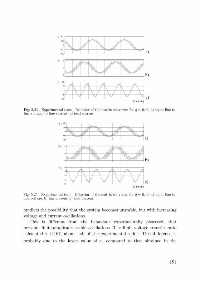
151
predicts the possibility that the system becomes unstable, but with increasing
voltage and current oscillations.
This is different from the behaviour experimentally observed, that
presents finite-amplitude stable oscillations. The limit voltage transfer ratio
calculated is 0.167, about half of the experimental value. This difference is
probably due to the lower value of ωr compared to that obtained in the
-5
0
5
-10
-5
0
5
10
-400
-200
0
200
400
a)
b)
c)
[V]
[A]
[A]
[5 ms/div]
Fig. 5.24 - Experimental tests - Behavior of the matrix converter for q = 0.46, a) input line-to-line voltage, b) line current, c) load current.
-5
0
5
-10
-5
0
5
10
-400
-200
0
200
400
a)
b)
c)
[V]
[A]
[A]
[5 ms/div]
Fig. 5.25 - Experimental tests - Behavior of the matrix converter for q = 0.49, a) input line-to-line voltage, b) line current, c) load current.

152
experimental test.
Better results can be found if the delay introduced by the digital
controller is taken into account. In this case, (5.83) presents several solutions.
Obviously, the stability power limit has to be evaluated with reference to the
worst case, corresponding to the lowest value of qlim.
If the output power is assumed constant, qlim results 0.230. However, the
second solution (i.e. qlim = 0.443, ωr/2π = 2180 Hz) presents a behaviour that
is very close to that of the actual system. This means that it is essential to
take the delay into account to describe the real system.
0 500 1000 1500 2000 2500 3000 3500 4000 4500 50000
20
40
60
80
100
120
140
160
Fig. 5.26 - Experimental tests. Spectrum of the input line-to-neutral voltageduring unstable operation of the converter.
TABLE 5.3 - COMPARISON BETWEEN THEORETICAL RESULT AND EXPERIMENTAL TESTS
Mathematical model π
ω2
r cos β Rres qlim Solution type
Basic theory (no delays and Po=Pid)
1739 0.53 299 0.167 Unstable oscillations
Model with delays, but output power is assumed constant.
1630 2180
0.98 -0.99
158,9 42,67
0.230 0.443
Unstable oscillations Stable oscillations
Model with Po=Po(t) 1616 0.39 133,0 0.251 Unstable oscillations
Complete model, with delays and Po=P(t)
1007 2182 3142
0.75 -0.99 -0.69
17.29 42.17 13,18
0.696 0.446 0.797
Unstable oscillations Stable oscillations Stable oscillations
Experimental tests 2200 - - 0.44 Stable oscillations

153
If the output power is not assumed constant and the effect of the delay on
the input current displacement is neglected, then the limit voltage ratio
increases to 0.251.
Finally, if both the effects caused by the delays of the digital controller are
considered, the theory predicts the value 0.446 for the limit voltage transfer
ratio that is just a little lower than the experimental value. In addition, the
frequency and the behaviour of the oscillations are in good agreement with
the experimental results. The small mismatching between theoretical
predictions and experimental values may be ascribed to several factors, such
as converter power losses and parameter uncertainties.
It is worth noting that this analysis does not consider the effect of the
converter losses for the sake of brevity. The power limit that can be
calculated by means of the equations presented in the previous paragraph is
generally lower than that achievable in experimental tests. This is because
the iron losses in the inductances or the power losses of the converter may
increase the damping effect of the real system, thus preventing unstable
oscillations to arise. The effect of the losses is more or less evident depending
on the operating conditions and the system parameters. In particular, the
damping effect could be very evident if the theoretical stability power limit
would be small and comparable with the converter losses.
Another case in which the damping effect of the losses becomes evident is
when the digital filter is used, and this is because the consequent power limit
increase leads to higher losses as shown in [25].
Several tests have been performed, for different values of the time
constant τ of the input voltage digital filter in order to evaluate the limit
voltage transfer ratio. The discrete-time version of the digital filter is
presented in Appendix D. The experimental results are reported in Fig. 5.27.
The dashed area between the two curves represents an uncertainty region,
where it is not possible to clearly state if the system is stable or unstable.
In fact, in experimental tests the unstable behaviour of the converter can
be established only in case of input voltage and current oscillations higher
than a threshold value. If the output power is not sufficiently greater than
the stability limit, these oscillations are very small and can be confused with
the natural disturbances due to the interaction between the switched current
and the input L-C filter.

154
The frequency of the oscillations was about 1850 Hz at τ = 0.9 ms and
moves toward higher values as τ decreases.
Additional tests were carried out considering digital filters of the 2nd and
3rd order. These filters were implemented using filters of first order in
cascade. Fig. 5.28 shows in percent the increase of the limit voltage transfer
ratio with respect to the case of first order filtering.
5.16. Conclusion
In the first part of this chapter a complete analysis of the stability of
matrix converters has been carried out using a small signal analysis around a
steady-state operating point. A complex mathematical model was necessary
100
110
120
130
140
150
160
0.5 0.55 0.6 0.65 0.7 0.75
%
Filter time constantτ [ms]
3rd order
2nd order
Fig. 5.28 - Experimental tests - Percentage of increment of the limit voltage transfer ratio for filters of 2nd and 3rd order.
0.4
0.5
0.6
0.7
0.8
0.9
0.0 0.2 0.4 0.6 0.8 1.0
Vol
tage
tran
sfer
ratio
, q
Filter time constantτ [ms]
unstable
stable
Fig. 5.27 - Experimental tests. Limit voltage transfer ratio as a function of the input digitalfilter τ.

155
to include all the system parameters and to emphasize their effect on the
matrix converter stability. Particular attention has been paid to take the
time delay introduced by digital controllers and the matrix converter power
losses into account.
In the second part of this chapter, the analysis of the stability of matrix
converters has been carried out using a large signal analysis based on the
physical observation that the instability phenomena can be described as
beatings.
The proposed analytical methods can be usefully adopted for the
estimation of the maximum output power and for choosing among different
input filter topologies. Furthermore they help understanding the operating
principle of some common methods to increase the system stability, such as
filtering the input voltages.
Finally, several experimental tests are reported to validate the theoretical
approach.

156
6.Chapter 6 Quality of the Input Current Abstract
This chapter deals with the quality of the input currents in matrix
converters under input and output unbalanced conditions. Two control
strategies of the input current displacement angle are presented and
compared in order to emphasise their influence on the input current
harmonic content. The first one is based on keeping the input current vector
in phase with the input voltage vector. In the second one the input current
displacement angle is dynamically modulated as function of positive and
negative sequence components of the input voltages. In both cases the
harmonic content and the three-phase RMS value of the input current have
been evaluated analytically. In the second part of the chapter a general
approach for the determination of the line current harmonic content in
matrix converters is presented. The input disturbances, such as voltage
unbalance and voltage harmonics, are considered as perturbations of the
fundamental component, and a small-signal analysis is used to determine the
spectrum of the line current. The proposed analytical approach has a general
validity, because it takes the effects of the line and filter impedance into
account, and can be usefully employed to evaluate the line current quality in

157
the point of common coupling for different filter topologies and supply
distortions. Experimental results are given to confirm the analytical solution.
6.1. Introduction
As the matrix converter has no DC-link energy storage, any disturbance in
the input voltages will be reflected in the output voltages. In particular,
considering unbalanced input voltages, most of the modulation strategies
introduce low order harmonics in the output voltages. The effects of
unbalanced supply voltages have been already investigated in traditional
converters [57]-[59], and recently some attention has been paid also to matrix
converter [60]-[62].
In [61] a SVM algorithm for matrix converters has been presented which
allows balanced output voltages to be generated, even under unbalanced
supply conditions. As known, in the case of unbalanced supply voltages, the
negative sequence components of the voltage system causes variation in
magnitude and angular velocity of the input voltage vector. As a
consequence, a simple synchronisation with the input voltages, as under
balanced conditions, is no longer applicable and the input voltages have to be
measured at each sampling instant. Owing to the angular velocity variation
of the input voltage vector some problems arise in defining the input current
displacement angle. In [61] the input current vector has been modulated in
order to be, at any instant, in phase with the input voltage vector. In [62] the
matrix converter analysis has been developed in order to take account of both
input and output unbalance.
In the first part of this chapter an input current modulation strategy is
proposed in order to reduce the harmonic content of the input current under
unbalanced conditions and is compared to that described in [61]. The
proposed control strategy is based on a dynamic modulation of the
instantaneous displacement angle between input voltage and current vectors.
The modulation law is determined as function of the magnitude and phase
angle of positive and negative sequence components of the input voltages.
The corresponding harmonic content, as well as the three-phase RMS value
of the input current, has been determined analytically in the general case of
input and output voltage unbalance.
A numerical simulation of the matrix converter has been carried out

158
assuming ideal switching devices. Some numerical results are presented in
order to show the influence of input and output unbalance on the input
current RMS value and input current harmonic content.
6.2. Input And Output Unbalance Representation
The input current of the matrix converter can be expressed as a function
of the output power and the input voltage, as follows:
ψ+ψ
ψ= ∗∗ e e
p i
ii
oi
3
4. (6.1)
Equation (6.1) is a general expression of the input current vector which
can be further developed for any particular case. In the following the analysis
will be focused on the development of (6.1) under input and output
unbalanced conditions. In particular, for unbalanced supply voltages and
sinusoidal conditions with period Ti=2π/ωi , the input line-to-neutral voltage
vector can be written as
*inip
t j in
t jipi eee EeEe ii +=+= ω−∗ω (6.2)
where ipE and inE are the time phasors of positive and negative symmetrical
components of the line-to-neutral input voltages. It should be noted that,
when a voltage unbalance is present, the negative sequence component causes
the input voltage vector trajectory to change from circular to elliptical shape.
This causes variations in input voltage vector magnitude and angular
velocity.
By substituting (6.2) in (6.1) yields
( ) ( ) ψψ++ψ+
= ∗ω−∗ωωω− eEeE eEeE
pi
t j in
t jip
t j in
t j*ip
o
iiiii
3
4
. (6.3)
In order to make an analysis concerning balanced and unbalanced output
conditions the effects due to the switching harmonics are neglected.
Considering balanced output conditions the output power assumes a constant
value. On the contrary, under unbalanced output conditions the output
power can be in general expressed as the sum of a constant and an

159
alternating component. In this case the analysis requires the output
quantities also to be expressed in terms of symmetrical components, as
follows:
t j on
t jopo
oo eEeEe ω−∗ω += (6.4)
t j on
t jopo
oo eIeIi ω−∗ω += . (6.5)
Substituting (6.4) and (6.5) in (6.3) leads to the following expression for
the input current vector:
( ) ( ) ψψ++ψ+
++= ∗ω−∗ωωω−
ω−∗ω
eEeE eEeE
eCe CCi
t j in
t jip
t j in
t j*ip
t j t j
iiiii
oo 22
221 (6.6)
where the constants C1 and 2C are given by
opononop
ononopopononopop
IEIEC
I E I E I E I E C
+=
+++= ∗∗∗∗
2
1 (6.7)
It can be shown that the constants C1 and 2C are related to the mean
value Pom and to the alternating component Poa of the output power
respectively, by the following relationships
omP C3
41 = , oaP C
3
22 = . (6.8)
Equations (6.3) and (6.6) show that the input current vector is influenced
by the choice of the space vector ψ along which the input current is
modulated. The choice of this space vector is important because it determines
the input current harmonic content. The difference between the two
modulation strategies described below is concerned with the choice of the
space vector ψ .
6.3. Constant Displacement Angle Between Input Voltage And Current Vectors (Method 1)
As explained above, with unbalanced supply voltage, the input voltage
vector has variable angular velocity. Then, a possible modulation strategy

160
can be adopted in order to keep, at any instant, a constant displacement
angle between input voltage and current vectors. In this case the input
current vector direction can be defined by
( ) ( ) iiiii j inip
j t j in
t jip
j i eeee eEe E=e e ϕ−ϕ−ω−∗ωϕ− +=+=ψ * (6.9)
Fig. 6.1 shows the corresponding space vector representation in the d-q
plane.
Introducing (6.9) in (6.6), after some manipulations leads to
( )t jin
t j ip
t j t j
i
j
iii
ooi
eEeE
eCeC+Cei ωω−∗
ω−∗ωϕ−
++
ϕ=
22
221
cos2 (6.10)
Equation (6.10) clearly emphasises the influence of the input current
displacement angle iϕ . Of course, assuming iϕ =0 leads to the lowest value
for the input current vector magnitude.
In order to evaluate the input current quality it is necessary to determine
the harmonic content of the input current vector. For this purpose it is
opportune to express by complex Fourier series the following term of (6.10)
( ) ∑∑∞
=
ω−∗∞
=
ωωω−∗ + 10
1
k
t k j nk
k
t k jpkt j
int j
ip
ii
iie A + e A =
e E e E (6.11)
Rearranging (6.11) and equating terms with the same angular frequency it
is possible to show that all even harmonic symmetrical components of the
input current are identically null. The odd harmonic symmetrical components
eipeeein
ei
*
βi
q-axis
d-axis
ϕi
i i
ψ=const.
Fig. 6.1 - Space vector representation of Method 1.
161
for inip E E > are as follows:
,...3,11 2
1
k E
E
EA
k
ip
in
ip
pk =⎟⎟⎠
⎞⎜⎜⎝
⎛−=
−
∗∗ (6.12)
,...3,10 k Ank == (6.13)
Taking the results obtained into account, (6.10) gives the input current
vector in terms of complex Fourier series which can be expressed as
( )
( )
⎥⎥⎥
⎦
⎤
⎟⎟⎠
⎞⎜⎜⎝
⎛−+
+⎟⎟⎠
⎞⎜⎜⎝
⎛−+
⎢⎢⎢
⎣
⎡
⎟⎟⎠
⎞⎜⎜⎝
⎛−
ϕ=
∑
∑∑
∞
=
ω+ω−
−
∗∗
∗
∞
=
ω+ω
−
∗∗
∞
=
ω
−
∗∗
ϕ−
3,1
22
1
2
3,1
22
1
2
3,1
2
1
1
cos2
k
t kj
k
ip
in
ip
k
t k j
k
ip
in
ip k
tjk
k
ip
in
ipi
j
i
io
ioi
i
eE
E
E
C
eE
E
E
C e
E
E
E
Cei
(6.14)
As (6.14) shows, the harmonic content of ii is represented by three series
of harmonics which decay by the input unbalance degree u, which is defined
as
ipin EEu = . (6.15)
The displacement angle iϕ has the same influence on all the current
harmonic components. The magnitude of the harmonic components are
related to the output power by means of the constants C1 and 2C . In
particular the first series depends on the average value of the output power,
while the second and third series depend on the amplitude of the output
power alternating component. It should be noted that the third series may
introduce sub-harmonic components depending on the difference between
input and output frequency.
The harmonic content of the three line currents can be derived from the
harmonic content of the input current vector.
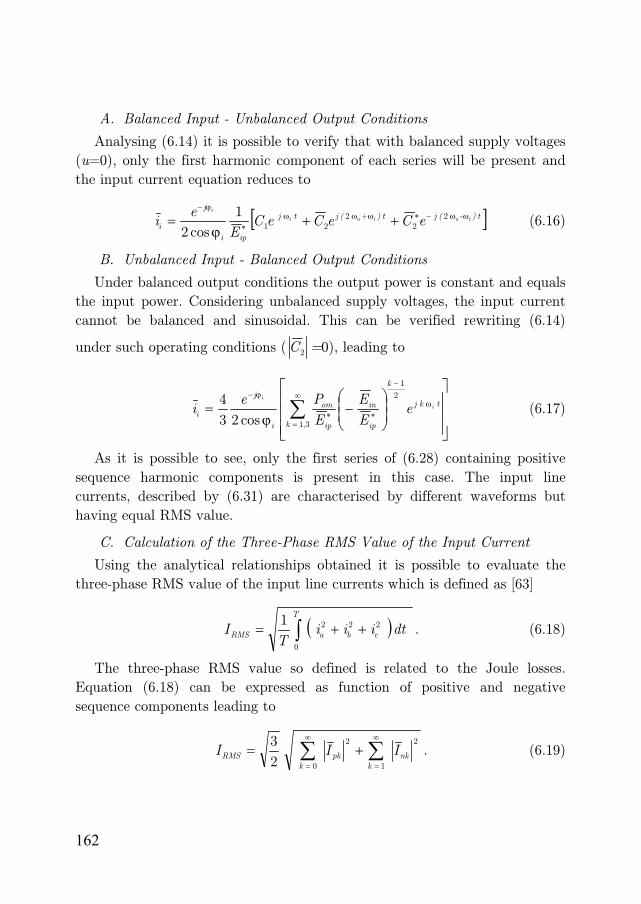
162
A. Balanced Input - Unbalanced Output Conditions
Analysing (6.14) it is possible to verify that with balanced supply voltages
(u=0), only the first harmonic component of each series will be present and
the input current equation reduces to
[ ]t )- ( j t )+ ( jt j
ipi
j
iioioi
i
eCeCeCE
ei ωω−∗ωωω
∗
ϕ−
++ϕ
= 22
221
1
cos2 (6.16)
B. Unbalanced Input - Balanced Output Conditions
Under balanced output conditions the output power is constant and equals
the input power. Considering unbalanced supply voltages, the input current
cannot be balanced and sinusoidal. This can be verified rewriting (6.14)
under such operating conditions ( 2C =0), leading to
⎥⎥⎥
⎦
⎤
⎢⎢⎢
⎣
⎡
⎟⎟⎠
⎞⎜⎜⎝
⎛−
ϕ= ∑
∞
=
ω
−
∗∗
ϕ−
3,1
2
1
cos23
4
k
t k j
k
ip
in
ip
om
i
j
ii
i
eE
E
E
Pei (6.17)
As it is possible to see, only the first series of (6.28) containing positive
sequence harmonic components is present in this case. The input line
currents, described by (6.31) are characterised by different waveforms but
having equal RMS value.
C. Calculation of the Three-Phase RMS Value of the Input Current
Using the analytical relationships obtained it is possible to evaluate the
three-phase RMS value of the input line currents which is defined as [63]
( ) dt i i i T
IT
cbaRMS ∫ ++=0
2221. (6.18)
The three-phase RMS value so defined is related to the Joule losses.
Equation (6.18) can be expressed as function of positive and negative
sequence components leading to
∑∑∞
=
∞
=
+=1
2
0
2
2
3
knk
kpkRMS I I I . (6.19)

163
Equation (6.19) is a general expression and can be further developed
taking the results of (6.14) into account. If all the harmonic components in
(6.14) have different harmonic order, (6.19) becomes
P
P+
u E
P I
iom
oa
ip
omRMS ϕ−
=cos
1
2
11
1
1
3
22
2
2 (6.20)
The previous equation shows how the three-phase RMS value is affected
by the input current displacement angle, the input unbalance degree and the
output unbalance defined by the ratio between the alternating component
and the mean value of the output power. From (6.20) it is possible to derive
the three-phase RMS value of the input current vector for unity input power
factor (ϕi=0), balanced supply voltages (u=0) and balanced output voltages
(Poa=0).
Equation (6.20) shows that operating the matrix converter with ϕi=0
leads to the lowest three-phase RMS value of the input current vector. It
could be shown that this result is valid also considering any modulation
strategy of ϕi.
6.4. Variable Displacement Angle Between Input Voltage And Current Vectors (Method 2)
As explained above, the harmonic content of the input current is strongly
influenced by the choice of the input current reference angle. Analysing (6.20)
we can note that a reduction of the harmonic content could be achieved
applying a new modulation strategy of the input current displacement angle
defined by the following expression
*inip
t j in
t jip eee E e E ii −=−=ψ ω−∗ω (6.21)
The space vector representation of this input current modulation is given
in Fig. 6.2. As it is possible to see, due to the opposite angular velocity of ipe
and *ine , a dynamic modulation of the input current displacement angle is
obtained.
The implementation of the modulation law expressed by (6.21) is more
complex with respect to that given by (6.9) being related to the positive and
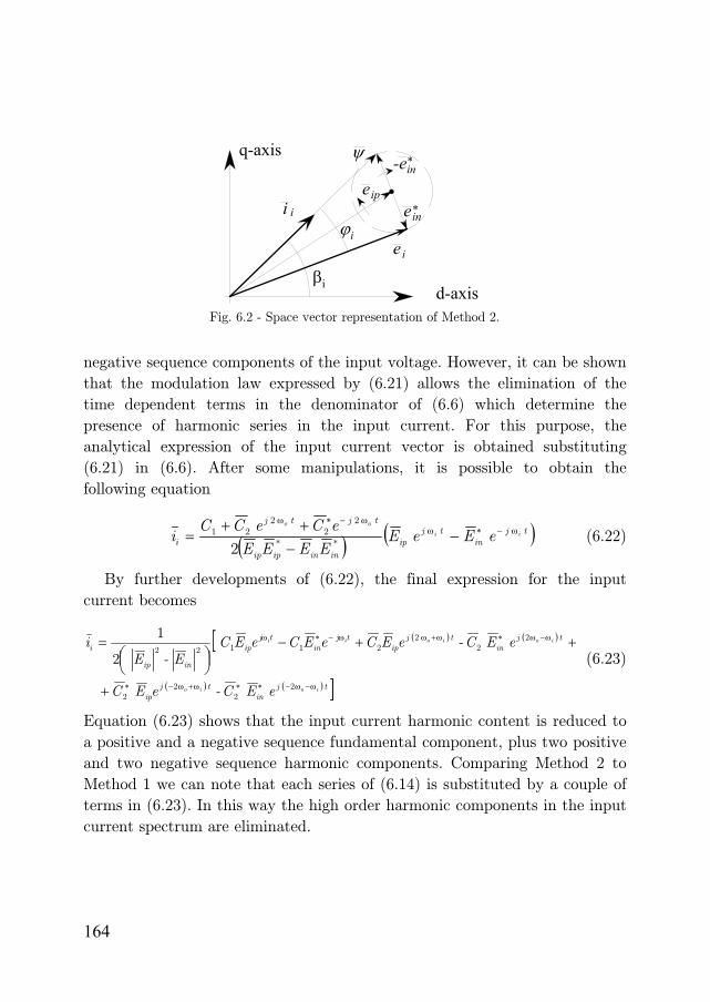
164
negative sequence components of the input voltage. However, it can be shown
that the modulation law expressed by (6.21) allows the elimination of the
time dependent terms in the denominator of (6.6) which determine the
presence of harmonic series in the input current. For this purpose, the
analytical expression of the input current vector is obtained substituting
(6.21) in (6.6). After some manipulations, it is possible to obtain the
following equation
( ) ( ) e E e E EEEE
eCe CCi t j
int j
ip
ininipip
t j t j
iii
ooω−∗ω
ω−∗ω
−−
++=
**
22
221
2 (6.22)
By further developments of (6.22), the final expression for the input
current becomes
[ ( ) ( )
( ) ( ) ] e E C-eE C
e E C-eECeECeEC E-E
i
t jin
t jip
t jin
t jip
tj in
tjip
inip
i
ioio
ioioii
ω−ω−∗∗ω+ω−∗
ω−ω∗ω+ωω−∗ω
+
++−⎟⎠⎞⎜
⎝⎛
=
22
22
22
221122
2
1
(6.23)
Equation (6.23) shows that the input current harmonic content is reduced to
a positive and a negative sequence fundamental component, plus two positive
and two negative sequence harmonic components. Comparing Method 2 to
Method 1 we can note that each series of (6.14) is substituted by a couple of
terms in (6.23). In this way the high order harmonic components in the input
current spectrum are eliminated.
eip
ei
ein*
βi
q-axis
d-axis
-ein*
i iϕi
ψ
Fig. 6.2 - Space vector representation of Method 2.

165
A. Balanced Input - Unbalanced Output Conditions
In this case the equation of the input current vector can be obtained
rewriting (6.23) with Ein=0, leading to
[ ( ) ( ) ]t jt jtj
ip
iioioi e C eCeC
Ei ω+ω−∗ω+ωω ++= 2
22
21*2
1 (6.24)
By comparing (6.24) to (6.16) it appears that Method 2 is equivalent to
Method 1 when operated with ϕi=0.
B. Unbalanced Input - Balanced Output Conditions
The use of Method 2 is particularly effective in the usual case of balanced
output conditions ( 2C =0). In fact in this case (6.23) reduces to
[ ]t j in
t jip
inip
omi
ii eEeE E-E
Pi ω−∗ω −
⎟⎠⎞⎜
⎝⎛
=223
2 (6.25)
As it is possible to see the current spectrum contains only the positive and
the negative sequence fundamental component, so determining unbalanced
but sinusoidal input line currents.
By comparing (6.25) to (6.17) the improvement achieved in the harmonic
content of the input current using Method 2 is particularly evident.
C. Calculation of Input Current RMS Value
If all the harmonic components in (6.23) have different harmonic order,
the three-phase RMS value of the input current becomes
2
2
2
2
2
11
1
1
3
2
om
oa
ip
omRMS
P
P
u
u
E
P I +
−+
= (6.26)
Equation (6.26) shows how the three-phase RMS value is affected by the
input unbalance degree and the output unbalance.
6.5. Numerical Simulations
Two different simulation models for the matrix converter have been used
in the analysis. The first is based on the power balance equation, neglecting

166
the losses and switching effects of the converter.
In order to apply this model it is necessary to calculate the input voltage
vector ie for a given set of input voltages. Then, the input current vector ii
can be determined by (6.1) for a given output power Po once the reference
displacement angle of the input current is known. Finally the input line
currents are readily evaluated and the harmonic content of ii can be
determined by numerical integration. The three-phase RMS value is
calculated by (6.19).
For the numerical examples the following supply unbalance has been
considered
ipE = 300 V / 0° , inE =30 V / 0°
The input frequency is fi = 50 Hz and the output frequency is fo = 80 Hz.
6.6. Unbalanced Output Conditions
In the case of unbalanced output conditions the output voltages and
currents have been assumed as follows
opE = 300/√3 V / -30° onE = 0
opI = 208 A / -67° onI = 41.5 A / -67°
Fig. 6.3 shows the harmonic content of the input current vector when
Method 1 is applied with unity input power factor (ϕi=0). As predicted by
(6.14), three series of harmonics have been obtained. In Fig. 6.3, the three
series are clearly denoted by different symbols. The first harmonic
components of the series have frequency of -110 Hz, 50 Hz and 210 Hz. Note
that negative values of frequency represent negative sequence harmonic
components.
Fig. 6.4 shows the harmonic content of the input current vector when
Method 2 is employed. Analysing Figs. 6.3 and 6.4 it appears that the new
modulation strategy performs in order to transform each series of harmonics
of Method 1, into a positive and a negative sequence component, having the
same frequency of the first harmonics. The amplitudes and the frequencies of
these harmonic components are in full agreement with that predicted by

167
(6.23).
The three-phase RMS value of the input currents is 120 A for Method 1
and 121 A for Method 2. The same values have been obtained using (6.20)
and (6.26) respectively. It can be noted that the reduction of the input
current harmonic content has been obtained without appreciable increase of
the input current three-phase RMS value.
6.7. Balanced Output Conditions
In order to emphasise the effectiveness of Method 2 an example with
balanced output conditions has been investigated. The output voltages and
currents have been assumed as follows
Fig. 6.3 - Input current spectrum, Method 1.
Fig. 6.4 - Input current spectrum, Method 2.

168
opE = 300/√3 V / -30° onE = 0
opI = 208 A / -67° onI =0
Fig. 6.5 represents the input current spectrum using Method 1. In this
figure it is possible to note the presence of a series of positive sequence
harmonic components, as predicted by (6.17).
Fig. 6.6 represents the harmonic content obtained using Method 2. In this
case the new modulation strategy determines sinusoidal input currents
characterised by only a positive and a negative fundamental component, as it
appears in (6.25). The three-phase RMS value of the input currents is 118 A
for Method 1 and 119 A for Method 2.
Taking into account that Method 1 gives the lowest three-phase RMS
Fig. 6.5- Input current spectrum, Method 1.
Fig. 6.6 - Input current spectrum, Method 2.
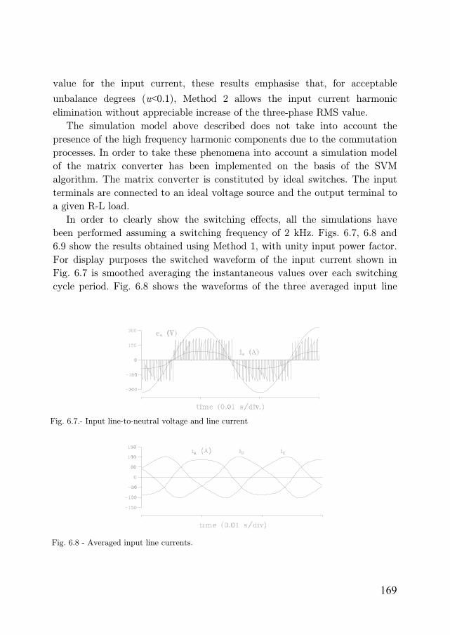
169
value for the input current, these results emphasise that, for acceptable
unbalance degrees (u<0.1), Method 2 allows the input current harmonic
elimination without appreciable increase of the three-phase RMS value.
The simulation model above described does not take into account the
presence of the high frequency harmonic components due to the commutation
processes. In order to take these phenomena into account a simulation model
of the matrix converter has been implemented on the basis of the SVM
algorithm. The matrix converter is constituted by ideal switches. The input
terminals are connected to an ideal voltage source and the output terminal to
a given R-L load.
In order to clearly show the switching effects, all the simulations have
been performed assuming a switching frequency of 2 kHz. Figs. 6.7, 6.8 and
6.9 show the results obtained using Method 1, with unity input power factor.
For display purposes the switched waveform of the input current shown in
Fig. 6.7 is smoothed averaging the instantaneous values over each switching
cycle period. Fig. 6.8 shows the waveforms of the three averaged input line
Fig. 6.7.- Input line-to-neutral voltage and line current
Fig. 6.8 - Averaged input line currents.

170
currents. It is possible to verify that the input line currents have the same
RMS value even if they show different waveforms. Fig. 6.9 shows the
harmonic content of the switched input currents. As it is possible to see, the
higher amplitude harmonics correspond to those given in Fig. 6.5. The lower
amplitude harmonics shown in Fig. 6.5 are, in Fig. 6.9, obscured by the
switching harmonics. Figs. 6.10, 6.11 and 6.12 show the numerical results obtained using
Method 2, for the same operating conditions used for Method 1. Comparing
Figs. 6.8 and 6.11 to Figs. 6.9 and 6.12 respectively it is evident the effect
produced by the new modulation strategy which determines sinusoidal input
currents, as predicted by (6.25). The presence of the negative sequence
fundamental components determines different amplitude for the three input
line currents. Fig. 6.12 shows the harmonic content of the switched input
Fig. 6.9 - Input current spectrum.
Fig. 6.10 - Input line-to-neutral voltage and line current.

171
currents. In this case also the higher amplitude harmonics match against the
corresponding harmonics given in Fig. 6.6.
6.8. Preliminary Conclusions
Two input current modulation strategies for matrix converters have been
analysed. The first one (Method 1) operates in order to keep the input
current vector in phase with the input voltage vector. This strategy can be
easily implemented requiring only the determination of the phase angle of the
input voltage vector. Furthermore, it determines input currents with the
lowest three-phase RMS value.
The second strategy (Method 2) is some more complicated to be
implemented but it has the advantage concerning the possibility to reduce or
eliminate the harmonic content of the input current. It has been shown that
the improvement of the input current quality can be achieved without
appreciable increase of the three-phase RMS value given by Method 1.
Fig. 6.11 - Averaged input line currents.
Fig. 6.12 - Input current spectrum.

172
The two input current modulation strategies have been implemented using
a SVM algorithm which ensures sinusoidal and balanced output voltages even
under unbalanced input voltages.
For both strategies the input current harmonic spectrum and the three-
phase RMS value have been determined analytically showing the influence of
input and output unbalance conditions.
The validity of the theoretical analysis and the performance of the
modulation algorithm have been confirmed by numerical simulations.
6.9. Introduction to the General Analysis of the Input Current
In the previous paragraphs two modulation strategies of the input current
reference angle have been proposed in order to reduce the harmonic content
of the input current under unbalanced supply voltages.
However, the supply voltages not only are usually unbalanced to some
extent, but also show a typical distortion due to the presence of nonlinear
loads connected to the grid. Hence, it is of practical interest to investigate
the performance of MCs in these operating conditions as well [64], [65].
A general analysis on the input current for unbalanced and distorted input
voltages was presented in [22].
Recently, industry has paid particular attention to this problem, that is
important for EM compatibility and line current quality. In [66] the attention
is focused on the input and output filters to meet the restrictive CISPR 11
standards, whereas an active damping has been proposed in [67] to reduce the
line harmonics.
In the second part of this chapter, a general approach is developed in
order to predict the spectrum of the line current of MCs controlled with the
Space-Vector Modulation (SVM) technique in the case of unbalanced and
non-sinusoidal supply voltages. The input current harmonic content is
obtained with a small signal analysis of the system equations. In this way, it
is possible to investigate the converter performance under any condition
determined by input disturbances. The main advantage of the proposed
approach is the possibility to consider the effects of the line and filter
impedance, that can be important for detecting the resonant behaviours of
the converter. The results of the analysis could be of considerable interest in

173
the design of the input filters.
6.10. Basic Equations
The system considered for the analysis is composed of a power supply, a
second order input L-C filter, and a MC feeding a passive load. The system is
the same shown in Fig. 5.1, where space vector notation is used for the
representation of the system variables.
The input filter is generally needed to smooth the input currents and to
satisfy the EMI requirements. It is also known that the design of the input
filters is strictly related to the switching frequency [68]. If the input filter is
well designed, current harmonics at frequencies greater or equal to the
switching frequency are smoothed adequately.
In this paragraph the main equations related to the system represented in
Fig. 5.1 will be introduced. The variables t and ω will be used to distinguish
between the time domain and the Fourier domain respectively.
In the following, the analytical developments are carried out neglecting
the effects of the switching harmonics, considering for the output voltages
and input currents their average values over a cycle period Tp.
The input current modulation strategy keeps the input current vector in
phase with the actual input voltage vector, determining instantaneous unity
input power factor.
However, as shown in the beginning of this chapter, variants of this
modulation strategies are possible to reject the input voltage disturbances,
such as the one based on keeping the input current vector in phase with the
fundamental component of input voltage vector instead of its instantaneous
value [22].
Hence, it is convenient to consider the modulation vector as a function of
the input voltage vector, and eventually of its derivatives and integrals, as
follows:
),,( dtvdt
vdv ∫ψ=ψ . (6.27)
The equation for the input side of the MC, written in the Fourier domain,
is as follows:

174
)()()()( ω+ωω=ω viZEeq (6.28)
where )(ωeqE and )(ωZ are the Thevenin equivalent voltage and impedance
of the voltage source and input filter.
For the particular case shown in Fig. 5.1, )(ωeqE and )(ωZ can be
expressed as functions of the line and filter parameters as follows:
)(1
)()(
ωω+ω
=ωtotf
seq
ZCj
eE (6.29)
)(1
)()(
ωω+ω
=ωtotf
tot
ZCj
ZZ (6.30)
where
ff
ff
sstotRLj
RLjLjRZ
+ωω
+ω+=ω)( . (6.31)
The behaviour of the system at the input side is completely described by
(1.4) and (6.28) once the converter power and the modulation law are
assigned.
The line current, instead, depends on the filter topology. For the typical
case shown in Fig. 5.1, the line current is
)(
)()()(ω
ω−ω=ω
tot
sL Z
vei . (6.32)
As can be seen from (6.32), to determine the line current spectrum, it is
necessary to know the spectrum of the input voltage vector. However, the
input voltage depends on the current absorbed by the converter, due to the
voltage drop on the impedance of the line and the filter.
For this reason, to determine the line current spectrum, it is necessary to
solve the set of non-linear equations (1.4), (6.27) and (6.28). The solution of
this problem will be presented in the following sub-sections.
A. Steady State Operating Conditions with Balanced and Sinusoidal Supply Voltages
In steady-state operating conditions, with balanced and sinusoidal supply
175
voltages, the input voltages can be represented by means of rotating space
vectors with constant magnitudes as follows:
tjeq
ieEtE ω= 1)( (6.33)
tj ieVtv ω= 1)( (6.34)
where ωi is the angular frequency of the voltage source.
In these operating conditions, the modulation vector coincides with the
input voltage vector, as follows:
tj ieVt ω=ψ 1)( . (6.35)
B. Steady State Operating Conditions with Unbalanced and Non-sinusoidal Supply Voltages.
If the supply voltages are not balanced and sinusoidal, then (6.33)-(6.35)
must be rewritten in the following form:
)()( 1 tEeEtE eqtj
eqi Δ+= ω (6.36)
)()( 1 tveVtv tj i Δ+= ω (6.37)
)()( 1 teVt tj i ψΔ+=ψ ω (6.38)
where )(tEeqΔ , )(tvΔ and )(tψΔ are the perturbations of each quantity with
respect to its fundamental harmonic.
It is convenient to rewrite (6.37) and (6.38) in terms of new variables, that
allow one to make easier the mathematical approach, as follows:
( ))(1)( 1 teVtv tj i ε+= ω (6.39)
( ))(1)( 1 teVt tj i γ+=ψ ω (6.40)
where
tj ieV
tvt ω−Δ
=ε1
)()( (6.41)
tj ieV
tt ω−ψΔ
=γ1
)()( . (6.42)

176
As can be seen from (6.41) and (6.42), )(tε and )(tγ represent the
perturbations )(tvΔ and )(tψΔ written in p.u. in a reference frame
synchronous with the fundamental component of the input voltage.
The expression of the input current can be found under the assumption
that the perturbations )(tvΔ and )(tψΔ are small compared to the
fundamental harmonics. Substituting (6.39) and (6.40) in (1.4) leads to the
following expression of the input current, valid for small signals:
⎟⎟⎠
⎞⎜⎜⎝
⎛ ε+ε−
γ−γ+=
ω
2
)()(
2
)()(1
3
2)(
**
*1
tttt
V
ePti
tjo
i
(6.43)
where the symbol “*” is used to represent complex conjugate variables.
6.11. Small-Signal Equations in the Fourier Domain
In order to determine the spectrum of the line current, it is convenient to
rewrite the equations shown in the previous paragraph in the Fourier domain.
Equations (6.36), (6.39)-(6.40) and (6.43) become
)()()( 1 ωΔ+ω−ωδ=ω eqieq EEE (6.44)
)()()( 11 ii VVv ω−ωε+ω−ωδ=ω (6.45)
)()()( 11 ii VV ω−ωγ+ω−ωδ=ωψ (6.46)
)()(3
2)(
*1
ωΔ+ω−ωδ=ω iV
Pi i
o (6.47)
where )(ωδ is the Dirac function and )(ωΔi is defined as follows:
[ ])()()()(3
)(*
1
ic
iic
io
V
Pi ω−ωε−ω−ωε−ω−ωγ−ω−ωγ=ωΔ . (6.48)
In (6.48) the superscript “ c “ applied to the functions γ and ε is used to
represent the Fourier transform of the complex conjugate of )(tε and )(tγ ,
i.e. )(* tε and )(* tγ . Some details on this mathematical representation, that
will be used in the following, can be found in Appendix C.
177
As can be seen from (6.48), the perturbation of the input current can be
determined only if the modulation law is assigned. For sake of simplicity, it is
convenient to suppose that the perturbation of the modulation vector is
directly related to the perturbation of the input voltage vector, as follows:
)()()( ωεω=ωγ H (6.49)
where )(ωH is a transfer function that can be chosen by the designer. It is
possible to show that (6.49) is rather general and comprises several well-
known modulation laws of the input current as particular cases. For instance,
a modulation strategy that keeps the modulation vector in phase with the
input voltage is represented by
1)( =ωH (6.50)
whereas, the modulation strategy that keeps the modulation vector in phase
with the fundamental component of the input voltage is described by
0)( =ωH . (6.51)
Substituting (6.26) in (6.25) leads to the following expression for the input
current disturbance:
( ) ( )[ ])(1)()(1)(3
)(*
1
ic
ic
iio HH
V
Pi ω−ωε+ω−ω−ω−ωε−ω−ω=ωΔ (6.52)
6.12. Determination of the Input Voltage
It is possible to determine the fundamental equations that must be
satisfied by the fundamental component of the input voltage and its
perturbation substituting (6.44), (6.45) and (6.47) in (6.28), and taking (6.52)
into account. Equating the terms corresponding to the same frequencies leads
to the following independent equations:
1*1
1 3)(2 V
VPZE oi +
ω= (6.53)
( )[ ] )(11)(3
)()(2
1
1
1
iioeq H
V
VPZ
V
Eω−ωε
⎩⎨⎧
+−ω−ωω
=ωΔ

178
( )⎭⎬⎫
ω−ωε+ω−ωω
− )(1)(3
)(2
1
1i
ci
co HV
VPZ . (6.54)
Equation (6.53) allows the determination of the fundamental harmonic of
the input voltage in terms of supply voltage, grid and filter impedance and
power delivered to the load.
Equation (6.54) instead relates the input voltage perturbation to the
supply voltage perturbation. It is evident that in (6.54) there are two
unknowns, namely ε and cε . To emphasize this aspect, (6.54) can be
rewritten performing a frequency shift as follows:
)()()()()(
1
ωεω+ωεω=ω+ωΔ cieq BA
V
E (6.55)
where
[ ] 11)(3
)()(
21
0 +−ωω+ω
=ω HV
PZA i (6.56)
[ ]1)(3
)()(
21
0 +ωω+ω
−=ω ci HV
PZB . (6.57)
Hence, to solve (6.55), a further equation is needed. This equation can be
found by applying the operator “c” to (6.55), leading to
)()()()()(
*1
ωεω+ωεω=ω−ωΔ ccci
ceq ABV
E. (6.58)
Solving (6.55) and (6.58) leads to the following expression for the
perturbation of the input voltage:
*
11 )(
)()(
)(
)()()(
VD
EB
VD
EA iceqieq
c
ωω−ωΔω
−ω
ω+ωΔω=ωε (6.59)
where
)()()()()( ωω−ωω=ω cc BBAAD . (6.60)
Once the input voltage perturbation is known from (6.59) and (6.45), it is

179
possible to derive the expression of the line current by means of (6.32).
6.13. Expression of the Input Voltage in Terms of Harmonics
In the previous paragraphs it has been shown how to calculate the Fourier
transform of the input voltage, and consequently of the line current, in a very
general form.
However, the most common case is the one with supply harmonics having
frequencies multiple of the fundamental one, as follows
∑∞
≠−∞=
ω−ωδ=ωΔ1,
)()(kk
ikeq kEE . (6.61)
Substituting (6.31) in (6.59) and taking (6.45) into account, leads to the
following expression of the input voltage vector in the time domain:
∑∞
≠−∞=
ωω +=1,
1)(kk
tjkk
tj ii eVeVtv (6.62)
where
( )( )
( )( )
*2*
1
1
)1(
)1(
)1(
)1(k
i
ik
i
ic
k EkD
kB
V
VE
kD
kAV −ω−
ω−−
ω−ω−
= . (6.63)
Assuming that the modulation strategy is the one keeping the input
current vector in phase with the input voltage vector, corresponding to
(6.50), the explicit expression of (6.63) is as follows
( )
( ) ( )iio
kio
k
k
kZkZV
P
EkZV
PE
V
ω−ω⎟⎟⎠
⎞⎜⎜⎝
⎛−
ω+
=−
)2(3
21
3
2
*
2
21
*22*
1 , 1≠k . (6.64)
The line current can be expressed as a Fourier series as follows
∑∞
−∞=
ω=k
tjkkLL
ieIti ,)( (6.65)
where

180
)(
,
itot
kkkL
kZ
VEI
ω−
= . (6.66)
As can be seen from (6.64), the k-th harmonic of the input voltage, and
consequently the line current, is a weighted value of the k-th and the (2-k)-th
harmonics of the supply voltage. This result is not new, and was already
found in [22]. However, it is remarkable that the weights depends on the line
and filter impedance, and the converter power as well.
This result can be important for the design of the input L-C filters, as its
resonant frequency should be chosen far enough from the frequency of the
supply voltage harmonics.
6.14. Experimental Results
In order to verify the theoretical analysis of the input current, a prototype
of MC was used to supply a passive R-L load.
The control algorithm was implemented on the TMS320F2812, a fixed
point DSP manufactured by Texas Instruments. The cycle period was 125 μs,
corresponding to a switching frequency of 8 kHz.
The converter is fed by a voltage transformer with variable voltage
transfer ratio to adjust the input voltage to a value of about 115 Vrms. Three
capacitors of 40 μF are wyse-connected at the input side of the converter.
The other parameters concerning the filter, the supply and load are reported
in Tab. 6.1.
Firstly, the supply voltages, that show a small amount of distortion and
unbalance, were sampled and their spectrum was determined. The magnitude
and the phase of the main harmonics of the supply voltage are listed in Tab.
6.2, whereas its spectrum is shown in Fig. 6.13.
Then, the converter was activated, and the line currents and the input
voltages were sampled and stored.
The waveforms of the three line-to-neutral input voltages are shown in
Fig. 6.14(a), whereas the waveforms of the three line currents are shown in
Fig. 6.14(b).
As can be seen from Fig. 6.14(b), the line currents are distorted to some
extent. There are two main reasons for this distortion. The first one is that,
despite a constant output power, the input currents of the MC cannot be

181
sinusoidal if the input voltages are unbalanced or non-sinusoidal. The second
reason is that the capacitor of the L-C input filter tends to enhance the
harmonic distortion that is present in the supply voltage.
The spectrum of the input voltage vector and of the line current vector, in
p.u. of the fundamental component, is shown in Figs. 6.15(a) and 6.15(b). As
can be seen, according to the theory exposed, supply harmonics of order k
lead to input voltage and line current harmonics of order k and k−2 .
To validate the proposed analytical approach, the spectrum of the line
current must be compared with the one that can be calculated with (6.66).
It is worth noting that, before (6.66) is used, 1V must be preliminary
determined solving (6.53), then the input voltage harmonics kV must be
calculated with (6.64).
TABLE 6.1 - SYSTEM PARAMETERS
ωi = 2π50 rad/s
Ls+Lf = 1 mH, Rf = 300 Ω
Cf = 40 μF
Rs = 0.2 Ω
Pi = 497 W
ωo = 2π150 rad/s
Tc = 125 μs.
Supp
ly v
olta
ge s
pect
rum
[%]
Harmonic order
-20 -15 -10 -5 0 5 10 15 200
1
2
3
4
5
7th
-5th
-1st
-7st
Fig. 6.13 – Experimental results. Spectrum of the supply voltage vector se in per cent of the fundamental
component.
TABLE 6.2
MAIN HARMONICS OF THE VOLTAGE SUPPLY
Order Magnitude [V] Phase [Deg.]
1
3
5
7
-1
-5
-7
93.57
0.11
0.10
0.88
1.10
2.18
0.32
0
+126
+160
-42
+30
-20
+62

182
Line
cur
rent
spe
ctru
m [%
]In
put v
olta
ge s
pect
rum
[%]
Harmonic order-20 -15 -10 -5 0 5 10 15 200
1
2
3
4
5
7th
-5th
-1st
-7th 13th
a)
-20 -15 -10 -5 0 5 10 15 200
2
4
6
8
b)
Harmonic order
13th7th
-5th
9th
3rd
-11th-17th
Fig. 6.15 – Experimental result. a) Spectrum of the input voltage vector, in percent of thefundamental component. b) Spectrum of the line current vector, in percent of the fundamentalcomponent.
-5
0
5
5 ms/div
-100
-80
-60
-40
-20
0
20
40
60
80
100
5 ms/div
Line
-to-n
eutra
l vol
tage
[V]
Line
cur
rent
[A]
b)
a)
Fig. 6.14 – Experimental tests. Sampled waveforms of the line-to-neutral voltages (a) and of the line currents (b).

183
The expected spectrum of the line current is shown in Fig. 6.16. As can be
seen, there is a good agreement between theoretical and experimental results.
The proposed analytical approach is valid if power absorbed by the MC is
constant. To verify this assumption, it can be noted that the waveform of the
output current, shown in Fig. 6.17, is almost sinusoidal, except for the typical
ripple due to SVM. This guarantees that the output power, and thus the
input power, is rather constant.
Line
cur
rent
spe
ctru
m [%
]
Harmonic order
-20 -15 -10 -5 0 5 10 15 200
2
4
6
8
7th
-5th
13th 3th -17th
-7th 9th -11th
Fig. 6.16 – Theoretical result. Spectrum of the line current, in per cent of the fundamental component.
(a) (b)
(c)
Fig. 6.17 - Experimental test. Typical waveforms. (a) Load current (2 A/div). (b) Line-to-line voltage VAB (150 V/div). (c) Line-to-line voltage VAC (150 V/div).

184
In order to emphasizes the effect of the line and filter impedance on the
line current, the theoretical spectrum of the input current is shown in Fig.
6.18. It is calculated by means of (6.1) on the basis of the sampled values of
the input voltages.
This result is the same that could be achieved assuming that the converter
is fed by an ideal voltage source, without internal impedence and LC input
filter.
It is worth noting that the spectra of the line and input currents are
rather different, specially for the magnitude of the -5th and the 7th harmonics.
This means that, if the quality of the input current is investigated, the
effect of the line and filter parameters cannot be ignored and the traditional
analysis, based on the assumption that they are negligible, is not sufficiently
accurate.
6.15. Conclusion
A theoretical method for the determination of the line current spectrum
has been presented. The method is based on a small-signal analysis of the
whole system in the Fourier domain and its main characteristic is that it
takes the effect of the filter and line impedance into account.
In addition, it is rather general, because it allows the determination of the
line current spectra for different input current modulation strategies.
-20 -15 -10 -5 0 5 10 15 200
2
4
6
8
Inpu
t cur
rent
spe
ctru
m [%
]
Harmonic order
7th -5th 3rd
Fig. 6.18 - Theoretical result. Spectrum of the input current, in per cent of the fundamentalcomponent.

185
The utility of the proposed analysis is mainly related to unbalanced and
non-sinusoidal supply voltage and can be used for the design of the input
filter.
The validity of the theoretical analysis has been confirmed by
experimental tests.

186
7.Chapter 7 Electric Drives Abstract
The control scheme of a speed-sensorless induction motor drive fed by a
matrix converter is presented. The proposed scheme allows the motor to
exploit the maximum torque in the whole speed range, and shows a reduced
dependence on the motor parameters. The behaviour of the matrix converter
is assessed by means of computer simulations and experimental results.
7.1. Introduction
Induction motor drives fed by MC can theoretically offer better
performance than traditional drives based on voltage source inverters [69].
The main advantages that are often cited are the compactness, the
bidirectional power flow and the higher current quality. In fact, the matrix
converter is more compact than a voltage source inverter (VSI), since it does
not require bulky capacitors (some small capacitors are present in the input
high frequency filter and in the safety diode clamp). In addition, breaking
resistances are not necessary, since the power flow during breaking can be
reverted, thus leading to a regenerative operation. Finally, the input currents
are sinusoidal and the power factor is near unity.
However, the use of MC poses some problems. First of all, to obtain a
good quality of the output currents, the input voltages should be constantly
measured in order to adapt the duty-cycles of the output voltages in presence

187
of input voltage harmonics or disturbances [22]. When the power delivered to
the load is constant, this closed-loop scheme has been proved to be unstable,
depending on the value of the output power and the parameters of the input
filter and the grid. In fact, as soon as the output power exceeds a limit value,
voltage and current oscillations arise at the input of the converter [56].
Secondly, MC bidirectional switches cause an higher voltage drop
compared to VSI power switches, since the output current has to pass
through two components in series, usually an IGBT and a diode. In addition,
the switch commutation is a complex process that introduces dead-times
similar to those of voltage source inverters. These converter nonlinearities,
together with the sensor offsets, could affect the estimation of the voltage
applied to the load [12], [70].
Finally, some studies have shown that the quality of the input current
deteriorates if the source voltage is unbalanced or distorted. The same
happens if the load current is distorted or unbalanced [22].
All these aspects should be taken into account when assessing the
performance of an electric motor drive fed by a MC.
Some paper describing drives based on MC have already been presented.
Initially, the researchers turned their attention to the solution of the
hardware problems, such as the construction of the bidirectional switches or
the process of current commutation. Then, the compactness of MC suggested
the possibility to integrate the converter and the motor in a single unit, in
order to reduce the costs and to increase the overall efficiency [71], [72].
On the other hand, some researches were made to transfer the existing
control techniques for voltage source inverters to MCs, such as constant
V/Hz, field-oriented control and direct torque control [48], [73]-[75].
Electric drives are often requested to deliver constant power at speeds
higher than the rated one. However so far the performance of drives fed by
MC and operating in the field-weakening region has not been examined in
details.
When the induction motors are used for applications at high speed, it is
desirable to retain the maximum torque capability in the field weakening
region. Several papers about this issue were presented for drives fed by
traditional VSI [76]-[80]. According to these field weakening algorithms, the
optimal flux value of the motor should be updated by means of look-up

188
tables or explicit expressions containing the motor parameters and quantities
such as the motor speed, the motor currents, the dc-link voltage and the
requested torque. However, the performance of these algorithms is strictly
related to the accuracy by which the parameters are known. In addition, the
drive performance in the high speed range may depend on the correct
determination of the base speed, which is function of the actual dc-link
voltage and the overload capability.
As a consequence, new methods for compensating the parameter variations
and the uncertainties of the models have been investigated. Among these,
some adaptive schemes have been proposed in order to provide a suitable
estimation of the varying parameters [81]-[84]. These methods provide good
drive performance to the detriment of the complexity of the control scheme
and the regulator tuning.
A suitable method for robust field weakening is to determine the optimal
flux level using closed-loop schemes that analyze the motor behaviour, rather
than look-up tables or explicit expressions containing the motor parameters.
From this point of view, interesting contributions towards robust field
weakening strategies were proposed in [85]-[88]. According to these papers,
the flux is adjusted on the basis of the supply voltage requested by the
regulators. If the requested voltage is greater than the available one, the field
weakening algorithm reduces the flux. Furthermore, suitable control
strategies allows the motor to exploit the maximum torque in the whole
speed range, namely the motor current is kept equal to the maximum current
in the constant power speed range, and is lower in the decreasing power
speed range.
In this chapter, a field weakening scheme for induction motor drives fed
by a MC is presented and assessed.
The proposed scheme allows the motor to exploit the maximum torque
capability in the whole speed range and exhibits a reduced dependence on the
motor parameters and the base speed. In addition, it does not require any
complex calculation of the flux level or look-up tables.
The traditional field-oriented control utilizes the stator current
components as control variables. The d-component of the stator current acts
on the rotor flux, whereas the q-component is proportional to the motor
torque. In the proposed rotor-flux-oriented control scheme the main control

189
variables are the stator flux components instead of the stator current
components. This basic choice simplifies the control scheme and simplifies the
tuning of the regulators.
Since the motor is fed by a MC, all the advantages provided by this type
of converter (compactness, bi-directional power flow, good quality of input
and output currents) are inherited by the whole drive.
The feasibility of the motor drive (including the robust field weakening
algorithm) is confirmed through simulations and experimental tests.
7.2. Machine Equations
The behaviour of the induction machine can be described in terms of
space vectors by the following equations written in a reference frame
synchronous with the rotor flux:
dt
djiRv s
ssss
ϕ+ϕω+= (7.1)
( )dt
djiR r
rmrr
ϕ+ϕω−ω+=0 (7.2)
rsss iMiL +=ϕ (7.3)
srrr iMiL +=ϕ (7.4)
rr jipT ϕ⋅−=2
3. (7.5)
where p is the pole pairs number, ω is the angular speed of the rotor flux
vector, ωm is the rotor angular speed in electric radians, and “·” denotes the
scalar product.
Solving (7.3) and (7.4) with respect to si and ri , and substituting in (7.2)
and (7.5) yields
( )dt
djL
RLL
MR rrm
r
rs
rs
r ϕ+ϕ⎥
⎦
⎤⎢⎣
⎡ω−ω+
σ+ϕ⎟⎟
⎠
⎞⎜⎜⎝
⎛σ
−=0 (7.6)

190
rs
rs
jLL
MpT ϕ⋅ϕσ
=23
(7.7)
where the parameter σ is defined as follows:
rsLL
M 2
1 −=σ . (7.8)
The reference frame orientation is chosen so that the d-axis has the
direction of the rotor flux vector. Hence (7.6) can be rewritten in terms of d
and q components as follows:
sd
s
rr
r
r
L
M
dt
d
R
Lϕ=ϕ+
ϕσ (7.9)
( ) sq
rs
rrm
LL
MRϕ
σ=ϕω−ω . (7.10)
Also (7.7) can be rewritten as follows
sqr
rsLL
MpT ϕϕ
σ=
2
3 . (7.11)
As can be seen, these equations are quite similar to the corresponding
equations of the traditional field oriented control based on d-q stator current
components. In fact the rotor flux depends only on ϕsd, whereas the motor
torque is proportional to sqϕ .
In steady-state operation, (7.1), (7.3) and (7.9) become
ssss jIRV ϕω+= (7.12)
sdssd IL=ϕ (7.13)
sqssq ILσ=ϕ (7.14)
sd
s
rL
Mϕ=ϕ . (7.15)
These steady-state equations will be utilized for the analysis of the
maximum torque capability.

191
7.3. Maximum Torque Capability In The Field Weakening Region
In the high-speed range the motor performance is limited by the maximum
inverter voltage, the inverter current rating and the machine thermal rating.
The maximum voltage magnitude Vs,max that the inverter can apply to the
machine is related to the input voltage amplitudes and the modulation
strategy. Using Space Vector Modulation (SVM) the maximum magnitude of
the stator voltage vector is
is,max vV2
3= . (7.16)
The voltage limit and the current limit can be represented by the
following inequalities:
vs ≤ Vs,max (7.17)
is ≤ Is,max . (7.18)
Inequalities (7.17) and (7.18) sensibly influence the motor behaviour,
especially at high speed. It is known that the operation of an induction motor
can be divided into three speed ranges, namely the low speed range (region
I), the constant-power speed range (region II) and the decreasing-power speed
range (region III).
In region I, the current limit and the rated flux level determine the
operating point corresponding to the maximum torque.
The beginning of region II is defined as the voltage required to inject the
maximum current reaches Vs,max. In region II, it is necessary to reduce the
stator flux magnitude to keep the back emf approximately constant.
Therefore the operating point corresponding to the maximum torque requires
a rotor flux magnitude lower than the rated one, and the magnitudes of the
stator current vector and stator voltage vector are equal to the limit values
Is,max and Vs,max respectively. As the torque is inversely proportional to the
rotor speed, the power delivered to the load is nearly constant.
Finally, in region III the available voltage is not sufficient to inject the
maximum current and the power delivered to the load decreases nearly
proportionally with the rotor speed.
It is evident that the maximum torque capability is a consequence of the

192
voltage and current limits.
In order to determine the operating point corresponding to the maximum
torque, when the stator voltage is equal to Vs,max, it is opportune to introduce
the angle α between the stator flux vector and the rotor flux vector, as
follows:
ϕsd = ϕs cos α (7.19)
ϕsq = ϕs sin α. (7.20)
Combining (7.11), (7.15), (7.19) and (7.20), it is possible to express the
motor torque as follows
αϕσ
= 2sin4
3 2
2
2
s
rsLL
MpT . (7.21)
At high speed, the voltage drop on the stator resistance is small and (7.12)
can be approximated as
ss,maxV ωϕ≅ . (7.22)
Combining (7.22) and (7.21) leads to the following expression of the
torque in the high speed region:
α⎟⎟⎠
⎞⎜⎜⎝
⎛ωσ
≅ 2sin4
32
2
2max,s
rs
V
LL
MpT . (7.23)
From (7.23) it is clear that for any value of ω, the maximum torque is
produced when the stator flux and the rotor flux vectors are delayed by an
angle of 45°, i.e. sqϕ is equal to sdϕ .
However, when the maximum torque is delivered to the load, the current
could be greater than Is,max. In fact, according to (7.13) and (7.14), the stator
current components are related to the corresponding stator flux components.
Since the magnitude of the stator current vector must not exceed the
maximum current Is,max, a limitation strategy should be present to prevent the
flux request ϕsq,req from reaching too high values.
If isd is the d-component of the current corresponding to the flux ϕsd, in
order to guarantee that the current limit (7.18) is satisfied, the absolute value

193
of isq cannot be greater than the following value:
22,, sdmaxsavailablesq iIi −= . (7.24)
As a consequence, due to (7.14), the flux component ϕsq cannot be grater
than the following limit value:
ϕsq,available = σLs isq,available. (7.25)
In conclusion, the maximum torque compatible with the constraints (7.17)
and (7.18) is given in any operating condition by the following value of ϕsq:
{ }availablesqsdsq,max ,,min ϕϕ=ϕ . (7.26)
This fundamental relationship will be used by the field weakening
algorithm to achieve the maximum torque operation.
7.4. Control Algorithm
The torque control block diagram, including the proposed field weakening
strategy, is shown in Fig. 7.1. It is worth noting that the subscript ”req” in
Fig. 7.1 is used for the output quantities of the regulators, whereas the
subscript ”ref” denotes the reference signals at the input of the regulation
loops.
The control scheme is implemented in a reference frame synchronous with
the rotor flux vector, like traditional field oriented controls. It is assumed
that a suitable observer estimates sϕ , rϕ , and the angular frequency ω of the
rotor flux vector.
A. Torque Control
The motor torque is controlled by comparing the torque reference Tref with
the estimated torque T. On the basis of the torque error, the PI regulator (a)
produces a torque request by adjusting the q-component of the stator flux,
according to (7.11). Therefore, if the reference torque is higher than the
actual torque, the PI regulator (a) tends to increase the ϕq,req, otherwise it
tends to decrease it.

194
B. Control of Rotor and Stator Fluxes
The rotor flux is controlled by adjusting the d-component of the stator
flux, according to (7.9).
sϕ ref
s,ϕ
sϕ
Δ
Stator Flux
Regulator
s,max
V
PI (e)
s,reqv
θje
SV
M
IM
dq abc
θss i
ω
Observer for
stator and rotor fluxes, and angular frequency ω.
+
+
−
−T
refT
refsd,
ϕ
refsq,
ϕs,m
axV
Limitation(d)
refs
v,
reqsq,
ϕ
srefs
v,
ratedsd,
ϕ
Limitation(f)
PI (a)
Limitation(b)m
axsq,
ϕ
| · | A
BS
Maxim
um voltage request
reqs,m
axv
reqsd,
ϕ
+ −
T
max
sq,ϕ
availablesqi
,
min
availablesq,
ϕss i
θ−
je
2
2sd
s,max
iI
−
Limitation(c)
sLσ
isd
isq
max
s I,
reqs,m
axv
ω
s i
s i
Fig. 7.1- Block diagram of the torque control scheme, including the field weakening strategy.

195
In region I, the d-component of the stator flux is constant and has the
rated value ratedsd ,ϕ . At higher speeds, instead, it is reduced by the field
weakening algorithm, as described in Paragraph 7.5.
The stator flux regulator behaves as a proportional controller, with some
additional terms compensating the stator back-EMF and the voltage drop
caused by the stator resistance. The stator flux regulator equation can be
expressed as follows:
τ
ϕ−ϕ+ϕω+= srefs
sssreqs jiRv ,
, (7.27)
where 1/τ represents the gain of the controller.
Combining (7.27) and (7.1), i.e. reqss vv ,= , leads to the following equation,
expressing the dynamic behaviour of the stator flux vector:
refsss
dt
d,ϕ=ϕ+
ϕτ . (7.28)
According to (7.28), in order to obtain fast flux transients, and
consequently a high torque dynamic, it is necessary to adopt small values of
τ. The limitation block (d) ensures that the voltage reference satisfies the
voltage constraint (7.17), namely the voltage reference vector lies inside a
circle with radius Vs,max.
The behaviour of the limitation block (d) is described by the following
equation:
⎪⎪⎩
⎪⎪⎨
⎧
>
≤
=s,maxreqss,max
reqs
reqs
s,maxreqsreqs
refsVvifV
v
v
Vvifv
v,
,
,
,,
, . (7.29)
According to (7.29), if the requested voltage is greater than Vs,max the
limitation block (d) performs a proportional reduction of its magnitude, but
preserves the angular phase.
Finally, the reference voltage vector in the stator reference frame is
calculated by means of the operator θje , where θ is the phase angle of the
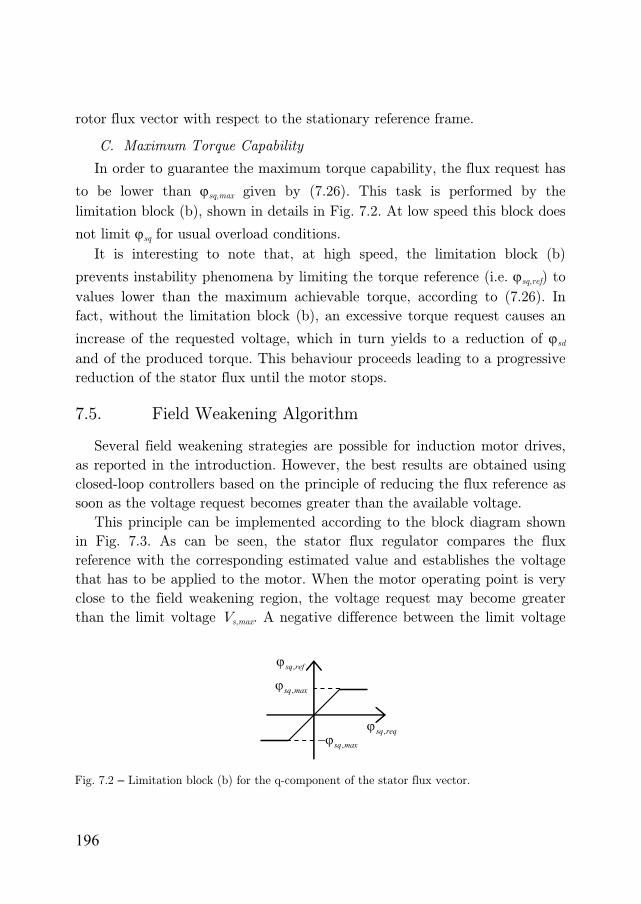
196
rotor flux vector with respect to the stationary reference frame.
C. Maximum Torque Capability
In order to guarantee the maximum torque capability, the flux request has
to be lower than ϕsq,max given by (7.26). This task is performed by the
limitation block (b), shown in details in Fig. 7.2. At low speed this block does
not limit ϕsq for usual overload conditions.
It is interesting to note that, at high speed, the limitation block (b)
prevents instability phenomena by limiting the torque reference (i.e. ϕsq,ref) to
values lower than the maximum achievable torque, according to (7.26). In
fact, without the limitation block (b), an excessive torque request causes an
increase of the requested voltage, which in turn yields to a reduction of ϕsd
and of the produced torque. This behaviour proceeds leading to a progressive
reduction of the stator flux until the motor stops.
7.5. Field Weakening Algorithm
Several field weakening strategies are possible for induction motor drives,
as reported in the introduction. However, the best results are obtained using
closed-loop controllers based on the principle of reducing the flux reference as
soon as the voltage request becomes greater than the available voltage.
This principle can be implemented according to the block diagram shown
in Fig. 7.3. As can be seen, the stator flux regulator compares the flux
reference with the corresponding estimated value and establishes the voltage
that has to be applied to the motor. When the motor operating point is very
close to the field weakening region, the voltage request may become greater
than the limit voltage Vs,max. A negative difference between the limit voltage
maxsq,ϕ
reqsq,ϕ
refsq,ϕ
maxsq,ϕ−
Fig. 7.2 – Limitation block (b) for the q-component of the stator flux vector.

197
and the amplitude vs,req of the requested voltage means that the back-emf is
too high and the flux level should be reduced. This task is performed by the
PI regulator (e), that integrates the difference s,reqs,max vV − . If this difference
is negative, the flux request decreases; otherwise, the flux level increases up
to the rated value defined in the limitation block (f). Fig. 7.4 shows the
behaviour of the limitation block (f) in details, where ϕsd,rated and ϕsd,min are
the rated and the minimum admissible value of the d-component of the
stator flux, respectively.
It is worth noting that in the field weakening region, owing to the integral
part of the regulator (e), the amplitude of the voltage request tends to equal
the limit voltage. From this point of view, the field weakening control scheme
is very similar to an anti-windup scheme preventing a voltage request greater
than the available voltage.
Although the scheme of Fig. 7.3 allows the motor to fully utilize the
supply voltage, it has an inherent drawback related to the fact that fast
variations of the torque demand in region II and III lead to undesired flux
transients which delay the torque response. In fact this scheme is based on
selecting ϕsd,ref so that the voltage required to produce the demanded torque
ratedsd ,ϕ
ratedsd ,ϕ
reqsd ,ϕ
minsd ,ϕ
refsd ,ϕ
minsd ,ϕ
Fig. 7.4 – Limitation block (f) for the d-component of the stator flux vector.
Stator Flux Regulator
s,maxV
PI (e)
s,reqvSVM +
−
s,maxVrefsv ,
Limitation (f)
| · | ABS
+
−
sϕ
refs ,ϕ
refsd ,ϕreqsd ,ϕ
Fig. 7.3- Block diagram of the field weakening controller based on the saturation of thevoltage regulator.

198
satisfies the voltage limit. For example, when a torque variation is required in
region II or III, the control system, as a consequence of the corresponding
variation of the requested voltage, changes ϕsd,ref, thus causing undesired
transients of the rotor flux.
To avoid this problem, the scheme of Fig. 7.3 should be modified in order
to change the basic principle for the selection of the flux level. In particular,
the flux level should be always set to the value required to generate the
maximum achievable torque at any operating speed. In this way any demand
of torque variations within the admissible values is achieved without
changing ϕsd but only ϕsq. This new field weakening strategy is implemented
as shown in Fig. 7.1.
For a given value of the d-component of the stator flux, and consequently
of the rotor flux, the maximum torque is achieved when ϕsq,ref = ±ϕsq,max.
Taking this equation into account, the voltage required to generate the
maximum torque can be determined from (7.27) as follows:
( )τ
ϕ−ϕ+ϕϕω−= sdrefsd
maxsqsqmaxsdsreqmaxsd iRv ,
,, sign (7.30)
τ
ϕ−ϕ+ϕω+= sqrefsq
sdmaxmaxsqsreqmaxsq iRv ,
,, (7.31)
where isq,max is defined as follows
s
maxsq
maxsqL
iσ
ϕ= ,
, (7.32)
and ωmax is the corresponding angular frequency of the rotor flux, expressed
by
( )sd
sqmaxsq
r
rsqmax
L
R
ϕ
ϕ−ϕ
σϕ+ω=ω ,
sign . (7.33)
It is worth noting that in practical applications it is possible to
approximate ωmax with ω and therefore the knowledge of the rotor parameters
is not necessary.
The main advantage of the proposed field weakening scheme is the

199
independence from the base speed and a fast torque response in the field
weakening region.
7.6. Flux and Torque Observers
A. Flux Observer
The aim of the flux observer is the determination of stator flux and phase
angle of the rotor flux, which are necessary for the field oriented control of
the induction machine. The flux observer operates in the stator reference
frame. In the following the subscript “s” will be used to identify quantities
expressed in the stator reference frame.
The stator flux is determined integrating the stator voltage:
( )∫ −=ϕ dtiRv sss
ss
ss . (7.34)
The rotor flux can be estimated as follows
( )sss
ss
rsr iL
M
Lσ−ϕ=ϕ . (7.35)
The phase angle θ of the rotor flux vector, necessary for the field oriented
control, can be derived from (7.35) as follows
( )sss
ss
sr iLσ−ϕ=ϕ=θ argarg . (7.36)
It is evident from (7.34) that the estimation of the stator flux vector can
be affected by stator resistance mismatch, sensor offsets and the inverter non-
linearity (inverter dead-times, voltage drop on the conducting switches, etc.).
However, at high speed, and hence in the field weakening region, the
estimation error is lower than that at low speed, because the input voltage
becomes the most important term in the right-hand side of (7.34).
The estimation error on the phase angle θ depends on the stator flux
estimation error, the mismatch on the leakage inductance σLs and the offset
of the current sensors. The leakage inductance shows moderate variations
with the stator currents and it will be assumed practically constant.
In conclusion, the stator flux observer depends only on two machine
parameters, namely Rs and σLs, but the effects of this dependence can be

200
considered negligible in the high speed range. On the contrary, in order to
obtain good performance at low speed, it is preferable to adopt a closed-loop
flux estimator, that could reduce the effect of parameter mismatch and sensor
offsets [79].
B. Estimation of the Angular Frequency of the Rotor Flux Vector
The angular frequency ω needed in (7.27) and (7.33) is obtained by means
of the following equation:
⎟⎟⎠
⎞⎜⎜⎝
⎛
ϕϕ
⋅⎟⎟⎠
⎞⎜⎜⎝
⎛
ϕϕ
=ωr
r
r
r jdt
d . (7.37)
The angular frequency ω is insensitive to disturbance and noise that
usually affect the stator flux and the stator currents, owing to the filtering
action applied to the rotor flux. When this action is not adequate, an
additional low-pass filter can be applied to (7.37).
C. Torque Observer
The torque can be estimated from the measurements of the stator current
and the estimation of the stator flux, as follows:
( )ss jipT ϕ⋅=2
3. (7.38)
As can be seen, the torque estimation does not require explicitly any
motor parameters, excepts the pole pairs.
7.7. Simulation Results
Preliminarily, some numerical simulations have been carried out to
confirm the effectiveness of the field weakening strategy. The motor
parameters are reported in Tab. 7.1, and the load is supposed to be only
inertial.
Fig. 7.5 shows the motor behaviour in response to a step command of the
motor torque (the figure does not include the end of the transient). Vertical
dash-dotted lines delimit the three regions of operation of the induction
motor. Initially, the torque delivered to the load is zero, the motor is at
standstill and the stator flux corresponds to the rated value. As the torque

201
command is applied, the motor starts up.
The q-component of the stator flux requested by the PI regulator (a) is
limited to the value ϕsq,max, corresponding to a stator current equal to Is,max.
As soon as vs,max req reaches the voltage limit, the field weakening algorithm
decreases the d-component of the stator flux. As a consequence of the
reduction of the magnetizing current, the q-component of the stator current,
0
0.5
1
0
0.4
0
0.4
0
1000
2000
-2
0
2
(2)
(3)
(4)
(5)
(7)
Nm
Wb
Wb
A
rpm
Region I Region II Region III
(1)
(6)
0.5 s/div
Fig. 7.5 – Computer simulation. Starting transient from 0% up to 600% of the base speed after the application of the rated torque. Main motor quantities. 1) Torque reference. 2) Estimated torque. 3) ϕsd,ref. 4) ϕsq,ref.. 5) Rotor flux. 6) Motor speed. 7) Stator current.
TABLE 7.1 – MOTOR PARAMETERS
Prated = 0.25 kW Rs = 14.6 Ω Is, rated = 1.16 Arms Rr = 16 Ω Vs,rated = 220 Vrms Ls = 701 mH ωs = 2π50 rad/s Lr = 701 mH p = 1 M = 53 mH

202
proportional to ϕsq,ref, increases, making it possible to keep the stator
current equal to the limit current in region II. As soon as the motor enters in
region III, the current decreases and the maximum value of ϕsq,ref is set equal
to ϕsd,ref.
Fig. 7.6 shows the motor behaviour after a torque reduction from 100% of
the rated torque to 50% of the rated torque in region II. As can be seen,
immediately after the torque decreases, the voltage delivered to the loads is
lower than Vs,max, but this voltage margin does not mean that ϕsd should
increase. In fact the motor continues accelerating and ϕsd decreases without
unwanted transients. This behaviour could not be achieved without changing
the basic scheme of the field weakening strategy of Fig.7.3 as proposed in
0
0.5
1
0
0.4
0.8
0
500
1000
-2
0
2
(2)
(3)(4)
(5)
(7)
(8)
0.5 s/div
Nm
Wb
Vmax
A
rpm
Region I Region II
(1)
(6)
Region III
Fig. 7.6 – Computer simulation. Torque reduction from 100% of the rated torque to 50% of the rated torque in region II during an acceleration transient. Main motor quantities. 1) Torque reference. 2) Estimated torque. 3) ϕsd,ref. 4) ϕsq,ref.. 5) Vs,max. 6) vs. 7) Motor speed. 8) Stator current.

203
Fig. 7.1.
7.8. Experimental Results
A complete drive system has been realized to verify the feasibility of the
proposed control scheme. The experimental set-up consists of a MC inverter
and a 250 W, 2-pole squirrel cage induction motor. The motor parameters are
the same ones reported in Tab. 7.1. The test motor is coupled to a separately
excited DC machine, 3000 rpm. The control algorithm is implemented on a
Digital Signal Processor (DSP) TMS320C28. The cycle period of the control
scheme, including the field weakening algorithm, is 125 μs.
Some tests have been carried out to investigate the drive performance in
the field weakening region. In order to limit the test bench speed to safe
values, the motor has been fed with a reduced voltage, i.e. 25% of the rated
voltage, so leading to a rated speed of about 700 rpm.
Fig. 7.7 shows the motor behaviour during a transient from 90% up to
600% of the rated speed (the figure does not include the end of the
transient). As can be seen, the motor behaves as expected, namely the
(2)
(4)
(1)
(3)
Region I
Region II
Region III
Fig. 7.7 – Experimental test. Speed transient from 90% to 600% of the base speed. 1) Estimated speed (1500 rpm/div). 2) ϕsd,ref. (0.25 Wb/div). 3) ϕsq,ref. (0.25 Wb/div). 4) Stator current (1.5 A/div).
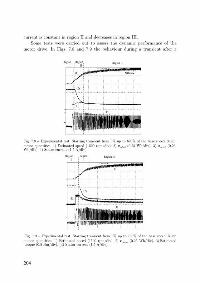
204
current is constant in region II and decreases in region III.
Some tests were carried out to assess the dynamic performance of the
motor drive. In Figs. 7.8 and 7.9 the behaviour during a transient after a
(2)
(4)
Region I
Region II
Region III
(1)
(3)
Fig. 7.8 – Experimental test. Starting transient from 0% up to 600% of the base speed. Mainmotor quantities. 1) Estimated speed (1500 rpm/div). 2) ϕsd,ref (0.25 Wb/div). 3) ϕsq,ref. (0.25 Wb/div). 4) Stator current (1.5 A/div).
(2)
(4)
Region I
Region II
Region III
(1)
(3)
Fig. 7.9 – Experimental test. Starting transient from 0% up to 700% of the base speed. Main motor quantities. 1) Estimated speed (1500 rpm/div). 2) ϕsd,ref (0.25 Wb/div). 3) Estimated torque (0.8 Nm/div). (4) Stator current (1.5 A/div).

205
torque step is shown. The experimental results are in good agreement with
the computer simulations shown in Fig. 7.5. In particular ϕsq,ref, constant in
region I, slightly increases in region II, keeping the stator current equal to the
limit value.
Some tests have been carried out to evaluate the capability of the control
system to increase the flux during a deceleration transient.
Fig. 7.10 shows the motor behaviour when the speed decreases from about
500% to 90% of the base speed. The deceleration is obtained by increasing
the breaking torque generated by the DC machine operating as a load. It can
be verified that, as the speed decreases, the control algorithm increases
smoothly the flux reference ϕsd,ref up to the rated value.
Finally, the quality of the input and output currents have been assessed.
Fig. 7.11 shows the waveform of a load current, whereas Fig. 7.12 shows the
waveforms of the line currents for two different load conditions. As can be
seen, all the waveforms are nearly sinusoidal and the harmonic content is
negligible.
(2)
(4)
Region I
Region II Region III
(1)
(3)
Fig. 7.10 – Experimental test. Breaking transient from 500% down to 90% of the base speed. Main motor quantities. 1) Estimated speed (1500 rpm/div). 2) ϕsd,ref (0.25 Wb/div). 3) ϕsq,ref.(0.25 Wb/div). (4) Stator current (1.5 A/div).

206
7.9. Conclusion
A control strategy for field weakening operation of speed-sensorless
induction motor drives fed by MC is analyzed in this chapter.
The control system scheme utilizes the stator flux components as control
variables and decreases the d-component of the stator flux as the voltage
corresponding to the maximum torque achievable at a given speed tends to
exceed the maximum voltage.
The control scheme allows a smooth transition into and out of the field
a) b)
Fig. 7.12 – Experimental test. Input currents for two different load conditions (2.5 A/div). Motor operating at the base speed, at 30% of the rated torque (a) or at the rated torque (b).
Fig. 7.11 – Experimental test. Load currents (0.75 A/div).

207
weakening mode, exploiting the maximum torque capability of the machine
over the whole operating speed range.
The main advantages of proposed field weakening algorithm are: i)
reduced dependence on machine parameters, ii) no need of calculation of the
base speed, which in general depends on the machine parameters, motor
current and available voltage, iii) fast torque response, also in the field
weakening region.
The effectiveness of the proposed control scheme has been verified by
computer simulations and experimental tests.

208
8.Appendix A
The algorithm for the selection of λ and om in the general case is
presented in this Appendix.
The first step is to determine which triangle vertex should coincide with a
duty-cycle space vector. This can be done by means of Fig. A.1, that reports
the vertex names as a function of the sector of refψ . If the indexes 1,2,3 are
associated to the vertex A, B and C respectively, the position of the selected
vertex in the d-q plane can be represented by means of the space vector
( )( )3/12exp32 −νπj , where ν is defined in Fig. A.1.
Then, the modulation algorithm determines which duty-cycle space vector
among 1m , 2m and 3m should coincide with the vertex previously selected.
For this purpose, the index n of the searched duty-cycle space vector is
reported in Table A.1. As can be seen, the index n depends on the sector
occupied by the reference output voltage and the input current. The sectors
of the reference output voltage are represented in Fig.A.2.
The duty-cycle space vector nm must satisfy the following constraint:
( )1
3
2
3
2 −νπ=
j
n em (A1)

209
Substituting (18), written for k=n in (A1), and solving for om , leads to
the following expression:
( )
nn
j
o BAem λ−−=−νπ 1
3
2
3
2. (A2)
By substituting (A2) in (3.2) the following general expressions for the
remaining duty-cycle space vectors, as a function of λ, can be found:
( ) ( )13
2
3
2 −νπ+−λ+−=
j
nknkk eBBAAm (k=1,2,3 and k ≠ n). (A3)
60°
refψ
Vertex A(ν =1)
Vertex C(ν =3)
Vertex C(ν =3)
Vertex A(ν =1)
Vertex B(ν =2)
Vertex B(ν =2)
Fig. A.1 – Graphic table for the selection of the triangle vertex coinciding with a duty cyclespace vector among 1m , 2m and 3m as a function of the desired direction of the input
current.
α o
v o,ref
sector
60°
Fig. A.2 - Sectors of the output reference voltage vector.

210
With reference to the example of Fig. 3.2, (A3) represent the parametric
equations of the straight lines r and s.
The next step of the modulation algorithm consists in the determination
of the six values of λ that bring a duty-cycle space vector to a triangle side.
These values can be determined by solving each of the six following linear
equations:
03
13
2
=+⋅πh
j
k em (k ≠ n, h=0,1,2) (A4)
Among these six values of λ, in this analysis, the one corresponding to the
minimum absolute value is adopted for the modulation law. The selected
value coincides with the values λp or λn previously defined.
TAB. A.1 – INDEX n OF THE DUTY-CYCLE SPACE VECTOR PLACED ON A TRIANGLE VERTEX
SECTOR OF THE DESIRED INPUT CURRENT 1 - 3 - 5 2 - 4 - 6
1 1 3 2 2 3 3 2 1 4 3 1 5 3 2
SECTOR OF THE
REFERENCE OUTPUT VOLTAGE
6 1 2
211
9.Appendix B
To determine the time required by ripi to virtually cover the distance
between C and A, the following equation can be used:
0=++ ACCBBA (B1)
where the expression of BA , CB and AC are those given in Tab. 3.5.
Substituting and solving for δ′ leads to
( ) ( )
2,
,,22,,11
refo
reforeforeforefo
v
vvvvvv ⋅−δ+⋅−δ=δ′ . (B2)
Similarly, for δ ′′ one obtains:
( ) ( )
2,
,,44,,33
refo
reforeforeforefo
v
vvvvvv ⋅−δ+⋅−δ=δ ′′ . (B3)

212
10.Appendix C
In this Appendix some definitions involving Laplace transform are
presented, which are used in the stability analysis.
Let be )(sf the Laplace transform of the generic vector )(tf , defined as
follows:
∫∞
−=0
)()( dtetfsf st . (C1)
The superscript ‘c’ is used for the Laplace transform of )(* tf , defined as
∫∞
−=0
* )()( dtetfsf stc . (C2)
It can be verified that the following relationships exist between )(sf and
)(sf c :
)()( ** sfsf c = (C3)
)()( ** sfsf c = (C4)

213
11.Appendix D
A transfer function of a filter in the time domain can be approximated in
the discrete-time by using several expressions.
In Chapter 5, (5.42) has been approximated by means of the following
difference equation:
)1()()1()( 101 −++−= kvbkvbkvakv iiifif (D1)
where
2
2
1
1
2
111 TjTja ii ⎟
⎠⎞
⎜⎝⎛ ω+−+⎟
⎠⎞
⎜⎝⎛ ω+−+=
ττ (D2)
τ20
Tb = (D3)
⎥⎦
⎤⎢⎣
⎡⎟⎠⎞
⎜⎝⎛ ω+−+= Tj
Tb iττ
11
21 . (D4)
that can be represented with the following Z-transform:
1
1
110
1)( −
−
−+
=za
zbbzFd . (D5)

214
12.Appendix E
The ratio ε can be more easily characterized by the knowledge of the
converter efficiency (η) and the conduction losses to switching losses ratio
(δ). The converter efficiency is given by
swid
cdid
in
out
PP
PP
P
P
+−
==η (E1)
which can be rewritten as follows
εδεη
+−
=1
1 (E2)
where
sw
cd
P
P=δ . (E3)

215
13.Appendix F
The input current can be expressed as a sum of harmonics. To obtain this
result, it is necessary to substitute (5.65) in (5.64) and to take (5.66) into
account. It follows:
tji
ietfi ω= )( (F1)
where
tj
invtj
diri
id
rr eVeVV
Ptf ωω− ++
=***3
2)( (F2)
The function )(tf is periodic and can be expressed as a Fourier series as
follows:
∑∞
−∞=
ω=k
tjkk
reFtf )( (F3)
where
∫ωπ
ωπ
−
ωπ
−
πω
= r
r
r dtetfFktj
rk
2
)(2
. (F4)
An approximated form for )(tf can be derived from (F3) neglecting the

216
terms with order greater then 1, as follows
tjtj rr eFFeFtf ωω−− ++≅ 101)( . (F5)
The explicit form of 1−F , 0F and 1F can be calculated by means of (F4)
for k = -1, 0 and 1 respectively. Substituting (F5) in (F1) leads to (5.67) and
the expressions of 1−F , 0F and 1F coincides with those given in (5.68), (5.69)
and (5.70).

217
14.Appendix G
To derive (5.92), (5.78) must be written in the following form:
11
13
)(2
−=⎟⎠⎞
⎜⎝⎛
δ−ω+ω β
dir
ojri
V
PeZ . (G1)
Rearranging the terms of (G1) leads to this equivalent equation:
β−λ−=⎟⎠⎞
⎜⎝⎛
δ− je
11 (G2)
where λ is the real positive parameter defined as
ori
dir
PZ
V
)(
3 2
ω+ω=λ . (G3)
Finally, combining (G2), (5.71) and (5.86) and solving for p leads to
(5.92).

218
References
Preface
[1] Alesina, M. Venturini, ”Solid-state power conversion: a fourier analysis
approach to generalized transformer synthesis,” IEEE Trans.Circuits and
Systems, vol. 28, No. 4, pp. 319-330, April 1981.
[2] A. Alesina, M. G. B. Venturini, ”Analysis and design of optimum-amplitude
nine-switch direct ac-ac converters,” IEEE Trans. Power Electronics, vol. 4,
pp. 101-112, January 1989.
[3] P. D. Ziogas, S.I. Khan, M.H. Rashid, ”Analysis and design of forced
commutated cycloconverter structures with improved transfer
characteristics,” IEEE Trans. Industrial Electronics, vol. 1E-33, No. 3, pp.
271-280, August 1986.
[4] L. Huber, D. Borojevic, ”Space vector modulator for forced commutated
cycloconverters,” Proc. IEEE PESC Conf., San Diego, (USA), 1989, pp. 871-
876.
[5] L. Huber, D. Borojevic, ”Space vector modulated three-phase to three-phase
matrix converter with input power factor correction,” IEEE Trans. on
Industry Applications, Vol. 31, No. 6, November/ December 1995, pp. 1234-
1246.

219
[6] D. Casadei, G. Grandi, G. Serra, A. Tani, ”Space vector control of matrix
converters with unity input power factor and sinusoidal input/output
waveforms,” Proc. EPE Conference, Brighton (UK), 13-16 September 1993,
vol. 7, pp. 170-175.
[7] D. Casadei, G. Serra, A. Tani, L. Zarri, ”Matrix converter modulation
strategies: a new general approach based on space-vector representation of
the switch state,” IEEE Trans. Industrial Electronics, Vol. 49, No. 2, pp.
370-381, April 2002.
[8] C. Klumpner, P. Nielsen, I. Boldea,; F. Blaabjerg,: ”New solutions for a low-
cost power electronic building block for matrix converters,” IEEE Trans. on
Industrial Electronics, Vol. 49 , No. 2, Apr. 2002, pp. 336 - 344.
[9] J. Mahlein, J. Weigold, O. Simon, ”New concepts for matrix converter
design,” IEEE IECON-01, 29 Nov-2 Dec. 2001, Denver, USA, vol. 2,
pp.1044-1048.
[10] M. Bland, L. Empringham, P. W. Wheeler, J. C. Clare, ”Comparison of
calculated and measured switching losses in direct ac-ac converters,” IEEE
PESC Conf 2001, pp. 1096-1101.
[11] Jun-Koo Kang, H. Hara, E. Yamamoto, E. Watanabe, ”Analysis and
evaluation of bi-directional power switch losses for matrix converter drive,”
Record of the Industry Applications Conference 2002, 13-18 Oct. 2002, pp.
438 - 443 vol.1.
[12] P.W. Wheeler, J. C. Clare, L. Empringham, ”A vector controlled MCT
matrix converter induction motor drive with minimized commutation times
and enhanced waveform quality,” Proc. of IEEE IAS 2002, Vol. 1 , 13-18
Oct. 2002, pp. 466 - 472.
[13] K.G. Kerris, P.W. Wheeler, J.C. Clare, L. Empringham, ”Implementation of
a matrix converter using p-channel MOS-controlled thyristors, Power
Electronics and Variable Speed Drives”, 2000. Eighth International
Conference on IEE Conf. Publ. No. 475 , 18-19 Sept. 2000, pp. 35 - 39.
[14] P.W. Wheeler, J.C. Clare, L. Empringharn, M. Bland, M. Apap ”Gate drive
level intelligence and current sensing for matrix converter current
commutation”, IEEE Trans. on Industrial Electronics, Vol. 49 , No. 2 , April
2002, pp. 382 - 389.
[15] D. Casadei, A. Trentin, M. Matteini, M. Calvini, ”Matrix Converter
Commutation Strategy using both output current and input voltage sign
measurement”, EPE 2003, 2-4 Sept., Toulouse, France, paper 1101, CD-
ROM.

220
[16] J. Mahlein, J. Igney, J. Weigold, M. Braun, O. Simon, ”Matrix converter
commutation strategies with and without explicit input voltage sign
measurement”, IEEE Trans. Industrial Electronics, vol. 49, No.2, pp. 407-
414, April 2002.
[17] P. Nielsen, F. Blaabjerg, J. K. Pedersen, ”New Protection Issues of a Matrix
Converter: Design Considerations for Adjustable-Speed Drives”, IEEE
Trans. on Ind. App., vol. 35, n. 5, Sept./Oct. 1999, pp. 1150-1160.
Chapter 1
[18] D. Casadei, G. Serra, A. Tani, ”Stability analysis of electrical drives fed by
matrix converters,” in Proc. IEEE-ISIE, L’Aquila, Italy, Jul. 2002, pp.1108-
1113.
[19] D. Casadei, G. Serra, A. Trentin, L. Zarri, M. Calvini, ”Experimental
analysis of a matrix converter prototype based on new IGBT modules,”
IEEE ISIE 2005, June 20-23, 2005, Dubrovnik, Croatia, Vol. II, pp. 559-564.
[20] C. Klumpner, F. Blaabjerg, ”Short term braking capability during power
interruptions for integrated matrix converter motor drives,” IEEE Trans. on
Power Electronics, Vol. 19, No. 2, March 2004, pp. 303-311.
[21] D. Casadei, G. Serra, A. Tani, ”Reduction of the input current harmonic
content in matrix converters under input/output un-balance,” IEEE Trans.
on IE, vol. 45, n. 3, June 1998, pp. 401-411.
[22] D. Casadei, G. Serra, A. Tani, ”A general approach for the analysis of the
input power quality in matrix converters,” IEEE Trans. on PE, vol. 13, n. 5,
September 1998, pp. 882-891.
[23] F. Blaabjerg, D. Casadei, C. Klumpner, M. Matteini, ”Comparison of two
current modulation strategies for matrix converters under unbalanced input
voltage conditions,” IEEE Trans. on IE, vol. 49, n. 2, April 2002, pp. 289-
296.
[24] D. Casadei, G. Serra, A. Tani, L. Zarri, ”Effects of input voltage
measurement on stability of matrix converter drive system,” IEE
Proceedings on Electric Power Applications, vol. 151, No. 4, July 2004, pp.
487-497.
[25] F. Liu, C. Klumpner, F. Blaabjerg, ”Stability analysis and experimental
evaluation of a matrix converter drive,” in Proc. IECON, Roanoke, VA,
Nov. 2003, pp. 2059-2065.

221
[26] L. Malesani, L. Rossetto, P. Tenti, P. Tomasin, ”AC/DC/AC PWM
converter with reduced energy storage in the DC link,” IEEE Trans-actions
on Industry Applications, vol. 31 , no.2 , March-April 1995, pp. 287 - 292.
[27] S. Bernet, S. Ponnaluri, R. Teichmann, ”Design and loss comparison of
matrix converters and voltage-source converters for modern AC drives,”
IEEE Transaction on Industrial Electronics, vol. 49, no.2 , April, 2002, pp.
304-314.
[28] M. Apap, J.C. Clare, P.W. Wheeler, M.Bland, K. Bradley, ”An approach to
the analysis on efficiency and device control power loss distribution for
matrix converters,” Proceedings of EPE Conference, 2003, ISBN: 90-75815-
07-7, no. 509, pp. 1-8.
[29] D.Casadei, G.Grandi, C.Rossi, A.Trentin, L.Zarri, ”Comparison between
back-to-back converter and matrix converter based on the thermal stress of
the switches”, in Proc. IEEE ISIE, May 4-7 2004, Ajaccio, France, ISBN 0-
7803-8305-2 (on cd-rom, file sf-001304.pdf).
Chapter 2
[30] M.J. Maytum, D. Colman: ”The implementation and future potential of the
venturini converter,” in Proc. Drives, Motors and Controls, 1983, pp. 108-
117.
[31] G. Roy, G.E. April: ”Cycloconverter operation under a new scalar control
algorithm,” in Proc. IEEE PESC. Conf., Milwaukee (WI), 1989, pp. 368-375.
[32] L. Huber, D. Borojevic: ”Space vector modulation with unity input power
factor for forced commutated cycloconverters,” in Proc. IEEE IAS Conf.,
pp. 1032-1041, 1991.
[33] O. Simon, M. Braun: ”Theory of vector modulation for matrix converters,”
Proc. EPE Conference, Graz (Austria), 27-29 August 2001.
Chapter 3
[34] L. Huber, D. Borojevic, ”Digital modulator forced commutated cyclo
converters with input power factor correction”, in Proc. IEEE PESC Conf.,
1992, pp. 518-523.
[35] P. Nielsen, F. Blaabjerg, J.K. Pedersen, ”Space vector modulated matrix

222
converter with minimized number of switchings and a feedforward
compensation of input voltage unbalance”, in Proc. PEDES Conf., 1996, pp.
833-839.
[36] L. Helle, S. Munk-Nielsen, ”A novel loss reduced modulation strategy for
matrix converters”, in Proc. IEEE PESC Conf., 2001, pp. 1102-1107.
[37] M. Apap, J.C. Clare, P.W. Wheeler, K.J. Bradley, ”Analysis and comparison
of AC-AC matrix converter control strategies”, in Proc. IEEE PESC Conf.,
2003, Vol. 3, pp. 1287-1292.
[38] L. Helle, K.B. Larsen, A.H. Jorgensen, S. Munk-Nielsen, ”Evaluation of
modulation schemes for three-phase to three-phase matrix converters,” IEEE
Trans. Industrial Electroncs, Vol. 51, No. 1, pp. 158-171, February 2004.
[39] D. Casadei, G. Serra, A. Tani, L. Zarri, ”Effects of the switching strategy on
the input power quality of matrix converters,” IEEE Power Tech 2003, 23-
26 June 2003, Bologna, Italy, Vol. 1, 8 pp.
[40] J.Igney, M. Braun, ” A New Matrix Converter Modulation Strategy
Maximizing the Control Range,” PESC 2004, June 20-25, Aachen, Germany,
Vol. 3, pp. 2875-2880
[41] D. Casadei, G. Serra, A. Tani, L. Zarri, ”A novel modulation strategy for
matrix converters with reduced switching frequency based on output current
sensing,” PESC 2004, June 20-25, Aachen, Germany, Vol. 3, pp. 2373-2379,
ISBN: 07803-8400-8, IEEE Catalog Number 04CH37551C, CD-ROM,
2373˙11393.pdf.
[42] D. Casadei, G. Serra, A. Tani, L. Zarri, ”Theoretical and experimental
analysis for the RMS current ripple minimization in induction motor drives
controlled by SVM technique,” IEEE Trans. on IE, Vol. 51, No.4, pp.1056-
1066, Oct. 2004.
Chapter 4
[43] T. Lipo, P. Krause: ”Stability analysis of a rectifier-inverter induction motor
drive,” IEEE Trans. on PAS, PAS-88, vol. 1, 1969, pp. 55-66.
[44] M.M. Ahmed, J.A. Taufiq, C.J. Goodman, M. Lockwood: ”Electrical
instability in a voltage source inverter-fed induction motor at a constant
speed,” IEE Proc. B, vol. 133, No. 4, 1986, pp. 299-307.
[45] B. Mellit, J. Allan: ” Stability characteristics of a constant power chopper
controller for traction drives,” IEE Proc. B, vol. 1, No. 3, 1978, pp. 100-104.

223
[46] S. Chandrasekaran, D. Borojevic, D.K. Lindner: ”Input filter interaction in
three phase AC-DC converters,” in Proceedings of PESC, 1999, pp. 987-992.
[47] R. Czarnecki, K. Hasse, A.M. Walczyna: ”Input filter stability of drives fed
from voltage inverters controlled by direct flux and torque control methods,”
IEE Proc. Electr. Power Appl., Vol. 143, No. 5, September 1996, pp. 396-
402.
[48] D. Casadei, G. Serra, A. Tani: ”The Use of Matrix Converters in Direct
Torque Control of Induction Machines,” in Proceedings of IECON, Aachen
(Germany), August 31 - September 4 1998, Vol. 2, pp. 744-749.
[49] P.W. Wheeler, J. Rodriguez, J. C. Clare, L. Empringham, ”Matrix
Converter. A technology review,” IEEE Transactions of Industrial
Electronics, vol.49, no.2, April, 2002, pp. 276-288
[50] Yanhui Xie, Yongde Ren, ”Implementation of DSP-based three-phase AC-
AC matrix converter,” Proc. of IEEE APEC ’04, vol. 2 , 2004, pp. 843 - 847.
[51] C.L. Neft, C.D. Schauder: ”Theory and Design of a 30-HP Matrix
Converter,” IEEE Trans. on IA, Vol. 38, No. 3, May-June 1992, pp. 546-551.
[52] D. Casadei, G. Serra, A. Tani, L. Zarri, ”Analysis of digital implementation
effects on matrix converter stability,” Proc. EPE’03, Toulouse, France, 2-4
September 2003, ISBN 90-75815-07-7, CD-ROM, 0894.pdf.
Chapter 5
[53] D. Casadei, G. Serra, A. Tani, L. Zarri, ”Improvement of the stability of
electrical drives fed by matrix converters,” IEE Seminar on Matrix
Converters, April 2003, Birmingham, pp. 3/1-3/12.
[54] M. Bland, L. Empringham, P. W. Wheeler, J. C. Clare, ”Comparison of
calculated and measured switching losses in direct AC-AC converters,” Proc.
IEEE-PESC Conf., 2001, 17-21 Jun. 2001, Vancouver, BC , Canada, Vol. 2,
pp. 1096-1101.
[55] J. K. Kang, H. Hara, E. Yamamoto, E. Watanabe, ”Analysis and evaluation
of bi-directional power switch losses for matrix converter drive,” Proc. IEEE-
IAS 2002, Pittsburgh, USA, 13-18 Oct. 2002, vol.1, pp. 438-443.
[56] D.Casadei, G.Serra, A.Tani, A.Trentin, L.Zarri, ”Theoretiecal and
experimental investigation on the stability of matrix converters,” IEEE
Trans. Ind. Electron., vol. 52, no. 5, pp. 1409-1417, October 2005.

224
Chapter 6
[57] M. H. Rashid, A. I. Maswood, ”Analysis of three-phase AC-DC converters
under unbalanced supply conditions,” IEEE Trans. on Ind. App., Vol. 24.
No. 3 May/June 1988, pp. 449-455.
[58] M. Sakui, H. Fujita, ”Calculation of harmonic currents in a three-phase
convertor with unbalanced power supply conditions,” IEE Proc.-B, Vol. 139,
No. 5, Sept. 1992, pp. 478-484.
[59] L. Moran, P. D. Ziogas, G. Joos, ”Design aspects of synchronous PWM
rectifier-inverter systems un-der unbalanced input voltage conditions,” IEEE
Trans. on Ind. App., Vol. 28 No. 6, Nov./Dec. 1992, pp. 1286-1293.
[60] P. Enjeti, X. Wang, ”A critical evaluation of harmonic generated by forced
commutated cyclo con-verter under unbalance,” Proc. of IAS 1990, pp. 1162-
1166.
[61] D. Casadei, G. Grandi, G. Serra, A. Tani, ”Analysis of space vector
modulated matrix converter under unbalanced supply voltages,” Proc. of
SPEEDAM’94, 8-10 June, 1994, Taormina (Italy), Proceedings pp. 39-44.
[62] D. Casadei, G. Serra, A. Tani, P. Nielsen, ”Performance of SVM controlled
matrix converter with input and output unbalanced conditions,” Proc. of
EPE-95, Sevillle, 18-21 Sept. 1995, Proceedings Vol. II, pp. 628-633.
[63] A. Ferrero, G. Superti-Furga, ”A unified approach to unbalance three-phase
systems under non-sinusoidal conditions: some definitions,” Proc. 4-th
Conference on Harmonics in Power Systems, Budapest (Hungary), October
1990, pp.32-37.
[64] D. Zhou, K. Sun, L. Huang, ”Evaluation of matrix converter operation in
abnormal conditions,” Proc. of ICEMS 2003, Beijing, China, 9-11 Nov., 2003,
vol. 1, pp. 402-406.
[65] Y.Mei, K.Sun, D. Zhou, L. Huang, ”Analysis and comparison of matrix
converter operation under abnormal input voltage conditions,” Proc. of
IPEMC, Xian, China, 14-16 Aug. 2004, vol. 3, pp. 1311-1315.
[66] K.Yamada, T. Higuchi, E.Yamamoto, H.Hara, T.Sawa, ”Integrated filters
and their combined effects in matrix converter,” Proc. of IAS 2005, Hong
Kong, 2-6 Oct. 2005, vol.2, pp. 1498-1503.
[67] J.K. Kang, H.Hara, E. Yamamoto, E. Watanabe, J. Oyama et al., ”Input
harmonics damping for high power quality applications of matrix converter,”
Proc. of IAS 2003, Salt Lake City, 12-16 Oct 2003, pp.1498-1503.

225
[68] P.Wheeler, D. Grant, ”Optimised input filter design and low-loss switching
techniques for a practical matrix converter,” IEE Proc. Electric Power
Applications, vol. 144, no.1, January 1997, pp. 53-60.
Chapter 7
[69] E. Watanabe, S. Ishii., E, Yamamoto, H. Hara, J. Kang, Ahmet M. Hava,
”High performance motor drive using matrix converter,” 2000, pp.7/1-7/6.
[70] Kyo-Beum Lee, F. Blaabjerg, ”Improved sensorless vector control for
induction motor drives fed by a matrix converter using nonlinear modeling
and disturbance observer,” IEEE Trans. of Energy Conversion, Vol. 21, No.
1, March 2006, pp. 52-58.
[71] C. Klumpner , P. Nielsen, I. Boldea, F. Blaabjerg, ”A new matrix converter
motor (MCM) for industry applications,” IEEE Trans. on Ind. Elect., Vol.
49, No. 2, April 2002, pp.325-335.
[72] Junichi Itoh, I. Sato, A. Odaka, H. Ohguchi, H. Kodachi, N. Eguchi, ”A
novel approach to practical matrix converter motor drive system with
reverse blocking IGBT,” IEEE Trans. on PE, Vol. 20, No. 6, Nov. 2005,
pp.1356-1362.
[73] Kyo-Beum Lee, F. Blaabjerg, ”Reduced-order extended Luenberger observer
based sensorless vector control driven by matrix converter with nonlinearity
compensation,” IEEE Trans. on Industrial Electronics, Vol.53, No.1,
February 2006, pp. 66-74.
[74] K. Sun, L Huang, K. Matsuse, T. Ishida, ”Combined control of matrix
converter fed induction motor drive system,” Proc. of IAS 2003, 12-16 Oct.
2003, Vol. 3, pp. 1723-1729.
[75] T. Podlesak, D. Katsis, P. Wheeler, J. Clare, L. Empringham, M. Bland, ”A
150 kVA vector-controlled matrix converter induction motor drive,” IEEE
Trans. on Ind. App., Vol. 41, No. 3, May/June 2005, pp. 841-847.
[76] X. Xu, D. W. Novotny, ”Selection of the flux reference for induction
machine drives in the field weakening region,” IEEE Trans. on Ind. App. Vol
28, No 6, Nov. - Dec. 1992, pp. 1353-1358.
[77] S.H.Kim, S.K. Sul, ”Maximum torque control of an induction machine in the
field weakening region,” IEEE Trans. on. Ind. Appl., Jul./Aug. 1995, Salt
Lake City, USA, vol.31, No.4, pp. 787-794.
[78] G. Griva, F. Profumo, M. Abrate, A. Tenconi, D. Berruti, ”Wide speed

226
range DTC drive performance with new flux weakening control,” Conf. Rec.
PESC-98, 17-22 May 1998, Fukuoka, Japan, vol. 2, pp. 1599-1604.
[79] D. Casadei, F. Profumo, G. Serra, A. Tani, L. Zarri, ”Performance analysis
of a speed-sensorless induction motor drive based on a constant-switching-
frequency DTC scheme,” IEEE Trans. on Ind. App., Vol. 39, NO. 2,
March/April 2003, pp. 476-484.
[80] H. Grotstollen, J.Wiesing, ”Torque capability and control of a saturated
induction motor over a wide range of flux weakening,” IEEE Trans. on Ind.
Elec., vol. 42, no. 4, Aug. 1995, pp. 374-381.
[81] R. J. Kerkman, T. M. Rowan, D. Leggate, ”Indirect field-oriented control of
an induction motor in the field-weakening region,” IEEE Trans. on Ind.
Applications, Vol. 28, No. 4, July / August 1992, pp. 850-857.
[82] E. Levi, M. Wang, ”A speed estimator for high performance sensorless
control of induction motors in the field weakening region,” IEEE Trans. on
Power Electronics, Vol.17, No. 3, May 2002, pp. 365-378.
[83] M.S. Huang and C.M. Liaw, ”Transient performance improvement control
for IFO induction motor drive in field-weakening region,” IEE Proc.-Electr.
Power Appl., Vol. 150, No. 5, September 2003, pp. 521-530.
[84] M.Ho Shin, D.S. Hyun, S. B. Cho, ”Maximum torque control of stator-flux-
oriented induction machine drive in the field-weakening region,” IEEE
Trans. on Ind. App., Vol. 38, No. 1, January/February 2002, pp. 117-121.
[85] A. Biinte, H. Grotstollen, P. Krafka, ”Field weakening of induction motors
in a very wide region with regard to parameter uncertainties,” PESC 96,
Vol. 1, 26-27 June 96, pp. 944-950.
[86] S.H. Kim, S.K. Sul, ”Voltage control strategy for maximum torque operation
of an induction machine in the field weakening region,” IEEE Trans. on Ind.
El., Vol. 44, No.4, Aug. 1997, pp. 512-518.
[87] D. Casadei, G. Serra, A. Tani, L. Zarri, ”Robust flux weakening operation of
induction motor drives based on stator flux vector control,” Proc. of ICEM
2006, XVII International Conference on Electrical Machines, Chania, Crete
Island, Greece, September 2-5, 2006, paper PMM2-15 on CD-ROM, pp.
489/1- 489/6.
[88] H. Abu-Rub, H. Schmirgel,. Holtz, ”Sensorless control of induction motors
for maximum steady-state torque and fast dynamics at field weakening,” IAS
2006, Tampa, Florida, 8-12 October 2006, Paper N.IAS03P, ISBN: 1-4244-
0365-0.