material declaration - inemithor.inemi.org/webdownload/newsroom/presentations/ece/material... ·...
TRANSCRIPT

Material Declaration
Who’s in Charge?

The PlayersEIA, EICTA, JGPSSI, Industry GuideDIN German Norm 19220Solder Products Value CouncilJEDEC, NEMI, IPC CoordinationZVEI German Components Assoc.ECCA European Component Assoc.Lead Free Solder World SummitJIC, JNAC, Jisso Japan, EJCJapan Electronic & Info Tech AssocIEC/ISO-ACET, A

Covers:
Level A Materials
Level B Materials
Set of Data fields

Covers:
Definitions
ProductDeclarationLevels

DIN 19220 also has Suggested Format

ZVEI Component Standard
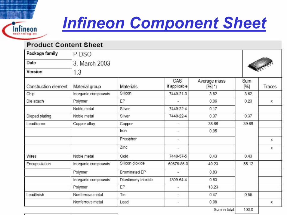
Infineon Component Sheet

/ Folie 8
Electronic Components Division JIC Hongkong 2004
Speed constantly Speed constantly increases
Metal-Industries
dDe
cl
-Gase
Recycling-Strat.
Electro Industrie
Target of national and european legislation ?? Chemical-Industry
Car-Industry
Eco-Design EUP
Ecolabel
WEEE/ROS
?? Ressource-Strat
ELV
EU-chemical polic
Green Std.
IPP
Electro(nic)-Industry
Target Electro(nic) Industrie ??? (!)
F
Env
P
y
ro
increases

/ Folie 9
Electronic Components Division JIC Hongkong 2004
Legislation - ELV (2000/53/EC)
End of Life Vehicles Directive (ELV) - 2000/53/EC , Annex II amended by 2002/525/EC
Current status: EnforcedSubstance bans in force since July 1st, 2003
Problems:Maximum concentration values (MCV) are related to „homogeneous material“ and „not intentionally added“.The definition is impractical in case of electronic assemblies and components; consequence: no implementation measures and marketsurveillance tools for those products are in force at member states up to now. IMDS entries are used as „proof“.

IPC Solder Products Value Council (SPVC)
• Management council formed in August 2001 by the leadership of the global solder manufacturing industry.
Goal of creating programs to benefit both solder manufacturers and their customers.
• Subcommittees: – Lead Free - Patents– Market Research - Environment– Industry Awareness

IPC SPVC Lead Free ResearchMembers
Aim, Inc.Amtech, Inc.AvantecCookson Electronics Assembly MaterialsEFD, Inc.HarimatecHenkel TechnologiesHeraeus, Inc.
Indium CorporationKester SolderKoki CompanyNihon SuperiorP. Kay Metals, Inc.Qualitek Int., Inc.Senju Metal IndustryShenmao Tech.Thai Solder

Lead Free Subcommittee
• Today, several consortia exist that are promoting various alloys to the electronics industry.
• The goal of the SPVC lead-free subcommittee is to reduce the confusion regarding alloy choice and is devoted to achieving a worldwide consensus on the issue.
• It is not the goal of the subcommittee to “invent” an alloy. Rather, the subcommittee is collecting all available data and will make a suggestion based upon the technical merit of the alloy.

C O
R P
O R
A T
E
T E
C H
N O
L O G
Y
© Siemens AG, CT MM 6, Gamalski, 04/2004H/Daten/IEC_Pb-frei_2.ppt
Materials &MicrosystemsPackaging &Assembly
DIRECTIVE 2002/…./EC OF THE EUROPEAN PARLIAMENT AND OF THE COUNCIL of/on waste electrical and electronic equipment (WEEE), 2000/0159 (COD); C5-0487/2002; PE-CONS 3662/02; Brüssel 8. November 2002
Categories of electrical and electronic equipment
covered by this Directive
1. Large household appliances
2. Small household appliances
3. IT and telecommunications equipment
4. Consumer equipment
5. Lighting equipment
6. Electrical and electronic tools (with the exception of large -sca le stationary
industrial tools)
7. Toy s, leisure and sports equipment
8. Medical devices (with the exception of all implanted and infected products)
9. Monitoring and control instruments
10. Automatic dispensers

C O
R P
O R
A T
E
T E
C H
N O
L O G
Y
© Siemens AG, CT MM 6, Gamalski, 04/2004H/Daten/IEC_Pb-frei_2.ppt
Materials &MicrosystemsPackaging &Assembly
Considerations for the Usage of Lead-free Solders
Pad-Metallisation ofSubstrate (e.g. PCB)
Metallization of ComponentsTermination / Composition of Solder
Bumps (BGA/CSP) 1)
Lead-free Solders for Wave-Reflow- and Rework Soldering
Parameters for SolderingProcess in Manufacturing
Reliability of Electronic Assemblies (First- und Second-Level)
Electrical Functionof the Components
Metallurgy of Solder Joints
Mechanical Propertiesof Solder Joints
1) Dependent onSupplier

C O
R P
O R
A T
E
T E
C H
N O
L O G
Y
© Siemens AG, CT MM 6, Gamalski, 04/2004H/Daten/IEC_Pb-frei_2.ppt
Materials &MicrosystemsPackaging &Assembly
Lead-free Solder - Alloys
Low-melting Pb-free solders
SnIn52118°C
SnBi58138°C
SnZn9199°C
High-melting Pb-free solders
SnCu0,7227°C
SnAg3,5221°C
SnAg3,8Cu0,7217°C
SnPbtoxic
SnPb37;183°C
SnBiSnIn SnZn SnCuSnAgCu SnAg
High cost (In),
limited resources
Low temp.ability
Low-meltingphases
TS = 96°C
Corrosion
-
No problems with corrosionbetter electr. + therm. conductivity than SnPbrelative cheap, lower density than SnPb
no influence of Pb expected
higher melting point related to SnPb

C O
R P
O R
A T
E
T E
C H
N O
L O G
Y
© Siemens AG, CT MM 6, Gamalski, 04/2004H/Daten/IEC_Pb-frei_2.ppt
Materials &MicrosystemsPackaging &Assembly
Datenmaterial Pb-freie Lote
Anspruch an breitere, universitäre Forschung zur Schliessung der Wissens-lücken grundlegender metallurgischer, physikalisch/chemischer EigenschaftenSAC im globalen Massstab (u. a. AIF / DVS – Unterstützung universitärerForschung; Initiativprogramm)
Database for Solder Properties with Emphasis on New Lead-free Solders
National Institute of Standards and Technology
& Colorado School of Mines
Properties of Lead-Free Solders
Release 4.0
Dr. Thomas Siewert National Institute of Standards and Technology
Dr. Stephen Liu
Colorado School of Mines
Dr. David R. Smith National Institute of Standards and Technology
Mr. Juan Carlos Madeni
Colorado School of Mines
Colorado, February 11, 2002
Japan

C O
R P
O R
A T
E
T E
C H
N O
L O G
Y
© Siemens AG, CT MM 6, Gamalski, 04/2004H/Daten/IEC_Pb-frei_2.ppt
Materials &MicrosystemsPackaging &Assembly
Distribution of Purchase Volume for PCB – Assemblies
Total: 100%
IC´cConnectorsConsumable Mat.Power SuppliesPCB´sPassive Comp.Discrete Comp.
Costs for Consumable Materials: appr. 1% of the toal Purchase Volume !

C O
R P
O R
A T
E
T E
C H
N O
L O G
Y
© Siemens AG, CT MM 6, Gamalski, 04/2004H/Daten/IEC_Pb-frei_2.ppt
Materials &MicrosystemsPackaging &Assembly
Ag
Sn
Cu
3.5
7.7
1.0
4.0IOWA
Senju/Matsushita
0.5
3.03.0
5.0
SN96CI
0.021,5
0,01
1,5
Cookson
0.5
6,0
0,5
3,0
Oatey
SN97C
SnAg2,5Cu0,5Bi
SACX

Marking, Symbols and Labels for Identification of Lead-Free
and Other Reportable Materials in Lead-Free Assemblies, Components and Devices
April 21, 2004

Goals and Objectives
• Common terminology for marking schemes across the industry
Any solution must be global• Communicate materials of concern within
the supply chain• Support manufacturing, repair, and recycling• Not intended for RoHS border compliance• Maximum simplicity
Reduce the chances of producer and administrative quality errors
• Minimum size necessary Component labeling desired
• Manufacturability


IEC Advisory Committee on Environmental Aspects –
ACEA:
Work on test methods for absence of lead (& other
substances)

Project plan as proposed by ACEAin March 2004
...TCPublish the combined (or product-specific) standard n
2005-12WGProduce Committee Draft for Vote of the analytical standard8
2005-03WGProduce Committee Draft of the analytical standard7.
2004-11WGProduce Working Draft of the analytical standard6.
2004-06GB+Conv.Involve members of TCs in the analytical group5.
2004-05GB (RoHS text: UK)
Identify important TCs to take part: A = directly concerned by the RoHS categories; B = others involved; C = not involved
4.
2004-05MStutzConsolidate methods, ideas, collect all existing material contributing to the first draft
3.
GBarta,SMBCarry out consultations on procedure and TC to use for development and publication of analytical standard
2.
2004-04MStutz, GBartaSet up the group for the analytical part (incl. secretariat) — Convenor M.Stutz
1.
By whenWhoWhat

Importance for Setting Standard Testing Methods
Compliance checks have to be performed in a consistent and reliable manner
Need for detailed specifications of standard methods to verify with the regulations
Standard compliance methods need to be implementable by laboratories all around the world
International standard methods encourage trade of products by avoiding technical barriers
Harmonisation of compliance and enforcement methods is essential for a proper functioning of the global market

Scope of Standard Testing Method
The standard testing methods need to:Cover all RoHS substances (Pb, Hg, Cd, Cr VI, PBB, PBDE)Target electronic and electrical equipment (EEE), including components thereofAllow testing which is simple, fast, of high quality, and cost effective

Standard Testing Methods Content
Analytical methods (material dependent)Sample preparationAnalytical instrument definitionReference methods
Laboratory implementation: Including elements for:Quality assuranceProviding consistent resultsDocumentation[=> GLP and/or accreditation to (inter-)national systems (e.g. ISO)]

Standard RoHS Test ProcedurePBB/PBDE
Pb > 750 ppm
Cr > 750 ppmSamples
Homogenious Materials
MetalsPlastics
PWB/Components
Screening
EDXRF
RoHS Compliant
Br, Cr, Hg, Pb < 750 ppm
Cd < 75 ppm
Br > 750 ppm IR, HPLC
Diphenyl-carbazide Cr VI
Hg > 750 ppmHgAAS
EDXRF, ICP-AES Pb
Cd > 75 ppm EDXRF, ICP-AES Cd

Standard Testing Methods Depending on Material Type
None commercially available,
In-house references
Commercial Soild Metal Standards
None commercially available,
In-house references
References
EDXRF (Br, Sb)
ICP-AES (all other elements)
EDXRF (all elements heavier than Na)
Diphenylcarbazidemethod (Cr VIspeciation)
EDXRF (Pb, Br, Cr, Cd, Hg)
HPLC/UV (PBB, PBDE)
FT-IR (PBB, PBDE)
Diphenylcarbazide method (Cr VIspeciation)
Analytical instrument definition
Acid DigestionDirect measurement,
grinding
Direct measurement,
Powder measurement, thin foils
Sample preparation
PWBsMetalsPlastics
Shaded row: Most important testing standard

Standard RoHS Test Method Documentation
Sample Type and Sample Preparation
Test Instrumentation and
Operation
Result
Reference Samples
Reference Methods
Validation
Standard RoHS Test Method Documentation

International Standard Methods Status
DIN 38.414, EPA 3050B, EPA 3052: Digestion and determination of heavy metals in printed wiring boards
Form the development base for new standards developments for PWB sample preparation, instrument definition, and calibration
EN 1122:2001: Determination of Cd in plasticsForms the development base for new standards developments for plastic sample preparation, instrument definition, and calibration
NIST (National Institute of Standards, US) and, BCR (Community Bureau of Reference, EU): Traceable material references
Forms the development base for new standards developments for reference materials development

Review & Support for Testing Procedure and Processes
AeA (American Electronics Association) Meeting Phoenix (Feb 2004):15 US companies reviewed & supported testing procedure & process
USITO (US International Trade Organization):Presented to testing procedure & process Chinese Ministry (MII) for RoHS testing
EICTA/Orgalime/AeA Europe/JBCE:Reviewed testing procedure & process for submission to EU TAC for RoHS

JISSO Concept Definition
Interface and Solution technology betweenuser and suppliers for Interconnecting,assembling, packaging, mounting andintegrating system design.
- This contains both functional and physical technology.

JISSO Levels Concept
4-Electronic Unit
3-Electronic ModulePropertybeforeJisso
1-Electronic Element
2-Electronic PackageJisso Level0
JISSOProduct
Level
Functional and Physical State
4
JISSOInterface
Level
Functional State Physical
State
Electronic System
Jisso Level5
3
21
UserSuppliers

Definition of Basic Jisso Levels• Level 0 - Property before Jisso
– Includes standards, patents and proprietary methodology• Jisso Product Level 1 – Electronic Element
– Bare die/Wafer ready to be mounted, semi-finished component• Jisso Product Level 2 – Electronic Package
– Electronic, Optoelectronic, Mechanical MEMS, Includes finished components
• Jisso Product Level 3 – Electronic Module – Electronic, Optoelectronic, Mechanical MEMS
• Jisso Product Level 4 – Electronic Unit – Electronic, Optoelectronic, Mechanical MEMS
• Level 5 – Electronic System– Electronic, Optoelectronic, Mechanical, Backplane, Housing or
Cabling

Level 0 – Property before Jisso The intellectual property of an item pertains to the idea or intelligence imported or described in a formal document (protocol, standards and/or specifications), design entity or patent disclosure.-The information may be in hard or soft copy and can include computer code or data format as a part of the descriptive analysis.
-The characteristics are described as to their physical, chemical, electrical, mechanical, electromechanical, environmental, and/or hazardous properties.

Level 1 – Electronic Element
Uncased bare die or discrete components (resistor , capacitor, diode, transistor, inductor, fuse), with metallization or termination ready for mounting. -This can be an IC, or discrete electrical, optical or MEMS element. -Individual elements cannot be further reduced without destroying their stated function.

Level 2 – Electronic Package
A container for an Individual Electronic Element or Elements which protects the contents and provides terminals for making connections to the rest of the circuit. -The Package outline is generally standardized or meets guideline standards. -The Package may function as electronic, optoelectronic, or Micro-Electro-Mechanical-Systems, and may in the future include Bio-electronic sensors.

IC Component Package Examples
Single Die Package
Pyramid Stacked DiePackage
Same Size Stack Die Package

Jisso Level 2 - Electronic Packages
Exact description of products to be determined
For discussion and consideration-

Level 3 – Electronic Module
A sub-assembly with functional blocks which consist of Individual Electronic Elements and /or Component Packages.- An individual module having an application specific purpose including Electronic, Optoelectronic or Mechanical (MEMS).- The module generally provides protection of its elements and packages, depending on the application.

Jisso Level 3- Electronic Modules
Exact description of products to be determined
For discussion and consideration-

Electronic Module Categorized by Interface
Wired ModuleA module which has electrical interface(Current Majority)
Wireless ModuleA module which has wireless interface
Opto-electrical ModuleA module which has optical interface
Cyber-Gate ModuleA module which has transducer between real and virtual
world information
Sensor ModuleA module which can input real world information
Realizing ModuleA module which can output real world information

Module Registration by Function
Data Processing CPU ModuleCamera ModuleTV ModuleTelephone Module
Real world information I/OSensor ModuleDisplay Module
OtherCard Module
Power GeneratingPower ModuleVRM
High FrequencyRF ModuleVCO Module
Data StorageMemory Module
NetworkSwitching Module

MaterialDeclarationIssues