ma840 emilyedit - kollmorgen
TRANSCRIPT

MA840
PC840 Hardware & Software Reference Manual
Brushless Servo Drive with SERCOS Interface
203 West Rock RoadRadford, VA 24141
(540) 633-3545Fax (540) 639-4162
Part# MA840March, 2012
Rev B

This document is copyrighted by Kollmorgen. It issupplied to the user with the understanding that it will not bereproduced, duplicated, or disclosed in whole or in partwithout the express written permission of Kollmorgen.
Copyright © 2001

WARRANTY AND LIMITATION OF LIABILITY
Includes software provided by Kollmorgen
Kollmorgen warrants its motors and controllers ("Product(s)") to the originalpurchaser (the "Customer"), and in the case of original equipment manufacturers ordistributors, to their original consumer (the "Customer") to be free fromdefects inmaterial and workmanship and to be made in accordance with Customer'sspecifications which have been accepted in writing by Kollmorgen. In no event,however, shall Kollmorgen be liable or have any responsibility under such warrantyif the Products have been improperly stored, installed, used or maintained, or ifcustomer has permitted any unauthorized modifications, adjustments, and/orrepairs to such Products. Kollmorgen's obligation hereunder is limited solely torepairing or replacing (at its option), at its factory any Products, or parts thereof,which prove to Kollmorgen's satisfaction to be defective as a result of defectivematerials or workmanship, in accordance with Kollmorgen's stated warranty,provided, however, that written notice of claimed defects shall have been given toKollmorgen within two (2) years after the date of the product date code that isaffixed to the product, and within thirty (30) days from the date any such defect isfirst discovered. The products or parts claimed to be defective must be returned toKollmorgen, transportation prepaid by Customer, with written specifications of theclaimed defect. Evidence acceptable to Kollmorgen must be furnished that theclaimed defects were not caused by misuse, abuse, or neglect by anyone other thanKollmorgen.Kollmorgen also warrants that each of the Kollmorgen Motion Control SoftwarePrograms ("Program(s)") will, when delivered, conform to the specificationstherefore set forth in Kollmorgen's specifications manual. Customer, however,acknowledges that these Programs are of such complexity and that the Programsare used in such diverse equipment and operating environments that defectsunknown to Kollmorgen may be discovered only after the Programs have been usedby Customer. Customer agrees that as Kollmorgen's sole liability, and as Customer'ssole remedy, Kollmorgen will correct documented failures of the Programs toconform to Kollmorgen's specifications manual. KOLLMORGEN DOES NOTSEPARATELY WARRANT THE RESULTS OF ANY SUCH CORRECTIONOR WARRANT THAT ANY OR ALL FAILURES OR ERRORS WILL BECORRECTED OR WARRANT THAT THE FUNCTIONS CONTAINED INKOLLMOREN'S PROGRAMS WILL MEET CUSTOMER'S REQUIREMENTSOR WILL OPERATE IN THE COMBINATIONS SELECTED BYCUSTOMER. This warranty for Programs is contingent upon proper use of thePrograms and shall not apply to defects or failure due to: (i) accident, neglect, ormisuse; (ii) failure of Customer's equipment; (iii) the use of software or hardwarenot provided by Kollmorgen; (iv) unusual stress caused by Customer's equipment;or (v) any party other than Kollmorgen who modifies, adjusts, repairs, adds to,deletes from or services the Programs. This warranty for Programs is valid for aperiod of ninety (90) days from the date Kollmorgen first delivers the Programs toCustomer.
i

THE FOREGOING WARRANTIES ARE IN LIEU OF ALL OTHERWARRANTIES (EXCEPT AS TO TITLE), WHETHER EXPRESSED ORIMPLIED, INCLUDING WITHOUT LIMITATION, ANY WARRANTY OFMERCHANTABILITY OR OF FITNESS FOR ANY PARTICULARPURPOSE,AND ARE IN LIEU OF ALL OTHER OBLIGATIONS OR LIABILITIES ONTHE PART OF KOLLMORGEN. KOLLMORGEN MAXIMUM LIABILITYWITH RESPECT TO THESE WARRANTIES, ARISING FROM ANY CAUSEWHATSOEVER, INCLUDING WITHOUT LIMITATION, BREACH OFCONTRACT, NEGLIGENCE, STRICT LIABILITY, TORT, WARRANTY,PATENT OR COPYRIGHT INFRINGEMENT, SHALL NOT EXCEED THEPRICE SPECIFIED OF THE PRODUCTS OR PROGRAMS GIVING RISE TOTHE CLAIM, AND IN NO EVENT SHALL KOLLMORGEN BE LIABLEUNDER THESE WARRANTIES OR OTHERWISE, EVEN IFKOLLMORGEN HAS BEEN ADVISED OF THE POSSIBILITY OF SUCHDAMAGES, FOR SPECIAL, INCIDENTAL, OR CONSEQUENTIALDAMAGES, INCLUDING WITHOUT LIMITATION, DAMAGE OR LOSSRESULTING FROM INABILITY TO USE THE PRODUCTS ORPROGRAMS, INCREASED OPERATING COSTS RESULTING FROM ALOSS OF THE PRODUCTS OR PROGRAMS, LOSS OF ANTICIPATEDPROFITS, OR OTHER SPECIAL, INCIDENTAL, OR CONSEQUENTIALDAMAGES, WHETHER SIMILAR OR DISSIMILAR, OF ANY NATUREARISING OR RESULTING FROM THE PURCHASE, INSTALLATION,REMOVAL, REPAIR, OPERATION, USE OR BREAKDOWN OF THEPRODUCTS OR PROGRAMS, OR ANY OTHER CAUSE WHATSOEVER,INCLUDING NEGLIGENCE. The foregoing shall also apply to Products,Programs, or parts for the same which have been repaired or replaced pursuant tosuch warranty, and within the period of time, in accordance with Kollmorgen's dateof warranty. No person, including any agent, distributor, or representative ofKollmorgen, is authorized to make any representation or warranty on behalf ofKollmorgen concerning any Products or Programs manufactured by Kollmorgen,except to refer purchasers to this warranty.
ii

Table of Contents.....................................................
1 Overview of the PC840 1-1
1.1 Interfaces and Connections 1-11.2 Setting up Intensity and Baud Rate using SW4 1-31.3 Seting up Serial Addresses Using SW5 and SW6 1-41.4 Identification Numbers 1-6
2 Interfaces and Connections 2-1
2.1 Power Connector (TB1) 2-12.2 Serial Port (J1) 2-42.3 Command I/O (J2) 2-82.4 Feedback (J3) 2-26
3 Inputs/Outputs 3-1
3.1 General Purpose I/O 3-13.2 Probe/Registration Functionality 3-123.3 Analog Input 3-133.4 Analog Outputs 3-133.5 DACMap Parameters 3-15
4 Servo Loop Parameters 4-1
4.1 Current Loop 4-14.2 Velocity Loop 4-14.3 Position Loop 4-104.4 Advanced Velocity Loop Tuning 4-15
5 IDN Attributes 5-1
5.1 SERCOS Specific Parameters 5-15.2 Manufacturer Specific Parameters 5-58
MA840 Rev 1

6 Protection Circuits and Diagnostics 6-1
6.1 Troubleshooting 6-56.2 Motor Commutation 6-66.3 System Protection 6-9
Appendix A - Specifications A-1
Appendix B - Ordering Information B-1
Rev 1 MA840

1 Overview of the PC840
Introduction This chapter introduces the PC840 SERCOS drive. Topicscovered are:
• PC840 Overview
• PC840 Connection Diagram
• Setting Intensity and Baud Rate using SW4
• Setting up Serial Address Using Rotary Switches SW5and SW6
• List of Supported IDNs
PC840 overview The PC840 SERCOS contains all the hardware and firmwarenecessary to connect to a SERCOS network.
This chapter explains how to wire a PC840 system, definesswitch settings, and lists the SERCOS IDNs the PC840supports.
1.1 Interfaces and Connections
Introduction The diagrams on the following pages show the connections forinputs and outputs for the PC840.
• Power Board 13-Position Terminal Strip
• RS-232 Serial Port 9-pin female D-connector
• Command I/O 44-pin female D-connector
• Fiber Optic Transmit and Receive connectors
MA840 - Rev 1 1 - 1

PC840connectiondiagram
1 - 2 MA840 - Rev 1
RS
-232
/485
1 2 3 4 5 6 7 8 9
AN
ALO
GC
MD
+A
NA
LOG
CM
D-
COMMANDI/O
AN
ALO
GO
UT
PU
T2
(DA
CM
ON
ITO
R2)
SY
ST
EM
STA
TU
SM
ON
ITO
RIN
GA
NA
LOG
CU
RR
EN
TLI
MIT
LIM
ITS
WIT
CH
EX
AM
PLE
+24
VD
CU
SE
RS
UP
PLY
EN
CO
DE
RO
UT
PU
TC
HA
NN
EL
Z
PC
840
J2
I/OR
TN
EN
CO
DE
RO
UT
PU
TC
HA
NN
EL
Z
PE
CH
AS
SIS
GR
OU
ND
PO
INT
TB
1 ACPOWER
654321F
RO
MO
TH
ER
ELE
CT
RO
NIC
S
L2C
TR
LV
AC
L1C
TR
LV
AC
26N
OC
ON
NE
CT
RE
LAY
OU
TP
UT
(-)
(OU
T4)
2524232220E
NC
OD
ER
INP
UT
CH
B(D
IR)
EN
CO
DE
RIN
PU
TC
HB
(DIR
)E
NC
OD
ER
INP
UT
CH
A(S
TE
P)
INC
RE
ME
NTA
LS
HA
FT
PO
SIT
ION
OU
TP
UT
INC
RE
ME
NTA
LP
OS
ITIO
NC
OM
MA
ND
I/OR
TN
AN
ALO
GO
UT
PU
T1
(DA
CM
ON
ITO
R1)
EN
CO
DE
RO
UT
PU
TC
HA
NN
EL
AE
NC
OD
ER
OU
TP
UT
CH
AN
NE
LA
L124
0V
AC
L224
0/12
0V
AC
L324
0/12
0V
AC
+5
VD
C(O
UT
PU
T,25
0m
A)
I/OR
TN
/+
5V
DC
RT
NI/O
RT
NE
NC
OD
ER
INP
UT
CH
A(S
TE
P)
NO
CO
NN
EC
TN
OC
ON
NE
CT
NO
CO
NN
EC
TR
ELA
YO
UT
PU
T(+
)(O
UT
4)
12 2111 13 19181716151410E
NC
OD
ER
OU
TP
UT
CH
AN
NE
LB
EN
CO
DE
RO
UT
PU
TC
HA
NN
EL
B
12
34
56
78
9
SHIELD/+5 VDC RTN
+5 VDC
I/O RTN/+5 VDC RTN
TO
HO
ST
SE
TU
PO
RC
ON
TR
OL
CO
MP
UT
ER
SE
RIA
LPO
RT
J1
47-
63H
z
240/
120
VA
C
7 8 9
REGEN
-B
US
RE
GE
NR
+B
US
RE
SO
LVE
R
PTC
PTC
RT
N
+5V
DC
I/OR
TN
EN
CO
DE
RIN
PU
TC
HA
NN
EL
A(+
)
EN
CO
DE
RIN
PU
TC
HA
NN
EL
A(-
)
EN
CO
DE
RIN
PU
TC
HA
NN
EL
B(+
)
EN
CO
DE
RIN
PU
TC
HA
NN
EL
B(-
)
1 2 3 4 5 6 7 8 9
J3
POWERMOTOR
13121110C
HA
SS
ISG
ND
PH
AS
EU
PH
AS
EV
PH
AS
EW
MO
TO
R
FEEDBACKR
1E
XC
IT
R2
EX
CIT
RT
N
S1
/H
ALL
1
S3
/H
ALL
2
S2
/H
ALL
3
S4
PAC
IFIC
SC
IEN
TIF
ICB
RU
SH
LES
SM
OT
OR
PT
C
RS-232 TXD
RS-232 RXD
RS-485 TXD +
RS-485 TXD -
RS-485 RXD +
RS-485 RXD -
13121110 1514
I/OR
TN
AN
ALO
GIN
PU
T3
37E
NA
BLE
INP
UT
INP
UT
6IN
PU
T5
(RE
G2)
INP
UT
1(F
AU
LTR
ES
ET
)IN
PU
T2
(CW
INH
)IN
PU
T3
(CC
WIN
H)
INP
UT
4(R
EG
1)
2928 30 36353433323127N
OC
ON
NE
CT
AN
ALO
GIN
PU
T2
44O
UT
3O
UT
2(
)B
RA
KE
OU
T1
()
FAU
LT
INP
UT
RT
N+
24V
DC
OU
TP
UT
RT
N+
24V
DC
(OU
TP
UT,
80m
A)
OU
T1,
2,3
SU
PP
LY(I
NP
UT
)
434241403938
+ -
PE
12.5
EX
TER
NA
LΩ
RX
TXSERCOS
OUT
SERCOSIN

1.2 Setting up Intensity and Baud Rate Using SW4
Definition Switch SW4 is used to select the SERCOS baud rate and thefiber optic light intensity (power level).
Switch SW4 The following diagram shows the location of switch S4.
Intensity Level
SW4-1 Fiber Optic Light Intensity Level
ON High power transmission
OFF Low power transmission (default)
Baud Rate
Baud Rate SW4-2 SW4-3
2 Mbaud (default) OFF OFF
4 MBaud OFF ON
8 MBaud ON OFF
16 MBaud ON ON
MA840 - Rev 1 1 - 3
12
3O N

1.3 Setting up Serial Addresses Using Switches SW5 andSW6
Definition The two hexademical rotary switches SW5 and SW6 are usedto set the axis address for each PC840 on the SERCOS ring.
Procedure The following diagram shows the location of switch SW5 andSW6. The view shows the location of the switches looking atthe front of the PC840.
Note: Each PC840 must have a unique serial address.
Switch SW5 andSW6
The diagram below shows the SW5 and SW6 switch settings.
The 8-bit address consists of two hexadecimal digits. The lowand high digits are determined by the position of SW5 andSW6.
Note: The axis address is set to 1 by default at the factory.
1 - 4 MA840 - Rev 1
01234
56789AB
CD
EF
01234
56789AB
CD
EF

Procedure 1. Remove power from the PC840 servocontroller.
2. Refer to the table below to set the PC840 to theappropriate address.
Address table
Address SW6 SW5 Address SW6 SW5
0* 0 0 18 1 2
1 0 1 19 1 3
2 0 2 20 1 4
3 0 3 21 1 5
4 0 4 22 1 6
5 0 5 23 1 7
6 0 6 24 1 8
7 0 7 25 1 9
8 0 8 26 1 A
9 0 9 27 1 B
10 0 A 28 1 C
11 0 B 29 1 D
12 0 C 30 1 E
13 0 D 31 1 F
14 0 E 32 2 0
15 0 F … … …
16 1 0 … … …
17 1 1 255** F F
*Repeater Application Only**Not Allowed for SERCOS Applications
3. Re-connect power to the PC840.
4. Repeat steps 1 through 4 for other units on the ring.Make sure to give the other units unique addresses.
MA840 - Rev 1 1 - 5

1.4 Identification Numbers (IDNs)
Introduction This is the list of SERCOS IDNs which are supported by thePC840. For additional information on each IDN pleaseconsult a SERCOS specification or Chapter 6.
List of supportedIDNs
1 Control Unit Cycle Time (TNcvc)
2 Communication Cycle Time (Tscvc)
3 Shortest AT Transmission Starting Time (T1min)
4 Transmit/Receive Transition Time (TATMT)
5 Minimum Feedback Processing Time (T4min)
6 AT Transmission Starting Time (T1)
7 Feedback Acquisition Capture Point (T4)
8 Command Value Valid Time (T3)
9 Position of Data Record in MDT
10 Length of Master Data Telegram
11 Class 1 Diagnostic
14 Interface Status
15 Telegram Type Parameter
16 Configuration List of AT
17 IDN List of all Operation Data
18 IDN List of Operation Data for CP2
19 IDN List of Operation Data for CP3
21 IDN List of Invalid Operation Data for CP2
22 IDN List of Invalid Operation Data for CP3
24 Configuration List of the MDT
25 IDN List of all Procedure Commands
28 MST Error Counter
1 - 6 MA840 - Rev 1
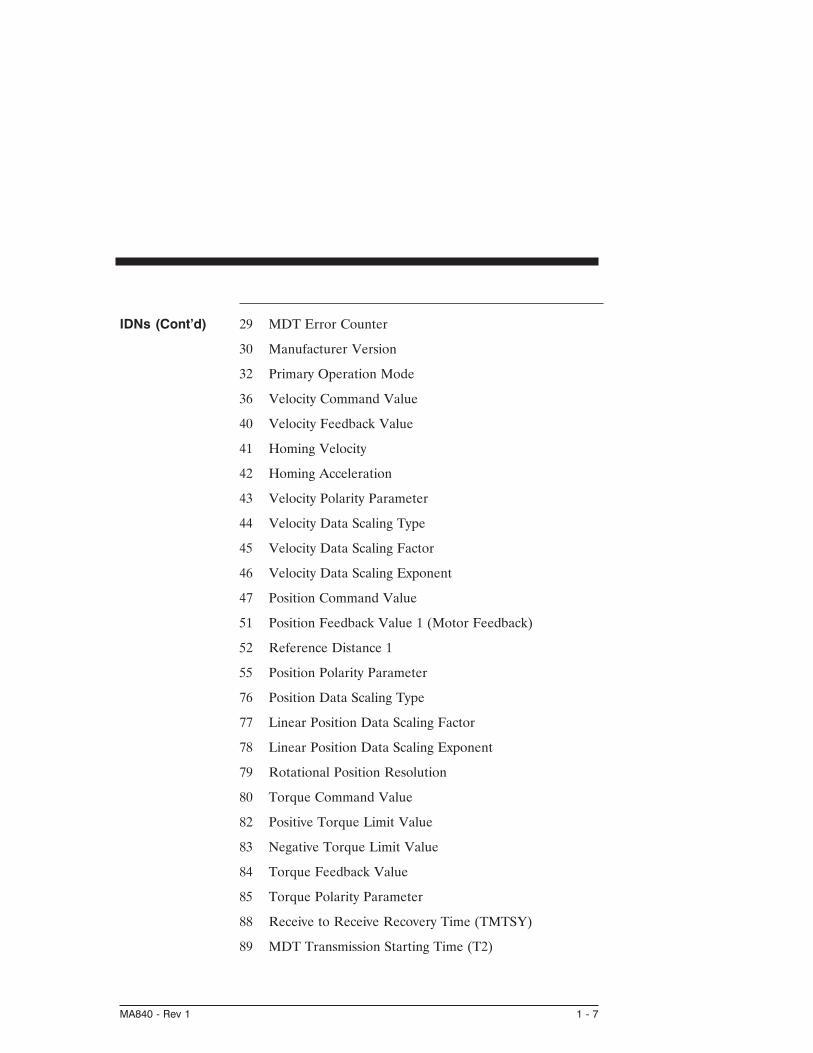
IDNs (Cont’d) 29 MDT Error Counter
30 Manufacturer Version
32 Primary Operation Mode
36 Velocity Command Value
40 Velocity Feedback Value
41 Homing Velocity
42 Homing Acceleration
43 Velocity Polarity Parameter
44 Velocity Data Scaling Type
45 Velocity Data Scaling Factor
46 Velocity Data Scaling Exponent
47 Position Command Value
51 Position Feedback Value 1 (Motor Feedback)
52 Reference Distance 1
55 Position Polarity Parameter
76 Position Data Scaling Type
77 Linear Position Data Scaling Factor
78 Linear Position Data Scaling Exponent
79 Rotational Position Resolution
80 Torque Command Value
82 Positive Torque Limit Value
83 Negative Torque Limit Value
84 Torque Feedback Value
85 Torque Polarity Parameter
88 Receive to Receive Recovery Time (TMTSY)
89 MDT Transmission Starting Time (T2)
MA840 - Rev 1 1 - 7

IDNs (Cont’d) 90 Command Value Proceeding Time (TMTSG)
95 Diagnostic Message
96 Slave Arrangement
99 Reset Class 1 Diagnostic
100 Velocity Loop Proportional Gain (kvp)
101 Velocity Loop Integral Action Time (kvi)
103 Modulo Value
104 Position Loop Kv Factor (kpp)
106 Current Loop Proportional Gain 1 (kip)
107 Current Loop Integral Action Time 1 (kii)
110 Amplifier Peak Current
127 Communications Phase 3 Transition Check
128 Communications Phase 4 Transition Check
129 Manufacturer Class 1 Diagnostic
130 Probe Value 1 Positive Edge
131 Probe Value 1 Negative Edge
132 Probe Value 2 Positive Edge
133 Probe Value 2 Negative Edge
140 Controller Type
142 Application Type
143 SYSTEM Interface Version
147 Homing Parameter
148 Drive-Controlled Homing Procedure Command
159 Monitoring Window
160 Acceleration Data Scaling Type
161 Acceleration Data Scaling Factor
1 - 8 MA840 - Rev 1

IDNs (Cont’d) 162 Acceleration Data Scaling Exponent
169 Probe Control Parameter
170 Probing Cycle Procedure Command
185 Length of the Configurable Data Record in the AT
186 Length of the Configurable Data Record in the MDT
187 IDN List of Configurable data in the AT
188 IDN List of Configurable data in the MDT
189 Following Distance (PosErrorMax)
192 IDN List of Backup Operation Data
263 Load Working Memory Procedure Command
264 Backup Working Memory Procedure Command
301 Allocation of Real-Time Control Bit 1
303 Allocation of Real-Time Control Bit 2
305 Allocation of Real-Time Status Bit 1
307 Allocation of Real-Time Status Bit 2
400 Home Switch
401 Probe 1
402 Probe 2
403 Position Feedback Value Status
405 Probe 1 Enable
406 Probe 2 Enable
409 Probe 1 Positive Latched
410 Probe 1 Negative Latched
411 Probe 2 Positive Latched
412 Probe 2 Negative Latched
MA840 - Rev 1 1 - 9

IDNs (Cont’d) 32800 DSP Debug Address
32801 DSP Debug Word
32802 DSP Debug Dword
32803-32806 ARM Debug Variables
32807 Pole Count
32809 Filter Value for ADF0
32810 DM1F0
32811 DM2F0
32812 DM1Gain
32813 DM2Gain
32814 DM1Map - Mux Select
32815 DM2Map - Mux Select
32816 EncOut (Encoder Output)
32817 InpMap1
32818 InpMap2
32819 InpMap3
32820 InpMap4
32821 InpMap5
32822 InpMap6
32823 EncInFilt
32824 RemoteFB
32826 CommOff
32828 EncIn (Encoder Input)
32829 ITThresh
32830 StopTime
32831 VBusThresh
1 - 10 MA840 - Rev 1

IDNs (cont’d) 32832 VelLmtHi
32833 VelLmtLo
32835 CoastTime
32836 CommEnbl
32837 Motor 1 Name
32838 Motor 2 Name
32840 Kvff
32841 ARZ0
32842 ARZ1
32843 ARF0
32844 ARF1
32845 Firmware version
32846 Encoder Data Scaling Method
32847 Encoder Modulo Value
32853 CommSrc (Commutation Source)
32857 ResPos (Resolver Position)
32858 Last Fault
32859 Last ExtFault
32860 OutMap1
32861 OutMap2
32862 OutMap3
32863 OutMap4
32866 Analog Input Voltage Offset (ADOffset)
32870 I2*t Motor Protection Threshold Value (I^2*tFilt)
32871 I2*t Motor Protection Low Pass Filter Value (I^2tF0)
32872 I2*t Motor Current Value
MA840 - Rev 1 1 - 11

IDNs (cont’d) 32875 State of Hall Sensors (HallState)
32876 Offset Angle for Hall Sensors (HallOffset)
32878 Digital Command Counts (DigitalCmd)
32879 Digital Command Frequency (DigitalCmdFreq)
32880 AnalogOut1
32881 AnalogOut2
32882 Analog Current Limit Value (AnalogILmt)
32883 Analog Current Limit Gain (AnalogILmtGain)
32884 Analog Current Limit Filter (AnalogILmtFilt)
32885 Analog Current Limit Offset (AnalogILmtOffset)
32886 Actual Positive Current Limit (ActualILmtPlus)
32887 Actual Negative Current Limit (ActualILmtMinus)
34817 PC840 Input Bit #1
34818 PC840 Input Bit #2
34819 PC840 Input Bit #3
34820 PC840 Input Bit #4
34821 PC840 Input Bit #5
34822 PC840 Input Bit #6
34824 PC840 Input Port (Inputs)
34825 AnalogIn
34826 EncPos (Encoder Position)
34833 PC840 Output Bit #1
34834 PC840 Output Bit #2
34835 PC840 Output Bit #3
34836 PC840 Output Bit #4
34840 PC840 Output Port (Outputs)
1 - 12 MA840 - Rev 1

2 Interfaces and Connections
Introduction This chapter describes all of the connections to the PC840and provides the information required to interface to it.
In the list below an overbar on a signal name means that thesignal is active low logic. For example, “Fault” indicates thedrive is faulted when it is pulled low.
Earth Ground Chassis Ground, M4 x 12 screw with flat and lock washer.
2.1 PC840 Power Board Connector
TB1 13 Position Terminal Strip
Pin Label Description
TB1-1 L1 240/120 VAC Control Power
TB1-2 L2 240/120 VAC Control Power
TB1-3 PE Chassis Ground
TB1-4 L1 240/120 VAC (Input)
TB1-5 L2 240/120 VAC (Input)
TB1-6 L3 240/120 VAC (Input)
TB1-7 +B + Bus
TB1-8 R Regen Transistor
TB1-9 -B - Bus
TB1-10 PE Chassis Ground
TB1-11 U Motor Phase U
TB1-12 V Motor Phase V
TB1-13 W Motor Phase W
MA840 - Rev 1 2 - 1

AC Power
L1, L2 (TB1-1, 2)240 VAC/ 120 VACControl Power
These terminals connect the 240/120 VAC power provided bythe user to the drive’s control voltage power supply.
If a single supply is used for bus power and control power,externally connect control L1, L2 (TB1-1, 2) to bus power L1,L2 (TB1-4, 5). Control power L1, L2 are NOT connectedinternally to bus power L1, L2.
Note: The control voltage for the PC840 controllers is input to aswitching power supply. This input will accept voltages rangingfrom 85 to 265 Vac.
Chassis Ground
PE (TB1-3) Convenience connector point for the user to connect thedrive’s control power and bus power to protective earthground. This pin is directly connected to the chassis and thusto the Chassis Ground Stud. Local electrical code may requireusing the Earth Ground Chassis stud for this function.
AC Power
L1, L2, L3(TB1-4, 5, 6)240 VAC/ 120 VAC
These terminals connect the 240/120 VAC power provided bythe user to the drive’s power output stage bus to drive themotor. For single phase operation use any two of theseterminals and leave the third terminal open.
RegenerationInterface
+B, R, -B(TB1-7, 8, 9)+Bus, RegenResistor, - Bus
These terminals provide the connection points for an externalresistor to absorb regenerated energy from the motor. Anexternal regeneration resistor goes from + B to R. -Bus (-B)on TB1-9 is usually left open.
Caution! High Voltage!
During normal operation +B, R, and -B operate at the bus powervoltages. A 240 Vac system operates at ≅ 400 Vdc. These aredangerous voltages.
2 - 2 MA840 - Rev 1

External RegenResistor
The table below lists the recommended values for an externalregen resistor. To order from Pacific Scientific use partnumber PRK-200.
Note: Regen Resistance MUST be in the range of 11.25 Ω to13.75 Ω.
Model Resistance
PC8x2/3/4 12.5 Ω ( ±10%), 200 W, 1,500 V Isolation
For safety it is recommended that the resistor be mounted ona grounded panel or use a grounding wire connected to amounting screw. The terminals of the resistor must not begrounded.
Warning!
Wait 10 minutes after Bus Power is removed for the bus capvoltage to decay to a safe level before touching regen resistor orwiring. The voltage on the bus caps can be monitored with avoltmeter from +BUS (TB1-7) to -BUS (TB1-9).
Motor Power
PE (TB1-10)Motor CaseGround
This termination provides a convenient point for the motorground connection and motor power wire shield. Localelectrical code may require using the Earth Ground Chassisstud for this function.
U, V, W(TB1-11, 12, 13)Motor Phase
These three terminations provide the 3-phase power output tothe brushless motor. Observe motor polarity on theseconnections. For example, connect U on the drive to U onthe motor.
MA840 - Rev 1 2 - 3

2.2 Serial Port
J1 The serial port (J1), utilizes the 9 contact female Dsubminiature style connector shown below. A brief descriptionof each signal is included in the J1 I/O table on following page.For additional information, please refer to the SerialCommunications Transceiver Schematic at the end of thissection.
J1 Diagram The figure below illustrates the pin-out for the 9 pinconnector. It shows the front view looking at the PC840.
2 - 4 MA840 - Rev 1
6
7
8
9
1
2
3
4
5

I/O Table
PinNumber
Input/Output Explanation
J1-1 Shield Common/shield - serial port interface
J1-2 RS-232 TXD RS-232 transmitter output (from PC840)
J1-3 RS-232 RXD RS-232 receiver input (to PC840)
J1-4 Not Used
J1-5 I/O RTN/+5 VDC RTN Common serial port interface
J1-6 Not Used
J1-7 Not Used
J1-8 Not Used
J1-9 Not Used
The information provided in this section should be used toconnect the PC840 to your computer for firmware upgrades.
MA840 - Rev 1 2 - 5

2.2.1 RS-232 Connections
RS-232Connections
RS-232 connections on J1 are shown below. Cable wiringrequired for connecting to either 9 or 25 pin serial ports ofmost computers are also shown.
Note: Pinouts vary among computer manufacturers. Check thehardware reference manual for your machine before wiring.
Cablingdiagram
A 6 foot (1.8 m) RS-232 Cable with 9 pin connectors and a 9pin to 25 pin adapter is available from Pacific Scientific. ThePacific Scientific order number is RS-232-5600.
Note: Shielded wiring is recommended for the serialcommunications cable to minimize potential errors from electricalnoise.
2 - 6 MA840 - Rev 1
I/O RTN
RS-232 RXD
RS-232 TXD
9 CONTACT FEMALE D SUBMINIATURE CONNECTOR
TYPICAL CABLES
9 PIN FEMALE
25 PIN FEMALE
9 PIN MALE
9 PIN MALE
TO PC(9 PIN)
TO PC(25 PIN)
TO PC830 J1
TO PC830 J1
3 2
2 2
2 3
3 3
7 5
5 5

PC840 SerialCommunicationsTransceiverSchematic
MA840 - Rev 1 2 - 7
J12 RS-232 TXD
SN75155
SN75155
75176
75176
332
332
2.21 K
2.21 K
46.4 K
46.4 K
2200pF
2200pF
+5 V
+5 V
1000pF
1000pF
6 RS-485 TXD+
7 RS-485 TXD-
TXD
RXD
TO UART
RS-485ENABLE
1 SHIELD
5 I/O RTN
4 +5 VDC
3 RS-232 RXD
8 RS-485 RXD+
9 RS-485 RXD-

2.3 Command I/O
J2 44 Position D subminiature female
Pin Description Pin Description
J2-1 Analog Command Input (+) J2-23 No Connect
J2-2 Analog Command Input (-) J2-24 Relay Output (+) (Out4)
J2-3 I/O RTN J2-25 Relay Output (-) (Out4)
J2-4 Analog Output1 (DacMonitor1) J2-26 No Connect
J2-5 Analog Output2 (DacMonitor2) J2-27 No Connect
J2-6 Analog Current Limit Input J2-28 Analog Input 2
J2-7 I/O RTN J2-29 Analog Input 3
J2-8 Encoder Output Channel A J2-30 I/O RTN
J2-9 Encoder Output Channel A J2-31 Input 1 (Fault Reset)
J2-10 Encoder Output Channel B J2-32 Input 2 (CwInh)
J2-11 Encoder Output Channel B J2-33 Input 3 (CcwInh)
J2-12 Encoder Output Channel Z J2-34 Input 4 (Reg1)
J2-13 Encoder Output Channel Z J2-35 Input 5 (Reg2)
J2-14 +5 VDC (Output) J2-36 Input 6
J2-15 I/O RTN/ +5 VDC RTN J2-37 Enable Input
J2-16 I/O RTN J2-38 Input RTN
J2-17 Command Encoder InputChannel A (Step)
J2-39 +24 VDC Output RTN
J2-18 Command Encoder InputChannel A (Step)
J2-40 +24 VDC (Output)
J2-19 Command Encoder InputChannel B (Dir)
J2-41 Out1, 2, 3 Supply (Input)
J2-20 Command Encoder InputChannel B (Dir)
J2-42 Out1 (Fault)
J2-21 No Connect J2-43 Out2 (Brake)
J2-22 No Connect J2-44 Out3
2 - 8 MA840 - Rev 1

J2 Diagram The figure below illustrates the pin-out for the 44 pinconnector. It shows the front view looking at the PC840.
MA840 - Rev 1 2 - 9
1
1530
44
1631

Command I/O
Analog CMD(+), (-) InputsJ2-1, 2
These inputs accept the analog command from the user. Thisis a differential input to an A/D. It has a maximum singleended input range with respect to I/O RTN on either input of± 21V and an input impedance of 50kΩ. The full scaledifferential command input range is ± 13.5 V. The offset andsingle pole low pass bandwidth of this signal is adjustable via asoftware setup parameter. When used as a motion commandthe gain from this input is also adjustable via a software setupparameter.
Note: Always connect I/O RTN (J2-3) to the signal ground of thesource. Failure to do so may result in erratic operation.
I/O RTNJ2-3, 7, 15, 16
This terminal is signal common for the analog andnon-optically isolated digital inputs and outputs. These pinsare internally connected in the drive.
For protection against line surges, one of the I/O RTN pinsmust be connected to Earth ground. Pacific Scientificrecommends making this connection at an earth ground pointin the cabinet reserved for single point grounding of all I/OReturns (drives and supplies).
2 - 10 MA840 - Rev 1
33.2K22.1K
0.01 Fµ
0.01 Fµ
22.1K33.2K
33.2K
33.2K
+12V
-12V
TL082J2-1
± 13.5VFULL SCALE
ANALOGCMD+
I/O RTN
ANALOGCMD-
J2-2
1200 Hz FILTER
TO A/D
IN DSP
AnalogIn
J2-3

Command I/O Continued
DAC Monitor1, 2 OutputsJ2-4, 5
These analog outputs are general purpose monitor points.The output range is ± 5.5 V with a resolution of 11V/65536 =0.168 mV. The source impedance is 1 kΩ, which yields amaximum short circuit to I/O RTN current of ± 5 mA. Theseoutputs are updated every 250 µS. There is a 2.5 kHz, 4.8 kHzand a 9.6 kHz analog Low Pass Filter on these outputs.
Each DAC MONITOR can be mapped by software to be oneof a number of internal variables. The scale factor and thefrequency of a single low pass filter pole are softwareadjustable on each output by the DM1Gain, DM1F0 andDM2Gain, DM2F0 software parameters for DAC Monitor 1and 2 respectively. Variables marked with a “∗” are not rangeclamped and are allowed to wrap around when the signalexceeds the output dac’s voltage range. The other variableswill clamp at maximum when they exceed the analog voltagerange. The table on the following page lists the defined signalmappings.
DacMon
MA840 - Rev 1 2 - 11
15K
C1022200pF
0.047 Fµ0.1 Fµ
681DacMon1
J2-4332
3.32K
R194FROM
DAC
fc = 4.8 kHz
FULL SCALE = 5.5 V 0-pk
fc = 2.5 kHz and 9.6 kHz
+12V
-12V
TL082CD

Dac Monitor List Table
DMxMap Variable Description DAC Out Units(DMxGain = 1)
0 AnalogOutx Actual Analog Output Command V/V1 VelFB Measured Velocity (DM2 Default) 1 V/kRPM2 VelCmdA Actual Velocity Command (VelCmdA) 1 V/kRPM3 VelErr Velocity Error 1 V/kRPM4 FVelErr Compensated Velocity Error 1 V/kRPM5 Position Measured Position* 1 V/Rev6 PosError Position Error* 1 V/Rev7 PosCommand Commanded Position* 1 V/Rev8 Icmd Commanded Torque Current 1 V/A9 IFB Measured Torque Current (DM1 Default) 1 V/A10 AnalogIn Filtered A/D Input 1 V/V11 EncFreq Encoder Frequency 1 V/Hz12 EncPos Encoder Position* 10 V/4096 Cnts13 ItFilt Filtered Output Current Amplitude 1 V/100%14 HSTemp Measured Heat Sink Temperature 1 V/°C15 Commutation Electrical Angle* 1 V/Cycle16 IU Motor Phase U Output Current 1 V/A17 IV Motor Phase V Output Current 1 V/A18 IW Motor Phase W Output Current 1 V/A19 Motor Phase U Voltage Duty Cycle 1 V/100%20 Motor Phase V Voltage Duty Cycle 1 V/100%21 Motor Phase W Voltage Duty Cycle 1 V/100%22 VBus Drive Bus Voltage 1 V/V23 ResPos Resolver Absolute Position* 1 V/Rev24 Commanded non-torque current 1 V/A25 Measured non-torque current 1 V/A26 Torque Voltage Duty Cycle 1 V/100%27 Non-torque Voltage Duty Cycle 1 V/100%28 VelCmd Velocity Command (VelCmd) 1 V/kRPM29 DigitalCmdFreq Digital Command Frequency 1 V/Hz30 I^2*t I^2*t Filtered Current 1 V/%Ipeak^2
*These variables are allowed to wrap around when the signal exceeds the outputvoltage range.
2 - 12 MA840 - Rev 1

J2 Command I/O Continued
Analog CurrentLimit J2-6
This input limits the current flow to the motor when a voltageis applied with respect to I/O RTN.
CH A OUTCH A OUT,CH B Out,CH B OutOutputsJ2-8, 9, 10, 11
These two output pairs are differential TTL incrementalposition signals generated by the Resolver feedbackelectronics. These outputs are quadrature encoded to emulatean optical encoder. The resolution of these signals, i.e. theemulated line count, is set by the EncOut parameter. Theseoutputs are buffered by 26LS31 type RS-422 compatible linedrivers. Maximum recommended load current is ± 20 mA,which corresponds to a minimum line-to-line load resistanceof 100 Ω. This drive capacity corresponds to ten RS-422compatible inputs such as the PC830 encoder inputs. Theseoutputs are indefinitely short circuit proof to I/O RTN.
CH Z OUTCH Z OUTOutputsJ2-12, 13
These two terminals function as a differential, TTL markerpulse. The output pulse occurs once per motor shaftrevolution starting at resolver position = 0 and its width isapproximately one quadrature encoder width. This outputcomes from an 26LS31 type RS-422 compatible line driver.Maximum recommended load current is ± 20 mA, whichcorresponds to a minimum line-to-line load resistance of 100Ω. This drive capacity corresponds to ten RS-422 compatibleinputs such as the PC830 encoder inputs. This output isindefinitely short circuit proof to I/O RTN.
+5 VDC,I/O RTN/+5 VDCRTN OutputJ2-14, J2-15
These two connections provide an auxiliary power supply forthe user. This output is 5 Vdc ± 5% and is short circuitprotected at 1 A nominal. The maximum load limit for allconnections to this supply is 250 mA. The +5 VDC RTN(J2-15) is connected to I/O RTN (J2-3, J2-7, J2-16, J2-30).
MA840 - Rev 1 2 - 13

J2 Command I/O Continued
Encoder Inputs CH A IN, CH A IN, CH B IN, CH B IN,Step +, Step -, Dir +, Dir -,Step Up +, Step Up -, Step Dn +, Step Dn -
J2-17, 18, 19, 20 These inputs are used as a quadrature encoder, step anddirection, or up and down count format incremental signalsource. The decoding mode is set by the EncMode parameter.The scale factor of this incremental position command input isfully adjustable with software parameters. Full decoding speedor more noise immune slow speed decoding is softwareselectable.
These two input pairs are differential and are detected by26LS32 type RS-422 compatible line receivers. As differentialinputs, the recommended common mode range is <± 7 V withrespect to I/O RTN and the guaranteed differential voltagelogic thresholds are >± 0.2 V. Recommended drivers shouldbe able to source and sink > 3 mA to/from these inputs. Eachof these inputs have internal bias networks to allow easyconnection to single ended sources. When an input is opencircuited it will bias itself to between 2.2 and 2.5 V, thus theremaining input pair terminal will have a single endedguaranteed logic low for inputs < 2.0 V and a guaranteed logichigh for inputs > 2.7V. These levels are compatible with aTTL driver combined with a pull up resistor. Pull up resistorshould be < 470Ω.
2 - 14 MA840 - Rev 1

J2 Command I/O Continued
Relay OutputsJ2-24, 25
These relay outputs are normally open. They are rated for 1Amp at 30 VDC. These relays may be opened/closed byOut4. When the drive has no control power the relay is open.
Brake Output This output is low when the control power is off, or whencontrol voltage is on and the drive is disabled (Enabled = 0).This output is pulled high otherwise. This output is intendedto drive a normally open relay that in turn powers amechanical brake on the motor shaft for applications thatrequire a positive shaft lock when the servo drive is off.
MA840 - Rev 1 2 - 15
NormallyOpen
J2-24
J2-25

J2 Encoder I/O Interface Schematics Diagram
2 - 16 MA840 - Rev 1
ENCODER INPUTS
EMULATED ENCODER OUTPUTS
PC840 BASE UNIT ENCODER I/O
+5V
1K
1K
1K
1K
220pF
220pF
220pF
220pF
AM26LS32
AM26LS32
AM26LS31
AM26LS31
AM26LS31
J2-16
J2-13
J2-12
J2-11
J2-10
J2-9
J2-8
EMU A
EMU B
EMU Z
ENCIN A
CH B IN
CH A IN
CH A OUT
CH B OUT
CH Z OUT
I/O RTNCW ROTATION
CH A OUT
CH B OUT
CH Z OUT
I/O RTN
+5 VDC
CH A IN
CH B INENCIN B
+5V REG250 mA MAX
+8V UNREG
OPTION CARDUSER +5 VDC
RESOLVERPOSITIONTOEMULATEDQUADRATURE
PPR=EncOut
EncOut = 0PASSESENCIN A, BTO EMU A.B
TODECODE& COUNT
15K
15K
15K
15K
15K
15K
15KJ2-17
J2-18
J2-19
2.2 TO 2.5VOPEN CIRCUIT
J2-20
J2-14
J2-1615K

Using TTLdifferential linedrivers
MA840 - Rev 1 2 - 17
ENCODER PC840
+5V SUPPLY +5J2
14 +5 VDC @ 250 mA
CH A
CH B
I/O RTN
CH A
CH B
17
18TWISTEDPAIR
TWISTEDPAIR
19
20
16
CONNECT ONLY IF J2SOURCES ENCODER POWER
+5V SUPPLY
+5V SUPPLY RETURN
CH A
CH B

Using TTLsingle-endeddrivers
2 - 18 MA840 - Rev 1
ENCODER PC840
+5V SUPPLY +5J2
14 +5 VDC @ 250 mA
CH A
CH B
I/O RTN
CH A
CH B
17
18
TWISTEDPAIR
TWISTEDPAIR
19
20
16
CONNECT ONLY IF J2SOURCES ENCODER POWER
+5V SUPPLY
+5V SUPPLY RETURN
CH A
CH B

J2 Command I/O Continued
Auxiliary AnalogInputs J2-28, 29
Not Used.
Inputs 1-6 J2-31,32, 33, 34, 35, 36
These six optically isolated I/O connections are userprogrammable discrete 24 V inputs. These inputs share afloating return (J2-38) with the Enable Input (J2-37). Aminimum drive capability of 4 mA is required to fully powerthe opto. The user must supply 10 - 30 V to these inputs.
Note: 5 V inputs CAN NOT be used.
Each of the inputs is set and read by software every 2 mSec.Each one can be configured to be any of the availablefunctions and the configuration can be changed on the fly viadigital communications. The user’s default configuration isstored in the non-volatile memory. The present state of eachof these lines can be read via digital communications. Thelogic polarity of these signals is also software programmable.That is, an input can be defined to be active low or activehigh. For edge triggered functions the active edge isprogrammable.
Logic State InpX with respect to Input RTN
Low 0 to +2 V
Undefined +2 V to + 10 V
High +10 V to + 30 V
MA840 - Rev 1 2 - 19
J2-31
J2-38
INPUT
INPUT RTN
R2232.2K
R601K 1.1 V
+
MM
BD
914L
T1
-TLP121GB
TOCONTROLLOGIC
External10 - 30 V
+
-

J2 Command I/O Continued
The list below describes the subset of the available functionsand the mappings used as the factory defaults for each of theinputs.
Fault ResetInput
Input 1: This input is used to reset the amplifier following afault. This input is programmed active high so that an opencircuited input does not activate the function. During FaultReset active the output stage is disabled and the resetcondition will be held in hardware for approximately 0.1 secafter Fault Reset is returned inactive.
CwInh Input Input 2: This input prevents further motion in the clockwiseshaft motion direction. This input is programmed active highso that an open circuited input does not activate the function.If the shaft is already moving in the clockwise direction, thenthe motor will decelerate to zero velocity with the maximumtorque allowed by the user set output current limits. This inputwill have no effect on motion in the counterclockwisedirection. This input is useful for a clockwise over travel limitswitch.
CcwInh Input Input 3: Analogous to the CwInh input, except that this inputprevents counterclockwise motion.
Reg1 Input Input 4: This high speed input latches motor position within 50µsec after a transition.
Reg2 Input Input 5: Analogous to Reg1 input.
Input MappedOff
Input 6: Input Mapped Off
Reg1 InputJ2-34
Note: Probe inputs have a 50 µsec latch time.
2 - 20 MA840 - Rev 1
J2-34
J2-38
REG1
INPUT RTN
R2272.2K
R682.21K 1.4 V
+
MM
BD
914L
T1
-PC400
TOCONTROLLOGIC

J2 Command I/O Continued
Enable InputJ2-37
This optically isolated input is used to enable the drive and isactive high. The output stage is disabled when this input isinactive. A minimum drive capability of 4 mA is required.The user must supply 10 V - 30 V to drive this input. Thisinput is filtered with a 1 mSec time constant low pass filter toprevent false triggering from noise. The Enable input sharesa floating return (J2-38) with Inputs 1 - 6.
Note: 5 V input CAN NOT be used.
Note: If the drive’s 24 V supply is being used, connect as shownbelow.
MA840 - Rev 1 2 - 21
R2262.2K
R661K 1.1 V
+
MM
BD
914L
T1
-TLP121GB
TOCONTROLLOGIC
J2-38
J2-37
INPUT RTN
ENABLEExternal
24V
+
-
R2262.2K
R661K 1.1 V
+
MM
BD
914L
T1
-TLP121GB
TOCONTROLLOGIC
J2-38 INPUT RTN
J2-39 +24 VDC OUTPUT RTN
J2-40 +24 VDC
J2-37ENABLE

J2 Command I/O Continued
Input RTNJ2-38
This terminal is the floating common return for the sixoptically isolated digital inputs and the optically isolatedEnable input.
+24 VDC RTN,+24 VDC (Output)J2-39, J2-40
These two connections provide an auxiliary floating powersupply for the user. This output is 24 Vdc ± 10 % and is shortcircuit protected at 100 mA nominal. The maximum load limitfor all connections to this supply is 80 mA. + 24 VDC RTN isnot connected to Input RTN.
Out1, 2, 3Supply (Input)J2-41
The PC840 requires an external 12 - 24 VDC power source forthe outputs. This power source must be capable of supplyingat least 150 mA.
OutputsJ2-42, 43, 44
These optically isolated outputs are current sourcing at 0 to 50mA maximum. External output supply should be limited to 30V. These outputs are short circuit protected. Current foldsback to about 25 mA during a short circuit. The externaloutput supply (J2-41) is shared by the three outputs.
VON 1.9 V @ 25 mA2.25 V @ 50 mA
IOFF 5 µaResponse time 1 msecClamp voltage 40 V (nominal)
Each of the outputs is set and written to by software every 2mSec. Each one can be configured to be any of the availablefunctions and the configuration can be changed on the fly viadigital communications. The user’s default configuration isstored in the non-volatile memory. The present state ofcommanded outputs can be read via digital communications.The logic polarity of these signals is also softwareprogrammable. That is, an output can be defined to be activelow or active high. For edge triggered functions the active edgeis programmable.
2 - 22 MA840 - Rev 1

J2 Command I/O Continued
The list below describes the subset of the available functionsand the mappings used as the factory defaults for each of theoutputs.
Fault Output Output 1: This output is low when the drive is faulted or hasno control power. This line can be used to indicate a problemwith the drive.
Output MappedOff
Output 2: Output Mapped Off
Output MappedOff
Output 3: Output Mapped Off
Outputs
ON State
OFF State
MA840 - Rev 1 2 - 23
V = 1.9 V @ 25 mA2.25V @ 50 mA
ON
I = 0 to 50 mA*ON
*During short circuit folds back to 25 mA
Opto
λ
+
-
V = 0 to 30VOFF
*36V Transient Surge Protector clamps @ 40 V nominal
*
I = 5 a (max)OFF µ
Opto
λ
+
-

Outputs DrivingTypical Loads
2 - 24 MA840 - Rev 1
λ
λ
λ
λ
24 V+
-
J2-41 (Out1, 2, 3 Supply (Input))
J2-42 (Out1)
J2-43 (Out2)
470(min)
470(min)
470(min)
24 V Opto InputLEDDisplay
24VRelay
J2-44 (Out3)

OutputSchematic
MA840 - Rev 1 2 - 25
R49332
R4068.1
R4233.2K
R4410
50 mA(max)
1SMB36A36V TransientSurge Protector
+30 V(max)
EXTERNAL OUTPUTSUPPLY J2-41
MJE270
MMBT2907ALT1
MMBT2222ALT
TLP121GB
R434.01K
R4122.1K
+5 V
C310.01 Fµ
74HC1D
FROMCONTROL
LOGIC
J2-42, 43, 44OUTPUT
+
-

2.4 Feedback
J3 FEEDBACK 15 Position D subminiature female
Pin Description
1 RESOLVER S1 SIN + (Input) / Hall 1
2 RESOLVER S3 SIN - (Input) / Hall 2
3 RESOLVER S2 COS + (Input) / Hall 3
4 RESOLVER S4 COS - (Input)
5 SHIELD (I/O RTN)
6 RESOLVER R1 EXCITATION (Output)
7 RESOLVER R2 EXCITATION RTN (Output)
8 MOTOR PTC (Input)
9 MOTOR PTC RTN (Input)
10 +5 VDC
11 I/O RTN
12 FEEDBACK ENCODER CHANNEL A (+)
13 FEEDBACK ENCODER CHANNEL A (-)
14 FEEDBACK ENCODER CHANNEL B (+)
15 FEEDBACK ENCODER CHANNEL B (-)
2 - 26 MA840 - Rev 1

Feedback
Resolver S1, S2,S3, S4 InputsJ3-1, 2, 3, 4
These connections provide the inputs for the resolver’ssine/cosine outputs. Differential inputs with 75 Vµseccommon mode impulse range and 25 kΩ input impedance.
Note: This only applies if a Resolver feedback device is beingused.
Hall1, Hall2,Hall3J3-1, 2, 3
These three single-ended hall channel sensor inputs aredetected by +5 Vdc CMOS compatible commutation signalswith 60° spacing. These inputs are each internally pulled-upto +5 Vdc via a 10 kΩ resistor. These input signals are lowpass filtered in hardware at 10 kHz.
Note: This only applies if a Hall feedback sensor is being used.
Resolver R1Excitation, R2Excitation RTNOutputsJ3-6, 7
These connections provide the resolver excitation output. 9.2V rms at 6510.42 Hz 75 mA rms maximum load. Theseoutputs are fully short circuit protected to I/O COMMON orto each other at room temperature (25°C), but at ambienttemperatures above 50°C, shorts longer than 5 minutes maycause damage.
Motor PTC, PTCRTN InputsJ3-8, 9
These two inputs are intended to connect to a positivetemperature coefficient thermistor or normally closedthermostatic switch imbedded in the motor windings. Whenthe resistance between these terminals becomes greater than6.2 kΩ the drive will fault and indicate a Motor OverTemperature fault. This circuit directly interfaces with PacificScientific’s standard motor PTC.
Note: PTC RTN is connected to I/O RTN.
MA840 - Rev 1 2 - 27

Feedback Continued
Encoder InputsJ3-12, 13, 14, 15
CH A, CH A, CH B, CH B,
These differential inputs expect quadrature encoder feedbacksignals. These two input pairs are differential and are detectedby 26LS32 type RS-422 compatible line receivers. Asdifferential inputs, the recommended common mode range is7 V with respect to I/O RTN and the guaranteed differentialvoltage logic thresholds are ± 0.2 V. Recommended driversshould be able to source and sink > 3 mA to/from theseinputs.
Note: An adapter can be powered from the serial port +5 Vdcoutput on J1-4 as long as the load current on J1-4, J2-14, andJ3-10 total less than 250 mA.
2 - 28 MA840 - Rev 1
1K
1K
1K
1K
220pF
220pF
220pF
220pF
AM26LS32
AM26LS32
ENCIN A
CH B IN
CH A IN
+5 VDC
CH A IN
CH B INENCIN B
+5V REG250 mA MAX
+8V UNREG
TODECODE& COUNT
J3-12
J3-13
J3-14
J3-15
J3-10
I/O RTNJ3-11

Using TTLdifferential linedrivers
MA840 - Rev 1 2 - 29
ENCODER PC840
+5V SUPPLY +5J3
10 +5 VDC @ 250 mA
CH A
CH B
I/O RTN
CH A
CH B
12
13TWISTEDPAIR
TWISTEDPAIR
14
15
11
CONNECT ONLY IF J3SOURCES ENCODER POWER
+5V SUPPLY
+5V SUPPLY RETURN
CH A
CH B

Drive Wiring Diagram
2 - 30 MA840 - Rev 1
RS
-232
/485
1 2 3 4 5 6 7 8 9
AN
ALO
GC
MD
+A
NA
LOG
CM
D-
COMMANDI/O
AN
ALO
GO
UT
PU
T2
(DA
CM
ON
ITO
R2)
SY
ST
EM
STA
TU
SM
ON
ITO
RIN
GA
NA
LOG
CU
RR
EN
TLI
MIT
LIM
ITS
WIT
CH
EX
AM
PLE
+24
VD
CU
SE
RS
UP
PLY
EN
CO
DE
RO
UT
PU
TC
HA
NN
EL
Z
PC
840
J2
I/OR
TN
EN
CO
DE
RO
UT
PU
TC
HA
NN
EL
Z
PE
CH
AS
SIS
GR
OU
ND
PO
INT
TB
1 ACPOWER
654321F
RO
MO
TH
ER
ELE
CT
RO
NIC
S
L2C
TR
LV
AC
L1C
TR
LV
AC
26N
OC
ON
NE
CT
RE
LAY
OU
TP
UT
(-)
(OU
T4)
2524232220E
NC
OD
ER
INP
UT
CH
B(D
IR)
EN
CO
DE
RIN
PU
TC
HB
(DIR
)E
NC
OD
ER
INP
UT
CH
A(S
TE
P)
INC
RE
ME
NTA
LS
HA
FT
PO
SIT
ION
OU
TP
UT
INC
RE
ME
NTA
LP
OS
ITIO
NC
OM
MA
ND
I/OR
TN
AN
ALO
GO
UT
PU
T1
(DA
CM
ON
ITO
R1)
EN
CO
DE
RO
UT
PU
TC
HA
NN
EL
AE
NC
OD
ER
OU
TP
UT
CH
AN
NE
LA
L124
0V
AC
L224
0/12
0V
AC
L324
0/12
0V
AC
+5
VD
C(O
UT
PU
T,25
0m
A)
I/OR
TN
/+
5V
DC
RT
NI/O
RT
NE
NC
OD
ER
INP
UT
CH
A(S
TE
P)
NO
CO
NN
EC
TN
OC
ON
NE
CT
NO
CO
NN
EC
TR
ELA
YO
UT
PU
T(+
)(O
UT
4)
12 2111 13 19181716151410E
NC
OD
ER
OU
TP
UT
CH
AN
NE
LB
EN
CO
DE
RO
UT
PU
TC
HA
NN
EL
B
12
34
56
78
9
SHIELD/+5 VDC RTN
+5 VDC
I/O RTN/+5 VDC RTN
TO
HO
ST
SE
TU
PO
RC
ON
TR
OL
CO
MP
UT
ER
SE
RIA
LPO
RT
J1
47-
63H
z
240/
120
VA
C
7 8 9
REGEN
-B
US
RE
GE
NR
+B
US
RE
SO
LVE
R
PTC
PTC
RT
N
+5V
DC
I/OR
TN
EN
CO
DE
RIN
PU
TC
HA
NN
EL
A(+
)
EN
CO
DE
RIN
PU
TC
HA
NN
EL
A(-
)
EN
CO
DE
RIN
PU
TC
HA
NN
EL
B(+
)
EN
CO
DE
RIN
PU
TC
HA
NN
EL
B(-
)
1 2 3 4 5 6 7 8 9
J3POWERMOTOR
13121110C
HA
SS
ISG
ND
PH
AS
EU
PH
AS
EV
PH
AS
EW
MO
TO
R
FEEDBACK
R1
EX
CIT
R2
EX
CIT
RT
N
S1
/H
ALL
1
S3
/H
ALL
2
S2
/H
ALL
3
S4
PAC
IFIC
SC
IEN
TIF
ICB
RU
SH
LES
SM
OT
OR
PT
C
RS-232 TXD
RS-232 RXD
RS-485 TXD +
RS-485 TXD -
RS-485 RXD +
RS-485 RXD -
13121110 1514
I/OR
TN
AN
ALO
GIN
PU
T3
37E
NA
BLE
INP
UT
INP
UT
6IN
PU
T5
(RE
G2)
INP
UT
1(F
AU
LTR
ES
ET
)IN
PU
T2
(CW
INH
)IN
PU
T3
(CC
WIN
H)
INP
UT
4(R
EG
1)
2928 30 36353433323127N
OC
ON
NE
CT
AN
ALO
GIN
PU
T2
44O
UT
3O
UT
2(
)B
RA
KE
OU
T1
()
FAU
LT
INP
UT
RT
N+
24V
DC
OU
TP
UT
RT
N+
24V
DC
(OU
TP
UT,
80m
A)
OU
T1,
2,3
SU
PP
LY(I
NP
UT
)
434241403938
+ -
PE
12.5
EX
TER
NA
LΩ
RX
TXSERCOS
OUT
SERCOSIN

3 Inputs/Outputs
Introduction The PC840 has six digital user mappable inputs (J2-31 toJ2-36), three digital user mappable outputs (J2-42 to J2-44),and one mappable relay output (J2-24, 25) which are availablefor users to interface to external devices; proximity switch,PLC, LED.
In addition, the PC840 has one analog input (J2-1, 2) and twoanalog outputs (J2-4, 5) that can be set to various outputfunctions.
3.1 General Purpose Inputs/Outputs
The PC840 Input and Output pins are optically isolated fromthe rest of the PC840 and each other.
Below is a table of the applicable IDNs for the PC840General Purpose I/O:
IDN(s) Description Function
34817-34822 PC840 Input Bits (1-6) Read Input Bit (1-6)
34824 PC840 Input Port Read Entire Input Port
34833-34836 PC840 Output Bits (1-4) Read/Write Output Bits(1-4)
34840 PC840 Output Port Read/Write Entire OutputPort
ServiceChannel
All of the above IDNs can be read through the SERCOSService Channel. Reading an input bit would return the valueof the bit located in the input port. Reading IDN 34824would return the value of all the input bits as a single word.Reading an output bit would return the value the PC840 isattempting to drive on the output pin. Reading IDN 34840would return the value the PC840 is attempting to drive on allthe output pins.
MA840 - Rev 1 3 - 1

Example The PC840 has 00010101 on its input pins.
The PC840 is attempting to drive 00001010 on its output pins.
Reading IDN 34824 would return 0x15.
Reading IDN 34817 would return 1 (bit zero - input byte).
Reading IDN 34818 would return 0 (bit one - input byte).
Reading IDN 34821 would return 1 (bit four - input byte).
Reading IDN 34840 would return 0x0A
Reading IDN 34833 would return 0 (bit zero - output byte).
Reading IDN 34834 would return 1 (bit one - output byte).
Reading IDN 34836 would return 0 (bit four - output byte).
CyclicChannel
The only two PC840 I/O IDNs which can be placed in thecyclic channel are IDN 34824 (Input Port) and IDN 34840(Output Port). IDN 34824 (Input Port) can be placed in theAT and returns 2 bytes of data. The AT data would have theinput port in the low byte of the return AT data and a zero inthe high byte. IDN 34840 (Output Port) can be placed in theMDT and allows the user to write to the output pins onceevery MST cycle. The low byte of the written data would beplaced into the output port, the high byte is ignored.
Real TimeControl/Status
All of the input bit IDNs (34817 - 34822) and output bit IDNs(34833 - 34836) can be used through the use of real timecontrol/status bits.
Use Control Bit IDNs (301 or 303) to update up to two outputpoints within the cyclic channel update time. Writing anoutput bit IDN into either of the two allocation of control bitIDNs will cause the value of the real time control bit in theMDT to be placed into that output bit. Example, write one ofthe output bit IDNs (34833 - 34836) into IDN 301 or IDN 303.Then use the output bit IDN (Ex. 34833) to set the state of theoutput point. It will be updated within the cyclic channelupdate time.
3 - 2 MA840 - Rev 1

Use Status Bit IDNs (305 or 307) to update up to two inputpoints within the cyclic channel update time. Writing an inputbit IDN into either of the two allocation of status bit IDNswill cause the value of the input bit to appear in the real timestatus bit returned in the AT. Example, write one of theinput bit IDNs (34817 - 34822) into IDN 305 or IDN 307.Then use the input bit IDN (Ex. 34817) to read the state ofthe input point. It will be updated within the cyclic channelupdate time.
Example Writing 34817 (PC840 Input Bit #1) to IDN 305 (Allocationof Real Time Status Bit 1) will cause the value of Input Bit#1 to appear as Status Bit 1 in the cyclic AT status word.
Writing 34822 (PC840 Input Bit #6) to IDN 307 (Allocationof Real Time Status Bit 2) will cause the value of Input Bit#6 to appear as Status Bit 2 in the cyclic AT status word.
Writing 34834 (PC840 Output Bit #2) to IDN 303 (Allocationof Real Time Control Bit 2) will cause the value of ControlBit 2 in the cyclic MDT to be written to Output Bit #2.
Writing 34836 (PC840 Output Bit #4) to IDN 301 (Allocationof Real Time Control Bit 1) will cause the value of ControlBit 1 in the cyclic MDT to be written to Output Bit #4.
MA840 - Rev 1 3 - 3

Inputs Table(InpMapX)
The following table lists the mappable input functions availablefor the Digital Inputs.
Mappable InputFunction
FunctionNumber
Description
Analog Input Null 7 Nulls the analog input by setting ADOffset to oldADOffset minus AnalogIn
CounterclockwiseInhibit (default)
6 Inhibits motor motion in the counter-clockwisedirection when asserted
Clockwise Inhibit(default)
5 Inhibits motor motion in the clockwise directionwhen asserted
Command GainSelect
9 Switches the analog input scale factor betweenCmdGain and CmdGain2
Enable 2 3 Second enable function
Fault Reset(default)
1 Resets drive faults
Home SwitchInput
15 Home switch input for a homing move
No Function 0 Turns off mappable input functionality
Position ModeSelect
8 Switches the active mode of operation to positionmode
Run Stop 2 Selects between normal operation and setting thevelocity command to zero
VelocityCommand Source
4 Selects between VelCmd and VelCmd2
3 - 4 MA840 - Rev 1

Outputs Table(OutMapX)
The following table lists the mappable output functionsavailable for the Digital and Relay Outputs.
MappableOutput Function
FunctionNumber
Description
Brake (default) 3 Indicates when the motor is not powered and amechanical brake is needed to hold the motor
Electrical Revs 5 Square wave whose frequency is equal to themotor electrical frequency
Enabled 2 Indicates whether power can flow to the motor
Excess PositionError
7 Asserted when there is excess following error foran extended period of time (following error limitis defined by PosErrorMax)
Fault (default) 1 Indicates whether the drive has faulted and isdisabled
Mechanical Revs 4 Square wave whose frequency is equal to theresolver’s electrical frequency which is typicallyequal to the mechanical Rev/sec
No Function 0 Turns off mappable output functionality
Zero Speed 6 Activated when the motor’s speed goes below thespeed threshold set by the parameterZeroSpeedThresh
Active hi/lo Each of the digital inputs and outputs can be defined as eitheractive high or active low. If the mappable output function(bit) is configured as active HIGH (LOW) then when thefunction (bit) is asserted, the output will be HIGH (LOW).
MA840 - Rev 1 3 - 5

IDNs32817 - 32822
InpMapX IDNs set the logical functions of the inputs on J2-31to J2-36. Bits must be set to determine the polarity and thefunction. The default settings for InpMap1 (IDN 32817) -InpMap6 (IDN 32822) are shown in the following table:
InpMapX Default State Default Polarity Default Value
InpMap1(IDN 32817)
General Purpose I/O Active Low 0x0
InpMap2(IDN 32818)
General Purpose I/O Active Low 0x0
InpMap3(IDN 32819)
General Purpose I/O Active Low 0x0
InpMap4(IDN 32820)
General Purpose I/O Active Low 0x0
InpMap5(IDN 32821)
General Purpose I/O Active Low 0x0
InpMap6(IDN 32822)
General Purpose I/O Active Low 0x0
IDNs 32860 -32863
OutMapX IDNs set the logical functions of the outputs onJ2-41 to J2-43. Bits must be set to determine the polarity andthe function. The default settings for OutMap1 (IDN 32860) -OutMap4 (IDN 32863) are shown in the following table:
OutMapX Default State Default Polarity Default Value
OutMap1 (IDN 32860) General Purpose I/O Active Low 0x0
OutMap2 (IDN 32861) General Purpose I/O Active Low 0x0
OutMap3 (IDN 32862) General Purpose I/O Active Low 0x0
OutMap4 (IDN 32863) General Purpose I/O Active Low 0x0
3 - 6 MA840 - Rev 1

Bit settings To change the default settings follow the bit settings listedbelow.
Note: For general purpose I/O, the function number must be setto zero, with bit 15 also set to zero.
Bit # Description
15 Polarity0 = Active Low1 = Active High
4-14 Must be 0
0-3 Determine the function of the input or output.Refer to the Input and Output function tables.
Reading/writingI/O
In order to set a pin as a general purpose input the InpMapIDN must be set to zero. Reading a Input pin would returnthe value of the input pin. Reading IDN 34824 would returnthe value of all the input pins as a single word.
Reading an Output pin would return the appropriate bit valuelocated in the Output port. Reading IDN 34840 would returnthe value of the Output port.
Writing a 0 or 1 to IDNs 34833-34836 (Output Pins) will setOutput Pins to that value, or writing a value between 0 and 15to IDN 34863 (Output Port) will set the Output port to thatvalue.
MA840 - Rev 1 3 - 7

Example To change the mapping of InpMap1 from General PurposeInput (default) to the Home Switch, perform the following:
1. Write 0xC0000008 to InpMap1 (IDN 32817).
2. Read the first bit of the Input Port (IDN 34824) or readInput 1 (IDN 34817) to monitor the state of the input.
Note: IDN 34817 can only be read using the service channel.IDN 34824 can be read using the service channel or the cyclicchannel.
3.2 Probe/Registration Functionality
Introduction In a typical application, probes are used to define the positionof a part or the depth of a hole or cut. When the probetouches the surface, the switch closes and the position data islatched.
Position registration uses the closure of a proximity switch,photo eye, or similar device to signal the latching of positiondata.
On the PC840, during probing and registration, positionlatching is perfomed by the drive.
Guidelines The PROBE 1 function must reside on Inp4 (J2-34) whenprobe/registration is in use.
The PROBE 2 function must reside on Inp5 (J2-35) whenprobe/registration is in use.
The two probe functions work identically, but requireadditional setup prior to use when compared to other Inputfunctions.
Note: When RemoteFB = 1 or 2 (IDN 32824), Probe 2 cannotbe used to latch position. Probe 2 is used only as the marker pulseinput for homing. Probe 1 can be used to latch position (encoderposition). When RemoteFB = 0, Probe 1 and Probe 2 can beused to latch position (resolver position).
3 - 8 MA840 - Rev 1

Probe table Below is a list of IDNs related to the Probe functionality:
IDN Description Function
130 Probe 1 Positive Edge Returns Probe 1 Positive Edge Data
131 Probe 1 Negative Edge Returns Probe 1 Negative Edge Data
132 Probe 2 Positive Edge Returns Probe 2 Positive Edge Data
133 Probe 2 Negative Edge Returns Probe 2 Negative Edge Data
169 Probe Control Specifies which probe edges are active
170 Probe Cycle Command Allows the beginning of a probe cycle
401 Probe 1 Returns the current state of Probe 1pin.
402 Probe 2 Returns the current state of Probe 2pin.
405 Probe 1 Enable Enables the latching of data upon aProbe 1 edge.
406 Probe 2 Enable Enables the latching of data upon aProbe 2 edge.
409 Probe 1 Positive Latched Returns a ‘1’ when Probe 1 PositiveEdge data has been latched.
410 Probe 1 Negative Latched Returns a ‘1’ when Probe 1 NegativeEdge data has been latched.
411 Probe 2 Positive Latched Returns a ‘1’ when Probe 2 PositiveEdge data has been latched.
412 Probe 2 Negative Latched Returns a ‘1’ when Probe 2 NegativeEdge data has been latched.
Service channeloperation
All of the above IDNs can be accessed through the ServiceChannel. For the probe function to take place, several of theIDNs must be set up prior to an event.
MA840 - Rev 1 3 - 9

IDN 169 Probe Control Parameter:
Bit Number Setting
0 - Probe 1 Positive Edge 0 = Positive edge inactive1 = Positive edge active
1 - Probe 1 Negative Edge 0 = Negative edge inactive1 = Negative edge active
2 - Probe 2 Positive Edge 0 = Positive edge inactive1 = Positive edge active
3 - Probe 2 Negative Edge 0 = Negative edge inactive1 = Negative edge active
IDN 170 Probing Cyclic Procedure Command: A probing cycleprocedure must be active in order for a probe event to becaptured. This is done by writing a 3 to IDN 170. To cancelprobing control write a 0 to IDN 170.
IDN 405 Probe 1 Enable: Probe 1 must be enabled in order to capturea probe 1 event.
Bit Number Bit Setting
0 0 = Probe 1 Not Enabled1 = Probe 1 Enabled
IDN 406 Probe 2 Enable: Probe 2 must be enabled in order to capturea probe 2 event.
Bit Number Bit Setting
0 0 = Probe 2 Not Enabled1 = Probe 2 Enabled
Note: The above three items MUST be done to capture a probeevent. They may be done in ANY order.
Once the above items have been set, and the correct edge hasoccurred on the probe line, probe data will be latched.
3 - 10 MA840 - Rev 1

Once the probe data are latched and ready to be sent to theMaster, the correct Probe Latched bit (IDNs 409 - 412) willreturn a 1 when read.
• The latched position data can be read through IDNs 130 -133.
• The initial default data is 0. Data are updated only aftera probe event has occurred.
• The probe event can be reset by clearing any of the fourcontrol IDNs (IDNs 169, 170, 405/406) and thenre-enabling them.
Example Writing 1 to IDN 169 (Probe Control Parameter) will causeProbe 1 Positive Edge events to be recorded. IDNs 405 and170 must still be configured.
Writing 1 to IDN 405 (Probe 1 Enable) will enable probe 1.
Writing 3 to IDN 170 (Probe Command) will initiate probingon probe 1 (INP4) and probe 2 (INP5). At this point, ifprobe 1 (INP4) did not transition (low to high), reading IDN409 (Probe 1 Positive Latch) will return a 0 indicating a probedid not take place. Reading IDN 130 (Probe 1 Positive EdgeData) will return 0.
After a positive transition on probe 1 (INP4), reading IDN409 (Probe 1 Positive Latch) will return a 1 indicating a probehad occurred. Reading IDN 130 (Probe 1 Positive EdgeData) will return the latched position. To latch position onprobe 1 again, reset IDN 405 by writing a 0 and then a 1 to it.
Since probe 2 was not enabled using IDNs 169 and 406,reading probe 2 related IDNs will return 0.
MA840 - Rev 1 3 - 11

CyclicChannel
Of all the Probe Input IDNs, only IDNs 130 - 133 (IDNs whichreturn latched position data) can be inserted into the AT. Thedata returned will either be 0 (no data has been latched) or thelast latched data for that probe edge.
Real TimeControl/StatusBits
All of the Probe Data Latched IDNs (IDNs 409 - 412) andProbe Enable IDNs (IDNs 405 and 406) can be used throughthe use of real time control/status bits. Writing the IDN of aProbe Data Latched into either of the two Allocation of StatusBit IDNs (IDN 305 or IDN 307) will cause the value of thatIDN to appear in the real time status bit returned in the AT.Writing the IDN of the Enable Probe into either of the twoAllocation of Control Bit IDNs (IDN 301 or IDN 303) willcause the value of the real time control bit in the MDT to beplaced into that Probe Enable function.
Example Writing 409 (Probe 1 Positive Data Latched) to IDN 305(Allocation of Real Time Status Bit 1) will cause the value ofProbe 1 Positive Data Latched to appear as Status Bit 1 in thecyclic AT status word.
Writing 412 (Probe 2 Negative Data Latched) to IDN 307(Allocation of Real Time Status Bit 2) will cause the value ofProbe 2 Negative Data Latched to appear as Status Bit 2 in thecyclic AT status word.
Writing 406 (Probe 2 enable) to IDN 303 (Allocation of RealTime Control Bit 2) will cause the value of Control Bit 2 in thecyclic MDT to be written to Probe 2 Enable.
Writing 405 (Probe 1 Enable) to IDN 301 (Allocation of RealTime Control Bit 1) will cause the value of Control Bit 1 in thecyclic MDT to be written to Probe 1 Enable.
Use of the Real Time Control/Status bit IDNs (IDNs 405, 406,409 - 412) along with the cyclic channel IDNs (130 - 133)results in registration events recorded and acted upon in realtime.
3 - 12 MA840 - Rev 1

3.3 Analog Input
This IDN can be read through either the Service or the Cyclicchannel.
IDN 34825 Allows the master to read the Analog Input on the base unit.The value of this IDN is:
AnalogIn (V) = value read/(954.3 * 216)
IDN 32809 First-order low-pass filter corner frequency for the analoginput channel on J2-1,2 (ADF0). This IDN should be set sothat:
IDN 32809 (ADF0) = Break Frequency of Analog InputFilter in Hz
3.4 Analog Outputs
The analog outputs can be set to various output functions,including a user specified voltage.
The Analog Output function is selected using the DACMAPIDNs (IDNs 32814 and 32815). The DACMAP functionsmust be ‘OFF’ (IDNs 32814 or 32815 = zero) for usercontrolled AnalogOut. AnalogOut1 can be written to usingIDN 34841. AnalogOut2 can be written to using IDN 34842.The break frequencies for the Analog Outputs’ low-pass filterare IDNs DM1F0 (IDN 32810) and DM2F0 (IDN 32811).
IDN 32810 DM1F0 sets the frequency in Hz of a single pole low-passfilter on the DAC Monitor 1 output (J2-4). This IDN shouldbe set so that:
IDN 32810 = Break Frequency (Hz)
IDN 32811 DM2F0 sets the frequency in Hz of a single pole low-passfilter on the DAC Monitor 2 output (J2-5). This IDN shouldbe set so that:
IDN 32811 = Break Frequency (Hz)
MA840 - Rev 1 3 - 13

Analog I/O IDNs Below is a list of the Analog Input and Output IDNs:
IDN Description Function
32809 ADF0 Break Frequency for AnalogIn in Hz.
34825 AnalogIn Analog Voltage Input
32810 DM1F0 Break Frequency for AnalogOut 1 in Hz.
32811 DM2F0 Break Frequency for AnalogOut 2 in Hz.
32812 DM1GAIN Gain for AnalogOut1 - Scaling variesaccording to function
32813 DM2GAIN Gain for AnalogOut2 - Scaling variesaccording to function.
32814 DM1MAP Selects Variable to be mapped toAnalogOut1
32815 DM2MAP Selects Variable to be mapped toAnalogOut2.
34841 AnalogOut1 Writes AnalogOut1 (If IDN 32814 = 0)
34842 AnalogOut2 Writes AnalogOut2 (If IDN 32815 = 0)
Example User reads IDN 32809 (AnalogIn) to be 8000000.
Voltage on AnalogIn pin is:
8000000/(954.3*216) = 0.13 volts
User reads IDN 32809 (AnalogIn) to be 200,000,000
Voltage on AnalogIn pin:
200,000,000/(954.3*216) = 3.2 volts
Note: The analog input is a differential input to an A/D. Thefull scale differential command input range is ±13V.
3 - 14 MA840 - Rev 1

3.5 DACMap Parameters
IDN 32814 DM1Map selects the signal sent to the DAC Monitor 1output on J2-4. This IDN should be set so that:
IDN 32814 = Monitor # from the table on the followingpage.
IDN 32815 DM2Map selects the signal sent to the DAC Monitor 2output on J2-5. This IDN should be set so that:
IDN 32815 = Monitor # from the table on the followingpage.
Note: Set the value of the DM1Map and DM2Map (IDNs32814 and 32815) before setting the values of DM1Gain andDM2Gain (IDNs 32812 and 32813).
IDN 32812 DM1Gain sets the multiplicative scale factor applied to theDM1Map selected signal before outputting on DAC Monitor1 (J2-4) (DM1Gain). This IDN should be set so that:
IDN 32812 = DM1Gain
IDN 32813 DM2Gain sets the multiplicative scale factor applied to theDM1Map selected signal before outputting on DAC Monitor2 (J2-5) (DM2Gain). This IDN should be set so that:
IDN 32813 = DM2Gain
MA840 - Rev 1 3 - 15

DAC Out units The table below lists the units when DMxGain = 1.
Monitor # Variable Description DAC OutUnits
0 AnalogOutX 0.001 V/V
1 VelFB Measured Velocity (DM2 Default) 0.001 V/kRPM
2 VelCmdA Actual Velocity Command (VelCmdA) 0.001 V/kRPM
3 VelErr Velocity Error 0.001 V/kRPM
4 FVelErr Compensated Velocity Error 0.001 V/kRPM
5 Position Measured Position* 0.001 V/Rev
6 PosError Position Error* 0.001 V/Rev
7 PosCommand Commanded Position* 0.001 V/Rev
8 ICmd Commanded Torque Current 0.001 V/A
9 IFB Measured Torque Current (DM1Default)
0.001 V/A
10 AnalogIn Filtered A/D Input 0.001 V/V
11 EncFreq Encoder Frequency 0.001 V/Hz
12 EncPos Encoder Position* 0.010 V/4096counts
13 ItFilt Filtered Output Current Amplitude 0.001 V/100%
14 HSTemp Measured Heat Sink Temperature 0.001 V/C
15 Commutation Electrical Angle* 0.001V/Cycle
16 IR Motor Phase R Output Current 0.001 V/A
17 IS Motor Phase S Output Current 0.001 V/A
18 IT Motor Phase T Output Current 0.001 V/A
19 Motor Phase R Voltage Duty Cycle 0.001V/100%
20 Motor Phase S Voltage Duty Cycle 0.001V/100%
3 - 16 MA840 - Rev 1

Table (cont’d)
Monitor # Variable Description DAC OutUnits
21 Motor Phase T Voltage Duty Cycle 0.001V/100%
22 VBus Drive Bus Voltage 0.001 V/V
23 ResPos Resolver Absolute Position* 0.001 V/Rev
24 Commanded non-torque current 0.001 V/A
25 Measured non-torque current 0.001 V/A
26 Torque Voltage Duty Cycle 0.001 V/100%
27 Non-Torque Voltage Duty Cycle 0.001 V/100%
28 Velocity Command (VelCmd) 0.001 V/kRPM
65536 No change to variable, turn range clamp off
65537 No change to variable, turn range clamp on
* - These variables are allowed to wrap around when thesignal exceeds the output voltage range.
Note: Dac monitor outputs have a range of ±5V with aresolution of 10V/256 = 0.039 V.
MA840 - Rev 1 3 - 17

Example To view the velocity feedback (VelFB) signal on anoscilloscope (to measure overshoot, rise-time, or other motionperformance parameters) do the following:
1. Command a 4 KRPM move. VelFB is the default settingfor DM2Map (IDN 32815 = 1), therefore use DACMonitor 2 (J2-5 with respect to pin 5).
2. To filter out noise, set DM2F0 (IDN 32811) to 1000 Hz.DAC Monitor 2 will display an analog signal representingVelFB.
3. Set DM2Gain (IDN 32813). The range of the DACMonitors is ± 5 volts. Set DM2Gain so that the signal isnot clamped and a high resolution signal is maintained.
For example, set DM2Gain so that 5 KRPM willcorrespond to 5 volts:5 KRPM * 0.001 Volt/KRPM * DM2Gain = 5 Volts.This implies that DM2Gain = 1000.
4. Connect the scope probe to DAC Monitor 2 and commanda move. The velocity feedback signal should be visible onthe scope.
3 - 18 MA840 - Rev 1

DACMapdiagram
MA840 - Rev 1 3 - 19

4 Servo Loop Parameters
Introduction This chapter describes setting parameters associated with thecurrent, velocity and position loops. In some cases the usermust adjust control loop parameters due to large mismatchesbetween motor and load inertia, mechanical resonance,backlash, etc. This chapter provides guidance for handlingthese situations.
Note: The two anti-resonant zeroes (ARZ0 and ARZ1) areassumed to both be off (set to zero) for this discussion.
4.1 Current Loop
IDN 106 Current Loop Proportional Gain (Kip). This IDN should beset so that:
Kip V/Amp = Ll-l (in henries) * 2 * π * 1000
IDN 106 = Kip (Volts/Amp) * IPeak * 405.6685e-3
IDN 107 Current Loop Integral Gain (Kii). This IDN should be set sothat:
Kii = 50 Hz
IDN 107 = Kii (Hz) * 12.868
4.2 Velocity Loop
Velocity loop bandwidth is the key indicator of systemperformance. Systems with fast settling time must have highvelocity loop bandwidth. Conversely, if the velocity loopbandwidth is low, attempting to achieve fast settling time byincreasing the position loop bandwidth, KPP, leads toovershoot and ringing.
MA840 - Rev 1 4 - 1

Velocity Loop
4 - 2 MA840 - Rev 1
NE
TV
ELO
CIT
YC
OM
MA
ND
(RA
D/S
EC
)
AN
TI-
RE
SO
NA
NC
ES
EC
ON
DO
RD
ER
FILT
ER
K(s
)V
PO
SIT
ION
RE
SO
LVE
RIN
TER
FAC
EV
ELO
CIT
Y
CLA
MP
(AM
P)
KV
P
1,2
0B
lkTy
pe
AR
F0A
RF1
AR
Z0
AR
Z1
(RA
D/S
EC
)
TOP
OS
ITIO
NLO
OP
(RA
D)
Enc
Freq
(1m
Sec
Ts)
2 0,1
Rem
oteF
B 0
MO
TOR
CU
RR
EN
T(A
MP
)sJto
t
ME
CH
AN
ICS
Kte
ff
3P
HA
SE
DE
-RO
TATE
DTO
RQ
UE
AN
DTO
RQ
UE
QU
AD
LOO
PS
CW
ILm
tPlu
s
ILm
tMin
us
DIG
INT
KV
I
INTE
GR
ATO
RR
ES
ET
STO
PIN
TEG
RA
TOR
KIP
KII
CW
Enc
Pos
TOR
QU
EC
UR
RE
NT
DE
RO
TATE
WeI
n
1 2 3 4 5 6 7 8 9 10 12 130A
NA
LOG
.OU
T
11
VelF
bVe
lCm
dA
VelE
rrFV
elE
rrP
ositi
onP
osE
rror
Pos
Com
man
dIC
md
IFB
Ana
logI
NE
ncFr
eqE
ncP
osItF
ilt
DA
CM
ON
ITO
RC
HX
SE
LEC
TIO
NA
ND
UN
ITS
CO
NV
ER
SIO
N
14H
sTem
p
28Ve
lCm
d
LOW
PAS
SFI
LTE
RC
LAM
P
DM
xF0
CLA
MP
ON
DA
CM
ON
ITO
Rx
OU
TPU
T
8B
ITD
AC
DM
xOut
(+/-
5V
)D
MxG
AIN
DM
xMap
*
*
IDE
ALI
ZE
DM
EC
HA
NIC
S.
AC
TUA
LS
YS
TEM
SO
FTE
NM
OR
EIN
VO
LVE
D.
1,2
(AM
P)
4FV
elE
rr(R
PM
)
(RP
M)
(RP
M)
VelE
rr
VelF
B
3 1
4P
ositi
on(R
esol
ver
Cou
nts)
8IC
md
(AM
P)
(AM
P)
9IF
B(A
MP
)

Velocity loopbandwidth
The velocity loop bandwidth (fvc) is given by the equation:
f HzKVP K
JKVP
KJvc
T
TOT
T
TOT
( )*
*. * *= ≈
32
20138
p
where:
KVP is the velocity loop proportional gain inamps/(rad/sec)KT is the 0-peak line-line motor torque constant inlb-in/ampJTOT is the total inertia (motor total + load total) inlb-in-sec2.(Any consistent set of units for KT, JTOT, such as MKS,that yields KT/JTOT in rad/sec2/amp will work)
The motor torque constant is the value of KT peak publishedin the HighPerformance Servo Motors catalog.
Note: fvc is the unity gain open-loop crossover frequency of theidealized rigid single mass system. See hardware specifications formaximum fvc value.
Load inertia From the formula for bandwidth, it is seen that bandwidthchanges inversely with total inertia. If the load inertia equalsthe motor plus resolver inertia, the velocity loop bandwidthwill be half the values shown. If the load inertia is ten timesthe motor plus resolver inertia, the bandwidths will be oneeleventh these values. Clearly KVP must be increased tocompensate for increased load inertia if bandwidth is to bemaintained. Typically, load inertia up to 3(motor + resolver)give acceptable performance without further optimization.
The most common servo setup problem is adding large loadinertia without a corresponding increase in KVP.
MA840 - Rev 1 4 - 3

KVP The value of KVP to achieve a desired bandwidth can easily becalculated as follows:
KVPf J
Kf
JK
vc TOT
TRMS
vcTOT
TRMS
= ≈2
32 2
10 26p * *
. * *
Examplecalculation
For example, to achieve 75 Hz bandwidth with a PMA22motor having 20 to 1 load inertia = 0.011 lb-in-sec2:
JTOT1 = 0.00039 + 0.011 = 0.01139 lb-in-sec2
KT2 = 4.31 lb-in/amp
KVP = =10 26 75001139
4 312 03. * *
..
.
There is no specific answer to the general question “Whatshould the bandwidth be?” In general, the higher the velocityloop bandwidth, the faster the settling time will be and thebetter the rejection of torque disturbances (increasedstiffness). Typically, velocity loop bandwidths range from 30 to100 Hz. However, too high a bandwidth can lower thedamping of resonance in mechanical linkages, causingexcessive ringing and/or wear in coupled mechanics.Remember, it is the resulting motion at the end of anymechanical linkages that typically matters, not the response atthe motor shaft.
4 - 4 MA840 - Rev 1
1 Motor plus resolver inertia (0.00039 lb-in-sec2) for the PMA22 motorcan be found in the catalog.
2 KT can be found in the catalog as KT RMS (4.31 lb-in/amp) or by usingthe Back EMF Constant, KE (31.2 Volts/kRPM) in the followingformula:KT RMS = KE RMS*106
3. (volts/krpm).
KT 0-PK = KT RMS*0.707

IDN 100 Velocity Loop Proportional Gain (Kvp). This IDN should beset so that:
Kvp (Amps/rad/sec) = 2π * fvc (Hz) * Jtotal/Kteff (rad/sec2/amp)
IDN 100 = Kvp (Amps/rad/sec) / (IPeak * 193.38e-6)
where:
Jtotal = Load inertia reflected to the motor shaft + motorinertia (lb-in-s2)
fvc = velocity loop bandwidth (Hz)
Kteff = torque constant (effective)
Problems withhigh load inertia
It would seem that setting KVP is simply a matter ofincreasing its value to compensate for load inertia.Unfortunately, the following problems often interfere,particularly when the load inertia is large compared with themotor’s inertia:
1. Mechanical resonance between motor and load cause highfrequency oscillation.
2. Backlash between motor and load effectively unload themotor over a small angle. Within this small angle theincreased bandwidth results in oscillation.
3. Ripple in the velocity feedback signal results in largemotor ripple current if KVP is large.
As a general rule, any system with KVP set higher than 5 timesthe medium bandwidth setting will require adjustment to thedefault ARF0 and ARF1 settings.
MA840 - Rev 1 4 - 5

Resonance Mechanical resonance is caused by springiness between motorinertia and load inertia. This may result from belts, flexiblecouplings, or the torsional stiffness of shafts. In general, thestiffer the couplings, the higher the resonance frequency andthe easier it is to tune the system for good performance.
If the velocity loop breaks into an oscillation at a frequencywell above the calculated velocity loop bandwidth, a resonanceproblem may well exist. A second symptom is that thefrequency of oscillation is relatively constant in the presence ofchanges to ARF0 and ARF1.
Anti-resonanceFilters
Two digital anti-resonance filters, ARF0 (IDN 32843) andARF1 (IDN 32844) are included in the velocity loop. Thesefilters attenuate the velocity loop gain at the mechanicalresonant frequency.
Recommended values are shown below:
fvc (Hz) 25 75 200
ARF0 (Hz) 100 150 1500
ARF1 (Hz) 200 750 1x10⁵
ARZ0 (IDN 32841) and ARZ1 (IDN 32842) are generally notneeded and should be set to zero, which eliminates thementirely. However, for advanced compensation, ARZ0 orARZ1 can be used to add lead compensation or used togetherto add a notch filter.
ARZ0 positive sets the zero frequency in Hz. If ARZ0 is lessthan zero, ARZ0 sets the under damped zero pair frequency inHz and ARZ1 sets the under damped pair Q.
4 - 6 MA840 - Rev 1

IDN 32841 First velocity loop compensation zero. This IDN shouldtypically be set to ARZ0 (Hz/100) = 0.
The units of ARZ0 are 0.01 Hz.
IDN 32842 Second velocity loop compensation zero. This IDN shouldtypically be set to ARZ1 (Hz/100) = 0.
The units of ARZ1 are 0.01 Hz.
IDN 32843 First velocity loop compensation anti-resonance low-pass filtercorner frequency. This IDN should be set so that:
IDN 32843 = ARF0 (Hz) * 100
= 10000 for Gentle Response,= 15000 for Medium Response,
and = 150000 for Stiff Response
IDN 32844 Second velocity loop compensation anti-resonance low-passfilter corner frequency. This IDN should be set so that:
IDN 32844 = ARF1 (Hz) * 100
= 20000 for Gentle Response,= 75000 for Medium Response,
and = 10000000 for Stiff Response
MA840 - Rev 1 4 - 7

Procedure If the velocity loop bandwidth cannot be raised to anacceptable value without encountering a resonant oscillation,the following procedure is recommended.
1. Set both ARF0 and ARF1 to 400 Hz and set KVP lowenough to prevent oscillation.
2. Increase KVP slowly until oscillation at the resonantfrequency just begins. Then, reduce KVP slightly until theoscillation just stops. Compute the velocity loopbandwidth using the formula given at the beginning of thissection. If the velocity loop bandwidth is less than .25times the value of ARF0 and ARF1, then proceed to Step3. Otherwise, go to Step 4.
3. Decrease both ARF0 and ARF1 by 20% and go back toStep 2.
4. The velocity loop bandwidth should now be approximatelyone quarter the value of ARF0 and ARF1. For margin,reduce KVP, ARF0, and ARF1 by 20%.
Backlash Some backlash may be unavoidable, especially when gearreduction is used. If backlash is present, the inertia matchmust be good (load inertia should be roughly equal to motorinertia) for good servo performance. Gearing reduces theinertia reflected to the motor by the square of the gearreduction from motor to load. Therefore, select a gear ratio togive the required match.
4 - 8 MA840 - Rev 1

Current ripple The velocity feedback signal in standard PC840 drivesoperating with the standard 20 arcmin resolver can have up to3% p-p ripple. The resulting motor torque current ripple,with no ARF0/ARF1 filtering, can be calculated using thefollowing formula:
Current ripple (amps p-p) =3
100260
* *Speed (RPM)*p
KVP
≈ 0003. *Speed (RPM)* KVP
There can be cause for concern when this p-p number exceeds40% of the drive’s or motor’s current rating. The motorcurrent should be monitored using Dac Monitors on J2-4 toinsure actual ripple current, with ARF0/ARF1 filtering, is notexcessive.
Motor current ripple can often be reduced by lowering theARF0, ARF1 low-pass filter break frequencies. This benefit islimited by velocity loop bandwidth and stability constraints.Velocity feedback ripple, and hence motor current ripple, canalso be reduced by specifying a higher accuracy resolver.
KVI The parameter KVI sets the so called “lag-break” frequencyof the velocity loop. KVI is equal to the frequency in Hzwhere the velocity loop compensation transitions frompredominantly integral characteristics to predominantlyproportional characteristics. Drive rejection of torquedisturbances increase as KVI increases. Default values forKVI are shown below:
fvc (Hz) 25 75 200
KVI (Velocity LoopLag-Break Freq. (Hz))
1.7 5.0 13.3
IDN 101 Velocity Loop Integral Gain (Kvi). This IDN should be set sothat:
Kvi = fvc (Hz) / 15
IDN 101 = Kvi (Hz) * 51.4719
MA840 - Rev 1 4 - 9

If the drive is to be used within a position loop (either withBlkType = 2 or when using an external position drive andBlkType = 1), KVI should be equal to or less than 0.1 timesthe velocity loop bandwidth. If no position loop is used, KVIcan be set to 0.25 times the velocity loop bandwidth (or higherif some ringing can be tolerated). In general, the response to avelocity command step (or truncated ramp) will have velocityovershoot for non-zero values of KVI.
4.3 Position Loop
When BlkType is set equal to 2, a position loop is configuredoutside the velocity loop. The velocity loop must be set up andevaluated in terms of bandwidth before attempting to setupthe position loop.
KPP The position loop proportional gain, KPP, determines thesettling time of the position loop. KPP is the bandwidth of theposition loop, in Hz, assuming an ideal velocity loop.Recommended values for KPP are shown below:
fvc (Hz) 25 75 200
KPP (Position LoopBandwidth (Hz))
5 15 (default) 50
In general, the higher the value of KPP, the faster the settlingtime. However, trying to set KPP to a high value withinadequate velocity loop bandwidth results in overshoot andringing. A good trade off is to set KPP to 0.2 times thevelocity loop bandwidth. Slightly higher values can be used ifovershoot can be tolerated.
4 - 10 MA840 - Rev 1

Position Loop
MA840 - Rev 1 4 - 11
VelF
B1
RE
SO
LVE
RIN
TER
FAC
E
Rem
oteF
B
PO
SIT
ION
VE
LOC
ITY
Enc
Pos
Enc
Freq
FRO
MM
OTO
RS
HA
FT
K(s
)V
2 0,1
01,2
(RA
D)
5P
ositi
on
2*
KP
Pπ
VelC
md
ToVe
loci
tyLo
op
Pos
Err
or6
d dt
1m
Sec
Upd
ate
KV
FF10
0
AC
CU
MU
LATO
RP
RE
SE
T
0
Dig
italC
mdF
req
Pul
sesO
ut+
2*
Pul
sesF
Out
-16
Pul
sesI
n
Gea
ringO
n
Gea
rVC
md
VelC
md
2(R
PM
)Ve
lCm
dSrc
MA
PPA
BLE
INP
UT
DIG
ITA
LA
CC
UM
ELE
CTR
ON
ICG
EA
RR
ATI
O
d dt
11
01
10
7
1m
Sec
Upd
ate
Pos
Com
man
d
Pos
Cm
dSet
Pre
def
ined
Mov
eP
GV
Cm
d
(RE
SO
LVE
RC
OU
NTS
)
(RP
M)
(CO
UN
TS)
(RA
D)
(kH
z)
(RA
D)
(RA
D/S
EC
)
(CO
UN
TS)
(CO
UN
TS)
(CO
UN
TS)
Dig
italC
md
12
(CO
UN
TS)

IDN 104 Position Loop Proportional Gain (Kpp). This IDN should beset according to table below. Gain settings are determined bythe response type: Gentle, Medium, or Stiff.
Response fvc IDN 101(Kvi)
IDN 32843(ARF0)
IDN 32844(ARF1)
IDN 104(Kpp)
Gentle 25 172 10000 20000 2056
Medium 75 515 15000 75000 6167
Stiff 250 1716 150000 10,000,000 20556
IDN 104 = Kpp (Hz) / 2.4324e-3(for Resolver Feedback - IDN 32824 = 0)
IDN 104 = 4 * Kpp (Hz) / 2.4324e-3(for Encoder Feedback - IDN 32824 = 1 or 2)
Note: Kpp sets the position loop bandwidth for all values ofRemoteFB (IDN 32824).
4 - 12 MA840 - Rev 1

KVFF KVFF is the velocity feed forward gain. In the absence ofvelocity feed forward (KVFF = 0), the commanded velocity isproportional to the position (following) error. This means thatthe actual position will lag the commanded position by a valueproportional to the speed. The error will be smaller for largervalues of KPP.
The following table gives a feel for the following errormagnitude.
Speed (RPM) KPP (Hz) Following Error (revolutions)
1000 10 0.27
2000 10 0.53
5000 10 1.33
1000 20 0.13
2000 20 0.27
5000 20 0.66
Note: The following error can easily exceed one complete motorrevolution. In many electronic gearing applications, suchfollowing errors are not acceptable (real gears don’t havefollowing errors!) Also, stepper systems don’t have such errors.
Feed forward takes advantage of the fact that the PC840 DSPknows the frequency of the encoder or step inputs and henceknows how fast the motor should be going at a given instant.All or part of this velocity can be added to the velocitycommand to reduce following error. If KVFF is set to 100(%), then the steady state following error reduces to zero.
MA840 - Rev 1 4 - 13

IDN 32840 This IDN should be set so that:
IDN 32840 = Kvff (%) * 10
Note: Increasing Kvff reduces steady state following error(position loop null error proportional to speed) and givesfaster response time. However, if Kvff is too large, it willprovide overshoot. Typically Kvff should not be set larger than80 for smooth dynamics and acceptable overshoot, but shouldbe set to 100 for minimum following error, which may benecessary in some applications.
Overshoot Setting KVFF equal to 100% can result in position overshoot.Somewhat lower values may be required if this is a problem.KVFF set to 70%-80% typically achieves the fastest stepresponse with no overshoot. However, setting KVFF to lessthan 100% will give steady state following error when runningat constant speed.
4 - 14 MA840 - Rev 1

4.4 Advanced Velocity Loop Tuning
Continuous timetransfer functionapproximation
The transfer function for the velocity loop compensationblock is given below:
( )FVelErrVelErr
s
sw Q
s
s
z z z
f
=
+ +
+
2
2
11
1
w
w Qs
f fw+1
( )ICmdVelErr
s
sQ
s
sQ
s
z f z
f f
=
+ +
+
w w
w
2
2
11
1w f
+1
For ARx0 > 0 both roots are real and:
( )( )
( )( )
w x
x
ARx ARx
QARx ARx
Arx ARx
=
=+
2 0 1
0 1
0 1
π
For ARx0 < 0 roots are a complex pair and:
w x
x
ARx
Q ARx
=−
=
2 0
1
π
Note: When ARZ0 and ARZ1 are both zero, the numerator ofFvelErrVelErr
s( ) reduces to 1. If ARZ0 or ARZ1 is individually 0 the
numerator reduces tos
ARZx21
π+ .
MA840 - Rev 1 4 - 15

Discrete timetransfer function
The velocity loop compensation is actually implemented as adigital discrete time system function on the DSP. Thecontinuous time transfer function is converted to the discretetime domain by a backward Euler mapping:
( )sT
zs
→ − −11 1
where Ts = 250 µsec.
4 - 16 MA840 - Rev 1

Mode Selectionand Commandprocessing
MA840 - Rev 1 4 - 17
058
Cm
dGai
n
Cm
dGai
n
(KR
PM
/VO
LT)
(AM
P/V
OLT
)
Cm
dGai
n
Cm
dGai
n
(AM
P/K
HZ)
(KR
PM
/KH
Z)
12 12
Enc
Freq
(KH
Z)
Ana
logI
n(V
OLT
)
VelC
md
from
Ser
ial P
ort
VelC
md
from
Posi
tion
Loop
Blk
Type 0 1
VelC
mdS
rcM
AP
PAB
LEIN
PU
T(R
PM
)Ve
lCm
d2
4 1
2
Oth
er
DIF
FA
MP
1.2
KH
ZLP
FJ4
-2
J4-1
AN
ALO
GC
MD
LOW
PAS
SFI
LTE
R
AD
F0
10
(VO
LT)
Ana
logI
n
CLA
MP
+13
.5Vo
lt
+13
.5Vo
lt(VO
LT)
AD
Offs
et(V
OLT
)
ToVe
loci
tyLo
op
VelC
mdA
(RA
D/S
EC
)
2Ve
lCm
dA(R
PM
)
CLA
MP
AC
CU
MD
ELT
A
d dt
(RP
M/S
EC
)D
ecel
Lmt
Acc
elLm
t(R
PM
/SE
C)
SLE
WLI
MIT
CLA
MP
VelL
mtL
o(R
PM
)
VelL
mtH
i(R
PM
)B
lkTy
pe
0,4
1,2,
5,8

5 IDN Attributes
Introduction This section contains a list of Identification Numbers (IDNs)in numerical order.
5.1 SERCOS Specific Parameters
IDN 1: Control unit cycle time Parameter Data IDN
Unsigned Decimal Number
Sercos Cycle Rate. This is the update rate for AT and MDT IDNs. This valuemust be at least 1000 (1 mSec) for Velocity mode, and 2000 (2 mSec) for Positionmode operation. The maximum value is 64000 (64 mSec).
Conversion Scaling Factor: 1
Data Length: 2 bytes
Units: µs
Minimum Value: 01000
Maximum Value: 64000
Master Read (Phase 2): Always reads 0xFA00 - 64 mSec - Current value.
Master Read (Phase 3 or 4): Value written to this drive while in Phase 2.
Master Write: This IDN can only be written in Phase 2.
MA840 - Rev 1 5 - 1

IDN 2: Communication cycle time Parameter Data IDN
Unsigned Decimal Number
This value must be the same as IDN 1 - Control unit cycle time.
Conversion Scaling Factor: 1
Data Length: 2 bytes
Units: µs
Minimum Value: 01000
Maximum Value: 64000
Access State: Read/Write in Phase 2.Read Only in Phase 3 and 4.
IDN 3: Shortest AT Transmission starting time Parameter Data IDN
Unsigned Decimal Number
Time required by the PC840 after the MST before it is able to send the AT.
Conversion Scaling Factor: 1
Data Length: 2 bytes
Units: µs
Minimum Value: 20
Maximum Value: 20
Access State: Read Only by the Master.
5 - 2 MA840 - Rev 1

IDN 4: Transmit/receive transition time Parameter Data IDN
Unsigned Decimal Number
Time required by the PC840 after the end of transmitting the AT before it is readyto receive the MDT from the master.
Conversion Scaling Factor: 1
Data Length: 2 bytes
Units: µs
Minimum Value: 20
Maximum Value: 20
Access State: Read Only by the Master.
IDN 5: Minimum feedback processing time Parameter Data IDN
Unsigned Decimal Number
Time required by the PC840 to acquire and compile the AT data prior to theMST.
Conversion Scaling Factor: 1
Data Length: 2 bytes
Units: µs
Minimum Value: 300
Maximum Value: 300
Access State: Read Only by the Master.
MA840 - Rev 1 5 - 3

IDN 6: AT transmission starting time Parameter Data IDN
Unsigned Decimal Number
The time the PC840 sends the AT after the end of the MST, as measured in µSec.This value is calculated and written by the Master during Phase 2. The value readback is always the current value.
Conversion Scaling Factor: 1
Data Length: 2 bytes
Units: µs
Minimum Value: 20
Maximum Value: 64000
Access State: Read/Write in Phase 2.Read Only in Phase 3 and 4.
IDN 7: Feedback acquisition capture point Parameter Data IDN
Unsigned Decimal Number
The PC840 shall acquire the AT data at this time. This value is calculated andwritten by the master during phase 2. The value read back is always the currentvalue.
Conversion Scaling Factor: 1
Data Length: 2 bytes
Units: µs
Minimum Value: 0
Maximum Value: 63700
Access State: Read/Write in Phase 2.Read Only in Phase 3 and 4.
5 - 4 MA840 - Rev 1

IDN 8: Command value valid time Parameter Data IDN
Unsigned Decimal Number
At this moment of time, the PC840 shall begin using the data received from themaster in the MDT. This value is calculated and written by the master duringphase 2.
Conversion Scaling Factor: 1
Data Length: 2 bytes
Units: µs
Minimum Value: 0
Maximum Value: 64000
Access State: Read/Write in Phase 2.Read Only in Phase 3 and 4.
IDN 9: Position of data record in MDT Parameter Data IDN
Unsigned Decimal Number
Position within the MDT that the drive’s data begins. This value is in bytes andmust be an odd value. This value is calculated and written by the master duringphase 2.
Conversion Scaling Factor: 1
Data Length: 2 bytes
Minimum Value: 0
Maximum Value: 65531
Access State: Read/Write in Phase 2.Read Only in Phase 3 and 4.
MA840 - Rev 1 5 - 5

IDN 10: Length of MDT Parameter Data IDN
Unsigned Decimal Number
The length of the MDT in bytes. This includes data records for all drives. Thisvalue is calculated and written by the master during phase 2.
Conversion Scaling Factor: 1
Data Length: 2 bytes
Minimum Value: 4
Maximum Value: 65534
Access State: Read/Write in Phase 2.Read Only in Phase 3 and 4.
IDN 11: Class 1 diagnostic Parameter Data IDN
Binary Data
This IDN reports back the status of the motor/drive. The fault reported in thisIDN causes the PC840 to disable the drive. Clearing the fault is required beforethe motor can be enabled. The PC840 supports the following bits in this IDN:
Bit Number Description
Bit 15 Manufacturer Specific FaultSee IDN 129 for additional information
Conversion Scaling Factor: 1
Data Length: 2 bytes
Minimum Value: 0
Maximum Value: 0x8000
Access State: Read Only by the Master.
5 - 6 MA840 - Rev 1

IDN 14: Interface status Parameter Data IDN
Binary Data
This IDN reports back the Communication Interface Status. The PC840 supportsthe following bits in this IDN:
Bit Number Description
Bits 0-2 Phase - Indicates current phase.
Conversion Scaling Factor: 1
Data Length: 2 bytes
Minimum Value: 0
Maximum Value: 0x0007
Access State: Read Only by the Master.
IDN 15: Telegram type parameter Parameter Data IDN
Binary Data
This IDN indicates which set of IDNs are to be supported in the AT and MDT.
The PC840 supports the following parameter configurations (0 - 7 inclusive):
Configuration 0 : No AT or MDT IDNs.
Configuration 4 : IDN 47 (Position Command) in the MDTIDN 51 (Position Feedback) in the AT.
Configuration 7 : User defined AT and MDT. Refer to IDNs 16 and 24.
Conversion Scaling Factor: 1
Data Length: 2 bytes
Minimum Value: 0
Maximum Value: 7
Access State: Read/Write in Phase 2.Read Only in Phase 3 and 4.
MA840 - Rev 1 5 - 7

IDN 16: Configuration list of AT Parameter Data IDN
IDN ID Number List
List of IDNs which are to be included in a User Defined AT. The data containedin this list is governed by the following restrictions:
Each IDN must be included in the list of Valid AT IDNs (Refer to IDN 187).
Total number of AT IDNs must be 8 or less.
Total number of bytes transferred must be 20 or less.
This IDN must be written when IDN 15 = 7. (Custom Telegram)
Conversion Scaling Factor: 1
Data Length: 2 Bytes data - Variable Length
Access State: Read/Write in Phase 2.Read Only in Phase 3 and 4.
IDN 17: IDN list of all operation data Parameter Data IDN
IDN ID Number List
The Master receives a list of valid IDNs when this IDN is read.
Conversion Scaling Factor: 1
Data Length: 2 Bytes data - Variable Length
Access State: Read Only by the Master.
5 - 8 MA840 - Rev 1

IDN 18: IDN list of operation data for CP2 Parameter Data IDN
IDN ID Number List
List of required operational data which must be received by the PC840 before achange to phase 3 can proceed.
Note: A valid waveshape must exist prior to phase 3. The PC840 has a default valuewhich allows access into phase 3. Partially overwriting the waveshape will preventaccess into CP3.
Conversion Scaling Factor: 1
Data Length: 2 Bytes data - Variable Length
Access State: Read Only by the Master.
IDN 19: IDN list of operation data for CP3 Parameter Data IDN
IDN ID Number List
List of required operational data which must be received by the PC840 before achange to phase 4 can proceed.
Conversion Scaling Factor: 1
Data Length: 2 Bytes data - Variable Length
Access State: Read Only by the Master.
IDN 21: IDN list of invalid operation data for CP2 Parameter Data IDN
IDN ID Number List
List of required operational data which has not been received by the PC840 beforea change in phase to phase 3 can proceed.
Conversion Scaling Factor: 1
Data Length: 2 Bytes data - Variable Length
Access State: Read Only by the Master.
MA840 - Rev 1 5 - 9

IDN 22: IDN list of invalid operation data for CP3 Parameter Data IDN
IDN ID Number List
List of required operational data which has not been received by the PC840 beforea change in phase to phase 4 can proceed.
Conversion Scaling Factor: 1
Data Length: 2 Bytes data - Variable Length
Access State: Read Only by the Master.
IDN 24: Configuration list of MDT Parameter Data IDN
IDN ID Number List
List of IDNs which are to be included in a User Defined MDT. The datacontained in this list is governed by the following restrictions:
Each IDN must be included in the list of Valid MDT IDNs (Refer to IDN 188).
Total number of MDT IDNs must be 8 or less.
Total number of bytes transferred must be 20 or less.
This IDN must be written when IDN 15 = 7. (Custom Telegram)
Conversion Scaling Factor: 1
Data Length: 2 Bytes data - Variable Length
Access State: Read/Write in Phase 2.Read Only in Phase 3 and 4.
IDN 25: IDN list of all procedure commands Parameter Data IDN
IDN ID Number List
List of all COMMAND IDNs (Reset Fault, Home, etc.) supported by the PC840.
Conversion Scaling Factor: 1
Data Length: 2 Bytes data - Variable Length
Access State: Read Only by the Master.
5 - 10 MA840 - Rev 1

IDN 28: MST Error Counter Parameter Data IDN
Unsigned Decimal Number
Counts all invalid MSTs in communication phases 3 and 4.
Conversion Scaling Factor: 1
Data Length: 2 bytes
Minimum Value: 0
Maximum Value: 65535
Access State: Read by the Master.Write only 0.
IDN 29: MDT Error Counter Parameter Data IDN
Unsigned Decimal Number
Counts all invalid MDTs in communication phase 4.
Conversion Scaling Factor: 1
Data Length: 2 bytes
Minimum Value: 0
Maximum Value: 65535
Access State: Read by the Master.Write only 0.
IDN 30: Manufacturer Version Parameter Data IDN
Text Data String
The operation data of the manufacturer version contains the constant string“Pacific Scientific.”
Conversion Scaling Factor: 1
Data Length: 1 Byte data - Variable length
Access State: Read Only by the Master.
MA840 - Rev 1 5 - 11

IDN 32: Primary operation mode Parameter Data IDN
Unsigned Decimal Data
The mode of operation is sent by the Master to the PC840 during Phase 2 with thisIDN. Valid modes of operation are velocity, position and torque mode.
Mode 1: Torque Mode - Allows the use of IDN 80 (Torque Command) over theService Channel to control torque of drive.
Mode 2 : Velocity Mode - Allows use of IDN 36 (Velocity Command) over theService Channel to control speed of drive.
Mode 3 : Position Mode - Allows use of IDN 47 (Position Command) over theCyclic and Service Channel to control position of drive.
Conversion Scaling Factor: 1
Data Length: 2 bytes
Minimum Value: 1
Maximum Value: 3
Access State: Read/Write in Phase 2.Read Only in Phase 3 and 4.
IDN 36: Velocity command value Parameter Data IDN
Signed Decimal Number
Gives access to the instantaneous Velocity Command value of the PC840.
Conversion Scaling Factor: 1
Data Length: 4 bytes
Units Motor velocity(RPM) / [(IDN 45)*10^(IDN 46)]
Minimum Value: -2,147,483,647
Maximum Value: 2,147,483,647
Master Read: Reads the instantaneous Velocity Commandfrom the PC840.
5 - 12 MA840 - Rev 1

IDN 36 continued
Master Write: Position Mode: Always overwritten by newVelocity Command generated from the PositionCommand.Velocity Mode: Sets the Velocity Command ofthe PC840.
Access State: Read/Write in phases 2-4.
IDN 40: Velocity feedback value Parameter Data IDN
Signed Decimal Number
Gives access to the instantaneous Velocity Feedback value of the PC840.
Conversion Scaling Factor: 1
Data Length: 4 bytes
Units Motor velocity (RPM) / [(IDN 45)*10^(IDN 46)]
Minimum Value: -2,147,483,647
Maximum Value: 2,147,483,647
Master Read: Reads the instantaneous Velocity Feedbackfrom the PC840.
IDN 41: Homing velocity Parameter Data IDN
Signed Decimal Number
Sets the velocity a home command is processed at. For example, if IDN 45 = 1,IDN 46 = -3, then LSB weight of IDN 41 = 0.001 RPM.
Conversion Scaling Factor: 1
Data Length: 4 bytes
Units Motor velocity (RPM) / [(IDN 45)*10^(IDN 46)]
Minimum Value: -2,147,483,647
Maximum Value: 2,147,483,647
Access State: Read/Write in phases 2-4.
MA840 - Rev 1 5 - 13

IDN 42: Homing acceleration Parameter Data IDN
Unsigned Decimal Number
Sets the acceleration a home command is processed at. For example, if IDN 161 =1 and IDN 162 = -3 then LSB weight of IDN 42 = 0.001 RPM/Sec.
Conversion Scaling Factor : 1
Data Length: 4 bytes
Units: Motor acceleration (RPM/Sec)/[(IDN 161*10^(IDN 162)]
Minimum Value: 1
Maximum Value: 4,294,967,295
Access State: Read/Write in phases 2-4.
IDN 43: Velocity polarity parameter Parameter Data IDN
Binary Data
Defines the polarity of the velocity data (IDNs 36 and 40).
Bit Number Bit Setting(1 = Inverted, 0 = Non-Inverted)
Bit 0 Controls Velocity Command Data
Bit 1 Must be zero
Bit 2 Controls Velocity Feedback Data
Bits 3 - 15 Reserved and must be zero.
Conversion Scaling Factor: 1
Data Length: 2 bytes
Minimum Value: 0x0
Maximum Value: 0x0005
Access State: Read/Write in phases 2-4.
5 - 14 MA840 - Rev 1

IDN 44: Velocity data scaling type Parameter Data IDN
Binary Data
Defines the scaling type for the PC840. For the PC840, IDN 44 = 0xA.
Bit Number Bit Setting
Bits 0-2 010 : Rotational Scaling
Bit 3 1 : Parameter Scaling
Bit 4 0 : Revolutions
Bit 5 0 : Minutes
Bit 6 0 : At the Motor Shaft
Conversion Scaling Factor: 1
Data Length: 2 bytes
Minimum Value: 0xA
Maximum Value: 0xA
Access State: Read Only by the Master.
IDN 45: Velocity data scaling factor Parameter Data IDN
Unsigned Decimal Number
All velocity data (IDNs 36, 40 and 41) are scaled by the following formula:(IDN 45)*10^(IDN 46).
Conversion Scaling Factor: 1
Data Length: 2 bytes
Minimum Value: 1
Maximum Value: 65535
Access State: Read/Write by the Master.
MA840 - Rev 1 5 - 15

IDN 46: Velocity data scaling exponent Parameter Data IDN
Signed Decimal Number
All velocity data (IDNs 36, 40 and 41) are scaled using the following formula:(IDN 45)*10^(IDN 46).
Conversion Scaling Factor: 1
Data Length: 2 bytes
Minimum Value: -32768
Maximum Value: 32767
Access State: Read/Write by the Master.
IDN 47: Position command value Parameter Data IDN
Signed Decimal Number
Allows the Master to have access to the instantaneous Position Command value ofthe PC840 drive. The value is scaled by IDN 79.
Conversion Scaling Factor: 1
Data Length: 4 bytes
Units: resolver or encoder counts * (65536 / (IDN 79))(depending on feedback device used)
Minimum Value: -2,147,483,647
Maximum Value: 2,147,483,647
Master Read: Reads the instantaneous Position CommandValue.
Master Write: Sets the instantaneous Position Command Value.This value will be overwritten by the PositionFeedback Data when the drive is not enabled.This value sent over the Service Channel will beoverwritten by any applicable cyclic channel data.
Access State: Read/Write in phases 2-4.
5 - 16 MA840 - Rev 1

IDN 51: Position feedback value 1 Parameter Data IDN
Signed Decimal Number
Allows the Master to have access to the instantaneous Position Feedback value ofthe PC840 drive. The value is scaled by IDN 79.
Conversion Scaling Factor: 1
Data Length: 4 bytes
Units: resolver or encoder counts * ((IDN 79) / 65536)(depending on feedback device used)
Minimum Value: -2,147,483,647
Maximum Value: 2,147,483,647
Master Read: Reads the instantaneous Position CommandValue.
IDN 52: Reference distance 1 Parameter Data IDN
Signed Decimal Number
Programmable Position offset used during Home Commands. The value is scaledby IDN 79.
Conversion Scaling Factor: 1
Data Length: 4 bytes
Units: resolver or encoder counts * (65536 / (IDN 79))(depending on feedback device used)
Minimum Value: -2,147,483,647
Maximum Value: 2,147,483,647
Access State: Read/Write in phases 2-4.
MA840 - Rev 1 5 - 17

IDN 55: Position polarity parameter Parameter Data IDN
Binary Data
Defines the Position Polarity Parameters.
Bit Number Bit Setting(1 = Inverted, 0 = Non-Inverted)
Bit 0 Position Command Data (IDN 47).
Bit 1 Must be zero.
Bit 2 Position Feedback Data (IDN 51).
Bit 3 Must be zero.
Bit 4 Must be zero.
Conversion Scaling Factor: 1
Data Length: 2 bytes
Minimum Value: 0
Maximum Value: 5
Access State: Read in phases 2-4.Write in phase 2.
5 - 18 MA840 - Rev 1

IDN 76: Position data scaling type Parameter Data IDN
Binary Data
Defines the position scaling type for the PC840.
Bit Number Bit Setting
Bits 0-2 010 : Rotational Scaling.
Bit 3 1 : Parameter Scaling.
Bit 4 0 : Degrees.
Bit 5 0 : Reserved.
Bit 6 0 : At the Motor Shaft.
Bit 7 0/1 : 0 => Absolute Format.1 => Modulo Format (IDN 103).
Note: Only Bit 7 may be changed by the Master while in phase 2. All other bits areRead Only, trying to change them results in a Service Channel error.
Conversion Scaling Factor: 1
Data Length: 2 bytes
Minimum Value: 0x0A
Maximum Value: 0x8A
Access State: Read/Write in phase 2Read Only in phase 4.
MA840 - Rev 1 5 - 19

IDN 77: Linear position data scaling factor Parameter Data IDN
Unsigned Decimal Number
All position data IDNs (IDNs 47, 51, 52, 103, 130, 131, 132, 133, 159, and 189) arescaled according to the formula (IDN 77)*10^(IDN 78).
Conversion Scaling Factor: 1
Data Length: 2 bytes
Minimum Value: 1
Maximum Value: 65535
Access State: Read Only by the Master.
IDN 78: Linear position data scaling exponent Parameter Data IDN
Signed Decimal Number
All position data IDNs (IDNs 47, 51, 52, 103, 130, 131, 132, 133, 159 and 189) arescaled according to the formula (IDN 77)*10^(IDN 78).
Conversion Scaling Factor: 1
Data Length: 2 bytes
Minimum Value: -32,768
Maximum Value: 32,767
Access State: Read Only by the Master.
5 - 20 MA840 - Rev 1

IDN 79: Rotational position resolution Parameter Data IDN
Unsigned Decimal Number
All position data is scaled using IDN 79. Command IDNs (IDNs 47, 52, 103) arescaled by (65536 / (IDN 79)). Feedback IDNs (IDNs 51, 130, 131, 132, 133, 189)are scaled by ((IDN 79 / 65536). If IDN 79 = 32768 counts per revolution, theposition data is scaled by 65536 / 32768 = 2 or 32768 / 65536 = ½. If IDN 47 =1000 units * 2 = 2000 units. If IDN 51 = 3000 units *1/2 = 1500 units.
Conversion Scaling Factor: 1
Data Length: 4 bytes
Units: percent
Minimum Value: 0
Maximum Value: 2,147,483,647
Access State: Read/Write in phases 2-4.
IDN 80: Torque command value Parameter Data IDN
Signed Decimal Number
Gives access to the instantaneous torque value of the PC840.
Conversion Scaling Factor: 0.009 Amps ( 1000 = 9 Amps)
Data Length: 2 bytes
Minimum Value: -32768
Maximum Value: 32767
Master Read: Reads the instantaneous current command ofthe PC840.
Master Write: Position and Velocity Mode:Always overwritten by new current commandgenerated by the velocity loop.
Torque Mode:Sets the current command of the PC840.
Access State: Read/Write in phases 2-4.
MA840 - Rev 1 5 - 21

IDN 82: Positive torque limit value Parameter Data IDN
Unsigned Decimal Number
Value of IlmtPlus corresponds to the clockwise direction of the motor and is set in% increments.
Conversion Scaling Factor: 1
Data Length: 2 bytes
Units: percent of peak current rating of the drive
Minimum Value: 0
Maximum Value: 100
Access State: Read/Write by the Master in phases 2-4.
IDN 83: Negative torque limit value Parameter Data IDN
Unsigned Decimal Number
Value of IlmtMinus corresponds to the counter-clockwise direction of the motor is% increments.
Conversion Scaling Factor: 1
Data Length: 2 bytes
Units: percent of peak current rating of drive
Minimum Value: 0
Maximum Value: 100
Access State: Read/Write by the Master in phases 2-4.
5 - 22 MA840 - Rev 1

IDN 84: Torque feedback value Parameter Data IDN
Signed Decimal Number
Gives access to the instantaneous Torque Feedback Value of the PC840.
Conversion Scaling Factor: 0.009 Amps (1000 = 9 Amps)
Data Length: 2 bytes
Minimum Value: -32768
Maximum Value: 32767
Access State: Read Only by the Master.
IDN 85: Torque polarity parameter Parameter Data IDN
Binary Data
Defines the Torque Polarity Parameters.
Bit Number Bit Setting(1 = Inverted, 0 = Non-Inverted)
Bit 0 Torque command value
Bit 1 Additive Torque command value -Must be zero
Bit 2 Torque feedback value
Bits 3-15 Reserved and must be zero
Conversion Scaling Factor: 1
Data Length: 2 bytes
Minimum Value: 0
Maximum Value: 5
Access State: Read/Write in phase 2.Read Only by the Master in Phases 3-4.
MA840 - Rev 1 5 - 23

IDN 88: Receive to receive recovery time Parameter Data IDN
Unsigned Decimal Number
Required time for the PC840 between the end of the MDT and the beginning ofthe next MST.
Conversion Scaling Factor: 1
Data Length: 2 bytes
Units: µs
Minimum Value: 350
Maximum Value: 350
Access State: Read Only by the Master.
IDN 89: MDT transmission starting time Parameter Data IDN
Unsigned Decimal Number
Value sent by the Master to indicate the starting time in uSec of the MDT. Thisvalue is calculated and written by the master during phase 2.
Conversion Scaling Factor: 1
Data Length: 2 bytes
Units: µs
Minimum Value: 1
Maximum Value: 64000
Access State: Read/Write by the Master in Phase 2.
5 - 24 MA840 - Rev 1

IDN 90: Command value proceeding time Parameter Data IDN
Unsigned Decimal Number
Value read by the Master indicating how soon after the MDT the PC840 can makethe received data available for usage.
Conversion Scaling Factor: 1
Data Length: 2 bytes
Units: µs
Minimum Value: 1
Maximum Value: 64000
Access State: Read Only by the Master.
IDN 95: Diagnostic message Parameter Data IDN
Text Data String
The diagnostic messages are generated by the drive as text and stored in theoperation data of this IDN. If IDN 129 = 0x0314 (Faultcode = 20 and ExtFault= 3) the diagnostic message will be “Initialization Fault. Calibration datacorrupted. Fatal Fault.”
Conversion Scaling Factor: 1
Data Length: 1 Byte data - Variable Length
Access State: Read Only by the Master.
MA840 - Rev 1 5 - 25

IDN 96: Slave Arrangement 0 Parameter Data IDN
Binary Data
The PC840 returns its axis address in both the low and high byte of this IDN. ThePC840 is not capable of supporting multiple motors on a single drive. Valid axisaddresses range from 0x01 to 0xFE (1 - 254 decimal).
Conversion Scaling Factor: 1
Data Length: 2 bytes
Minimum Value: 0x0101
Maximum Value: 0xFEFE
Access State: Read Only by the Master.
IDN 99: Reset class 1 diagnostic Command Data IDN
Unsigned Decimal Number
Command Procedure IDN : Used to clear recorded faults in the PC840. Faultswhich cause the PC840 to cycle back to phase 0 are recorded and saved fortransmission in phase 2. The PC840 will automatically notify the Master uponcompletion of this Command IDN. While this Command IDN is being performed,other service channel IDNs may be processed. Write 3 to IDN 99 to initiate ResetClass 1 Diagnostics (this will reset the fault and disable the drive). Write 0 to IDN99 to de-activate the fault reset command. The drive cannot be enabled while faultreset is asserted.
Conversion Scaling Factor: 1
Data Length: 2 bytes
Minimum Value: 0
Maximum Value: 3
Access State: Read/Write by the Master in phases 2-4.
5 - 26 MA840 - Rev 1

IDN 100: Velocity loop proportional gain Parameter Data IDN
Unsigned Decimal Number
Allows the master to set the value of kvp (Amp/rad/sec).IDN 100 = kvp / (Ipeak * 193.38e-6).
Conversion Scaling Factor: 1
Data Length: 2 bytes
Minimum Value: 0
Maximum Value: 65534
Access State: Read/Write by the Master in phases 2-4.
IDN 101: Velocity loop integral gain Parameter Data IDN
Unsigned Decimal Number
Allows the master to set the value of kvi (Hz). IDN 101 = kvi * 51.4719.
Conversion Scaling Factor: 1
Data Length: 2 bytes
Minimum Value: 1
Maximum Value: 65535
Access State: Read/Write by the Master in phases 2-4.
MA840 - Rev 1 5 - 27

IDN 103: Modulo value Parameter Data IDN
Unsigned Decimal Number
If bit 7 of IDN 76 is set to modulo format, the modulo value defines the range thatthe drive and control must implement. This IDN is scaled by IDN 79.
Conversion Scaling Factor: 1
Data Length: 4 bytes
Units: Modulo value * (65536 / (IDN 79))
Minimum Value: 10
Maximum Value: 2,147,483,647
Access State: Read/Write in phase 2.Read Only in phases 3 and 4.
IDN 104: Position loop Kp-factor Parameter Data IDN
Unsigned Decimal Number
Allows the master to set the value of kpp (Hz).IDN 104 = kpp / 2.4324e-3 (for resolver feedback).IDN 104 = 4 * kpp / 2.4324e-3 (for encoder feedback).
Conversion Scaling Factor: 1
Data Length: 2 bytes
Minimum Value: 0
Maximum Value: 65534
Access State: Read/Write by the Master in phases 2-4.
5 - 28 MA840 - Rev 1

IDN 106: Current Loop Proportional Gain 1 Parameter Data IDN
Unsigned Decimal Number
Allows the master to set the value of kip (Volts/Ampere).IDN 106 = kip * Ipeak * 405.6685e-3.
Conversion Scaling Factor: 1
Data Length: 2 bytes
Minimum Value: 0
Maximum Value: 62000
Access State: Read/Write by the Master in phases 2-4.
IDN 107: Current Loop Integral Action Time 1 Parameter Data IDN
Unsigned Decimal Number
Allows the master to set the value of kii (Hz). IDN 107 = kii * 12.868.
Conversion Scaling Factor: 1
Data Length: 2 bytes
Minimum Value: 0
Maximum Value: 65535
Access State: Read/Write by the Master in phases 2-4.
IDN 110: Amplifier peak current Parameter Data IDN
Unsigned Decimal Number
Contains the amplifier peak current. Set to 30,000 mA as default.
Conversion Scaling Factor: 1
Data Length: 4 bytes
Units: mA
Minimum Value: 0
Maximum Value: 4,294,967,295
Access State: Read Only by the Master.
MA840 - Rev 1 5 - 29

IDN 127: Command Data IDN
Communication phase 3 transition check Binary Data
Command Procedure IDN used to check whether the PC840 is ready to proceedinto phase 3. This IDN must be performed and successfully completed prior togoing into phase 3. If all IDNs identified in IDN 18 have not been completed, or ifthe waveshape is incomplete, or if this IDN is not performed and the Master goesto phase 3, the PC840 will declare a fault and go to phase 0.
Conversion Scaling Factor: 1
Data Length: 2 bytes
Minimum Value: 0
Maximum Value: 3
Access State: Read/Write by the Master in phase 2.
IDN 128: Command Data IDN
Communication phase 4 transition check Binary Data
Command Procedure IDN used to check whether the PC840 is ready to proceedinto phase 4. This IDN must be performed and successfully completed prior togoing into phase 4. If not all IDNs identified in IDN 19 have not been completedor if this IDN is not performed and the Master goes to phase 4, the PC840 willdeclare a fault and go to phase 0.
Conversion Scaling Factor: 1
Data Length: 2 bytes
Minimum Value: 0
Maximum Value: 3
Access State: Read/Write by the Master in phase 3.
5 - 30 MA840 - Rev 1

IDN 129: Manufacturer Class 1 Diagnostic Parameter Data IDN
Binary Data
The data in this IDN contains the current manufacturer specific fault code. If nofault is present in the PC840, this value will be zero.
The low byte of the data is the Fault Code that is displayed on the PC840 drive.
The high byte of the data is the Extended Fault Code. If the fault code has anassociated extended fault code, it will be displayed here. Most fault codes do nothave extended fault codes.
FaultCode Fault Description
1 Velocity feedback (VelFB) over speed*
2 Motor over temperature
3 User +5V low
4 Continuous current fault
5 Drive over current (instantaneous)
6 Control ±12 V under voltage
7 Not Assigned
9 Bus over voltage detected by DSP, External Regen Fault
10 Not Assigned
11 Bus under voltage* (Only if VBus < VBusThresh)
12 Ambient temperature too low
13 Encoder alignment failed*
14 Software and non-volatile memory versions not compatible
15 Hardware not compatible with software version
16 UnConfigured drive fault
17 Two AInNull events too close together
18 Position following error fault
19 Parameter memory error*
20 Initialization fault*
21 Drive over temperature
22 Resolver Fault
*To further identify this fault see software ExtFault table.
MA840 - Rev 1 5 - 31

IDN 129 continued
ExtFault The following table lists the values for ExtFault.
ExtFault ExtFault Description
1 Absolute Resolver Overspeed. |VelFB| > 21038 RPM
2 Variable Resolver Overspeed. |VelFB| > max(VelLmtxx)*1.5
3 Calibration data corrupted*
4 Excessive dc offset in current feedback sensor*
5 DSP incompletely reset by line power dip*
8 Excessive dc offset in Analog Command A/D*
9 Not Assigned
10 DSP stack overflow*
12 Software and control card ASIC incompatible*
13 Actual Model not same as stored in NV memory*
14 Unable to determine power stage*
15 Drive non-volatile parameters corrupt*
16 RAM failure*
17 Calibration RAM failure*
18 Encoder alignment: no motion fault
19 Encoder alignment: excessive motion fault
20 Encoder alignment: motor not settled
21 Encoder alignment: test failed
22 Encoder alignment: motion overflow fault
23 Hall Commutation: invalid configuration
24 Hall Commutation: overspeed
25 Hall Commutation: invalid hall state
26 Hall Commutation: invalid hall transition
27 I*t Drive
28 I^2*t Motor
5 - 32 MA840 - Rev 1

IDN 129 continued
Ext Fault continued
ExtFault ExtFault Description
29 DP RAM Test A *
30 DP RAM Test 5 *
31 DP RAM Test Run 1*
32 DP RAM Test Run 0 *
33 DP RAM Test C *
65 Data Read Only
66 Data Bounds Error
67 Execute no such command
68 RT not Implemented
69 FC not Implemented
*These fault states CANNOT be reset with the Fault Reset function and requirethe line control power to be turned OFF and ON again.
IDN 130: Probe value 1 positive edge Parameter Data IDN
Signed Decimal Number
Returns the position value latched by the PC840 drive when a rising edge of theProbe 1 signal has occurred. The position is either in resolver or encoder countsdepending on the feedback device used to close the position loop. This value isscaled using IDN 79.
Conversion Scaling Factor: 1
Data Length: 4 bytes
Units: Probe Value *((IDN 79) / 65536)
Minimum Value: -2,147,483,647
Maximum Value: 2,147,483,647
Access State: Read Only by the Master.
MA840 - Rev 1 5 - 33

IDN 131: Probe value 1 negative edge Parameter Data IDN
Signed Decimal Number
Returns the position value latched by the PC840 drive when a falling edge of theProbe 1 signal has occurred. The position is either in resolver or encoder countsdepending on the feedback device used to close the position loop. This value isscaled using IDN 79.
Conversion Scaling Factor: 1
Data Length: 4 bytes
Units: Probe Value *((IDN 79) / 65536)
Minimum Value: -2,147,483,647
Maximum Value: 2,147,483,647
Access State: Read Only by the Master.
IDN 132: Probe value 2 positive edge Parameter Data IDN
Signed Decimal Number
Returns the position value latched by the PC840 drive when a rising edge of theProbe 2 signal has occurred. The position is either in resolver or encoder countsdepending on the feedback device used to close the position loop. This value isscaled using IDN 79.
Conversion Scaling Factor: 1
Data Length: 4 bytes
Units: Probe Value *((IDN 79) / 65536)
Minimum Value: -2,147,483,647
Maximum Value: 2,147,483,647
Access State: Read Only by the Master.
5 - 34 MA840 - Rev 1

IDN 133: Probe value 2 negative edge Parameter Data IDN
Signed Decimal Number
Returns the position value latched by the PC840 drive when a falling edge of theProbe 2 signal has occurred. The position is either in resolver or encoder countsdepending on the feedback device used to close the position loop. This value isscaled using IDN 79.
Conversion Scaling Factor: 1
Data Length: 4 bytes
Units: Probe Value *((IDN 79) / 65536)
Minimum Value: 2,147,483,647
Maximum Value: 2,147,483,647
Access State: Read Only by the Master.
IDN 134: Master Control Word Parameter Data IDN
Unsigned Decimal Number
Conversion Scaling Factor: 1
Data Length: 2 bytes
Minimum Value: 0
Maximum Value: 65536
Access State: Read Only by Master.
MA840 - Rev 1 5 - 35

IDN 135: Drive Status Word Parameter Data IDN
Unsigned Decimal Number
Conversion Scaling Factor: 1
Data Length: 2 bytes
Minimum Value: 0
Maximum Value: 65536
Access State: Read Only by Master.
IDN 140: Controller Type Parameter Data IDN
Text Data String
Allows the Master to read a TEXT description of the drive model number (PC843).
Conversion Scaling Factor: 1
Data Length: 1 Byte data - Variable length
IDN 142: Application Type Parameter Data IDN
Text Data String
Allows the Master to read a TEXT description of the Application (Pacific ScientificDrive).
Conversion Scaling Factor: 1
Data Length: 1 Byte data - Variable length
IDN 143: SYSTEM Interface Version Parameter Data IDN
Text Data String
Allows the Master to read a TEXT description of the SERCOS specification whichthe PC840 was designed to : V01.02
Conversion Scaling Factor: 1
Data Length: 1 Byte data - Variable length
5 - 36 MA840 - Rev 1

IDN 147: Homing parameter Parameter Data IDN
Binary Data
Defines the HOME parameters used by the PC840.
Bit Number Bit Setting
Bit 0: Home Direction 0 => Positive/Clockwise Direction1 => Negative/Counter ClockwiseDirection
Bit 1: Position Feedback Marker Pulse 0 => First Marker Pulse after PositiveEdge of Home Switch1 => First Marker Pulse afterNegative Edge of Home Switch
Bit 2: Home Switch : Connected to Drive Must be 1.
Bit 3: Homing : Using Motor Feedback Must be 0.
Bit 4: Interpretation in the drive :Homing Enable Only
Must be 1.
Bit 5: Evaluation of Home Switch 0 => Home Switch evaluated1 => Home Switch not evaluated.
Bit 6: Evaluation of Position FeedbackMarker Pulse
0 => Marker Pulse evaluated1 => Marker Pulse not evaluated.
Note: Only Bits 0, 1, 5 and 6 may be changed by the Master while in phases 2-4. Allother bits are Read Only, trying to change them results in a Service Channel error.
Note: Writing 0x77 to IDN 147 makes the current motor position the home (zero)position.
Conversion Scaling Factor: 1
Data Length: 2 bytes
Minimum Value: 0x0014
Maximum Value: 0x0077
Access State: Read/Write by Master in phases 2-4.
MA840 - Rev 1 5 - 37

IDN 148: Drive controlled homing procedure Command Data IDN
Binary Data
Command Procedure IDN used to initiate a Home event on the PC840. During theHome event, all velocity and position data received from the Master is ignored withthe exception of Home Velocity (IDN 41) and Home Acceleration (IDN 42). Oncethe drive has finished the HOME event, the Position Feedback Value Status will beset (IDN 403). The Master must read the new position at this time and beginsending updated Position Commands prior to finishing this Command IDN to avoidExcessive Position Error Faults.Note: To execute homing more than once, reset IDN 148 by writing 0 and then 3.
Conversion Scaling Factor: 1
Data Length: 2 bytes
Minimum Value: 0 (deactivate drive controlled homing)
Maximum Value: 3 (activate drive controlled homing)
Access State: Read/Write by the Master in phases 2-4.
IDN 159: Monitoring Window Parameter Data IDN
Unsigned Decimal Number
Sets the Maximum Position Deviation allowed by the PC840.
Conversion Scaling Factor: 16
Data Length: 2 bytes
Minimum Value: 0
Maximum Value: 65535
Access State: Read/Write by Master in phases 2-4.
5 - 38 MA840 - Rev 1

IDN 160: Acceleration data scaling type Parameter Data IDN
Binary Data
Defines the scaling type for the PC840.
Bit Number Bit Setting
Bits 0-2 010 : Rotational Scaling
Bit 3 1 : Parameter Scaling
Bit 4 0 : Radian
Bit 5 0 : Seconds
Bit 6 0 : At the motor shaft.
Conversion Scaling Factor: 1
Data Length: 2 bytes
Minimum Value: 0x0A
Maximum Value: 0x0A
Access State: Read Only by the Master.
IDN 161: Acceleration data scaling factor Parameter Data IDN
Unsigned Decimal Number
All acceleration data is scaled by the following formula:
(IDN 161)*10^(IDN 162)
Conversion Scaling Factor: 1
Data Length: 2 bytes
Minimum Value: 1
Maximum Value: 65535
Access State: Read/Write by the Master in phases 2-4
MA840 - Rev 1 5 - 39

IDN 162: Acceleration data scaling exponent Parameter Data IDN
Signed Decimal Number
All acceleration data is scaled by the following formula:
(IDN 161)*10^(IDN 162)
Conversion Scaling Factor: 1
Data Length: 2 bytes
Minimum Value: -32766
Maximum Value: 32765
Access State: Read/Write by the Master in phases 2-4.
IDN 169: Probe control parameter Parameter Data IDN
Binary Data
Defines the PROBE parameters used by the PC840.
Bit Number Bit Setting
Bit 0: Probe 1 Positive Edge 0 => Positive edge is not active.1 => Positive edge is active.
Bit 1: Probe 1 Negative Edge 0 => Negative edge is not active.1 => Negative edge is active.
Bit 2: Probe 2 Positive Edge 0 => Positive edge is not active.1 => Positive edge is active.
Bit 3: Probe 2 Negative Edge 0 => Negative edge is not active.1 => Negative edge is active.
Conversion Scaling Factor: 1
Data Length: 2 bytes
Minimum Value: 0
Maximum Value: 0x0F
Access State: Read/Write by Master in phases 2-4.
5 - 40 MA840 - Rev 1

IDN 170: Probing cycle procedure command Command Data IDN
Binary Data
Command Procedure IDN used to initiate PROBE events on the PC840. Whilethis IDN is active, all probe events described in IDN 169, and enabled by IDN 405and 406 are allowed to be recorded. This command must be activated in order forPROBE events to occur. Please refer to Chapter 3 for additional information.
Note: To activate probing, write 3 to IDN 170.
Conversion Scaling Factor: 1
Data Length: 2 bytes
Minimum Value: 0
Maximum Value: 3
Access State: Read/Write by the Master in phases 2-4.
IDN 185: Parameter Data IDN
Length of the configurable data record in the AT Unsigned Decimal Number
Maximum number of bytes allowed in the AT as configurable data is 20 bytes.
Conversion Scaling Factor: 1
Data Length: 2 bytes
Minimum Value: 0
Maximum Value: 65535
Access State: Read Only by the Master.
MA840 - Rev 1 5 - 41

IDN 186: Parameter Data IDN
Length of the configurable data record in the MDT Unsigned Decimal Number
Maximum number of bytes allowed in the MDT as configurable data is 20 bytes.
Conversion Scaling Factor: 1
Data Length: 2 bytes
Minimum Value: 0
Maximum Value: 65535
Access State: Read Only by the Master.
IDN 187: Parameter Data IDN
IDN list of the configurable data in the AT IDN ID Number List
List of IDNs available for entry into the AT configuration list.
IDN IDN Description
40 Velocity Feedback
51 Position Feedback
84 Torque Feedback
130 Probe Value 1 Positive Edge
131 Probe Value 1 Negative Edge
132 Probe Value 2 Positive Edge
133 Probe Value 2 Negative Edge
189 Following Distance
400 Home Switch
32857 Resolver Position
32878 Digital Command Counts
32879 Digital Command Frequency
34824 Input Port
34825 Analog Input
34826 Encoder Position
5 - 42 MA840 - Rev 1

IDN 187 continued
Conversion Scaling Factor: 1
Data Length: 2 Bytes data - Variable Length
Access State: Read/Write by Master in phases 2-4.
IDN 188: Parameter Data IDN
IDN list of the configurable data record in the MDT IDN ID Number List
List of IDNs available for entry into the MDT configuration list.
IDN IDN Description
36 Velocity Command
47 Position Command
80 Torque Command
32880 Analog Output 1
32881 Analog Output 2
34840 Output Port
Conversion Scaling Factor: 1
Data Length: 2 Bytes data - Variable Length
Access State: Read Only by the Master.
MA840 - Rev 1 5 - 43

IDN 189: Following Distance Parameter Data IDN
Signed Decimal Number
Allows the Master to read the current instantaneous Position Error. This value isscaled by IDN 79.
Conversion Scaling Factor: 1
Data Length: 4 bytes
Units: Following Distance * ((IDN 79) / 65536)
Minimum Value: -2,147,483,647
Maximum Value: 2,147,483,647
Access State: Read Only by the Master.
IDN 192: IDN list of backup operation data Parameter Data IDN
IDN ID Number List
List of IDNs stored to and from non-volatile memory.
IDN IDN Description
15 Telegram Type Parameter
32 Primary Operation Mode
41 Homing Velocity
42 Homing Acceleration
55 Position Polarity Parameter
76 Position Data Scaling Type
82 Positive Torque Limit Value
83 Negative Torque Limit Value
100 Velocity Loop Proportional Gain
101 Velocity Loop Integral Action Time
103 Modulo Value
104 Position Loop Kv Factor
106 Current Loop Proportional Gain 1
107 Current Loop Integral Action Time 1
5 - 44 MA840 - Rev 1

IDN 192 continued List of IDNs stored to and from non-volatile memory.
140 Controller Type
147 Homing Parameter
159 Monitoring Window
32807 Pole Count
32809 Filter Value for ADF0
32810 DM1F0
32811 DM2F0
32812 DM1Gain
32813 DM2Gain
32814 DM1Map - Mux Select
32815 DM2Map - Mux Select
32816 Encoder Output (EncOut)
32817 InpMap1
32818 InpMap2
32819 InpMap3
32820 InpMap4
32821 InpMap5
32822 InpMap6
32823 EncInFilt
32824 RemoteFB
32826 CommOff
32828 Encoder Input (EncIn)
32829 ITThresh
32830 StopTime
32831 VBusThresh
MA840 - Rev 1 5 - 45

IDN 192 continued List of IDNs stored to and from non-volatile memory.
32832 VelLmtHi
32833 VelLmtLo
32835 CoastTime
32837 Motor 1 Name
32838 Motor 2 Name
32840 Kvff
32841 ARZ0
32842 ARZ1
32843 ARF0
32844 ARF1
32846 Encoder Data Scaling Method
32847 Encoder Modulo Value
32853 CommSrc (Commutation Source)
32866 ADOffset
Conversion Scaling Factor: 1
Data Length: 2 Bytes data
Access State: Read Only by the Master.
5 - 46 MA840 - Rev 1

IDN 194: Acceleration Command Parameter Data IDN
Unsigned Decimal Number
Sets the acceleration rate a velocity command is processed at. Acceleration =Deceleration.
Conversion Scaling Factor: 1
Data Length: 4 bytes
Units: Motor acceleration(RPM/sec) /[(IDN 161)*10^(IDN 162)]
Minimum Value: 1
Maximum Value: 4,294,967,295
Access State: Read/Write in phases 2-4.
IDN 263: NVLoad Command Data IDN
Unsigned Decimal Number
Commmand Procedure IDN used to load saved IDNs from Non-Volatile (NV)memory to the drive’s active memory, whenever the drive is powered on or is inphase 0. The master need not write to these IDNs as part of the driveinitialization thereby substantially reducing the time required to bring theSERCOS ring to Phase 4.
This function will only be executed if NVSave was executed.
Note: Writing 0 to NVSave (IDN 263) DISABLES NVLoad.
Conversion Scaling Factor: 1
Data Length: 2 bytes
Minimum Value: 0
Maximum Value: 3
Access State: Read/Write by the Master in phases 2-4.
MA840 - Rev 1 5 - 47

IDN 264: NVSave Command Data IDN
Unsigned Decimal Number
Command Procedure IDN used to copy IDNs to Non-Volatile (NV) memory asdefined by IDN 192.
NVSave Description
0 NVSave function is NOT performed. NVLoad (IDN 263) isDISABLED.
3 Performs NVSave function. NVLoad (IDN 263) is ENABLED.
Conversion Scaling Factor: 1
Data Length: 2 bytes
Minimum Value: 0
Maximum Value: 3
Access State: Read/Write by the Master in phases 2-4.
5 - 48 MA840 - Rev 1

IDN 301: Allocation of real-time control bit 1 Parameter Data IDN
Unsigned Decimal Number
The Master sends the number of an IDN whose data is a BIT variable. This BITvariable is then sent in the MDT cyclic Real Time Control Bit 1 data. Please referto Chapter 3 for additional information.
The IDNs which can be used for Real Time Control bits are:
IDN IDN Description
405 Probe 1 Enable
406 Probe 2 Enable
34833 Output Bit #1
34834 Output Bit #2
34835 Output Bit #3
34836 Output Bit #4
Conversion Scaling Factor: 1
Data Length: 2 bytes
Minimum Value: 0 (Off)
Maximum Value: 34836
Access State: Read/Write by Master in phases 2-4.
MA840 - Rev 1 5 - 49

IDN 303: Allocation of real-time control bit 2 Parameter Data IDN
Unsigned Decimal Number
The Master sends the number of an IDN whose data is a BIT variable. This BITvariable is then sent in the MDT cyclic Real Time Control Bit 2 data. Please referto Chapter 3 for additional information.
The IDNs which can be used for Real Time Control bits are:
IDN IDN Description
405 Probe 1 Enable
406 Probe 2 Enable
34833 Output Bit #1
34834 Output Bit #2
34835 Output Bit #3
34836 Output Bit #4
Conversion Scaling Factor: 1
Data Length: 2 bytes
Minimum Value: 0 (Off)
Maximum Value: 34836
Access State: Read/Write by Master in phases 2-4.
5 - 50 MA840 - Rev 1

IDN 305: Allocation of real-time status bit 1 Parameter Data IDN
Unsigned Decimal Number
The Master sends the number of an IDN whose data is a BIT variable. This BITvariable is then sent in the AT cyclic Real Time Status Bit 1 data. Please refer toChapter 3 for additional information.
The IDNs which can be used for Real Time Status bits are:
IDN IDN Description IDN IDN Description
400 Home Switch 34817 Input Bit #1
401 Probe 1 34818 Input Bit #2
402 Probe 2 34819 Input Bit #3
403 Position Feedback Value Status 34820 Input Bit #4
409 Probe 1 Positive Latched 34821 Input Bit #5
410 Probe 1 Negative Latched 34822 Input Bit #6
411 Probe 2 Positive Latched
412 Probe 2 Negative Latched
Conversion Scaling Factor: 1
Data Length: 2 bytes
Minimum Value: 0 (Off)
Maximum Value: 34822
Access State: Read/Write by Master in phases 2-4.
MA840 - Rev 1 5 - 51

IDN 307: Allocation of real-time status bit 2 Parameter Data IDN
Unsigned Decimal Number
The Master sends the number of an IDN whose data is a BIT variable. This BITvariable is then sent in the AT cyclic Real Time Status Bit 2 data. Please refer toChapter 3 for additional information.
The IDNs which can be used for Real Time Status bits are:
IDN IDN Description IDN IDN Description
400 Home Switch 34817 Input Bit #1
401 Probe 1 34818 Input Bit #2
402 Probe 2 34819 Input Bit #3
403 Position Feedback Value Status 34820 Input Bit #4
409 Probe 1 Positive Latched 34821 Input Bit #5
410 Probe 1 Negative Latched 34822 Input Bit #6
411 Probe 2 Positive Latched
412 Probe 2 Negative Latched
Conversion Scaling Factor: 1
Data Length: 2 bytes
Minimum Value: 0 (Off)
Maximum Value: 34822
Access State: Read/Write by Master in phases 2-4.
5 - 52 MA840 - Rev 1

IDN 400: Home Switch Parameter Data IDN
Binary Data
Allows the Master to read the current state of the Home Switch. If more than oneinput is defined to be the Home Switch, the highest Input (1-6) is the valuereturned.
Conversion Scaling Factor: 1
Data Length: 2 bytes
Minimum Value: 0
Maximum Value: 1
Access State: Read Only by the Master.
IDN 401: Probe 1 Parameter Data IDN
Binary Data
Allows the Master to read the current state of the Probe 1 switch. The only Inputpin which can be defined as Probe 1 is Input 4.
Conversion Scaling Factor: 1
Data Length: 2 bytes
Minimum Value: 0
Maximum Value: 1
Access State: Read Only by the Master.
MA840 - Rev 1 5 - 53

IDN 402: Probe 2 Parameter Data IDN
Binary Data
Allows the Master to read the current state of the Probe 2 switch. The only inputpin which can be defined as Probe 2 is Input 5.
Conversion Scaling Factor: 1
Data Length: 2 bytes
Minimum Value: 0
Maximum Value: 1
Access State: Read Only by the Master.
IDN 403: Position feedback value status Parameter Data IDN
Binary Data
This bit is set by the PC840 whenever a Home has been successfully completed.
This bit starts off CLEARED upon initialization.
Conversion Scaling Factor: 1
Data Length: 2 bytes
Minimum Value: 0
Maximum Value: 1
Access State: Read Only by the Master.
5 - 54 MA840 - Rev 1

IDN 405: Probe 1 enable Parameter Data IDN
Binary Data
This bit must be set by the Master (either by Cyclic or Service Channel) in orderfor Probe 1 Data to be latched. IDN 169 must specify the valid Probe edges tolatch and IDN 170 must also be active for Probe 1 data to be latched. Please referto Chapter 3 for additional information.
Conversion Scaling Factor: 1
Data Length: 2 bytes
Minimum Value: 0
Maximum Value: 1
Access State: Read/Write by Master.
IDN 406: Probe 2 enable Parameter Data IDN
Binary Data
This bit must be set by the Master (either by Cyclic or Service Channel) in orderfor Probe 2 Data to be latched. IDN 169 must specify the valid Probe edges tolatch and IDN 170 must also be active for Probe 2 data to be latched. Please referto Chapter 3 for additional information.
Conversion Scaling Factor: 1
Data Length: 2 bytes
Minimum Value: 0
Maximum Value: 1
Access State: Read/Write by Master.
MA840 - Rev 1 5 - 55

IDN 409: Probe 1 positive latched Parameter Data IDN
Binary Data
This bit is used to indicate that Probe 1 Positive Edge data has been latched by thePC840. Reading IDN 130 will return the Probe data for this event. Please refer toChapter 3 for additional information.
Conversion Scaling Factor: 1
Data Length: 2 bytes
Minimum Value: 0
Maximum Value: 1
Access State: Read Only by the Master.
IDN 410: Probe 1 negative latched Parameter Data IDN
Binary Data
This bit is used to indicate that Probe 1 Negative Edge data has been latched by thePC840. Reading IDN 131 will return the Probe data for this event. Please refer toChapter 3 for additional information.
Conversion Scaling Factor: 1
Data Length: 2 bytes
Minimum Value: 0
Maximum Value: 1
Access State: Read Only by the Master.
5 - 56 MA840 - Rev 1

IDN 411: Probe 2 positive latched Parameter Data IDN
Binary Data
This bit is used to indicate that Probe 2 Positive Edge data has been latched bythe PC840. Reading IDN 132 will return the Probe data for this event. Pleaserefer to Chapter 3 for additional information.
Conversion Scaling Factor: 1
Data Length: 2 bytes
Minimum Value: 0
Maximum Value: 1
Access State: Read Only by the Master.
IDN 412: Probe 2 negative latched Parameter Data IDN
Binary Data
This bit is used to indicate that Probe 2 Positive Edge data has been latched by thePC840. Reading IDN 133 will return the Probe data for this event. Please refer toChapter 3 for additional information.
Conversion Scaling Factor: 1
Data Length: 2 bytes
Minimum Value: 0
Maximum Value: 1
Access State: Read Only by the Master.
MA840 - Rev 1 5 - 57

5.2 Manufacturer Specific Parameters
IDN 32800: DSP Debug Address Parameter Data IDN
Binary Data
Used for Manufacturer Investigations. Master would write an address to access intothis IDN.
Conversion Scaling Factor: 1
Data Length: 2 bytes
Minimum Value: 0
Maximum Value: 0xFFFF
Access State: Read/Write by the Master.
IDN 32801: DSP Debug Word Parameter Data IDN
Binary Data
Used for Manufacturer Investigations. Reading this IDN causes the WORD datalocated in the address specified in IDN 32800 to be read.
Conversion Scaling Factor: 1
Data Length: 2 bytes
Minimum Value: 0
Maximum Value: 0xFFFF
Access State: Read Only by the Master.
5 - 58 MA840 - Rev 1

IDN 32802: DSP Debug DWord Parameter Data IDN
Binary Data
Used for Manufacturer Investigations. Reading the IDN causes the DWORD datalocated in the address specified in IDN 32800 to be read.
Conversion Scaling Factor: 1
Data Length: 4 bytes
Minimum Value: 0
Maximum Value: 0x0FFFFFFFF
Access State: Read Only by the Master.
IDN 32803 - 32806: ARM Debug Variables Parameter Data IDN
Binary Data
Used for Manufacturer Investigations. DO NOT USE.
IDN 32807: Pole Count Parameter Data IDN
Unsigned Decimal Number
Number of motor poles used for motor commutation. For encoder basedcommutation:
Polecount =( )
Encoder counts / revmotor poles / 2
Note: IDN 32853 (CommSrc) must be set BEFORE IDN 32807. Please refer toChapter 6 for additional information.
Conversion Scaling Factor: 1
Data Length: 2 bytes
Units: motor poles
Minimum Value: 2
Maximum Value: 32766
Access State: Read/Write by the Master in phase 2.Read/Write in phases 3 and 4.
MA840 - Rev 1 5 - 59

IDN 32809: Filter Value for ADF0 Parameter Data IDN
Unsigned Decimal Number
Sets the filter break frequency for the Analog Input. Please refer to Chapter 3 foradditional information.
Conversion Scaling Factor: 0.01
Data Length: 4 bytes
Units: Hz
Minimum Value: 1
Maximum Value: 4.17e9
Access State: Read/Write by the Master.
IDN 32810: DM1F0 Parameter Data IDN
Unsigned Decimal Number
Sets the filter break frequency for DacMonitor 1. Please refer to Chapter 3 foradditional information.
Conversion Scaling Factor: 0.01
Data Length: 4 bytes
Units: Hz
Minimum Value: 1
Maximum Value: 4.17e9
Access State: Read/Write by the Master.
5 - 60 MA840 - Rev 1

IDN 32811: DM2F0 Parameter Data IDN
Unsigned Decimal Number
Sets the filter break frequency for DacMonitor 2. Please refer to Chapter 3 foradditional information.
Conversion Scaling Factor: 0.01
Data Length: 4 bytes
Units: Hz
Minimum Value: 1
Maximum Value: 4,294,967,295
Access State: Read/Write by the Master.
IDN 32812: DM1Gain Parameter Data IDN
Signed Decimal Number
Sets the analog output gain for DacMap 1. Scale factor depends on the setting ofDacMap 1. Refer to Dac Monitor Map and Gain Units List. Please refer toChapter 3 for additional information.
Conversion Scaling Factor: 0.01
Data Length: 4 bytes
Minimum Value: -2,147,483,647
Maximum Value: 2,147,483,647
Access State: Read/Write by the Master.
MA840 - Rev 1 5 - 61
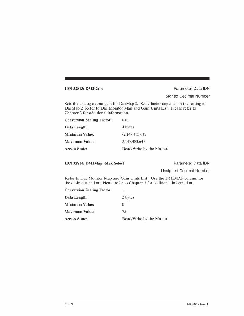
IDN 32813: DM2Gain Parameter Data IDN
Signed Decimal Number
Sets the analog output gain for DacMap 2. Scale factor depends on the setting ofDacMap 2. Refer to Dac Monitor Map and Gain Units List. Please refer toChapter 3 for additional information.
Conversion Scaling Factor: 0.01
Data Length: 4 bytes
Minimum Value: -2,147,483,647
Maximum Value: 2,147,483,647
Access State: Read/Write by the Master.
IDN 32814: DM1Map -Mux Select Parameter Data IDN
Unsigned Decimal Number
Refer to Dac Monitor Map and Gain Units List. Use the DMxMAP column forthe desired function. Please refer to Chapter 3 for additional information.
Conversion Scaling Factor: 1
Data Length: 2 bytes
Minimum Value: 0
Maximum Value: 75
Access State: Read/Write by the Master.
5 - 62 MA840 - Rev 1

IDN 32815: DM2Map -Mux Select Parameter Data IDN
Unsigned Decimal Number
Refer to Dac Monitor Map and Gain Units List. Use the DMxMAP column forthe desired function. Please refer to Chapter 3 for additional information.
Conversion Scaling Factor: 1
Data Length: 2 bytes
Minimum Value: 0
Maximum Value: 75
Access State: Read/Write by the Master.
IDN 32816: EncOut Parameter Data IDN
Unsigned Decimal Number
Sets the line count of the emulated encoder. Writing 0 to this IDN internallyconnects the EncIn input pins to the EncOut output buffers.
125, 250, 500, 1000, 2000, 4000, 8000, 16000 lines/rev
128, 256, 512, 1024, 2048, 4096, 8192, 16384 lines/rev
Note: The number of encoder counts per revolution is equal to 4 * encoder line count.
Conversion Scaling Factor: 1
Data Length: 4 bytes
Units: Emulated encoder count
Minimum Value: 0
Maximum Value: 16384
Access State: Read/Write by the Master.
MA840 - Rev 1 5 - 63

IDN 32817: InpMap1 Parameter Data IDN
Binary Data
Refer to Input Map List, Function Number Column for the desired function.
Set High/Low Polarity bits as required. Please refer to Chapter 3 for additionalinformation.
Conversion Scaling Factor: 1
Data Length: 2 bytes
Minimum Value: 0
Maximum Value: 0xFFFF
Access State: Read/Write by the Master.
IDN 32818: InpMap2 Parameter Data IDN
Binary Data
Refer to Input Map List, Function Number Column for the desired function.
Set High/Low Polarity bits as required. Please refer to Chapter 3 for additionalinformation.
Conversion Scaling Factor: 1
Data Length: 2 bytes
Minimum Value: 0
Maximum Value: 0xFFFF
Access State: Read/Write by the Master.
5 - 64 MA840 - Rev 1

IDN 32819: InpMap3 Parameter Data IDN
Binary Data
Refer to Input Map List, Function Number Column for the desired function.
Set High/Low Polarity bits as required. Please refer to Chapter 3 for additionalinformation.
Conversion Scaling Factor: 1
Data Length: 2 bytes
Minimum Value: 0
Maximum Value: 0xFFFF
Access State: Read/Write by the Master.
IDN 32820: InpMap4 Parameter Data IDN
Binary Data
Refer to Input Map List, Function Number Column for the desired function.
Set High/Low Polarity bits as required. Please refer to Chapter 3 for additionalinformation.
Conversion Scaling Factor: 1
Data Length: 2 bytes
Minimum Value: 0
Maximum Value: 0xFFFF
Access State: Read/Write by the Master.
MA840 - Rev 1 5 - 65

IDN 32821: InpMap5 Parameter Data IDN
Binary Data
Refer to Input Map List, Function Number Column for the desired function.
Set High/Low Polarity bits as required. Please refer to Chapter 3 for additionalinformation.
Conversion Scaling Factor: 1
Data Length: 2 bytes
Minimum Value: 0
Maximum Value: 0xFFFF
Access State: Read/Write by the Master.
IDN 32822: InpMap6 Parameter Data IDN
Binary Data
Refer to Input Map List, Function Number Column for the desired function.
Set High/Low Polarity bits as required. Please refer to Chapter 3 for additionalinformation.
Conversion Scaling Factor: 1
Data Length: 2 bytes
Minimum Value: 0
Maximum Value: 0xFFFF
Access State: Read/Write by the Master.
5 - 66 MA840 - Rev 1

IDN 32823: EncInFilt Parameter Data IDN
Unsigned Decimal Number
Sets the break frequency of the input filters on the Encoder Input pins.
Conversion Scaling Factor: 1
Data Length: 4 bytes
Units: Hz
Minimum Value: 50,000
Maximum Value: 16,000,000
Access State: Read/Write by Master.
EncMode Scaling Encoder Input Filter Setting
High Medium Low Lowest
(0) Quadrature Max QuadratureFreq.
1600000 800000 400000 200000
(1) StepDir Max Step Freq 800000 200000 100000 50000
(2) Up/Down Max Step Freq 800000 200000 100000 50000
(3) Hold Count N/A N/A N/A N/A N/A
MA840 - Rev 1 5 - 67

IDN 32824: RemoteFB Parameter Data IDN
Unsigned Decimal Number
Determines the source of Velocity and Position Feedback.
Conversion Scaling Factor: 1
Data Length: 4 bytes
Minimum Value: 0
Maximum Value: 2
Access State: Read/Write by Master in Phase 2.
RemoteFB Velocity Feedback Position Feedback
0 Resolver Resolver
1 Resolver Encoder
2 Encoder Encoder
IDN 32826: CommOff Parameter Data IDN
Signed Decimal Number
Allows the commutation offset to be set. For Pacific Scientific motors this shouldbe zero. For custom motors, this should be set for proper commutation.
Note: Negative numbers will be returned as the positive equivalent angle (modulo 360).
Conversion Scaling Factor: 0.001
Data Length: 4 bytes
Units: Electrical degrees
Minimum Value: -360,000
Maximum Value: 360,000
Access State: Read/Write by Master.
5 - 68 MA840 - Rev 1

IDN 32828: EncIn Parameter Data IDN
Unsigned Decimal Number
Allows the line count of input encoder to be defined. Must be set whenRemoteFB (IDN 32824) = 1 or 2.
Conversion Scaling Factor: 1
Data Length: 4 bytes
Units: Encoder line count
Minimum Value: 1
Maximum Value: 65535
Access State: Read/Write in phase 2Read Only in phases 3 and 4.
IDN 32829: ITThresh Parameter Data IDN
Unsigned Decimal Number
Allows the fault threshold for the IT Fault to be adjusted.
Conversion Scaling Factor: 1
Data Length: 4 bytes
Units: percent
Minimum Value: 0
Maximum Value: 100
Access State: Read/Write by Master.
Pacific Scientific Model Family Minimum Value Maximum Value
84X 0 60
MA840 - Rev 1 5 - 69

IDN 32830: StopTime Parameter Data IDN
Unsigned Decimal Number
The StopTime variable is associated with the RunStop I/O Function. It determinesthe maximum time after RunStop transitions to Stop that it will take the drive todisable. This IDN corresponds to an obsolete function. Do not use.
Conversion Scaling Factor: 0.001
Data Length: 2 bytes
Units: seconds
Minimum Value: 2
Maximum Value: 32,000
Access State: Read/Write by Master.
IDN 32831: VBusThresh Parameter Data IDN
Signed Decimal Number
Allows the Bus Undervoltage threshold to be set. If set to a negative number, turnsoff the bus undervoltage fault.
Conversion Scaling Factor: 1
Data Length: 2 bytes
Units: Volts
Minimum Value: -1
Maximum Value: 1,000
Access State: Read/Write by Master.
5 - 70 MA840 - Rev 1

IDN 32832: VelLmtHi Parameter Data IDN
Signed Decimal Number
Minimum value allowed for the velocity command into the velocity block. Alsosets the overspeed fault threshold if VelLmtHi VelLmtLo⟩ .
Overspeed fault set at ( )( )15. * max ,of VelLmtHi VelLmtLo
Conversion Scaling Factor: 0.001
Data Length: 4 bytes
Units: RPM
Minimum Value: -21,039,000
Maximum Value: 21,039,000
Access State: Read/Write by Master.
IDN 32833: VelLmtLo Parameter Data IDN
Signed Decimal Number
Minimum value allowed for the velocity command into the velocity block. Alsosets the overspeed fault threshold if VelLmtHi VelLmtLo⟩ .
Overspeed fault set at ( )( )15. * max ,of VelLmtHi VelLmtLo .
Conversion Scaling Factor: 0.001
Data Length: 4 bytes
Units: RPM
Minimum Value: -21,039,000
Maximum Value: 21,039,000
Access State: Read/Write by Master.
MA840 - Rev 1 5 - 71

IDN 32835: CoastTime Parameter Data IDN
Unsigned Decimal Number
Allows the amount of time the drive will coast for after the bus voltage drops belowVBusThresh before generating undervoltage fault.
Conversion Scaling Factor: 1
Data Length: 2 bytes
Units: seconds
Minimum Value: 0
Maximum Value: 32
Access State: Read/Write by Master.
IDN 32836: CommEnbl Parameter Data IDN
Unsigned Decimal Number
Enables commutation of the motor current based on rotor position. When thedrive powers up CommEnbl is set to 1. When CommEnbl is set to 0, thecommutation angle of the current flowing in the motor windings is determined bythe value of CommOff. When CommEnbl is set to 1, the commutation angle isdetermined by the sum of CommSrc feedback device electrical angle and theCommOff variable.
Conversion Scaling Factor: 1
Data Length: 4 bytes
Minimum Value: 0
Maximum Value: 1
Access State: Read/Write by Master.
5 - 72 MA840 - Rev 1

IDN 32837: Motor 1 Name Parameter Data IDN
Binary Data
The Motor variable is a 32-bit long unsigned long integer which is used to identifythe waveshape downloaded to the PC840 controller. By convention the 4 ASCIIcharacter abbreviation of the motor name is converted to an integer anddownloaded along with the waveshape. For example, if this variable is 0x53494E45= ‘S’ (0x53) : ‘I’ (0x49) : ‘N’ (0x4E) : ‘E’ (0x45).
Used to assign a label to Wave Shape Generation Table created
Conversion Scaling Factor: 1
Data Length: 4 bytes
Minimum Value: 0
Maximum Value: 0xFFFFFFFF
Access State: Read/Write in Phase 2.Read Only in Phase 3 and 4.
IDN 32838: Motor 2 Name Parameter Data IDN
Binary Data
The Motor variable is a 32-bit long unsigned long integer which is used to identifythe waveshape downloaded to the PC840 controller. By convention the 4 ASCIIcharacter abbreviation of the motor name is converted to an integer anddownloaded along with the waveshape.
Used to assign a label to Wave Shape Generation Table created
Conversion Scaling Factor: 1
Data Length: 4 bytes
Minimum Value: 0
Maximum Value: 0xFFFFFFFF
Access State: Read/Write in Phase 2.Read Only in Phase 3 and 4.
MA840 - Rev 1 5 - 73

IDN 32840: Kvff Parameter Data IDN
Unsigned Decimal Number
Allows following error to be reduced when running at a constant speed. When thedrive is commanded to run at a constant speed, kvff = 1000 will reduce the steadystate following error to zero, but will cause overshoot. A value of 700 is typicallyused.
Conversion Scaling Factor: 0.1
Data Length: 2 bytes
Units: percent
Minimum Value: 0
Maximum Value: 1,999
Access State: Read/Write by the Master.
IDN 32841: ARZ0 Parameter Data IDN
Unsigned Decimal Number
ARZ0 is the first velocity loop compensation zero. Please refer to Chapter 4 foradditional information.
Conversion Scaling Factor: 1
Data Length: 4 bytes
Units: Hz
Minimum Value: 20
Maximum Value: 100,000
Access State: Read/Write by the Master.
5 - 74 MA840 - Rev 1

IDN 32842: ARZ1 Parameter Data IDN
Unsigned Decimal Number
ARZ0 is the second velocity loop compensation zero. Please refer to Chapter 4for additional information.
Conversion Scaling Factor: 1
Data Length: 4 bytes
Units: Hz
Minimum Value: 20
Maximum Value: 1,000,000
Access State: Read/Write by the Master.
IDN 32843: ARF0 Parameter Data IDN
Signed Decimal Number
ARF0 is the first velocity loop compensation anti-resonance low-pass filter cornerfrequency. Please refer to Chapter 4 for additional information.
Conversion Scaling Factor: 0.01
Data Length: 4 bytes
Units: Hz
Minimum Value: -10,000,000
Maximum Value: 10,000,000
Access State: Read/Write by the Master.
MA840 - Rev 1 5 - 75

IDN 32844: ARF1 Parameter Data IDN
Signed Decimal Number
ARF1 is the second velocity loop compensation anti-resonance low-pass filtercorner frequency. Please refer to Chapter 4 for additional information.
Conversion Scaling Factor: 0.01
Data Length: 4 bytes
Units: Hz
Minimum Value: -10,000,000
Maximum Value: 10,000,000
Access State: Read/Write by the Master.
IDN 32845: Firmware Version Parameter Data IDN
Text
Allows the Master to read a TEXT description of the current versions fo the ARMand the DSP firmware: DSP Version 1.20, ARM version 6.0.
Note: DSP and ARM versions continue to change with each build.
Conversion Scaling Factor: 1
Data Length: Byte list
Access State: Read Only by the Master.
5 - 76 MA840 - Rev 1

IDN 32846: Encoder Data Scaling Method Parameter Data IDN
Binary Data
Sets the working parameters for the Encoder Position.
Conversion Scaling Factor: 1
Data Length: 2 bytes
Minimum Value: 0x0A
Maximum Value: 0x18A
Access State: Read/Write in phase 2.Read Only in Phases 3 and 4.
Bit Number Bit Setting(1 = Inverted, 0 = Non-Inverted)
Bits 0-2 010 : Rotational Scaling.
Bit 3 1 : Parameter Scaling
Bit 4 0 : Degrees
Bit 5 0 : Reserved
Bit 6 0 : At the Motor Shaft
Bit 7 0 : Absolute format1 : Modulo format (IDN 32847)
Bit 8 0 : Non-Inverted Encoder Data1 : Inverted Encoder Data
MA840 - Rev 1 5 - 77

IDN 32847: Encoder Modulo Value Parameter Data IDN
Unsigned Decimal Number
Allows the master to set the Encoder Modulo value (IDN 32846).
Conversion Scaling Factor: 1
Data Length: 4 bytes
Minimum Value: 10
Maximum Value: 2,147,483,647
Access State: Read/Write in phase 2.Read Only in Phases 3 and 4.
IDN 32853 : CommSrc Parameter Data IDN
Unsigned Decimal
Selects between resolver, incremental encoder, or hall encoder feedback for motorcommutation.
Note: CommSrc (IDN 32853) must be set BEFORE PoleCount (IDN 32807).
Conversion Scaling Factor: 1
Data Length: 4 Bytes
Minimum Value: 0
Maximum Value: 2
Access State: Read/Write in all phases.
CommSrc Feedback Device
0 Resolver
1 Encoder
2 Hall Encoder
5 - 78 MA840 - Rev 1

IDN 32857: Resolver Position Parameter Data IDN
Unsigned Decimal Number
ResPos returns the absolute resolver position within one revolution. The PC840has 65536 resolver counts per revolution. This IDN will, therefore, return a valuebetween 0 and 65535. This IDN is NOT affected by Position Modulo (IDN 103).
Conversion Scaling Factor: 1
Data Length: 2 bytes
Minimum Value: 0
Maximum Value: 65535
Access State: Read/Write by the Master in phases 2-4.
IDN 32858: Last Fault Parameter Data IDN
Signed Decimal Number
Returns the last fault occurred in the drive. The value of this IDN is NOT clearedby a fault reset command. A user can clear Last Fault by explicity writing 0 to thisIDN. See IDN 129 for description of faultcodes.
Conversion Scaling Factor: 1
Data Length: 2 bytes
Minimum Value: 0
Maximum Value: 22
Access State: Read Only by the Master in phases 2-4.
MA840 - Rev 1 5 - 79

IDN 32859: Last ExtFault Parameter Data IDN
Signed Decimal Number
Returns the last extended fault occurred in the drive. The value of this IDN isNOT cleared by a fault reset command. A user can clear Last ExtFault by explicitywriting 0 to this IDN. See IDN 129 for description of extended faultcodes.
Conversion Scaling Factor: 1
Data Length: 2 bytes
Minimum Value: 0
Maximum Value: 69
Access State: Read Only by the Master in phases 2-4.
IDN 32866: ADOffset Parameter Data IDN
Signed Decimal Number
Adjusts the steady-state value of the analog command input.
Conversion Scaling Factor: 10,00
Data Length: 4 bytes
Units: volts
Minimum Value: -150,000
Maximum Value: 150,000
Access State: Read/Write by Master.
5 - 80 MA840 - Rev 1

IDN 32870: I2tThresh Parameter Data IDN
Unsigned Decimal Number
Allows I2*t motor protection threshold value. If I2tFilt exceeds I2tThresh, thedrive will fault.
Conversion Scaling Factor: 1
Data Length: 2 bytes
Units: % of Ipeak2
Minimum Value: 0
Maximum Value: 100
Access State: Read/Write by Master.
IDN 32871: I2tF0 Parameter Data IDN
Unsigned Decimal Number
I2tF0 sets the low pass filter break frequency for the filter used to implement theI2*t motor drive thermal protection.
I2tF0 and I2tThresh set the thermal protection for the motor. See IDN 32872(I2tFilt). If I2tFilt exceeds I2tThresh, the drive will fault.
Conversion Scaling Factor: 0.001
Data Length: 2 bytes
Units: Hertz
Minimum Value: 1
Maximum Value: 1,000
Access State: Read/Write by Master.
MA840 - Rev 1 5 - 81

IDN 32872: I2tFilt Parameter Data IDN
Unsigned Decimal Number
I2tFilt is the filtered value of the square of the currents flowing in the motor:
I2tFilt = [(IU2 + IV2 + IW2)* 100/Ipeak2] low pass filtered by I2tF0 (IDN 32871).
When I2tFilt exceeds the threshold value specified by I2tThresh, the drive will fault.
Conversion Scaling Factor: 0.001
Data Length: 4 bytes
Units: % of Ipeak2
Minimum Value: 0
Maximum Value: 100,000
Access State: Read Only by Master.
IDN 32875: HallState Parameter Data IDN
Unsigned Decimal Number
HallState indicates the value of the hall sensors.HallState = (4*Hall 3) + (2*Hall 2) + (1*Hall 1)
Conversion Scaling Factor: 1
Data Length: 2 bytes
Minimum Value: 0
Maximum Value: 7
Access State: Read Only by Master.
5 - 82 MA840 - Rev 1

IDN 32876: Offset Angle for Hall Sensors Parameter Data IDN
Unsigned Decimal Number
HallOffset sets the offset angle for the hall sensors. Hall signals are to be wired asshown in the Pacific Scientific High Performance Servo Drives Catalog. By defaultit’s value is set to 0 degrees.
Conversion Scaling Factor: 1
Data Length: 2 bytes
Units: electrical degrees
Minimum Value: 0
Maximum Value: 360
Access State: Read/Write by Master.
IDN 32878: Digital Command Counts Parameter Data IDN
Signed Decimal Number
DigitalCmd indicates the position of the external command encoder (J2-17 throughJ2-20) or the accumulation of step inputs if step-and-direction input format is used.By default it’s value is set = 0.
Conversion Scaling Factor: 1
Data Length: 2 bytes
Units: Encoder counts
Minimum Value: -65536
Maximum Value: 65535
Access State: Read by Master in all phases.
MA840 - Rev 1 5 - 83

IDN 32879: Digital Command Frequency Parameter Data IDN
Signed Decimal Number
DigitalCmdFreq indicates the frequency of the digital command signal. Is iscalculated from delta DigitalCmd at position loop update rate. Although the valuesreturned do not have fractional parts this variable is communicated as a floatingpoint quantity. By default it’s value is set = 0.
Conversion Scaling Factor: 0.01
Data Length: 4 bytes
Units: Hz
Minimum Value: -300,000,000
Maximum Value: 300,000,000
Access State: Read by Master in all phases.
IDN 32880: AnalogOut1 Parameter Data IDN
Signed Decimal Number
Allows the Master to set the voltage on Analog Output 1 when DacMap 1 equalszero. The scaling for this IDN is 5/128 Volts per least significant bit (lsb).
Conversion Scaling Factor: 0.001
Data Length: 2 bytes
Units: Volts
Minimum Value: -5,000
Maximum Value: 4,961
Access State: Read/Write by the Master.
5 - 84 MA840 - Rev 1

IDN 32881: AnalogOut2 Parameter Data IDN
Signed Decimal Number
Allows the Master to set the voltage on Analog Output 2 when DacMap 2 equalszero. The scaling for this IDN is 5/128 Volts per least significant bit (lsb).
Conversion Scaling Factor: 0.001
Data Length: 2 bytes
Units: Volts
Minimum Value: -5,000
Maximum Value: 4,961
Access State: Read/Write by the Master.
IDN 32882: Analog Current Limit Parameter Data IDN
Unsigned Decimal Number
Allows the Master the current limit set (float value) by the Analog Current Limitinput (J2-6)
Conversion Scaling Factor: 0.01
Data Length: 2 bytes
Units: % of Ipeak
Min: 0
Max: 10,000
Access State: Read only by the Master
MA840 - Rev 1 5 - 85

IDN 32883: Analog Current Limit Gain Parameter Data IDN
Unsigned Decimal Number
AnalogILmtGain allows the Master to set the scale factor (float value) for theAnalog Current Limit Input (J2-6).
Conversion Scaling Factor: 0.001
Data Length: 4 bytes
Units: % of Ipeak/Volt
Min: 0
Max: 5,000,000
Access State: Read/Write by the Master
IDN 32884: Analog Current Limit Filter Parameter Data IDN
Unsigned Decimal Number
AnalogILmtFilt allows the Master to set the low-pass filter break frequency (floatvalue) on the Analog Current Limit Input (J2-6).
Conversion Scaling Factor: 0.01
Data Length: 4 bytes
Units: Hertz
Min: 0
Max: 100,000,000
Access State: Read/Write by the Master
5 - 86 MA840 - Rev 1

IDN 32885: Current Limit Offset Voltage Parameter Data IDN
Signed Decimal Number
AnalogILmtOffset allows the Master to set the offset (in volts) that is added to theAnalog Current Limit Input (J2-6).
Conversion Scaling Factor: 0.001
Data Length: 2 bytes
Units: Volts
Min: -10,000
Max: +10,000
Access State: Read/Write by the Master
IDN 32886: Actual Positive Current Limit Parameter Data IDN
Unsigned Decimal Number
AnalogILmtPlus allows the Master to display the actual positive current limit floatvalue used by the drive.
Conversion Scaling Factor: 0.01
Data Length: 2 bytes
Units: % of peak current rating of drive
Min: 0
Max: 10,000
Access State: Read only by the Master
MA840 - Rev 1 5 - 87

IDN 32887: Actual Negative Current Limit Parameter Data IDN
Unsigned Decimal Number
AnalogILmtMinus allows the Master to display the actual negative current limit(float value) used by the drive.
Conversion Scaling Factor: 0.01
Data Length: 2 bytes
Units: % of peak current rating of drive
Min: 0
Max: 10,000
Access State: Read only by the Master
IDN 34817: Input Bit #1 Parameter Data IDN
Binary Data
Allows the Master to read the value of the Input Bit 1 located on J2-31Note: User must supply Input Power to have Input Circuitry to operate.
Conversion Scaling Factor: 1
Data Length: 2 bytes
Minimum Value: 0
Maximum Value: 1
Access State: Read Only by the Master.
5 - 88 MA840 - Rev 1

IDN 34818: Input Bit #2 Parameter Data IDN
Binary Data
Allows the Master to read the value of the Input Bit 2 located on J2-32.Note: User must supply Input Power to have Input Circuitry to operate.
Conversion Scaling Factor: 1
Data Length: 2 bytes
Minimum Value: 0
Maximum Value: 1
Access State: Read Only by the Master.
IDN 34819: Input Bit #3 Parameter Data IDN
Binary Data
Allows the Master to read the value of the Input Bit 3 located on J2-33 .Note: User must supply Input Power to have Input Circuitry to operate.
Conversion Scaling Factor: 1
Data Length: 2 bytes
Minimum Value: 0
Maximum Value: 1
Access State: Read Only by the Master.
IDN 34820: Input Bit #4 Parameter Data IDN
Binary Data
Allows the Master to read the value of the Input Bit 4 located on J2-34.Note: User must supply Input Power to have Input Circuitry to operate.
Conversion Scaling Factor: 1
Data Length: 2 bytes
Minimum Value: 0
Maximum Value: 1
Access State: Read Only by the Master.
MA840 - Rev 1 5 - 89

IDN 34821: Input Bit #5 Parameter Data IDN
Binary Data
Allows the Master to read the value of the Input Bit 5 located on J2-35.Note: User must supply Input Power to have Input Circuitry to operate.
Conversion Scaling Factor: 1
Data Length: 2 bytes
Minimum Value: 0
Maximum Value: 1
Access State: Read Only by the Master.
IDN 34822: Input Bit #6 Parameter Data IDN
Binary Data
Allows the Master to read the value of the Input Bit 6 located on J2-36.Note: User must supply Input Power to have Input Circuitry to operate.
Conversion Scaling Factor: 1
Data Length: 2 bytes
Minimum Value: 0
Maximum Value: 1
Access State: Read Only by the Master.
5 - 90 MA840 - Rev 1

IDN 34824: Input Port Parameter Data IDN
Binary Data
Allows the Master to read the entire Input Port. The data returned is in thefollowing format:
Bit Number Description Bit Number Description
Bit 0 Input Bit 1 Bit 4 Input Bit 5
Bit 1 Input Bit 2 Bit 5 Input Bit 6
Bit 2 Input Bit 3 Bits 8-15 undefined
Bit 3 Input Bit 4
Conversion Scaling Factor: 1
Data Length: 2 bytes
Minimum Value: 0
Maximum Value: 0x003F
Access State: Read Only by the Master.
IDN 34825: AnalogIn Parameter Data IDN
Signed Decimal Number
Allows the master to read the Analog Input on the base unit. Refer to the scalingfactor document for the correct Analog Input Scaling.
Conversion Scaling Factor: 0.001
Data Length: 4 bytes
Units: Volts
Minimum Value: -13,500
Maximum Value: 13,500
Access State: Read Only by the Master.
MA840 - Rev 1 5 - 91

IDN 34826: EncPos Parameter Data IDN
Signed Decimal Number
Accumulated Encoder Position.
Conversion Scaling Factor: 1
Data Length: 4 bytes
Units: Encoder counts
Minimum Value: -2,147,483,647
Maximum Value: 2,147,483,647
Access State: Read Only by the Master.
IDN 34833: Output Bit #1 Parameter Data IDN
Binary Data
Allows the Master to write the value to Output Bit 1 located on J2-42.Note: User must supply Output Power to have Output Circuitry to operate.
Conversion Scaling Factor: 1
Data Length: 2 bytes
Minimum Value: 0
Maximum Value: 1
Access State: Read/Write by the Master.
5 - 92 MA840 - Rev 1

IDN 34834: Output Bit #2 Parameter Data IDN
Binary Data
Allows the Master to write the value to Output Bit 2 located on J2-43.Note: User must supply Output Power to have Output Circuitry to operate.
Conversion Scaling Factor: 1
Data Length: 2 bytes
Minimum Value: 0
Maximum Value: 1
Access State: Read/Write by the Master.
IDN 34835: Output Bit #3 Parameter Data IDN
Binary Data
Allows the Master to write the value to Output Bit 3 located on J2-44.Note: User must supply Output Power to have Output Circuitry to operate.
Conversion Scaling Factor: 1
Data Length: 2 bytes
Minimum Value: 0
Maximum Value: 1
Access State: Read/Write by the Master.
IDN 34836: Output Bit #4 Parameter Data IDN
Binary Data
Allows the Master to write the value to Output Bit 4 located on J2-25.Note: User may use Out4 for relay signal. See Section 2 for additonal information.
Conversion Scaling Factor: 1
Data Length: 2 bytes
Minimum Value: 0
Maximum Value: 1
Access State: Read/Write by the Master.
MA840 - Rev 1 5 - 93

IDN 34840: PC840 Output Byte Parameter Data IDN
Binary Data
Allows the Master to read/write the entire Output Port. The data is in the followingformat:
Bit Number Description
Bit 0 Output Bit 1
Bit 1 Output Bit 2
Bit 2 Output Bit 3
Bit 3 Output Bit 4
Bits 4 - 15 undefined
Conversion Scaling Factor: 1
Data Length: 2 bytes
Minimum Value: 0
Maximum Value: 0x000F
Access State: Read/Write by the Master.
5 - 94 MA840 - Rev 1

6 Diagnostics and ProtectionCircuits
Introduction The drive is fully protected against “normal” abuse and has aseven segment LED on the front panel to indicate SERCOSring or drive status. The servo drive has the following specificprotections:
• Output motor short circuit protection line-to-line andline-to-neutral.
• Interface to Pacific Scientific's standard motor PTC or anormally closed thermostat to sense motor overtemperature.
• Internal monitoring of the power stage heat sinktemperature for drive over temperature.
• Bus over voltage detection.
• Bus under voltage fault with adjustable threshold.
• Incorporating the measured heat sink temperature thereis an excessive current I*t fault. This fault limits the peakcurrent time and intelligently changes the continuouscurrent fault trip dependent on the measured heat sinktemperature to limit the continuous output current.
• Control voltage under voltage detection.
• The user +5V output is short circuit to I/O RTNprotected.
• The user +24V output is short circuit protected.
• All control outputs are short circuit to I/O RTNprotected.
• When a drive is powered up without valid parameters thepower stage cannot be enabled and no damage occurs tothe drive.
MA840 - Rev 1 6 - 1

Fault generation The following sequence will occur when the protection circuitsgenerate a fault. The fault source is latched, the output stageis disabled, the Fault mappable output function is activated,and the LED indicates the appropriate fault code. Faults arecleared by activating the Fault Reset input or by turning theAC power OFF and then ON again.
FaultCode List The following table lists the PC840 fault codes.
FaultCode Fault Description
1 Velocity feedback (VelFB) over speed*
2 Motor over temperature
3 User +5V low
4 Continuous current fault
5 Drive over current (instantaneous)
6 Control ±12 V under voltage
7 Not Assigned
9 Bus over voltage detected by DSP, External Regen Fault
10 Not Assigned
11 Bus under voltage* (Only if VBus < VBusThresh)
12 Ambient temperature too low
13 Encoder alignment failed*
14 Software and non-volatile memory versions not compatible
15 Hardware not compatible with software version
16 UnConfigured drive fault
17 Two AInNull events too close together
18 Position following error fault
19 Parameter memory error*
20 Initialization fault*
21 Drive over temperature
22 Resolver Fault
*To further identify this fault see software variable ExtFault.
6 - 2 MA840 - Rev 1

ExtFault The following table lists the values for ExtFault.
ExtFault ExtFault Description
1 Absolute Resolver Overspeed. |VelFB| > 21038 RPM
2 Variable Resolver Overspeed. |VelFB| > max(VelLmtxx)*1.5
3 Calibration data corrupted*
4 Excessive dc offset in current feedback sensor*
5 DSP incompletely reset by line power dip*
8 Excessive dc offset in Analog Command A/D*
9 Not Assigned
10 DSP stack overflow*
12 Software and control card ASIC incompatible*
13 Actual Model not same as stored in NV memory*
14 Unable to determine power stage*
15 Drive non-volatile parameters corrupt*
16 RAM failure*
17 Calibration RAM failure*
18 Encoder alignment: no motion fault
19 Encoder alignment: excessive motion fault
20 Encoder alignment: motor not settled
21 Encoder alignment: test failed
22 Encoder alignment: motion overflow fault
23 Hall Commutation: invalid configuration
24 Hall Commutation: overspeed
25 Hall Commutation: invalid hall state
26 Hall Commutation: invalid hall transition
27 I*t Drive
28 I^2*t Motor
MA840 - Rev 1 6 - 3

ExtFault (cont’)d
ExtFault ExtFault Description
29 DP RAM Test A *
30 DP RAM Test 5 *
31 DP RAM Test Run 1*
32 DP RAM Test Run 0 *
33 DP RAM Test C *
65 Data Read Only
66 Data Bounds Error
67 Execute no such command
68 RT not Implemented
69 FC not Implemented
*These fault states CANNOT be reset with the Fault Resetfunction and require the line control power to be turned OFFand ON again.
6 - 4 MA840 - Rev 1

6.1 Troubleshooting
Introduction A table of faults and their possible causes is listed below.
FaultCode Possible Cause
1 Loose or open circuit wiring to the resolver feedback connector J3.
Actual motor speed exceeded 1.5 * (Max Of |VelLmtLo| or|VelLmtHi|) or 21,038 RPM which is the over speed trip level.
For Encoder velocity feedback (RemoteFB = 2) check that EncIn isset properly.
2 Loose or open circuit wiring to motor PTC thermal sensor (J3-8,J3-9).
High ambient temperature at motor.
Insufficient motor heat sinking from motor mounting.
Operating above the motor’s continuous current rating.
3 Short circuited wiring on the output (J2-25).
4 Mechanically jammed motor.
Motion profile accelerations too high.
Machine load on the motor increased by a friction.
Problem with wiring between drive and motor yielding impropermotion.
Drive and/or motor under sized for application.
Note: See HSTemp, ItFilt, and ItF0 for information on measuringthermal margin in an application.
MA840 - Rev 1 6 - 5

Fault Codes
FaultCode Possible Cause
5 Motor power wiring (TB1-4, 5, or 6) short circuitline-to-ground/neutral.
Motor power cable length is enough longer than the data sheetspecification to cause excessive motor line to earth ground/neutralcapacitance.
Internal motor winding short circuit.
Insufficient motor inductance causing output over current faults.
KIP or KII improperly set causing excessive output currentovershoots.
6 Insufficient control AC voltage on TB1-1 to TB1-2.
External short on signal connector.
Internal drive failure.
7 Not Assigned.
9 Disconnected external regeneration resistor on TB1.
External regeneration resistor ohmage too large yielding BusOverVoltage fault.
External regeneration resistor short circuit.
Motor AC power input voltage too high.
10 Not Assigned.
11 Check the measured bus voltage VBus and the fault thresholdVBusThresh to make sure they are consistent.
12 Ambient temperature is below drive specification.Drive’s internal temperature sensor has a wiring problem.
13 Encoder Alignment failure. See ExtFault for additional information.
14 Not Assigned.
6 - 6 MA840 - Rev 1

Fault Codes
FaultCode Possible Cause
15 Attempt to upgrade the drive’s software will not work.Contact factory for upgrade details.
Resolver wiring error. Remove J2 and J3 connectors.Turn AC power OFF and then ON again.If FaultCode = 2, then correct resolver excitation wiring.
Internal failure. Return to factory for repair.
16 Unconfigured drive (Red and Green LEDs blinking after power up)was fully configured with the drive motor power enable active. Thisfault can be reset or the control AC power turned OFF and thenON again to get the drive-motor operating.
17 The AInNull function was re-activated too soon after going inactive.This can be caused by switch bounce on the input pin mapped toactivate AInNull.
18 The motor is either stalled or partially jammed.
The value for PosErrorMax is set too sensitive for the loop tuningand commanded motion profiles.
19 Glitch while last saving the NV parameters.Corrupted NV memory contents.Hardware problem with the NV memory.Re-Download parameters to restore drive operation.
20 Initialization Failure. See ExtFault for additional information.
21 High drive ambient temperature.Restriction of cooling air due to insufficient space around unit.
Operating above the drive’s continuous current rating.
Note: See HSTemp, ItFilt, and ItF0 for information on measuringthermal margin in an application.
22 Resolver signal is lost or intermittent. Check resolver cable.
MA840 - Rev 1 6 - 7

6.2 Motor Commutation
IDN 32807 Number of motor magnetic poles (Polecount), which is thesame as twice the number of motor electrical cycles permechanical revolution. This IDN should be set so that:
For resolver based commutation (IDN 32853 = 0):
IDN 32807 (PoleCount) = Number of motor poles
For encoder based commutation (IDN 32853 = 1):
IDN 32807 (PoleCount) = Number of encoder counts /electrical cycle.
IDN 32807 = 4 * IDN 32828 / (Motor poles / 2)
Note: For encoder based commutation, it is required to do anencoder alignment using IDN 32854.
Example If the application uses resolver based commutation with anR-Series motor, set IDN 32807 = 4 (R-Series motors have 4poles).
If the application uses resolver based commutation with anS-Series motor, set IDN 32807 = 6 (S-Series motors have 6poles).
If the application uses encoder based commutation with anR-Series motor and an 1024 line count encoder, set IDN 32807= 4 * 1024 / (4/2) = 2048.
Note: CommSrc (IDN 32853) must be set before PoleCount(IDN 32807).
IDN 32826 CommOff sets the origin for the electrical commutation angle.This IDN should be set so that for Pacific Scientific motors:
IDN 32826 (CommmOff) = 0
6 - 8 MA840 - Rev 1

6.3 System protection
Current Limits To protect the motor and drive, set the ILmts to:
IDN 82 Clockwise Current Limit (IlmtPlus). This IDN should be setso that:
IlmtPlus = min(100%, 100% * 5 * ICS/IPeak)
where ICS is the motor’s rms terminal current rating
IDN 82 = % of Ipeak * 10(i.e. for a 9x3 IlmtPlus of 50% or 7.5A set IDN 82 to 500)
IDN 83 Counter-Clockwise Current Limit (IlmtMinus). This IDNshould be set so that:
IlmtMinus = min(100%, 100% * 5 * ICS/IPeak)
where ICS is the motor’s rms terminal current rating
IDN 83 = % of IPeak * 10(i.e. for a 9x3 IlmtMinus of 50% or 7.5A set IDN 83 to 500)
Note: Application requirements may constrain the ILmts evenfurther.
MA840 - Rev 1 6 - 9

IDN 32829 ItThresh sets the maximum continuous output current, as apercentage of Ipeak, before the I*T thermal protection faultsthe drive. This IDN should be set so that:
IDN 32829 (ItThresh) = min(60%, 100%*3*IMTRcontinuous/IPR)
IPeak The following tables list the peak current rating for each of thedrives in the PC800 family.
Pacific ScientificModel
Ipeak (Amps)
8X2 7.5
8X3 15.0
8X4 30.0
6 - 10 MA840 - Rev 1

Appendix A Specifications
A.1 Output Power Specifications
PC8x2 PC8x3 PC8x4
Peak Output Current (RMS)1
5 seconds, (0 to 40°C) Ambient 5.3ARMS 10.6ARMS 21.2ARMS
Continuous Output Current (RMS)2
Convection (0 to 40°C) Ambient 2.7ARMS 3.6ARMS 7.1ARMS
Forced Air (0 to 40°C) Ambient3 N/A 5.3ARMS 10.6ARMS
Peak Output Power
Idealized Electrical Max(rectangular torque vs. speed)
2.25kW 4.5kW 9.0kW
Drive & Motor System Output Power
240 VAC three phase4
(5 seconds)1.35 to 2.7 to 5.4 to1.58kW 3.15kW 6.3kW
240 VAC single phase(1 second)
1.25 kW 2.5 kW 5.0 kW
120 VAC single phase(1 second)
.63 kW 1.25 kW 2.5 kW
MA840 - Rev 1 A - 1
1 To convert ARMS to A (0-pk) multiply ARMS * 1.41.Peak current (5 sec): PC843 = 15A (0-pk), PC844 = 30A (0-pk)
2 Above 40°C ambient, linearly derate so that 50°C rating = 0.67*40°C rating.
3 Forced air requires 3.6” x 1” fan mounted 2” below the drive.
4 Varies with the motor. Maximum peak output power with most motors is between60% to 70% of Idealized Electrical Max.

A.1 Output Power Specifications (Cont’d)
PC8x2 PC8x3 PC8x4
Continuous Output PowerDrive & Motor System@ Convection Ambient
240 VAC three phase 1.1kW 1.5kW 3.0kW
240 VAC single phase 1.1kW 1.5kW 2.0kW*
120 VAC single phase 550W 750W 1.0kW*
RMS Line Current@ Continuous Output PowerConvection Ambient
240 VAC three phase 4.5 A 6 A 12 A
240 VAC single phase 9 A 12 A 16 A*
120 VAC single phase 9 A 12 A 16 A*
*Single phase operation of the PC8x4 requires derating of continuous output powerto avoid excessive line and front end currents.
Power Stage Efficiency@ Pcont
98% 98% 98%
Shunt Regulator Power
Peak Power (500 mSec) 12.8kW 12.8kW 12.8kW
Continuous Power** 800W 800W 800W
Maximum External RegenDuty Cycle
6% 6% 6%
Bus Capacitance Energy Absorption
From 320V Nominal Bus 20J 30J 40J
**See Appendix E, Using External Regen for additional information.
A - 2 MA840 - Rev 1

A.1 Output Power Specifications (Cont’d)
PC8x2 PC8x3 PC8x4
Output Current Ripple Freq fs 20 kHz 20 kHz 16 kHz
Minimum MotorInductance l-l
4.0mH 2.0mH 1.25mH
Maximum MotorInductance l-l
4H 2H 1H
Maximum Motor PowerCable Length
-------------50 m/164ft------------
A.2 Input Power Specifications
The drive is capable of direct line operation. All units are fully isolated and do notrequire external isolation transformers. Also, the inrush current on the connectionto the line is internally limited to a safe level for the drive. There are no voltageselection or ranging switches required to operate within the specified voltage inputranges. It is the responsibility of the user to supply appropriate fuses or circuitbreakers in the TB1 AC Power motor power lines to comply with local electricalcodes.
The control input power required should be between 15 and 25 Watt. The ACinput motor power depends on output power and the losses in the power stage.The control power input has a single UL/CSA rated fuse in line with one of theAC line inputs.
MA840 - Rev 1 A - 3

PC800 Control Power Supply
Input Voltage Range
85 to 265 VAC,47 - 440 Hz single phase or 130 to 370 Vdc
Ride Through TimeFor AC Line Drop
90 VAC 50 Hz >0.7 50 Hz cycle120 VAC 60 Hz >2.1 60 Hz cycles240 VAC 60 Hz >13.3 60 Hz cycles
PC830 Motor AC Power Supply
Model
Number
Voltage Range Phases Transformer
Suggested kVA
Maximum
AC Line* kVA
PC8x2 90-265 Vac 1 or 3 1.5 to 3 kVA 100 kVA
PC8x3 90-265 Vac 1 or 3 2 to 4 kVA 100 kVA
PC8x4 180-265 Vac 3 3 to 6 kVA 250 kVA
*Maximum AC Line is specified to limit the line surges coupled to the drive.
Bus Voltage (nominal, standard drive)
240 VAC Three Phase Input . . . . 320 VDC
120 VAC Single Phase Input . . . 155 VDC
PC840 InrushCurrent & Fusing
Model
Number
InrushPeak
Current
InrushPulse
Width
Fuse Type Manufacturer,
Part Number
PC8x2 300 A 0-p 1.0 msec 10 A 250 V TimeDelay
Bussmann, MDA-10
PC8x3 300 A 0-p 1.5 msec 20 A 250 V TimeDelay
Bussmann, MDA-20
PC8x4 300 A 0-p 2.0 msec 30 A 250 V Slo-Blo Littlefuse, FLM 30
A - 4 MA840 - Rev 1

A.3 Performance Characteristics
Note: Unless otherwise specified, the below specifications are worst case limits andapply over the specified operating ambient temperature and over the specified operatingline voltage.
Motor Current Control
Motor Phase Current Waveform Back EMF Matched Pseudo Sine
Motor Shaft Torque(Ignoring motor magnetic saturation)
Peak (hot)5 Kt (Nm/ARMS)*Drive Ipeak(ARMS)
Instantaneous Kt (Nm/ARMS)*IFB 2
Bandwidth
Maximum Bandwidth 1.5 kHz
Recommended Bandwidth 1.0 kHz
Bandwidth Variation For Fixed Motor L ± 10%
Bandwidth Variation For ± 25%
AC Line Variation ± 2%
Update Period 62.5 µsec
Recommended Motor Electrical Frequency < 400 Hz
MA840 - Rev 1 A - 5
5 Multiply by 1.06 for cold KT (PMA motors).

Analog Command
Maximum Differential Range ±13.5 Volts
Maximum Single Ended Range ±21 Volts
Full Scale Tolerance ±5% (worst case)
±1% (typical)
Linearity 0.1% Full Scale
Monotonic to < 2-16 Full Scale
S/N Ratio Referred to Full Scale
Full A/D Bandwidth 14 bits
150 Hz A/D Bandwidth 16 bits
10 Hz A/D Bandwidth 18 bits
Offset Adjustable to 0
Maximum Unadjusted Offset 50 mV
Offset Drift 250 µV/°C typ.
CMRR > 30 dB @ 60 Hz
Digital Position Commands
Modes Quadrature Encoder, Step &Direction, or Up & Dn Count
Maximum Input Rate For Fast Decode
Quadrature Decode Max Line Frequency 800 kHz
Step/Dir Decode Max Step Frequency 800 kHz
Up/Dn Count Max Frequency 800 kHz
Minimum Fast Decode Pulse Width 0.6 µSec
Fast Decode Direction Setup Time 0.6 µSec
Fast Decode Direction Hold Time 0.6 µSec
Relative Timing For Filtered Decode 4, 8, or 16 to 1e.g. Max Step Freq 800, 200, 100,or 50 kHz
A - 6 MA840 - Rev 1

Velocity Loop
Maximum Stable Bandwidth > 400 Hz
Update Period 250 µSec
Range 0 to 21,000 RPM
Command Resolution < 0.001 RPM
Velocity Loop Compensation Parameters
KVP Range (Depends on Ipeak) 0 to 12.6 (Ipeak)(1/rad/sec)
KVP Resolution 16 bit
KVI Range 0 to > 200 Hz
KVI Resolution 16 bit
ARF0* Range 0.01 to > 1e5 Hz
ARF1* Range 0.01 to > 1e5 Hz
ARZ0* Range 0 to > 1e5 Hz or off
ARZ1* Range 20 to > 1e5 Hz or off
CMDGAIN Range 0 to ±15,000 RPM/V
0 to ±10(Ipeak) V-1
CMDGAIN Resolution ≥ 16 bit mantissa
*ARx0 set to a negative number allows complex poles/zeros. In this case, ARx1becomes the Q and the corresponding |ARx0| is the frequency in Hz.
MA840 - Rev 1 A - 7

Position Loop
Maximum Stable Bandwidth > 100 Hz
Update Period 1 mSec
Position Range 0 to ± 32768 Rev
Position Error Range 0 to ± 4500 Rev
Command Resolution 2-16 Rev = 0.33 arc min
Position Loop Compensation Parameters
KPP Range 0 Hz to > 150 Hz
KPP Resolution 16 bit
KVFF Range 0 to 199.9%
KVFF Resolution 16 bit
General
Max Delay AC Line To Control Supply On 1.0 Sec
Max Delay AC Line To Fully Operational 2.0 Sec
Environmental
Storage Temperature -40°C to 70°C
Humidity, non-condensing 10% to 90%
Altitude 1500 m (5000 feet)
A - 8 MA840 - Rev 1

A.4 Resolver Feedback Specifications
Note: Unless otherwise specified, the below specifications are worst case limits andapply over the specified operating ambient temperature and over the specified operatingline voltage.
Resolver Position Signal
Resolution/Rev 24 bits = 0.0013 arc min
Repeatability < ±2-18 Rev = ±0.08 arc min rms
Noise
No Filtering < 2-16 Rev rms = 0.3 arc min rms
150 Hz Single Pole Filtered < 2-17 Rev rms = 0.16 arc minrms
10 Hz Single Pole Filtered < 2-19 Rev rms = 0.04 arc minrms
dc Offset Temperature Drift < 2-18 Rev/°C = 0.08 arc min/°C
Absolute Accuracy
Drive only ±2-12 Rev = ±5.3 arc min
Drive with 20 arc min resolver ±2-9.75 Rev = ±25 arc min
Software Update Time 1 mSec
MA840 - Rev 1 A - 9

Resolver Velocity Signal
Resolution < 0.001 RPM
Quanta = 0.0143 RPM
Noise
No Filtering < 3 RPM rms
150 Hz Single Pole Filtered < 0.6 RPM rms
10 Hz Single Pole Filtered < 0.06 RPM rms
DC Accuracy
Typical @ 25°C ±0.01%
Worst case ±0.05%
Ripple
Drive only 0.75% p-p at 1000 RPM
Drive with 20 arc min resolver 3% p-p at 1000 RPM
Offset < 0.0001 RPM
Software Update Time 250 µSec
Emulated Encoder Output Signals
Available Resolutions (PPR)
Binary 128, 256, 512, 1024, 2048, 4096,8192, 16384
Decimal 125, 250, 500, 1000, 2000, 4000,8000, 16000
Maximum Output Line Frequency 833 kHz
Max Recommended Speed @ 16384 PPR 2900 RPM
Max Recommended Speed @ 4096 PPR 11600 RPM
Marker Pulse Width ≈ 1 Quadrature Pulse
A - 10 MA840 - Rev 1

General
-3 dB Bandwidth > 1500 Hz
-45° Phase Lag > 400 Hz
Resolver Excitation Frequency 6510.42 Hz
Max Tracking Rate > 48600 RPM
Max Recommended Rate 25 kRPM
Max Tracking Acceleration > 16x106 RPM/Sec
Maximum Feedback Cable Length 50 m/164 ft
Nominal Frequency Response
MA840 - Rev 1 A - 11
1 10 100 1000 10000
FREQUENCY (Hz)
RESPOS
VelFB = RESPOS0.00025∆
MAGNITUDE
PHASE
+3 dB
0 dB
-6 dB
-24 dB
-12 dB
-18 dB
0 Deg
90 Deg
-90 Deg
-180 Deg
-270 Deg

The PC830 packaging is totally enclosed single axis panelmount. The figure on the next page gives the key dimensionsfor use in physically mounting the product. When mountingmultiple units on one panel there should be at least 20 mm(0.75") of air space on the sides and 40 mm (1.5") or air spaceabove and below the unit.
When mounting multiple drives in a row some customers havefound the stiffness of the drive and their mounting panel to betoo low. To increase the mounted mechanical integrity,connect to the threaded insert on the top front edge.
The overall drive panel dimensions and the mounted depth notincluding mating connectors is listed in the below chart. Theextra depth for mating connectors is 1.0" or less.
Dimensions
Model Height Width Depth
PC8x2 198.1 mm/7.8" 88.1 mm/3.47" 158 mm/6.22"
PC8x3 198.1 mm/7.8" 88.1 mm/3.47" 158 mm/6.22"
PC8x4 198.1 mm/7.8" 114 mm/4.49" 158 mm/6.22"
Weight
Model Weight
PC8x2 1.9 kg/4 lb
PC8x3 2 kg/4.3 lb
PC8x4 2.6 kg/5.7 lb
A - 12 MA840 - Rev 1

Drive Mechanical Outline
PC8X2/3/4
MA840 - Rev 1 A - 13
6.22[157,9]
7.80[198,1]
3.47[88,1]
4.52[114,8]
1.74[44,2]
7.280[184,91]
.26[6,6]
ø .290[7,37]
1.05[26,7]
6.64[168,7]

PC830 TerminalBlock Adapter
A - 14 MA840 - Rev 1
1.1529,2[ ]
2.25357,23[ ]
.338,3[ ]
1.8547[ ]
4.65118,1[ ]
.72518,42[ ]
.99425,24[ ]
3.23082,04[ ]
.0621,57[ ]
.67517,15[ ]
1.25031,75[ ]
.153,8[ ]
115
1
5 1
8122
2344 916
2 x 22 PIN CONNECTOR WECO P/N: 934-222 x 8 PIN CONNECTOR WECO P/N: 934-08

Fan Option Kit
MA840 - Rev 1 A - 15
.317,9[ ]
3.3885,7[ ]
4.00101,6[ ]
.389,5[ ]
2.0050,8[ ]
5.09129,4[ ]
2.2256,3[ ]
ø
MOUNTING FOR M4 OR #8-32TYP 2 PL.
.1724,37[ ]

Appendix B Model Identification
B.1 Servo Drive Package Order Numbering System
P C 8 X X - 0 0 1 - X
PC8 = Servo Drive Family Designation
4 = Command Interface Designation4 = SERCOS Network
3 = Power Level2 = 2.7 ARMS cont. @ 25 °C, 5.3 ARMS pk.3 = 3.6 ARMS cont. @ 25 °C, 10.6 ARMS pk.4 = 7.1 ARMS cont. @ 25 °C, 21.2 ARMS pk.
- 001 = Customization Code001 = Standard UnitXYZ = Factory Assigned Hardware Customization
X = AccessoriesN = No accessoriesA = Basic connector kitT = TB adapter connector kit
MA840 - Rev 1 B - 1

Example OrderNumbers
Order # Model # Description
PC843-001-T PC843-001-T 10.6 ARMS peak standard servo drive
CA800-TB TB adapter PC803 connector kit
MA840 PC840 User Manual
PC844-001-A PC844-001-A 21.2 ARMS peak standard servo drive
CA800 Basic PC804 connector kit
MA840 PC840 User Manual
PC844-001-N PC844-001-N 21.2 ARMS peak standard servo drive
MA840 PC840 User Manual
B.2 PC800 Accessories
Connector MateKits
CA800 15-pin and 44-pin d-subminiature mates for the PC80x servodrive.
CA800-TB 15-pin and 44-pin d-subminiature terminal block adapter matesfor the PC80x servo drive.
Manual andDocumentationKits
MA840 PC840 User Manual
Regen Resistors
PRK-200 External regen resisitor kit
Fan Kits
PFK-120 120 VAC Fan
PFK-240 240 VAC Fan
B - 2 MA840 - Rev 1