m2-3 buck converter objective is to answer the following questions: 1.how does a buck converter...
TRANSCRIPT

M2-3 Buck Converter
Objective is to answer the following questions:1. How does a buck converter operate?

Buck Converter
• The input voltage is always greater than the output voltage
12 V 5 VControl

Buck Configuration
• The input voltage is always greater than the output voltage
VOUT
VIN
VM
VGATE
LC
ISW
IL
VIN
time
20V
15V
10V
5V
0V
VOUT
time
7.5V
5V
2.5V
0V
10V
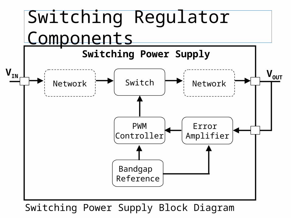
Switching Regulator Components
Switching Power Supply Block Diagram
VIN VOUT
Switching Power Supply
Switch
Error Amplifier
Bandgap Reference
PWMController
Network Network
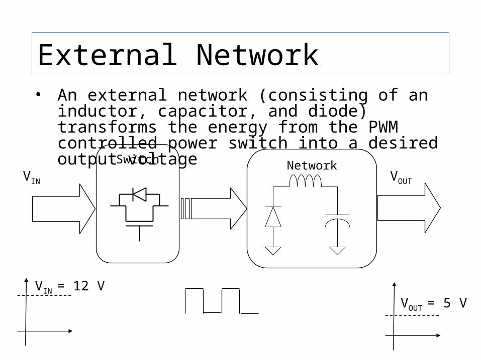
External Network• An external network (consisting of an inductor, capacitor,
and diode) transforms the energy from the PWM controlled power switch into a desired output voltage
NetworkSwitchVIN VOUT
VIN = 12 VVOUT = 5 V
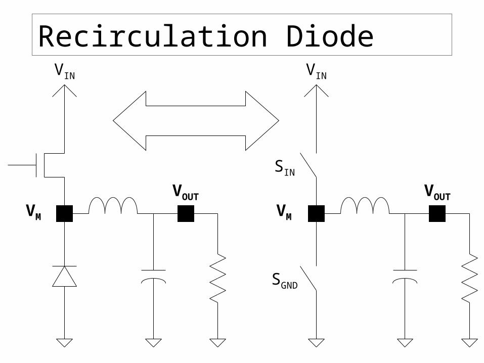
Recirculation Diode
VOUT
VIN
VOUT
VIN
SIN
SGND
VM VM
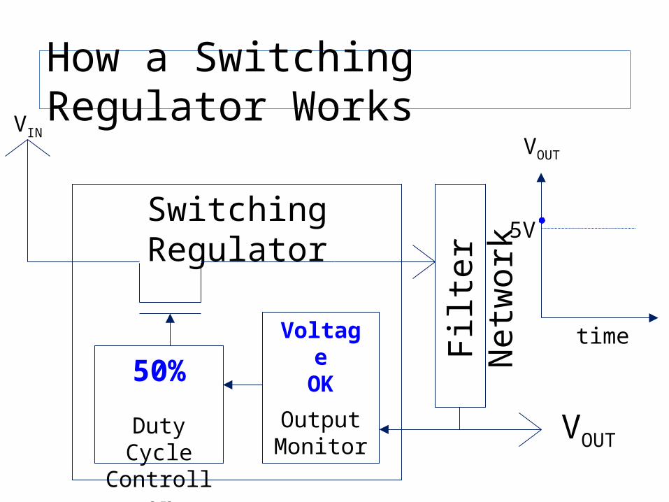
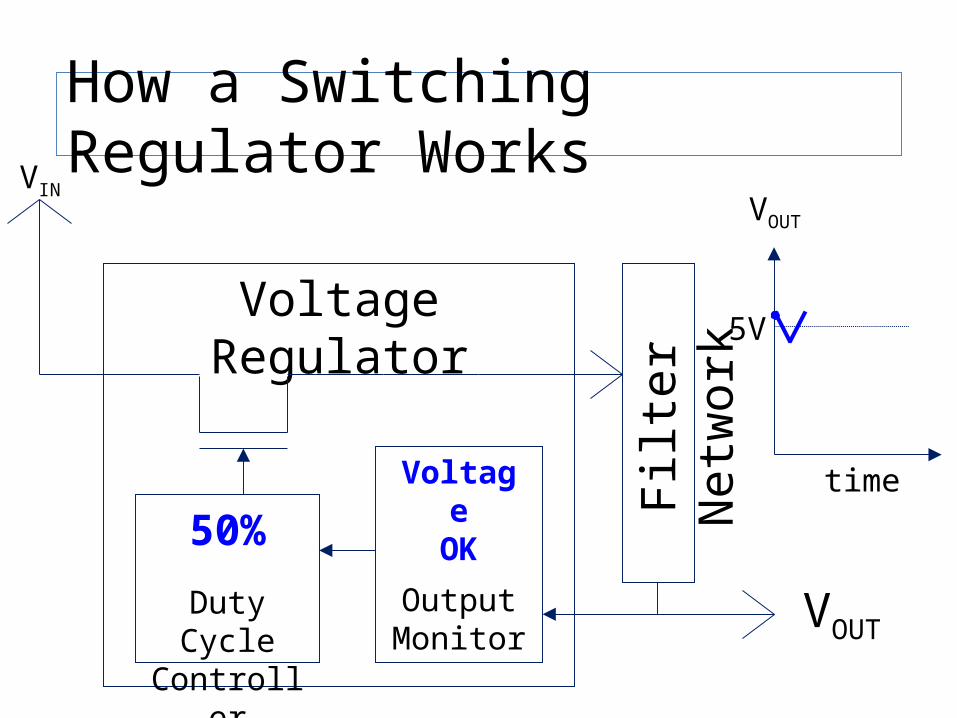
How a Switching Regulator WorksVIN
Switching Regulator
Duty Cycle Controller
OutputMonitor
VOUT
time
5V
VoltageOK50%
Filt
er N
etw
ork
VOUT

How a Switching Regulator WorksVIN
Voltage Regulator
Duty Cycle Controller
OutputMonitor
VOUT
time
5V
VoltageOK50%
Filt
er N
etw
ork
VOUT
How a Switching Regulator WorksVIN
Voltage Regulator
Duty Cycle Controller
OutputMonitor
VOUT
time
5V
VoltageOK50%
Filt
er N
etw
ork
VOUT
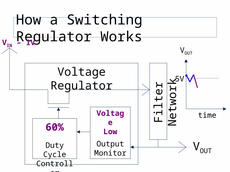
How a Switching Regulator WorksVIN – 1V
Voltage Regulator
Duty Cycle Controller
OutputMonitor
VOUT
time
5V
VoltageLow60%
Filt
er N
etw
ork
VOUT
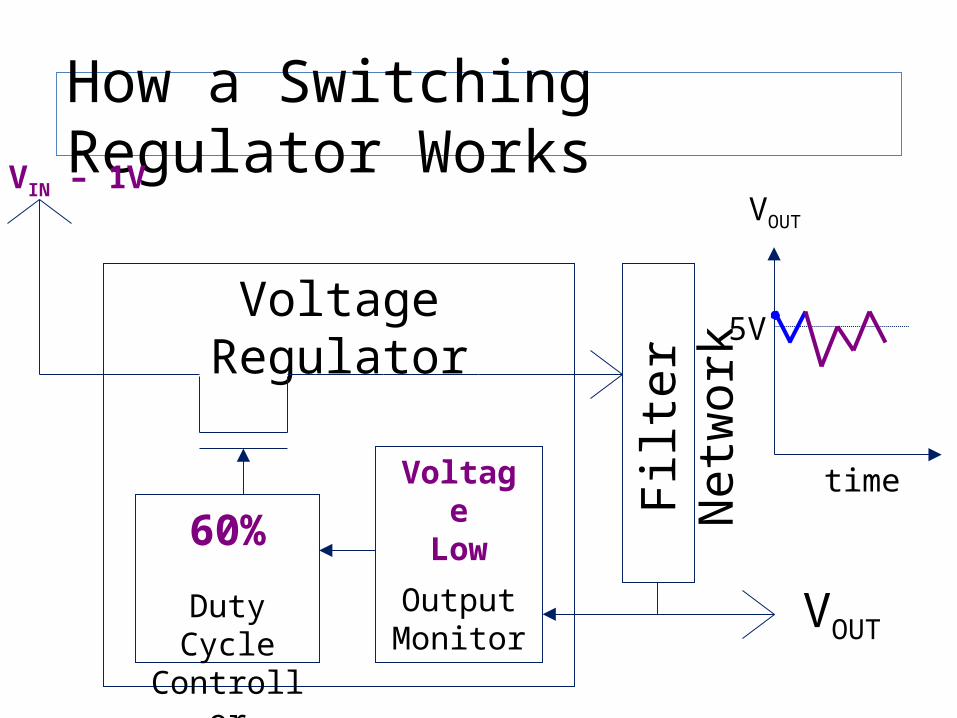
How a Switching Regulator WorksVIN – 1V
Voltage Regulator
Duty Cycle Controller
OutputMonitor
VOUT
time
5V
VoltageLow60%
Filt
er N
etw
ork
VOUT

How a Switching Regulator WorksVIN
Switching Regulator
Duty Cycle Controller
Output Monitor
VOUT
time
5V
VoltageOk50%
Filt
er N
etw
ork
VOUT
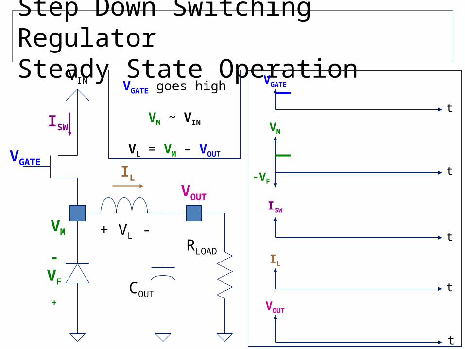
Step Down Switching RegulatorSteady State Operation
VOUT
VIN
VM
VGATE
+ VL -
COUT
ISW
IL
VGATE goes high
VM ~ VIN
VL = VM – VOUT
t
VM
t
VGATE
t
IL
VOUT
t
ISW
t
RLOAD
-VF
-VF
+

Step Down Switching RegulatorSteady State Operation
VOUT
VIN
VM
VGATE
COUT
ISW
IL
VL Constant
t
VM
t
VGATE
t
IL
VOUT
t
ISW
L LdI V= Constant
dt L
IL and ISW increase
t
RLOAD
COUT is charged by IL
and
VOUT increases
-VF
-VF
+
+ VL -

Step Down Switching RegulatorSteady State Operation
VOUT
VIN
VM
VGATE
COUT
ISW
IL
VGATE = 0V
The pass transistor
is turned off
ISW = 0At
VM
t
VGATE
t
IL
VOUT
t
ISW
t
RLOAD
LV
=dtdI LL
IL cannot go to 0A instantly:
VM goes negativeVL = VM – VOUT
L LdI V= < 0 A/s
dt L
-VF
-VF
+
+ VL -
Step Down Switching RegulatorSteady State Operation
VOUT
VIN
VGATE
COUT
ISW
IL
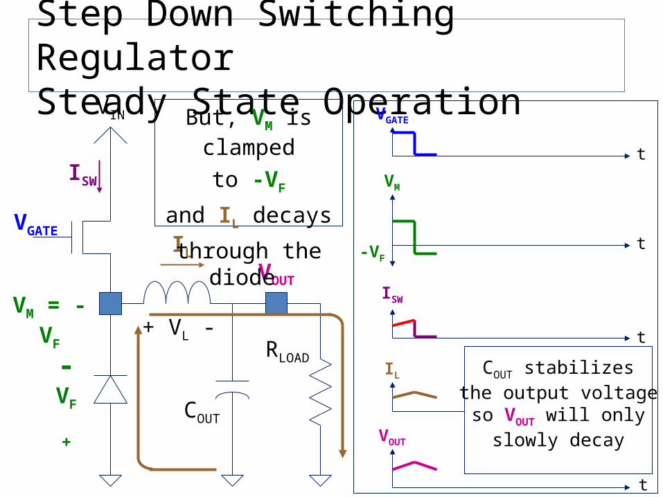
But, VM is clamped
to -VF
and IL decays
through the diode t
VM
t
VGATE
t
IL
VOUT
t
ISW
t
RLOADCOUT stabilizes
the output voltageso VOUT will only slowly
decay
-VF
VM = -VF
-VF
+
+ VL -
Step Down Switching RegulatorSteady State Operation
VOUT
VIN
VGATE
COUT
ISW
IL
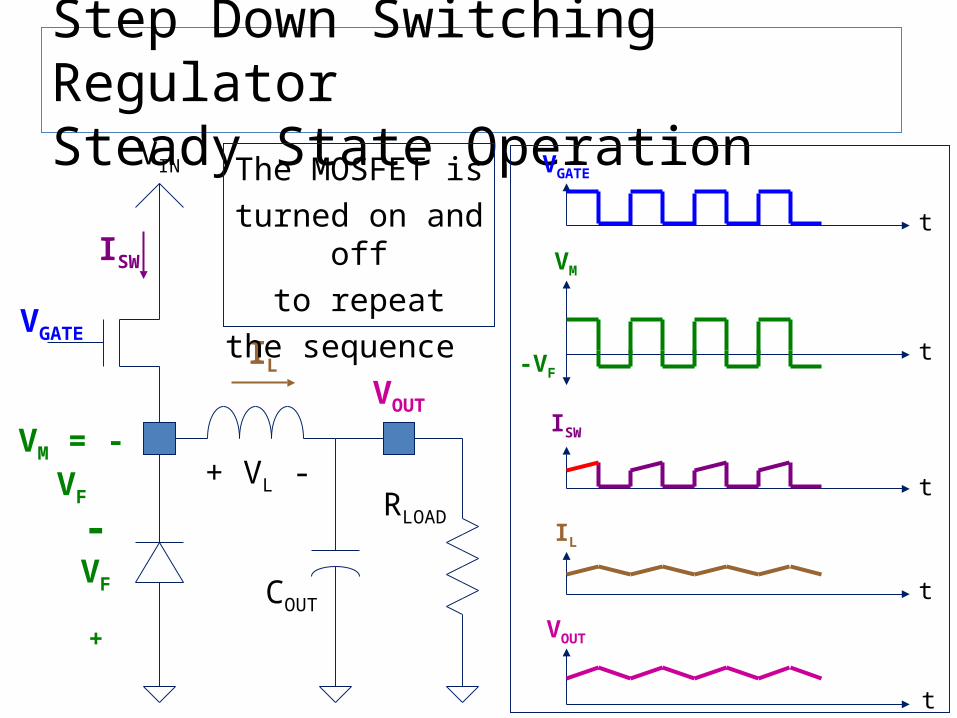
The MOSFET is
turned on and off
to repeat
the sequence
RLOAD
t
VM
t
VGATE
t
IL
VOUT
t
ISW
t
-VF
VM = -VF
-VF
+
+ VL -

Volt-Second Balance
VOUT
VIN
VM
VGATE
COUT
ISW
RLOAD IL
t
VGATE
t
+ VL -
IL
ConstantLV
dtdi LL

Volt-Second Balance
• In steady state, the inductor current ripples about an average, IL,AVG:
• Therefore, the total area (or volt-seconds) under the inductor voltage waveform is zero.
1-D TT DT
L L L0 0 DT
V (t)dt = V (t)dt + V (t)dt
VL
t
VIN - VOUT
-VOUT
TDT
(1-D)T
T
L IN OUT OUT0
V (t)dt = (V - V )DT +(-V )(1-D)T = 0
+ VL -+ VL -

Voltage-Second Principleand the DC Transfer Function
IN OUT OUT OUTV DT +(-V D+ V D- V )T = 0
OUT
IN
V=D
V
• From:
we can calculate the transfer function of the step down switching voltage regulator
T
L IN OUT OUT0
V (t)dt = (V - V )DT +(-V )(1-D)T = 0
IN OUTV DT +(-V )T = 0
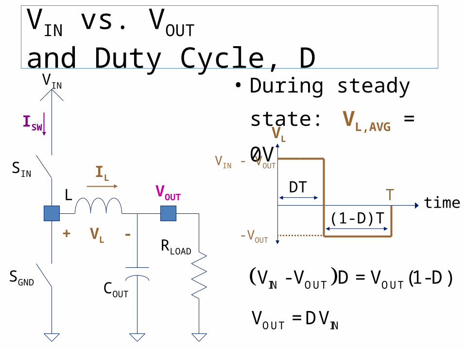
VIN vs. VOUT and Duty Cycle, D
VOUT
VIN
L
COUT
ISW
IL
RLOAD
SIN
SGND
• During steady state:
VL,AVG = 0V
+ VL -
VL
time
VIN - VOUT
-VOUT
TDT
(1-D)T
IN OUT OUTV - V D = V (1-D)
OUT INV = DV
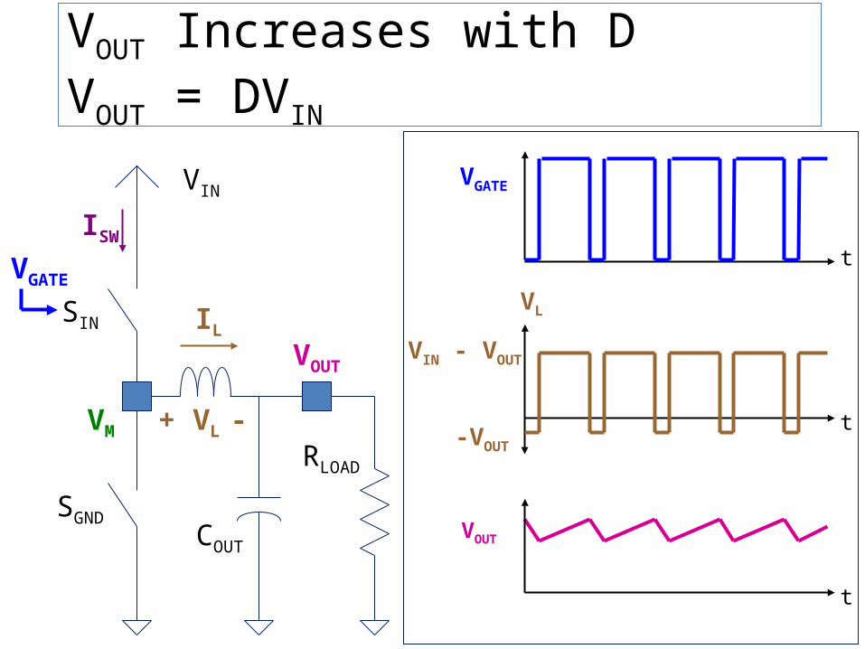
VOUT Increases with DVOUT = DVIN
VOUT
VIN
VM
VGATE
COUT
ISW
IL
VOUT
RLOAD
t
VL
t
VGATE
VIN - VOUT
t
+ VL - -VOUT
SIN
SGND
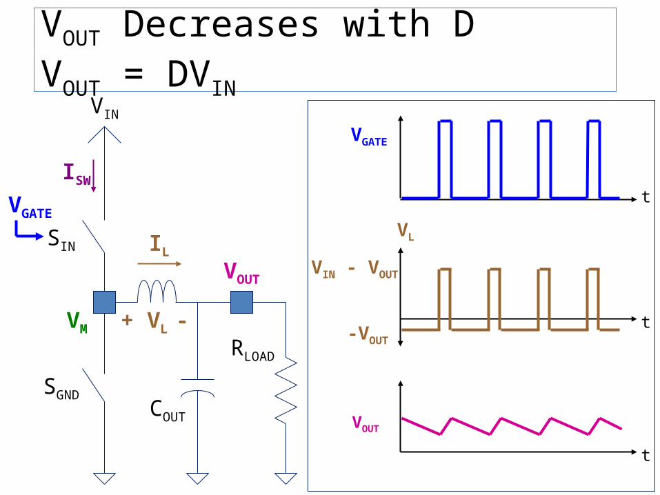
VOUT Decreases with DVOUT = DVIN
VOUT
t
VL
t
VGATE
VIN - VOUT
t
-VOUT
VOUT
VIN
VM
VGATE
COUT
IL
RLOAD
+ VL -
SIN
SGND
ISW

Ripple Current• Recall, IL is the sum of the
current flowing through SIN and SGND
VOUT
VIN
COUT
IL
RLOAD
SIN
SGND
IGND
time
ISW IGNDIL
IL,AVG
ISW

Memo

Memo