low-voltage digitally controlled current differencing buffered
TRANSCRIPT
This article appeared in a journal published by Elsevier. The attachedcopy is furnished to the author for internal non-commercial researchand education use, including for instruction at the authors institution
and sharing with colleagues.
Other uses, including reproduction and distribution, or selling orlicensing copies, or posting to personal, institutional or third party
websites are prohibited.
In most cases authors are permitted to post their version of thearticle (e.g. in Word or Tex form) to their personal website orinstitutional repository. Authors requiring further information
regarding Elsevier’s archiving and manuscript policies areencouraged to visit:
http://www.elsevier.com/copyright
Author's personal copy
Int. J. Electron. Commun. (AEÜ) 63 (2009) 249–258www.elsevier.de/aeue
Low-voltage digitally controlled current differencing buffered amplifier andits application
Worapong Tangsrirat∗, Danucha Prasertsom, Wanlop Surakampontorn
Faculty of Engineering and Research Center for Communications and Information Technology (ReCCIT), King Mongkut’s Institute ofTechnology Ladkrabang (KMITL), Chalongkrung Road, Ladkrabang, Bangkok 10520, Thailand
Received 13 March 2007; accepted 16 January 2008
Abstract
In this paper, a design of a low-voltage digitally controlled current differencing buffered amplifier (DC-CDBA) is intro-duced. The realization scheme is through the cascade connection of a current differencing circuit, a current division network(CDN) and a buffered voltage amplifier. To achieve the digital control of the current gain of the circuit, a novel CDN is alsoproposed. The proposed DC-CDBA can operate with the low supply voltage of ±1.25 V. PSPICE simulations using standard0.5-�m CMOS process parameters are in agreement with the theory. An application example using the proposed DC-CDBAsas active elements in the realization of the digitally tuned current-mode universal filter is also included.� 2008 Elsevier GmbH. All rights reserved.
Keywords: Current differencing buffered amplifier (CDBA); Current division network (CDN); MOS transistor; Current-mode circuit
1. Introduction
Programmable tuning characteristic of an analog circuitis an attractive feature that is widely used in several use-ful applications. In analog signal processing area, there aremany engineering applications which require programmablecharacteristics such as, adaptive filters, music synthesizers,formant speech synthesizers and tracking filters [1–4]. Gen-erally, analog or digital tuning can be employed to controlthe circuit parameters. However, in low-voltage applications,there is a limitation on the allowable range of the analog tun-ing voltage. Hence, in these applications, the digital controlis more attractive [5]. Another example utilizing digital con-trol is the interface with the digital signal processing (DSP)unit in the modern digital system. For example, in mod-ern wireless systems, all of the baseband signal processingare implemented digitally by DSP unit. There are baseband
∗ Corresponding author. Tel.: +66 2 739 0757; fax: +66 2 326 4225.E-mail address: [email protected] (W. Tangsrirat).
1434-8411/$ - see front matter � 2008 Elsevier GmbH. All rights reserved.doi:10.1016/j.aeue.2008.01.006
analog blocks required in the integrated wireless receiversuch as highly linear filter section for out-of band blockersattenuation, tunable filter section for channel selection, andvariable gain amplifier for providing programmable gain set-ting and a primary requirement of those baseband analogblocks are to be digitally controlled [5]. Therefore, digitallyprogrammable tuning characteristics have been an ongoingresearch topic for a number of years.
In 1999, a new active building block circuit, namely cur-rent differencing buffered amplifier (CDBA), was first in-troduced to provide new possibilities in the circuit synthesisand to simplify the circuit implementation [6,7]. The CDBAis suitable for integrated circuit (IC) implementation in bothbipolar and CMOS technologies [7–12]. Moreover, sincethe CDBA can be considered as a collection of current- andvoltage-mode unity gain cells, it has large dynamic range andquite wide bandwidth similar to its current-mode counter-parts such as, current feedback operational amplifiers (CFAs)and second generation current conveyors (CCIIs). Owingto these advantages of the CDBA, in this paper we present

Author's personal copy
250 W. Tangsrirat et al. / Int. J. Electron. Commun. (AEÜ) 63 (2009) 249–258
a digitally controlled CDBA (DC-CDBA) with low supplyvoltage operation. The proposed DC-CDBA is realized byinterconnecting a current differencing circuit, a current di-vision network (CDN), and a unity-gain voltage amplifier.The novel CDN circuit is also proposed in order to providethe digital control of the current gain of the DC-CDBA. Anapplication of the proposed DC-CDBA in realizing digitallyprogrammable current-mode universal filter with the advan-tage of linearly tuned frequency to the digitally controlledparameter has also been discussed. PSPICE simulation re-sults of the proposed low-voltage DC-CDBA and its appli-cation are included.
2. Circuit configurations
2.1. Basic concept
The proposed DC-CDBA is a versatile analog buildingblock, described symbolically as shown in Fig. 1(a) andmathematically by the following matrix equation:⎡⎢⎣
izvw
vp
vn
⎤⎥⎦ =
⎡⎢⎣
0 0 � −�1 0 0 00 0 0 00 0 0 0
⎤⎥⎦
⎡⎢⎣
vz
iwipin
⎤⎥⎦ , (1)
where � is the current gain that is controlled digitally. Ac-cording to the above matrix equation, this device consists ofthree stages as shown in Fig. 1(b). The input stage is a cur-rent differencing circuit to provide the difference of the inputcurrents (ip and in) through the terminals p and n into the x-terminal current (ix). The second stage is a CDN, which isbased on the linear current division principle. At this stage,the current ix is copied to the z-terminal and is digitallycontrolled by the current gain parameter �. The last stage issimply a voltage buffer, since the voltage at the w-terminal
Fig. 1. (a) Circuit symbol of the proposed DC-CDBA; (b) blockdiagram of the proposed DC-CDBA.
Fig. 2. Low-input resistance input stage.
+VDD
−VSS
IB IBIB
iin
iout
M1M6
M2
M3M5M4
Fig. 3. Unity-gain current amplifier with very low input resistance.
follows the voltage of the z-terminal. Therefore, the op-eration of each stage will be described in the followingsection.
2.2. Current differencing circuit
Fig. 2 shows an NMOS-based circuit with a low-inputresistance terminal [13]. From the elementary small-signalcircuit analysis, the input resistance of this configuration canbe calculated as
rin =(
1
gm1
) (1
1 + F
), (2)
where F = ((gm2gm4roB)/(gm2 + gm3)) and gmi representsthe transconductance of the transistors Mi (i = 1, 2, 3, 4)
and roB denotes the output resistance of the current sourceIB. Usually roB?1/gmi , then F?1. Therefore, the inputresistance of this circuit is very low.
Based on the use of the low-input resistance input stageof Fig. 2, the unity gain current amplifier can be realized asshown in Fig. 3. The biasing circuit comprising the transis-tor M6 and the current source IB is used to bias the inputterminal at ground potential. By direct analysis, the output
Author's personal copy
W. Tangsrirat et al. / Int. J. Electron. Commun. (AEÜ) 63 (2009) 249–258 251
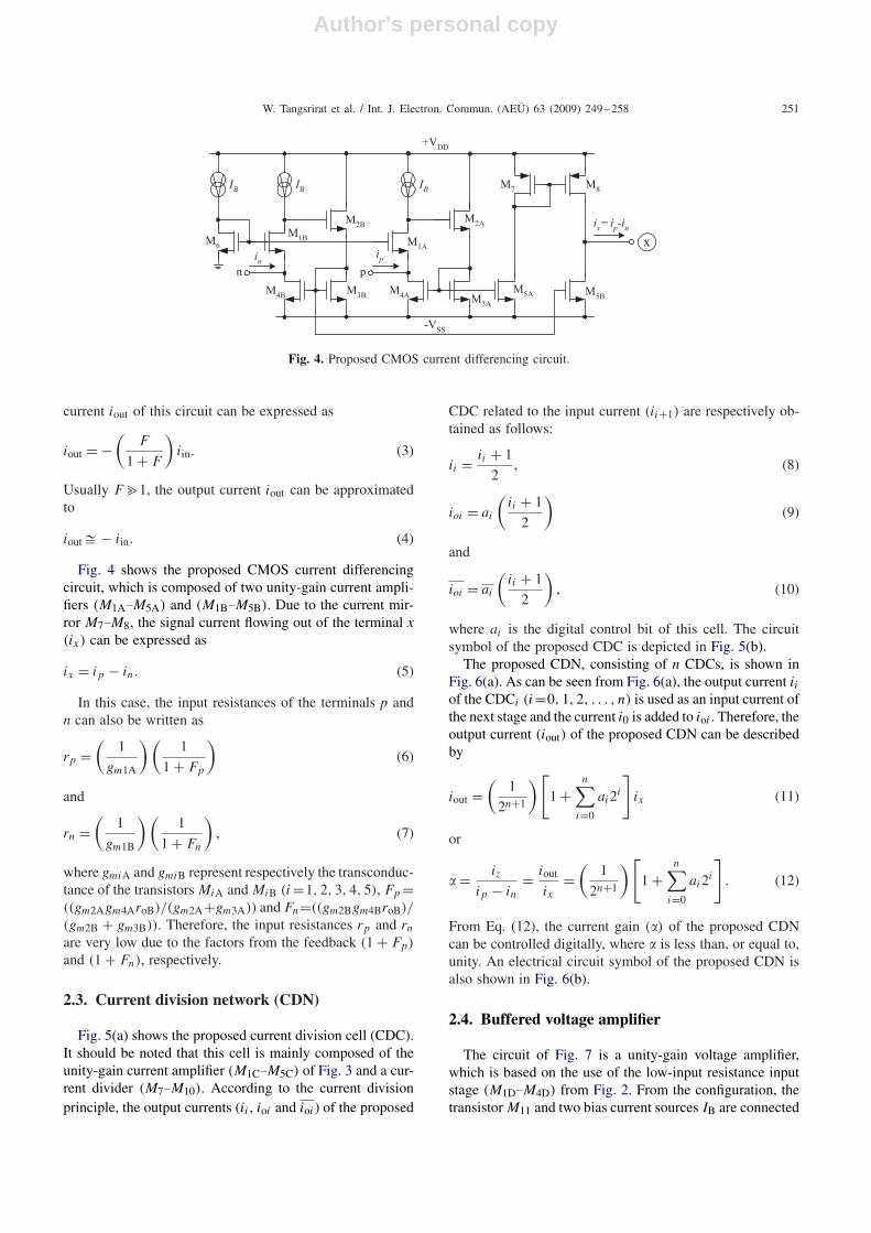
Fig. 4. Proposed CMOS current differencing circuit.
current iout of this circuit can be expressed as
iout = −(
F
1 + F
)iin. (3)
Usually F?1, the output current iout can be approximatedto
iout� − iin. (4)
Fig. 4 shows the proposed CMOS current differencingcircuit, which is composed of two unity-gain current ampli-fiers (M1A.M5A) and (M1B.M5B). Due to the current mir-ror M7.M8, the signal current flowing out of the terminal x(ix) can be expressed as
ix = ip − in. (5)
In this case, the input resistances of the terminals p andn can also be written as
rp =(
1
gm1A
) (1
1 + Fp
)(6)
and
rn =(
1
gm1B
) (1
1 + Fn
), (7)
where gmiA and gmiB represent respectively the transconduc-tance of the transistors MiA and MiB (i=1, 2, 3, 4, 5), Fp =((gm2Agm4AroB)/(gm2A+gm3A)) and Fn=((gm2Bgm4BroB)/
(gm2B + gm3B)). Therefore, the input resistances rp and rnare very low due to the factors from the feedback (1 + Fp)
and (1 + Fn), respectively.
2.3. Current division network (CDN)
Fig. 5(a) shows the proposed current division cell (CDC).It should be noted that this cell is mainly composed of theunity-gain current amplifier (M1C.M5C) of Fig. 3 and a cur-rent divider (M7.M10). According to the current divisionprinciple, the output currents (ii , ioi and ioi) of the proposed
CDC related to the input current (ii+1) are respectively ob-tained as follows:
ii = ii + 1
2, (8)
ioi = ai
(ii + 1
2
)(9)
and
ioi = ai
(ii + 1
2
), (10)
where ai is the digital control bit of this cell. The circuitsymbol of the proposed CDC is depicted in Fig. 5(b).
The proposed CDN, consisting of n CDCs, is shown inFig. 6(a). As can be seen from Fig. 6(a), the output current iiof the CDCi (i=0, 1, 2, . . . , n) is used as an input current ofthe next stage and the current i0 is added to ioi . Therefore, theoutput current (iout) of the proposed CDN can be describedby
iout =(
1
2n+1
) [1 +
n∑i=0
ai2i
]ix (11)
or
� = iz
ip − in= iout
ix=
(1
2n+1
) [1 +
n∑i=0
ai2i
]. (12)
From Eq. (12), the current gain (�) of the proposed CDNcan be controlled digitally, where � is less than, or equal to,unity. An electrical circuit symbol of the proposed CDN isalso shown in Fig. 6(b).
2.4. Buffered voltage amplifier
The circuit of Fig. 7 is a unity-gain voltage amplifier,which is based on the use of the low-input resistance inputstage (M1D.M4D) from Fig. 2. From the configuration, thetransistor M11 and two bias current sources IB are connected
Author's personal copy
252 W. Tangsrirat et al. / Int. J. Electron. Commun. (AEÜ) 63 (2009) 249–258
Fig. 5. Proposed CDC: (a) circuit diagram; (b) circuit symbol.
Fig. 6. Proposed CDN: (a) circuit diagram; (b) circuit symbol.
Fig. 7. Buffered voltage amplifier.
as voltage level shift. Therefore, the relationship of the volt-ages at the terminals w and z (or vw and vz) can be given by
vw = �vvz (13)
and
�v =(
gm11roB
1 + gm11roB
) [gm1D
(1 + gm4DroB
2
)gw + gm1D
(1 + gm4DroB
2
)]
, (14)
where gw =1/Rw and Rw is the resistor connected at the ter-minal w. If gm11roB?1 and gm1D(1 + (gm4DroB/2))?gw,then vw�vz. Since transistors M1D.M4D performs a
Author's personal copy
W. Tangsrirat et al. / Int. J. Electron. Commun. (AEÜ) 63 (2009) 249–258 253
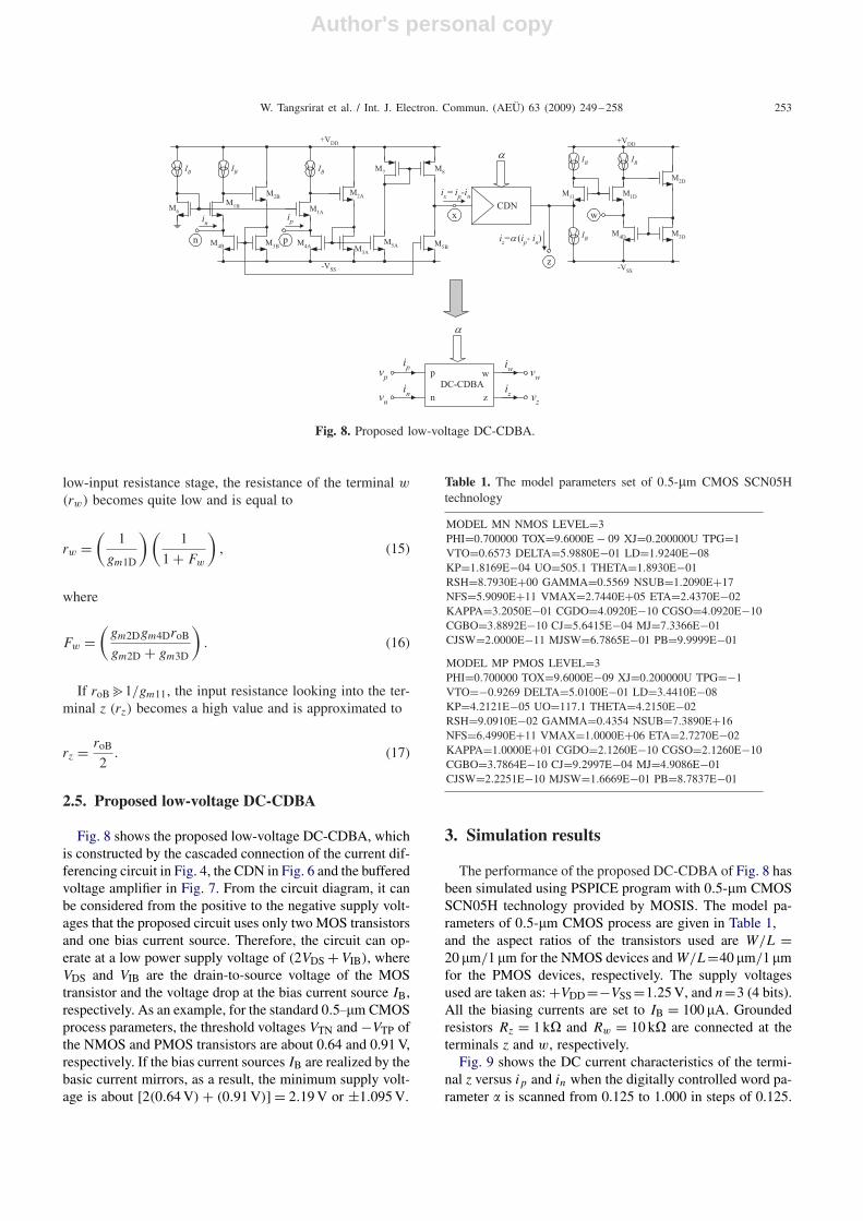
Fig. 8. Proposed low-voltage DC-CDBA.
low-input resistance stage, the resistance of the terminal w
(rw) becomes quite low and is equal to
rw =(
1
gm1D
) (1
1 + Fw
), (15)
where
Fw =(
gm2Dgm4DroB
gm2D + gm3D
). (16)
If roB?1/gm11, the input resistance looking into the ter-minal z (rz) becomes a high value and is approximated to
rz = roB
2. (17)
2.5. Proposed low-voltage DC-CDBA
Fig. 8 shows the proposed low-voltage DC-CDBA, whichis constructed by the cascaded connection of the current dif-ferencing circuit in Fig. 4, the CDN in Fig. 6 and the bufferedvoltage amplifier in Fig. 7. From the circuit diagram, it canbe considered from the positive to the negative supply volt-ages that the proposed circuit uses only two MOS transistorsand one bias current source. Therefore, the circuit can op-erate at a low power supply voltage of (2VDS +VIB), whereVDS and VIB are the drain-to-source voltage of the MOStransistor and the voltage drop at the bias current source IB,respectively. As an example, for the standard 0.5.�m CMOSprocess parameters, the threshold voltages VTN and −VTP ofthe NMOS and PMOS transistors are about 0.64 and 0.91 V,respectively. If the bias current sources IB are realized by thebasic current mirrors, as a result, the minimum supply volt-age is about [2(0.64 V) + (0.91 V)] = 2.19 V or ±1.095 V.
Table 1. The model parameters set of 0.5-�m CMOS SCN05Htechnology
MODEL MN NMOS LEVEL=3PHI=0.700000 TOX=9.6000E − 09 XJ=0.200000U TPG=1VTO=0.6573 DELTA=5.9880E−01 LD=1.9240E−08KP=1.8169E−04 UO=505.1 THETA=1.8930E−01RSH=8.7930E+00 GAMMA=0.5569 NSUB=1.2090E+17NFS=5.9090E+11 VMAX=2.7440E+05 ETA=2.4370E−02KAPPA=3.2050E−01 CGDO=4.0920E−10 CGSO=4.0920E−10CGBO=3.8892E−10 CJ=5.6415E−04 MJ=7.3366E−01CJSW=2.0000E−11 MJSW=6.7865E−01 PB=9.9999E−01
MODEL MP PMOS LEVEL=3PHI=0.700000 TOX=9.6000E−09 XJ=0.200000U TPG=−1VTO=−0.9269 DELTA=5.0100E−01 LD=3.4410E−08KP=4.2121E−05 UO=117.1 THETA=4.2150E−02RSH=9.0910E−02 GAMMA=0.4354 NSUB=7.3890E+16NFS=6.4990E+11 VMAX=1.0000E+06 ETA=2.7270E−02KAPPA=1.0000E+01 CGDO=2.1260E−10 CGSO=2.1260E−10CGBO=3.7864E−10 CJ=9.2997E−04 MJ=4.9086E−01CJSW=2.2251E−10 MJSW=1.6669E−01 PB=8.7837E−01
3. Simulation results
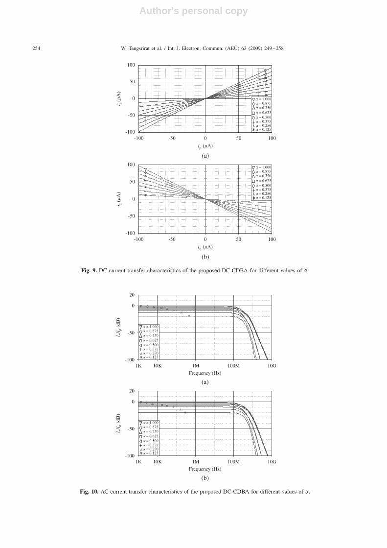
The performance of the proposed DC-CDBA of Fig. 8 hasbeen simulated using PSPICE program with 0.5-�m CMOSSCN05H technology provided by MOSIS. The model pa-rameters of 0.5-�m CMOS process are given in Table 1,and the aspect ratios of the transistors used are W/L =20 �m/1 �m for the NMOS devices and W/L=40 �m/1 �mfor the PMOS devices, respectively. The supply voltagesused are taken as: +VDD=−VSS=1.25 V, and n=3 (4 bits).All the biasing currents are set to IB = 100 �A. Groundedresistors Rz = 1 k� and Rw = 10 k� are connected at theterminals z and w, respectively.
Fig. 9 shows the DC current characteristics of the termi-nal z versus ip and in when the digitally controlled word pa-rameter � is scanned from 0.125 to 1.000 in steps of 0.125.
Author's personal copy
254 W. Tangsrirat et al. / Int. J. Electron. Commun. (AEÜ) 63 (2009) 249–258
-100 -50 0 50 100-100
-50
0
50
100
ip (�A)
i z (�A
)
-100 -50 0 50 100-100
-50
0
50
100
in (�A)
i z (�A
)
� = 1.000� = 0.875� = 0.750� = 0.625� = 0.500� = 0.375� = 0.250� = 0.125
� = 1.000� = 0.875� = 0.750� = 0.625� = 0.500� = 0.375� = 0.250� = 0.125
Fig. 9. DC current transfer characteristics of the proposed DC-CDBA for different values of �.
20
0
-50
-100
20
0
-50
-100
i z/i p
(dB
)i z
/i n (
dB)
1K 10K 1M 100M 10G
Frequency (Hz)
1K 10K 1M 100M 10G
Frequency (Hz)
� = 1.000� = 0.875� = 0.750� = 0.625� = 0.500� = 0.375� = 0.250� = 0.125
� = 1.000� = 0.875� = 0.750� = 0.625� = 0.500� = 0.375� = 0.250� = 0.125
Fig. 10. AC current transfer characteristics of the proposed DC-CDBA for different values of �.
Author's personal copy
W. Tangsrirat et al. / Int. J. Electron. Commun. (AEÜ) 63 (2009) 249–258 255
1.0
0
-1.0-1.0 -0.5 0 0.5 1.0
v w (
V)
vz (V)
vzvw
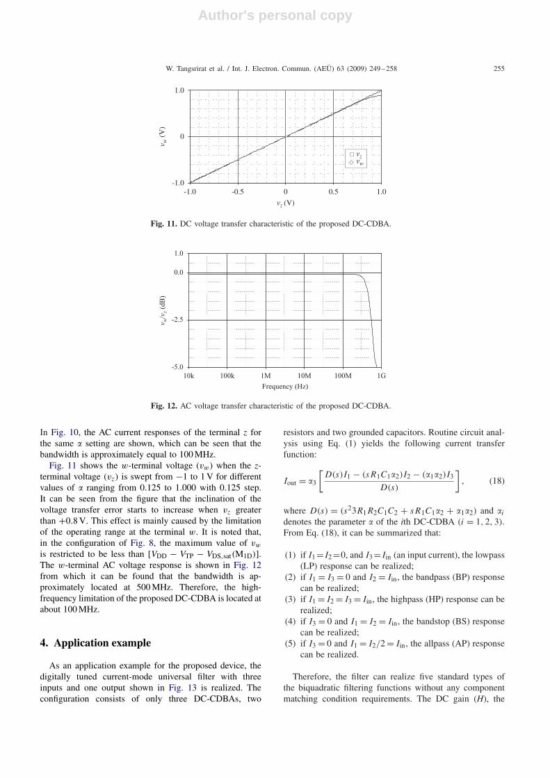
Fig. 11. DC voltage transfer characteristic of the proposed DC-CDBA.
1.0
v w/vz (
dB)
Frequency (Hz)
0.0
-2.5
-5.010k 100k 1M 10M 100M 1G
Fig. 12. AC voltage transfer characteristic of the proposed DC-CDBA.
In Fig. 10, the AC current responses of the terminal z forthe same � setting are shown, which can be seen that thebandwidth is approximately equal to 100 MHz.
Fig. 11 shows the w-terminal voltage (vw) when the z-terminal voltage (vz) is swept from −1 to 1 V for differentvalues of � ranging from 0.125 to 1.000 with 0.125 step.It can be seen from the figure that the inclination of thevoltage transfer error starts to increase when vz greaterthan +0.8 V. This effect is mainly caused by the limitationof the operating range at the terminal w. It is noted that,in the configuration of Fig. 8, the maximum value of vw
is restricted to be less than [VDD − VTP − VDS,sat(M1D)].The w-terminal AC voltage response is shown in Fig. 12from which it can be found that the bandwidth is ap-proximately located at 500 MHz. Therefore, the high-frequency limitation of the proposed DC-CDBA is located atabout 100 MHz.
4. Application example
As an application example for the proposed device, thedigitally tuned current-mode universal filter with threeinputs and one output shown in Fig. 13 is realized. Theconfiguration consists of only three DC-CDBAs, two
resistors and two grounded capacitors. Routine circuit anal-ysis using Eq. (1) yields the following current transferfunction:
Iout = �3
[D(s)I1 − (sR1C1�2)I2 − (�1�2)I3
D(s)
], (18)
where D(s) = (s23R1R2C1C2 + sR1C1�2 + �1�2) and �i
denotes the parameter � of the ith DC-CDBA (i = 1, 2, 3).From Eq. (18), it can be summarized that:
(1) if I1=I2 =0, and I3=Iin (an input current), the lowpass(LP) response can be realized;
(2) if I1 = I3 = 0 and I2 = Iin, the bandpass (BP) responsecan be realized;
(3) if I1 = I2 = I3 = Iin, the highpass (HP) response can berealized;
(4) if I3 = 0 and I1 = I2 = Iin, the bandstop (BS) responsecan be realized;
(5) if I3 = 0 and I1 = I2/2 = Iin, the allpass (AP) responsecan be realized.
Therefore, the filter can realize five standard types ofthe biquadratic filtering functions without any componentmatching condition requirements. The DC gain (H), the

Author's personal copy
256 W. Tangsrirat et al. / Int. J. Electron. Commun. (AEÜ) 63 (2009) 249–258
z
p
n
wDC-CDBA
1
R1
R2
C1
p
w
z
n
2
C2
I2
I3
p
z
w
n
3
Iout
I1DC-CDBA DC-CDBA
3
1
2
Fig. 13. Proposed digitally tuned current-mode universal filter using DC-CDBAs.
Frequency (Hz)
100
20
LPBPHPBS
0
-20
-40
-601k 10k 100k 1M 10M
Cur
rent
gai
n (d
B)
Fig. 14. Simulated frequency responses of the proposed DC-CDBA based current-mode universal filter of Fig. 13.
Frequency (Hz)
100
20
0
-20
-40
-601k 10k 100k 1M 10M
Cur
rent
gai
n (d
B)
= 1.000= 0.750= 0.500= 0.250
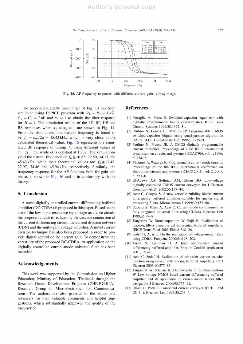
Fig. 15. BP frequency responses with different current gains �(=�1 = �2).
natural frequency (�o) and the bandwidth (�o/Q) of theproposed filter are found to be
H = �3, (19)
�o =√
�1�2
3R1R2C1C2(20)
and
�o
Q= �2
3R2C2. (21)
It can readily be shown from Eqs. (19)–(21) that the pa-rameters H, �o and �o/Q for all the filter responses can becontrolled digitally using �3, �1 and �2, respectively.
Author's personal copy
W. Tangsrirat et al. / Int. J. Electron. Commun. (AEÜ) 63 (2009) 249–258 257
100
20
Gai
n (d
B)
40
0
-20
-40-400°
-300°
-200°
-100°
0°
Phas
e (d
egre
e)
1k 10k 100k 1M 10M
Frequency (Hz)
= 1.000= 0.750= 0.500= 0.250
Gain
= 1.000= 0.750= 0.500= 0.250
Phase
Fig. 16. AP frequency responses with different current gains �(=�1 = �2).
The proposed digitally tuned filter of Fig. 13 has beensimulated using PSPICE program with R1 = R2 = 1 k�,C1 = C2 = 2 nF and �3 = 1 to obtain the filter responsefor H = 1. The simulation results of the LP, BP, HP andBS responses when �1 = �2 = 1 are shown in Fig. 14.From the simulations, the natural frequency is found tobe fo = �o/2� = 45.43 kHz, which is very close to thecalculated theoretical value. Fig. 15 represents the simu-lated BP response of tuning fo using different values of� = �1 = �2, while Q is constant at 1.732. The simulationsyield the natural frequency of fo�10.85, 22.50, 34.17 and45.43 kHz, while their theoretical values are fo�11.48,22.97, 34.46 and 45.94 kHz, respectively. Similarly, thefrequency response for the AP function, both for gain andphase, is shown in Fig. 16 and is in conformity with thetheory.
5. Conclusion
A novel digitally controlled current differencing bufferedamplifier (DC-CDBA) is proposed in this paper. Based on theuse of the low-input resistance input stage as a core circuit,the proposed circuit is realized by the cascade connection ofthe current differencing circuit, the current division network(CDN) and the unity-gain voltage amplifier. A novel currentdivision technique has also been proposed in order to pro-vide digital control on the current gain. To demonstrate theversatility of the proposed DC-CDBA, an application on thedigitally controlled current-mode universal filter has beenincluded.
Acknowledgements
This work was supported by the Commission on HigherEducation, Ministry of Education, Thailand, through theResearch Group Development Program (CHE-RG-01A),Research Group in Microelectronics for Communica-tions. The authors are also grateful to the editor andreviewers for their valuable comments and helpful sug-gestions, which substantially improved the quality of themanuscript.
References
[1] Petraglia A, Mitra S. Switched-capacitor equalizers withdigitally programmable tuning characteristics. IEEE TransCircuits Systems 1991;38:1322–31.
[2] Paulino N, Franca JE, Martins FP. Programmable CMOSswitched-capacitor biquad using quasi-passive algorithmicDAC’s. IEEE J Solid-State Circ 1995;30:715–9.
[3] Paulino N, Franca JE. A CMOS digitally programmablecurrent multiplier. Proceedings of 1996 IEEE internationalsymposium on circuits and systems (ISCAS’96), vol. 1, 1996.p. 254–7.
[4] Mazurek A, Wawryn K. Programmable current mode circuits.Proceedings of the 8th IEEE international conference onelectronics, circuits and systems (ICECS 2001), vol. 2, 2001.p. 553–6.
[5] El-Adawy AA, Soliman AM, Elwan HO. Low-voltagedigitally controlled CMOS current conveyor. Int J ElectronCommun (AEU) 2002;56:137–44.
[6] Acar C, Ozoguz S. A new versatile building block: currentdifferencing buffered amplifier suitable for analog signalprocessing filters. Microelectron J 1999;30:157–60.
[7] Ozoguz S, Toker A, Acar C. Current-mode continuous-timefully-integrated universal filter using CDBAs. Electron Lett1999;35:97–8.
[8] Tangsrirat W, Surakampontorn W, Fujii N. Realization ofleapfrog filters using current differential buffered amplifiers.IEICE Trans Fund 2003;E86-A:318–26.
[9] Sedef H, Acar C. On the realization of voltage-mode filtersusing CDBA. Frequenz 2000;54:198–202.
[10] Tarim N, Kuntman H. A high performance currentdifferencing buffered amplifier. Proc Int Conf Microelectron2001, 153–6.
[11] Acar C, Sedef H. Realization of nth-order current transferfunction using current differencing buffered amplifiers. Int JElectron 2003;90:277–83.
[12] Tangsrirat W, Klahan K, Dumawipata T, SurakampontornW. Low-voltage NMOS-based current differencing bufferedamplifier and its application to current-mode ladder filterdesign. Int J Electron 2006;93:777–91.
[13] Oliaei O, Porte J. Compound current conveyor (CCII+ andCCII−). Electron Lett 1997;33:253–4.
Author's personal copy
258 W. Tangsrirat et al. / Int. J. Electron. Commun. (AEÜ) 63 (2009) 249–258
Worapong Tangsrirat was born inUthaithani, Thailand, in 1968. He re-ceived the B.Ind.Tech. (Honors) degreein Electronics, and M.Eng. and D.Eng.degrees in Electrical Engineering allfrom Faculty of Engineering, KingMongkut’s Institute of Technology Lad-krabang (KMITL), Bangkok, Thailand,in 1991, 1997, 2003, respectively. Since1995, he has been a faculty memberat KMITL, where he is currently anAssociate Professor in the Department
of Control Engineering and serves as the leader of Mixed Sig-nal Processing Laboratory, Research Center for Communicationsand Information Technology (ReCCIT) at the same institute. Hehas several published papers in leading international journals andconferences, and has authored books on electronics and control.At present, his research interests are mainly in analog integratedcircuits and filter design.
Danucha Prasertsom received theB.Eng. (Honors) degree in Instrumen-tation System Engineering from KingMongkut’s Institute of TechnologyNorth Bangkok (KMITNB) in 2005,and M.Eng. degree in Control Engi-neering from King Mongkut’s Instituteof Technology Ladkrabang (KMITL),Bangkok, Thailand, in 2008. In 2004,he was a member of the Independentteam which won the first place of theThailand Rescue Robot Championship
2004 and was a representative team from Thailand to participatethe World Robocup Rescue Championship 2005 in Osaka, Japan.
He is currently working toward the D.Eng. degree at KMITL. Hisresearch areas are mainly in analog integrated circuits and current-mode active filter design.
Wanlop Surakampontorn receivedthe B.Eng. and M.Eng. degrees inElectrical Engineering from the KingMongkut’s Institute of TechnologyLadkrabang (KMITL), Bangkok, Thai-land, in 1976, and 1978, respectively,and the Ph.D. in Electronics from theUniversity of Kent at Canterbury, Kent,U.K., in 1983. Since 1978, he hasbeen a member of the Department ofElectronics, Faculty of Engineering,KMITL, where he is currently a Senior
Professor of Electronic Engineering. His research interests are inthe areas of analog and digital integrated circuit designs, real-timeapplication of PC computers and microprocessors, digital signalprocessing, electronic instrumentation, and VLSI signal process-ing. He is a member of the IEICE of Japan and the IEEE.